EP3087916B1 - Physiological measurement sensor - Google Patents
Physiological measurement sensorDownload PDFInfo
- Publication number
- EP3087916B1 EP3087916B1EP15165300.3AEP15165300AEP3087916B1EP 3087916 B1EP3087916 B1EP 3087916B1EP 15165300 AEP15165300 AEP 15165300AEP 3087916 B1EP3087916 B1EP 3087916B1
- Authority
- EP
- European Patent Office
- Prior art keywords
- sensor
- light
- light detector
- detector
- signal
- Prior art date
- Legal status (The legal status is an assumption and is not a legal conclusion. Google has not performed a legal analysis and makes no representation as to the accuracy of the status listed.)
- Active
Links
Images


Classifications
- A—HUMAN NECESSITIES
- A61—MEDICAL OR VETERINARY SCIENCE; HYGIENE
- A61B—DIAGNOSIS; SURGERY; IDENTIFICATION
- A61B5/00—Measuring for diagnostic purposes; Identification of persons
- A61B5/0059—Measuring for diagnostic purposes; Identification of persons using light, e.g. diagnosis by transillumination, diascopy, fluorescence
- A—HUMAN NECESSITIES
- A61—MEDICAL OR VETERINARY SCIENCE; HYGIENE
- A61B—DIAGNOSIS; SURGERY; IDENTIFICATION
- A61B5/00—Measuring for diagnostic purposes; Identification of persons
- A61B5/72—Signal processing specially adapted for physiological signals or for diagnostic purposes
- A61B5/7203—Signal processing specially adapted for physiological signals or for diagnostic purposes for noise prevention, reduction or removal
- A61B5/7207—Signal processing specially adapted for physiological signals or for diagnostic purposes for noise prevention, reduction or removal of noise induced by motion artifacts
- A61B5/7214—Signal processing specially adapted for physiological signals or for diagnostic purposes for noise prevention, reduction or removal of noise induced by motion artifacts using signal cancellation, e.g. based on input of two identical physiological sensors spaced apart, or based on two signals derived from the same sensor, for different optical wavelengths
- A—HUMAN NECESSITIES
- A61—MEDICAL OR VETERINARY SCIENCE; HYGIENE
- A61B—DIAGNOSIS; SURGERY; IDENTIFICATION
- A61B5/00—Measuring for diagnostic purposes; Identification of persons
- A61B5/02—Detecting, measuring or recording for evaluating the cardiovascular system, e.g. pulse, heart rate, blood pressure or blood flow
- A61B5/021—Measuring pressure in heart or blood vessels
- A—HUMAN NECESSITIES
- A61—MEDICAL OR VETERINARY SCIENCE; HYGIENE
- A61B—DIAGNOSIS; SURGERY; IDENTIFICATION
- A61B5/00—Measuring for diagnostic purposes; Identification of persons
- A61B5/02—Detecting, measuring or recording for evaluating the cardiovascular system, e.g. pulse, heart rate, blood pressure or blood flow
- A61B5/024—Measuring pulse rate or heart rate
- A61B5/02416—Measuring pulse rate or heart rate using photoplethysmograph signals, e.g. generated by infrared radiation
- A61B5/02427—Details of sensor
- A—HUMAN NECESSITIES
- A61—MEDICAL OR VETERINARY SCIENCE; HYGIENE
- A61B—DIAGNOSIS; SURGERY; IDENTIFICATION
- A61B5/00—Measuring for diagnostic purposes; Identification of persons
- A61B5/02—Detecting, measuring or recording for evaluating the cardiovascular system, e.g. pulse, heart rate, blood pressure or blood flow
- A61B5/024—Measuring pulse rate or heart rate
- A61B5/02438—Measuring pulse rate or heart rate with portable devices, e.g. worn by the patient
- A—HUMAN NECESSITIES
- A61—MEDICAL OR VETERINARY SCIENCE; HYGIENE
- A61B—DIAGNOSIS; SURGERY; IDENTIFICATION
- A61B5/00—Measuring for diagnostic purposes; Identification of persons
- A61B5/08—Measuring devices for evaluating the respiratory organs
- A61B5/0816—Measuring devices for examining respiratory frequency
- A—HUMAN NECESSITIES
- A61—MEDICAL OR VETERINARY SCIENCE; HYGIENE
- A61B—DIAGNOSIS; SURGERY; IDENTIFICATION
- A61B5/00—Measuring for diagnostic purposes; Identification of persons
- A61B5/68—Arrangements of detecting, measuring or recording means, e.g. sensors, in relation to patient
- A61B5/6801—Arrangements of detecting, measuring or recording means, e.g. sensors, in relation to patient specially adapted to be attached to or worn on the body surface
- A61B5/6802—Sensor mounted on worn items
- A61B5/681—Wristwatch-type devices
- A—HUMAN NECESSITIES
- A61—MEDICAL OR VETERINARY SCIENCE; HYGIENE
- A61B—DIAGNOSIS; SURGERY; IDENTIFICATION
- A61B5/00—Measuring for diagnostic purposes; Identification of persons
- A61B5/72—Signal processing specially adapted for physiological signals or for diagnostic purposes
- A61B5/7225—Details of analogue processing, e.g. isolation amplifier, gain or sensitivity adjustment, filtering, baseline or drift compensation
- A—HUMAN NECESSITIES
- A61—MEDICAL OR VETERINARY SCIENCE; HYGIENE
- A61B—DIAGNOSIS; SURGERY; IDENTIFICATION
- A61B2562/00—Details of sensors; Constructional details of sensor housings or probes; Accessories for sensors
- A61B2562/02—Details of sensors specially adapted for in-vivo measurements
- A61B2562/0233—Special features of optical sensors or probes classified in A61B5/00
- A61B2562/0238—Optical sensor arrangements for performing transmission measurements on body tissue
- A—HUMAN NECESSITIES
- A61—MEDICAL OR VETERINARY SCIENCE; HYGIENE
- A61B—DIAGNOSIS; SURGERY; IDENTIFICATION
- A61B2562/00—Details of sensors; Constructional details of sensor housings or probes; Accessories for sensors
- A61B2562/18—Shielding or protection of sensors from environmental influences, e.g. protection from mechanical damage
- A61B2562/185—Optical shielding, e.g. baffles
- A—HUMAN NECESSITIES
- A61—MEDICAL OR VETERINARY SCIENCE; HYGIENE
- A61B—DIAGNOSIS; SURGERY; IDENTIFICATION
- A61B5/00—Measuring for diagnostic purposes; Identification of persons
- A61B5/145—Measuring characteristics of blood in vivo, e.g. gas concentration or pH-value ; Measuring characteristics of body fluids or tissues, e.g. interstitial fluid or cerebral tissue
- A61B5/14532—Measuring characteristics of blood in vivo, e.g. gas concentration or pH-value ; Measuring characteristics of body fluids or tissues, e.g. interstitial fluid or cerebral tissue for measuring glucose, e.g. by tissue impedance measurement
- A—HUMAN NECESSITIES
- A61—MEDICAL OR VETERINARY SCIENCE; HYGIENE
- A61B—DIAGNOSIS; SURGERY; IDENTIFICATION
- A61B5/00—Measuring for diagnostic purposes; Identification of persons
- A61B5/145—Measuring characteristics of blood in vivo, e.g. gas concentration or pH-value ; Measuring characteristics of body fluids or tissues, e.g. interstitial fluid or cerebral tissue
- A61B5/1455—Measuring characteristics of blood in vivo, e.g. gas concentration or pH-value ; Measuring characteristics of body fluids or tissues, e.g. interstitial fluid or cerebral tissue using optical sensors, e.g. spectral photometrical oximeters
- A61B5/14551—Measuring characteristics of blood in vivo, e.g. gas concentration or pH-value ; Measuring characteristics of body fluids or tissues, e.g. interstitial fluid or cerebral tissue using optical sensors, e.g. spectral photometrical oximeters for measuring blood gases
- A61B5/14552—Details of sensors specially adapted therefor
- A—HUMAN NECESSITIES
- A61—MEDICAL OR VETERINARY SCIENCE; HYGIENE
- A61B—DIAGNOSIS; SURGERY; IDENTIFICATION
- A61B5/00—Measuring for diagnostic purposes; Identification of persons
- A61B5/145—Measuring characteristics of blood in vivo, e.g. gas concentration or pH-value ; Measuring characteristics of body fluids or tissues, e.g. interstitial fluid or cerebral tissue
- A61B5/1455—Measuring characteristics of blood in vivo, e.g. gas concentration or pH-value ; Measuring characteristics of body fluids or tissues, e.g. interstitial fluid or cerebral tissue using optical sensors, e.g. spectral photometrical oximeters
- A61B5/14558—Measuring characteristics of blood in vivo, e.g. gas concentration or pH-value ; Measuring characteristics of body fluids or tissues, e.g. interstitial fluid or cerebral tissue using optical sensors, e.g. spectral photometrical oximeters by polarisation
Definitions
- the present applicationgenerally relates to physiological measurement sensors.
- Various metering devices that measure physiological conditions of userssuch as pulse sensors have become common for people to measure their own heart rate, movements or other parameters.
- the measurementscan be performed using a chest strap that is worn under clothes or using a wrist worn watch-like sensor device.
- Pulse or heart ratecan be monitored for example optically using a photoplethymography (PPG) sensor.
- PPGphotoplethymography
- Optical heart rate measurementrequires that the sensor is kept very stably on the wrist during the measurement as the photoplethysmographic (PPG) measurement is sensitive to all kind of movements of the sensor. Motion artifacts caused by sensor movements corrupt the pulsatile heart rate (HR) signal and confuse the HR monitoring algorithms of the sensor. The end result is that the calculated HR in beats per minute (bpm) is wrong.
- the wrist strapcannot be kept too tight, because it would be inconvenient / unpleasant for the user and might even stop or deteriorate blood circulation in small vessels thereby causing the measurement signal to disappear.
- a sensor according to claim 1According to a first aspect of the present invention, there is provided a sensor according to claim 1.
- the senorfurther comprises a light source configured to emit light at the target wavelength.
- the subtraction elementis an analog subtraction circuit. In an example embodiment, the subtraction element is digital.
- the senorcomprises a signal processing element configured to process the subtracted signal to produce the physiological measurement result.
- the first light detector and the second light detectorcomprise similar or identical characteristics. In an example embodiment, all characteristic of the light detectors are not necessarily similar.
- the first light detector and the second light detectorare integrated components on a common substrate.
- the first light detector and the second light detectorare connected in parallel with opposite polarities.
- the senorcomprises light-scattering material arranged so that the light that enters the sensor passes through the light-scattering material prior to entering the first light detector and the second light detector.
- the first light detector and the second light detectorform a detector pair and the sensor comprises a plurality of said detector pairs forming a detector array.
- the optical blocking filteris a notch filter or a band-stop filter.
- the optical blocking filteris further enhanced with an additional band-pass filter.
- the methodfurther comprises connecting the first light detector and the second light detector in parallel with opposite polarities.
- a new type of sensor for optical measurement of physiological conditions of a usermeasures physiological conditions of a user and produces sensor signals corresponding to a property of the matter underlying the skin of the user (capillaries and veins, for example).
- the sensoris particularly suited for user wearable devices.
- various example embodimentsare discussed in connection with optical heart rate sensors.
- Physiological conditions or physiological measurement results referred to hereinmay include one or more of the following: heart rate, respiration rate, blood pressure, oxygen saturation level, and glucose level. Also other physiological condition measurements may apply.
- FIG. 1is a simplified illustration of an example optical heart rate measurement.
- Fig. 1shows a (reflective type) PPG sensor that comprises a LED (light emitting diode) 101, a light source, and a photo transistor 102, a light detector. Also a photo diode (PD) may be used as the light detector.
- the LED (optical emitter, light source) 101emits light and the light detector 102 receives light rays reflected from a wrist 103 of a user.
- the sensorproduces sensor signals based on the light detected by the light detector 102.
- an optical sensorwith two light detectors (e.g. photo diodes).
- one of the light detectorsis sensitive to a range of wavelengths and the other one of the light detectors is insensitive to a certain target wavelength.
- the target wavelengthis the wavelength one is interested in and the target wavelength may comprise a certain wavelength band.
- the filteris a blocking filter.
- the filtermay be for example a notch filter or a band-stop filter, such as a dichroic mirror/reflector.
- the filteris configured to block a target wavelength, which is the wavelength one is interested in.
- the sensorcomprises a light source that emits light at a certain wavelength. This wavelength is the target wavelength and the blocking filter matches the wavelength of the light source. That is, the blocking filter is configured to filter out or block the wavelength of the light source.
- the light sourceis a green LED working at 525 nm peak wavelength and the blocking filter filters out the 525 nm wavelength. This is however only one example and other wavelengths can be equally used.
- the other one of the light detectorsis used as is without additional optical band-stop filtering. That is, the other light detector detects a range of wavelengths.
- the detectorsdetect light
- the detectorthat is insensitive to the target wavelengths and e.g. covered with the filter, detects less the target light than the other one.
- the detected light signalsare subtracted from each other to produce a result signal that is cleared from noise and artifacts originating from unwanted wavelengths.
- there is an analog circuitconfigured to perform the subtraction.
- the detected signalsare analog-to-digital converted and then subtracted digitally. The resulting signal may then be used for producing a physiological measurement result, such as heart rate.
- Fig. 2is a simplified illustration of an example physiological condition sensor.
- the physiological condition sensor 203is attached to a wrist strap 202 that allows the sensor 203 to be fitted around a wrist of the user.
- the sensor 203can be made of a suitable material, such as for example plastic (e.g. acrylonitrile butadiene styrene (ABS) or polycarbonate (PC)), carbon fiber materials, glass, wood, metal, ceramics or other material covered with fabric or leather or any combination of these.
- the strapmay be made of suitable flexible or bendable material, such as plastic, fabric, and leather.
- the strap 202 and the sensor 203are integrally formed of one piece of material.
- the materialcan comprise or consist of any of the following: plastics, metals, nano-fibers, carbon fiber, leather, fabric and glass.
- Fig 2shows the sensor attached to a wrist strap, but the sensor may equally be part of some other user wearable apparatus that can be fitted around a body part (e.g. wrist, ankle or finger) of a user.
- the sensormay be configured to be integrated into a garment of a user.
- the sensormay be attached or integrated for example to a belt, a sock, a shoe, a sleeve or a collar of a shirt or pullover, and/or a waistband of trousers or skirt.
- the sensormay be detachable from the garment.
- the sensormay be shaped like a watch and it may be configured to display time or other useful information to the user.
- the sensormay be attached to a patch/plaster (with adhesive) or to a ring.
- a further alternativeis that the sensor is attached to an ear of the user.
- the sensormay be part of an earplug, for example.
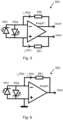
- Fig. 3Ais a schematic drawing illustrating an example. The aim is to detect signals at a certain target wavelength in a sensor.
- Figure 3shows a light source 301 (e.g. a LED) and a first light detector 302 (e.g. a photo diode) and a second light detector 303 (e.g. a photo diode).
- the second light detector 303is covered with a filter 304 that is configured to block or eliminate the target wavelength.
- the filter 304is for example a notch filter or a band-stop filter.
- the filter 304is a dichroic mirror/reflector. Dichroic mirror/reflector can be very steep and therefore they may suit well embodiments of the invention.
- the example of Fig 3Aoperates as follows:
- the light source 301emits light.
- the lightreflects from skin/tissue of a user and the reflected light arrives at the light detectors 302 and 303.
- the first light detector 302detects all wavelengths of the reflected light.
- the second light detector 303detects all other wavelengths of the reflected light except the wavelength(s) blocked by the filter 304.
- the first light detector 302produces a first detected signal and the second light detector 303 produces a second detected signal.
- the second detected signalis then subtracted from the first detected signal.
- the subtractioncan be done either in an analog circuit or digitally e.g. afterwards as a part of the digital signal processing.
- the subtractionmay be performed at the very beginning of a chain of analog signal condition stage of sensor electronics e.g. before any amplification is applied. Whichever approach is chosen, the use of subtracted signal reduces the complexity of the needed digital correction, e.g. motion artifact compensation. In an embodiment the digital signal correction may not be necessarily needed at all.
- the light detectors 302 and 303are further covered with a band-pass filter that lets through mainly only the peak/target wavelength. In this way the detection results may be further improved as the band-pass filtering reduces the amount of unwanted wavelengths.
- the light sourceemits light at a certain wavelength, e.g. green light with 525 nm peak wavelength, and the target is to detect this wavelength.
- the filter 304is configured to block this certain wavelength, e.g. the wavelength 525 nm.
- Other wavelengthsare possible, too, and even white light (broadband light source) or ambient light may be used.
- Fig. 3Bdepicts example bandwidths of an example filter and light source.
- Dotted line 350depicts bandwidth of a light source and solid line 360 depicts bandwidth of the filter.
- the bandwidths of the light source and the filterhappen to be similar.
- the bandwidth of the filtermay be narrower and/or the bandwidth of the light source may be wider.
- a target wavelength 370i.e. the wavelength of interest, comprises the center wavelength of the bandwidths.
- the target wavelengthmay comprise certain range near the center wavelength.
- the filter depicted in Fig. 3Bis a band-stop filter.
- a notch filterwould be sharper and the bandwidth of a notch filter would be narrower than the depicted bandwidth.
- the senordoes not include the light source 301. Instead ambient light is used for sensing the physiological conditions in the sensor. For example ambient light reflected from the skin/tissue of the user is detected by the light detectors 302 and 303.
- FIG. 3Cis a schematic drawing illustrating another example embodiment comprising a plurality of detector pairs.
- Figure 3Cshows a light source 301, a first light detector 302, a second light detector 303, a third light detector 312, and a fourth light detector 313.
- the light sourceis for example a LED and the light detectors are for example photo diodes.
- the second light detector 303is covered with a filter 304 that is configured to block or eliminate a certain wavelength.
- the first light detector 302 and the second light detector 303from a first detector pair 310.
- the fourth light detector 313is covered with a filter 314 that is configured to block or eliminate a certain wavelength.
- the third light detector 312 and the fourth light detector 313from a second detector pair 320.
- Detection of signals by each detector pair in Fig. 3Cis performed in a similar manner as disclosed in the foregoing in connection with Fig. 3A .
- the aimis to detect signals at a certain target wavelength and the filters 304 and 314 are configured to block this target wavelength.
- Resulting signals obtained from different detector pairs 310, 320may be combined in a suitable manner. For example, average of the resulting signals from different detector pairs can be used.
- different detector pairs 310, 320are configured to detect different wavelengths, that is, there may be more than one target wavelength to be detected. In this case there is at least one detector pair for each target wavelength and the filter comprised in different detector pairs matches the target wavelength of that particular detector pair.
- the sensormay comprise multiple light sources, each of which emits different wavelength or there may be only one light source.
- different wavelengthsare typically detected sequentially. That is, it has been feasible to detect only one wavelength at a time. With the solution of various embodiments of the invention, it is possible to detect different wavelengths at the same time as the disclosed structure efficiently removes unwanted wavelengths from the final detected signal. Therefore the detector pairs 310, 320 are sufficiently wavelength selective to allow simultaneous detection of different wavelengths.
- Fig. 3Cshows two detector pairs, but there may be even more detector pairs.
- the detector pairsmay form an array of detectors.
- the light detectors in Figs. 3A and 3Cmay be covered with a light-scattering material to evenly spread out the incoming light to all light detectors.
- the light-scattering materialmay be a light-scattering material film or lens or optical diffuser.
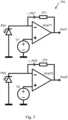
- Figs. 4A and 4Bare logical block diagrams of sensors. A chain of logical processing blocks is illustrated. It is to be noted that the shown logical blocks do not necessarily correspond to separate physical blocks. Instead functionality of a plurality of logical blocks may be implemented in one physical electronic circuit, for example. Furthermore, the order of the logical blocks may vary from the shown examples.
- Fig. 4Aillustrates an analog subtraction example
- Fig. 4Billustrates a digital subtraction example.
- the sensor of Fig. 4Acomprises a light detector block 401, a subtraction element 402, an analog front-end (AFE) block 403, an analog-to-digital conversion (ADC) block 404 and a signal processing block 405 connected into a chain.
- the light detector block 401comprises two light detectors (or even more than two light detectors as disclosed in connection with Fig. 3C ).
- the subtraction element 402is an analog circuit that combines the signals detected by the light detectors and produces a subtracted signal.
- the analog front-end block 403performs signal processing in analog domain. For example amplification, filtering and/or conditioning may be performed.
- the signalis analog-to-digital converted in block 404.
- the signal processing block 405produces final physiological measurement results (e.g. heart rate) based on the sensor signal obtained from blocks 401-404.
- the signal processing block 405may apply further correction algorithms to the sensor signal if necessary.
- the sensor of Fig. 4Bcomprises a light detector block 401, an analog front-end (AFE) block 413, an analog-to-digital conversion block 414, a subtraction element 412 and a signal processing block 405 connected into a chain.
- the light detector block 401comprises two light detectors (or even more than two light detectors as disclosed in connection with Fig. 3C ).
- the signals detected by the two light detectors in the light detector block 401are separately processed in the analog front-end block 414 (e.g. amplified, filtered and/or conditioned) and analog-to-digital converted in block414 and the two signals are combined in the digital subtraction element 412.
- the subtraction element 412is digital in this example.
- the subtraction elementmay be part of the signal processing block 405.
- the signal processing block 405produces final physiological measurement results (e.g. heart rate) based on the sensor signal obtained from blocks 401, 413, 414 and 412.
- the signal processing block 405may apply further correction algorithms
- Figs. 5-8are circuit diagrams of example embodiments. In the shown examples there are two photo diodes PD1 and PD2 operating as the light detectors.
- the photo diodes PD1 and PD2are arranged in parallel connection with opposite polarities. That is, the photo diodes are connected back-to-back in parallel. It is feasible to use such back-to-back arrangement in the shown example circuits as the feedback mechanism of the amplifier maintains zero bias (DC) across both photo diodes PD1 and PD2. In this way PD1 does not get reverse biased and PD2 does not get forward biased, or vice versa.
- DCzero bias
- Fig. 5shows a fully differential detection circuit 500.
- the circuitcomprises the photo diodes PD1 and PD2, two impedances Z51 and Z52 and an amplifier Amp51.
- the circuit 500provides voltages Vout- and Vout+ representative of the difference between light detected by the photo diodes PD1 and PD2.
- the circuit of Fig. 5implements the blocks 401, 402 and part of the 403 of Fig. 4A .
- Fig. 6shows a single-ended detection circuit 600.
- the circuitcomprises the photo diodes PD1 and PD2, an impedance Z61 and an amplifier Amp61.
- the circuit 600provides voltage Vout representative of difference between the light detected by the photo diodes PD1 and PD2.
- the circuit of Fig. 6implements the blocks 401, 402 and part of the 403 of Fig. 4A .
- Fig. 7shows a single-ended detection circuit 700 with optional biasing and separated outputs. Photoconductive mode is shown in Fig. 7 .
- the circuitcomprises the photo diodes PD1 and PD2, voltage sources V1 and V2, impedances Z71 and Z72, and amplifiers Amp71 and Amp72.
- As an output the circuit 700provides voltages Vout1 and Vout2 representative of the light detected by the photo diodes PD1 and PD2 respectively.
- the circuit of Fig. 7implements the block 401 of Fig. 4A .
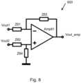
- Fig. 8shows a difference amplifier 800.
- the circuitcomprises impedances Z81-Z84 and an amplifier Amp81.
- the outputs Vout1 and Vout2 of the circuit of Fig. 7may be connected to inputs of the difference amplifier 800.
- the difference amplifier 800produces an output voltage Vout_amp that is representative of the difference between the voltages Vout1 and Vout2.
- the circuit of Fig. 8implements the blocks 402 and part of the 403 of Fig. 4A . That is, the circuits of Figs. 7 and 8 implement the blocks 401-403 of Fig. 4A .
- Figs. 5-8do not show the optical blocking filter in front of or on top of one of the photo diodes PD1 and PD2. Clearly such filter is included in practical implementations.
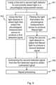
- Fig. 9shows a flow chart of a process.
- the processcomprises:
- a technical effect of one or more of the example embodiments disclosed hereinis that an improved optical sensor is provided.
- analog solution provided in various example embodimentsmay be faster and more robust than digital solutions.
- Another technical effect of one or more of the example embodiments disclosed hereinis that a need to develop and use complex software algorithms to correct the measurement signal may be reduced. Instead simpler algorithms may be applied.
- DC component of a measured signalis reduced.
- DCis not an interesting component and the presence of the DC component only narrows down the effective dynamic range of an analog front-end.
- Another technical effect of one or more of the example embodiments disclosed hereinis that the solution is easy to take into use.
- Various example solutionsare compatible with existing optical measurement ICs (integrated circuits) and/or can be easily made compatible with existing optical measurement ICs.
- Another technical effect of one or more of the example embodiments disclosed hereinis that concurrent measurement using two or more wavelengths is enabled.
- the photo diode configuration of various embodimentsmakes the photo diode extremely wavelength selective and therefore it is possible to measure two or more wavelengths at the same time.
- time multiplexingis often utilized for multi-wavelength measurements, that is, different wavelengths are measured at different time periods.
- Another technical effect of one or more of the example embodiments disclosed hereinis that the solution is less sensitive to ambient and other unwanted light sources.
- Another technical effect of one or more of the example embodiments disclosed hereinis that a wide spectrum light source can be used. For example wider spectrum than spectrum provided by LEDs could be used.
- the different functions discussed hereinmay be performed in a different order and/or concurrently with each other. Furthermore, if desired, one or more of the before-described functions may be optional or may be combined.
Landscapes
- Health & Medical Sciences (AREA)
- Life Sciences & Earth Sciences (AREA)
- Engineering & Computer Science (AREA)
- General Health & Medical Sciences (AREA)
- Public Health (AREA)
- Veterinary Medicine (AREA)
- Animal Behavior & Ethology (AREA)
- Surgery (AREA)
- Physics & Mathematics (AREA)
- Molecular Biology (AREA)
- Biophysics (AREA)
- Pathology (AREA)
- Biomedical Technology (AREA)
- Heart & Thoracic Surgery (AREA)
- Medical Informatics (AREA)
- Physiology (AREA)
- Cardiology (AREA)
- Signal Processing (AREA)
- Pulmonology (AREA)
- Psychiatry (AREA)
- Artificial Intelligence (AREA)
- Computer Vision & Pattern Recognition (AREA)
- Vascular Medicine (AREA)
- Power Engineering (AREA)
- Measurement Of The Respiration, Hearing Ability, Form, And Blood Characteristics Of Living Organisms (AREA)
- Measuring Pulse, Heart Rate, Blood Pressure Or Blood Flow (AREA)
Description
- The present application generally relates to physiological measurement sensors.
- This section illustrates useful background information without admission of any technique described herein representative of the state of the art.
- Various metering devices that measure physiological conditions of users such as pulse sensors have become common for people to measure their own heart rate, movements or other parameters. The measurements can be performed using a chest strap that is worn under clothes or using a wrist worn watch-like sensor device.
- Pulse or heart rate can be monitored for example optically using a photoplethymography (PPG) sensor. Optical heart rate measurement requires that the sensor is kept very stably on the wrist during the measurement as the photoplethysmographic (PPG) measurement is sensitive to all kind of movements of the sensor. Motion artifacts caused by sensor movements corrupt the pulsatile heart rate (HR) signal and confuse the HR monitoring algorithms of the sensor. The end result is that the calculated HR in beats per minute (bpm) is wrong.
- However, keeping the sensor completely stably on the wrist is difficult in practice. For example, the wrist strap cannot be kept too tight, because it would be inconvenient / unpleasant for the user and might even stop or deteriorate blood circulation in small vessels thereby causing the measurement signal to disappear.
- An optical heart rate sensor according to the state of the art is for instance described in
US2012/0197137A1 . - The invention is defined in the claims.
- According to a first aspect of the present invention, there is provided a sensor according to claim 1.
- In an example embodiment, the sensor further comprises a light source configured to emit light at the target wavelength.
- In an example embodiment, the subtraction element is an analog subtraction circuit. In an example embodiment, the subtraction element is digital.
- In an example embodiment, the sensor comprises a signal processing element configured to process the subtracted signal to produce the physiological measurement result. In an example embodiment, the first light detector and the second light detector comprise similar or identical characteristics. In an example embodiment, all characteristic of the light detectors are not necessarily similar.
- In an example embodiment, the first light detector and the second light detector are integrated components on a common substrate.
- In an example embodiment, the first light detector and the second light detector are connected in parallel with opposite polarities.
- In an example embodiment, the sensor comprises light-scattering material arranged so that the light that enters the sensor passes through the light-scattering material prior to entering the first light detector and the second light detector.
- In an example embodiment, the first light detector and the second light detector form a detector pair and the sensor comprises a plurality of said detector pairs forming a detector array.
- In an example embodiment, the optical blocking filter is a notch filter or a band-stop filter.
- In an example embodiment, the optical blocking filter is further enhanced with an additional band-pass filter.
- According to a second aspect of the present invention, there is provided a user wearable apparatus according to claim 12.
- According to a third aspect of the present invention, there is provided a method according to claim 13.
- In an example embodiment, the method further comprises connecting the first light detector and the second light detector in parallel with opposite polarities.
- Different non-binding example aspects have been illustrated in the foregoing. The embodiments in the foregoing are used merely to explain selected aspects or steps that may be utilized. Some embodiments may be presented only with reference to certain example aspects . It should be appreciated that corresponding embodiments may apply to other example aspects as well.
- For a more complete understanding of example embodiments of the present invention, reference is now made to the following descriptions taken in connection with the accompanying drawings in which:
Fig. 1 is a simplified illustration of an example optical heart rate measurement;Fig. 2 is a simplified illustration of an example physiological measurement sensor;Fig. 3A is a schematic drawing illustrating an example embodiment;Fig. 3B depicts example bandwidths of an example filter and light source;Fig. 3C is a schematic drawing illustrating another example embodiment;Figs. 4A and 4B are logical block diagrams of sensors of example embodiments;Figs. 5-8 are circuit diagrams of example embodiments; andFig. 9 shows a flow chart of a process of an example embodiment.- Example embodiments of the present invention and its potential advantages are understood by referring to
Figs. 1 through 12 of the drawings. In this document, like reference signs denote like parts or steps. - In various example embodiments of the invention there is provided a new type of sensor for optical measurement of physiological conditions of a user. The sensor measures physiological conditions of a user and produces sensor signals corresponding to a property of the matter underlying the skin of the user (capillaries and veins, for example). The sensor is particularly suited for user wearable devices. In the following, various example embodiments are discussed in connection with optical heart rate sensors. Physiological conditions or physiological measurement results referred to herein may include one or more of the following: heart rate, respiration rate, blood pressure, oxygen saturation level, and glucose level. Also other physiological condition measurements may apply.
- Heart rate can be monitored optically by measuring variations in blood volume with a photoplethymography (PPG) sensor.
Fig. 1 is a simplified illustration of an example optical heart rate measurement.Fig. 1 shows a (reflective type) PPG sensor that comprises a LED (light emitting diode) 101, a light source, and aphoto transistor 102, a light detector. Also a photo diode (PD) may be used as the light detector. The LED (optical emitter, light source) 101 emits light and thelight detector 102 receives light rays reflected from awrist 103 of a user. The sensor produces sensor signals based on the light detected by thelight detector 102. - There is provided an optical sensor with two light detectors (e.g. photo diodes). In an embodiment one of the light detectors is sensitive to a range of wavelengths and the other one of the light detectors is insensitive to a certain target wavelength. The target wavelength is the wavelength one is interested in and the target wavelength may comprise a certain wavelength band.
- One of the light detectors is covered with an optical filter that is configured to block some wavelengths or prevent some wavelengths from passing through the filter. The filter is a blocking filter. The filter may be for example a notch filter or a band-stop filter, such as a dichroic mirror/reflector. The filter is configured to block a target wavelength, which is the wavelength one is interested in. In an embodiment, the sensor comprises a light source that emits light at a certain wavelength. This wavelength is the target wavelength and the blocking filter matches the wavelength of the light source. That is, the blocking filter is configured to filter out or block the wavelength of the light source. In an example embodiment the light source is a green LED working at 525 nm peak wavelength and the blocking filter filters out the 525 nm wavelength. This is however only one example and other wavelengths can be equally used. The other one of the light detectors is used as is without additional optical band-stop filtering. That is, the other light detector detects a range of wavelengths.
- Now, when the light detectors detect light, the detector that is insensitive to the target wavelengths and e.g. covered with the filter, detects less the target light than the other one. The detected light signals are subtracted from each other to produce a result signal that is cleared from noise and artifacts originating from unwanted wavelengths. In an embodiment there is an analog circuit configured to perform the subtraction. In another alternative the detected signals are analog-to-digital converted and then subtracted digitally. The resulting signal may then be used for producing a physiological measurement result, such as heart rate.
Fig. 2 is a simplified illustration of an example physiological condition sensor. Thephysiological condition sensor 203 is attached to awrist strap 202 that allows thesensor 203 to be fitted around a wrist of the user.- The
sensor 203 can be made of a suitable material, such as for example plastic (e.g. acrylonitrile butadiene styrene (ABS) or polycarbonate (PC)), carbon fiber materials, glass, wood, metal, ceramics or other material covered with fabric or leather or any combination of these. The strap may be made of suitable flexible or bendable material, such as plastic, fabric, and leather. In an example embodiment, thestrap 202 and thesensor 203 are integrally formed of one piece of material. The material can comprise or consist of any of the following: plastics, metals, nano-fibers, carbon fiber, leather, fabric and glass. Fig 2 shows the sensor attached to a wrist strap, but the sensor may equally be part of some other user wearable apparatus that can be fitted around a body part (e.g. wrist, ankle or finger) of a user. The sensor may be configured to be integrated into a garment of a user. The sensor may be attached or integrated for example to a belt, a sock, a shoe, a sleeve or a collar of a shirt or pullover, and/or a waistband of trousers or skirt. The sensor may be detachable from the garment. The sensor may be shaped like a watch and it may be configured to display time or other useful information to the user. The sensor may be attached to a patch/plaster (with adhesive) or to a ring. A further alternative is that the sensor is attached to an ear of the user. The sensor may be part of an earplug, for example.Fig. 3A is a schematic drawing illustrating an example. The aim is to detect signals at a certain target wavelength in a sensor.Figure 3 shows a light source 301 (e.g. a LED) and a first light detector 302 (e.g. a photo diode) and a second light detector 303 (e.g. a photo diode). The secondlight detector 303 is covered with afilter 304 that is configured to block or eliminate the target wavelength.- The
filter 304 is for example a notch filter or a band-stop filter. In an embodiment thefilter 304 is a dichroic mirror/reflector. Dichroic mirror/reflector can be very steep and therefore they may suit well embodiments of the invention. - The example of
Fig 3A operates as follows: Thelight source 301 emits light. The light reflects from skin/tissue of a user and the reflected light arrives at thelight detectors first light detector 302 detects all wavelengths of the reflected light. The secondlight detector 303 detects all other wavelengths of the reflected light except the wavelength(s) blocked by thefilter 304. Thefirst light detector 302 produces a first detected signal and the secondlight detector 303 produces a second detected signal. The second detected signal is then subtracted from the first detected signal. The subtraction can be done either in an analog circuit or digitally e.g. afterwards as a part of the digital signal processing. If analog subtraction is used, the subtraction may be performed at the very beginning of a chain of analog signal condition stage of sensor electronics e.g. before any amplification is applied. Whichever approach is chosen, the use of subtracted signal reduces the complexity of the needed digital correction, e.g. motion artifact compensation. In an embodiment the digital signal correction may not be necessarily needed at all. - In an embodiment the
light detectors - In an embodiment the light source emits light at a certain wavelength, e.g. green light with 525 nm peak wavelength, and the target is to detect this wavelength. In that case, the
filter 304 is configured to block this certain wavelength, e.g. the wavelength 525 nm. Other wavelengths are possible, too, and even white light (broadband light source) or ambient light may be used. Fig. 3B depicts example bandwidths of an example filter and light source.Dotted line 350 depicts bandwidth of a light source andsolid line 360 depicts bandwidth of the filter. In the shown example the bandwidths of the light source and the filter happen to be similar. In alternative examples the bandwidth of the filter may be narrower and/or the bandwidth of the light source may be wider. Atarget wavelength 370, i.e. the wavelength of interest, comprises the center wavelength of the bandwidths. The target wavelength may comprise certain range near the center wavelength. The filter depicted inFig. 3B is a band-stop filter. A notch filter would be sharper and the bandwidth of a notch filter would be narrower than the depicted bandwidth.- In an example embodiment the sensor does not include the
light source 301. Instead ambient light is used for sensing the physiological conditions in the sensor. For example ambient light reflected from the skin/tissue of the user is detected by thelight detectors Fig. 3C is a schematic drawing illustrating another example embodiment comprising a plurality of detector pairs.Figure 3C shows alight source 301, afirst light detector 302, a secondlight detector 303, a thirdlight detector 312, and a fourthlight detector 313. The light source is for example a LED and the light detectors are for example photo diodes. The secondlight detector 303 is covered with afilter 304 that is configured to block or eliminate a certain wavelength. Thefirst light detector 302 and the secondlight detector 303 from afirst detector pair 310. The fourthlight detector 313 is covered with afilter 314 that is configured to block or eliminate a certain wavelength. The thirdlight detector 312 and the fourthlight detector 313 from asecond detector pair 320.- Detection of signals by each detector pair in
Fig. 3C is performed in a similar manner as disclosed in the foregoing in connection withFig. 3A . - The aim is to detect signals at a certain target wavelength and the
filters - In an embodiment different detector pairs 310, 320 are configured to detect different wavelengths, that is, there may be more than one target wavelength to be detected. In this case there is at least one detector pair for each target wavelength and the filter comprised in different detector pairs matches the target wavelength of that particular detector pair. In this case the sensor may comprise multiple light sources, each of which emits different wavelength or there may be only one light source. In prior art solutions, different wavelengths are typically detected sequentially. That is, it has been feasible to detect only one wavelength at a time. With the solution of various embodiments of the invention, it is possible to detect different wavelengths at the same time as the disclosed structure efficiently removes unwanted wavelengths from the final detected signal. Therefore the detector pairs 310, 320 are sufficiently wavelength selective to allow simultaneous detection of different wavelengths.
Fig. 3C shows two detector pairs, but there may be even more detector pairs. The detector pairs may form an array of detectors.- In an embodiment the light detectors in
Figs. 3A and3C may be covered with a light-scattering material to evenly spread out the incoming light to all light detectors. The light-scattering material may be a light-scattering material film or lens or optical diffuser. Figs. 4A and 4B are logical block diagrams of sensors. A chain of logical processing blocks is illustrated. It is to be noted that the shown logical blocks do not necessarily correspond to separate physical blocks. Instead functionality of a plurality of logical blocks may be implemented in one physical electronic circuit, for example. Furthermore, the order of the logical blocks may vary from the shown examples.Fig. 4A illustrates an analog subtraction example andFig. 4B illustrates a digital subtraction example.- The sensor of
Fig. 4A comprises alight detector block 401, asubtraction element 402, an analog front-end (AFE) block 403, an analog-to-digital conversion (ADC) block 404 and asignal processing block 405 connected into a chain. Thelight detector block 401 comprises two light detectors (or even more than two light detectors as disclosed in connection withFig. 3C ). Thesubtraction element 402 is an analog circuit that combines the signals detected by the light detectors and produces a subtracted signal. The analog front-end block 403 performs signal processing in analog domain. For example amplification, filtering and/or conditioning may be performed. The signal is analog-to-digital converted inblock 404. Thesignal processing block 405 produces final physiological measurement results (e.g. heart rate) based on the sensor signal obtained from blocks 401-404. Thesignal processing block 405 may apply further correction algorithms to the sensor signal if necessary. - The sensor of
Fig. 4B comprises alight detector block 401, an analog front-end (AFE) block 413, an analog-to-digital conversion block 414, asubtraction element 412 and asignal processing block 405 connected into a chain. Thelight detector block 401 comprises two light detectors (or even more than two light detectors as disclosed in connection withFig. 3C ). The signals detected by the two light detectors in thelight detector block 401 are separately processed in the analog front-end block 414 (e.g. amplified, filtered and/or conditioned) and analog-to-digital converted in block414 and the two signals are combined in thedigital subtraction element 412. Thesubtraction element 412 is digital in this example. The subtraction element may be part of thesignal processing block 405. Thesignal processing block 405 produces final physiological measurement results (e.g. heart rate) based on the sensor signal obtained fromblocks signal processing block 405 may apply further correction algorithms to the sensor signal if necessary. Figs. 5-8 are circuit diagrams of example embodiments. In the shown examples there are two photo diodes PD1 and PD2 operating as the light detectors.- In
Figs. 5-6 the photo diodes PD1 and PD2 are arranged in parallel connection with opposite polarities. That is, the photo diodes are connected back-to-back in parallel. It is feasible to use such back-to-back arrangement in the shown example circuits as the feedback mechanism of the amplifier maintains zero bias (DC) across both photo diodes PD1 and PD2. In this way PD1 does not get reverse biased and PD2 does not get forward biased, or vice versa. Fig. 5 shows a fullydifferential detection circuit 500. The circuit comprises the photo diodes PD1 and PD2, two impedances Z51 and Z52 and an amplifier Amp51. As an output thecircuit 500 provides voltages Vout- and Vout+ representative of the difference between light detected by the photo diodes PD1 and PD2. In an example, the circuit ofFig. 5 implements theblocks Fig. 4A .Fig. 6 shows a single-endeddetection circuit 600. The circuit comprises the photo diodes PD1 and PD2, an impedance Z61 and an amplifier Amp61. As an output thecircuit 600 provides voltage Vout representative of difference between the light detected by the photo diodes PD1 and PD2. In an example, the circuit ofFig. 6 implements theblocks Fig. 4A .Fig. 7 shows a single-endeddetection circuit 700 with optional biasing and separated outputs. Photoconductive mode is shown inFig. 7 . The circuit comprises the photo diodes PD1 and PD2, voltage sources V1 and V2, impedances Z71 and Z72, and amplifiers Amp71 and Amp72. As an output thecircuit 700 provides voltages Vout1 and Vout2 representative of the light detected by the photo diodes PD1 and PD2 respectively. In an example, the circuit ofFig. 7 implements theblock 401 ofFig. 4A .Fig. 8 shows adifference amplifier 800. The circuit comprises impedances Z81-Z84 and an amplifier Amp81. The outputs Vout1 and Vout2 of the circuit ofFig. 7 may be connected to inputs of thedifference amplifier 800. Thedifference amplifier 800 produces an output voltage Vout_amp that is representative of the difference between the voltages Vout1 and Vout2. In an example, the circuit ofFig. 8 implements theblocks 402 and part of the 403 ofFig. 4A . That is, the circuits ofFigs. 7 and8 implement the blocks 401-403 ofFig. 4A .- It is to be noted that the
Figs. 5-8 do not show the optical blocking filter in front of or on top of one of the photo diodes PD1 and PD2. Clearly such filter is included in practical implementations. Fig. 9 shows a flow chart of a process.- The process comprises:
- 901: A first and a second light detector are used to concurrently detect light in a an optical heart rate sensor. In an embodiment the first and second light detectors are photo diodes arranged into a parallel connection with opposite polarities (a back-to-back arrangement). The diodes may be discrete diodes arranged e.g. in the back-to-back arrangement on a PWB or the diodes may be manufactured as a package of diode pairs readily arranged in the back-to-back arrangement. In an embodiment, the photo diodes are substantially identical or have substantially matching electrical characteristics or at least comprise similar characteristics. The photo diodes may be manufactured for example next to each other on the same (silicon) wafer/substrate to ensure similar characteristics. Other alternatives are manufacturing similar photo diodes on the same die, manufacturing similar photo diodes using separate dies (the separate dies having similar characteristics) or using binning manufactured components. It is noted that one may equally produce more than two photo diodes that comprise identical/similar characteristics.
- 902: The first light detector detects light that enters the physiological measurement sensor and produces a first detected signal.
- 903: The light that enters the physiological condition sensor is filtered to produce filtered light. The filtering is performed e.g. using a notch/band-stop filter, such as a dichroic mirror/reflector.
- 904: The second light detector detects the filtered light and produces a second detected signal.
- 905: The second detected signal is subtracted from the first detected signal to obtain subtracted signal. The subtraction is performed for example using analog components or done afterwards in digital domain.
- 906: The subtracted signal is then further processed to produce final physiological measurements results.
- Without in any way limiting the scope, interpretation, or application of the claims appearing below, a technical effect of one or more of the example embodiments disclosed herein is that an improved optical sensor is provided. For example analog solution provided in various example embodiments may be faster and more robust than digital solutions. Another technical effect of one or more of the example embodiments disclosed herein is that a need to develop and use complex software algorithms to correct the measurement signal may be reduced. Instead simpler algorithms may be applied.
- Another technical effect of one or more of the example embodiments disclosed herein is that DC component of a measured signal is reduced. In heart rate monitoring applications DC is not an interesting component and the presence of the DC component only narrows down the effective dynamic range of an analog front-end.
- Another technical effect of one or more of the example embodiments disclosed herein is that the solution is easy to take into use. Various example solutions are compatible with existing optical measurement ICs (integrated circuits) and/or can be easily made compatible with existing optical measurement ICs.
- Another technical effect of one or more of the example embodiments disclosed herein is that concurrent measurement using two or more wavelengths is enabled. The photo diode configuration of various embodiments makes the photo diode extremely wavelength selective and therefore it is possible to measure two or more wavelengths at the same time. In other solutions time multiplexing is often utilized for multi-wavelength measurements, that is, different wavelengths are measured at different time periods.
- Another technical effect of one or more of the example embodiments disclosed herein is that the solution is less sensitive to ambient and other unwanted light sources. Another technical effect of one or more of the example embodiments disclosed herein is that a wide spectrum light source can be used. For example wider spectrum than spectrum provided by LEDs could be used.
- If desired, the different functions discussed herein may be performed in a different order and/or concurrently with each other. Furthermore, if desired, one or more of the before-described functions may be optional or may be combined.
- Although various aspects of the invention are set out in the independent claims, other aspects of the invention comprise combinations of features from the the dependent claims with the features of the independent claims.
- It is also noted herein that while the foregoing describes examples, these descriptions should not be viewed in a limiting sense. Rather, there are several variations and modifications which may be made without departing from the scope of the present invention as defined in the appended claims.
Claims (14)
- An optical heart rate sensor configured to detect a certain target wavelength, the sensor comprising:a first light detector (302, 312) and a second light detector (303, 313) configured to concurrently detect light reflected from skin/tissue of a user, andan optical blocking filter (304, 314) configured to block the target wavelength, whereinthe first light detector (302, 312) is configured to detect all wavelengths of the light that enters the sensor to produce a first detected signal,the optical blocking filter (304, 314) is configured to filter the light that enters the sensor to produce filtered light, andthe second light detector (303, 313) is configured to detect the filtered light to detect all other wavelengths of the light that enters the sensor except the target wavelength to produce a second detected signal, the sensor further comprisinga subtraction element (402, 412) configured to subtract the second detected signal from the first detected signal to produce a subtracted signal, wherein the subtracted signal is a sensor signal usable for producing the heart rate as physiological measurement result.
- The sensor of claim 1, further comprising
a light source (301) configured to emit light at the target wavelength. - The sensor of any preceding claim, wherein the subtraction element (402) is an analog subtraction circuit.
- The sensor of any one of claims 1-2, wherein the subtraction element (412) is digital.
- The sensor of any preceding claim, wherein the sensor comprises a signal processing element (405) configured to process the subtracted signal to produce the physiological measurement result.
- The sensor of any preceding claim, wherein the first light detector (302, 312) and the second light detector (303, 313) comprise similar or identical characteristics.
- The sensor of any preceding claim, wherein the first light detector (302, 312) and the second light detector (303, 313) are integrated components on a common substrate.
- The sensor of any preceding claim, wherein the first light detector (302, 312) and the second light detector (303, 313) are connected in parallel with opposite polarities.
- The sensor of any preceding claim, wherein the sensor comprises light-scattering material arranged so that the light that enters the sensor passes through the light-scattering material prior to entering the first light detector and the second light detector.
- The sensor of any preceding claim, wherein the first light detector (302, 312) and the second light detector (303, 313) form a detector pair and the sensor comprises a plurality of said detector pairs forming a detector array.
- The sensor of any preceding claim, wherein the optical blocking filter (304, 314) is a notch filter or a band-stop filter.
- A user wearable apparatus (202) comprising the sensor of any preceding claim.
- A method in an optical heart rate sensor configured to detect a certain target wavelength, the method comprising:using (901) a first and a second light detector to concurrently detect light reflected from skin/tissue of a user in a physiological measurement sensor,using (902) the first light detector to detect all wavelengths of light that enters the physiological measurement sensor to produce a first detected signal,filtering (903) the light that enters the physiological measurement sensor by blocking the target wavelength with an optical blocking filter to produce filtered light,using (904) the second light detector to detect the filtered light to detect all other wavelengths of the light that enters the sensor except the target wavelength to produce a second detected signal,subtracting (905) the second detected signal from the first detected signal to obtain a subtracted signal, wherein the subtracted signal is a sensor signal usable for producing the heart rate as physiological measurement result.
- The method of claim 13, further comprising:
connecting the first light detector and the second light detector in parallel with opposite polarities.
Priority Applications (6)
| Application Number | Priority Date | Filing Date | Title |
|---|---|---|---|
| EP15165300.3AEP3087916B1 (en) | 2015-04-28 | 2015-04-28 | Physiological measurement sensor |
| HK18109027.8AHK1249386A1 (en) | 2015-04-28 | 2016-04-15 | Physiological measurement sensor |
| CN201680037821.XACN107683104B (en) | 2015-04-28 | 2016-04-15 | Physiological measurement sensor |
| PCT/FI2016/050251WO2016174303A1 (en) | 2015-04-28 | 2016-04-15 | Physiological measurement sensor |
| US15/568,901US20180098701A1 (en) | 2015-04-28 | 2016-04-15 | Physiological Measurement Sensor |
| ZA2017/07884AZA201707884B (en) | 2015-04-28 | 2017-11-21 | Physiological measurement sensor |
Applications Claiming Priority (1)
| Application Number | Priority Date | Filing Date | Title |
|---|---|---|---|
| EP15165300.3AEP3087916B1 (en) | 2015-04-28 | 2015-04-28 | Physiological measurement sensor |
Publications (2)
| Publication Number | Publication Date |
|---|---|
| EP3087916A1 EP3087916A1 (en) | 2016-11-02 |
| EP3087916B1true EP3087916B1 (en) | 2023-09-20 |
Family
ID=53015614
Family Applications (1)
| Application Number | Title | Priority Date | Filing Date |
|---|---|---|---|
| EP15165300.3AActiveEP3087916B1 (en) | 2015-04-28 | 2015-04-28 | Physiological measurement sensor |
Country Status (6)
| Country | Link |
|---|---|
| US (1) | US20180098701A1 (en) |
| EP (1) | EP3087916B1 (en) |
| CN (1) | CN107683104B (en) |
| HK (1) | HK1249386A1 (en) |
| WO (1) | WO2016174303A1 (en) |
| ZA (1) | ZA201707884B (en) |
Families Citing this family (15)
| Publication number | Priority date | Publication date | Assignee | Title |
|---|---|---|---|---|
| US11311242B2 (en)* | 2016-05-20 | 2022-04-26 | Sony Corporation | Biological information processing apparatus, biological information processing method, and information processing apparatus |
| KR102087583B1 (en)* | 2016-10-18 | 2020-03-11 | 한국전자통신연구원 | Apparatus and method for detecting abnormal respiration |
| EP3624690B1 (en)* | 2017-05-15 | 2023-12-20 | Agency for Science, Technology and Research | Method and system for respiratory measurement |
| CN108981910B (en)* | 2017-06-05 | 2021-01-19 | 京东方科技集团股份有限公司 | Photoelectric detection circuit and photoelectric detector |
| EP3473172A1 (en)* | 2017-10-20 | 2019-04-24 | Universität Zürich | Apparatus for measuring optical parameters in scattering media |
| EP3501380A1 (en)* | 2017-12-22 | 2019-06-26 | Nokia Technologies Oy | Detector arrangement suited for optical sensors |
| EP3501379B1 (en)* | 2017-12-22 | 2022-10-12 | Nokia Technologies Oy | Detector arrangement suited for optical sensors |
| EP3542715B1 (en)* | 2018-03-22 | 2022-05-11 | Nokia Technologies Oy | Detector arrangement suited for optical sensors |
| KR102620446B1 (en)* | 2018-06-22 | 2024-01-03 | 삼성전자주식회사 | Sensor including first optical member having reflection characteristics and second optical member having absorption characteristics absorbable reflected light by first optical member and electronic device with the same |
| CN112806972B (en)* | 2019-11-18 | 2023-04-07 | Oppo广东移动通信有限公司 | PPG measuring circuit and method, and wearable electronic device |
| KR102799499B1 (en) | 2019-11-22 | 2025-04-23 | 삼성전자 주식회사 | Electronic device and method for measuring vital signals |
| CN111513699A (en)* | 2020-04-29 | 2020-08-11 | 维沃移动通信有限公司 | Optical component, electronic device and biometric data detection method |
| US12317024B2 (en)* | 2021-01-14 | 2025-05-27 | Apple Inc. | Electronic devices with skin sensors |
| JP7715007B2 (en)* | 2021-10-29 | 2025-07-30 | セイコーエプソン株式会社 | Detection and measurement devices |
| WO2024173585A1 (en)* | 2023-02-15 | 2024-08-22 | Alio, Inc. | System, method, and apparatus for performance of reflectance mode laser speckle imaging |
Citations (2)
| Publication number | Priority date | Publication date | Assignee | Title |
|---|---|---|---|---|
| JP2011104124A (en)* | 2009-11-17 | 2011-06-02 | Seiko Epson Corp | Pulse measuring apparatus |
| WO2015176999A1 (en)* | 2014-05-22 | 2015-11-26 | Koninklijke Philips N.V. | Method and apparatus for optical sensing of tissue variation at increased accuracy |
Family Cites Families (28)
| Publication number | Priority date | Publication date | Assignee | Title |
|---|---|---|---|---|
| JPS5834129B2 (en)* | 1975-10-29 | 1983-07-25 | ミノルタ株式会社 | Guntei Miyakuhakei |
| JPS56104646A (en)* | 1980-01-25 | 1981-08-20 | Minolta Camera Kk | Optical analyzer for forming ratio of element contained in organism |
| JPS60135029A (en)* | 1983-12-23 | 1985-07-18 | 松下電工株式会社 | Blood stream and pulse detection apparatus |
| DE3723881A1 (en)* | 1987-07-18 | 1989-01-26 | Nicolay Gmbh | METHOD FOR DETERMINING THE OXYGEN SATURATION OF THE BLOOD OF A LIVING ORGANISM AND ELECTRONIC CIRCUIT, AND DEVICE FOR CARRYING OUT THIS METHOD |
| US5666956A (en)* | 1996-05-20 | 1997-09-16 | Buchert; Janusz Michal | Instrument and method for non-invasive monitoring of human tissue analyte by measuring the body's infrared radiation |
| US5880461A (en)* | 1996-06-12 | 1999-03-09 | The Regents Of The University Of California | Low noise optical position sensor |
| US5837995A (en)* | 1996-11-25 | 1998-11-17 | Alan Y. Chow | Wavelength-controllable voltage-phase photodiode optoelectronic switch ("opsistor") |
| US6122042A (en)* | 1997-02-07 | 2000-09-19 | Wunderman; Irwin | Devices and methods for optically identifying characteristics of material objects |
| EP1405593B1 (en)* | 1997-09-05 | 2011-08-10 | Seiko Epson Corporation | Optical diagnostic measurement device |
| DE69920170T2 (en)* | 1998-01-27 | 2005-09-22 | Lightouch Medical, Inc. | DEVICE AND METHOD FOR MODULATING TISSUE |
| JPH11276448A (en)* | 1998-03-31 | 1999-10-12 | Seiko Epson Corp | Signal extraction device and signal extraction method |
| WO1999055220A1 (en)* | 1998-04-29 | 1999-11-04 | Carnegie Mellon University | Apparatus and method of monitoring a subject's eyes using two different wavelengths of light |
| US6608562B1 (en)* | 1999-08-31 | 2003-08-19 | Denso Corporation | Vital signal detecting apparatus |
| US8278055B2 (en)* | 2002-05-01 | 2012-10-02 | Intel Corporation | Methods and device for analyte characterization |
| JP2007525858A (en)* | 2003-04-15 | 2007-09-06 | センサーズ・フォー・メデセン・アンド・サイエンス・インコーポレーテッド | Printed circuit device with integrated antenna and implantable sensor processing device with printed integrated circuit board antenna |
| JP4385677B2 (en)* | 2003-08-05 | 2009-12-16 | セイコーエプソン株式会社 | Biological information measuring device |
| US7729748B2 (en)* | 2004-02-17 | 2010-06-01 | Joseph Florian | Optical in-vivo monitoring systems |
| US8055321B2 (en)* | 2005-03-14 | 2011-11-08 | Peter Bernreuter | Tissue oximetry apparatus and method |
| JP5015496B2 (en)* | 2006-06-01 | 2012-08-29 | ルネサスエレクトロニクス株式会社 | Solid-state imaging device, imaging method, and imaging system |
| WO2009008932A2 (en)* | 2007-04-12 | 2009-01-15 | Whitehead Institute | Implantable wireless cmos biosensor |
| AU2009279952B2 (en)* | 2008-05-27 | 2014-05-08 | University Of Notre Dame Du Lac | Methods and apparatus for Antimonide-based backward diode millimeter-wave detectors |
| US8620978B2 (en)* | 2008-12-31 | 2013-12-31 | St. Jude Medical, Atrial Fibrillation Division, Inc. | System and method for filtering electrophysiological signals |
| EP3127476A1 (en)* | 2009-02-25 | 2017-02-08 | Valencell, Inc. | Light-guiding devices and monitoring devices incorporating same |
| WO2011042851A1 (en)* | 2009-10-06 | 2011-04-14 | Koninklijke Philips Electronics N.V. | Method and system for carrying out photoplethysmography |
| JP5244973B2 (en)* | 2010-06-24 | 2013-07-24 | パイオニア株式会社 | Photodetector and fluid measuring device |
| CA2836324C (en)* | 2011-05-17 | 2019-09-24 | Lionsgate Technologies, Inc. | Systems and methods for determining physiological characteristics of a patient using pulse oximetry |
| US20140107495A1 (en)* | 2012-10-17 | 2014-04-17 | Nokia Corporation | Wearable Apparatus and Associated Methods |
| US9568458B2 (en)* | 2014-08-21 | 2017-02-14 | Sharp Kabushiki Kaisha | Optical sensor for fluid analysis |
- 2015
- 2015-04-28EPEP15165300.3Apatent/EP3087916B1/enactiveActive
- 2016
- 2016-04-15CNCN201680037821.XApatent/CN107683104B/enactiveActive
- 2016-04-15WOPCT/FI2016/050251patent/WO2016174303A1/ennot_activeCeased
- 2016-04-15HKHK18109027.8Apatent/HK1249386A1/enunknown
- 2016-04-15USUS15/568,901patent/US20180098701A1/enactivePending
- 2017
- 2017-11-21ZAZA2017/07884Apatent/ZA201707884B/enunknown
Patent Citations (2)
| Publication number | Priority date | Publication date | Assignee | Title |
|---|---|---|---|---|
| JP2011104124A (en)* | 2009-11-17 | 2011-06-02 | Seiko Epson Corp | Pulse measuring apparatus |
| WO2015176999A1 (en)* | 2014-05-22 | 2015-11-26 | Koninklijke Philips N.V. | Method and apparatus for optical sensing of tissue variation at increased accuracy |
Also Published As
| Publication number | Publication date |
|---|---|
| ZA201707884B (en) | 2019-09-25 |
| HK1249386A1 (en) | 2018-11-02 |
| CN107683104A (en) | 2018-02-09 |
| EP3087916A1 (en) | 2016-11-02 |
| US20180098701A1 (en) | 2018-04-12 |
| WO2016174303A1 (en) | 2016-11-03 |
| CN107683104B (en) | 2021-09-14 |
Similar Documents
| Publication | Publication Date | Title |
|---|---|---|
| EP3087916B1 (en) | Physiological measurement sensor | |
| US11517267B2 (en) | Detector arrangement suited for optical sensors | |
| CN106456021B (en) | Method and apparatus for optical sensing of tissue changes with increased accuracy | |
| JP6602469B2 (en) | Vital sign sensor and method for measuring a user's vital sign | |
| US10499821B2 (en) | Optical heart rate sensor | |
| US8768424B2 (en) | Photoplethysmography | |
| EP3135196B1 (en) | Circuit arrangement for an optical monitoring system and method for optical monitoring | |
| US20160029968A1 (en) | Tracking slow varying frequency in a noisy environment and applications in healthcare | |
| EP2633504A1 (en) | A presence detection system and a lighting system | |
| US20200397323A1 (en) | Detector Arrangement Suited for Optical Sensors | |
| Caizzone et al. | AC/DC ratio enhancement in photoplethysmography using a pinned photodiode | |
| US20210068685A1 (en) | Detector Arrangement Suited for Optical Sensors | |
| EP3213684B1 (en) | Firmware-based optical spectroscopy system | |
| US20170325747A1 (en) | Optical spectroscopy system using pipeline-structured matched filter and dual-slope analog digital converter and method for controlling the optical spectroscopy system | |
| CN111417338A (en) | Cardiovascular monitoring using multiple sensors | |
| US20160100767A1 (en) | Heartbeat and pulse measuring system and method thereof | |
| AvakhKisomi et al. | A novel wireless ring-shaped multi-site pulse oximeter | |
| WO2018146055A1 (en) | Optical sensing apparatus and corresponding optical sensing method | |
| Foroughian et al. | The wavelength selection for calibrating non-contact detection of blood oxygen satuartion using imaging photoplethysmography | |
| Reichelt et al. | Development of a Ring-Shaped Pulse Oximeter to Analyse Angle Dependency in SpO2 Estimation | |
| Azzi et al. | Skin oxygen saturation measurement using a non-contact optical device: optical phantoms development and metrological characterization | |
| US20210177322A1 (en) | Photodetector Apparatus | |
| US9936885B1 (en) | Apparatus for ambient noise cancellation in PPG sensors |
Legal Events
| Date | Code | Title | Description |
|---|---|---|---|
| PUAI | Public reference made under article 153(3) epc to a published international application that has entered the european phase | Free format text:ORIGINAL CODE: 0009012 | |
| AK | Designated contracting states | Kind code of ref document:A1 Designated state(s):AL AT BE BG CH CY CZ DE DK EE ES FI FR GB GR HR HU IE IS IT LI LT LU LV MC MK MT NL NO PL PT RO RS SE SI SK SM TR | |
| AX | Request for extension of the european patent | Extension state:BA ME | |
| STAA | Information on the status of an ep patent application or granted ep patent | Free format text:STATUS: REQUEST FOR EXAMINATION WAS MADE | |
| 17P | Request for examination filed | Effective date:20170217 | |
| RBV | Designated contracting states (corrected) | Designated state(s):AL AT BE BG CH CY CZ DE DK EE ES FI FR GB GR HR HU IE IS IT LI LT LU LV MC MK MT NL NO PL PT RO RS SE SI SK SM TR | |
| RAP1 | Party data changed (applicant data changed or rights of an application transferred) | Owner name:NOKIA TECHNOLOGIES OY | |
| STAA | Information on the status of an ep patent application or granted ep patent | Free format text:STATUS: EXAMINATION IS IN PROGRESS | |
| 17Q | First examination report despatched | Effective date:20201126 | |
| GRAP | Despatch of communication of intention to grant a patent | Free format text:ORIGINAL CODE: EPIDOSNIGR1 | |
| STAA | Information on the status of an ep patent application or granted ep patent | Free format text:STATUS: GRANT OF PATENT IS INTENDED | |
| RIC1 | Information provided on ipc code assigned before grant | Ipc:A61B 5/1455 20060101ALN20230329BHEP Ipc:A61B 5/08 20060101ALN20230329BHEP Ipc:A61B 5/021 20060101ALN20230329BHEP Ipc:A61B 5/024 20060101AFI20230329BHEP | |
| INTG | Intention to grant announced | Effective date:20230418 | |
| GRAS | Grant fee paid | Free format text:ORIGINAL CODE: EPIDOSNIGR3 | |
| GRAA | (expected) grant | Free format text:ORIGINAL CODE: 0009210 | |
| STAA | Information on the status of an ep patent application or granted ep patent | Free format text:STATUS: THE PATENT HAS BEEN GRANTED | |
| AK | Designated contracting states | Kind code of ref document:B1 Designated state(s):AL AT BE BG CH CY CZ DE DK EE ES FI FR GB GR HR HU IE IS IT LI LT LU LV MC MK MT NL NO PL PT RO RS SE SI SK SM TR | |
| REG | Reference to a national code | Ref country code:GB Ref legal event code:FG4D | |
| REG | Reference to a national code | Ref country code:CH Ref legal event code:EP | |
| REG | Reference to a national code | Ref country code:DE Ref legal event code:R096 Ref document number:602015085745 Country of ref document:DE | |
| REG | Reference to a national code | Ref country code:IE Ref legal event code:FG4D | |
| REG | Reference to a national code | Ref country code:NL Ref legal event code:FP | |
| REG | Reference to a national code | Ref country code:LT Ref legal event code:MG9D | |
| PG25 | Lapsed in a contracting state [announced via postgrant information from national office to epo] | Ref country code:GR Free format text:LAPSE BECAUSE OF FAILURE TO SUBMIT A TRANSLATION OF THE DESCRIPTION OR TO PAY THE FEE WITHIN THE PRESCRIBED TIME-LIMIT Effective date:20231221 | |
| PG25 | Lapsed in a contracting state [announced via postgrant information from national office to epo] | Ref country code:SE Free format text:LAPSE BECAUSE OF FAILURE TO SUBMIT A TRANSLATION OF THE DESCRIPTION OR TO PAY THE FEE WITHIN THE PRESCRIBED TIME-LIMIT Effective date:20230920 Ref country code:RS Free format text:LAPSE BECAUSE OF FAILURE TO SUBMIT A TRANSLATION OF THE DESCRIPTION OR TO PAY THE FEE WITHIN THE PRESCRIBED TIME-LIMIT Effective date:20230920 Ref country code:NO Free format text:LAPSE BECAUSE OF FAILURE TO SUBMIT A TRANSLATION OF THE DESCRIPTION OR TO PAY THE FEE WITHIN THE PRESCRIBED TIME-LIMIT Effective date:20231220 Ref country code:LV Free format text:LAPSE BECAUSE OF FAILURE TO SUBMIT A TRANSLATION OF THE DESCRIPTION OR TO PAY THE FEE WITHIN THE PRESCRIBED TIME-LIMIT Effective date:20230920 Ref country code:LT Free format text:LAPSE BECAUSE OF FAILURE TO SUBMIT A TRANSLATION OF THE DESCRIPTION OR TO PAY THE FEE WITHIN THE PRESCRIBED TIME-LIMIT Effective date:20230920 Ref country code:HR Free format text:LAPSE BECAUSE OF FAILURE TO SUBMIT A TRANSLATION OF THE DESCRIPTION OR TO PAY THE FEE WITHIN THE PRESCRIBED TIME-LIMIT Effective date:20230920 Ref country code:GR Free format text:LAPSE BECAUSE OF FAILURE TO SUBMIT A TRANSLATION OF THE DESCRIPTION OR TO PAY THE FEE WITHIN THE PRESCRIBED TIME-LIMIT Effective date:20231221 Ref country code:FI Free format text:LAPSE BECAUSE OF FAILURE TO SUBMIT A TRANSLATION OF THE DESCRIPTION OR TO PAY THE FEE WITHIN THE PRESCRIBED TIME-LIMIT Effective date:20230920 | |
| REG | Reference to a national code | Ref country code:AT Ref legal event code:MK05 Ref document number:1612761 Country of ref document:AT Kind code of ref document:T Effective date:20230920 | |
| PG25 | Lapsed in a contracting state [announced via postgrant information from national office to epo] | Ref country code:IS Free format text:LAPSE BECAUSE OF FAILURE TO SUBMIT A TRANSLATION OF THE DESCRIPTION OR TO PAY THE FEE WITHIN THE PRESCRIBED TIME-LIMIT Effective date:20240120 | |
| PG25 | Lapsed in a contracting state [announced via postgrant information from national office to epo] | Ref country code:AT Free format text:LAPSE BECAUSE OF FAILURE TO SUBMIT A TRANSLATION OF THE DESCRIPTION OR TO PAY THE FEE WITHIN THE PRESCRIBED TIME-LIMIT Effective date:20230920 | |
| PG25 | Lapsed in a contracting state [announced via postgrant information from national office to epo] | Ref country code:ES Free format text:LAPSE BECAUSE OF FAILURE TO SUBMIT A TRANSLATION OF THE DESCRIPTION OR TO PAY THE FEE WITHIN THE PRESCRIBED TIME-LIMIT Effective date:20230920 | |
| PG25 | Lapsed in a contracting state [announced via postgrant information from national office to epo] | Ref country code:SM Free format text:LAPSE BECAUSE OF FAILURE TO SUBMIT A TRANSLATION OF THE DESCRIPTION OR TO PAY THE FEE WITHIN THE PRESCRIBED TIME-LIMIT Effective date:20230920 Ref country code:RO Free format text:LAPSE BECAUSE OF FAILURE TO SUBMIT A TRANSLATION OF THE DESCRIPTION OR TO PAY THE FEE WITHIN THE PRESCRIBED TIME-LIMIT Effective date:20230920 Ref country code:IS Free format text:LAPSE BECAUSE OF FAILURE TO SUBMIT A TRANSLATION OF THE DESCRIPTION OR TO PAY THE FEE WITHIN THE PRESCRIBED TIME-LIMIT Effective date:20240120 Ref country code:ES Free format text:LAPSE BECAUSE OF FAILURE TO SUBMIT A TRANSLATION OF THE DESCRIPTION OR TO PAY THE FEE WITHIN THE PRESCRIBED TIME-LIMIT Effective date:20230920 Ref country code:EE Free format text:LAPSE BECAUSE OF FAILURE TO SUBMIT A TRANSLATION OF THE DESCRIPTION OR TO PAY THE FEE WITHIN THE PRESCRIBED TIME-LIMIT Effective date:20230920 Ref country code:CZ Free format text:LAPSE BECAUSE OF FAILURE TO SUBMIT A TRANSLATION OF THE DESCRIPTION OR TO PAY THE FEE WITHIN THE PRESCRIBED TIME-LIMIT Effective date:20230920 Ref country code:AT Free format text:LAPSE BECAUSE OF FAILURE TO SUBMIT A TRANSLATION OF THE DESCRIPTION OR TO PAY THE FEE WITHIN THE PRESCRIBED TIME-LIMIT Effective date:20230920 Ref country code:PT Free format text:LAPSE BECAUSE OF FAILURE TO SUBMIT A TRANSLATION OF THE DESCRIPTION OR TO PAY THE FEE WITHIN THE PRESCRIBED TIME-LIMIT Effective date:20240122 Ref country code:SK Free format text:LAPSE BECAUSE OF FAILURE TO SUBMIT A TRANSLATION OF THE DESCRIPTION OR TO PAY THE FEE WITHIN THE PRESCRIBED TIME-LIMIT Effective date:20230920 | |
| PG25 | Lapsed in a contracting state [announced via postgrant information from national office to epo] | Ref country code:PL Free format text:LAPSE BECAUSE OF FAILURE TO SUBMIT A TRANSLATION OF THE DESCRIPTION OR TO PAY THE FEE WITHIN THE PRESCRIBED TIME-LIMIT Effective date:20230920 Ref country code:IT Free format text:LAPSE BECAUSE OF FAILURE TO SUBMIT A TRANSLATION OF THE DESCRIPTION OR TO PAY THE FEE WITHIN THE PRESCRIBED TIME-LIMIT Effective date:20230920 | |
| REG | Reference to a national code | Ref country code:DE Ref legal event code:R097 Ref document number:602015085745 Country of ref document:DE | |
| PG25 | Lapsed in a contracting state [announced via postgrant information from national office to epo] | Ref country code:DK Free format text:LAPSE BECAUSE OF FAILURE TO SUBMIT A TRANSLATION OF THE DESCRIPTION OR TO PAY THE FEE WITHIN THE PRESCRIBED TIME-LIMIT Effective date:20230920 | |
| PLBE | No opposition filed within time limit | Free format text:ORIGINAL CODE: 0009261 | |
| STAA | Information on the status of an ep patent application or granted ep patent | Free format text:STATUS: NO OPPOSITION FILED WITHIN TIME LIMIT | |
| PG25 | Lapsed in a contracting state [announced via postgrant information from national office to epo] | Ref country code:DK Free format text:LAPSE BECAUSE OF FAILURE TO SUBMIT A TRANSLATION OF THE DESCRIPTION OR TO PAY THE FEE WITHIN THE PRESCRIBED TIME-LIMIT Effective date:20230920 | |
| 26N | No opposition filed | Effective date:20240621 | |
| PG25 | Lapsed in a contracting state [announced via postgrant information from national office to epo] | Ref country code:SI Free format text:LAPSE BECAUSE OF FAILURE TO SUBMIT A TRANSLATION OF THE DESCRIPTION OR TO PAY THE FEE WITHIN THE PRESCRIBED TIME-LIMIT Effective date:20230920 | |
| PG25 | Lapsed in a contracting state [announced via postgrant information from national office to epo] | Ref country code:SI Free format text:LAPSE BECAUSE OF FAILURE TO SUBMIT A TRANSLATION OF THE DESCRIPTION OR TO PAY THE FEE WITHIN THE PRESCRIBED TIME-LIMIT Effective date:20230920 | |
| PG25 | Lapsed in a contracting state [announced via postgrant information from national office to epo] | Ref country code:BG Free format text:LAPSE BECAUSE OF FAILURE TO SUBMIT A TRANSLATION OF THE DESCRIPTION OR TO PAY THE FEE WITHIN THE PRESCRIBED TIME-LIMIT Effective date:20230920 | |
| PG25 | Lapsed in a contracting state [announced via postgrant information from national office to epo] | Ref country code:MC Free format text:LAPSE BECAUSE OF FAILURE TO SUBMIT A TRANSLATION OF THE DESCRIPTION OR TO PAY THE FEE WITHIN THE PRESCRIBED TIME-LIMIT Effective date:20230920 | |
| PG25 | Lapsed in a contracting state [announced via postgrant information from national office to epo] | Ref country code:MC Free format text:LAPSE BECAUSE OF FAILURE TO SUBMIT A TRANSLATION OF THE DESCRIPTION OR TO PAY THE FEE WITHIN THE PRESCRIBED TIME-LIMIT Effective date:20230920 Ref country code:BG Free format text:LAPSE BECAUSE OF FAILURE TO SUBMIT A TRANSLATION OF THE DESCRIPTION OR TO PAY THE FEE WITHIN THE PRESCRIBED TIME-LIMIT Effective date:20230920 | |
| REG | Reference to a national code | Ref country code:CH Ref legal event code:PL | |
| PG25 | Lapsed in a contracting state [announced via postgrant information from national office to epo] | Ref country code:LU Free format text:LAPSE BECAUSE OF NON-PAYMENT OF DUE FEES Effective date:20240428 | |
| GBPC | Gb: european patent ceased through non-payment of renewal fee | Effective date:20240428 | |
| REG | Reference to a national code | Ref country code:BE Ref legal event code:MM Effective date:20240430 | |
| PG25 | Lapsed in a contracting state [announced via postgrant information from national office to epo] | Ref country code:LU Free format text:LAPSE BECAUSE OF NON-PAYMENT OF DUE FEES Effective date:20240428 | |
| PG25 | Lapsed in a contracting state [announced via postgrant information from national office to epo] | Ref country code:BE Free format text:LAPSE BECAUSE OF NON-PAYMENT OF DUE FEES Effective date:20240430 | |
| PG25 | Lapsed in a contracting state [announced via postgrant information from national office to epo] | Ref country code:GB Free format text:LAPSE BECAUSE OF NON-PAYMENT OF DUE FEES Effective date:20240428 | |
| PG25 | Lapsed in a contracting state [announced via postgrant information from national office to epo] | Ref country code:FR Free format text:LAPSE BECAUSE OF NON-PAYMENT OF DUE FEES Effective date:20240430 | |
| PG25 | Lapsed in a contracting state [announced via postgrant information from national office to epo] | Ref country code:GB Free format text:LAPSE BECAUSE OF NON-PAYMENT OF DUE FEES Effective date:20240428 Ref country code:FR Free format text:LAPSE BECAUSE OF NON-PAYMENT OF DUE FEES Effective date:20240430 Ref country code:BE Free format text:LAPSE BECAUSE OF NON-PAYMENT OF DUE FEES Effective date:20240430 Ref country code:CH Free format text:LAPSE BECAUSE OF NON-PAYMENT OF DUE FEES Effective date:20240430 | |
| PGFP | Annual fee paid to national office [announced via postgrant information from national office to epo] | Ref country code:NL Payment date:20250317 Year of fee payment:11 | |
| PG25 | Lapsed in a contracting state [announced via postgrant information from national office to epo] | Ref country code:IE Free format text:LAPSE BECAUSE OF NON-PAYMENT OF DUE FEES Effective date:20240428 | |
| PGFP | Annual fee paid to national office [announced via postgrant information from national office to epo] | Ref country code:DE Payment date:20250305 Year of fee payment:11 | |
| PG25 | Lapsed in a contracting state [announced via postgrant information from national office to epo] | Ref country code:CY Free format text:LAPSE BECAUSE OF FAILURE TO SUBMIT A TRANSLATION OF THE DESCRIPTION OR TO PAY THE FEE WITHIN THE PRESCRIBED TIME-LIMIT; INVALID AB INITIO Effective date:20150428 | |
| PG25 | Lapsed in a contracting state [announced via postgrant information from national office to epo] | Ref country code:HU Free format text:LAPSE BECAUSE OF FAILURE TO SUBMIT A TRANSLATION OF THE DESCRIPTION OR TO PAY THE FEE WITHIN THE PRESCRIBED TIME-LIMIT; INVALID AB INITIO Effective date:20150428 |