EP3083125B1 - Method for rapid laser drilling of holes in glass - Google Patents
Method for rapid laser drilling of holes in glassDownload PDFInfo
- Publication number
- EP3083125B1 EP3083125B1EP14825025.1AEP14825025AEP3083125B1EP 3083125 B1EP3083125 B1EP 3083125B1EP 14825025 AEP14825025 AEP 14825025AEP 3083125 B1EP3083125 B1EP 3083125B1
- Authority
- EP
- European Patent Office
- Prior art keywords
- holes
- laser
- diameter
- microns
- glass
- Prior art date
- Legal status (The legal status is an assumption and is not a legal conclusion. Google has not performed a legal analysis and makes no representation as to the accuracy of the status listed.)
- Active
Links
- 238000000034methodMethods0.000titleclaimsdescription106
- 239000011521glassSubstances0.000titledescription122
- 238000005553drillingMethods0.000titledescription38
- 239000000463materialSubstances0.000claimsdescription130
- 238000005530etchingMethods0.000claimsdescription88
- 239000002253acidSubstances0.000claimsdescription72
- 238000010521absorption reactionMethods0.000claimsdescription31
- 239000012780transparent materialSubstances0.000claimsdescription15
- 238000000576coating methodMethods0.000claimsdescription12
- 239000004020conductorSubstances0.000claimsdescription8
- 239000011248coating agentSubstances0.000claimsdescription7
- 239000000758substrateSubstances0.000description130
- 230000008569processEffects0.000description54
- 230000003287optical effectEffects0.000description50
- 210000001624hipAnatomy0.000description49
- 230000007547defectEffects0.000description28
- 239000010410layerSubstances0.000description26
- 230000015572biosynthetic processEffects0.000description24
- 239000011295pitchSubstances0.000description22
- 230000006870functionEffects0.000description14
- 239000000243solutionSubstances0.000description14
- 238000000926separation methodMethods0.000description12
- KRHYYFGTRYWZRS-UHFFFAOYSA-NFluoraneChemical compoundFKRHYYFGTRYWZRS-UHFFFAOYSA-N0.000description10
- 238000009792diffusion processMethods0.000description10
- 230000003993interactionEffects0.000description10
- 238000012545processingMethods0.000description10
- 238000013019agitationMethods0.000description9
- 238000005336crackingMethods0.000description9
- 238000005520cutting processMethods0.000description9
- 230000008901benefitEffects0.000description8
- 230000005855radiationEffects0.000description8
- GRYLNZFGIOXLOG-UHFFFAOYSA-NNitric acidChemical compoundO[N+]([O-])=OGRYLNZFGIOXLOG-UHFFFAOYSA-N0.000description7
- 239000012530fluidSubstances0.000description7
- 229910017604nitric acidInorganic materials0.000description7
- 239000004094surface-active agentSubstances0.000description7
- 230000005374Kerr effectEffects0.000description6
- 230000007423decreaseEffects0.000description6
- 239000000203mixtureSubstances0.000description6
- VYPSYNLAJGMNEJ-UHFFFAOYSA-NSilicium dioxideChemical compoundO=[Si]=OVYPSYNLAJGMNEJ-UHFFFAOYSA-N0.000description5
- 238000003491arrayMethods0.000description5
- 238000006243chemical reactionMethods0.000description5
- 229920000642polymerPolymers0.000description5
- 230000035484reaction timeEffects0.000description5
- 238000001878scanning electron micrographMethods0.000description5
- 230000001960triggered effectEffects0.000description5
- VEXZGXHMUGYJMC-UHFFFAOYSA-NHydrochloric acidChemical compoundClVEXZGXHMUGYJMC-UHFFFAOYSA-N0.000description4
- QAOWNCQODCNURD-UHFFFAOYSA-NSulfuric acidChemical compoundOS(O)(=O)=OQAOWNCQODCNURD-UHFFFAOYSA-N0.000description4
- 238000009826distributionMethods0.000description4
- 238000011049fillingMethods0.000description4
- 238000001465metallisationMethods0.000description4
- 239000002245particleSubstances0.000description4
- 238000009527percussionMethods0.000description4
- 238000012360testing methodMethods0.000description4
- 230000004075alterationEffects0.000description3
- 230000000712assemblyEffects0.000description3
- 238000000429assemblyMethods0.000description3
- 238000013461designMethods0.000description3
- 230000000694effectsEffects0.000description3
- 239000005350fused silica glassSubstances0.000description3
- 238000005286illuminationMethods0.000description3
- 238000001000micrographMethods0.000description3
- 230000035515penetrationEffects0.000description3
- 230000002441reversible effectEffects0.000description3
- 229910052594sapphireInorganic materials0.000description3
- 239000010980sapphireSubstances0.000description3
- 239000000126substanceSubstances0.000description3
- XLYOFNOQVPJJNP-UHFFFAOYSA-NwaterSubstancesOXLYOFNOQVPJJNP-UHFFFAOYSA-N0.000description3
- KDLHZDBZIXYQEI-UHFFFAOYSA-NPalladiumChemical compound[Pd]KDLHZDBZIXYQEI-UHFFFAOYSA-N0.000description2
- GWEVSGVZZGPLCZ-UHFFFAOYSA-NTitan oxideChemical compoundO=[Ti]=OGWEVSGVZZGPLCZ-UHFFFAOYSA-N0.000description2
- 230000001133accelerationEffects0.000description2
- 230000000903blocking effectEffects0.000description2
- -1but not limited toSubstances0.000description2
- 230000003197catalytic effectEffects0.000description2
- 239000000919ceramicSubstances0.000description2
- 239000002131composite materialSubstances0.000description2
- 239000002178crystalline materialSubstances0.000description2
- 238000007772electroless platingMethods0.000description2
- 238000007306functionalization reactionMethods0.000description2
- 239000002241glass-ceramicSubstances0.000description2
- 238000007731hot pressingMethods0.000description2
- AMGQUBHHOARCQH-UHFFFAOYSA-Nindium;oxotinChemical compound[In].[Sn]=OAMGQUBHHOARCQH-UHFFFAOYSA-N0.000description2
- 230000001788irregularEffects0.000description2
- 238000004519manufacturing processMethods0.000description2
- 229910052751metalInorganic materials0.000description2
- 239000007769metal materialSubstances0.000description2
- 230000004048modificationEffects0.000description2
- 238000012986modificationMethods0.000description2
- 230000000737periodic effectEffects0.000description2
- BASFCYQUMIYNBI-UHFFFAOYSA-NplatinumChemical compound[Pt]BASFCYQUMIYNBI-UHFFFAOYSA-N0.000description2
- 230000010287polarizationEffects0.000description2
- 239000011253protective coatingSubstances0.000description2
- 102000004169proteins and genesHuman genes0.000description2
- 108090000623proteins and genesProteins0.000description2
- 239000010453quartzSubstances0.000description2
- 239000010703siliconSubstances0.000description2
- 229910052710siliconInorganic materials0.000description2
- 238000000527sonicationMethods0.000description2
- 230000001360synchronised effectEffects0.000description2
- RYGMFSIKBFXOCR-UHFFFAOYSA-NCopperChemical compound[Cu]RYGMFSIKBFXOCR-UHFFFAOYSA-N0.000description1
- 229920002430Fibre-reinforced plasticPolymers0.000description1
- VCUFZILGIRCDQQ-KRWDZBQOSA-NN-[[(5S)-2-oxo-3-(2-oxo-3H-1,3-benzoxazol-6-yl)-1,3-oxazolidin-5-yl]methyl]-2-[[3-(trifluoromethoxy)phenyl]methylamino]pyrimidine-5-carboxamideChemical compoundO=C1O[C@H](CN1C1=CC2=C(NC(O2)=O)C=C1)CNC(=O)C=1C=NC(=NC=1)NCC1=CC(=CC=C1)OC(F)(F)FVCUFZILGIRCDQQ-KRWDZBQOSA-N0.000description1
- 239000004698PolyethyleneSubstances0.000description1
- BQCADISMDOOEFD-UHFFFAOYSA-NSilverChemical compound[Ag]BQCADISMDOOEFD-UHFFFAOYSA-N0.000description1
- ATJFFYVFTNAWJD-UHFFFAOYSA-NTinChemical compound[Sn]ATJFFYVFTNAWJD-UHFFFAOYSA-N0.000description1
- 238000002679ablationMethods0.000description1
- 238000005299abrasionMethods0.000description1
- 230000001464adherent effectEffects0.000description1
- 239000003513alkaliSubstances0.000description1
- 239000000956alloySubstances0.000description1
- 229910045601alloyInorganic materials0.000description1
- 229910052782aluminiumInorganic materials0.000description1
- XAGFODPZIPBFFR-UHFFFAOYSA-NaluminiumChemical compound[Al]XAGFODPZIPBFFR-UHFFFAOYSA-N0.000description1
- 239000005407aluminoborosilicate glassSubstances0.000description1
- 239000007864aqueous solutionSubstances0.000description1
- 230000003190augmentative effectEffects0.000description1
- 238000012742biochemical analysisMethods0.000description1
- 238000005422blastingMethods0.000description1
- 230000009172burstingEffects0.000description1
- 230000015556catabolic processEffects0.000description1
- 230000008859changeEffects0.000description1
- 230000002301combined effectEffects0.000description1
- 238000010276constructionMethods0.000description1
- 229910052802copperInorganic materials0.000description1
- 239000010949copperSubstances0.000description1
- 239000002537cosmeticSubstances0.000description1
- 230000003247decreasing effectEffects0.000description1
- 239000008367deionised waterSubstances0.000description1
- 229910021641deionized waterInorganic materials0.000description1
- 230000001934delayEffects0.000description1
- 230000001419dependent effectEffects0.000description1
- 238000004141dimensional analysisMethods0.000description1
- 235000012489doughnutsNutrition0.000description1
- 238000009713electroplatingMethods0.000description1
- 239000011151fibre-reinforced plasticSubstances0.000description1
- 239000000945fillerSubstances0.000description1
- PCHJSUWPFVWCPO-UHFFFAOYSA-NgoldChemical compound[Au]PCHJSUWPFVWCPO-UHFFFAOYSA-N0.000description1
- 229910052737goldInorganic materials0.000description1
- 239000010931goldSubstances0.000description1
- 230000005283ground stateEffects0.000description1
- 238000010438heat treatmentMethods0.000description1
- 230000002209hydrophobic effectEffects0.000description1
- 230000001771impaired effectEffects0.000description1
- 229910010272inorganic materialInorganic materials0.000description1
- 239000011147inorganic materialSubstances0.000description1
- 150000002500ionsChemical group0.000description1
- 239000005340laminated glassSubstances0.000description1
- 239000011133leadSubstances0.000description1
- 238000001459lithographyMethods0.000description1
- 238000005259measurementMethods0.000description1
- 238000002844meltingMethods0.000description1
- 230000008018meltingEffects0.000description1
- 230000005499meniscusEffects0.000description1
- 238000002493microarrayMethods0.000description1
- 238000002156mixingMethods0.000description1
- 239000000615nonconductorSubstances0.000description1
- 230000009022nonlinear effectEffects0.000description1
- 229910052763palladiumInorganic materials0.000description1
- 238000005240physical vapour depositionMethods0.000description1
- 239000004033plasticSubstances0.000description1
- 229920003023plasticPolymers0.000description1
- 229910052697platinumInorganic materials0.000description1
- 238000005498polishingMethods0.000description1
- 229920000573polyethylenePolymers0.000description1
- 238000003752polymerase chain reactionMethods0.000description1
- 239000000843powderSubstances0.000description1
- 238000002360preparation methodMethods0.000description1
- 239000011241protective layerSubstances0.000description1
- 230000009467reductionEffects0.000description1
- 238000006748scratchingMethods0.000description1
- 230000002393scratching effectEffects0.000description1
- 238000002444silanisationMethods0.000description1
- 229910052709silverInorganic materials0.000description1
- 239000004332silverSubstances0.000description1
- 239000011343solid materialSubstances0.000description1
- 239000011135tinSubstances0.000description1
- 239000004408titanium dioxideSubstances0.000description1
- 230000009466transformationEffects0.000description1
- 238000002604ultrasonographyMethods0.000description1
- 238000001771vacuum depositionMethods0.000description1
- 238000009736wettingMethods0.000description1
Images


Classifications
- C—CHEMISTRY; METALLURGY
- C03—GLASS; MINERAL OR SLAG WOOL
- C03B—MANUFACTURE, SHAPING, OR SUPPLEMENTARY PROCESSES
- C03B33/00—Severing cooled glass
- C03B33/09—Severing cooled glass by thermal shock
- C03B33/091—Severing cooled glass by thermal shock using at least one focussed radiation beam, e.g. laser beam
- B—PERFORMING OPERATIONS; TRANSPORTING
- B23—MACHINE TOOLS; METAL-WORKING NOT OTHERWISE PROVIDED FOR
- B23K—SOLDERING OR UNSOLDERING; WELDING; CLADDING OR PLATING BY SOLDERING OR WELDING; CUTTING BY APPLYING HEAT LOCALLY, e.g. FLAME CUTTING; WORKING BY LASER BEAM
- B23K26/00—Working by laser beam, e.g. welding, cutting or boring
- B23K26/02—Positioning or observing the workpiece, e.g. with respect to the point of impact; Aligning, aiming or focusing the laser beam
- B23K26/06—Shaping the laser beam, e.g. by masks or multi-focusing
- B23K26/0604—Shaping the laser beam, e.g. by masks or multi-focusing by a combination of beams
- B23K26/0613—Shaping the laser beam, e.g. by masks or multi-focusing by a combination of beams having a common axis
- B—PERFORMING OPERATIONS; TRANSPORTING
- B23—MACHINE TOOLS; METAL-WORKING NOT OTHERWISE PROVIDED FOR
- B23K—SOLDERING OR UNSOLDERING; WELDING; CLADDING OR PLATING BY SOLDERING OR WELDING; CUTTING BY APPLYING HEAT LOCALLY, e.g. FLAME CUTTING; WORKING BY LASER BEAM
- B23K26/00—Working by laser beam, e.g. welding, cutting or boring
- B23K26/02—Positioning or observing the workpiece, e.g. with respect to the point of impact; Aligning, aiming or focusing the laser beam
- B23K26/04—Automatically aligning, aiming or focusing the laser beam, e.g. using the back-scattered light
- B—PERFORMING OPERATIONS; TRANSPORTING
- B23—MACHINE TOOLS; METAL-WORKING NOT OTHERWISE PROVIDED FOR
- B23K—SOLDERING OR UNSOLDERING; WELDING; CLADDING OR PLATING BY SOLDERING OR WELDING; CUTTING BY APPLYING HEAT LOCALLY, e.g. FLAME CUTTING; WORKING BY LASER BEAM
- B23K26/00—Working by laser beam, e.g. welding, cutting or boring
- B23K26/02—Positioning or observing the workpiece, e.g. with respect to the point of impact; Aligning, aiming or focusing the laser beam
- B23K26/06—Shaping the laser beam, e.g. by masks or multi-focusing
- B23K26/0604—Shaping the laser beam, e.g. by masks or multi-focusing by a combination of beams
- B23K26/0613—Shaping the laser beam, e.g. by masks or multi-focusing by a combination of beams having a common axis
- B23K26/0617—Shaping the laser beam, e.g. by masks or multi-focusing by a combination of beams having a common axis and with spots spaced along the common axis
- B—PERFORMING OPERATIONS; TRANSPORTING
- B23—MACHINE TOOLS; METAL-WORKING NOT OTHERWISE PROVIDED FOR
- B23K—SOLDERING OR UNSOLDERING; WELDING; CLADDING OR PLATING BY SOLDERING OR WELDING; CUTTING BY APPLYING HEAT LOCALLY, e.g. FLAME CUTTING; WORKING BY LASER BEAM
- B23K26/00—Working by laser beam, e.g. welding, cutting or boring
- B23K26/02—Positioning or observing the workpiece, e.g. with respect to the point of impact; Aligning, aiming or focusing the laser beam
- B23K26/06—Shaping the laser beam, e.g. by masks or multi-focusing
- B23K26/062—Shaping the laser beam, e.g. by masks or multi-focusing by direct control of the laser beam
- B23K26/0622—Shaping the laser beam, e.g. by masks or multi-focusing by direct control of the laser beam by shaping pulses
- B23K26/0624—Shaping the laser beam, e.g. by masks or multi-focusing by direct control of the laser beam by shaping pulses using ultrashort pulses, i.e. pulses of 1ns or less
- B—PERFORMING OPERATIONS; TRANSPORTING
- B23—MACHINE TOOLS; METAL-WORKING NOT OTHERWISE PROVIDED FOR
- B23K—SOLDERING OR UNSOLDERING; WELDING; CLADDING OR PLATING BY SOLDERING OR WELDING; CUTTING BY APPLYING HEAT LOCALLY, e.g. FLAME CUTTING; WORKING BY LASER BEAM
- B23K26/00—Working by laser beam, e.g. welding, cutting or boring
- B23K26/36—Removing material
- B23K26/38—Removing material by boring or cutting
- B23K26/382—Removing material by boring or cutting by boring
- B23K26/384—Removing material by boring or cutting by boring of specially shaped holes
- B—PERFORMING OPERATIONS; TRANSPORTING
- B23—MACHINE TOOLS; METAL-WORKING NOT OTHERWISE PROVIDED FOR
- B23K—SOLDERING OR UNSOLDERING; WELDING; CLADDING OR PLATING BY SOLDERING OR WELDING; CUTTING BY APPLYING HEAT LOCALLY, e.g. FLAME CUTTING; WORKING BY LASER BEAM
- B23K26/00—Working by laser beam, e.g. welding, cutting or boring
- B23K26/36—Removing material
- B23K26/40—Removing material taking account of the properties of the material involved
- B23K26/402—Removing material taking account of the properties of the material involved involving non-metallic material, e.g. isolators
- B—PERFORMING OPERATIONS; TRANSPORTING
- B23—MACHINE TOOLS; METAL-WORKING NOT OTHERWISE PROVIDED FOR
- B23K—SOLDERING OR UNSOLDERING; WELDING; CLADDING OR PLATING BY SOLDERING OR WELDING; CUTTING BY APPLYING HEAT LOCALLY, e.g. FLAME CUTTING; WORKING BY LASER BEAM
- B23K26/00—Working by laser beam, e.g. welding, cutting or boring
- B23K26/50—Working by transmitting the laser beam through or within the workpiece
- B23K26/53—Working by transmitting the laser beam through or within the workpiece for modifying or reforming the material inside the workpiece, e.g. for producing break initiation cracks
- B—PERFORMING OPERATIONS; TRANSPORTING
- B23—MACHINE TOOLS; METAL-WORKING NOT OTHERWISE PROVIDED FOR
- B23K—SOLDERING OR UNSOLDERING; WELDING; CLADDING OR PLATING BY SOLDERING OR WELDING; CUTTING BY APPLYING HEAT LOCALLY, e.g. FLAME CUTTING; WORKING BY LASER BEAM
- B23K26/00—Working by laser beam, e.g. welding, cutting or boring
- B23K26/50—Working by transmitting the laser beam through or within the workpiece
- B23K26/55—Working by transmitting the laser beam through or within the workpiece for creating voids inside the workpiece, e.g. for forming flow passages or flow patterns
- B—PERFORMING OPERATIONS; TRANSPORTING
- B32—LAYERED PRODUCTS
- B32B—LAYERED PRODUCTS, i.e. PRODUCTS BUILT-UP OF STRATA OF FLAT OR NON-FLAT, e.g. CELLULAR OR HONEYCOMB, FORM
- B32B17/00—Layered products essentially comprising sheet glass, or glass, slag, or like fibres
- B32B17/06—Layered products essentially comprising sheet glass, or glass, slag, or like fibres comprising glass as the main or only constituent of a layer, next to another layer of a specific material
- B32B17/10—Layered products essentially comprising sheet glass, or glass, slag, or like fibres comprising glass as the main or only constituent of a layer, next to another layer of a specific material of synthetic resin
- C—CHEMISTRY; METALLURGY
- C03—GLASS; MINERAL OR SLAG WOOL
- C03B—MANUFACTURE, SHAPING, OR SUPPLEMENTARY PROCESSES
- C03B33/00—Severing cooled glass
- C03B33/02—Cutting or splitting sheet glass or ribbons; Apparatus or machines therefor
- C03B33/0222—Scoring using a focussed radiation beam, e.g. laser
- C—CHEMISTRY; METALLURGY
- C03—GLASS; MINERAL OR SLAG WOOL
- C03C—CHEMICAL COMPOSITION OF GLASSES, GLAZES OR VITREOUS ENAMELS; SURFACE TREATMENT OF GLASS; SURFACE TREATMENT OF FIBRES OR FILAMENTS MADE FROM GLASS, MINERALS OR SLAGS; JOINING GLASS TO GLASS OR OTHER MATERIALS
- C03C15/00—Surface treatment of glass, not in the form of fibres or filaments, by etching
- C—CHEMISTRY; METALLURGY
- C03—GLASS; MINERAL OR SLAG WOOL
- C03C—CHEMICAL COMPOSITION OF GLASSES, GLAZES OR VITREOUS ENAMELS; SURFACE TREATMENT OF GLASS; SURFACE TREATMENT OF FIBRES OR FILAMENTS MADE FROM GLASS, MINERALS OR SLAGS; JOINING GLASS TO GLASS OR OTHER MATERIALS
- C03C17/00—Surface treatment of glass, not in the form of fibres or filaments, by coating
- C—CHEMISTRY; METALLURGY
- C09—DYES; PAINTS; POLISHES; NATURAL RESINS; ADHESIVES; COMPOSITIONS NOT OTHERWISE PROVIDED FOR; APPLICATIONS OF MATERIALS NOT OTHERWISE PROVIDED FOR
- C09K—MATERIALS FOR MISCELLANEOUS APPLICATIONS, NOT PROVIDED FOR ELSEWHERE
- C09K13/00—Etching, surface-brightening or pickling compositions
- B—PERFORMING OPERATIONS; TRANSPORTING
- B23—MACHINE TOOLS; METAL-WORKING NOT OTHERWISE PROVIDED FOR
- B23K—SOLDERING OR UNSOLDERING; WELDING; CLADDING OR PLATING BY SOLDERING OR WELDING; CUTTING BY APPLYING HEAT LOCALLY, e.g. FLAME CUTTING; WORKING BY LASER BEAM
- B23K2103/00—Materials to be soldered, welded or cut
- B23K2103/50—Inorganic material, e.g. metals, not provided for in B23K2103/02 – B23K2103/26
- B23K2103/54—Glass
- B—PERFORMING OPERATIONS; TRANSPORTING
- B32—LAYERED PRODUCTS
- B32B—LAYERED PRODUCTS, i.e. PRODUCTS BUILT-UP OF STRATA OF FLAT OR NON-FLAT, e.g. CELLULAR OR HONEYCOMB, FORM
- B32B2307/00—Properties of the layers or laminate
- B32B2307/40—Properties of the layers or laminate having particular optical properties
- B32B2307/412—Transparent
- C—CHEMISTRY; METALLURGY
- C03—GLASS; MINERAL OR SLAG WOOL
- C03C—CHEMICAL COMPOSITION OF GLASSES, GLAZES OR VITREOUS ENAMELS; SURFACE TREATMENT OF GLASS; SURFACE TREATMENT OF FIBRES OR FILAMENTS MADE FROM GLASS, MINERALS OR SLAGS; JOINING GLASS TO GLASS OR OTHER MATERIALS
- C03C2217/00—Coatings on glass
- C03C2217/70—Properties of coatings
- Y—GENERAL TAGGING OF NEW TECHNOLOGICAL DEVELOPMENTS; GENERAL TAGGING OF CROSS-SECTIONAL TECHNOLOGIES SPANNING OVER SEVERAL SECTIONS OF THE IPC; TECHNICAL SUBJECTS COVERED BY FORMER USPC CROSS-REFERENCE ART COLLECTIONS [XRACs] AND DIGESTS
- Y02—TECHNOLOGIES OR APPLICATIONS FOR MITIGATION OR ADAPTATION AGAINST CLIMATE CHANGE
- Y02P—CLIMATE CHANGE MITIGATION TECHNOLOGIES IN THE PRODUCTION OR PROCESSING OF GOODS
- Y02P40/00—Technologies relating to the processing of minerals
- Y02P40/50—Glass production, e.g. reusing waste heat during processing or shaping
- Y02P40/57—Improving the yield, e-g- reduction of reject rates
- Y—GENERAL TAGGING OF NEW TECHNOLOGICAL DEVELOPMENTS; GENERAL TAGGING OF CROSS-SECTIONAL TECHNOLOGIES SPANNING OVER SEVERAL SECTIONS OF THE IPC; TECHNICAL SUBJECTS COVERED BY FORMER USPC CROSS-REFERENCE ART COLLECTIONS [XRACs] AND DIGESTS
- Y10—TECHNICAL SUBJECTS COVERED BY FORMER USPC
- Y10T—TECHNICAL SUBJECTS COVERED BY FORMER US CLASSIFICATION
- Y10T428/00—Stock material or miscellaneous articles
- Y10T428/24—Structurally defined web or sheet [e.g., overall dimension, etc.]
- Y10T428/24273—Structurally defined web or sheet [e.g., overall dimension, etc.] including aperture
- Y10T428/24322—Composite web or sheet
Definitions
- the present inventionrelates to a method of forming holes in a substantially transparent material according to the preamble of claim 1 (see for example WO 2012/075072 ).
- interposersAs compared to presently used interposer materials such as fiber reinforced polymer or silicon, glass has a number of advantageous properties.
- Glasscan be formed thin and smooth in large sheets without the need for polishing, it has higher stiffness and greater dimensional stability than organic alternatives, it is a much better electrical insulator than silicon, it has better dimensional (thermal and rigidity) stability than organic options, and it can be tailored to different coefficients of thermal expansion to control stack warp in integrated circuits.
- a variety of hole formation methodscan be used to create holes in glass, such as hot pressing, lithography of photo-machinable glass, electric-discharge drilling, powder blasting, and a wide variety of laser drilling methods.
- the challengeis generally around forming a hole of sufficient quality (low cracking, appropriate size or roundness) at a high enough rate (holes/sec) which ultimately affects cost.
- hot pressing of glasshas difficulty forming holes of small enough dimensions (less than or equal to about 100 microns), electrical discharge drilling can be difficult to do with a tight hole pitch (i.e., a hole to hole distance of less than about 50 microns), laser drilling of holes using beam trepanning can be slow (e.g., about 1 hole/sec), and excimer laser processing and photomachinable glass can have large initial capital costs.
- WO 2012/166753discusses a method of fabricating micro-holes in glass.
- US 2013/0126573discusses a method for the internal processing of a transparent substrate in preparation for cleaving.
- Laser drilling methods with UV nanosecond lasershave been demonstrated that make particularly high quality holes.
- a laseris used to make about 10 micron diameter pilot holes using multiple (e.g., hundreds) of laser pulses per hole, and then the part is etched with acid to enlarge the holes and achieve the target dimensions. The holes are subsequently metalized, redistribution layers are added to fan out electrical signals, and the parts are diced into smaller pieces to create functional interposers.
- laser drillingcan be a time consuming process, and with percussion drilling (i.e., one pulse after another at the same location), it can take hundreds of pulses to drill an individual hole to the desired depth.
- speed of hole formationis a key parameter in overall interposer production cost.
- the embodiments disclosed hereinare directed to a method of forming damage tracks (also referred to as pilot holes) at extremely fast rates.
- damage tracks/pilot holescan be drilled in the glass or other transparent material with as little as a single laser pulse being required to form each damage track/pilot hole.
- This processenables damage track/pilot hole drilling rates that are easily 100X faster than what might be achieved with the nanosecond laser drilling process described above.
- the initial damage track/pilot holeis generally too small to allow filling with an electrically conductive material, and often not contiguous. So, by itself, such a damage track/pilot hole is not suitable for an interposer or an electrical via.
- the damage tracks or pilot holescan then be enlarged, in a highly parallel process, to hole sizes that are practical for interposers.
- This combined processproduces holes in glass that are of appropriate size (from less than twenty microns to on the order of tens of microns), profile, and quality for interposers at much lower cost per part than other methods.
- a method of forming holes in a substantially transparent materialis defined in claim 1, which includes focusing a pulsed laser beam into a laser beam focal line oriented along the beam propagation direction and directed into the material, the laser beam focal line generating an induced absorption within the material, the induced absorption producing a damage track along the laser beam focal line within the material, and translating the material and the laser beam relative to each other, thereby laser forming a plurality of damage tracks.
- the methodfurther includes etching the material in an acid solution to produce holes of a diameter greater than 1 micron by enlarging the defect lines in the material.
- the etch ratecan be a rate of less than about 10 microns/min, such as a rate of less than about 5 microns/min, or a rate of less than about 2 microns/min.
- the Thiele modulus of the etching processcan be less than or equal to 2.
- the pulse durationcan be in a range of between greater than about 1 picoseconds and less than about 100 picoseconds, such as greater than about 5 picoseconds and less than about 20 picoseconds, and the repetition rate can be in a range of between about 1 kHz and 4 MHz, such as in a range of between about 10 kHz and 650 kHz.
- the pulsescan be produced in bursts of two pulses or more (such as 3 pulses, 4, pulses, 5 pulses or more) separated by a duration in a range of between about 1 nsec and about 50 nsec, for example, 10 to 30 nsec, such as about 20 nsec plus or minus 2 nsec, at an energy of at least 40 ⁇ J per burst, and the burst repetition frequency can be in a range of between about 1 kHz and about 200 kHz.
- the pulsed laser beamcan have a wavelength selected such that the material is substantially transparent at this wavelength.
- the average laser energy per burst measured at the materialcan be greater than 40 microJoules per mm thickness of material, for example between 40 microJoules/mm and 1000 microJoules/mm, or between 100 microJoules/mm and 650 microJoules/mm.
- the pulsed laser beamcan have a burst energy density in a range from 25 microJoules/mm of line focus to 125 microJoules/mm of line focus.
- the pulsed laser beamcan produce at least 500 damage tracks/sec, at least 1,000 damage tracks/sec, or at least 5,000 damage tracks/sec.
- the damage trackscan be made in an aperiodic pattern.
- the laser beam focal linecan be created by using a Bessel beam or a Gauss-Bessel beam.
- the focal linecan be generated using an axicon.
- the laser beam focal linecan have a length in a range of between about 0.1 mm and about 10 mm, such as about 1 mm, about 2 mm, about 3 mm, about 4 mm, about 5 mm, about 6 mm, about 7 mm, about 8 mm, or about 9 mm, or a length in a range of between about 0.1 mm and about 1 mm, and an average spot diameter in a range of between about 0.1 micron and about 5 microns.
- the through-holeseach can have a diameter between 5 microns and 100 microns.
- the damage trackseach can have a diameter less than or equal to about 5 microns.
- the materialcan be a stack of glass sheets.
- the spacing of the holescan be between 50 microns and 500 microns, or between 10 microns and 50 microns.
- Translating the material and the laser beam relative to each othercan comprise translating the glass sheet with a series of linear stages, or translating the laser beam using linear stages, a resonant scanning mirror scanner, a galvanometer (galvo) mirror scanner, a piezo-electric adjustable mirror, or an acousto-optic beam deflector.
- the methodcan further include coating the interior glass surfaces at the through-holes with a conductor to produce conductivity between top and bottom of the through-holes, or coating the interior glass surface at the through-holes to facilitate attachment of biomolecules.
- the materialcan be transparent to at least one wavelength in a range from 390 nm to 700 nm and/or can transmit at least 70% of at least one wavelength in a range from 390 nm to 700 nm.
- the materialcan be glass, fused silica, or a stack of glass sheets.
- the plurality of through-holeshave a diameter of 20 ⁇ m or less, a spacing between adjacent through-holes of 10 ⁇ m or greater, the plurality of through-holes comprise an opening in the first surface, an opening in the second surface, and a waist located between the opening in the first surface and the opening in the second surface, a diameter of the waist is at least 50% of the diameter of the opening in the first surface or the opening in the second surface , and a difference between a diameter of the opening in the first surface and a diameter of the opening in the second surface is 3 ⁇ m or less.
- Further embodimentsinclude glass articles made according to the methods described above and in the detailed description.
- a glass articleincludes a substrate having a plurality of damage tracks, wherein the damage tracks have a diameter of less than 5 microns, a spacing between adjacent holes of at least 20 microns, and an aspect ratio of 20:1 or greater.
- the diameter of the damage trackscan be less than 1 micron.
- a glass articlein still another example not covered by the scope of the present invention, includes a stack of glass substrates with a plurality of holes formed through said stack, wherein the holes extend through each of the glass substrates, and wherein the holes are between about 1 micron and about 100 microns in diameter and have a hole-to-hole spacing of about 25-1000 microns.
- the glass articlecan include at least two glass substrates separated by an air gap larger than 10 microns.
- a substantially transparent articleincludes a multilayer stack of materials substantially transparent to a wavelength between about 200 nm and about 2000 nm, the multilayer stack having a plurality of holes formed through the multiple layers of the stack.
- the holesare between 1 micron and 100 microns in diameter and have a hole-to-hole spacing of 25-1000 microns.
- the multilayer stackcan include any one or more of the following: a) multiple glass layers and at least one polymer layer situated between the glass layers, b) at least two glass layers of different compositions, or c) at least one glass layer and at least one non-glass inorganic layer.
- the embodiments described hereinprovide many advantages including enabling the formation of holes/damage tracks with as little as a single laser pulse or a single burst of pulses, allowing much faster drilling or hole/damage track formation rates than traditional percussion drilling laser methods.
- the hole/damage track drilling rate described hereinis limited only by the repetition rate of the laser and the speed at which the laser beam can be moved to the next drill location. Drilling speeds of hundreds of holes/sec are easily achieved, and depending on the stages used and hole pattern density, drill rates of more than 10,000 holes/sec are possible. Additionally, this process can drill multiple parts at the same time (stacks), further increasing the throughput of the system.
- the laser drilled holes/damage tracksare extremely small (e.g., about 1 micron) in diameter, which is much smaller than the ablated hole dimensions achievable with Gaussian optical beams (typically greater than about 10 microns).
- Acid etchingcreates a stronger part than use of the laser only, by blunting any micro-cracks or damage caused by the laser.
- the following embodimentsutilize a short (e.g., from 10 -10 to 10 -15 second) pulsed laser with an optical system that creates a line focus system to form defect lines, damage tracks, or holes in a piece of material that is substantially transparent to the wavelength of the laser, such as a glass, fused silica, synthetic quartz, a glass ceramic, ceramic, a crystalline material such as sapphire, or laminated layers of such materials (for example, coated glass).
- the generation of a line focusmay be performed by sending a Gaussian laser beam into an axicon lens, in which case a beam profile known as a Gauss-Bessel beam is created. Such a beam diffracts much more slowly (e.g.
- the material or articleis substantially transparent to the laser wavelength when the absorption is less than about 10%, preferably less than about 1% per mm of material depth at this wavelength. In some embodiments, the material can also be transparent to at least one wavelength in a range from about 390 nm to about 700 nm.
- each laser pulseto simultaneously damage, ablate, or otherwise modify a long (e.g. 100-1000 microns) track in the glass.
- This trackcan easily extend through the entire thickness of the glass part. Even a single pulse or burst of pulses thus creates the full "pilot hole” or intense damage track, and no percussion drilling is needed.
- the pilot holes/damage tracksare very small (single microns or less) in cross-sectional dimension, but are relatively long- i.e., they have a high aspect ratio.
- the partsare subsequently acid etched to reach final hole dimensions-for example diameter of about 30 microns or less, about 25 microns or less, about 20 microns or less, about 15 microns or less, about 10 microns or less, in a range from about 5 to about 10 microns, about 5 to about 15 microns, about 5 to about 20 microns, about 5 to about 25 microns, about 5 to about 30 microns, or up to many tens of microns depending upon requirements for the intended use.
- the etchingcan be carried out so that the Thiele modulus of the etching process is about 3 or less, about 2.5 or less, about 2 or less, about 1.5 or less, about 1 or less, or about 0.5 or less.
- the surface of the glassmay be slightly textured from imperfect uniformity in the etching process - the interior of the etched holes, while somewhat smooth, may also have some fine grain texture that is visible under a microscope or scanning electron microscope.
- the substratecan have a plurality of through-holes continuously extending from a first surface of the substrate to a second surface of the substrate, wherein the substrate is transparent to at least one wavelength in a range from 390 nm to 700 nm, the plurality of through-holes have a diameter of 20 ⁇ m or less, the plurality of through-holes comprise an opening in the first surface, an opening in the second surface, and a waist located between the opening in the first surface and the opening in the second surface, a diameter of the waist is at least 50% of the diameter of the opening in the first surface or the opening in the second surface, and a difference between a diameter of the opening in the first surface and a diameter of the opening in the second surface is 3 ⁇ m or less
- the holesmay then be coated and/or filled with a conductive material, for example through metallization, in order to create an interposer part made of the transparent material.
- the metal or conductive materialcan be, for example copper, aluminum, gold, silver, lead, tin, indium tin oxide, or a combination or alloy thereof.
- the process used to metalize the interior of the holescan be, for example, electroplating, electroless plating, physical vapor deposition, or other evaporative coating methods.
- the holesmay also be coated with catalytic materials, such as platinum, palladium, titanium dioxide, or other materials that facilitate chemical reactions within the holes.
- the holesmay be coated with other chemical functionalization, so as to change surface wetting properties or allow attachment of biomolecules, and used for biochemical analysis. Such chemical functionalization could be silanization of the glass surface of the holes, and/or additional attachment of specific proteins, antibodies, or other biologically specific molecules, designed to promote attachment of biomolecules for desired applications.
- a method of laser drilling a materialincludes focusing a pulsed laser beam into a laser beam focal line oriented along the beam propagation direction and directed into the material, the laser beam having an average laser burst energy measured at the material greater than about 50 microJoules per mm thickness of material being processed, having burst energy density in a range from about 25 ⁇ J/mm of line focus to about 125 ⁇ J/mm of line focus, having pulses having a duration less than about 100 picoseconds, and a repetition rate in a range of between about 1 kHz and about 4 MHz.
- the length of the line focuscan be determined by the distance between the two points on the optical axis where the intensity is one half the maximum intensity.
- the laser beam focal linegenerates an induced absorption within the material, the induced absorption producing a hole along the laser beam focal line within the material.
- the methodalso includes translating the material and the laser beam relative to each other, thereby laser drilling a plurality of holes (or damage tracks) within the material at a rate greater than about 50 holes/second, greater than about 100 holes/second, greater than about 500 holes/second, greater than about 1,000 holes/second, greater than about 2,000 holes/second, greater than about 3,000 holes/second, greater than about 4,000 holes/second, greater than about 5,000 holes/second, greater than about 6,000 holes/second, greater than about 7,000 holes/second, greater than about 8,000 holes/second, greater than about 9,000 holes/second, greater than about 10,000 holes/second, greater than about 25,000 holes/second, greater than about 50,000 holes/second, greater than about 75,000 holes/second, or greater than about 100,000 holes/second, depending upon the desired pattern of holes/damage tracks.
- the methodfurther includes etching the material in an acid solution at a rate
- the pulse durationcan be in a range of between greater than about 5 picoseconds and less than about 100 picoseconds, and the repetition rate can be in a range of between about 1 kHz and 4 MHz.
- the pulsescan be produced in bursts of at least two pulses separated by a duration in a range of between about 1 nsec and about 50 nsec, for example 10 to 30 nsec, such as about 20 nsec plus or minus 2 nsec, and the burst repetition frequency can be in a range of between about 1 kHz and about 4 MHz.
- the pulsed laser beamcan have a wavelength selected such that the material is substantially transparent at this wavelength. This wavelength may be, for example, 1064, 532, 355 or 266 nanometers.
- the burst repetition frequencycan be in a range between about 1 kHz and about 4MHz, in a range between about 10 kHz and about 650 kHz, about 10 kHz or greater, or about 100 kHz or greater.
- the laser beam focal linecan have a length in a range of between about 0.1 mm and about 10 mm, or a length in a range of between about 0.1 mm and about 1 mm, and an average spot diameter in a range of between about 0.1 micron and about 5 microns.
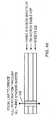
- FIG. 1gives a schematic of one version of the concept, where an axicon optical element 10 and other lenses 11 and 12 are used to focus light rays from a laser 3 (not shown) into a pattern 2b that will have a linear shape, parallel to the optical axis of the system.
- the substrate 1is positioned so that it is within the line-focus. With a line-focus of about 1 mm extent, and a picosecond laser that produces output power greater than or equal to about 20 W at a repetition rate of 100 kHz (about 200 micro Joules/burst measured at the material), then the optical intensities in the line region 2b can easily be high enough to create non-linear absorption in the material.
- the pulsed laser beamcan have an average laser burst energy measured, at the material, greater than 40 microJoules per mm thickness of material.
- the average laser burst energy usedcan be as high as 2500 ⁇ J per mm of thickness of material, for example 100-2000 ⁇ J/mm, with 200-1750 ⁇ J/mm being preferable, and 500-1500 ⁇ J/mm being more preferable.
- This "average laser energy”can also be referred to as an average, per-burst, linear energy density, or an average energy per laser burst per mm thickness of material.
- the burst energy densitycan be in a range from about 25 ⁇ J/mm of line focus to about 125 ⁇ J/mm of line focus, or in a range from about 75 ⁇ J/mm of line focus to about 125 ⁇ J/mm of line focus.
- a region of damaged, ablated, vaporized, or otherwise modified materialis created that approximately follows the linear region of high intensity.
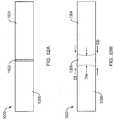
- a method of laser processing a materialincludes focusing a pulsed laser beam 2 into a laser beam focal line 2b oriented along the beam propagation direction.
- laser 3(not shown) emits laser beam 2, which has a portion 2a incident to the optical assembly 6.
- the optical assembly 6turns the incident laser beam into an extensive laser beam focal line 2b on the output side over a defined expansion range along the beam direction (length 1 of the focal line).
- the planar substrate 1is positioned in the beam path to at least partially overlap the laser beam focal line 2b of laser beam 2. The laser beam focal line is thus directed into the substrate.
- Reference 1adesignates the surface of the planar substrate facing the optical assembly 6 or the laser, respectively, and reference 1b designates the reverse surface of substrate 1.
- the substrate or material thickness(in this embodiment measured perpendicularly to the planes 1a and 1b, i.e., to the substrate plane) is labeled with d.
- the substrate or materialcan be a glass article that is substantially transparent to the wavelength of the laser beam 2, for example.
- substrate 1(or material or glass article) is aligned perpendicular to the longitudinal beam axis and thus behind the same focal line 2b produced by the optical assembly 6 (the substrate is perpendicular to the plane of the drawing).
- the focal linebeing oriented or aligned along the beam direction, the substrate is positioned relative to the focal line 2b in such a way that the focal line 2b starts before the surface 1a of the substrate and stops before the surface 1b of the substrate, i.e. still focal line 2b terminates within the substrate and does not extend beyond surface 1b.
- the focal line 2bstarts before the surface 1a of the substrate and stops before the surface 1b of the substrate, i.e. still focal line 2b terminates within the substrate and does not extend beyond surface 1b.
- the extensive laser beam focal line 2bgenerates (assuming suitable laser intensity along the laser beam focal line 2b, which intensity is ensured by the focusing of laser beam 2 on a section of length 1, i.e. a line focus of length 1) an extensive section 2c (aligned along the longitudinal beam direction) along which an induced absorption is generated in the substrate material.
- the induced absorptionproduces defect line formation in the substrate material along section 2c.
- the defect lineis a microscopic (e.g., >100 nm and ⁇ 0.5 micron in diameter) elongated "hole" (also called a perforation, a damage track, or a defect line) in a substantially transparent material, substrate, or workpiece generated by using a single high energy burst pulse.
- Individual perforationscan be created at rates of several hundred kilohertz (several hundred thousand perforations per second), for example. With relative motion between the source and the material, these perforations can be placed adjacent to one another (spatial separation varying from sub-micron to many microns as desired). This spatial separation (pitch) can be selected to facilitate separation of the material or workpiece.
- the defect line/damage trackis a "through hole", which is a hole or an open channel that extends from the top to the bottom of the substantially transparent material.
- the damage trackis not a true "through hole” because there are particles of the material block the path of the damage track.
- the damage trackcan extend from the top surface to the bottom surface of material, in some embodiments it is not a continuous hole or channel because particles of the material are blocking the path.
- the defect line/damage track formationis not only local, but over the entire length of the extensive section 2c of the induced absorption.
- the length of section 2c(which corresponds to the length of the overlapping of laser beam focal line 2b with substrate 1) is labeled with reference L.
- the average diameter or extent of the section of the induced absorption 2c(or the sections in the material of substrate 1 undergoing the defect line formation) is labeled with reference D.
- This average extent Dbasically corresponds to the average diameter ⁇ of the laser beam focal line 2b, that is, an average spot diameter in a range of between about 0.1 micron and about 5 microns.
- a microscopici.e., ⁇ 2 micron and >100 nm in diameter, and in some embodiments ⁇ 0.5 ⁇ m and >100 nm
- elongated "hole”also called a perforation, a damage track, or a defect line, as noted above
- These individual perforationscan be created at rates of several hundred kilohertz (several hundred thousand perforations per second, for example).
- these perforationscan be placed at any desired location within the workpiece.
- the defect line/damage trackis a "through hole", which is a hole or an open channel that extends from the top to the bottom of the transparent material.
- the defect line/damage trackmay not be a continuous channel, and may be blocked or partially blocked by portions or sections of solid material (e.g., glass).
- the internal diameter of the defect line/damage trackis the internal diameter of the open channel or the air hole.
- the internal diameter of the defect line/damage trackis ⁇ 500 nm, for example ⁇ 400 nm, or ⁇ 300 nm.
- the disrupted or modified area (e.g, compacted, melted, or otherwise changed) of the material surrounding the holes in the embodiments disclosed hereinpreferably has diameter of ⁇ 50 microns (e.g,, ⁇ 10 micron).
- the substrate material(which is transparent to the wavelength ⁇ of laser beam 2) is heated due to the induced absorption along the focal line 2b arising from the nonlinear effects associated with the high intensity of the laser beam within focal line 2b.
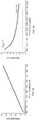
- FIG. 2Billustrates that the heated substrate material will eventually expand so that a corresponding induced tension leads to micro-crack formation, with the tension being the highest at surface 1a.
- MPAmulti-photon absorption
- MPAis the simultaneous absorption of two or more photons of identical or different frequencies in order to excite a molecule from one state (usually the ground state) to a higher energy electronic state (possibly resulting in ionization).
- the energy difference between the involved lower and upper states of the moleculecan be equal to the sum of the energies of the two or more photons.
- MPAalso called induced absorption, can be a second-order, third-order, or higher-order process, for example, that is several orders of magnitude weaker than linear absorption.
- MPAdiffers from linear absorption in that the strength of induced absorption can be proportional to the square, or the cube, or other higher power, of the light intensity, for example, instead of being proportional to the light intensity itself.
- MPAis a nonlinear optical process.
- optical assemblies 6, which can be applied to generate the focal line 2b, as well as a representative optical setup, in which these optical assemblies can be applied,are described below. All assemblies or setups are based on the description above so that identical references are used for identical components or features or those which are equal in their function. Therefore only the differences are described below.
- the individual focal lines positioned on the substrate surfaceshould be generated using the optical assembly described below (hereinafter, the optical assembly is alternatively also referred to as laser optics).
- the optical assemblyis alternatively also referred to as laser optics.
- the optical assemblyIn order to achieve a small spot size of, for example, 0.5 micron to 2 microns in case of a given wavelength ⁇ of laser 3 (interaction with the material of substrate 1), certain requirements must usually be imposed on the numerical aperture of laser optics 6.
- the laser beammust illuminate the optics up to the required aperture, which is typically achieved by means of beam widening using widening telescopes between the laser and focusing optics.
- the spot sizeshould not vary too strongly for the purpose of a uniform interaction along the focal line. This can, for example, be ensured (see the embodiment below) by illuminating the focusing optics only in a small, circular area so that the beam opening and thus the percentage of the numerical aperture only vary slightly.
- FIG. 3Asection perpendicular to the substrate plane at the level of the central beam in the laser beam bundle of laser radiation 2; here, too, laser beam 2 is perpendicularly incident to the substrate plane, i.e. incidence angle is 0° so that the focal line 2b or the extensive section of the induced absorption 2c is parallel to the substrate normal
- the laser radiation 2a emitted by laser 3is first directed onto a circular aperture 8 which is completely opaque to the laser radiation used.
- Aperture 8is oriented perpendicular to the longitudinal beam axis and is centered on the central beam of the depicted beam bundle 2a.
- the diameter of aperture 8is selected in such a way that the beam bundles near the center of beam bundle 2a or the central beam (here labeled with 2aZ) hit the aperture and are completely absorbed by it. Only the beams in the outer perimeter range of beam bundle 2a (marginal rays, here labeled with 2aR) are not absorbed due to the reduced aperture size compared to the beam diameter, but pass aperture 8 laterally and hit the marginal areas of the focusing optic elements of the optical assembly 6, which, in this embodiment, is designed as a spherically cut, bi-convex lens 7.
- the laser beam focal line 2bis not only a single focal point for the laser beam, but rather a series of focal points for different rays in the laser beam.
- the series of focal pointsform an elongated focal line of a defined length, shown in FIG. 3A as the length 1 of the laser beam focal line 2b.
- Lens 7is centered on the central beam and is designed as a non-corrected, bi-convex focusing lens in the form of a common, spherically cut lens. The spherical aberration of such a lens may be advantageous.
- aspheres or multi-lens systems deviating from ideally corrected systemswhich do not form an ideal focal point but a distinct, elongated focal line of a defined length, can also be used (i.e., lenses or systems which do not have a single focal point).
- the zones of the lensthus focus along a focal line 2b, subject to the distance from the lens center.
- the diameter of aperture 8 across the beam directionis approximately 90% of the diameter of the beam bundle (defined by the distance required for the intensity of the beam to decrease to 1/e 2 of the peak intensity) and approximately 75% of the diameter of the lens of the optical assembly 6.
- FIG. 3Ashows the section in one plane through the central beam, and the complete three-dimensional bundle can be seen when the depicted beams are rotated around the focal line 2b.
- This type of focal lineis that the conditions (spot size, laser intensity) may vary along the focal line (and thus along the desired depth in the material) and therefore the desired type of interaction (no melting, induced absorption, thermal-plastic deformation up to crack formation) may possibly occur only in selected portions of the focal line. This means in turn that possibly only a part of the incident laser light is absorbed by the substrate material in the desired way. In this way, the efficiency of the process (required average laser power for the desired separation speed) may be impaired, and the laser light may also be transmitted into undesired regions (parts or layers adherent to the substrate or the substrate holding fixture) and interact with them in an undesirable way (e.g. heating, diffusion, absorption, unwanted modification).
- FIGs. 3B-1-4show (not only for the optical assembly in FIG. 3A , but basically also for any other applicable optical assembly 6) that the position of laser beam focal line 2b can be controlled by suitably positioning and/or aligning the optical assembly 6 relative to substrate 1 as well as by suitably selecting the parameters of the optical assembly 6.
- the length 1 of the focal line 2bcan be adjusted in such a way that it exceeds the substrate thickness d (here by factor 2). If substrate 1 is placed (viewed in longitudinal beam direction) centrally to focal line 2b, an extensive section of induced absorption 2c is generated over the entire substrate thickness.
- the laser beam focal line 2bcan have a length 1 in a range of between about 0.01 mm and about 100 mm or in a range of between about 0.1 mm and about 10 mm, for example.
- Various embodimentscan be configured to have length 1 of about 0.1 mm, 0.2 mm, 0.3 mm, 0.4 mm, 0.5 mm, 0.7 mm, 1 mm, 2 mm, 3 mm or 5 mm, for example.
- a focal line 2b of length 1is generated which corresponds more or less to the substrate thickness d. Since substrate 1 is positioned relative to line 2b in such a way that line 2b starts at a point outside the substrate, the length L of the extensive section of induced absorption 2c (which extends here from the substrate surface to a defined substrate depth, but not to the reverse surface 1b) is smaller than the length 1 of focal line 2b.
- FIG. 3B-3shows the case in which the substrate 1 (viewed along a direction perpendicular to the beam direction) is positioned above the starting point of focal line 2b so that, as in FIG.
- the length 1 of line 2bis greater than the length L of the section of induced absorption 2c in substrate 1.
- the focal linethus starts within the substrate and extends beyond the reverse surface 1b.
- focal line 2bit is particularly advantageous to position the focal line 2b in such a way that at least one of surfaces 1a, 1b is covered by the focal line, so that the section of induced absorption 2c starts at least on one surface of the substrate. In this way it is possible to achieve virtually ideal cuts or formation of damage tracks while avoiding ablation, feathering and particulation at the surface.
- FIG. 4depicts another applicable optical assembly 6.
- the basic constructionfollows the one described in FIG. 3A so that only the differences are described below.
- the depicted optical assemblyis based the use of optics with a non-spherical free surface in order to generate the focal line 2b, which is shaped in such a way that a focal line of defined length 1 is formed.
- aspherescan be used as optic elements of the optical assembly 6.
- a so-called conical prismalso often referred to as axicon
- An axiconis a special, conically cut lens which forms a spot source on a line along the optical axis (or transforms a laser beam into a ring).
- the layout of such an axiconis generally known to one skilled in the art; the cone angle in the example is 10°.
- the apex of the axicon labeled here with reference 9is directed towards the incidence direction and centered on the beam center. Since the focal line 2b produced by the axicon 9 starts within its interior, substrate 1 (here aligned perpendicularly to the main beam axis) can be positioned in the beam path directly behind axicon 9. As FIG. 4 shows, it is also possible to shift substrate 1 along the beam direction due to the optical characteristics of the axicon while remaining within the range of focal line 2b. The section of the induced absorption 2c in the material of substrate 1 therefore extends over the entire substrate depth d.
- the depicted layoutis subject to the following restrictions: Since the region of focal line 2b formed by axicon 9 begins within axicon 9, a significant part of the laser energy is not focused into the section of induced absorption 2c of focal line 2b, which is located within the material, in the situation where there is a separation a between axicon 9 and the substrate or glass composite workpiece material. Furthermore, length 1 of focal line 2b is related to the beam diameter through the refractive indices and cone angles of axicon 9. This is why, in the case of relatively thin materials (several millimeters), the total focal line is much longer than the substrate or glass composite workpiece thickness, having the effect that much of the laser energy is not focused into the material.
- FIG. 5Adepicts such an optical assembly 6 in which a first optical element with a non-spherical free surface designed to form an extensive laser beam focal line 2b is positioned in the beam path of laser 3.
- this first optical elementis an axicon 10 with a cone angle of 5°, which is positioned perpendicularly to the beam direction and centered on laser beam 3. The apex of the axicon is oriented towards the beam direction.
- a second, focusing optical elementhere the plano-convex lens 11 (the curvature of which is oriented towards the axicon), is positioned in the beam direction at a distance z1 from the axicon 10.
- the distance z1in this case approximately 300 mm, is selected in such a way that the laser radiation formed by axicon 10 is circularly incident on the outer radial portion of lens 11.
- Lens 11focuses the circular radiation on the output side at a distance z2, in this case approximately 20 mm from lens 11, on a focal line 2b of a defined length, in this case 1.5 mm.
- the effective focal length of lens 11is 25 mm in this embodiment.
- the circular transformation of the laser beam by axicon 10is labeled with the reference SR.
- FIG. 5Bdepicts the formation of the focal line 2b or the induced absorption 2c in the material of substrate 1 according to FIG. 5A in detail.
- the optical characteristics of both elements 10, 11 as well as the positioning of themis selected in such a way that the length 1 of the focal line 2b in beam direction is exactly identical with the thickness d of substrate 1. Consequently, an exact positioning of substrate 1 along the beam direction is required in order to position the focal line 2b exactly between the two surfaces 1a and 1b of substrate 1, as shown in FIG. 5B .
- the focal lineis formed at a certain distance from the laser optics, and if the greater part of the laser radiation is focused up to a desired end of the focal line.
- thiscan be achieved by illuminating a primarily focusing element 11 (lens) only circularly (annularly) over a particular outer radial region, which, on the one hand, serves to realize the required numerical aperture and thus the required spot size, and, on the other hand, however, the circle of diffusion diminishes in intensity after the required focal line 2b over a very short distance in the center of the spot, as a basically circular spot is formed. In this way, the defect line/damage track formation is stopped within a short distance in the required substrate depth.
- a combination of axicon 10 and focusing lens 11meets this requirement.
- the axiconacts in two different ways: due to the axicon 10, a usually round laser spot is sent to the focusing lens 11 in the form of a ring, and the asphericity of axicon 10 has the effect that a focal line is formed beyond the focal plane of the lens instead of a focal point in the focal plane.
- the length 1 of focal line 2bcan be adjusted via the beam diameter on the axicon.
- the numerical aperture along the focal lineon the other hand, can be adjusted via the distance z1 axicon-lens and via the cone angle of the axicon. In this way, the entire laser energy can be concentrated in the focal line.
- the circular (annular) illuminationstill has the advantage that (1) the laser power is used optimally in the sense that most of the laser light remains concentrated in the required length of the focal line and (2) it is possible to achieve a uniform spot size along the focal line - and thus a uniform separation of part from substrate along the focal line - due to the circularly illuminated zone in conjunction with the desired aberration set by means of the other optical functions.
- the focal length f of the collimating lens 12is selected in such a way that the desired circle diameter dr results from distance zla from the axicon to the collimating lens 12, which is equal to f.
- the desired width br of the ringcan be adjusted via the distance zlb (collimating lens 12 to focusing lens 11). As a matter of pure geometry, the small width of the circular illumination leads to a short focal line. A minimum can be achieved at distance f.
- the optical assembly 6 depicted in FIG. 5Ais thus based on the one depicted in FIG. 1 so that only the differences are described below.
- the collimating lens 12, here also designed as a plano-convex lens (with its curvature towards the beam direction)is additionally placed centrally in the beam path between axicon 10 (with its apex towards the beam direction), on the one side, and the plano-convex lens 11, on the other side.
- the distance of collimating lens 12 from axicon 10is referred to as zla, the distance of focusing lens 11 from collimating lens 12 as zlb, and the distance of the focal line 2b from the focusing lens 11 as z2 (always viewed in beam direction).
- the circular radiation SR formed by axicon 10which is incident divergently and under the circle diameter dr on the collimating lens 12, is adjusted to the required circle width br along the distance zlb for an at least approximately constant circle diameter dr at the focusing lens 11.
- a very short focal line 2bis intended to be generated so that the circle width br of approximately 4 mm at lens 12 is reduced to approximately 0.5 mm at lens 11 due to the focusing properties of lens 12 (circle diameter dr is 22 mm in the example).
- Burstingis a type of laser operation where the emission of pulses is not in a uniform and steady stream but rather in tight clusters of pulses. This is depicted in FIG. 6 .
- Each "burst" 610may contain multiple pulses 620 (such as at least 2 pulses, at least 3 pulses, at least 4 pulses, at least 5 pulses, at least 10 pulses, at least 15 pulses, at least 20 pulses, or more) of very short duration .
- Pulses 610can have a pulse duration T d in a range from about 0.1 psec to about 100 psec (for example, 0.1 psec, 5 psec, 10 psec, 15 psec, 18ps, 20 ps, 22 ps, 25 ps, 30 ps, 50 ps, 75 ps, or therebetween).
- the pulse durationcan be in a range from greater than about 1 picosecond and less than about 100 picoseconds or greater than about 5 picoseconds and less than about 20 picoseconds.
- These individual pulses 620 within a single burst 610can also be termed "sub-pulses,” which simply denotes the fact that they occur within a single burst of pulses.
- the energy or intensity of each laser pulse 620 within the burst 610may not be equal to that of other pulses within the bust, and the intensity distribution of the multiple pulses within a burst 610 often follows an exponential decay in time governed by the laser design.
- each pulse 620 within the burst 610is separated in time by a duration T p in a range of between about 1 nsec and about 50 nsec, (e.g. 10-50 ns, or 10-50ns, or 10-30 nsec), with the time often governed by the laser cavity design.
- T pthe time separation between each pulses (pulse -to- pulse separation) within a burst 610 is relatively uniform ( ⁇ 10%).
- T pis approximately 20 nsec (50 MHz).
- the pulse to pulse separation T p within a burstis maintained within about ⁇ 10%, or is about ⁇ 2 nsec.
- the time between each "burst" 610 of pulses 620i.e., time separation T b between bursts
- T bis about 10 microseconds, for a laser repetition rate of about 100 kHz.
- T bcan be around 5 microseconds for a laser repetition rate or frequency of about 200 kHz.
- the time between each "burst"can also be around 5 microseconds, for a laser repetition rate of ⁇ 200 kHz, for example.
- the laser repetition rateis also referred to as burst repetition frequency herein, and is defined as the time between the first pulse in a burst to the first pulse in the subsequent burst.
- the burst repetition frequencyis in a range of between about 1 kHz and about 4 MHz. More preferably, the laser repetition rates can be in a range of between about 10 kHz and 650 kHz.
- the laser repetition ratecan be about 10 kHz or greater or about 100 kHz or greater.
- the time T b between the first pulse in each burst to the first pulse in the subsequent burstmay be 0.25 microsecond (4MHz repetition rate) to 1000 microseconds (1kHz repetition rate), for example 0.5 microseconds (2MHz repetition rate) to 40 microseconds (25kHz repetition rate), or 2 microseconds (500kHz repetition rate) to 20 microseconds (50kHz repetition rate).
- the exact timings, pulse durations, and repetition ratescan vary depending on the laser design, but short pulses (T d ⁇ 20 psec and preferably T d ⁇ 15 psec) of high intensity have been shown to work particularly well. In some of the embodiments 5 psec ⁇ T d ⁇ 15 psec.
- the required energy to modify the materialcan be described in terms of the burst energy - the energy contained within a burst (each burst 610 contains a series of pulses 620), or in terms of the energy contained within a single laser pulse (many of which may comprise a burst).
- the energy per burstcan be from 25 ⁇ J-750 ⁇ J, more preferably 40 ⁇ J-750 ⁇ J, 50 ⁇ J -500 ⁇ J, 50-250 ⁇ J, or 100-250 ⁇ J.
- the energy of an individual pulse within the burstcan be less, and the exact individual laser pulse energy will depend on the number of pulses within the burst and the rate of decay (e.g.
- each individual laser pulsewill contain less energy than if the same burst had only 2 individual laser pulses.
- a laser capable of generating such bursts of pulsesis advantageous for such processing.
- the use of a burst sequence that spreads the laser energy over a rapid sequence of sub-pulses (that comprise a burst)allows access to larger timescales of high intensity interaction with the material than is possible with single-pulse lasers.
- a single-pulsecan be expanded in time, as this is done the intensity within the pulse must drop as roughly one over the pulse width. Hence if a 10 psec pulse is expanded to a 10 nsec pulse, the intensity drop by roughly three orders of magnitude.
- the intensity during each sub-pulsecan remain very high - for example three 10 psec pulses spaced apart in time by approximately 10 nsec still allows the intensity within each pulse to be approximately within a factor of three of a single 10 psec pulse, while the laser is allowed to interact with the material over a timescale that is now three orders of magnitude larger.
- This adjustment of multiple pulses within a burstthus allows manipulation of time-scale of the laser-material interaction in ways that can facilitate greater or lesser light interaction with a pre-existing plasma plume, greater or lesser light-material interaction with atoms and molecules that have been pre-excited by an initial or previous laser pulse.
- the damage track or holeis formed in the material when a single burst of pulses strikes substantially the same location on the material. That is, multiple laser pulses within a single burst correspond to a single defect line or a hole location in the material.
- the individual pulses within the burstcannot be at exactly the same spatial location on the material.
- the pulsesare well within 1 micron of one another so that they strike the material at essentially the same location. For example, the pulses may strike the material at a spacing sp where 0 ⁇ sp ⁇ 500 nm from one another.
- the spacing spis in a range from about 1 nm to about 250 nm or from about 1 nm to about 100 nm.
- the optical method of forming the line focuscan take multiple forms, using donut shaped laser beams and spherical lenses, axicon lenses, diffractive elements, or other methods to form the linear region of high intensity as described above.
- the type of laser (picosecond, femtosecond, etc.) and wavelength (IR, green, UV, etc.)can also be varied, as long as sufficient optical intensities are reached to create breakdown of the substrate material.
- the damage tracks created by the aforementioned laser processgenerally take the form of holes with interior dimensions in the range of about 0.1 microns to 2 microns, for example 0.1-1.5 microns.
- the holes formed by the laserare very small (single microns or less) in dimension-i.e., they are narrow. In some embodiments, these holes are 0.2 to 0.7 microns in diameter.
- the damage tracksare not continuous holes or channels.
- the diameter of the damage trackscan be 5 microns or less, 4 microns or less, 3 microns or less, 2 microns or less, or 1 micron or less.
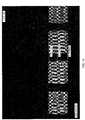
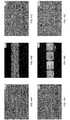
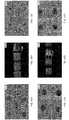
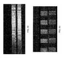
- the diameter of the damage trackscan be in a range from greater than 100 nm to less than 2 microns, or from greater than 100 nm to less than 0.5 microns. Scanning electron micrograph images of such features are shown in FIGS. 7A and 7B . These holes are un-etched holes (i.e., they have not been widened by the etching steps)
- the holes or defect lines/damage trackscan perforate the entire thickness of the material, and may or may not be a continuous opening throughout the depth of the material.
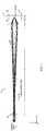
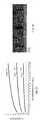
- FIG. 8shows an example of such tracks or defect lines perforating the entire thickness of a workpiece of 150 micron thick Eagle XG® glass substrate.
- the perforations or damage tracksare observed through the side of a cleaved edge.
- the tracks through the materialare not necessarily through holes. There are often regions of glass that plug the holes, but they are generally small in size, on the order of microns, for example.
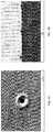
- FIG. 9shows a greater magnification image of similar holes or damage tracks, where the diameter of the holes can be more clearly seen, and also the presence of regions where the hole is plugged by remaining glass.
- the tracks made through the glassare about 1 micron in diameter. They are not completely open - i.e., regions of material are removed, but complete through-holes are not necessarily formed.
- the focal line lengthneeds to be longer than the stack height.
- the testswere performed with three stacked 150 micron sheets of Eagle XG® glass, and full perforations were made through all three pieces with the perforations or defect lines/damage tracks (of approximately 1 micron internal diameter) extended from the top surface of the upper sheet all the way through the bottom surface of the bottom sheet.
- An example of a focal line configured for full perforation through a single substrateis shown in FIG. 3B-1 , while a full perforation through three stacked sheets is described hereinafter in conjunction with FIG. 48 .
- the internal diameter of a defect line or perforationis the internal diameter of the open channel or the air hole.
- the disrupted or modified area (e.g, compacted, melted, or otherwise changed) of the material surrounding the holes in thecan have a diameter larger than the internal diameter of the open channel or air hole.
- the perforations in the stackcan be acid etched to create a plurality of through holes that extend through all of the glass sheets comprising the stack, or alternatively the glass sheets can be separated and then the holes can be acid etched in each of the sheets separately.
- this processmay result in glass with etched hole diameters of 1-100 microns, for example, 10-75 microns, 10-50 microns, 2-25 microns, 2-20 microns, 2-15 microns, 2-10 microns, and the holes may have, for example, spacing of 25-1000 microns.
- This processmay also be utilized to create holes in sheets of transparent materials other than glass. Since the optical system uses a line focus, it is possible to drill through transparent materials that have large (>1 micron, up to 4mm, for example 10-500 microns) air gaps or other filler materials (e.g. water, transparent polymers, transparent electrodes like indium tin oxide) between the substrate sheets.
- air gaps or other filler materialse.g. water, transparent polymers, transparent electrodes like indium tin oxide
- the ability to continue to drill through multiple glass sheets even when they are separated by a macroscopic (many microns, many tens of microns, or even many hundreds of microns)is to be noted as a particular advantage of this line focus method of drilling.
- the critical power to self-focus in airis ⁇ 20X as much as the critical power required in glass, making such an air gap very problematic.
- the beamwill continue to form a high intensity core whether or not the glass material is there, or polymer, or an air gap, or even in the presence of a vacuum.
- the line focus beamwill have no trouble continuing to drill the glass layer underneath regardless of the gap in material between it and the glass sheet above.
- the stack of substrate sheetsmay contain substrates of different glass compositions throughout the stack.
- one stackmay contain both substrate sheets of Eagle XG glass and of Corning glass code 2320.
- the stack of transparent substrate sheetsmay contain non-glass transparent inorganic material such as sapphire.
- the substratesmust be substantially transparent to the wavelength of the laser that is used to create the line focus, for example the laser wavelength being situated from 200nm to 2000nm, for example, 1064 nm, 532 nm, 355 nm, or 266 nm.
- the substratecan also be transparent to at least one wavelength in a range from about 390 nm to about 700 nm.
- the substratecan transmit at least 70%, at least 75%, at least 80%, at least 85%, or at least 90% of at least one wavelength in a range from about 390 nm to about 700 nm.
- Drilling holes/damage tracks in glass or other transparent materialscan be used to create an article comprising a stack of substrates (spaced or in direct contact with one another) with a plurality of holes formed through said stack, where the holes extend through each of the substrates, the holes being, for example, between 1-100 microns in diameter, and, for example, having a spacing of 25-1000 microns.
- this processcan be utilized to create a substantially transparent article comprising a multilayer stack, where the multilayer stack comprises multiple glass layers and at least one layer of polymer situated between the glass layers, or at least two glass layers of different compositions, or at least one glass layer and at least on non-glass inorganic layer.
- the lateral spacing (pitch) between the holes or defect lines/damage tracksis determined by the pulse or burst rate of the laser as the substrate is translated underneath the focused laser beam. Only a single picosecond laser pulse burst is usually necessary to form an entire hole, but multiple bursts may be used if desired.
- the lasercan be triggered to fire at longer or shorter intervals. In some embodiments, the laser triggering generally can be synchronized with the stage driven motion of the workpiece beneath the beam, so laser bursts are triggered at a fixed interval, such as every 1 micron, every 5 microns, every 10 microns, or every 20 microns or greater.
- the distance, or periodicity, between adjacent damage trackscan depend upon the desired pattern of through-holes (i.e., the holes formed after the etching process).
- the desired pattern of damage tracks (and the resultant through-holes that are formed therefrom after etching)is an aperiodic pattern of irregular spacing. They need to be at locations where traces will be laid on the interposer or where specific electrical connections on the interposer to the chips are going to be placed. Therefore, a distinction between cutting and damage track drilling for interposers is that the through-holes for interposers is laid out in aperiodic patterns.
- the damage tracksare made at a specific periodic pitch where the pitch depends on the composition of the material being cut.
- the holes or defect linescan have a spacing between adjacent holes/defect lines/damage tracks of about 10 ⁇ m or greater, about 20 ⁇ m or greater, about 30 ⁇ m or greater, about 40 ⁇ m or greater, about 50 ⁇ m or greater.
- the spacingcan be up to about 20 mm.
- the spacingcan be from 50 microns to 500 microns or from 10 microns and 50 microns.
- FIG. 10shows a similar sample, in this case 300 micron thick Corning Eagle XG® glass, from a top view, with a periodic array of holes.
- the entrance points of the laser beamare clearly seen.
- the pitch or spacing between adjacent holesis 300 microns, and the approximate diameter of the holes is 2 microns, with a rim or modified or raised material around each hole of about 4 microns diameter.
- a variety of laser process parameterswere explored to find conditions that produced holes that fully penetrated the material and had minimal micro-cracking of the glass.
- the laser power and lens focal length(which determines the focal line length and hence power density) are particularly important parameters to ensure full penetration of the glass and low micro-cracking.
- FIG. 11shows a result where significant micro-cracking of the glass occurred.
- FIG. 12An example of laser formed blind holes is shown in FIG. 12 .
- the damage tracksextend about 75% of the way through the glass.
- the focus of the opticsis raised up until the line focus only causes damage in the top section of the glass.
- Other blind hole depthsmay be realized, such as extending only 10% of the way through the glass, only 25%, only 50%, or any fractional value of the glass thickness.
- the laser triggeringgenerally is synchronized with the stage driven motion of the part beneath the beam, and laser pulses are most often triggered at a fixed interval, such as every 1 micron, or every 5 microns.
- the exact spacingis determined by the material properties that facilitate crack propagation from perforated hole to perforated hole, given the stress level in the substrate.
- the holesare generally separated by much greater distance than required for cutting - instead of a pitch of about 10 microns or less, the spacing between holes can be hundreds of microns.
- the exact locations of the holesneed not be at regular intervals (i.e., they are aperiodic) - the location simply is determined by when the laser is triggered to fire, and may be at any location within the part.
- the holes made in FIG. 9are an example of spacing and pattern that are somewhat representative of interposer applications.
- process speedis generally not limited directly by laser power, but more by the ability to direct the already abundant laser pulses or bursts to the specific locations at which holes are needed.
- the desired pattern of damage tracks(and the resultant through-holes that are formed therefrom after etching) is an aperiodic pattern of irregular spacing. They need to be at locations where traces will be laid on the interposer or where specific electrical connections on the interposer to the chips are going to be placed.
- interposersa distinction between cutting and damage track drilling for interposers is that the through-holes for interposers is laid out in aperiodic patterns.
- burst mode psec laserscan readily produce laser bursts of ⁇ 200 microJoules/burst at repetition rates ⁇ 100-200kHz. This corresponds to a time average laser power of about 20-40 Watts.
- to drill interposersmost often the majority of these bursts will be unused, as even with very fast beam deflection methods the beam can only be placed at the desired hole locations at rates of kHz or possibly tens of kHz.
- a primary challenge for efficient drilling with the above line focus and psec pulsed laser processis how the beam is moved and directed across the substrate surface.
- the glass or beamcan then be scanned in a "raster scan" mode where the laser beam travels in the x-direction, scanning across all of the desired hole locations that share common y-axis value. As the beam is scanned, that laser is triggered to fire a burst only at the desired hole locations.
- the substrate or laser beamare moved to a new y-location, the process is repeated for the new set of desired hole locations on this new y-line. This process is then continued until all of the desired holes on the substrate are made.
- the above processis straightforward, but not necessarily efficient as the speed at which the stage and spacing of the desired holes will determine what fraction of laser pulses/bursts can be used. For example, if the laser can produce pulses or bursts at 200,000 bursts/sec, but the stages move at average speed of 0.5m/sec and the holes are on average 100 microns apart, then only about 5,000 bursts/sec are used - about 2.5% of the available laser bursts. While this does drill 5,000 holes (or damage tracks)/sec, this is only a small fraction of the laser capacity.
- Scanning of the glass or beam delivery opticscan be combined with rapid beam deflection available from galvanometer mirrors (galvo) and f-theta lenses, or with piezo actuation of optics or the glass or small ranges, or electro-optic beam deflection (EOD) or acousto-optic beam deflection (AOD), to allow the beam to be rapidly adjusted in a direction orthogonal to the linear "raster" scan direction described above.
- EODelectro-optic beam deflection
- AODacousto-optic beam deflection
- the systemcan now direct the laser beam to any holes within a swath of width dy of the raster scan line.
- Thiscan greatly increase the number of accessible holes by the laser beam per unit time, and thus greatly increase the number of holes/sec that may be drilled.
- the fast beam deflectormay be used not only in a direction perpendicular to the raster scan axis, but also parallel to the scan axis. By also deflecting the beam parallel to the scan axis, the fast beam deflecting component (e.g.
- galvo, AOD, EOD, piezocan be used to allow for holes within a dy swath that have identical scan axis locations (e.g. the x-axis in the above example) but different y-axis locations to be drilled, since the beam can be "moved" backwards relative to the stage scan to drill a second hole at a given x-location without stopping the linear stage motion.
- fast deflection along the scan axisalso allows for more precision in the placement of holes, since it can be used to direct the beam to the desired x-axis location regardless of any small time delays in when the pulsed laser is available to fire a burst, and also compensate for velocity and acceleration artifacts in the linear stage motion.
- the above beam scanning methodsmay also be combined with beam splitting techniques, where a common laser source has its bursts distributed among multiple beam delivery heads above a single substrate or series of substrates.
- an acousto-optic or electro-optic elementsmay be used to deflect every N th pulse to a given optical path, and there may be N optical heads used. This may be accomplished by employing the angle-deflection properties of such beam steering elements, or by using the polarization altering properties of such elements to direct the beams through polarization dependent beam splitters.
- the damage trackscan be created at a speed greater than about 50 damage tracks/second, greater than about 100 damage tracks/second, greater than about 500 damage tracks/second, greater than about 1,000 damage tracks/second, greater than about 2,000 damage tracks/second, greater than about 3,000 damage tracks/second, greater than about 4,000 damage tracks/second, greater than about 5,000 damage tracks/second, greater than about 6,000 damage tracks/second, greater than about 7,000 damage tracks/second, greater than about 8,000 damage tracks/second, greater than about 9,000 damage tracks/second, greater than about 10,000 damage tracks/second, greater than about 25,000 damage tracks/second, greater than about 50,000 damage tracks/second, greater than about 75,000 damage tracks/second, or greater than about 100,000 damage tracks/second.
- acid etchingchanges the holes from a size (for example, about 1 micron) that is too small to practically metalize and use for interposers to more convenient size (for example, 5 microns or higher); 2) etching can take what may start as a non-contiguous hole or simply a damage track through the glass and etch it out to form a continuous though-hole via; 3) etching is a highly parallel process where all of the holes/damage tracks in a part are enlarged at the same time - which is much faster than what would happen if a laser had to re-visit the hole and drill out more material to enlarge it; and 4) etching helps blunt any edges or small checks within the part, increasing the overall strength and reliability of the material.
- FIGs. 52A and 52Billustrate a substrate 1000 after laser drilling and after acid etching, respectively.
- a substrate 1000can be subjected to any of the laser drilling processes described above to form one or more damage tracks or pilot holes 1002 extending from a first or top surface 1004 to a second or bottom surface 1006.
- Damage track 1002is illustrated as being a continuous hole for illustration purposes only. As described above, in some embodiments, damage track 1002 is a non-continuous hole wherein particles of the substrate are present in the damage track. As shown in FIG.
- the damage trackis enlarged to a create a through-hole via 1008, having a top diameter Dt at a top opening in top surface 1004, a bottom diameter Db at a bottom opening in bottom surface 1006, and a waist diameter Dw.
- the waistrefers to the narrowest portion of a hole located between the top and bottom openings. While the profile of through-hole via 1008 is shown as being hourglass shaped due to the waist, this is only exemplary. In some embodiments, the through-hole vias are substantially cylindrical.
- the etching processproduces through-hole vias having a diameter greater than 1 micron, greater than about 2 microns, greater than about 3 microns, greater than about 4 microns, greater than about 5 microns, greater than about 10 microns, greater than about 15 microns, or greater than about 20 microns.
- the acid usedwas 10% HF / 15% HNO 3 by volume.
- the partswere etched for 53 minutes at a temperature of 24-25 °C to remove about 100 microns of material.
- the partswere immersed in this acid bath, and ultrasonic agitation at a combination of 40 kHz and 80 kHz frequencies was used to facilitate penetration of fluid and fluid exchange in the holes/damage tracks.
- manual agitatione.g. mechanical agitation
- of the part within the ultrasonic fieldwas made to prevent standing wave patterns from the ultrasonic field from creating "hot spots" or cavitation related damage on the part, and also to provide macroscopic fluid flow across the part.
- the acid composition and etch ratewas intentionally designed to slowly etch the part - a material removal rate of only 1.9 microns/minute.
- An etch rate of less than, for example, about 2 microns/minuteallows acid to fully penetrate the narrow holes/damage tracks and agitation to exchange fresh fluid and remove dissolved material from the holes/damage tracks which are initially very narrow. This allows the holes to expand during the etch at nearly the same rate throughout the thickness of the substrate (i.e. throughout the length of the hole or damage track).
- the etch ratecan be a rate of less than about 10 microns/min, such as a rate of less than about 5 microns/min, or a rate of less than about 2 microns/min.
- FIGS. 13A and 13Bshow top and bottom views of a resulting part.
- the holesare about 95 microns in diameter, and are very circular, indicating that there was very little micro-cracking of the material.
- the holesare at 300 micron pitch, and each hole is approximately 90-95 microns in diameter.
- the images in FIGS. 13A and 13Bwere taken with a back light, and the bright regions within each hole also indicate that the holes have been fully opened by the acid etching. The same samples were then diced, to look more closely at the interior profiles of the holes.
- FIGS. 15 and 16show the results.
- the holeshave an "hourglass" shape, i.e., they taper down toward the middle of the hole.
- this shapeis determined by the etching environment, rather than the pilot hole formation process.
- the bright areasare the glass; the dark areas are the holes.
- the top (laser incidence) diameter of the holesis about 89 micron diameter, the waist is about 71 microns, and the bottom (laser exit) diameter is about 85 microns.
- FIG. 14shows results of etching a sample that had significant micro-cracking from the laser process - the holes etch out into elongated shapes instead of circular features.
- Micro-crackingcan be reduced by lowering the laser burst energy, increasing the number of pulses per burst, or by increasing the length of the line focus, for example by using a longer focal length objective lens. These changes can lower the energy density contained within the substrate.
- caremust be made to ensure optimal alignment of the optical system such that aberrations are not introduced to the line focus so that azimuthal asymmetries are created in the line focus. Such asymmetries can introduce high energy density locations within the substrate that can lead to micro cracks.
- FIGS. 17A-17CThe results are shown as histograms in FIGS. 17A-17C .
- the top and bottom diametersare both about 95 microns, very close in size, and the standard deviation of about 2.5 microns.
- the waistsare about 70 microns, with a standard deviation of about 3 microns. Thus, the waists are about 30% narrower than the top and bottom diameters.
- Circularityis defined as the maximum diameter of the hole minus the minimum diameter of the same hole, and is given in units of microns.
- the distributionsindicate that the holes are generally circular to less than about 5 microns. There are no significant tails to the distributions that would indicate micro-cracks or chips that have etched out to create non-round shapes.
- the acid etching conditionscan be modified to adjust various attributes of the through-holes to make them useful as via through-holes for an interposer.
- the through-holescan have a top opening, a bottom opening, and a waist, and the ratio of the diameter of the waist to the diameter of the top or bottom opening can be controlled.
- the waistrefers to the narrowest portion of a hole located between the top and bottom openings. Two factors that control the diameter of the waist, top opening, and bottom opening is the etching reaction rate and the diffusion rate.
- the acidIn order to etch away material throughout the thickness of the substrate to enlarge the damage tracks into via through-holes, the acid needs to travel the entire length of the damage track. If the etching rate is too fast so that the acid does not have time to adequately diffuse and reach all portions of the damage track, then the acid will disproportionately etch more material away at the surface of the material than in the middle of the material.
- Manipulation of the Thiele modulus ( ⁇ ) of an etching processas described in Thiele, E.W. Relation between catalytic activity and size of particle, Industrial and Engineering Chemistry, 31 (1939), pp. 916-920 , can be utilized to control the ratio of the waist diameter to the diameter of the top or bottom opening.
- the Thiele moduluswhen the etching reaction time is greater than the diffusion time, the Thiele modulus will be greater than 1. This means that the acid will be depleted before it travels the entire length of the damage track or hole and can be replenished by diffusion in the center of the damage track or hole. As a result, etching will proceed faster at the top and bottom of the tracks or holes at a rate governed by k r and etching at the center will occur more slowly at a rate governed by diffusion leading to an hourglass-like shape for the via hole. However, if the diffusion time is equal to or greater than the etching reaction time, then the Thiele modulus will be less than or equal to 1. Under such conditions, the acid concentration will be uniform along the entire damage track or hole and the damage track or hole will be etched uniformly, yielding a substantially cylindrical via hole.
- the diffusion time and etching reaction timecan be controlled to control the Thiele modulus of the etching system, and thereby the ratio of the waist diameter to the diameters of the top and bottom openings.
- FIG. 53illustrates the relationship between the Thiele modulus of the etching system and an expected percentage of the waist diameter with respect to the diameter of the top and bottom openings.
- the Thiele modulus for the etching processcan be less than or equal to about 5, less than or equal to about 4.5, less than or equal to about 4, less than or equal to about 3.5, less than or equal to about 3, less than or equal to about 2.5, less than or equal to about 2, less than or equal to about 1.5, or less than or equal to about 1.
- the diameter of the waist of the via holeis 50% to 100%, 50% to 95%, 50% to 90%, 50% to 85%, 50% to 80%, 50% to 75%, 50% to 70%, 55% to 100%, 55% to 95%, 55% to 90%, 55% to 85%, 55% to 80%, 55% to 75%, 55% to 70%, 60% to 100%, 60% to 95%, 60% to 60%, 60% to 85%, 60% to 80%, 60% to 75%, 60% to 70%, 65% to 100%, 65% to 95%, 65% to 90%, 65% to 85%, 65% to 80%, 65% to 75%, 65% to 70%, 70% to 100%, 70% to 95%, 70% to 90%, 70% to 85%, 70% to 80%, 70% to 75%, 75% to 100%, 75% to 95%, 75% to 90%, 75% to 85%, 75% to 80%, 80% to 100%, 80% to 95%, 80% to 90%, 80% to 85%, 70% to 80%, 70% to 75%, 75% to 100%, 75% to 95%, 75% to
- the diameter of the waist of the via holeis about 50% or greater, about 55% or greater, about 60% or greater, about 65% or greater, about 70% or greater, about 75% or greater, about 80% or greater, about 85% or greater, about 90% or greater, about 95% or greater, or about 100% of the diameter of the top and/or bottom opening of the via hole.
- the diameter of the waist of the via holeis 50% to 100%, 50% to 95%, 50% to 90%, 50% to 85%, 50% to 80%, 50% to 75%, 50% to 70%, 55% to 100%, 55% to 95%, 55% to 90%, 55% to 85%, 55% to 80%, 55% to 75%, 55% to 70%, 60% to 100%, 60% to 95%, 60% to 60%, 60% to 85%, 60% to 80%, 60% to 75%, 60% to 70%, 65% to 100%, 65% to 95%, 65% to 90%, 65% to 85%, 65% to 80%, 65% to 75%, 65% to 70%, 70% to 100%, 70% to 95%, 70% to 90%, 70% to 85%, 70% to 80%, 70% to 75%, 75% to 100%, 75% to 95%, 75% to 90%, 75% to 85%, 75% to 80%, 80% to 100%, 80% to 95%, 80% to 90%, 80% to 85%, 70% to 80%, 70% to 75%, 75% to 100%, 75% to 95%, 75% to
- the diameter of the waist of the via holeis about 50% or greater, about 55% or greater, about 60% or greater, about 65% or greater, about 70% or greater, about 75% or greater, about 80% or greater, about 85% or greater, about 90% or greater, about 95% or greater, or about 100% of average of the diameter of the top and bottom opening of the via hole.
- FIG. 54illustrates how the Thiele modulus decreases with the initial radius of the damage track.
- FIG. 55illustrates how the Thiele modulus increases with the half-thickness of the substrate.
- the thickness of the substrate and radius of the damage tracksare factors that in some instances cannot be changed if a certain thickness or radius of the damage track is needed. Thus other factors affecting the Thiele modulus can be adjusted in such instances.
- FIG. 56illustrates how the Thiele modulus decreases as the effective diffusivity (D eff ) increases.
- the effective diffusivitycan be increased by adding agitation and/or sonication to the etching conditions as described in more detail below.
- FIG. 57illustrates how the Thiele modulus decreases as the acid concentration decreases, in this example the HF concentration.
- FIG. 57also illustrates how a combination of increasing the effective diffusivity and decreasing the acid concentration decreases the Thiele modulus.
- the etching reaction timecan be controlled by adjusting the acid concentration in the etching solution.
- the etching solutioncan be an aqueous solution including deionized water, a primary acid, and a secondary acid.
- the primary acidcan be hydrofluoric acid and the secondary acid can be nitric acid, hydrochloric acid, or sulfuric acid.
- the etching solutioncan only include a primary acid.
- the etching solutioncan include a primary acid other than hydrofluoric acid and/or a second acid other than nitric acid, hydrochloric acid, or sulfuric acid.
- Exemplary etching solutionscan include 10% by volume hydrofluoric acid/15% by volume nitric acid or 5% by volume hydrofluoric acid/7.5% by volume nitric acid, or 2.5% by volume hydrofluoric acid/3.75% by volume nitric acid.
- orientation of the substrate in the etching tank, mechanical agitation, and/or the addition of surfactant to the etching solutionare other etching conditions that can be modified to adjust the attributes of the via holes.
- the etching solutionis ultrasonically agitated and the substrate is oriented in the etching tank holding the etching solution so that the top and bottom openings of the damage tracks receive substantially uniform exposure to the ultrasonic waves in order for the damage tracks to be etched uniformly.
- the substratecan be oriented in the etching tank so that the surfaces of the substrate with the damage tracks are perpendicular to the bottom of the etching tank rather than parallel to the bottom of the etching tank.
- the etching tankcan be mechanically agitated in the x, y, and z directions to improve uniform etching of the damage tracks.
- the mechanical agitation in the x, y, and z directionscan be continuous.
- a surfactantcan be added to the etching solution to increase the wettability of the damage tracks.
- the increased wettabilitylowers the diffusion time and can allow for increasing the ratio of the diameter of the via hole waist to the diameter of the via hole top and bottom openings.
- the surfactantcan be any suitable surfactant that dissolves into the etching solution and that does not react with the acid(s) in the etching solution.
- the surfactantcan be a fluorosurfactant such as Capstone® FS-50 or Capstone® FS-54.
- the concentration of the surfactant in terms of ml of surfactant/L of etching solutioncan be about 1, about 1.1, about 1.2, about 1.3, about 1.4, about 1.5, about 1.6, about 1.7, about 1.8, about 1.9, about 2 or greater.
- the hole formation ratewas well in excess of 300 holes/sec. If the pattern was made larger in physical extent, so the stage would need to accelerate less often, the average hole formation rate would be faster.
- the laser used herecan easily provide 100,000 pulses/sec at full pulse energy, it is possible to form holes at this rate.
- the limitation for hole formation rateis how fast the laser beam can be moved relative to the substrate. If the holes are spaced 10 microns apart, and the stage speed is 1 m/sec, then 100,000 holes/sec are formed. In fact, this is how cutting of substrates is often done. But for practical interposers the holes are often spaced by hundreds of microns, and at more random intervals (i.e., there is an aperiodic pattern). Hence the numbers stated above for the pattern shown are only about 300 holes/sec. To achieve higher rates, the stage speed can be increased, for example, from 200 mm/sec to 1 m/sec, realizing another 5X increase in speed. Similarly, if the average hole pitch was less than 300 microns, the hole formation rate would increase commensurately.
- the damage trackscan be created at a speed greater than about 50 damage tracks/second, greater than about 100 damage tracks/second, greater than about 500 damage tracks/second, greater than about 1,000 damage tracks/second, greater than about 2,000 damage tracks/second, greater than about 3,000 damage tracks/second, greater than about 4,000 damage tracks/second, greater than about 5,000 damage tracks/second, greater than about 6,000 damage tracks/second, greater than about 7,000 damage tracks/second, greater than about 8,000 damage tracks/second, greater than about 9,000 damage tracks/second, greater than about 10,000 damage tracks/second, greater than about 25,000 damage tracks/second, greater than about 50,000 damage tracks/second, greater than about 75,000 damage tracks/second, or greater than about 100,000 damage tracks/second.
- the viascan have a diameter of about 30 microns or less, about 25 microns or less, about 20 microns or less, about 15 microns or less, about 10 microns or less, in a range from about 5 to about 10 microns, about 5 to about 15 microns, about 5 to about 20 microns, about 5 to about 25 microns, about 5 to about 30 microns, or up to many tens of microns depending upon requirements for the intended use. In other embodiments, the vias can have a diameter of greater than about 20 ⁇ m.
- the substratecan have vias with varying diameter, for example the vias can have a difference of at least 5 ⁇ m in diameter.
- a difference in the diameter of the top opening and the bottom opening of the viascan be 3 ⁇ m or less, 2.5 ⁇ m or less, 2 ⁇ m or less, 1.5 ⁇ m or less or 1 ⁇ m or less, which can be enabled by the use of a line focus beam to create damage tracks in the material. These damage tracks maintain a very small diameter over the entire depth of the substrate, which is what ultimately yields uniform top and bottom diameters after etching.
- the spacing (center to center distance) between adjacent the viascan be about 10 ⁇ m or greater, about 20 ⁇ m or greater, about 30 ⁇ m or greater, about 40 ⁇ m or greater, about 50 ⁇ m or greater. In some embodiments, the spacing of adjacent vias can be up to about 20 mm.
- the density of the viascan about 0.01 vias/mm 2 or greater, about 0.1 vias/mm 2 or greater, about 1 via/mm 2 or greater, about 5 vias/mm 2 or greater, about 10 vias/mm 2 or greater, about 20 vias/mm 2 or greater, about 30 vias/mm 2 or greater, about 40 vias/mm 2 or greater, about 50 vias/mm 2 or greater, about 75 vias/mm 2 or greater, about 100 vias/mm 2 or greater, about 150 vias/mm 2 or greater, about 200 vias/mm 2 or greater, about 250 vias/mm 2 or greater, about 300 vias/mm 2 or greater, about 350 vias/mm 2 or greater, about 400 vias/mm 2 or greater, about 450 vias/mm 2 or greater, about 500 vias/mm 2 or greater, about 550 vias/mm 2 or greater, about 600 vias/mm 2 or greater, or about 650 vias/mm 2 or greater. In some embodiments, the density of the vias can range from about 0.01 vias/mm 2
- the diameter of the waist of the via holeis 50% to 100%, 50% to 95%, 50% to 90%, 50% to 85%, 50% to 80%, 50% to 75%, 50% to 70%, 55% to 100%, 55% to 95%, 55% to 90%, 55% to 85%, 55% to 80%, 55% to 75%, 55% to 70%, 60% to 100%, 60% to 95%, 60% to 60%, 60% to 85%, 60% to 80%, 60% to 75%, 60% to 70%, 65% to 100%, 65% to 95%, 65% to 90%, 65% to 85%, 65% to 80%, 65% to 75%, 65% to 70%, 70% to 100%, 70% to 95%, 70% to 90%, 70% to 85%, 70% to 80%, 70% to 75%, 75% to 100%, 75% to 95%, 75% to 90%, 75% to 85%, 75% to 80%, 80% to 100%, 80% to 95%, 80% to 100%, 80% to 95%, 80% to 90%, 80% to 85%, 85%, 85% to 65% to 80%,
- the diameter of the waist of the via holeis about 50% or greater, about 55% or greater, about 60% or greater, about 65% or greater, about 70% or greater, about 75% or greater, about 80% or greater, about 85% or greater, about 90% or greater, about 95% or greater, or about 100% of the diameter of the top and/or bottom opening of the via hole.
- the diameter of the waist of the via holeis 50% to 100%, 50% to 95%, 50% to 90%, 50% to 85%, 50% to 80%, 50% to 75%, 50% to 70%, 55% to 100%, 55% to 95%, 55% to 90%, 55% to 85%, 55% to 80%, 55% to 75%, 55% to 70%, 60% to 100%, 60% to 95%, 60% to 60%, 60% to 85%, 60% to 80%, 60% to 75%, 60% to 70%, 65% to 100%, 65% to 95%, 65% to 90%, 65% to 85%, 65% to 80%, 65% to 75%, 65% to 70%, 70% to 100%, 70% to 95%, 70% to 90%, 70% to 85%, 70% to 80%, 70% to 75%, 75% to 100%, 75% to 95%, 75% to 90%, 75% to 85%, 75% to 80%, 80% to 100%, 80% to 95%, 80% to 90%, 80% to 85%, 70% to 80%, 70% to 75%, 75% to 100%, 75% to 95%, 75% to
- the diameter of the waist of the via holeis about 50% or greater, about 55% or greater, about 60% or greater, about 65% or greater, about 70% or greater, about 75% or greater, about 80% or greater, about 85% or greater, about 90% or greater, about 95% or greater, or about 100% of the average diameter of the top and bottom opening of the via hole.
- an aspect ratio (substrate thickness:via diameter) of the via holescan be about 1:1 or greater, about 2:1 or greater, about 3:1 or greater, about 4:1 or greater, about 5:1 or greater, about 6:1 or greater, about 7:1 or greater, about 8:1 or greater, about 9:1 or greater, about 10:1 or greater, about 11:1 or greater, about 12:1 or greater, about 13:1 or greater, about 14:1 or greater, about 15:1 or greater, about 16:1 or greater, about 17:1 or greater, about 18:1 or greater, about 19:1 or greater, about 20:1 or greater, about 25:1 or greater, about 30:1 or greater, or about 35:1 or greater.
- the aspect ratio of the via holescan be in a range from about 5:1 to about 10:1, about 5:1 to 20:1, about 5:1 to 30:1, or about 10:1 to 20:1 about 10:1 to 30:1.
- the substratehas a thickness in a range from about 20 ⁇ m to about 3 mm, from about 20 ⁇ m to about 1 mm, or from about 50 ⁇ m to 300 ⁇ m, or from 100 ⁇ m to 750 ⁇ m, or from about 1 mm to about 3 mm.
- the substratecan be made of a transparent material, including, but not limited to, glass, fused silica, synthetic quartz, a glass ceramic, ceramic, and a crystalline material such as sapphire..
- the substratecan be glass and the glass can include alkali containing glass, alkali-free glass (for example an alkali-free alkaline aluminoborosilicate glass), or laminated glass pieces with layers containing different glass compositions.
- the glasscan be chemically strengthened (e.g. ion exchanged) glass.
- the substratecan be transparent to at least one wavelength in a range from about 390 nm to about 700 nm.
- the substratecan transmit at least 70%, at least 75%, at least 80%, at least 85%, or at least 90% of at least one wavelength in a range from about 390 nm to about 700 nm.
- the through-hole viascan then be coated and/or filled with a conductive material and used for electrical interposer applications.
- the coating and/or fillingcan be done by metallization.
- Metallizationcan be done, for example, by vacuum deposition, electroless plating, filling with conductive paste, or a variety of other methods.
- electrical tracesmay be patterned on the surfaces of the parts, and a series of re-distribution layers and contact pads may be built up that allow routing of electrical signals from the holes to connections on microchips or other electrical circuitry.
- the partscan also be functionalized with coatings that allow control of the hydrophilic or hydrophobic nature of the surface.
- Other coatingscan also be applied, that allow attachment of antibodies, proteins, or other biomolecules.
- substrates with very dense and regular arrays of holesare particularly useful - for example hexagonally close-packed patterns of holes at pitches of less than about 100 micron.
- the speed possible with the aforementioned laser processis particularly high, as the laser can be fired extremely often and effectively use the full repetition rate of the laser.
- hole formation rates in excess of 10,000 holes/secmay be achieved (1 m/sec stage speed with 100 micron spacing of holes).
- the hole formingmay only utilize a small fraction of the laser pulses.
- the laser burst repetition ratecan easily be hundreds of kHz, while it can be difficult to direct the beam to new hole locations at rates great enough to use all of these bursts.
- the actual hole forming ratemay be 100 holes/sec, 500 holes/sec, 999 holes/sec, 3,000 holes/sec, 5,000 holes/sec, 10,000 holes/sec, while the laser repetition rate at the same time may be 100,000 bursts/sec, 200,000 bursts/sec. In these cases most of the burst pulse is redirected by a device such as an electro-optic modulator to enter a beam dump, rather than being directed out of the laser and to the substrate.
- Test samples of Corning Eagle XG® glasswere prepared for making through holes in the samples, shown in FIGS. 19B and 19C .
- Small radial cracks inside the glassabout 10 microns in extent, were observed, as shown in FIG. 19A , in all samples despite varying the burst energy and number of pulses per burst of the picosecond laser, and varying the pitch from 50 microns to 300 microns.
- FIGS. 20A-20Cthe top view ( FIG. 20A ), bottom view ( FIG. 20B ), and side view ( FIG. 20C ), through holes were successfully made with no substantial chips or cracks at the glass surface, but with some internal radial cracks and subsurface damage (not shown). As shown in FIGS.
- FIGS. 25A-25Cfor the first sample
- the topshown in FIG. 24A for the first sample and FIG. 26A for the second sample
- bottomshown in FIG. 24B for the first sample and FIG. 26B for the second sample
- waistsshown in FIG. 24C for the first sample and FIG. 26C for the second sample
- FIGS. 29A-29C for 50 microns holesat 100% laser power, the waists on 30 microns holes appear narrowed ( FIG. 28B ), while the waists on 50 micron holes ( FIG. 29B ) are wide open.
- FIGS. 30A-30C for 75 microns holes and in FIGS. 31A-31C for 100 micron holesat 100% laser power the waists ( FIGS. 30B and 31B ) on both sizes are wide open.
- FIGS. 32A-32C for 30 microns holes and in FIGS. 33A-33C for 50 microns holesat 85% laser power the waists on 30 micron holes appear narrowed ( FIG. 32B ), while the waists on 50 micron holes ( FIG. 33B ) are very open.
- FIGS. 34A-34Cfor 75 micron holes and in FIGS. 35A-35C for 100 micron holes, at 85% laser power the waists ( FIGS. 34B and 35B ) on both sizes are wide open.
- FIGS. 36A-36Cfor 30 microns holes and in FIGS. 37A-37C for 50 micron holes, at 75% laser power the waists on 30 micron holes appear narrowed ( FIG. 36B ), while the waists on 50 micron holes ( FIG. 37B ) are wide open.
- FIGS. 38A-38Cfor 75 micron holes and in FIGS. 39A-39C for 100 micron holes, at 75% laser power the waists ( FIGS.
- FIGS. 40A-40Cfor 30 micron holes and in FIGS. 41A-41C for 50 micron holes, at 65% laser power the holes are not fully formed inside the glass after etch, with the worst results on 30 micron holes ( FIG. 41B ), although even the 50 micron holes ( FIG. 41A ) appear to have some lack of opening or clogging.
- FIGS. 42A-42Cfor 75 micron holes and in FIGS. 43A-43C for 100 micron holes, at 65% laser power there is evidence of poor opening and clogging from top ( FIGS. 42A and 43A ) and bottom ( FIGS. 42C and 43C ) views.
- FIGS. 47A and 47Ceven the 100 micron holes show evidence of lack of open waists or clogging in the top and bottom views, respectively.
- FIG. 48illustrates a focal line 432 extending through three stacked, 150 micron Eagle XG® glass sheets 430. With the focal line 432 extending through all three stacked sheets, a full perforation or full defect line can be formed through all three layers simultaneously. To create a full perforation through a stack, the focal line length needs to be longer than the stack height. Once the parts are drilled, they can be separated and then etched, which allows for easier access of the aid into the holes of each sheet.
- a significant advantage of this line focus method for drillingis that the process is no sensitive to air gaps between the parts, unlike processes that rely upon self-focusing of the laser beam. For example, a focused Gaussian beam will diverge upon entering the first glass layer and will not drill to large depths, or if self-focusing occurs due to reflection along the side of the hole or waveguiding as the as the glass is drilled, the beam will emerge from the first glass layer and diffract, and will not drill into the second glass layer.
- FIG. 49shows an image of two sheets of 300 micron thick EXG glass that have been drilled with such a method.
- FIG. 50shows the same parts after acid etch.
- the holesappear to be 150 microns in diameter from a side profile, but are actually about 70 microns in diameter, and only appear to be large form a side perspective because there are multiple rows of holes extending away from the focal plane of the camera, and each row is slightly offset laterally, giving the illusion of a large open hole than there actually is.
- the top view of the holesshows the diameter of the holes are indeed approximately 70 microns, and the light coming through the center of each hole indicates they are open through holes.
- a 150 ⁇ m thick Corning Eagle XG® glass part having damage trackswas vertically placed in an acid etch bath having 5% HF / 7.5% HNO 3 by volume.
- the partwas etched for 810 seconds at a temperature of 26 °C to remove about 13 microns of material at a rate of about 1 micron/min.
- Ultrasonic agitation at a combination of 40 kHz and 80 kHz frequencieswas used to facilitate penetration of fluid and fluid exchange in the holes.
- continuous movement of the part in the x, y, and z directions within the ultrasonic fieldwas made to prevent standing wave patterns from the ultrasonic field from creating "hot spots" or cavitation related damage on the part, and also to provide macroscopic fluid flow across the part.
- FIG. 58is a post-acid etch photograph of a side view of the glass part.
Landscapes
- Engineering & Computer Science (AREA)
- Physics & Mathematics (AREA)
- Optics & Photonics (AREA)
- Chemical & Material Sciences (AREA)
- Mechanical Engineering (AREA)
- Plasma & Fusion (AREA)
- Organic Chemistry (AREA)
- Materials Engineering (AREA)
- Chemical Kinetics & Catalysis (AREA)
- General Chemical & Material Sciences (AREA)
- Life Sciences & Earth Sciences (AREA)
- Geochemistry & Mineralogy (AREA)
- Oil, Petroleum & Natural Gas (AREA)
- Toxicology (AREA)
- Health & Medical Sciences (AREA)
- Thermal Sciences (AREA)
- Laser Beam Processing (AREA)
- Re-Forming, After-Treatment, Cutting And Transporting Of Glass Products (AREA)
- Surface Treatment Of Glass (AREA)
Description
- The present invention relates to a method of forming holes in a substantially transparent material according to the preamble of claim 1 (see for example
WO 2012/075072 ). - Today there is intense interest in thin glass with precision formed holes for electronics applications. The holes are filled with a conducting material, and are used to conduct electrical signals from one part to another, allowing precision connection of central processing units, memory chips, graphical processing units, or other electronic components. For such applications, substrates with metalized holes in them are typically called "interposers." As compared to presently used interposer materials such as fiber reinforced polymer or silicon, glass has a number of advantageous properties. Glass can be formed thin and smooth in large sheets without the need for polishing, it has higher stiffness and greater dimensional stability than organic alternatives, it is a much better electrical insulator than silicon, it has better dimensional (thermal and rigidity) stability than organic options, and it can be tailored to different coefficients of thermal expansion to control stack warp in integrated circuits.
- A variety of hole formation methods can be used to create holes in glass, such as hot pressing, lithography of photo-machinable glass, electric-discharge drilling, powder blasting, and a wide variety of laser drilling methods. With any of the techniques, the challenge is generally around forming a hole of sufficient quality (low cracking, appropriate size or roundness) at a high enough rate (holes/sec) which ultimately affects cost. For example, hot pressing of glass has difficulty forming holes of small enough dimensions (less than or equal to about 100 microns), electrical discharge drilling can be difficult to do with a tight hole pitch (i.e., a hole to hole distance of less than about 50 microns), laser drilling of holes using beam trepanning can be slow (e.g., about 1 hole/sec), and excimer laser processing and photomachinable glass can have large initial capital costs.
WO 2012/166753 discusses a method of fabricating micro-holes in glass.US 2013/0126573 discusses a method for the internal processing of a transparent substrate in preparation for cleaving. - Laser drilling methods with UV nanosecond lasers have been demonstrated that make particularly high quality holes. A laser is used to make about 10 micron diameter pilot holes using multiple (e.g., hundreds) of laser pulses per hole, and then the part is etched with acid to enlarge the holes and achieve the target dimensions. The holes are subsequently metalized, redistribution layers are added to fan out electrical signals, and the parts are diced into smaller pieces to create functional interposers. However, laser drilling can be a time consuming process, and with percussion drilling (i.e., one pulse after another at the same location), it can take hundreds of pulses to drill an individual hole to the desired depth. As the capital cost of a precision laser drilling platform can be significant (approaching $1M/machine), speed of hole formation is a key parameter in overall interposer production cost.
- Therefore, there is a need for a method of laser drilling a material, such as glass, that minimizes or eliminates the above mentioned problems.
- The embodiments disclosed herein are directed to a method of forming damage tracks (also referred to as pilot holes) at extremely fast rates. By taking advantage of a specialized optical delivery system and a picosecond pulsed laser, damage tracks/pilot holes can be drilled in the glass or other transparent material with as little as a single laser pulse being required to form each damage track/pilot hole. This process enables damage track/pilot hole drilling rates that are easily 100X faster than what might be achieved with the nanosecond laser drilling process described above. However, the initial damage track/pilot hole is generally too small to allow filling with an electrically conductive material, and often not contiguous. So, by itself, such a damage track/pilot hole is not suitable for an interposer or an electrical via. By combining the aforementioned process with a subsequent acid etching step, the damage tracks or pilot holes can then be enlarged, in a highly parallel process, to hole sizes that are practical for interposers. This combined process produces holes in glass that are of appropriate size (from less than twenty microns to on the order of tens of microns), profile, and quality for interposers at much lower cost per part than other methods.
- A method of forming holes in a substantially transparent material according to the present invention is defined in
claim 1, which includes focusing a pulsed laser beam into a laser beam focal line oriented along the beam propagation direction and directed into the material, the laser beam focal line generating an induced absorption within the material, the induced absorption producing a damage track along the laser beam focal line within the material, and translating the material and the laser beam relative to each other, thereby laser forming a plurality of damage tracks. The method further includes etching the material in an acid solution to produce holes of a diameter greater than 1 micron by enlarging the defect lines in the material. The etch rate can be a rate of less than about 10 microns/min, such as a rate of less than about 5 microns/min, or a rate of less than about 2 microns/min. The Thiele modulus of the etching process can be less than or equal to 2. - In some embodiments, the pulse duration can be in a range of between greater than about 1 picoseconds and less than about 100 picoseconds, such as greater than about 5 picoseconds and less than about 20 picoseconds, and the repetition rate can be in a range of between about 1 kHz and 4 MHz, such as in a range of between about 10 kHz and 650 kHz. In addition to a single pulse at the aforementioned repetition rates, the pulses can be produced in bursts of two pulses or more (such as 3 pulses, 4, pulses, 5 pulses or more) separated by a duration in a range of between about 1 nsec and about 50 nsec, for example, 10 to 30 nsec, such as about 20 nsec plus or
minus 2 nsec, at an energy of at least 40 µJ per burst, and the burst repetition frequency can be in a range of between about 1 kHz and about 200 kHz. The pulsed laser beam can have a wavelength selected such that the material is substantially transparent at this wavelength. The average laser energy per burst measured at the material can be greater than 40 microJoules per mm thickness of material, for example between 40 microJoules/mm and 1000 microJoules/mm, or between 100 microJoules/mm and 650 microJoules/mm. The pulsed laser beam can have a burst energy density in a range from 25 microJoules/mm of line focus to 125 microJoules/mm of line focus. The pulsed laser beam can produce at least 500 damage tracks/sec, at least 1,000 damage tracks/sec, or at least 5,000 damage tracks/sec. The damage tracks can be made in an aperiodic pattern. - The laser beam focal line can be created by using a Bessel beam or a Gauss-Bessel beam. The focal line can be generated using an axicon. The laser beam focal line can have a length in a range of between about 0.1 mm and about 10 mm, such as about 1 mm, about 2 mm, about 3 mm, about 4 mm, about 5 mm, about 6 mm, about 7 mm, about 8 mm, or about 9 mm, or a length in a range of between about 0.1 mm and about 1 mm, and an average spot diameter in a range of between about 0.1 micron and about 5 microns. The through-holes each can have a diameter between 5 microns and 100 microns. The damage tracks each can have a diameter less than or equal to about 5 microns. In some embodiments, the material can be a stack of glass sheets. The spacing of the holes can be between 50 microns and 500 microns, or between 10 microns and 50 microns. Translating the material and the laser beam relative to each other can comprise translating the glass sheet with a series of linear stages, or translating the laser beam using linear stages, a resonant scanning mirror scanner, a galvanometer (galvo) mirror scanner, a piezo-electric adjustable mirror, or an acousto-optic beam deflector. The method can further include coating the interior glass surfaces at the through-holes with a conductor to produce conductivity between top and bottom of the through-holes, or coating the interior glass surface at the through-holes to facilitate attachment of biomolecules. The material can be transparent to at least one wavelength in a range from 390 nm to 700 nm and/or can transmit at least 70% of at least one wavelength in a range from 390 nm to 700 nm. The material can be glass, fused silica, or a stack of glass sheets.
- In some embodiments, the plurality of through-holes have a diameter of 20 µm or less, a spacing between adjacent through-holes of 10 µm or greater, the plurality of through-holes comprise an opening in the first surface, an opening in the second surface, and a waist located between the opening in the first surface and the opening in the second surface, a diameter of the waist is at least 50% of the diameter of the opening in the first surface or the opening in the second surface , and a difference between a diameter of the opening in the first surface and a diameter of the opening in the second surface is 3 µm or less. Further embodiments include glass articles made according to the methods described above and in the detailed description.
- In an example not covered by the scope of the present invention, a glass article includes a substrate having a plurality of damage tracks, wherein the damage tracks have a diameter of less than 5 microns, a spacing between adjacent holes of at least 20 microns, and an aspect ratio of 20:1 or greater. The diameter of the damage tracks can be less than 1 micron.
- In still another example not covered by the scope of the present invention, a glass article includes a stack of glass substrates with a plurality of holes formed through said stack, wherein the holes extend through each of the glass substrates, and wherein the holes are between about 1 micron and about 100 microns in diameter and have a hole-to-hole spacing of about 25-1000 microns. The glass article can include at least two glass substrates separated by an air gap larger than 10 microns.
- In yet another example not covered by the scope of the present invention, a substantially transparent article includes a multilayer stack of materials substantially transparent to a wavelength between about 200 nm and about 2000 nm, the multilayer stack having a plurality of holes formed through the multiple layers of the stack. The holes are between 1 micron and 100 microns in diameter and have a hole-to-hole spacing of 25-1000 microns. The multilayer stack can include any one or more of the following: a) multiple glass layers and at least one polymer layer situated between the glass layers, b) at least two glass layers of different compositions, or c) at least one glass layer and at least one non-glass inorganic layer.
- The embodiments described herein provide many advantages including enabling the formation of holes/damage tracks with as little as a single laser pulse or a single burst of pulses, allowing much faster drilling or hole/damage track formation rates than traditional percussion drilling laser methods. The hole/damage track drilling rate described herein is limited only by the repetition rate of the laser and the speed at which the laser beam can be moved to the next drill location. Drilling speeds of hundreds of holes/sec are easily achieved, and depending on the stages used and hole pattern density, drill rates of more than 10,000 holes/sec are possible. Additionally, this process can drill multiple parts at the same time (stacks), further increasing the throughput of the system.
- Due to the line focus optics, the laser drilled holes/damage tracks are extremely small (e.g., about 1 micron) in diameter, which is much smaller than the ablated hole dimensions achievable with Gaussian optical beams (typically greater than about 10 microns).
- Use of acid etching allows for formation of via through holes with dimensions that are practical for metallization or other chemical coating. All pilot holes/damage tracks are enlarged in parallel to a target diameter in a parallel process, which is much faster than using a laser to drill out the holes to a large diameter by using further laser exposure.
- Acid etching creates a stronger part than use of the laser only, by blunting any micro-cracks or damage caused by the laser.
- The foregoing will be apparent from the following more particular description of example embodiments, as illustrated in the accompanying drawings in which like reference characters refer to the same parts throughout the different views. The drawings are not necessarily to scale, emphasis instead being placed upon illustrating embodiments.
FIG. 1 is a schematic illustration of one embodiment of an optical assembly for laser drilling.- FIGS. 2A and 2B are illustrations of positioning of the laser beam focal line, i.e., the processing of a material transparent for the laser wavelength due to the induced absorption along the focal line.
FIG. 3A is an illustration of an optical assembly for laser processing according to one embodiment.FIG. 3B-1 through 3B-4 is an illustration of various possibilities to process the substrate by differently positioning the laser beam focal line relative to the substrate.FIG. 4 is an illustration of a second embodiment of an optical assembly for laser processing.FIGS. 5A and5B are illustrations of a third embodiment of an optical assembly for laser processing.FIG. 6 is a graph of laser emission (intensity) as a function of time for exemplary picosecond lasers.FIGS. 7A and 7B are scanning electron micrographs of the features formed by laser drilling, as made in a piece of Eagle XG® glass.FIG. 8 is a microscope image of typical damage tracks, perforations or defect lines (these three terms are used interchangeably herein), side view, no etching. The tracks made through the glass are generally not completely open - i.e., regions of material are removed, but complete through-holes are not necessarily formed.FIG. 9 is a microscope side view image at greater magnification than the micrograph shown inFIG. 8 of damage tracks or perforations, with no acid etching.FIG. 10 is a microscope image of typical damage tracks or holes, top view, no acid etching.FIG. 11 is a scanning electron micrograph of holes made with process conditions that gave significant micro-cracking, by use of a shorter focal length objective lens (f=30 mm) which gave a shorter focal line (∼0.5 mm) and hence high energy density in the defect line.FIG. 12 is a scanning electron micrograph of holes that do not penetrate the full thickness of the part, and which can be used to make blind vias.FIGS. 13A and 13B are scanning electron micrographs of entrance holes post etch (laser incident side) and exit holes - post acid etch (laser exit side), respectively.FIG. 14 is a post-etch image of the impact of microcracking. The microcracks have been acid etched out into elongated features.FIG. 15 is a photograph showing side views of holes - post acid etch. The sample has been diced to show a cross section. The bright areas are the glass; the dark areas are the holes.FIG. 16 is a photograph showing side views of holes - post acid etch, but with higher magnification than the photograph shown inFIG. 15 .FIGS. 17A-17C are graphs of number of holes as a function of diameter at the top (FIG. 17A ), bottom (FIG. 17B ), and at the waists (FIG. 17C ), showing hole diameter statistics made on about 10,000 holes, post-etch.FIGS. 18A-18C are graphs of number of holes as a function of diameter at the top (18A), bottom (18B), and at the waists (18C), showing circularity statistics, post-etch. Circularity = max diameter-min diameter of a given hole. The data indicates all holes are without significant cracks/chips, which would etch out into significantly non-round shapes.FIGS. 19A-19C are photographs of radial cracks before etching (FIG. 19A ), and greater magnification of the entrance hole array (FIGS. 19B and 19C ).FIGS. 20A-20C are photographs of holes before etching, showing a top view (FIG. 19A ), bottom view (FIG. 19B ), and side view (FIG. 19C ).FIGS. 21A-21E are photographs of top views of holes post acid etching at 55% laser power (FIG. 21A ), 65% laser power (FIG. 21B ), 75% laser power (FIG. 21C ), 85% laser power (FIG. 21D ), and 100% laser power (FIG. 21E ).FIGS. 22A-22E are photographs of bottom views of holes post acid etching at 55% laser power (FIG. 22A ), 65% laser power (FIG. 22B ), 75% laser power (FIG. 22C ), 85% laser power (FIG. 22D ), and 100% laser power (FIG. 22E ).FIGS. 23A-23C are photographs of top views of holes post acid etch -FIG. 23A : 100 micron holes at 200 micron pitch in a 150x150 array;FIGS. 23B and 23C : 50 micron holes at 100 micron pitch in a 300x300 array, showing (FIG. 23C ) some cracked and chipped holes.FIGS. 24A-24C are graphs of number of holes a function of diameter for a sample having 100x100 array of holes, showing results for a sample for the top (FIG. 24A ), bottom (FIG. 24B ), and waists (FIG. 24C ).FIGS. 25A-25C are graphs of number of holes a function of circularity for a sample having 100x100 array of holes, showing results for a sample for the top (FIG. 25A ), bottom (FIG. 25B ), and waists (FIG. 25C ).FIGS. 26A-26C are graphs of number of holes a function of diameter for a sample having 100x100 array of holes, showing results for a second sample for the top (FIG. 26A ), bottom (FIG. 26B ), and waists (FIG. 26C ).FIGS. 27A-27C are graphs of number of holes a function of circularity for a sample having 100x100 array of holes, showing results for a second sample for the top (FIG. 27A ), bottom (FIG. 27B ), and waists (FIG. 27C ).FIGS. 28A-28C and 29A-29C are post acid etch photographs of 30 micron and 50 micron holes, respectively, made using 100% laser power, showing top (FIGS. 28A, 29A ), side (FIGS. 28B, 29B ), and bottom (FIGS. 28C, 29C ) views.FIGS. 30A-30C and 31A-31C are post acid etch photographs of 75 micron and 100 micron holes, respectively, made using 100% laser power, showing top (FIGS. 30A, 31A ), side (FIGS. 30B, 31B ), and bottom (FIGS. 30C, 31C ) views.FIGS. 32A-32C and 33A-3C are post acid etch photographs of 30 micron and 50 micron holes, respectively, made using 85% laser power, showing top (FIGS. 32A, 33A ), side (FIGS. 32B, 33B ), and bottom (FIGS. 32C, 33C ) views.FIGS. 34A-34C and 35A-35C are post acid etch photographs of 75 micron and 100 micron holes, respectively, made using 85% laser power, showing top (FIGS. 34A, 35A ), side (FIGS. 34B, 35B ), and bottom (FIGS. 34C, 35C ) views.FIGS. 36A-36C and 37A-37C are post acid etch photographs of 30 micron and 50 micron holes, respectively, made using 75% laser power, showing top (FIGS. 36A, 37A ), side (FIGS. 36B, 37B ), and bottom (FIGS. 36C, 37C ) views.FIGS. 38A-38C and 39A-39C are post acid etch photographs of 75 micron and 100 micron holes, respectively, made using 75% laser power, showing top (FIGS. 38A, 39A ), side (FIGS. 38B, 39B ), and bottom (FIGS. 38C, 39C ) views.FIGS. 40A-40C and 41A-41C are post acid etch photographs of 30 microns and 50 micron holes, respectively, made using 65% laser power, showing top (FIGS. 40A, 41A ), side (FIGS. 40B, 41B ), and bottom (FIGS. 40C, 41C ) views.FIGS. 42A-42C and 43A-43C are post acid etch photographs of 75 micron and 100 micron holes, respectively, made using 65% laser power, showing top (FIGS. 42A, 43A ), side (FIGS. 42B, 43B ), and bottom (FIGS. 42C, 43C ) views.FIGS. 44A-44C and 45A-45C are post acid etch photographs of 30 micron and 50 micron holes, respectively, made using 55% laser power, showing top (FIGS. 44A, 45A ), side (FIGS. 44B, 45B ), and bottom (FIGS. 44C, 45C ) views.FIGS. 46A-46C and 47A-47C are post acid etch photographs of 75 micron and 100 micron holes, respectively, made using 55% laser power, showing top (FIGS. 46A, 47A ), side (FIGS. 46B, 47B ), and bottom (FIGS. 46C, 47C ) views.FIG. 48 illustrates a focal line extending through three stacked, 150 micron Eagle XG® glass sheets.FIG. 49 is a pre-acid etch photograph showing a side view a stack of two sheets of 300 micron thick EXG glass that have been drilled with damage tracks.FIG. 50 is a post-acid etch photograph showing a side view of the same stack fromFIG. 49 after acid etch.FIG. 51 is a post-acid etch photograph showing a top view of the same stack fromFIG. 49 after acid etch.FIGs. 52A and 52B illustrate asubstrate 1000 after laser drilling and after acid etching, respectively.FIG. 53 illustrates the relationship between the Thiele modulus of the etching system and an expected percentage of the waist diameter with respect to the diameter of the top and bottom openings.FIG. 54 plots the Thiele modulus of the etching system as a function of the radius of the damage track.FIG. 55 plots the Thiele modulus of the etching system as a function of the half-thickness of a glass substrate.FIG. 56 plots the Thiele modulus of the etching system as a function of the effective diffusivity (Deff).FIG. 57 plots the Thiele modulus of the etching system as a function of the acid concentration in volume % as well as the combined effect of modifying the effective diffusivity and acid concentration on the Thiele modulus.FIG. 58 is a post-acid etch photograph of a side view of the glass part.- A description of example embodiments follows.
- The following embodiments utilize a short (e.g., from 10-10 to 10-15 second) pulsed laser with an optical system that creates a line focus system to form defect lines, damage tracks, or holes in a piece of material that is substantially transparent to the wavelength of the laser, such as a glass, fused silica, synthetic quartz, a glass ceramic, ceramic, a crystalline material such as sapphire, or laminated layers of such materials (for example, coated glass). The generation of a line focus may be performed by sending a Gaussian laser beam into an axicon lens, in which case a beam profile known as a Gauss-Bessel beam is created. Such a beam diffracts much more slowly (e.g. may maintain single micron spot sizes for ranges of hundreds of microns or millimeters as opposed to few tens of microns or less) than a Gaussian beam. Hence the depth of focus or length of intense interaction with the material may be much larger than when using a Gaussian beam only. Other forms or slowly diffracting or non-diffracting beams may also be used, such as Airy beams. The material or article is substantially transparent to the laser wavelength when the absorption is less than about 10%, preferably less than about 1% per mm of material depth at this wavelength. In some embodiments, the material can also be transparent to at least one wavelength in a range from about 390 nm to about 700 nm. Use of the intense laser and line focus allows each laser pulse to simultaneously damage, ablate, or otherwise modify a long (e.g. 100-1000 microns) track in the glass. This track can easily extend through the entire thickness of the glass part. Even a single pulse or burst of pulses thus creates the full "pilot hole" or intense damage track, and no percussion drilling is needed.
- The pilot holes/damage tracks are very small (single microns or less) in cross-sectional dimension, but are relatively long- i.e., they have a high aspect ratio. The parts are subsequently acid etched to reach final hole dimensions-for example diameter of about 30 microns or less, about 25 microns or less, about 20 microns or less, about 15 microns or less, about 10 microns or less, in a range from about 5 to about 10 microns, about 5 to about 15 microns, about 5 to about 20 microns, about 5 to about 25 microns, about 5 to about 30 microns, or up to many tens of microns depending upon requirements for the intended use. In some embodiments, the etching can be carried out so that the Thiele modulus of the etching process is about 3 or less, about 2.5 or less, about 2 or less, about 1.5 or less, about 1 or less, or about 0.5 or less. After etching, the surface of the glass may be slightly textured from imperfect uniformity in the etching process - the interior of the etched holes, while somewhat smooth, may also have some fine grain texture that is visible under a microscope or scanning electron microscope. In some embodiments, the substrate can have a plurality of through-holes continuously extending from a first surface of the substrate to a second surface of the substrate, wherein the substrate is transparent to at least one wavelength in a range from 390 nm to 700 nm, the plurality of through-holes have a diameter of 20 µm or less, the plurality of through-holes comprise an opening in the first surface, an opening in the second surface, and a waist located between the opening in the first surface and the opening in the second surface, a diameter of the waist is at least 50% of the diameter of the opening in the first surface or the opening in the second surface, and a difference between a diameter of the opening in the first surface and a diameter of the opening in the second surface is 3 µm or less
- The holes may then be coated and/or filled with a conductive material, for example through metallization, in order to create an interposer part made of the transparent material. The metal or conductive material can be, for example copper, aluminum, gold, silver, lead, tin, indium tin oxide, or a combination or alloy thereof. The process used to metalize the interior of the holes can be, for example, electroplating, electroless plating, physical vapor deposition, or other evaporative coating methods. The holes may also be coated with catalytic materials, such as platinum, palladium, titanium dioxide, or other materials that facilitate chemical reactions within the holes. Alternatively, the holes may be coated with other chemical functionalization, so as to change surface wetting properties or allow attachment of biomolecules, and used for biochemical analysis. Such chemical functionalization could be silanization of the glass surface of the holes, and/or additional attachment of specific proteins, antibodies, or other biologically specific molecules, designed to promote attachment of biomolecules for desired applications.
- In one embodiment, a method of laser drilling a material includes focusing a pulsed laser beam into a laser beam focal line oriented along the beam propagation direction and directed into the material, the laser beam having an average laser burst energy measured at the material greater than about 50 microJoules per mm thickness of material being processed, having burst energy density in a range from about 25 µJ/mm of line focus to about 125 µJ/mm of line focus, having pulses having a duration less than about 100 picoseconds, and a repetition rate in a range of between about 1 kHz and about 4 MHz. The length of the line focus can be determined by the distance between the two points on the optical axis where the intensity is one half the maximum intensity. The laser beam focal line generates an induced absorption within the material, the induced absorption producing a hole along the laser beam focal line within the material. The method also includes translating the material and the laser beam relative to each other, thereby laser drilling a plurality of holes (or damage tracks) within the material at a rate greater than about 50 holes/second, greater than about 100 holes/second, greater than about 500 holes/second, greater than about 1,000 holes/second, greater than about 2,000 holes/second, greater than about 3,000 holes/second, greater than about 4,000 holes/second, greater than about 5,000 holes/second, greater than about 6,000 holes/second, greater than about 7,000 holes/second, greater than about 8,000 holes/second, greater than about 9,000 holes/second, greater than about 10,000 holes/second, greater than about 25,000 holes/second, greater than about 50,000 holes/second, greater than about 75,000 holes/second, or greater than about 100,000 holes/second, depending upon the desired pattern of holes/damage tracks. The method further includes etching the material in an acid solution at a rate of less than about 5 microns/min, such as at a rate of about 2 microns/min, thereby enlarging the holes in the material.
- In some embodiments, the pulse duration can be in a range of between greater than about 5 picoseconds and less than about 100 picoseconds, and the repetition rate can be in a range of between about 1 kHz and 4 MHz. The pulses can be produced in bursts of at least two pulses separated by a duration in a range of between about 1 nsec and about 50 nsec, for example 10 to 30 nsec, such as about 20 nsec plus or minus 2 nsec, and the burst repetition frequency can be in a range of between about 1 kHz and about 4 MHz. The pulsed laser beam can have a wavelength selected such that the material is substantially transparent at this wavelength. This wavelength may be, for example, 1064, 532, 355 or 266 nanometers. In some embodiments, the burst repetition frequency can be in a range between about 1 kHz and about 4MHz, in a range between about 10 kHz and about 650 kHz, about 10 kHz or greater, or about 100 kHz or greater.
- The laser beam focal line can have a length in a range of between about 0.1 mm and about 10 mm, or a length in a range of between about 0.1 mm and about 1 mm, and an average spot diameter in a range of between about 0.1 micron and about 5 microns. The spot diameter D of a Bessel beam can be written as D = (2.4048 λ)/(2πB), where λ is the laser beam wavelength and B is a function the cone angle of the beam. Laser and Optical System:
- For the purpose of cutting transparent substrates, especially glass, a method was developed that uses a 1064 nm picosecond laser in combination with line-focus beam forming optics to create lines of damage or damage tracks in the substrates. This is detailed below and in
U.S. Application No. 61/752,489 filed on January 15, 2013 U.S. Application No. 14/154,525 filed January 14, 2014 US Publication No. 2014/0199519 ) claims benefit. The damage tracks created by the laser are interchangeably referred to herein as holes, pilot holes, defect lines, or perforations. The method of cutting transparent substrates can also be applied to creating damage tracks, which are subsequently enlarged by an etching process, as described below. FIG. 1 gives a schematic of one version of the concept, where an axiconoptical element 10 andother lenses pattern 2b that will have a linear shape, parallel to the optical axis of the system. Thesubstrate 1 is positioned so that it is within the line-focus. With a line-focus of about 1 mm extent, and a picosecond laser that produces output power greater than or equal to about 20 W at a repetition rate of 100 kHz (about 200 micro Joules/burst measured at the material), then the optical intensities in theline region 2b can easily be high enough to create non-linear absorption in the material. The pulsed laser beam can have an average laser burst energy measured, at the material, greater than 40 microJoules per mm thickness of material. The average laser burst energy used can be as high as 2500 µJ per mm of thickness of material, for example 100-2000 µJ/mm, with 200-1750 µJ/mm being preferable, and 500-1500 µJ/mm being more preferable. This "average laser energy" can also be referred to as an average, per-burst, linear energy density, or an average energy per laser burst per mm thickness of material. In some embodiments, the burst energy density can be in a range from about 25 µJ/mm of line focus to about 125 µJ/mm of line focus, or in a range from about 75 µJ/mm of line focus to about 125 µJ/mm of line focus. A region of damaged, ablated, vaporized, or otherwise modified material is created that approximately follows the linear region of high intensity.- Turning to FIGS. 2A and 2B, a method of laser processing a material includes focusing a
pulsed laser beam 2 into a laser beamfocal line 2b oriented along the beam propagation direction. As shown inFIG. 3A , laser 3 (not shown) emitslaser beam 2, which has aportion 2a incident to theoptical assembly 6. Theoptical assembly 6 turns the incident laser beam into an extensive laser beamfocal line 2b on the output side over a defined expansion range along the beam direction (length 1 of the focal line). Theplanar substrate 1 is positioned in the beam path to at least partially overlap the laser beamfocal line 2b oflaser beam 2. The laser beam focal line is thus directed into the substrate.Reference 1a designates the surface of the planar substrate facing theoptical assembly 6 or the laser, respectively, andreference 1b designates the reverse surface ofsubstrate 1. The substrate or material thickness (in this embodiment measured perpendicularly to theplanes laser beam 2, for example. - As FIG. 2A depicts, substrate 1 (or material or glass article) is aligned perpendicular to the longitudinal beam axis and thus behind the same
focal line 2b produced by the optical assembly 6 (the substrate is perpendicular to the plane of the drawing). The focal line being oriented or aligned along the beam direction, the substrate is positioned relative to thefocal line 2b in such a way that thefocal line 2b starts before thesurface 1a of the substrate and stops before thesurface 1b of the substrate, i.e. stillfocal line 2b terminates within the substrate and does not extend beyondsurface 1b. In the overlapping area of the laser beamfocal line 2b withsubstrate 1, i.e. in the substrate material covered byfocal line 2b, the extensive laser beamfocal line 2b generates (assuming suitable laser intensity along the laser beamfocal line 2b, which intensity is ensured by the focusing oflaser beam 2 on a section oflength 1, i.e. a line focus of length 1) anextensive section 2c (aligned along the longitudinal beam direction) along which an induced absorption is generated in the substrate material. The induced absorption produces defect line formation in the substrate material alongsection 2c. The defect line is a microscopic (e.g., >100 nm and <0.5 micron in diameter) elongated "hole" (also called a perforation, a damage track, or a defect line) in a substantially transparent material, substrate, or workpiece generated by using a single high energy burst pulse. Individual perforations can be created at rates of several hundred kilohertz (several hundred thousand perforations per second), for example. With relative motion between the source and the material, these perforations can be placed adjacent to one another (spatial separation varying from sub-micron to many microns as desired). This spatial separation (pitch) can be selected to facilitate separation of the material or workpiece. In some embodiments, the defect line/damage track is a "through hole", which is a hole or an open channel that extends from the top to the bottom of the substantially transparent material. In other embodiments, the damage track is not a true "through hole" because there are particles of the material block the path of the damage track. Thus while the damage track can extend from the top surface to the bottom surface of material, in some embodiments it is not a continuous hole or channel because particles of the material are blocking the path. The defect line/damage track formation is not only local, but over the entire length of theextensive section 2c of the induced absorption. The length ofsection 2c (which corresponds to the length of the overlapping of laser beamfocal line 2b with substrate 1) is labeled with reference L. The average diameter or extent of the section of the inducedabsorption 2c (or the sections in the material ofsubstrate 1 undergoing the defect line formation) is labeled with reference D. This average extent D basically corresponds to the average diameter δ of the laser beamfocal line 2b, that is, an average spot diameter in a range of between about 0.1 micron and about 5 microns. - Thus, it is possible to create a microscopic (i.e., <2 micron and >100 nm in diameter, and in some embodiments <0.5 µm and >100 nm) elongated "hole" (also called a perforation, a damage track, or a defect line, as noted above) in transparent material using a single high energy burst pulse. These individual perforations can be created at rates of several hundred kilohertz (several hundred thousand perforations per second, for example). Thus, with relative motion between the source and the material these perforations can be placed at any desired location within the workpiece. In some embodiments the defect line/damage track is a "through hole", which is a hole or an open channel that extends from the top to the bottom of the transparent material. In some embodiments the defect line/damage track may not be a continuous channel, and may be blocked or partially blocked by portions or sections of solid material (e.g., glass). As defined herein, the internal diameter of the defect line/damage track is the internal diameter of the open channel or the air hole. For example, in the embodiments described herein the internal diameter of the defect line/damage track is <500 nm, for example ≤400 nm, or ≤300 nm. The disrupted or modified area (e.g, compacted, melted, or otherwise changed) of the material surrounding the holes in the embodiments disclosed herein, preferably has diameter of <50 microns (e.g,, <10 micron).
- As FIG. 2A shows, the substrate material (which is transparent to the wavelength λ of laser beam 2) is heated due to the induced absorption along the
focal line 2b arising from the nonlinear effects associated with the high intensity of the laser beam withinfocal line 2b. FIG. 2B illustrates that the heated substrate material will eventually expand so that a corresponding induced tension leads to micro-crack formation, with the tension being the highest atsurface 1a. - The selection of a laser source is predicated on the ability to create multi-photon absorption (MPA) in transparent materials. MPA is the simultaneous absorption of two or more photons of identical or different frequencies in order to excite a molecule from one state (usually the ground state) to a higher energy electronic state (possibly resulting in ionization). The energy difference between the involved lower and upper states of the molecule can be equal to the sum of the energies of the two or more photons. MPA, also called induced absorption, can be a second-order, third-order, or higher-order process, for example, that is several orders of magnitude weaker than linear absorption. MPA differs from linear absorption in that the strength of induced absorption can be proportional to the square, or the cube, or other higher power, of the light intensity, for example, instead of being proportional to the light intensity itself. Thus, MPA is a nonlinear optical process.
- Representative
optical assemblies 6, which can be applied to generate thefocal line 2b, as well as a representative optical setup, in which these optical assemblies can be applied, are described below. All assemblies or setups are based on the description above so that identical references are used for identical components or features or those which are equal in their function. Therefore only the differences are described below. - To ensure high quality drilled holes (regarding achieving high breaking strength, geometric precision, creation of a strong path for etchant, hole interior morphology and avoidance of micro-cracking), the individual focal lines positioned on the substrate surface should be generated using the optical assembly described below (hereinafter, the optical assembly is alternatively also referred to as laser optics). In order to achieve a small spot size of, for example, 0.5 micron to 2 microns in case of a given wavelength λ of laser 3 (interaction with the material of substrate 1), certain requirements must usually be imposed on the numerical aperture of
laser optics 6. - In order to achieve the required numerical aperture, the optics must, on the one hand, dispose of the required opening for a given focal length, according to the known Abbé formulae (N.A. = n sin (theta), n: refractive index of the glass or other material to be processed, theta: half the aperture angle; and theta = arctan (D/2f); D: aperture, f: focal length). On the other hand, the laser beam must illuminate the optics up to the required aperture, which is typically achieved by means of beam widening using widening telescopes between the laser and focusing optics.
- The spot size should not vary too strongly for the purpose of a uniform interaction along the focal line. This can, for example, be ensured (see the embodiment below) by illuminating the focusing optics only in a small, circular area so that the beam opening and thus the percentage of the numerical aperture only vary slightly.
- According to
FIG. 3A (section perpendicular to the substrate plane at the level of the central beam in the laser beam bundle oflaser radiation 2; here, too,laser beam 2 is perpendicularly incident to the substrate plane, i.e. incidence angle is 0° so that thefocal line 2b or the extensive section of the inducedabsorption 2c is parallel to the substrate normal), thelaser radiation 2a emitted bylaser 3 is first directed onto acircular aperture 8 which is completely opaque to the laser radiation used.Aperture 8 is oriented perpendicular to the longitudinal beam axis and is centered on the central beam of the depictedbeam bundle 2a. The diameter ofaperture 8 is selected in such a way that the beam bundles near the center ofbeam bundle 2a or the central beam (here labeled with 2aZ) hit the aperture and are completely absorbed by it. Only the beams in the outer perimeter range ofbeam bundle 2a (marginal rays, here labeled with 2aR) are not absorbed due to the reduced aperture size compared to the beam diameter, but passaperture 8 laterally and hit the marginal areas of the focusing optic elements of theoptical assembly 6, which, in this embodiment, is designed as a spherically cut,bi-convex lens 7. - As illustrated in
FIG. 3A , the laser beamfocal line 2b is not only a single focal point for the laser beam, but rather a series of focal points for different rays in the laser beam. The series of focal points form an elongated focal line of a defined length, shown inFIG. 3A as thelength 1 of the laser beamfocal line 2b.Lens 7 is centered on the central beam and is designed as a non-corrected, bi-convex focusing lens in the form of a common, spherically cut lens. The spherical aberration of such a lens may be advantageous. As an alternative, aspheres or multi-lens systems deviating from ideally corrected systems, which do not form an ideal focal point but a distinct, elongated focal line of a defined length, can also be used (i.e., lenses or systems which do not have a single focal point). The zones of the lens thus focus along afocal line 2b, subject to the distance from the lens center. The diameter ofaperture 8 across the beam direction is approximately 90% of the diameter of the beam bundle (defined by the distance required for the intensity of the beam to decrease to 1/e2 of the peak intensity) and approximately 75% of the diameter of the lens of theoptical assembly 6. Thefocal line 2b of a non-aberration-correctedspherical lens 7 generated by blocking out the beam bundles in the center is thus used.FIG. 3A shows the section in one plane through the central beam, and the complete three-dimensional bundle can be seen when the depicted beams are rotated around thefocal line 2b. - One potential disadvantage of this type of focal line is that the conditions (spot size, laser intensity) may vary along the focal line (and thus along the desired depth in the material) and therefore the desired type of interaction (no melting, induced absorption, thermal-plastic deformation up to crack formation) may possibly occur only in selected portions of the focal line. This means in turn that possibly only a part of the incident laser light is absorbed by the substrate material in the desired way. In this way, the efficiency of the process (required average laser power for the desired separation speed) may be impaired, and the laser light may also be transmitted into undesired regions (parts or layers adherent to the substrate or the substrate holding fixture) and interact with them in an undesirable way (e.g. heating, diffusion, absorption, unwanted modification).
FIGs. 3B-1-4 show (not only for the optical assembly inFIG. 3A , but basically also for any other applicable optical assembly 6) that the position of laser beamfocal line 2b can be controlled by suitably positioning and/or aligning theoptical assembly 6 relative tosubstrate 1 as well as by suitably selecting the parameters of theoptical assembly 6. AsFIG. 3B-1 illustrates, thelength 1 of thefocal line 2b can be adjusted in such a way that it exceeds the substrate thickness d (here by factor 2). Ifsubstrate 1 is placed (viewed in longitudinal beam direction) centrally tofocal line 2b, an extensive section of inducedabsorption 2c is generated over the entire substrate thickness. The laser beamfocal line 2b can have alength 1 in a range of between about 0.01 mm and about 100 mm or in a range of between about 0.1 mm and about 10 mm, for example. Various embodiments can be configured to havelength 1 of about 0.1 mm, 0.2 mm, 0.3 mm, 0.4 mm, 0.5 mm, 0.7 mm, 1 mm, 2 mm, 3 mm or 5 mm, for example.- In the case shown in
FIG. 3B-2 , afocal line 2b oflength 1 is generated which corresponds more or less to the substrate thickness d. Sincesubstrate 1 is positioned relative toline 2b in such a way that line 2b starts at a point outside the substrate, the length L of the extensive section of inducedabsorption 2c (which extends here from the substrate surface to a defined substrate depth, but not to thereverse surface 1b) is smaller than thelength 1 offocal line 2b.FIG. 3B-3 shows the case in which the substrate 1 (viewed along a direction perpendicular to the beam direction) is positioned above the starting point offocal line 2b so that, as inFIG. 3B-2 , thelength 1 ofline 2b is greater than the length L of the section of inducedabsorption 2c insubstrate 1. The focal line thus starts within the substrate and extends beyond thereverse surface 1b.FIG. 3B-4 shows the case in which thefocal line length 1 is smaller than the substrate thickness d so that - in the case of a central positioning of the substrate relative to the focal line viewed in the direction of incidence - the focal line starts near thesurface 1a within the substrate and ends near thesurface 1b within the substrate (e.g. 1 = 0.75 . d). - It is particularly advantageous to position the
focal line 2b in such a way that at least one ofsurfaces absorption 2c starts at least on one surface of the substrate. In this way it is possible to achieve virtually ideal cuts or formation of damage tracks while avoiding ablation, feathering and particulation at the surface. FIG. 4 depicts another applicableoptical assembly 6. The basic construction follows the one described inFIG. 3A so that only the differences are described below. The depicted optical assembly is based the use of optics with a non-spherical free surface in order to generate thefocal line 2b, which is shaped in such a way that a focal line of definedlength 1 is formed. For this purpose, aspheres can be used as optic elements of theoptical assembly 6. InFIG. 4 , for example, a so-called conical prism, also often referred to as axicon, is used. An axicon is a special, conically cut lens which forms a spot source on a line along the optical axis (or transforms a laser beam into a ring). The layout of such an axicon is generally known to one skilled in the art; the cone angle in the example is 10°. The apex of the axicon labeled here withreference 9 is directed towards the incidence direction and centered on the beam center. Since thefocal line 2b produced by theaxicon 9 starts within its interior, substrate 1 (here aligned perpendicularly to the main beam axis) can be positioned in the beam path directly behindaxicon 9. AsFIG. 4 shows, it is also possible to shiftsubstrate 1 along the beam direction due to the optical characteristics of the axicon while remaining within the range offocal line 2b. The section of the inducedabsorption 2c in the material ofsubstrate 1 therefore extends over the entire substrate depth d.- However, the depicted layout is subject to the following restrictions: Since the region of
focal line 2b formed byaxicon 9 begins withinaxicon 9, a significant part of the laser energy is not focused into the section of inducedabsorption 2c offocal line 2b, which is located within the material, in the situation where there is a separation a betweenaxicon 9 and the substrate or glass composite workpiece material. Furthermore,length 1 offocal line 2b is related to the beam diameter through the refractive indices and cone angles ofaxicon 9. This is why, in the case of relatively thin materials (several millimeters), the total focal line is much longer than the substrate or glass composite workpiece thickness, having the effect that much of the laser energy is not focused into the material. - For this reason, it may be desirable to use an
optical assembly 6 that includes both an axicon and a focusing lens.FIG. 5A depicts such anoptical assembly 6 in which a first optical element with a non-spherical free surface designed to form an extensive laser beamfocal line 2b is positioned in the beam path oflaser 3. In the case shown inFIG. 5A , this first optical element is anaxicon 10 with a cone angle of 5°, which is positioned perpendicularly to the beam direction and centered onlaser beam 3. The apex of the axicon is oriented towards the beam direction. A second, focusing optical element, here the plano-convex lens 11 (the curvature of which is oriented towards the axicon), is positioned in the beam direction at a distance z1 from theaxicon 10. The distance z1, in this case approximately 300 mm, is selected in such a way that the laser radiation formed byaxicon 10 is circularly incident on the outer radial portion oflens 11.Lens 11 focuses the circular radiation on the output side at a distance z2, in this case approximately 20 mm fromlens 11, on afocal line 2b of a defined length, in this case 1.5 mm. The effective focal length oflens 11 is 25 mm in this embodiment. The circular transformation of the laser beam byaxicon 10 is labeled with the reference SR. FIG. 5B depicts the formation of thefocal line 2b or the inducedabsorption 2c in the material ofsubstrate 1 according toFIG. 5A in detail. The optical characteristics of bothelements length 1 of thefocal line 2b in beam direction is exactly identical with the thickness d ofsubstrate 1. Consequently, an exact positioning ofsubstrate 1 along the beam direction is required in order to position thefocal line 2b exactly between the twosurfaces substrate 1, as shown inFIG. 5B .- It is therefore advantageous if the focal line is formed at a certain distance from the laser optics, and if the greater part of the laser radiation is focused up to a desired end of the focal line. As described, this can be achieved by illuminating a primarily focusing element 11 (lens) only circularly (annularly) over a particular outer radial region, which, on the one hand, serves to realize the required numerical aperture and thus the required spot size, and, on the other hand, however, the circle of diffusion diminishes in intensity after the required
focal line 2b over a very short distance in the center of the spot, as a basically circular spot is formed. In this way, the defect line/damage track formation is stopped within a short distance in the required substrate depth. A combination ofaxicon 10 and focusinglens 11 meets this requirement. The axicon acts in two different ways: due to theaxicon 10, a usually round laser spot is sent to the focusinglens 11 in the form of a ring, and the asphericity ofaxicon 10 has the effect that a focal line is formed beyond the focal plane of the lens instead of a focal point in the focal plane. Thelength 1 offocal line 2b can be adjusted via the beam diameter on the axicon. The numerical aperture along the focal line, on the other hand, can be adjusted via the distance z1 axicon-lens and via the cone angle of the axicon. In this way, the entire laser energy can be concentrated in the focal line. - If the defect line/damage track formation is intended to continue to the back side of the substrate, the circular (annular) illumination still has the advantage that (1) the laser power is used optimally in the sense that most of the laser light remains concentrated in the required length of the focal line and (2) it is possible to achieve a uniform spot size along the focal line - and thus a uniform separation of part from substrate along the focal line - due to the circularly illuminated zone in conjunction with the desired aberration set by means of the other optical functions.
- Instead of the plano-convex lens depicted in
FIG. 5A , it is also possible to use a focusing meniscus lens or another higher corrected focusing lens (asphere, multi-lens system). - In order to generate very short
focal lines 2b using only the combination of an axicon and alens 11 depicted inFIG. 5A , it would be necessary to select a very small beam diameter of the laser beam incident on the axicon. This has the practical disadvantage that the centering of the beam onto the apex of the axicon must be very precise and that the result is very sensitive to directional variations of the laser (beam drift stability). Furthermore, a tightly collimated laser beam is very divergent, i.e. due to the light deflection the beam bundle becomes blurred over short distances. Both effects can be avoided by including another lens, a collimatinglens 12, in theoptical assembly 6. The additionalpositive collimating lens 12 serves to adjust the circular illumination of focusinglens 11 very tightly. The focal length f of the collimatinglens 12 is selected in such a way that the desired circle diameter dr results from distance zla from the axicon to thecollimating lens 12, which is equal to f. The desired width br of the ring can be adjusted via the distance zlb (collimatinglens 12 to focusing lens 11). As a matter of pure geometry, the small width of the circular illumination leads to a short focal line. A minimum can be achieved at distance f. - The
optical assembly 6 depicted inFIG. 5A is thus based on the one depicted inFIG. 1 so that only the differences are described below. The collimatinglens 12, here also designed as a plano-convex lens (with its curvature towards the beam direction) is additionally placed centrally in the beam path between axicon 10 (with its apex towards the beam direction), on the one side, and the plano-convex lens 11, on the other side. The distance of collimatinglens 12 fromaxicon 10 is referred to as zla, the distance of focusinglens 11 from collimatinglens 12 as zlb, and the distance of thefocal line 2b from the focusinglens 11 as z2 (always viewed in beam direction). - As also shown in
FIG. 5A , the circular radiation SR formed byaxicon 10, which is incident divergently and under the circle diameter dr on thecollimating lens 12, is adjusted to the required circle width br along the distance zlb for an at least approximately constant circle diameter dr at the focusinglens 11. In the case shown, a very shortfocal line 2b is intended to be generated so that the circle width br of approximately 4 mm atlens 12 is reduced to approximately 0.5 mm atlens 11 due to the focusing properties of lens 12 (circle diameter dr is 22 mm in the example). - In the depicted example it is possible to achieve a length of the
focal line 1 of less than 0.5 mm using a typical laser beam diameter of 2 mm, a focusinglens 11 with a focal length f = 25 mm, a collimating lens with a focal length f' = 150 mm, and choosing distances Z1a = Z1b = 140 mm and Z2 = 15 mm. - Note that the typical operation of such a picosecond laser creates a "burst" of pulses, sometimes also called a "burst pulse". Bursting is a type of laser operation where the emission of pulses is not in a uniform and steady stream but rather in tight clusters of pulses.. This is depicted in
FIG. 6 . Each "burst" 610 may contain multiple pulses 620 (such as at least 2 pulses, at least 3 pulses, at least 4 pulses, at least 5 pulses, at least 10 pulses, at least 15 pulses, at least 20 pulses, or more) of very short duration . That is, a pulse burst is a "pocket" of pulses, and the bursts are separated from one another by a longer duration than the separation of individual adjacent pulses within each burst.Pulses 610 can have a pulse duration Td in a range from about 0.1 psec to about 100 psec (for example, 0.1 psec, 5 psec, 10 psec, 15 psec, 18ps, 20 ps, 22 ps, 25 ps, 30 ps, 50 ps, 75 ps, or therebetween). In some embodiments, the pulse duration can be in a range from greater than about 1 picosecond and less than about 100 picoseconds or greater than about 5 picoseconds and less than about 20 picoseconds. Theseindividual pulses 620 within asingle burst 610 can also be termed "sub-pulses," which simply denotes the fact that they occur within a single burst of pulses. The energy or intensity of eachlaser pulse 620 within theburst 610 may not be equal to that of other pulses within the bust, and the intensity distribution of the multiple pulses within aburst 610 often follows an exponential decay in time governed by the laser design. In some embodiments, eachpulse 620 within theburst 610 is separated in time by a duration Tp in a range of between about 1 nsec and about 50 nsec, (e.g. 10-50 ns, or 10-50ns, or 10-30 nsec), with the time often governed by the laser cavity design. For a given laser, the time separation Tp between each pulses (pulse -to- pulse separation) within aburst 610 is relatively uniform (±10%). For example, in some of the embodiments, Tp is approximately 20 nsec (50 MHz). Also for example, for a laser that produces pulse-to pulse separation Tp of about 20 nsec, the pulse to pulse separation Tp within a burst is maintained within about ±10%, or is about ±2 nsec. The time between each "burst" 610 of pulses 620 (i.e., time separation Tb between bursts) will be much longer, (e.g., 0.25 ≤ Tb ≤ 1000 microseconds, for example 1-10 microseconds, or 3-8 microseconds). In some of the exemplary embodiments Tb is about 10 microseconds, for a laser repetition rate of about 100 kHz. In some of the exemplary embodiments of the laser described herein, Tb can be around 5 microseconds for a laser repetition rate or frequency of about 200 kHz. The time between each "burst" can also be around 5 microseconds, for a laser repetition rate of ∼200 kHz, for example. The laser repetition rate is also referred to as burst repetition frequency herein, and is defined as the time between the first pulse in a burst to the first pulse in the subsequent burst. In other embodiments, the burst repetition frequency is in a range of between about 1 kHz and about 4 MHz. More preferably, the laser repetition rates can be in a range of between about 10 kHz and 650 kHz. In some embodiments, the laser repetition rate can be about 10 kHz or greater or about 100 kHz or greater. The time Tb between the first pulse in each burst to the first pulse in the subsequent burst may be 0.25 microsecond (4MHz repetition rate) to 1000 microseconds (1kHz repetition rate), for example 0.5 microseconds (2MHz repetition rate) to 40 microseconds (25kHz repetition rate), or 2 microseconds (500kHz repetition rate) to 20 microseconds (50kHz repetition rate). The exact timings, pulse durations, and repetition rates can vary depending on the laser design, but short pulses (Td <20 psec and preferably Td≤15 psec) of high intensity have been shown to work particularly well. In some of theembodiments 5 psec ≤ Td ≤15 psec. - The required energy to modify the material can be described in terms of the burst energy - the energy contained within a burst (each burst 610 contains a series of pulses 620), or in terms of the energy contained within a single laser pulse (many of which may comprise a burst). For these applications, the energy per burst can be from 25µJ-750 µJ, more preferably 40 µJ-750 µJ, 50 µJ -500 µJ, 50-250 µJ, or 100-250 µJ. The energy of an individual pulse within the burst can be less, and the exact individual laser pulse energy will depend on the number of pulses within the burst and the rate of decay (e.g. exponential decay rate) of the laser pulses with time as shown in
FIG. 6 . For example, for a constant energy/burst, if a burst contains 10 individual laser pulses, then each individual laser pulse will contain less energy than if the same burst had only 2 individual laser pulses. - The use of a laser capable of generating such bursts of pulses is advantageous for such processing. In contrast with the use of single pulses spaced apart in time by the repetition rate of the laser, the use of a burst sequence that spreads the laser energy over a rapid sequence of sub-pulses (that comprise a burst) allows access to larger timescales of high intensity interaction with the material than is possible with single-pulse lasers. While a single-pulse can be expanded in time, as this is done the intensity within the pulse must drop as roughly one over the pulse width. Hence if a 10 psec pulse is expanded to a 10 nsec pulse, the intensity drop by roughly three orders of magnitude. Such a reduction can reduce the optical intensity to the point where non-linear absorption is no longer significant, and light material interaction is no longer strong enough to allow for material modification. In contrast, with a burst pulse laser, the intensity during each sub-pulse can remain very high - for example three 10 psec pulses spaced apart in time by approximately 10 nsec still allows the intensity within each pulse to be approximately within a factor of three of a single 10 psec pulse, while the laser is allowed to interact with the material over a timescale that is now three orders of magnitude larger. This adjustment of multiple pulses within a burst thus allows manipulation of time-scale of the laser-material interaction in ways that can facilitate greater or lesser light interaction with a pre-existing plasma plume, greater or lesser light-material interaction with atoms and molecules that have been pre-excited by an initial or previous laser pulse.
- The damage track or hole is formed in the material when a single burst of pulses strikes substantially the same location on the material. That is, multiple laser pulses within a single burst correspond to a single defect line or a hole location in the material. Of course, since the material is translated (for example by a constantly moving stage) or the beam is moved relative to the material, the individual pulses within the burst cannot be at exactly the same spatial location on the material. However, the pulses are well within 1 micron of one another so that they strike the material at essentially the same location. For example, the pulses may strike the material at a spacing sp where 0<sp≤500 nm from one another. For example, when a location on the material is hit with a burst of 20 pulses the individual pulses within the burst strike the glass within 250 nm of each other. Thus, in some embodiments, the spacing sp is in a range from about 1 nm to about 250 nm or from about 1 nm to about 100 nm.
- The optical method of forming the line focus can take multiple forms, using donut shaped laser beams and spherical lenses, axicon lenses, diffractive elements, or other methods to form the linear region of high intensity as described above. The type of laser (picosecond, femtosecond, etc.) and wavelength (IR, green, UV, etc.) can also be varied, as long as sufficient optical intensities are reached to create breakdown of the substrate material.
- The damage tracks created by the aforementioned laser process generally take the form of holes with interior dimensions in the range of about 0.1 microns to 2 microns, for example 0.1-1.5 microns. Preferably the holes formed by the laser are very small (single microns or less) in dimension-i.e., they are narrow. In some embodiments, these holes are 0.2 to 0.7 microns in diameter. As described above, in some embodiments, the damage tracks are not continuous holes or channels. The diameter of the damage tracks can be 5 microns or less, 4 microns or less, 3 microns or less, 2 microns or less, or 1 micron or less. In some embodiments, the diameter of the damage tracks can be in a range from greater than 100 nm to less than 2 microns, or from greater than 100 nm to less than 0.5 microns. Scanning electron micrograph images of such features are shown in
FIGS. 7A and 7B . These holes are un-etched holes (i.e., they have not been widened by the etching steps) - The holes or defect lines/damage tracks can perforate the entire thickness of the material, and may or may not be a continuous opening throughout the depth of the material.
FIG. 8 shows an example of such tracks or defect lines perforating the entire thickness of a workpiece of 150 micron thick Eagle XG® glass substrate. The perforations or damage tracks are observed through the side of a cleaved edge. The tracks through the material are not necessarily through holes. There are often regions of glass that plug the holes, but they are generally small in size, on the order of microns, for example. FIG. 9 shows a greater magnification image of similar holes or damage tracks, where the diameter of the holes can be more clearly seen, and also the presence of regions where the hole is plugged by remaining glass. The tracks made through the glass are about 1 micron in diameter. They are not completely open - i.e., regions of material are removed, but complete through-holes are not necessarily formed.- It is also possible to perforate or create holes/damage tracks in stacked sheets of glass or stacks of other substantially transparent materials. In this case the focal line length needs to be longer than the stack height. For example, the tests were performed with three stacked 150 micron sheets of Eagle XG® glass, and full perforations were made through all three pieces with the perforations or defect lines/damage tracks (of approximately 1 micron internal diameter) extended from the top surface of the upper sheet all the way through the bottom surface of the bottom sheet. An example of a focal line configured for full perforation through a single substrate is shown in
FIG. 3B-1 , while a full perforation through three stacked sheets is described hereinafter in conjunction withFIG. 48 . As defined herein, the internal diameter of a defect line or perforation is the internal diameter of the open channel or the air hole. The disrupted or modified area (e.g, compacted, melted, or otherwise changed) of the material surrounding the holes in the can have a diameter larger than the internal diameter of the open channel or air hole. The perforations in the stack can be acid etched to create a plurality of through holes that extend through all of the glass sheets comprising the stack, or alternatively the glass sheets can be separated and then the holes can be acid etched in each of the sheets separately. For example, this process may result in glass with etched hole diameters of 1-100 microns, for example, 10-75 microns, 10-50 microns, 2-25 microns, 2-20 microns, 2-15 microns, 2-10 microns, and the holes may have, for example, spacing of 25-1000 microns. - This process may also be utilized to create holes in sheets of transparent materials other than glass. Since the optical system uses a line focus, it is possible to drill through transparent materials that have large (>1 micron, up to 4mm, for example 10-500 microns) air gaps or other filler materials (e.g. water, transparent polymers, transparent electrodes like indium tin oxide) between the substrate sheets. The ability to continue to drill through multiple glass sheets even when they are separated by a macroscopic (many microns, many tens of microns, or even many hundreds of microns) is to be noted as a particular advantage of this line focus method of drilling. In contrast, when other laser methods are used, such as those that rely upon Kerr-effect based self-focusing to form a high aspect ratio channel, or those that use the formation of a glass hole itself to create a light guide, the presence of a gap such as an air gap between two glass pieces can completely disrupt the process making quality drilling of the bottom sheet difficult or completely ineffective. This is because when such a non-line focus (e.g. not a Gauss-Bessel) beam enters air, it will diffract and spread out quickly. If there is no pre-existing channel to re-confine it, or no substantial Kerr-effect to re-focus it, then the beam will spread to too large a diameter to modify the material below. In the case of Kerr-effect based self-focusing, the critical power to self-focus in air is ∼20X as much as the critical power required in glass, making such an air gap very problematic. However, for a line focus system, the beam will continue to form a high intensity core whether or not the glass material is there, or polymer, or an air gap, or even in the presence of a vacuum. Hence the line focus beam will have no trouble continuing to drill the glass layer underneath regardless of the gap in material between it and the glass sheet above.
- Similarly, the stack of substrate sheets may contain substrates of different glass compositions throughout the stack. For example, one stack may contain both substrate sheets of Eagle XG glass and of Corning glass code 2320. Or the stack of transparent substrate sheets may contain non-glass transparent inorganic material such as sapphire. The substrates must be substantially transparent to the wavelength of the laser that is used to create the line focus, for example the laser wavelength being situated from 200nm to 2000nm, for example, 1064 nm, 532 nm, 355 nm, or 266 nm. In some embodiments, the substrate can also be transparent to at least one wavelength in a range from about 390 nm to about 700 nm. In some embodiments, the substrate can transmit at least 70%, at least 75%, at least 80%, at least 85%, or at least 90% of at least one wavelength in a range from about 390 nm to about 700 nm. Drilling holes/damage tracks in glass or other transparent materials can be used to create an article comprising a stack of substrates (spaced or in direct contact with one another) with a plurality of holes formed through said stack, where the holes extend through each of the substrates, the holes being, for example, between 1-100 microns in diameter, and, for example, having a spacing of 25-1000 microns. Accordingly, this process can be utilized to create a substantially transparent article comprising a multilayer stack, where the multilayer stack comprises multiple glass layers and at least one layer of polymer situated between the glass layers, or at least two glass layers of different compositions, or at least one glass layer and at least on non-glass inorganic layer.
- The lateral spacing (pitch) between the holes or defect lines/damage tracks is determined by the pulse or burst rate of the laser as the substrate is translated underneath the focused laser beam. Only a single picosecond laser pulse burst is usually necessary to form an entire hole, but multiple bursts may be used if desired. To form holes at different pitches, the laser can be triggered to fire at longer or shorter intervals. In some embodiments, the laser triggering generally can be synchronized with the stage driven motion of the workpiece beneath the beam, so laser bursts are triggered at a fixed interval, such as every 1 micron, every 5 microns, every 10 microns, or every 20 microns or greater. When forming the damage tracks in substrate intended to be used as an interposer, the distance, or periodicity, between adjacent damage tracks can depend upon the desired pattern of through-holes (i.e., the holes formed after the etching process). For example, in some embodiments, the desired pattern of damage tracks (and the resultant through-holes that are formed therefrom after etching) is an aperiodic pattern of irregular spacing. They need to be at locations where traces will be laid on the interposer or where specific electrical connections on the interposer to the chips are going to be placed. Therefore, a distinction between cutting and damage track drilling for interposers is that the through-holes for interposers is laid out in aperiodic patterns. Whereas for cutting patterns the damage tracks are made at a specific periodic pitch where the pitch depends on the composition of the material being cut. In the methods described herein, the holes or defect lines (or damage tracks, or perforations) can have a spacing between adjacent holes/defect lines/damage tracks of about 10 µm or greater, about 20 µm or greater, about 30 µm or greater, about 40 µm or greater, about 50 µm or greater. In some embodiments, the spacing can be up to about 20 mm. In some embodiments, the spacing can be from 50 microns to 500 microns or from 10 microns and 50 microns.
FIG. 10 shows a similar sample, in thiscase 300 micron thick Corning Eagle XG® glass, from a top view, with a periodic array of holes. The entrance points of the laser beam are clearly seen. The pitch or spacing between adjacent holes is 300 microns, and the approximate diameter of the holes is 2 microns, with a rim or modified or raised material around each hole of about 4 microns diameter. A variety of laser process parameters were explored to find conditions that produced holes that fully penetrated the material and had minimal micro-cracking of the glass.- The laser power and lens focal length (which determines the focal line length and hence power density) are particularly important parameters to ensure full penetration of the glass and low micro-cracking. For example,
FIG. 11 shows a result where significant micro-cracking of the glass occurred. - It is also possible to intentionally create perforations or damage tracks which only partially extend through the material. In this case, such tracks are useful for making blind holes or vias. An example of laser formed blind holes is shown in
FIG. 12 . Here the damage tracks extend about 75% of the way through the glass. To accomplish this, the focus of the optics is raised up until the line focus only causes damage in the top section of the glass. Other blind hole depths may be realized, such as extending only 10% of the way through the glass, only 25%, only 50%, or any fractional value of the glass thickness. - For following conditions were found to be suitable for creating damage tracks that are continuous or non-continuous through holes or channels extending from a first surface to a second surface in 300 micron thick Corning Eagle XG® glass:
- Input beam diameter to axicon lens about 3
mm 1/e2 - Axicon angle = 10 degrees
- Initial collimating lens focal length = 125 mm
- Final objective lens focal length = 50 mm
- Incident beam convergence angle (Beta) = 12.75 degrees
- Focus set to be at z=0.25 mm (approximately 50 microns below the top surface of the part)
- Laser pulse energy at about 180 microJoules)
- Pulse repetition rate of the laser = 200 kHz.
- 3 pulses/burst
- For cutting operations, the laser triggering generally is synchronized with the stage driven motion of the part beneath the beam, and laser pulses are most often triggered at a fixed interval, such as every 1 micron, or every 5 microns. The exact spacing is determined by the material properties that facilitate crack propagation from perforated hole to perforated hole, given the stress level in the substrate. However, in contrast to cutting a substrate, it is also possible to use the same method to only perforate the material with larger distances between the holes or damage tracks. In the case of interposers, the holes are generally separated by much greater distance than required for cutting - instead of a pitch of about 10 microns or less, the spacing between holes can be hundreds of microns. As discussed above, the exact locations of the holes need not be at regular intervals (i.e., they are aperiodic) - the location simply is determined by when the laser is triggered to fire, and may be at any location within the part. The holes made in
FIG. 9 are an example of spacing and pattern that are somewhat representative of interposer applications. - In general, the higher the available laser power, the faster the material can be perforated and/or the fast damage tracks can be formed in the material with the above processes. In the case of drilling glass for interposers or similar applications, process speed is generally not limited directly by laser power, but more by the ability to direct the already abundant laser pulses or bursts to the specific locations at which holes are needed. As described above, in some embodiments, the desired pattern of damage tracks (and the resultant through-holes that are formed therefrom after etching) is an aperiodic pattern of irregular spacing. They need to be at locations where traces will be laid on the interposer or where specific electrical connections on the interposer to the chips are going to be placed. Therefore, a distinction between cutting and damage track drilling for interposers is that the through-holes for interposers is laid out in aperiodic patterns. For example, commercially available burst mode psec lasers can readily produce laser bursts of ∼200 microJoules/burst at repetition rates ∼ 100-200kHz. This corresponds to a time average laser power of about 20-40 Watts. However, to drill interposers, most often the majority of these bursts will be unused, as even with very fast beam deflection methods the beam can only be placed at the desired hole locations at rates of kHz or possibly tens of kHz. This means that a primary challenge for efficient drilling with the above line focus and psec pulsed laser process is how the beam is moved and directed across the substrate surface. One method that may be used to divide the hole pattern into a series of 1-dimensional lines, where each line contains all of the holes that, for example, share a common y-axis location. The glass or beam can then be scanned in a "raster scan" mode where the laser beam travels in the x-direction, scanning across all of the desired hole locations that share common y-axis value. As the beam is scanned, that laser is triggered to fire a burst only at the desired hole locations. After a given y-line is scanned, the substrate or laser beam are moved to a new y-location, the process is repeated for the new set of desired hole locations on this new y-line. This process is then continued until all of the desired holes on the substrate are made.
- The above process is straightforward, but not necessarily efficient as the speed at which the stage and spacing of the desired holes will determine what fraction of laser pulses/bursts can be used. For example, if the laser can produce pulses or bursts at 200,000 bursts/sec, but the stages move at average speed of 0.5m/sec and the holes are on average 100 microns apart, then only about 5,000 bursts/sec are used - about 2.5% of the available laser bursts. While this does drill 5,000 holes (or damage tracks)/sec, this is only a small fraction of the laser capacity.
- More efficient ways can be used to direct the laser beam. Scanning of the glass or beam delivery optics can be combined with rapid beam deflection available from galvanometer mirrors (galvo) and f-theta lenses, or with piezo actuation of optics or the glass or small ranges, or electro-optic beam deflection (EOD) or acousto-optic beam deflection (AOD), to allow the beam to be rapidly adjusted in a direction orthogonal to the linear "raster" scan direction described above. In that case, as the beam is scanned along the y-axis, small and rapid adjustments may be made with the fast beam deflector that allow the pulses to be directed to any hole within a certain range of the linear stage (x,y) coordinate at a given time. So instead of being able to direct the laser beam holes to only given locations along a line, the system can now direct the laser beam to any holes within a swath of width dy of the raster scan line. This can greatly increase the number of accessible holes by the laser beam per unit time, and thus greatly increase the number of holes/sec that may be drilled. In addition, the fast beam deflector may be used not only in a direction perpendicular to the raster scan axis, but also parallel to the scan axis. By also deflecting the beam parallel to the scan axis, the fast beam deflecting component (e.g. galvo, AOD, EOD, piezo) can be used to allow for holes within a dy swath that have identical scan axis locations (e.g. the x-axis in the above example) but different y-axis locations to be drilled, since the beam can be "moved" backwards relative to the stage scan to drill a second hole at a given x-location without stopping the linear stage motion. In addition, fast deflection along the scan axis also allows for more precision in the placement of holes, since it can be used to direct the beam to the desired x-axis location regardless of any small time delays in when the pulsed laser is available to fire a burst, and also compensate for velocity and acceleration artifacts in the linear stage motion.
- Alternatively, instead of continuously scanning in one direction and making fast beam movements in coordination with that scan, it is also possible to use more traditional "step and repeat" methods, where the linear stages are moved to a specific (x,y) location, all the holes within a certain field of a fast beam deflector (e.g. a galvo) are drilled, and the linear stages are stepped to a new (x,y) location, and the process is repeated. However, it may be advantageous for overall drilling speed to instead use the aforementioned coordinated linear stages and fast deflector method where the linear stages are kept moving almost constantly.
- To achieve even higher system throughput (holes/sec/system, the above beam scanning methods may also be combined with beam splitting techniques, where a common laser source has its bursts distributed among multiple beam delivery heads above a single substrate or series of substrates. For example, an acousto-optic or electro-optic elements may be used to deflect every Nth pulse to a given optical path, and there may be N optical heads used. This may be accomplished by employing the angle-deflection properties of such beam steering elements, or by using the polarization altering properties of such elements to direct the beams through polarization dependent beam splitters.
- Depending upon the desired pattern of damage tracks (and the through-holes created therefrom by the etching process) the damage tracks can be created at a speed greater than about 50 damage tracks/second, greater than about 100 damage tracks/second, greater than about 500 damage tracks/second, greater than about 1,000 damage tracks/second, greater than about 2,000 damage tracks/second, greater than about 3,000 damage tracks/second, greater than about 4,000 damage tracks/second, greater than about 5,000 damage tracks/second, greater than about 6,000 damage tracks/second, greater than about 7,000 damage tracks/second, greater than about 8,000 damage tracks/second, greater than about 9,000 damage tracks/second, greater than about 10,000 damage tracks/second, greater than about 25,000 damage tracks/second, greater than about 50,000 damage tracks/second, greater than about 75,000 damage tracks/second, or greater than about 100,000 damage tracks/second.
- To enlarge the holes to a size useful for metal/conductive material coating/filling and electrical connections, the parts were acid etched. Use of acid etching to enlarge the holes to a final diameter can have a number of benefits: 1) acid etching changes the holes from a size (for example, about 1 micron) that is too small to practically metalize and use for interposers to more convenient size (for example, 5 microns or higher); 2) etching can take what may start as a non-contiguous hole or simply a damage track through the glass and etch it out to form a continuous though-hole via; 3) etching is a highly parallel process where all of the holes/damage tracks in a part are enlarged at the same time - which is much faster than what would happen if a laser had to re-visit the hole and drill out more material to enlarge it; and 4) etching helps blunt any edges or small checks within the part, increasing the overall strength and reliability of the material.
FIGs. 52A and 52B illustrate asubstrate 1000 after laser drilling and after acid etching, respectively. As shown inFIG. 52A , asubstrate 1000 can be subjected to any of the laser drilling processes described above to form one or more damage tracks orpilot holes 1002 extending from a first ortop surface 1004 to a second orbottom surface 1006.Damage track 1002 is illustrated as being a continuous hole for illustration purposes only. As described above, in some embodiments,damage track 1002 is a non-continuous hole wherein particles of the substrate are present in the damage track. As shown inFIG. 52B , aftersubstrate 1000 is subjected to any of the etching processes described below, the damage track is enlarged to a create a through-hole via 1008, having a top diameter Dt at a top opening intop surface 1004, a bottom diameter Db at a bottom opening inbottom surface 1006, and a waist diameter Dw. As used herein, the waist refers to the narrowest portion of a hole located between the top and bottom openings. While the profile of through-hole via 1008 is shown as being hourglass shaped due to the waist, this is only exemplary. In some embodiments, the through-hole vias are substantially cylindrical. In some embodiments, the etching process produces through-hole vias having a diameter greater than 1 micron, greater than about 2 microns, greater than about 3 microns, greater than about 4 microns, greater than about 5 microns, greater than about 10 microns, greater than about 15 microns, or greater than about 20 microns.- In one example, the acid used was 10% HF / 15% HNO3 by volume. The parts were etched for 53 minutes at a temperature of 24-25 °C to remove about 100 microns of material. The parts were immersed in this acid bath, and ultrasonic agitation at a combination of 40 kHz and 80 kHz frequencies was used to facilitate penetration of fluid and fluid exchange in the holes/damage tracks. In addition, manual agitation (e.g. mechanical agitation) of the part within the ultrasonic field was made to prevent standing wave patterns from the ultrasonic field from creating "hot spots" or cavitation related damage on the part, and also to provide macroscopic fluid flow across the part. The acid composition and etch rate was intentionally designed to slowly etch the part - a material removal rate of only 1.9 microns/minute. An etch rate of less than, for example, about 2 microns/minute allows acid to fully penetrate the narrow holes/damage tracks and agitation to exchange fresh fluid and remove dissolved material from the holes/damage tracks which are initially very narrow. This allows the holes to expand during the etch at nearly the same rate throughout the thickness of the substrate (i.e. throughout the length of the hole or damage track). In some embodiments, the etch rate can be a rate of less than about 10 microns/min, such as a rate of less than about 5 microns/min, or a rate of less than about 2 microns/min.
FIGS. 13A and 13B show top and bottom views of a resulting part. The holes are about 95 microns in diameter, and are very circular, indicating that there was very little micro-cracking of the material. The holes are at 300 micron pitch, and each hole is approximately 90-95 microns in diameter. The images inFIGS. 13A and 13B were taken with a back light, and the bright regions within each hole also indicate that the holes have been fully opened by the acid etching. The same samples were then diced, to look more closely at the interior profiles of the holes.FIGS. 15 and16 show the results. The holes have an "hourglass" shape, i.e., they taper down toward the middle of the hole. Typically this shape is determined by the etching environment, rather than the pilot hole formation process. The bright areas are the glass; the dark areas are the holes. The top (laser incidence) diameter of the holes is about 89 micron diameter, the waist is about 71 microns, and the bottom (laser exit) diameter is about 85 microns.- In contrast,
FIG. 14 shows results of etching a sample that had significant micro-cracking from the laser process - the holes etch out into elongated shapes instead of circular features. Micro-cracking can be reduced by lowering the laser burst energy, increasing the number of pulses per burst, or by increasing the length of the line focus, for example by using a longer focal length objective lens. These changes can lower the energy density contained within the substrate. In addition, care must be made to ensure optimal alignment of the optical system such that aberrations are not introduced to the line focus so that azimuthal asymmetries are created in the line focus. Such asymmetries can introduce high energy density locations within the substrate that can lead to micro cracks. - To verify that this laser and etch process gave consistent results, hole patterns were made of 100x100 arrays (10,000 total holes) at 300 micron pitch, and the etched samples were then measured using a machine vision system to obtain the top and bottom diameters of each hole, as well as the diameter of the waist. The results are shown as histograms in
FIGS. 17A-17C . The top and bottom diameters are both about 95 microns, very close in size, and the standard deviation of about 2.5 microns. In contrast to the top and bottom diameters, the waists are about 70 microns, with a standard deviation of about 3 microns. Thus, the waists are about 30% narrower than the top and bottom diameters.FIGS. 18A-18C show histograms of circularity measurements on the same holes, for top, bottom, and waists. Circularity is defined as the maximum diameter of the hole minus the minimum diameter of the same hole, and is given in units of microns. The distributions indicate that the holes are generally circular to less than about 5 microns. There are no significant tails to the distributions that would indicate micro-cracks or chips that have etched out to create non-round shapes. - After forming the acid-etched substrates depicted in
FIGs. 13A-16 and having characteristics displayed inFIGs. 17A-18C , it was found that the acid etching conditions can be modified to adjust various attributes of the through-holes to make them useful as via through-holes for an interposer. In some embodiments, for example, the through-holes can have a top opening, a bottom opening, and a waist, and the ratio of the diameter of the waist to the diameter of the top or bottom opening can be controlled. As used herein, the waist refers to the narrowest portion of a hole located between the top and bottom openings. Two factors that control the diameter of the waist, top opening, and bottom opening is the etching reaction rate and the diffusion rate. In order to etch away material throughout the thickness of the substrate to enlarge the damage tracks into via through-holes, the acid needs to travel the entire length of the damage track. If the etching rate is too fast so that the acid does not have time to adequately diffuse and reach all portions of the damage track, then the acid will disproportionately etch more material away at the surface of the material than in the middle of the material. Manipulation of the Thiele modulus (ϕ) of an etching process, as described inThiele, E.W. Relation between catalytic activity and size of particle, Industrial and Engineering Chemistry, 31 (1939), pp. 916-920, can be utilized to control the ratio of the waist diameter to the diameter of the top or bottom opening. The Thiele modulus is a ratio of the diffusion time to the etching reaction time and is represented by the following equation:
- kr is the reaction rate constant for etching;
- C is the bulk acid concentration;
- γ is a factor based on the kinetic reaction order;
- r is the radius of the hole during the reaction;
- Deff is the effective diffusivity of the acid through water down in the damage track or hole, which is an augmented natural diffusivity D enhanced by agitation and sonication; and
- L is ½ the thickness of the material.
- According to the equation above, when the etching reaction time is greater than the diffusion time, the Thiele modulus will be greater than 1. This means that the acid will be depleted before it travels the entire length of the damage track or hole and can be replenished by diffusion in the center of the damage track or hole. As a result, etching will proceed faster at the top and bottom of the tracks or holes at a rate governed by kr and etching at the center will occur more slowly at a rate governed by diffusion leading to an hourglass-like shape for the via hole. However, if the diffusion time is equal to or greater than the etching reaction time, then the Thiele modulus will be less than or equal to 1. Under such conditions, the acid concentration will be uniform along the entire damage track or hole and the damage track or hole will be etched uniformly, yielding a substantially cylindrical via hole.
- In some embodiments the diffusion time and etching reaction time can be controlled to control the Thiele modulus of the etching system, and thereby the ratio of the waist diameter to the diameters of the top and bottom openings.
FIG. 53 illustrates the relationship between the Thiele modulus of the etching system and an expected percentage of the waist diameter with respect to the diameter of the top and bottom openings. In some embodiments, the Thiele modulus for the etching process can be less than or equal to about 5, less than or equal to about 4.5, less than or equal to about 4, less than or equal to about 3.5, less than or equal to about 3, less than or equal to about 2.5, less than or equal to about 2, less than or equal to about 1.5, or less than or equal to about 1. In some embodiments, the diameter of the waist of the via hole is 50% to 100%, 50% to 95%, 50% to 90%, 50% to 85%, 50% to 80%, 50% to 75%, 50% to 70%, 55% to 100%, 55% to 95%, 55% to 90%, 55% to 85%, 55% to 80%, 55% to 75%, 55% to 70%, 60% to 100%, 60% to 95%, 60% to 60%, 60% to 85%, 60% to 80%, 60% to 75%, 60% to 70%, 65% to 100%, 65% to 95%, 65% to 90%, 65% to 85%, 65% to 80%, 65% to 75%, 65% to 70%, 70% to 100%, 70% to 95%, 70% to 90%, 70% to 85%, 70% to 80%, 70% to 75%, 75% to 100%, 75% to 95%, 75% to 90%, 75% to 85%, 75% to 80%, 80% to 100%, 80% to 95%, 80% to 90%, 80% to 85%, 85% to 100%, 85% to 95%, 85% to 90%, 90% to 100%, 90% to 95%, or 95% to 100% of the diameter of the top and/or bottom opening of the via hole. In some embodiments, the diameter of the waist of the via hole is about 50% or greater, about 55% or greater, about 60% or greater, about 65% or greater, about 70% or greater, about 75% or greater, about 80% or greater, about 85% or greater, about 90% or greater, about 95% or greater, or about 100% of the diameter of the top and/or bottom opening of the via hole. In some embodiments, the diameter of the waist of the via hole is 50% to 100%, 50% to 95%, 50% to 90%, 50% to 85%, 50% to 80%, 50% to 75%, 50% to 70%, 55% to 100%, 55% to 95%, 55% to 90%, 55% to 85%, 55% to 80%, 55% to 75%, 55% to 70%, 60% to 100%, 60% to 95%, 60% to 60%, 60% to 85%, 60% to 80%, 60% to 75%, 60% to 70%, 65% to 100%, 65% to 95%, 65% to 90%, 65% to 85%, 65% to 80%, 65% to 75%, 65% to 70%, 70% to 100%, 70% to 95%, 70% to 90%, 70% to 85%, 70% to 80%, 70% to 75%, 75% to 100%, 75% to 95%, 75% to 90%, 75% to 85%, 75% to 80%, 80% to 100%, 80% to 95%, 80% to 90%, 80% to 85%, 85% to 100%, 85% to 95%, 85% to 90%, 90% to 100%, 90% to 95%, or 95% to 100% of the average diameter of the top and bottom opening of the via hole. In some embodiments, the diameter of the waist of the via hole is about 50% or greater, about 55% or greater, about 60% or greater, about 65% or greater, about 70% or greater, about 75% or greater, about 80% or greater, about 85% or greater, about 90% or greater, about 95% or greater, or about 100% of average of the diameter of the top and bottom opening of the via hole. - As can be determined from Thiele modulus equation above the initial radius of the damage track and the thickness of the glass contribute to the Thiele modulus.
FIG. 54 illustrates how the Thiele modulus decreases with the initial radius of the damage track.FIG. 55 illustrates how the Thiele modulus increases with the half-thickness of the substrate. The thickness of the substrate and radius of the damage tracks are factors that in some instances cannot be changed if a certain thickness or radius of the damage track is needed. Thus other factors affecting the Thiele modulus can be adjusted in such instances. For example,FIG. 56 illustrates how the Thiele modulus decreases as the effective diffusivity (Deff) increases. In some embodiments, the effective diffusivity can be increased by adding agitation and/or sonication to the etching conditions as described in more detail below.FIG. 57 illustrates how the Thiele modulus decreases as the acid concentration decreases, in this example the HF concentration.FIG. 57 also illustrates how a combination of increasing the effective diffusivity and decreasing the acid concentration decreases the Thiele modulus. - In some embodiments, the etching reaction time can be controlled by adjusting the acid concentration in the etching solution. In some embodiments, the etching solution can be an aqueous solution including deionized water, a primary acid, and a secondary acid. The primary acid can be hydrofluoric acid and the secondary acid can be nitric acid, hydrochloric acid, or sulfuric acid. In some embodiments, the etching solution can only include a primary acid. In some embodiments, the etching solution can include a primary acid other than hydrofluoric acid and/or a second acid other than nitric acid, hydrochloric acid, or sulfuric acid. Exemplary etching solutions can include 10% by volume hydrofluoric acid/15% by volume nitric acid or 5% by volume hydrofluoric acid/7.5% by volume nitric acid, or 2.5% by volume hydrofluoric acid/3.75% by volume nitric acid.
- In some embodiments, orientation of the substrate in the etching tank, mechanical agitation, and/or the addition of surfactant to the etching solution are other etching conditions that can be modified to adjust the attributes of the via holes. In some embodiments, the etching solution is ultrasonically agitated and the substrate is oriented in the etching tank holding the etching solution so that the top and bottom openings of the damage tracks receive substantially uniform exposure to the ultrasonic waves in order for the damage tracks to be etched uniformly. For example, if the ultrasonic transducers are arranged at the bottom of the etching tank, the substrate can be oriented in the etching tank so that the surfaces of the substrate with the damage tracks are perpendicular to the bottom of the etching tank rather than parallel to the bottom of the etching tank.
- In some embodiments, the etching tank can be mechanically agitated in the x, y, and z directions to improve uniform etching of the damage tracks. In some embodiments, the mechanical agitation in the x, y, and z directions can be continuous.
- In some embodiments, a surfactant can be added to the etching solution to increase the wettability of the damage tracks. The increased wettability lowers the diffusion time and can allow for increasing the ratio of the diameter of the via hole waist to the diameter of the via hole top and bottom openings. In some embodiments, the surfactant can be any suitable surfactant that dissolves into the etching solution and that does not react with the acid(s) in the etching solution. In some embodiments, the surfactant can be a fluorosurfactant such as Capstone® FS-50 or Capstone® FS-54. In some embodiments, the concentration of the surfactant in terms of ml of surfactant/L of etching solution can be about 1, about 1.1, about 1.2, about 1.3, about 1.4, about 1.5, about 1.6, about 1.7, about 1.8, about 1.9, about 2 or greater.
- The major advantage of making perforations or "pilot holes" or "damage tracks" with a laser using the methods described above is that process time is extremely fast. Each of the damage tracks shown in
FIG. 8 is made with a single burst of picosecond laser pulses. This is fundamentally different from percussion drilling, where many laser pulses are required to progressively remove layers of material. - For the samples shown here, the stage speed was 12 m/min= 200 mm/sec. For the 300 micron spacing, this means that a laser burst was fired every 1.5msec to form a hole, which is a formation rate of 667 holes/sec. Accounting for stage accelerations and decelerations to make every row of this approximately 30 mm x 30 mm hole pattern, the hole formation rate was well in excess of 300 holes/sec. If the pattern was made larger in physical extent, so the stage would need to accelerate less often, the average hole formation rate would be faster.
- As the laser used here can easily provide 100,000 pulses/sec at full pulse energy, it is possible to form holes at this rate. In general, the limitation for hole formation rate is how fast the laser beam can be moved relative to the substrate. If the holes are spaced 10 microns apart, and the stage speed is 1 m/sec, then 100,000 holes/sec are formed. In fact, this is how cutting of substrates is often done. But for practical interposers the holes are often spaced by hundreds of microns, and at more random intervals (i.e., there is an aperiodic pattern). Hence the numbers stated above for the pattern shown are only about 300 holes/sec. To achieve higher rates, the stage speed can be increased, for example, from 200 mm/sec to 1 m/sec, realizing another 5X increase in speed. Similarly, if the average hole pitch was less than 300 microns, the hole formation rate would increase commensurately.
- Besides translating the substrate underneath the laser beam, it is possible to use other methods for rapidly moving the laser from hole to hole: moving the optical head itself, using galvanometers and f-theta lenses, acousto-optic deflectors, spatial light modulators, etc.
- As described above, depending upon the desired pattern of damage tracks (and the through-holes created therefrom by the etching process) the damage tracks can be created at a speed greater than about 50 damage tracks/second, greater than about 100 damage tracks/second, greater than about 500 damage tracks/second, greater than about 1,000 damage tracks/second, greater than about 2,000 damage tracks/second, greater than about 3,000 damage tracks/second, greater than about 4,000 damage tracks/second, greater than about 5,000 damage tracks/second, greater than about 6,000 damage tracks/second, greater than about 7,000 damage tracks/second, greater than about 8,000 damage tracks/second, greater than about 9,000 damage tracks/second, greater than about 10,000 damage tracks/second, greater than about 25,000 damage tracks/second, greater than about 50,000 damage tracks/second, greater than about 75,000 damage tracks/second, or greater than about 100,000 damage tracks/second.
- In some embodiments, subjecting a substrate to the above processes of damage track formation and acid etching can result in a substrate with a plurality of through-hole vias. In some embodiments, the vias can have a diameter of about 30 microns or less, about 25 microns or less, about 20 microns or less, about 15 microns or less, about 10 microns or less, in a range from about 5 to about 10 microns, about 5 to about 15 microns, about 5 to about 20 microns, about 5 to about 25 microns, about 5 to about 30 microns, or up to many tens of microns depending upon requirements for the intended use. In other embodiments, the vias can have a diameter of greater than about 20 µm. In some embodiments, the substrate can have vias with varying diameter, for example the vias can have a difference of at least 5 µm in diameter. In some embodiments, a difference in the diameter of the top opening and the bottom opening of the vias can be 3µm or less, 2.5 µm or less, 2 µm or less, 1.5 µm or less or 1 µm or less, which can be enabled by the use of a line focus beam to create damage tracks in the material. These damage tracks maintain a very small diameter over the entire depth of the substrate, which is what ultimately yields uniform top and bottom diameters after etching. In some embodiments, the spacing (center to center distance) between adjacent the vias can be about 10 µm or greater, about 20 µm or greater, about 30 µm or greater, about 40 µm or greater, about 50 µm or greater. In some embodiments, the spacing of adjacent vias can be up to about 20 mm. In some embodiments, the density of the vias can about 0.01 vias/mm2 or greater, about 0.1 vias/mm2 or greater, about 1 via/mm2 or greater, about 5 vias/mm2 or greater, about 10 vias/mm2 or greater, about 20 vias/mm2 or greater, about 30 vias/mm2 or greater, about 40 vias/mm2 or greater, about 50 vias/mm2 or greater, about 75 vias/mm2 or greater, about 100 vias/mm2 or greater, about 150 vias/mm2 or greater, about 200 vias/mm2 or greater, about 250 vias/mm2 or greater, about 300 vias/mm2 or greater, about 350 vias/mm2 or greater, about 400 vias/mm2 or greater, about 450 vias/mm2 or greater, about 500 vias/mm2 or greater, about 550 vias/mm2 or greater, about 600 vias/mm2 or greater, or about 650 vias/mm2 or greater. In some embodiments, the density of the vias can range from about 0.01 via/mm2 to about 650 via/mm2, or about 5 via/mm2 to about 50 via/mm2.
- As discussed above, in some embodiments, the diameter of the waist of the via hole is 50% to 100%, 50% to 95%, 50% to 90%, 50% to 85%, 50% to 80%, 50% to 75%, 50% to 70%, 55% to 100%, 55% to 95%, 55% to 90%, 55% to 85%, 55% to 80%, 55% to 75%, 55% to 70%, 60% to 100%, 60% to 95%, 60% to 60%, 60% to 85%, 60% to 80%, 60% to 75%, 60% to 70%, 65% to 100%, 65% to 95%, 65% to 90%, 65% to 85%, 65% to 80%, 65% to 75%, 65% to 70%, 70% to 100%, 70% to 95%, 70% to 90%, 70% to 85%, 70% to 80%, 70% to 75%, 75% to 100%, 75% to 95%, 75% to 90%, 75% to 85%, 75% to 80%, 80% to 100%, 80% to 95%, 80% to 90%, 80% to 85%, 85% to 100%, 85% to 95%, 85% to 90%, 90% to 100%, 90% to 95%, or 95% to 100% of the diameter of the top and/or bottom opening of the via hole. In some embodiments, the diameter of the waist of the via hole is about 50% or greater, about 55% or greater, about 60% or greater, about 65% or greater, about 70% or greater, about 75% or greater, about 80% or greater, about 85% or greater, about 90% or greater, about 95% or greater, or about 100% of the diameter of the top and/or bottom opening of the via hole. In some embodiments, the diameter of the waist of the via hole is 50% to 100%, 50% to 95%, 50% to 90%, 50% to 85%, 50% to 80%, 50% to 75%, 50% to 70%, 55% to 100%, 55% to 95%, 55% to 90%, 55% to 85%, 55% to 80%, 55% to 75%, 55% to 70%, 60% to 100%, 60% to 95%, 60% to 60%, 60% to 85%, 60% to 80%, 60% to 75%, 60% to 70%, 65% to 100%, 65% to 95%, 65% to 90%, 65% to 85%, 65% to 80%, 65% to 75%, 65% to 70%, 70% to 100%, 70% to 95%, 70% to 90%, 70% to 85%, 70% to 80%, 70% to 75%, 75% to 100%, 75% to 95%, 75% to 90%, 75% to 85%, 75% to 80%, 80% to 100%, 80% to 95%, 80% to 90%, 80% to 85%, 85% to 100%, 85% to 95%, 85% to 90%, 90% to 100%, 90% to 95%, or 95% to 100% of the average diameter of the top and bottom opening of the via hole. In some embodiments, the diameter of the waist of the via hole is about 50% or greater, about 55% or greater, about 60% or greater, about 65% or greater, about 70% or greater, about 75% or greater, about 80% or greater, about 85% or greater, about 90% or greater, about 95% or greater, or about 100% of the average diameter of the top and bottom opening of the via hole.
- In some embodiments, an aspect ratio (substrate thickness:via diameter) of the via holes can be about 1:1 or greater, about 2:1 or greater, about 3:1 or greater, about 4:1 or greater, about 5:1 or greater, about 6:1 or greater, about 7:1 or greater, about 8:1 or greater, about 9:1 or greater, about 10:1 or greater, about 11:1 or greater, about 12:1 or greater, about 13:1 or greater, about 14:1 or greater, about 15:1 or greater, about 16:1 or greater, about 17:1 or greater, about 18:1 or greater, about 19:1 or greater, about 20:1 or greater, about 25:1 or greater, about 30:1 or greater, or about 35:1 or greater. In some embodiments, the aspect ratio of the via holes can be in a range from about 5:1 to about 10:1, about 5:1 to 20:1, about 5:1 to 30:1, or about 10:1 to 20:1 about 10:1 to 30:1.
- In some embodiments, the substrate has a thickness in a range from about 20 µm to about 3 mm, from about 20 µm to about 1 mm, or from about 50 µm to 300 µm, or from 100 µm to 750 µm, or from about 1 mm to about 3 mm. In some embodiments, the substrate can be made of a transparent material, including, but not limited to, glass, fused silica, synthetic quartz, a glass ceramic, ceramic, and a crystalline material such as sapphire.. In some embodiments the substrate can be glass and the glass can include alkali containing glass, alkali-free glass (for example an alkali-free alkaline aluminoborosilicate glass), or laminated glass pieces with layers containing different glass compositions. In some embodiments, the glass can be chemically strengthened (e.g. ion exchanged) glass. In some embodiments, the substrate can be transparent to at least one wavelength in a range from about 390 nm to about 700 nm. In some embodiments, the substrate can transmit at least 70%, at least 75%, at least 80%, at least 85%, or at least 90% of at least one wavelength in a range from about 390 nm to about 700 nm.
- The through-hole vias can then be coated and/or filled with a conductive material and used for electrical interposer applications. In some embodiments, the coating and/or filling can be done by metallization. Metallization can be done, for example, by vacuum deposition, electroless plating, filling with conductive paste, or a variety of other methods. After that, electrical traces may be patterned on the surfaces of the parts, and a series of re-distribution layers and contact pads may be built up that allow routing of electrical signals from the holes to connections on microchips or other electrical circuitry.
- For biochemical applications such as digital polymerase chain reaction (dPCR) testing, the parts can also be functionalized with coatings that allow control of the hydrophilic or hydrophobic nature of the surface. Other coatings can also be applied, that allow attachment of antibodies, proteins, or other biomolecules. For dPCR microarrays, substrates with very dense and regular arrays of holes are particularly useful - for example hexagonally close-packed patterns of holes at pitches of less than about 100 micron. For such a pattern, the speed possible with the aforementioned laser process is particularly high, as the laser can be fired extremely often and effectively use the full repetition rate of the laser. Thus hole formation rates in excess of 10,000 holes/sec may be achieved (1 m/sec stage speed with 100 micron spacing of holes). It should be noted that the hole forming may only utilize a small fraction of the laser pulses. The laser burst repetition rate can easily be hundreds of kHz, while it can be difficult to direct the beam to new hole locations at rates great enough to use all of these bursts. For example, the actual hole forming rate may be 100 holes/sec, 500 holes/sec, 999 holes/sec, 3,000 holes/sec, 5,000 holes/sec, 10,000 holes/sec, while the laser repetition rate at the same time may be 100,000 bursts/sec, 200,000 bursts/sec. In these cases most of the burst pulse is redirected by a device such as an electro-optic modulator to enter a beam dump, rather than being directed out of the laser and to the substrate. Thus a smaller number of bursts/sec are utilized for hole drilling than what is actually available from the full repetition rate of the laser. Many short pulse lasers have electro-optic or acoustic-optic modulators at their outputs, enabling them to be operated in such a fashion.
- Test samples of Corning Eagle XG® glass (300 microns thickness) were prepared for making through holes in the samples, shown in
FIGS. 19B and 19C . Small radial cracks inside the glass, about 10 microns in extent, were observed, as shown inFIG. 19A , in all samples despite varying the burst energy and number of pulses per burst of the picosecond laser, and varying the pitch from 50 microns to 300 microns. - Additional samples of Corning Eagle XG® glass (150 micron thickness) were prepared for making through holes followed by etching to enlarge the diameter of the hole. The parts were: 100x100 hole arrays at 300 micron pitch, varying the laser power or burst energy (5 samples), one sample having a 150x150 hole array at 200 microns pitch, and one sample having a 300x300 hole array at 100 micron pitch. As shown in the pre-etch photographs in
FIGS. 20A-20C , the top view (FIG. 20A ), bottom view (FIG. 20B ), and side view (FIG. 20C ), through holes were successfully made with no substantial chips or cracks at the glass surface, but with some internal radial cracks and subsurface damage (not shown). As shown inFIGS. 21A-21E , top views of the 100x100 hole arrays at 300 microns pitch post-etch (etched out to about 100 microns diameter) with increasing laser power (FIG. 21A =55%,FIG. 21B =65%,FIG. 21C =75%,FIG. 21D =85%,FIG. 21E =100% laser power) show that the best results were obtained at the higher power levels (roundest holes, no clogging (a dark center indicates a clogged hole)), with an optimum at about 75-85% power, with the same results found for bottom views of the same samples, shown inFIGS. 22A-22E (FIG. 22A =55%,FIG. 22B =65%,FIG. 22C =75%,FIG. 22D =85%,FIG. 22E =100% laser power). - As shown in
FIGS. 23A-23C , larger array test results at 65% laser power (FIG. 23A = 150x150 array, 200 microns pitch, 100 microns holes) (FIGS. 23B-23C = 300x300 array, 100 micron pitch, 50 micron holes) produced round holes for both 100 micron and 50 micron holes, but also some clogging, with some periodicity in the clogging (possibly due to ultrasound standing waves creating small regions of higher and lower mixing during etching), and also some regions with cracked and chipped holes, as shown inFIG. 23C . - Dimensional analysis on two 100x100 array samples showed that circularity (circularity = largest inscribed diameter - smallest inscribed diameter) is good (i.e., less than about 5 microns), as shown in
FIGS. 25A-25C for the first sample (FIG. 25A =top,FIG. 25B =bottom,FIG. 25C =waists), and 27A-27C for the second sample (FIG. 27A =top,FIG. 27B =bottom,FIG. 27C =waists), and the top (shown inFIG. 24A for the first sample andFIG. 26A for the second sample) and bottom (shown inFIG. 24B for the first sample andFIG. 26B for the second sample) diameters are nearly equal, and the waists (shown inFIG. 24C for the first sample andFIG. 26C for the second sample) are open. - Additional samples of Corning Eagle XG® glass (300 micron thickness) were tested to examine how hole quality varies with final diameter (post-etch). Through holes were made in 150x150 arrays (22,500 holes for each sample) at 300 microns pitch, with increasing laser power (55,65, 75, 85, and 100% laser power), and at four hole diameters obtained by etch removal (30, 50, 75, and 100 micron diameters). The laser conditions for the through hole making process were: 50 mm lens, 12 m/min (200 mm/sec) stage speed, 200 kHz
repetition rate 3 pulses per burst. The through holes were made at about 187 holes/sec. As shown inFIGS. 28A-28C for 30 microns holes and inFIGS. 29A-29C for 50 microns holes, at 100% laser power, the waists on 30 microns holes appear narrowed (FIG. 28B ), while the waists on 50 micron holes (FIG. 29B ) are wide open. As shown inFIGS. 30A-30C for 75 microns holes and inFIGS. 31A-31C for 100 micron holes, at 100% laser power the waists (FIGS. 30B and 31B ) on both sizes are wide open. As shown inFIGS. 32A-32C for 30 microns holes and inFIGS. 33A-33C for 50 microns holes, at 85% laser power the waists on 30 micron holes appear narrowed (FIG. 32B ), while the waists on 50 micron holes (FIG. 33B ) are very open. As shown inFIGS. 34A-34C for 75 micron holes and inFIGS. 35A-35C for 100 micron holes, at 85% laser power the waists (FIGS. 34B and 35B ) on both sizes are wide open. As shown inFIGS. 36A-36C for 30 microns holes and inFIGS. 37A-37C for 50 micron holes, at 75% laser power the waists on 30 micron holes appear narrowed (FIG. 36B ), while the waists on 50 micron holes (FIG. 37B ) are wide open. As shown inFIGS. 38A-38C for 75 micron holes and inFIGS. 39A-39C for 100 micron holes, at 75% laser power the waists (FIGS. 38B and 39B ) on both sizes are open, but there may be some variability in overall hole diameter. As shown inFIGS. 40A-40C for 30 micron holes and inFIGS. 41A-41C for 50 micron holes, at 65% laser power the holes are not fully formed inside the glass after etch, with the worst results on 30 micron holes (FIG. 41B ), although even the 50 micron holes (FIG. 41A ) appear to have some lack of opening or clogging. As shown inFIGS. 42A-42C for 75 micron holes and inFIGS. 43A-43C for 100 micron holes, at 65% laser power there is evidence of poor opening and clogging from top (FIGS. 42A and 43A ) and bottom (FIGS. 42C and 43C ) views. As shown inFIGS. 44A-44C for 30 micron holes and inFIGS. 45A-45C for 50 micron holes, at 55% laser power the holes are not fully formed and acid etching did not open them up. As shown inFIGS. 46A-46C for 75 micron holes and inFIGS. 47A-47C for 100 micron holes, at 55% laser power the holes are not fully formed and acid etching is not able to open them up. As shown inFIGS. 47A and 47C , even the 100 micron holes show evidence of lack of open waists or clogging in the top and bottom views, respectively. - The methods disclosed herein also enable even higher process speeds by allowing multiple layers to be drilled at the same time.
FIG. 48 illustrates afocal line 432 extending through three stacked, 150 micron Eagle XG® glass sheets 430. With thefocal line 432 extending through all three stacked sheets, a full perforation or full defect line can be formed through all three layers simultaneously. To create a full perforation through a stack, the focal line length needs to be longer than the stack height. Once the parts are drilled, they can be separated and then etched, which allows for easier access of the aid into the holes of each sheet. - A significant advantage of this line focus method for drilling is that the process is no sensitive to air gaps between the parts, unlike processes that rely upon self-focusing of the laser beam. For example, a focused Gaussian beam will diverge upon entering the first glass layer and will not drill to large depths, or if self-focusing occurs due to reflection along the side of the hole or waveguiding as the as the glass is drilled, the beam will emerge from the first glass layer and diffract, and will not drill into the second glass layer. Even in the case of laser processes that use Kerr-effect based self-focusing (sometimes referred to as "filamentation") to achieve longer interaction lengths inside materials, having the laser beam leave an upper glass piece and enter air is problematic, as air requires ∼20 times more power in air to induce Kerr-effect based self-focusing over the power need to maintain Kerr-effect self-focusing in glass. In contrast, a Bessel beam will drill both glass layers over the full extent of the line focus, regardless of changes (up to many hundreds of microns or even 1 mm) in the size of the air gap.
- It is also possible to insert protective layers or coatings on top of, below, and in-between the glass pieces during such a drilling process. As long as the material is transparent to the laser radiation, the beam will still focus through the protective coating and drill the glass pieces. This can be particularly advatangeous if one seeks to keep a part clean and prevent scratching or other handling damage during the drilling process. After the part is drilled, the coatings can be removed. Likewise, such layers, such as thin layers of transparent polymer (such as YY-100 polyethylene self-stick film from Donguan Yunyang Industrial Co. Ltd.) can be used in between the sheets during the stack drilling process to prevent surface abrasion of one sheet on the other, helping to retain part strength and prevent cosmetic or other defects.
FIG. 49 shows an image of two sheets of 300 micron thick EXG glass that have been drilled with such a method.FIG. 50 shows the same parts after acid etch. In this case the holes appear to be 150 microns in diameter from a side profile, but are actually about 70 microns in diameter, and only appear to be large form a side perspective because there are multiple rows of holes extending away from the focal plane of the camera, and each row is slightly offset laterally, giving the illusion of a large open hole than there actually is. The top view of the holes (FIG. 51 ) shows the diameter of the holes are indeed approximately 70 microns, and the light coming through the center of each hole indicates they are open through holes.- A 150µm thick Corning Eagle XG® glass part having damage tracks was vertically placed in an acid etch bath having 5% HF / 7.5% HNO3 by volume. The part was etched for 810 seconds at a temperature of 26 °C to remove about 13 microns of material at a rate of about 1 micron/min. Ultrasonic agitation at a combination of 40 kHz and 80 kHz frequencies was used to facilitate penetration of fluid and fluid exchange in the holes. In addition, continuous movement of the part in the x, y, and z directions within the ultrasonic field was made to prevent standing wave patterns from the ultrasonic field from creating "hot spots" or cavitation related damage on the part, and also to provide macroscopic fluid flow across the part. During etching the damage tracks were enlarged to create via holes having a 13 µm diameter, an aspect ratio of 11:1, and a waist diameter that was 73% of the average of the diameters of the via openings at the top and bottom surfaces of the glass part.
FIG. 58 is a post-acid etch photograph of a side view of the glass part. - While exemplary embodiments have been disclosed herein, it will be understood by those skilled in the art that various changes in form and details may be made therein without departing from the scope encompassed by the appended claims.

Claims (12)
- A method of forming holes in a substantially transparent material (1) comprising:focusing a pulsed laser beam (2) and directing the laser beam into the material;translating the material (1) and the laser beam (2) relative to each other, thereby forming a plurality of damage tracks; andcharacterised in that the step of focusing the pulsed laser beam comprises focusing the pulsed laser beam into a laser beam focal line (2b) orientated along the beam propagation direction and directed into the material, the laser beam focal line generating an induced absorption within the material, the induced absorption producing a damage track (1002) having a diameter of less than 5 µm along the laser beam focal line within the material; andthe method is furthercharacterised by comprising the step of etching the material to enlarge the damage tracks in an acid solution to produce through-holes of a diameter greater than 1 micron by enlarging the damage tracks in the material so that the plurality of through-holes comprise an opening in a first surface (1a) of the material and an opening in a second surface (1b) of the material.
- The method of claim 1, wherein a Thiele modulus of the etching is less than or equal to 2.
- The method of claim 1 or 2, wherein the pulsed laser (3) produces bursts with at least 2 pulses per burst (610) and produces an energy of at least 40 µJ per burst.
- The method of any preceding claim, wherein the pulsed laser (3) produces at least 1,000 damage tracks/sec.
- The method of any preceding claim, where the focal line (2b) is created by using a Bessel beam or a Gauss-Bessel beam.
- The method of any preceding claim, wherein a pulse duration of the pulsed laser beam (2) is in a range of between greater than about 1 picosecond and less than about 100 picoseconds.
- The method of any preceding claim, wherein the pulsed laser beam (2) has a burst energy density in a range from 25 microJoules/mm of line focus to 125 microJoules/mm of line focus.
- The method of any preceding claim, wherein pulses of the pulsed laser beam (2) are produced in bursts of at least two pulses separated by a duration in a range of between about 1 nsec and about 50 nsec, and wherein a burst repetition frequency of the bursts is in a range of between about 1 kHz and about 650 kHz.
- The method of any preceding claim, wherein the damage tracks are made in an aperiodic pattern.
- The method of any preceding claim, further comprising coating interior surfaces of the through-holes with an electrical conductor to produce electrical conductivity between a top and a bottom of the through-holes.
- The method of any preceding claim, further comprising coating interior surfaces of the through-holes to facilitate attachment of biomolecules.
- The method of claim 1, wherein the plurality of through-holes have a diameter of 20 µm or less and a spacing between adjacent through-holes of at least 10 microns, wherein:the plurality of through-holes comprise a waist located between the opening in the first surface and the opening in the second surface,a diameter of the waist is at least 50% of the diameter of the opening in the first surface or the opening in the second surface, anda difference between a diameter of the opening in the first surface and a diameter of the opening in the second surface is 3 µm or less.
Priority Applications (1)
| Application Number | Priority Date | Filing Date | Title |
|---|---|---|---|
| EP21159236.5AEP3862127B1 (en) | 2013-12-17 | 2014-12-16 | Article with a substrate having a plurality of through holes |
Applications Claiming Priority (5)
| Application Number | Priority Date | Filing Date | Title |
|---|---|---|---|
| US201361917179P | 2013-12-17 | 2013-12-17 | |
| US201462023429P | 2014-07-11 | 2014-07-11 | |
| US201462073191P | 2014-10-31 | 2014-10-31 | |
| US14/535,800US10293436B2 (en) | 2013-12-17 | 2014-11-07 | Method for rapid laser drilling of holes in glass and products made therefrom |
| PCT/US2014/070459WO2015100056A1 (en) | 2013-12-17 | 2014-12-16 | Method for rapid laser drilling of holes in glass and products made therefrom |
Related Child Applications (2)
| Application Number | Title | Priority Date | Filing Date |
|---|---|---|---|
| EP21159236.5ADivisionEP3862127B1 (en) | 2013-12-17 | 2014-12-16 | Article with a substrate having a plurality of through holes |
| EP21159236.5ADivision-IntoEP3862127B1 (en) | 2013-12-17 | 2014-12-16 | Article with a substrate having a plurality of through holes |
Publications (2)
| Publication Number | Publication Date |
|---|---|
| EP3083125A1 EP3083125A1 (en) | 2016-10-26 |
| EP3083125B1true EP3083125B1 (en) | 2021-04-14 |
Family
ID=53367590
Family Applications (2)
| Application Number | Title | Priority Date | Filing Date |
|---|---|---|---|
| EP14825025.1AActiveEP3083125B1 (en) | 2013-12-17 | 2014-12-16 | Method for rapid laser drilling of holes in glass |
| EP21159236.5AActiveEP3862127B1 (en) | 2013-12-17 | 2014-12-16 | Article with a substrate having a plurality of through holes |
Family Applications After (1)
| Application Number | Title | Priority Date | Filing Date |
|---|---|---|---|
| EP21159236.5AActiveEP3862127B1 (en) | 2013-12-17 | 2014-12-16 | Article with a substrate having a plurality of through holes |
Country Status (7)
| Country | Link |
|---|---|
| US (4) | US10293436B2 (en) |
| EP (2) | EP3083125B1 (en) |
| JP (2) | JP6755797B2 (en) |
| KR (1) | KR102280235B1 (en) |
| CN (2) | CN110695533A (en) |
| TW (1) | TWI669182B (en) |
| WO (1) | WO2015100056A1 (en) |
Cited By (6)
| Publication number | Priority date | Publication date | Assignee | Title |
|---|---|---|---|---|
| US11652039B2 (en) | 2019-03-12 | 2023-05-16 | Absolics Inc. | Packaging substrate with core layer and cavity structure and semiconductor device comprising the same |
| US11967542B2 (en) | 2019-03-12 | 2024-04-23 | Absolics Inc. | Packaging substrate, and semiconductor device comprising same |
| US11981501B2 (en) | 2019-03-12 | 2024-05-14 | Absolics Inc. | Loading cassette for substrate including glass and substrate loading method to which same is applied |
| US12165979B2 (en) | 2019-03-07 | 2024-12-10 | Absolics Inc. | Packaging substrate and semiconductor apparatus comprising same |
| US12198994B2 (en) | 2019-03-12 | 2025-01-14 | Absolics Inc. | Packaging substrate and method for manufacturing same |
| US12288742B2 (en) | 2019-03-07 | 2025-04-29 | Absolics Inc. | Packaging substrate and semiconductor apparatus comprising same |
Families Citing this family (169)
| Publication number | Priority date | Publication date | Assignee | Title |
|---|---|---|---|---|
| WO2014079478A1 (en) | 2012-11-20 | 2014-05-30 | Light In Light Srl | High speed laser processing of transparent materials |
| EP2754524B1 (en) | 2013-01-15 | 2015-11-25 | Corning Laser Technologies GmbH | Method of and apparatus for laser based processing of flat substrates being wafer or glass element using a laser beam line |
| EP2781296B1 (en) | 2013-03-21 | 2020-10-21 | Corning Laser Technologies GmbH | Device and method for cutting out contours from flat substrates using a laser |
| DE112014001696B4 (en) | 2013-03-27 | 2024-06-06 | Hamamatsu Photonics K.K. | Laser processing device and laser processing method |
| DE112014001653B4 (en) | 2013-03-27 | 2024-06-06 | Hamamatsu Photonics K.K. | Laser processing device and laser processing method |
| US9914183B2 (en) | 2013-03-27 | 2018-03-13 | Hamamatsu Photonics K.K. | Laser machining device and laser machining method |
| CN105102179B (en)* | 2013-03-27 | 2017-04-26 | 浜松光子学株式会社 | Laser machining device and laser machining method |
| US10442719B2 (en) | 2013-12-17 | 2019-10-15 | Corning Incorporated | Edge chamfering methods |
| US9676167B2 (en) | 2013-12-17 | 2017-06-13 | Corning Incorporated | Laser processing of sapphire substrate and related applications |
| US20150165560A1 (en) | 2013-12-17 | 2015-06-18 | Corning Incorporated | Laser processing of slots and holes |
| US10293436B2 (en) | 2013-12-17 | 2019-05-21 | Corning Incorporated | Method for rapid laser drilling of holes in glass and products made therefrom |
| US11556039B2 (en) | 2013-12-17 | 2023-01-17 | Corning Incorporated | Electrochromic coated glass articles and methods for laser processing the same |
| US9850160B2 (en) | 2013-12-17 | 2017-12-26 | Corning Incorporated | Laser cutting of display glass compositions |
| US9701563B2 (en) | 2013-12-17 | 2017-07-11 | Corning Incorporated | Laser cut composite glass article and method of cutting |
| US9815730B2 (en) | 2013-12-17 | 2017-11-14 | Corning Incorporated | Processing 3D shaped transparent brittle substrate |
| US20150166393A1 (en)* | 2013-12-17 | 2015-06-18 | Corning Incorporated | Laser cutting of ion-exchangeable glass substrates |
| JP6262039B2 (en) | 2014-03-17 | 2018-01-17 | 株式会社ディスコ | Processing method of plate |
| JP6301203B2 (en)* | 2014-06-02 | 2018-03-28 | 株式会社ディスコ | Chip manufacturing method |
| CN106687419A (en) | 2014-07-08 | 2017-05-17 | 康宁股份有限公司 | Methods and apparatuses for laser processing materials |
| JP6788571B2 (en) | 2014-07-14 | 2020-11-25 | コーニング インコーポレイテッド | Interface blocks, systems and methods for cutting transparent substrates within a wavelength range using such interface blocks. |
| CN208586209U (en) | 2014-07-14 | 2019-03-08 | 康宁股份有限公司 | A system for forming contoured multiple defects in a workpiece |
| KR20170028943A (en) | 2014-07-14 | 2017-03-14 | 코닝 인코포레이티드 | System for and method of processing transparent materials using laser beam focal lines adjustable in length and diameter |
| EP3169479B1 (en) | 2014-07-14 | 2019-10-02 | Corning Incorporated | Method of and system for arresting incident crack propagation in a transparent material |
| DE102014213775B4 (en)* | 2014-07-15 | 2018-02-15 | Innolas Solutions Gmbh | Method and device for laser-based processing of flat, crystalline substrates, in particular of semiconductor substrates |
| CN106573829B (en) | 2014-07-30 | 2020-05-05 | 康宁股份有限公司 | Ultrasonic groove and uniform glass substrate etching method |
| JP6782692B2 (en) | 2014-09-16 | 2020-11-11 | エル・ピー・ケー・エフ・レーザー・ウント・エレクトロニクス・アクチエンゲゼルシヤフト | A method of arranging at least one depression or hole in a plate-shaped work piece |
| US10249599B2 (en) | 2016-06-29 | 2019-04-02 | eLux, Inc. | Laminated printed color conversion phosphor sheets |
| US9917226B1 (en) | 2016-09-15 | 2018-03-13 | Sharp Kabushiki Kaisha | Substrate features for enhanced fluidic assembly of electronic devices |
| US9892944B2 (en) | 2016-06-23 | 2018-02-13 | Sharp Kabushiki Kaisha | Diodes offering asymmetric stability during fluidic assembly |
| US9755110B1 (en) | 2016-07-27 | 2017-09-05 | Sharp Laboratories Of America, Inc. | Substrate with topological features for steering fluidic assembly LED disks |
| US9985190B2 (en) | 2016-05-18 | 2018-05-29 | eLux Inc. | Formation and structure of post enhanced diodes for orientation control |
| KR102382054B1 (en) | 2014-11-05 | 2022-04-01 | 코닝 인코포레이티드 | Bottom-up electrolytic via plating method |
| US10047001B2 (en) | 2014-12-04 | 2018-08-14 | Corning Incorporated | Glass cutting systems and methods using non-diffracting laser beams |
| CN107406293A (en) | 2015-01-12 | 2017-11-28 | 康宁股份有限公司 | The substrate through heat tempering is cut by laser using Multiphoton Absorbtion method |
| WO2016138054A1 (en) | 2015-02-27 | 2016-09-01 | Corning Incorporated | Optical assembly having microlouvers |
| HUE055461T2 (en) | 2015-03-24 | 2021-11-29 | Corning Inc | Laser cutting and processing of display glass compositions |
| JP2018516215A (en) | 2015-03-27 | 2018-06-21 | コーニング インコーポレイテッド | Gas permeable window and manufacturing method thereof |
| EP3295226A1 (en) | 2015-05-13 | 2018-03-21 | Corning Incorporated | Light guides with reduced hot spots and methods for making the same |
| TW201704177A (en) | 2015-06-10 | 2017-02-01 | 康寧公司 | Methods of etching glass substrates and glass substrates |
| JP7082042B2 (en)* | 2015-07-10 | 2022-06-07 | コーニング インコーポレイテッド | A method for continuously forming holes in a flexible substrate sheet and related products. |
| WO2017034969A1 (en)* | 2015-08-21 | 2017-03-02 | Corning Incorporated | Methods of continuous fabrication of features in flexible substrate webs and products relating to the same |
| US9832868B1 (en)* | 2015-08-26 | 2017-11-28 | Apple Inc. | Electronic device display vias |
| US20180340262A1 (en)* | 2015-08-31 | 2018-11-29 | Nippon Sheet Glass Company, Limited | Method for producing glass with fine structure |
| US20170103249A1 (en) | 2015-10-09 | 2017-04-13 | Corning Incorporated | Glass-based substrate with vias and process of forming the same |
| US10494290B2 (en) | 2016-01-14 | 2019-12-03 | Corning Incorporated | Dual-airy-beam systems and methods for processing glass substrates |
| DE102016102768A1 (en)* | 2016-02-17 | 2017-08-17 | Schott Ag | Method for processing edges of glass elements and glass element processed according to the method |
| KR102604023B1 (en)* | 2016-03-10 | 2023-11-20 | 삼성디스플레이 주식회사 | Light scattering film and display device comprising the same |
| JP2019516858A (en) | 2016-03-30 | 2019-06-20 | コーニング インコーポレイテッド | How to metallize vias in a substrate |
| JP6885161B2 (en)* | 2016-04-06 | 2021-06-09 | Agc株式会社 | A method for manufacturing a glass substrate having a through hole and a method for forming a through hole in the glass substrate. |
| US10292275B2 (en)* | 2016-04-06 | 2019-05-14 | AGC Inc. | Method of manufacturing glass substrate that has through hole, method of forming through hole in glass substrate and system for manufacturing glass substrate that has through hole |
| SG11201809797PA (en) | 2016-05-06 | 2018-12-28 | Corning Inc | Laser cutting and removal of contoured shapes from transparent substrates |
| US10410883B2 (en) | 2016-06-01 | 2019-09-10 | Corning Incorporated | Articles and methods of forming vias in substrates |
| US10794679B2 (en) | 2016-06-29 | 2020-10-06 | Corning Incorporated | Method and system for measuring geometric parameters of through holes |
| US10134657B2 (en) | 2016-06-29 | 2018-11-20 | Corning Incorporated | Inorganic wafer having through-holes attached to semiconductor wafer |
| US9627437B1 (en) | 2016-06-30 | 2017-04-18 | Sharp Laboratories Of America, Inc. | Patterned phosphors in through hole via (THV) glass |
| KR20190035805A (en) | 2016-07-29 | 2019-04-03 | 코닝 인코포레이티드 | Apparatus and method for laser processing |
| EP3507057A1 (en)* | 2016-08-30 | 2019-07-10 | Corning Incorporated | Laser processing of transparent materials |
| TW201815710A (en) | 2016-08-31 | 2018-05-01 | 美商康寧公司 | Tempered glass-based article having filled holes and method of making the same |
| US10366904B2 (en)* | 2016-09-08 | 2019-07-30 | Corning Incorporated | Articles having holes with morphology attributes and methods for fabricating the same |
| US10243097B2 (en) | 2016-09-09 | 2019-03-26 | eLux Inc. | Fluidic assembly using tunable suspension flow |
| TW201822282A (en) | 2016-09-09 | 2018-06-16 | 美商康寧公司 | Low surface roughness substrate having a via and methods of making the same |
| JP2018051764A (en)* | 2016-09-26 | 2018-04-05 | エスアイアイ・プリンテック株式会社 | Method for manufacturing nozzle plate |
| US10730783B2 (en) | 2016-09-30 | 2020-08-04 | Corning Incorporated | Apparatuses and methods for laser processing transparent workpieces using non-axisymmetric beam spots |
| EP3529214B1 (en) | 2016-10-24 | 2020-12-23 | Corning Incorporated | Substrate processing station for laser-based machining of sheet-like glass substrates |
| US20180118602A1 (en)* | 2016-11-01 | 2018-05-03 | Corning Incorporated | Glass sheet transfer apparatuses for laser-based machining of sheet-like glass substrates |
| US10752534B2 (en) | 2016-11-01 | 2020-08-25 | Corning Incorporated | Apparatuses and methods for laser processing laminate workpiece stacks |
| KR20190078595A (en)* | 2016-11-04 | 2019-07-04 | 코닝 인코포레이티드 | A micro-perforated panel system, an application, and a method of manufacturing a micro-perforated panel system |
| US9837390B1 (en) | 2016-11-07 | 2017-12-05 | Corning Incorporated | Systems and methods for creating fluidic assembly structures on a substrate |
| EP3335826A1 (en) | 2016-12-13 | 2018-06-20 | Universita' Degli Studi Dell'Insubria | Laser based hole formation and etching of transparent materials |
| AU2017382875B2 (en)* | 2016-12-22 | 2022-10-13 | Magic Leap, Inc. | Methods and systems for fabrication of shaped fiber elements using laser ablation |
| CN108375581B (en)* | 2017-01-04 | 2020-08-04 | 中国航空制造技术研究院 | Double-beam laser welding process defect control method based on acousto-optic signal monitoring |
| JP2020505641A (en)* | 2017-01-24 | 2020-02-20 | コーニング インコーポレイテッド | Optical fiber and optical system including the same |
| DE102018100299A1 (en) | 2017-01-27 | 2018-08-02 | Schott Ag | Structured plate-shaped glass element and method for its production |
| US10688599B2 (en) | 2017-02-09 | 2020-06-23 | Corning Incorporated | Apparatus and methods for laser processing transparent workpieces using phase shifted focal lines |
| WO2018162385A1 (en)* | 2017-03-06 | 2018-09-13 | Lpkf Laser & Electronics Ag | Method for producing at least one recess in a material by means of electromagnetic radiation and subsequent etching process |
| WO2018164954A1 (en) | 2017-03-07 | 2018-09-13 | Corning Optical Communications LLC | Optical fiber ferrules incorporating a glass faceplate and methods of fabricating the same |
| JP2018146511A (en)* | 2017-03-08 | 2018-09-20 | トヨタ自動車株式会社 | Film thickness measurement method and manufacturing method of automobile |
| WO2018169899A1 (en) | 2017-03-16 | 2018-09-20 | Corning Research & Development Corporation | Detachable optical connectors for optical chips and methods of fabricating the same |
| JP2018158855A (en)* | 2017-03-22 | 2018-10-11 | 日本電気硝子株式会社 | Manufacturing method of perforated glass substrate |
| CN110678423B (en) | 2017-03-22 | 2022-05-13 | 康宁股份有限公司 | Method for separating glass ribbon |
| CN110573470A (en)* | 2017-04-26 | 2019-12-13 | 康宁股份有限公司 | Micro-perforated glass laminate and method for producing same |
| JP6977308B2 (en)* | 2017-04-28 | 2021-12-08 | Agc株式会社 | Glass substrate and manufacturing method of glass substrate |
| US10264672B2 (en)* | 2017-04-28 | 2019-04-16 | AGC Inc. | Glass substrate and glass substrate for high frequency device |
| US11630076B2 (en) | 2017-04-28 | 2023-04-18 | Corning Incorporated | Glass electrochemical sensor with wafer level stacking and through glass via (TGV) interconnects |
| KR102260931B1 (en)* | 2017-05-15 | 2021-06-04 | 엘피케이에프 레이저 앤드 일렉트로닉스 악티엔게젤샤프트 | Method for processing substrates using laser induced deep reactive etching, in particular for separation |
| US10580725B2 (en) | 2017-05-25 | 2020-03-03 | Corning Incorporated | Articles having vias with geometry attributes and methods for fabricating the same |
| US11078112B2 (en)* | 2017-05-25 | 2021-08-03 | Corning Incorporated | Silica-containing substrates with vias having an axially variable sidewall taper and methods for forming the same |
| US10626040B2 (en) | 2017-06-15 | 2020-04-21 | Corning Incorporated | Articles capable of individual singulation |
| WO2019014036A1 (en) | 2017-07-11 | 2019-01-17 | Corning Incorporated | Tiled displays and methods of manufacturing the same |
| US20190024237A1 (en) | 2017-07-20 | 2019-01-24 | Corning Incorporated | Methods for metalizing vias within a substrate |
| US20190119150A1 (en)* | 2017-10-20 | 2019-04-25 | Corning Incorporated | Methods for laser processing transparent workpieces using pulsed laser beam focal lines and chemical etching solutions |
| CN108067751A (en)* | 2017-12-13 | 2018-05-25 | 无锡吉迈微电子有限公司 | Plate grade material abnormity processing method |
| US12180108B2 (en) | 2017-12-19 | 2024-12-31 | Corning Incorporated | Methods for etching vias in glass-based articles employing positive charge organic molecules |
| DE102018200029A1 (en)* | 2018-01-03 | 2019-07-04 | Trumpf Laser- Und Systemtechnik Gmbh | Method and laser processing machine for surface structuring laser-transparent workpieces |
| WO2019135985A1 (en) | 2018-01-03 | 2019-07-11 | Corning Incorporated | Methods for making electrodes and providing electrical connections in sensors |
| US10917966B2 (en) | 2018-01-29 | 2021-02-09 | Corning Incorporated | Articles including metallized vias |
| US11554984B2 (en) | 2018-02-22 | 2023-01-17 | Corning Incorporated | Alkali-free borosilicate glasses with low post-HF etch roughness |
| WO2019191474A1 (en)* | 2018-03-29 | 2019-10-03 | Corning Incorporated | Methods for laser processing rough transparent workpieces using pulsed laser beam focal lines and a fluid film |
| WO2019195220A1 (en) | 2018-04-03 | 2019-10-10 | Corning Research & Development Corporation | Waveguide substrates and waveguide substrate assemblies having waveguide routing schemes and methods for fabricating the same |
| WO2019195219A1 (en) | 2018-04-03 | 2019-10-10 | Corning Research & Development Corporation | Waveguide substrates and waveguide substrate connector assemblies having waveguides and alignment features and methods of fabricating the same |
| US10424606B1 (en) | 2018-04-05 | 2019-09-24 | Corning Incorporated | Systems and methods for reducing substrate surface disruption during via formation |
| US11152294B2 (en) | 2018-04-09 | 2021-10-19 | Corning Incorporated | Hermetic metallized via with improved reliability |
| US11344973B2 (en) | 2018-04-19 | 2022-05-31 | Corning Incorporated | Methods for forming holes in substrates |
| DE102018110211A1 (en) | 2018-04-27 | 2019-10-31 | Schott Ag | Method for producing fine structures in the volume of a substrate made of brittle-hard material |
| EP3807686B1 (en) | 2018-06-18 | 2023-11-08 | Alliance Fiber Optic Products, Inc. | Optical connectors and detachable optical connector assemblies for optical chips |
| US11059131B2 (en) | 2018-06-22 | 2021-07-13 | Corning Incorporated | Methods for laser processing a substrate stack having one or more transparent workpieces and a black matrix layer |
| CN115432936B (en)* | 2018-07-09 | 2023-09-01 | 日本板硝子株式会社 | glass plate |
| US11524366B2 (en)* | 2018-07-26 | 2022-12-13 | Coherent Munich GmbH & Co. KG | Separation and release of laser-processed brittle material |
| WO2020061437A1 (en)* | 2018-09-20 | 2020-03-26 | Industrial Technology Research Institute | Copper metallization for through-glass vias on thin glass |
| TW202016357A (en) | 2018-09-24 | 2020-05-01 | 美商康寧公司 | Methods for increasing adhesion between metallic films and glass surfaces and articles made therefrom |
| TWI866446B (en)* | 2018-10-08 | 2024-12-11 | 美商伊雷克托科學工業股份有限公司 | Methods for forming a through-via in a substrate |
| WO2020112710A1 (en) | 2018-11-27 | 2020-06-04 | Corning Incorporated | 3d interposer with through glass vias - method of increasing adhesion between copper and glass surfaces and articles therefrom |
| TWI725364B (en)* | 2018-12-12 | 2021-04-21 | 鈦昇科技股份有限公司 | Transparent substrate with holes and manufacturing method thereof |
| US11402722B2 (en)* | 2018-12-21 | 2022-08-02 | Clemson Univeristy Research Foundation | Tunable orbital angular momentum system |
| DE102019201347B3 (en)* | 2019-02-01 | 2020-06-18 | Lpkf Laser & Electronics Ag | Manufacture of metallic conductor tracks on glass |
| KR20210124384A (en)* | 2019-02-08 | 2021-10-14 | 코닝 인코포레이티드 | How to Laser Machining Transparent Workpieces Using Pulsed Laser Beam Focus Lines and Vapor Etching |
| CN113474311B (en) | 2019-02-21 | 2023-12-29 | 康宁股份有限公司 | Glass or glass ceramic article with copper-metallized through-holes and process for making same |
| KR20210141570A (en) | 2019-03-21 | 2021-11-23 | 코닝 인코포레이티드 | System and method for forming micro-holes in glass-based objects using an annular vortex laser beam |
| TW202103830A (en)* | 2019-03-25 | 2021-02-01 | 美商康寧公司 | Method of forming through hole in glass |
| US12304001B2 (en)* | 2019-04-02 | 2025-05-20 | Asmpt Singapore Pte. Ltd. | Optimised laser cutting |
| CN110238546A (en)* | 2019-04-15 | 2019-09-17 | 清华大学 | A Femtosecond Laser Machining Array Microhole System Based on Spatial Beam Shaping |
| DE102019111634A1 (en)* | 2019-05-06 | 2020-11-12 | Lpkf Laser & Electronics Ag | Process for the production of microstructures in a glass substrate |
| US11316143B2 (en) | 2019-05-07 | 2022-04-26 | International Business Machines Corporation | Stacked device structure |
| US20200354262A1 (en)* | 2019-05-10 | 2020-11-12 | Corning Incorporated | High silicate glass articles possessing through glass vias and methods of making and using thereof |
| US11952310B2 (en) | 2019-05-10 | 2024-04-09 | Corning Incorporated | Silicate glass compositions useful for the efficient production of through glass vias |
| CN113853359A (en)* | 2019-05-14 | 2021-12-28 | 肖特玻璃科技(苏州)有限公司 | Thin glass substrate having high bending strength and method for manufacturing the same |
| LT6791B (en) | 2019-05-15 | 2020-12-28 | Uab "Altechna R&D" | Method and device for processing of transparent materials |
| US11054574B2 (en)* | 2019-05-16 | 2021-07-06 | Corning Research & Development Corporation | Methods of singulating optical waveguide sheets to form optical waveguide substrates |
| EP3969220A1 (en)* | 2019-05-17 | 2022-03-23 | Corning Incorporated | Phase-modified quasi-non-diffracting laser beams for high angle laser processing of transparent workpieces |
| CN112222630A (en)* | 2019-06-26 | 2021-01-15 | 大族激光科技产业集团股份有限公司 | Laser processing method |
| EP3990209B1 (en) | 2019-07-01 | 2023-10-04 | Corning Incorporated | Method of laser processing of transparent workpieces using curved quasi-non-diffracting laser beams |
| TWI698401B (en)* | 2019-07-08 | 2020-07-11 | 鈦昇科技股份有限公司 | Method for manufacturing perforation of glass substrate |
| WO2021011225A1 (en) | 2019-07-18 | 2021-01-21 | Corning Incorporated | Methods for separating transparent articles from a transparent mother sheet using an open ended pressure assembly |
| JP2022137321A (en)* | 2019-08-19 | 2022-09-22 | Agc株式会社 | Method for manufacturing glass article |
| KR102413117B1 (en) | 2019-08-23 | 2022-06-24 | 앱솔릭스 인코포레이티드 | Packaging substrate and semiconductor device including same |
| WO2021041037A1 (en) | 2019-08-30 | 2021-03-04 | Corning Incorporated | Display protector assemblies having vias |
| US11342649B2 (en)* | 2019-09-03 | 2022-05-24 | Corning Incorporated | Flexible waveguides having a ceramic core surrounded by a lower dielectric constant cladding for terahertz applications |
| CN114556555A (en) | 2019-09-13 | 2022-05-27 | 康宁公司 | System and method for reducing the impact of via formation on electronic device formation |
| NZ786842A (en)* | 2019-11-08 | 2023-07-28 | Massachusetts Inst Technology | Laser-assisted material phase-change and expulsion micro-machining process |
| WO2021108079A1 (en) | 2019-11-27 | 2021-06-03 | Corning Incorporated | Fabricating laminate glass with blind vias |
| WO2021117004A1 (en)* | 2019-12-13 | 2021-06-17 | Alcon Inc. | System and method of determining issues with optical components |
| DE102019219913A1 (en)* | 2019-12-17 | 2021-06-17 | Lpkf Laser & Electronics Ag | Carrier for drops of liquid |
| CN111889894B (en)* | 2019-12-18 | 2022-06-10 | 武汉新耐视智能科技有限责任公司 | Method and device for detecting laser cutting quality |
| JP7380208B2 (en)* | 2019-12-26 | 2023-11-15 | Agc株式会社 | Glass substrate with through hole and hollowed out part and manufacturing method thereof |
| US11630265B2 (en) | 2020-04-15 | 2023-04-18 | Google Llc | Glass fiber hole plates for 2D fiber collimators and methods for alignment and fabrication for optical switching applications |
| CN111590218A (en)* | 2020-04-28 | 2020-08-28 | 深圳市东赢激光设备有限公司 | Vibrating mirror type laser glass drilling method |
| CN116057370A (en) | 2020-06-03 | 2023-05-02 | 康宁公司 | Apparatus and method for inspecting laser defects in transparent materials |
| KR102829971B1 (en)* | 2020-07-02 | 2025-07-08 | 삼성디스플레이 주식회사 | Display device and method for manufacturing the same |
| DE102020121440B4 (en)* | 2020-08-14 | 2025-01-09 | TRUMPF Laser- und Systemtechnik SE | Device for generating a defined laser line on a working plane |
| WO2022103749A1 (en) | 2020-11-16 | 2022-05-19 | Corning Incorporated | 3d interposer with through glass vias – method of increasing adhesion between copper and glass surfaces and articles therefrom |
| EP4011846A1 (en) | 2020-12-09 | 2022-06-15 | Schott Ag | Method of structuring a glass element and structured glass element produced thereby |
| CN114643411A (en)* | 2020-12-17 | 2022-06-21 | 钛昇科技股份有限公司 | Multi-focus laser forming method of through hole |
| DE102021100180A1 (en) | 2021-01-08 | 2022-07-14 | Schott Ag | Method for producing raised structures on glass elements and glass element produced according to the method |
| US11609395B2 (en) | 2021-01-11 | 2023-03-21 | Corning Research & Development Corporation | Waveguide substrates and assemblies including the same |
| KR102854303B1 (en) | 2021-02-18 | 2025-09-03 | 삼성디스플레이 주식회사 | Display device and method for manufaturing the same |
| WO2022265871A1 (en) | 2021-06-17 | 2022-12-22 | Corning Incorporated | Computer architecture for through glass via defect inspection |
| US12091349B2 (en)* | 2021-06-30 | 2024-09-17 | Applied Materials, Inc. | Laser dicing glass wafers using advanced laser sources |
| JP7657398B2 (en)* | 2021-09-24 | 2025-04-07 | Agc株式会社 | Method for manufacturing a glass plate having a hole and a glass plate |
| US20250019294A1 (en) | 2021-11-30 | 2025-01-16 | Corning Incorporated | Laser defined recesses in transparent laminate substrates |
| JP2023082984A (en)* | 2021-12-03 | 2023-06-15 | 日本電気硝子株式会社 | Glass plate manufacturing method |
| CN116477850B (en)* | 2022-01-13 | 2024-08-09 | 武汉帝尔激光科技股份有限公司 | Groove processing method and transfer substrate |
| CN114560634A (en)* | 2022-03-28 | 2022-05-31 | 广东工业大学 | Method for processing special-shaped glass through hole |
| DE102022110353A1 (en) | 2022-04-28 | 2023-11-02 | Trumpf Laser- Und Systemtechnik Gmbh | Method for separating a workpiece |
| JP2024051712A (en)* | 2022-09-30 | 2024-04-11 | Toppanホールディングス株式会社 | Glass substrate, multilayer wiring substrate, and method for manufacturing glass substrate |
| CN115925269B (en)* | 2022-10-17 | 2024-07-30 | 杭州乾智坤达新材料科技有限公司 | High-safety motor vehicle glass and production method thereof |
| CN116237654B (en)* | 2023-02-22 | 2023-07-21 | 武汉荣科激光自动化设备有限公司 | An intelligent control method for laser processing equipment |
| DE102023126424A1 (en)* | 2023-09-28 | 2025-04-03 | Schott Ag | Method and device for inserting a hollow channel-shaped filament into a brittle workpiece and its use |
| WO2025106490A1 (en) | 2023-11-15 | 2025-05-22 | Corning Incorporated | Methods for forming through-glass vias |
| WO2025122346A1 (en) | 2023-12-06 | 2025-06-12 | Corning Incorporated | Methods for forming fiducial marks on glass-based substrates |
Citations (1)
| Publication number | Priority date | Publication date | Assignee | Title |
|---|---|---|---|---|
| US20130126573A1 (en)* | 2010-07-12 | 2013-05-23 | Filaser Inc. | Method of material processing by laser filamentation |
Family Cites Families (763)
| Publication number | Priority date | Publication date | Assignee | Title |
|---|---|---|---|---|
| US1790397A (en) | 1931-01-27 | Glass workins machine | ||
| US1529243A (en) | 1924-01-30 | 1925-03-10 | Libbey Owens Sheet Glass Co | Flattening table for continuous sheet glass |
| US1626396A (en) | 1926-08-02 | 1927-04-26 | Libbey Owens Sheet Glass Co | Sheet-glass-drawing apparatus |
| US2754956A (en) | 1951-05-02 | 1956-07-17 | Sommer & Maca Glass Machinery | Conveyor structure for flat glass edging beveling and polishing apparatus |
| US2682134A (en) | 1951-08-17 | 1954-06-29 | Corning Glass Works | Glass sheet containing translucent linear strips |
| US2749794A (en) | 1953-04-24 | 1956-06-12 | Corning Glass Works | Illuminating glassware and method of making it |
| US2932087A (en) | 1954-05-10 | 1960-04-12 | Libbey Owens Ford Glass Co | Template cutting apparatus for bent sheets of glass or the like |
| GB1242172A (en) | 1968-02-23 | 1971-08-11 | Ford Motor Co | A process for chemically cutting glass |
| US3647410A (en) | 1969-09-09 | 1972-03-07 | Owens Illinois Inc | Glass ribbon machine blow head mechanism |
| US3775084A (en) | 1970-01-02 | 1973-11-27 | Owens Illinois Inc | Pressurizer apparatus for glass ribbon machine |
| US3729302A (en) | 1970-01-02 | 1973-04-24 | Owens Illinois Inc | Removal of glass article from ribbon forming machine by vibrating force |
| US3673900A (en) | 1970-08-10 | 1972-07-04 | Shatterproof Glass Corp | Glass cutting apparatus |
| US3695497A (en) | 1970-08-26 | 1972-10-03 | Ppg Industries Inc | Method of severing glass |
| US3695498A (en) | 1970-08-26 | 1972-10-03 | Ppg Industries Inc | Non-contact thermal cutting |
| DE2231330A1 (en) | 1972-06-27 | 1974-01-10 | Agfa Gevaert Ag | METHOD AND DEVICE FOR GENERATING A SHARP FOCUS |
| US3947093A (en) | 1973-06-28 | 1976-03-30 | Canon Kabushiki Kaisha | Optical device for producing a minute light beam |
| GB1500207A (en) | 1975-10-29 | 1978-02-08 | Pilkington Brothers Ltd | Breaking flat glass into cullet |
| JPS5318756A (en) | 1976-07-31 | 1978-02-21 | Izawa Seimen Koujiyou Yuugen | Production of boiled noodle with long preservetivity |
| DE2757890C2 (en) | 1977-12-24 | 1981-10-15 | Fa. Karl Lutz, 6980 Wertheim | Method and device for producing containers from tubular glass, in particular ampoules |
| JPS5713480A (en) | 1980-06-26 | 1982-01-23 | Hitachi Ltd | Crt display unit |
| US4441008A (en) | 1981-09-14 | 1984-04-03 | Ford Motor Company | Method of drilling ultrafine channels through glass |
| US4546231A (en) | 1983-11-14 | 1985-10-08 | Group Ii Manufacturing Ltd. | Creation of a parting zone in a crystal structure |
| US4618056A (en) | 1984-03-23 | 1986-10-21 | Omega Castings, Inc. | Link conveyor belt for heat treating apparatus |
| JPS6127212A (en) | 1984-07-19 | 1986-02-06 | Sumitomo Bakelite Co Ltd | Mold for synthetic resin |
| JPS6174794A (en) | 1984-09-17 | 1986-04-17 | Mitsubishi Electric Corp | Processing head of laser processing equipment |
| US4642439A (en) | 1985-01-03 | 1987-02-10 | Dow Corning Corporation | Method and apparatus for edge contouring lenses |
| US4623776A (en) | 1985-01-03 | 1986-11-18 | Dow Corning Corporation | Ring of light laser optics system |
| JPS6246930A (en) | 1985-08-21 | 1987-02-28 | Bandou Kiko Kk | Apparatus for dividing glass plate |
| US4646308A (en) | 1985-09-30 | 1987-02-24 | Spectra-Physics, Inc. | Synchronously pumped dye laser using ultrashort pump pulses |
| JPS6318756A (en) | 1986-07-09 | 1988-01-26 | Fujiwara Jiyouki Sangyo Kk | Method and device for supervising controlled temperature in organism rearing and microorganism cultivation |
| US4749400A (en) | 1986-12-12 | 1988-06-07 | Ppg Industries, Inc. | Discrete glass sheet cutting |
| JP2691543B2 (en) | 1986-12-18 | 1997-12-17 | 住友化学工業株式会社 | Light control plate and method of manufacturing the same |
| DE3789858T2 (en) | 1986-12-18 | 1994-09-01 | Nippon Sheet Glass Co Ltd | Light control plates. |
| JPS63192561A (en) | 1987-02-04 | 1988-08-09 | Nkk Corp | multi cutting device |
| US5104523A (en) | 1987-05-29 | 1992-04-14 | Nippon Sheet Glass Co., Ltd. | Glass-plate sorting system |
| US4918751A (en) | 1987-10-05 | 1990-04-17 | The University Of Rochester | Method for optical pulse transmission through optical fibers which increases the pulse power handling capacity of the fibers |
| IL84255A (en) | 1987-10-23 | 1993-02-21 | Galram Technology Ind Ltd | Process for removal of post- baked photoresist layer |
| JPH01179770A (en) | 1988-01-12 | 1989-07-17 | Hiroshima Denki Gakuen | How to join metal and ceramics |
| US4764930A (en) | 1988-01-27 | 1988-08-16 | Intelligent Surgical Lasers | Multiwavelength laser source |
| US4907586A (en) | 1988-03-31 | 1990-03-13 | Intelligent Surgical Lasers | Method for reshaping the eye |
| US4929065A (en) | 1988-11-03 | 1990-05-29 | Isotec Partners, Ltd. | Glass plate fusion for macro-gradient refractive index materials |
| US4891054A (en) | 1988-12-30 | 1990-01-02 | Ppg Industries, Inc. | Method for cutting hot glass |
| US5112722A (en) | 1989-04-12 | 1992-05-12 | Nippon Sheet Glass Co., Ltd. | Method of producing light control plate which induces scattering of light at different angles |
| US5104210A (en) | 1989-04-24 | 1992-04-14 | Monsanto Company | Light control films and method of making |
| US5035918A (en) | 1989-04-26 | 1991-07-30 | Amp Incorporated | Non-flammable and strippable plating resist and method of using same |
| US4951457A (en) | 1989-11-08 | 1990-08-28 | Deal Douglas O | Narrow pitch articulated chain and links therefor |
| US4997250A (en) | 1989-11-17 | 1991-03-05 | General Electric Company | Fiber output coupler with beam shaping optics for laser materials processing system |
| ES2090308T3 (en) | 1990-01-31 | 1996-10-16 | Bando Kiko Co | MACHINE FOR WORKING GLASS PLATE. |
| US5040182A (en) | 1990-04-24 | 1991-08-13 | Coherent, Inc. | Mode-locked laser |
| IE912667A1 (en) | 1991-07-29 | 1993-02-10 | Trinity College Dublin | Laser Profiling of Lens Edge |
| US5256853A (en) | 1991-07-31 | 1993-10-26 | Bausch & Lomb Incorporated | Method for shaping contact lens surfaces |
| CA2123008C (en) | 1991-11-06 | 2003-01-21 | Shui T. Lai | Corneal surgery device and method |
| US5265107A (en) | 1992-02-05 | 1993-11-23 | Bell Communications Research, Inc. | Broadband absorber having multiple quantum wells of different thicknesses |
| US5410567A (en) | 1992-03-05 | 1995-04-25 | Corning Incorporated | Optical fiber draw furnace |
| JPH05274085A (en) | 1992-03-26 | 1993-10-22 | Sanyo Electric Co Ltd | Input and display device |
| JPH05300544A (en) | 1992-04-23 | 1993-11-12 | Sony Corp | Video display device |
| JPH05323110A (en) | 1992-05-22 | 1993-12-07 | Hitachi Koki Co Ltd | Multi-beam generator |
| US5475197A (en) | 1992-06-17 | 1995-12-12 | Carl-Zeiss-Stiftung | Process and apparatus for the ablation of a surface |
| JP3553986B2 (en) | 1992-08-31 | 2004-08-11 | キヤノン株式会社 | Double vessel beam generation method and apparatus |
| US6016223A (en) | 1992-08-31 | 2000-01-18 | Canon Kabushiki Kaisha | Double bessel beam producing method and apparatus |
| CA2112843A1 (en) | 1993-02-04 | 1994-08-05 | Richard C. Ujazdowski | Variable repetition rate picosecond laser |
| JPH06318756A (en) | 1993-05-06 | 1994-11-15 | Toshiba Corp | Laser device |
| EP0627643B1 (en) | 1993-06-03 | 1999-05-06 | Hamamatsu Photonics K.K. | Laser scanning optical system using axicon |
| JP3293136B2 (en) | 1993-06-04 | 2002-06-17 | セイコーエプソン株式会社 | Laser processing apparatus and laser processing method |
| US5521352A (en) | 1993-09-23 | 1996-05-28 | Laser Machining, Inc. | Laser cutting apparatus |
| US5418803A (en) | 1994-01-11 | 1995-05-23 | American Biogenetic Sciences, Inc. | White light laser technology |
| US6489589B1 (en) | 1994-02-07 | 2002-12-03 | Board Of Regents, University Of Nebraska-Lincoln | Femtosecond laser utilization methods and apparatus and method for producing nanoparticles |
| JP3531199B2 (en) | 1994-02-22 | 2004-05-24 | 三菱電機株式会社 | Optical transmission equipment |
| US5436925A (en) | 1994-03-01 | 1995-07-25 | Hewlett-Packard Company | Colliding pulse mode-locked fiber ring laser using a semiconductor saturable absorber |
| US5400350A (en) | 1994-03-31 | 1995-03-21 | Imra America, Inc. | Method and apparatus for generating high energy ultrashort pulses |
| US5778016A (en) | 1994-04-01 | 1998-07-07 | Imra America, Inc. | Scanning temporal ultrafast delay methods and apparatuses therefor |
| US5656186A (en) | 1994-04-08 | 1997-08-12 | The Regents Of The University Of Michigan | Method for controlling configuration of laser induced breakdown and ablation |
| DE19513354A1 (en) | 1994-04-14 | 1995-12-14 | Zeiss Carl | Surface processing equipment |
| JP2526806B2 (en) | 1994-04-26 | 1996-08-21 | 日本電気株式会社 | Semiconductor laser and its operating method |
| WO1995031023A1 (en) | 1994-05-09 | 1995-11-16 | Massachusetts Institute Of Technology | Dispersion-compensated laser using prismatic end elements |
| US5434875A (en) | 1994-08-24 | 1995-07-18 | Tamar Technology Co. | Low cost, high average power, high brightness solid state laser |
| US6016324A (en) | 1994-08-24 | 2000-01-18 | Jmar Research, Inc. | Short pulse laser system |
| US5776220A (en) | 1994-09-19 | 1998-07-07 | Corning Incorporated | Method and apparatus for breaking brittle materials |
| US5638396A (en) | 1994-09-19 | 1997-06-10 | Textron Systems Corporation | Laser ultrasonics-based material analysis system and method |
| US5578229A (en) | 1994-10-18 | 1996-11-26 | Michigan State University | Method and apparatus for cutting boards using opposing convergent laser beams |
| US5541774A (en) | 1995-02-27 | 1996-07-30 | Blankenbecler; Richard | Segmented axial gradient lens |
| US5696782A (en) | 1995-05-19 | 1997-12-09 | Imra America, Inc. | High power fiber chirped pulse amplification systems based on cladding pumped rare-earth doped fibers |
| AT402195B (en) | 1995-05-29 | 1997-02-25 | Lisec Peter | DEVICE FOR CONVEYING GLASS PANELS |
| JP3319912B2 (en)* | 1995-06-29 | 2002-09-03 | 株式会社デンソー | Pedestal for semiconductor sensor and processing method thereof |
| DE19535392A1 (en) | 1995-09-23 | 1997-03-27 | Zeiss Carl Fa | Radial polarization-rotating optical arrangement and microlithography projection exposure system with it |
| US5854490A (en) | 1995-10-03 | 1998-12-29 | Fujitsu Limited | Charged-particle-beam exposure device and charged-particle-beam exposure method |
| JPH09106243A (en) | 1995-10-12 | 1997-04-22 | Dainippon Printing Co Ltd | Hologram duplication method |
| JP3125180B2 (en) | 1995-10-20 | 2001-01-15 | 新東工業株式会社 | Sheet resin molding equipment |
| US5715346A (en) | 1995-12-15 | 1998-02-03 | Corning Incorporated | Large effective area single mode optical waveguide |
| US5692703A (en) | 1996-05-10 | 1997-12-02 | Mcdonnell Douglas Corporation | Multiple application wheel well design |
| US5736709A (en) | 1996-08-12 | 1998-04-07 | Armco Inc. | Descaling metal with a laser having a very short pulse width and high average power |
| US5854751A (en) | 1996-10-15 | 1998-12-29 | The Trustees Of Columbia University In The City Of New York | Simulator and optimizer of laser cutting process |
| US7353829B1 (en) | 1996-10-30 | 2008-04-08 | Provectus Devicetech, Inc. | Methods and apparatus for multi-photon photo-activation of therapeutic agents |
| US6301932B1 (en) | 1996-11-13 | 2001-10-16 | Corning Incorporated | Method for forming an internally channeled glass article |
| US5781684A (en) | 1996-12-20 | 1998-07-14 | Corning Incorporated | Single mode optical waveguide having large effective area |
| CA2231096A1 (en) | 1997-03-25 | 1998-09-25 | Duane E. Hoke | Optical fiber dual spindle winder with automatic threading and winding |
| US6033583A (en)* | 1997-05-05 | 2000-03-07 | The Regents Of The University Of California | Vapor etching of nuclear tracks in dielectric materials |
| US6156030A (en) | 1997-06-04 | 2000-12-05 | Y-Beam Technologies, Inc. | Method and apparatus for high precision variable rate material removal and modification |
| BE1011208A4 (en) | 1997-06-11 | 1999-06-01 | Cuvelier Georges | Capping METHOD FOR GLASS PIECES. |
| DE19728766C1 (en) | 1997-07-07 | 1998-12-17 | Schott Rohrglas Gmbh | Use of a method for producing a predetermined breaking point in a vitreous body |
| US6078599A (en) | 1997-07-22 | 2000-06-20 | Cymer, Inc. | Wavelength shift correction technique for a laser |
| US6003418A (en) | 1997-07-31 | 1999-12-21 | International Business Machines Corporation | Punched slug removal system |
| JP3264224B2 (en) | 1997-08-04 | 2002-03-11 | キヤノン株式会社 | Illumination apparatus and projection exposure apparatus using the same |
| US6520057B1 (en) | 1997-09-30 | 2003-02-18 | Eastman Machine Company | Continuous system and method for cutting sheet material |
| JP3185869B2 (en) | 1997-10-21 | 2001-07-11 | 日本電気株式会社 | Laser processing method |
| DE19750320C1 (en) | 1997-11-13 | 1999-04-01 | Max Planck Gesellschaft | Light pulse amplification method |
| GB2335603B (en) | 1997-12-05 | 2002-12-04 | Thermolase Corp | Skin enhancement using laser light |
| US6501578B1 (en) | 1997-12-19 | 2002-12-31 | Electric Power Research Institute, Inc. | Apparatus and method for line of sight laser communications |
| JPH11197498A (en) | 1998-01-13 | 1999-07-27 | Japan Science & Technology Corp | Method for selectively modifying the inside of inorganic material and inorganic material in which the inside is selectively modified |
| US6272156B1 (en) | 1998-01-28 | 2001-08-07 | Coherent, Inc. | Apparatus for ultrashort pulse transportation and delivery |
| JPH11240730A (en) | 1998-02-27 | 1999-09-07 | Nec Kansai Ltd | Break cutting of brittle material |
| JPH11269683A (en) | 1998-03-18 | 1999-10-05 | Armco Inc | Method and apparatus for removing oxide from metal surface |
| US6160835A (en) | 1998-03-20 | 2000-12-12 | Rocky Mountain Instrument Co. | Hand-held marker with dual output laser |
| DE69931690T2 (en) | 1998-04-08 | 2007-06-14 | Asml Netherlands B.V. | Lithographic apparatus |
| EP0949541B1 (en) | 1998-04-08 | 2006-06-07 | ASML Netherlands B.V. | Lithography apparatus |
| US6256328B1 (en) | 1998-05-15 | 2001-07-03 | University Of Central Florida | Multiwavelength modelocked semiconductor diode laser |
| US6308055B1 (en) | 1998-05-29 | 2001-10-23 | Silicon Laboratories, Inc. | Method and apparatus for operating a PLL for synthesizing high-frequency signals for wireless communications |
| JPH11347861A (en) | 1998-06-03 | 1999-12-21 | Amada Co Ltd | Compound machining method and system in laser beam machine |
| JPH11347758A (en) | 1998-06-10 | 1999-12-21 | Mitsubishi Heavy Ind Ltd | Super precision machining device |
| US6407360B1 (en) | 1998-08-26 | 2002-06-18 | Samsung Electronics, Co., Ltd. | Laser cutting apparatus and method |
| DE19851353C1 (en) | 1998-11-06 | 1999-10-07 | Schott Glas | Method and apparatus for cutting a laminate consisting of a brittle material and a plastic |
| JP3178524B2 (en) | 1998-11-26 | 2001-06-18 | 住友重機械工業株式会社 | Laser marking method and apparatus and marked member |
| US6259058B1 (en) | 1998-12-01 | 2001-07-10 | Accudyne Display And Semiconductor Systems, Inc. | Apparatus for separating non-metallic substrates |
| US7649153B2 (en) | 1998-12-11 | 2010-01-19 | International Business Machines Corporation | Method for minimizing sample damage during the ablation of material using a focused ultrashort pulsed laser beam |
| US6445491B2 (en) | 1999-01-29 | 2002-09-03 | Irma America, Inc. | Method and apparatus for optical sectioning and imaging using time-gated parametric image amplification |
| JP2000225485A (en) | 1999-02-04 | 2000-08-15 | Fine Machining Kk | Stage for laser beam machining device |
| US6381391B1 (en) | 1999-02-19 | 2002-04-30 | The Regents Of The University Of Michigan | Method and system for generating a broadband spectral continuum and continuous wave-generating system utilizing same |
| JP2000247668A (en) | 1999-02-25 | 2000-09-12 | Bando Kiko Kk | Processing machine for glass sheet |
| DE19908630A1 (en) | 1999-02-27 | 2000-08-31 | Bosch Gmbh Robert | Shielding against laser beams |
| DE19983939B4 (en) | 1999-03-05 | 2005-02-17 | Mitsubishi Denki K.K. | laser beam machine |
| US6501576B1 (en) | 1999-03-24 | 2002-12-31 | Intel Corporation | Wireless data transfer using a remote media interface |
| US6484052B1 (en) | 1999-03-30 | 2002-11-19 | The Regents Of The University Of California | Optically generated ultrasound for enhanced drug delivery |
| EP1661656B1 (en) | 1999-04-02 | 2008-03-19 | Murata Manufacturing Co., Ltd. | Laser method for machining through holes only in a ceramic green sheet, the latter provided with a carrier film |
| US6137632A (en) | 1999-04-19 | 2000-10-24 | Iomega Corporation | Method and apparatus for lossless beam shaping to obtain high-contrast imaging in photon tunneling methods |
| JP2000327349A (en) | 1999-05-24 | 2000-11-28 | China Glaze Co Ltd | Method for bending crystallized glass plate |
| US6373565B1 (en) | 1999-05-27 | 2002-04-16 | Spectra Physics Lasers, Inc. | Method and apparatus to detect a flaw in a surface of an article |
| CN2388062Y (en) | 1999-06-21 | 2000-07-19 | 郭广宗 | Double-glazing window for vehicle and ship |
| US6449301B1 (en) | 1999-06-22 | 2002-09-10 | The Regents Of The University Of California | Method and apparatus for mode locking of external cavity semiconductor lasers with saturable Bragg reflectors |
| US6185051B1 (en) | 1999-06-23 | 2001-02-06 | Read-Rite Corporation | High numerical aperture optical focusing device for use in data storage systems |
| US6259151B1 (en) | 1999-07-21 | 2001-07-10 | Intersil Corporation | Use of barrier refractive or anti-reflective layer to improve laser trim characteristics of thin film resistors |
| US6573026B1 (en) | 1999-07-29 | 2003-06-03 | Corning Incorporated | Femtosecond laser writing of glass, including borosilicate, sulfide, and lead glasses |
| US6452117B2 (en) | 1999-08-26 | 2002-09-17 | International Business Machines Corporation | Method for filling high aspect ratio via holes in electronic substrates and the resulting holes |
| AU768964B2 (en) | 1999-09-24 | 2004-01-08 | Peter Forrest Thompson | Heat pump fluid heating system |
| DE19952331C1 (en) | 1999-10-29 | 2001-08-30 | Schott Spezialglas Gmbh | Method and device for quickly cutting a workpiece from brittle material using laser beams |
| JP2001130921A (en) | 1999-10-29 | 2001-05-15 | Mitsuboshi Diamond Industrial Co Ltd | Method and device for processing brittle substrate |
| JP2001138083A (en) | 1999-11-18 | 2001-05-22 | Seiko Epson Corp | Laser processing apparatus and laser irradiation method |
| JP4592855B2 (en) | 1999-12-24 | 2010-12-08 | 株式会社半導体エネルギー研究所 | Method for manufacturing semiconductor device |
| BR0016777A (en) | 1999-12-28 | 2002-08-27 | Corning Inc | Method and apparatus for testing tension and re-threading of optical fiber during fiber stretching |
| US6339208B1 (en) | 2000-01-19 | 2002-01-15 | General Electric Company | Method of forming cooling holes |
| US6552301B2 (en) | 2000-01-25 | 2003-04-22 | Peter R. Herman | Burst-ultrafast laser machining method |
| JP2001236673A (en) | 2000-02-17 | 2001-08-31 | Minolta Co Ltd | Optical head and optical recording and reproducing device |
| DE10010131A1 (en) | 2000-03-03 | 2001-09-06 | Zeiss Carl | Microlithography projection exposure with tangential polarization involves using light with preferred direction of polarization oriented perpendicularly with respect to plane of incidence |
| WO2001084230A1 (en) | 2000-05-04 | 2001-11-08 | Schott Donnelly Llc | Chromogenic glazing |
| US20020006765A1 (en) | 2000-05-11 | 2002-01-17 | Thomas Michel | System for cutting brittle materials |
| DE10030388A1 (en) | 2000-06-21 | 2002-01-03 | Schott Glas | Process for the production of glass substrates for electronic storage media |
| JP3530114B2 (en) | 2000-07-11 | 2004-05-24 | 忠弘 大見 | Single crystal cutting method |
| JP2002040330A (en) | 2000-07-25 | 2002-02-06 | Olympus Optical Co Ltd | Optical element changeover controller |
| JP2002045985A (en) | 2000-08-07 | 2002-02-12 | Matsushita Electric Ind Co Ltd | Laser elliptical hole drilling method and laser elliptical hole drilling device |
| JP4659300B2 (en) | 2000-09-13 | 2011-03-30 | 浜松ホトニクス株式会社 | Laser processing method and semiconductor chip manufacturing method |
| JP4964376B2 (en) | 2000-09-13 | 2012-06-27 | 浜松ホトニクス株式会社 | Laser processing apparatus and laser processing method |
| KR100673073B1 (en) | 2000-10-21 | 2007-01-22 | 삼성전자주식회사 | Method and apparatus for cutting nonmetallic substrate using laser beam |
| SE0004096D0 (en) | 2000-11-08 | 2000-11-08 | Nira Automotive Ab | Positioning system |
| US20020110639A1 (en) | 2000-11-27 | 2002-08-15 | Donald Bruns | Epoxy coating for optical surfaces |
| US6611647B2 (en) | 2000-12-12 | 2003-08-26 | Corning Incorporated | Large effective area optical fiber |
| US20020082466A1 (en) | 2000-12-22 | 2002-06-27 | Jeongho Han | Laser surgical system with light source and video scope |
| JP4880820B2 (en) | 2001-01-19 | 2012-02-22 | 株式会社レーザーシステム | Laser assisted machining method |
| DE10103256A1 (en) | 2001-01-25 | 2002-08-08 | Leica Microsystems | Safety device for microscopes with a laser beam as the illumination source |
| JP2002228818A (en) | 2001-02-05 | 2002-08-14 | Taiyo Yuden Co Ltd | Diffraction optical device for laser beam machining and device and method for laser beam machining |
| JP3445250B2 (en) | 2001-02-20 | 2003-09-08 | ゼット株式会社 | Shoe sole |
| EA004167B1 (en) | 2001-03-01 | 2004-02-26 | Общество С Ограниченной Ответственностью "Лазтекс" | Method for glass cutting |
| JP2002321081A (en) | 2001-04-27 | 2002-11-05 | Ishikawajima Harima Heavy Ind Co Ltd | Laser irradiation device and laser irradiation method |
| DE10124803A1 (en) | 2001-05-22 | 2002-11-28 | Zeiss Carl | Polarizer and microlithography projection system with polarizer |
| US7015491B2 (en) | 2001-06-01 | 2006-03-21 | Asml Netherlands B.V. | Lithographic apparatus, device manufacturing method and device manufactured thereby, control system |
| KR100576746B1 (en) | 2001-06-01 | 2006-05-03 | 에이에스엠엘 네델란즈 비.브이. | Lithographic apparatus, device manufacturing method, device manufactured thereby, control system, computer program, and computer program product |
| JP3725805B2 (en) | 2001-07-04 | 2005-12-14 | 三菱電線工業株式会社 | Fiber wiring sheet and manufacturing method thereof |
| US6754429B2 (en)* | 2001-07-06 | 2004-06-22 | Corning Incorporated | Method of making optical fiber devices and devices thereof |
| SG108262A1 (en) | 2001-07-06 | 2005-01-28 | Inst Data Storage | Method and apparatus for cutting a multi-layer substrate by dual laser irradiation |
| SE0202159D0 (en) | 2001-07-10 | 2002-07-09 | Coding Technologies Sweden Ab | Efficientand scalable parametric stereo coding for low bitrate applications |
| JP3775250B2 (en) | 2001-07-12 | 2006-05-17 | セイコーエプソン株式会社 | Laser processing method and laser processing apparatus |
| US7183650B2 (en) | 2001-07-12 | 2007-02-27 | Renesas Technology Corp. | Wiring glass substrate for connecting a semiconductor chip to a printed wiring substrate and a semiconductor module having the wiring glass substrate |
| CN1283409C (en) | 2001-08-10 | 2006-11-08 | 三星钻石工业股份有限公司 | Brittle material substrate chamfering method and chamfering device |
| JP4294239B2 (en) | 2001-09-17 | 2009-07-08 | 日立ビアメカニクス株式会社 | Laser processing apparatus and transmissive half-wave plate |
| JP2003114400A (en) | 2001-10-04 | 2003-04-18 | Sumitomo Electric Ind Ltd | Laser optical system and laser processing method |
| JP2003124491A (en) | 2001-10-15 | 2003-04-25 | Sharp Corp | Thin film solar cell module |
| EP1306196A1 (en) | 2001-10-24 | 2003-05-02 | Telsonic AG | Holding device, device for welding of parts and process for providing a holding device |
| JP2003154517A (en) | 2001-11-21 | 2003-05-27 | Seiko Epson Corp | Method and apparatus for cleaving brittle material, and method for manufacturing electronic component |
| US6720519B2 (en) | 2001-11-30 | 2004-04-13 | Matsushita Electric Industrial Co., Ltd. | System and method of laser drilling |
| US6973384B2 (en) | 2001-12-06 | 2005-12-06 | Bellsouth Intellectual Property Corporation | Automated location-intelligent traffic notification service systems and methods |
| KR100462525B1 (en) | 2002-01-30 | 2004-12-29 | 이석삼 | Incineration Equipment for waste matter |
| JP2003238178A (en) | 2002-02-21 | 2003-08-27 | Toshiba Ceramics Co Ltd | Gas introducing shower plate and method of manufacturing the same |
| WO2003076119A1 (en) | 2002-03-12 | 2003-09-18 | Hamamatsu Photonics K.K. | Method of cutting processed object |
| US6744009B1 (en) | 2002-04-02 | 2004-06-01 | Seagate Technology Llc | Combined laser-scribing and laser-breaking for shaping of brittle substrates |
| US6787732B1 (en) | 2002-04-02 | 2004-09-07 | Seagate Technology Llc | Method for laser-scribing brittle substrates and apparatus therefor |
| US7565820B2 (en) | 2002-04-30 | 2009-07-28 | Corning Incorporated | Methods and apparatus for forming heat treated optical fiber |
| DE10219514A1 (en) | 2002-04-30 | 2003-11-13 | Zeiss Carl Smt Ag | Lighting system, especially for EUV lithography |
| FR2839508B1 (en) | 2002-05-07 | 2005-03-04 | Saint Gobain | GLAZING CUTTING WITHOUT RIPPING |
| JP3559827B2 (en) | 2002-05-24 | 2004-09-02 | 独立行政法人理化学研究所 | Method and apparatus for processing inside transparent material |
| US7116283B2 (en) | 2002-07-30 | 2006-10-03 | Ncr Corporation | Methods and apparatus for improved display of visual data for point of sale terminals |
| CA2396831A1 (en) | 2002-08-02 | 2004-02-02 | Femtonics Corporation | Microstructuring optical wave guide devices with femtosecond optical pulses |
| DE10240033B4 (en) | 2002-08-28 | 2005-03-10 | Jenoptik Automatisierungstech | Arrangement for introducing radiant energy into a workpiece made of a weakly absorbing material |
| US6737345B1 (en) | 2002-09-10 | 2004-05-18 | Taiwan Semiconductor Manufacturing Company | Scheme to define laser fuse in dual damascene CU process |
| US20040051982A1 (en) | 2002-09-13 | 2004-03-18 | Perchak Robert M. | Wide angle surface generator & target |
| JP3929393B2 (en) | 2002-12-03 | 2007-06-13 | 株式会社日本エミック | Cutting device |
| JP2004209675A (en) | 2002-12-26 | 2004-07-29 | Kashifuji:Kk | Press cutting device and press cutting method |
| KR100497820B1 (en) | 2003-01-06 | 2005-07-01 | 로체 시스템즈(주) | Glass-plate cutting machine |
| TWI319412B (en) | 2003-01-15 | 2010-01-11 | Sumitomo Rubber Ind | Polymeric-type antistatic agent and antistatic polymer composition and fabricating method thereof |
| JP2004217492A (en) | 2003-01-17 | 2004-08-05 | Murakami Corp | Method of cutting out glass plate |
| US20060118529A1 (en) | 2003-01-21 | 2006-06-08 | Tatsuhiko Aoki | Laser cutting device, laser cutting method, and laser cutting system |
| JP3775410B2 (en) | 2003-02-03 | 2006-05-17 | セイコーエプソン株式会社 | Laser processing method, laser welding method and laser processing apparatus |
| DE60315515T2 (en) | 2003-03-12 | 2007-12-13 | Hamamatsu Photonics K.K., Hamamatsu | LASER PROCESSING PROCEDURES |
| US7617167B2 (en) | 2003-04-09 | 2009-11-10 | Avisere, Inc. | Machine vision system for enterprise management |
| AU2004232803C1 (en) | 2003-04-22 | 2010-05-13 | The Coca-Cola Company | Method and apparatus for strengthening glass |
| US6952519B2 (en) | 2003-05-02 | 2005-10-04 | Corning Incorporated | Large effective area high SBS threshold optical fiber |
| US6904218B2 (en) | 2003-05-12 | 2005-06-07 | Fitel U.S.A. Corporation | Super-large-effective-area (SLA) optical fiber and communication system incorporating the same |
| US7511886B2 (en) | 2003-05-13 | 2009-03-31 | Carl Zeiss Smt Ag | Optical beam transformation system and illumination system comprising an optical beam transformation system |
| DE10322376A1 (en) | 2003-05-13 | 2004-12-02 | Carl Zeiss Smt Ag | Axicon system and lighting system with it |
| FR2855084A1 (en) | 2003-05-22 | 2004-11-26 | Air Liquide | FOCUSING OPTICS FOR LASER CUTTING |
| JP2005000952A (en) | 2003-06-12 | 2005-01-06 | Nippon Sheet Glass Co Ltd | Laser beam machining method and device |
| EP1642165A1 (en) | 2003-06-26 | 2006-04-05 | RIS National Laboratory | Generation of a desired wavefront with a plurality of phase contrast filters |
| CN101862907B (en) | 2003-07-18 | 2014-01-22 | 浜松光子学株式会社 | Laser beam machining method, laser beam machining apparatus, and laser machined product |
| WO2005024516A2 (en) | 2003-08-14 | 2005-03-17 | Carl Zeiss Smt Ag | Illuminating device for a microlithographic projection illumination system |
| JP2005104819A (en) | 2003-09-10 | 2005-04-21 | Nippon Sheet Glass Co Ltd | Method and apparatus for cutting laminated glass |
| US7345350B2 (en) | 2003-09-23 | 2008-03-18 | Micron Technology, Inc. | Process and integration scheme for fabricating conductive components, through-vias and semiconductor components including conductive through-wafer vias |
| US7408616B2 (en) | 2003-09-26 | 2008-08-05 | Carl Zeiss Smt Ag | Microlithographic exposure method as well as a projection exposure system for carrying out the method |
| US20050205778A1 (en) | 2003-10-17 | 2005-09-22 | Gsi Lumonics Corporation | Laser trim motion, calibration, imaging, and fixturing techniques |
| JP2005135964A (en) | 2003-10-28 | 2005-05-26 | Disco Abrasive Syst Ltd | Wafer division method |
| JP2005138143A (en) | 2003-11-06 | 2005-06-02 | Disco Abrasive Syst Ltd | Machining apparatus using laser beam |
| US7172067B2 (en) | 2003-11-10 | 2007-02-06 | Johnson Level & Tool Mfg. Co., Inc. | Level case with positioning indentations |
| JP2005144487A (en) | 2003-11-13 | 2005-06-09 | Seiko Epson Corp | Laser processing apparatus and laser processing method |
| JP3962718B2 (en) | 2003-12-01 | 2007-08-22 | キヤノン株式会社 | Information processing apparatus, control method therefor, and program |
| EP1690660A1 (en) | 2003-12-04 | 2006-08-16 | Mitsuboshi Diamond Industrial Co., Ltd. | Substrate machining method, substrate machining device, substrate carrying method, and substrate carrying mechanism |
| US7057709B2 (en) | 2003-12-04 | 2006-06-06 | International Business Machines Corporation | Printing a mask with maximum possible process window through adjustment of the source distribution |
| DE10359884A1 (en) | 2003-12-19 | 2005-07-21 | Ferro Gmbh | Substrates with a transparent, reflective metal oxide partial coating, their preparation and application |
| JP2005179154A (en) | 2003-12-22 | 2005-07-07 | Shibuya Kogyo Co Ltd | Method and apparatus for fracturing brittle material |
| US7633033B2 (en) | 2004-01-09 | 2009-12-15 | General Lasertronics Corporation | Color sensing for laser decoating |
| US20070019179A1 (en) | 2004-01-16 | 2007-01-25 | Damian Fiolka | Polarization-modulating optical element |
| KR101165862B1 (en) | 2004-01-16 | 2012-07-17 | 칼 짜이스 에스엠티 게엠베하 | Polarization-modulating optical element |
| US8270077B2 (en) | 2004-01-16 | 2012-09-18 | Carl Zeiss Smt Gmbh | Polarization-modulating optical element |
| JP4951241B2 (en) | 2004-01-16 | 2012-06-13 | 独立行政法人科学技術振興機構 | Fine processing method |
| JP4074589B2 (en) | 2004-01-22 | 2008-04-09 | Tdk株式会社 | Laser processing apparatus and laser processing method |
| TWI395068B (en) | 2004-01-27 | 2013-05-01 | 尼康股份有限公司 | Optical system, exposure device and method of exposure |
| JP2005219960A (en) | 2004-02-05 | 2005-08-18 | Nishiyama Stainless Chem Kk | Glass cutting and separation method, glass substrate for flat panel display, flat panel display |
| EP1721695A4 (en) | 2004-03-05 | 2009-04-01 | Olympus Corp | Laser processing equipment |
| DE102004012402B3 (en) | 2004-03-13 | 2005-08-25 | Schott Ag | Laser-cutting process to manufacture a three-dimensionally curved automotive windscreen |
| JP5074658B2 (en) | 2004-03-15 | 2012-11-14 | キヤノン株式会社 | Optimization method, optimization device, and program |
| US7486705B2 (en) | 2004-03-31 | 2009-02-03 | Imra America, Inc. | Femtosecond laser processing system with process parameters, controls and feedback |
| JP4418282B2 (en) | 2004-03-31 | 2010-02-17 | 株式会社レーザーシステム | Laser processing method |
| WO2011123205A1 (en) | 2010-03-30 | 2011-10-06 | Imra America, Inc. | Laser-based material processing apparatus and methods |
| US20050231651A1 (en) | 2004-04-14 | 2005-10-20 | Myers Timothy F | Scanning display system |
| US7187833B2 (en) | 2004-04-29 | 2007-03-06 | Corning Incorporated | Low attenuation large effective area optical fiber |
| KR100626554B1 (en) | 2004-05-11 | 2006-09-21 | 주식회사 탑 엔지니어링 | Non-metal cutting device and cutting depth control method when cutting |
| US7123348B2 (en) | 2004-06-08 | 2006-10-17 | Asml Netherlands B.V | Lithographic apparatus and method utilizing dose control |
| GB0412974D0 (en) | 2004-06-10 | 2004-07-14 | Syngenta Participations Ag | Method of applying active ingredients |
| JP4890746B2 (en) | 2004-06-14 | 2012-03-07 | 株式会社ディスコ | Wafer processing method |
| US7804043B2 (en) | 2004-06-15 | 2010-09-28 | Laserfacturing Inc. | Method and apparatus for dicing of thin and ultra thin semiconductor wafer using ultrafast pulse laser |
| DE102005030543A1 (en) | 2004-07-08 | 2006-02-02 | Carl Zeiss Smt Ag | Polarizer device for illumination system, has interference device converting light beam with angular distribution to another beam, and decoupling device receiving latter beam and emitting beam with another angular distribution |
| US7283209B2 (en) | 2004-07-09 | 2007-10-16 | Carl Zeiss Smt Ag | Illumination system for microlithography |
| US7231786B2 (en) | 2004-07-29 | 2007-06-19 | Corning Incorporated | Process and device for manufacturing glass sheet |
| US7259354B2 (en) | 2004-08-04 | 2007-08-21 | Electro Scientific Industries, Inc. | Methods for processing holes by moving precisely timed laser pulses in circular and spiral trajectories |
| US7136227B2 (en) | 2004-08-06 | 2006-11-14 | Matsushita Electric Industrial Co., Ltd. | Fresnel zone plate based on elastic materials |
| EP1796147A4 (en) | 2004-09-22 | 2008-12-17 | Nikon Corp | Lighting apparatus, exposure apparatus and maicrodevice manufacturing method |
| JP4527488B2 (en) | 2004-10-07 | 2010-08-18 | 株式会社ディスコ | Laser processing equipment |
| JP3887394B2 (en) | 2004-10-08 | 2007-02-28 | 芝浦メカトロニクス株式会社 | Brittle material cleaving system and method |
| JP3723201B1 (en)* | 2004-10-18 | 2005-12-07 | 独立行政法人食品総合研究所 | Method for producing microsphere using metal substrate having through hole |
| WO2006046525A1 (en) | 2004-10-25 | 2006-05-04 | Mitsuboshi Diamond Industrial Co., Ltd. | Method and device for forming crack |
| JP4692717B2 (en) | 2004-11-02 | 2011-06-01 | 澁谷工業株式会社 | Brittle material cleaving device |
| JP4222296B2 (en) | 2004-11-22 | 2009-02-12 | 住友電気工業株式会社 | Laser processing method and laser processing apparatus |
| JP4564343B2 (en)* | 2004-11-24 | 2010-10-20 | 大日本印刷株式会社 | Manufacturing method of through hole substrate filled with conductive material |
| JP2006150385A (en) | 2004-11-26 | 2006-06-15 | Canon Inc | Laser cleaving method |
| US7201965B2 (en) | 2004-12-13 | 2007-04-10 | Corning Incorporated | Glass laminate substrate having enhanced impact and static loading resistance |
| KR101096733B1 (en) | 2004-12-27 | 2011-12-21 | 엘지디스플레이 주식회사 | Cutting device for substrate and cutting method using the same |
| WO2006073098A1 (en) | 2005-01-05 | 2006-07-13 | Thk Co., Ltd. | Method and device for breaking work, method for scribing and breaking work, and scribing device with breaking function |
| US7542013B2 (en) | 2005-01-31 | 2009-06-02 | Asml Holding N.V. | System and method for imaging enhancement via calculation of a customized optimal pupil field and illumination mode |
| JPWO2006082738A1 (en) | 2005-02-03 | 2008-06-26 | 株式会社ニコン | Optical integrator, illumination optical apparatus, exposure apparatus, and exposure method |
| JP2006248885A (en) | 2005-02-08 | 2006-09-21 | Takeji Arai | Cutting method of quartz by ultrashort pulse laser |
| JP2006240948A (en) | 2005-03-07 | 2006-09-14 | Nippon Sheet Glass Co Ltd | Method of manufacturing glass plate product by cutting out |
| DE102005013783B4 (en) | 2005-03-22 | 2007-08-16 | Jenoptik Automatisierungstechnik Gmbh | Method for separating brittle materials by means of laser with unsymmetrical radiation density distribution |
| US20070228616A1 (en) | 2005-05-11 | 2007-10-04 | Kyu-Yong Bang | Device and method for cutting nonmetalic substrate |
| US20060261118A1 (en) | 2005-05-17 | 2006-11-23 | Cox Judy K | Method and apparatus for separating a pane of brittle material from a moving ribbon of the material |
| JP4173151B2 (en) | 2005-05-23 | 2008-10-29 | 株式会社椿本チエイン | Conveyor chain |
| US7402773B2 (en) | 2005-05-24 | 2008-07-22 | Disco Corporation | Laser beam processing machine |
| KR100915273B1 (en) | 2005-06-01 | 2009-09-03 | 페톤 가부시끼가이샤 | Laser processing apparatus and laser processing method |
| DE102005042072A1 (en) | 2005-06-01 | 2006-12-14 | Forschungsverbund Berlin E.V. | Vertical electrical contact connections e.g. micro-vias, producing method for silicon carbide-wafer, involves laser boring of passage holes through wafer and active layers and applying antiwetting layer in area of openings of holes |
| JP2008544531A (en) | 2005-06-21 | 2008-12-04 | カール ツァイス エスエムテー アーゲー | Double faceted illumination optical system with attenuating element on pupil facet mirror |
| JP4841873B2 (en) | 2005-06-23 | 2011-12-21 | 大日本スクリーン製造株式会社 | Heat treatment susceptor and heat treatment apparatus |
| US7566914B2 (en) | 2005-07-07 | 2009-07-28 | Intersil Americas Inc. | Devices with adjustable dual-polarity trigger- and holding-voltage/current for high level of electrostatic discharge protection in sub-micron mixed signal CMOS/BiCMOS integrated circuits |
| JP4490883B2 (en) | 2005-07-19 | 2010-06-30 | 株式会社レーザーシステム | Laser processing apparatus and laser processing method |
| US7934172B2 (en) | 2005-08-08 | 2011-04-26 | Micronic Laser Systems Ab | SLM lithography: printing to below K1=.30 without previous OPC processing |
| DE102005039833A1 (en) | 2005-08-22 | 2007-03-01 | Rowiak Gmbh | Device and method for material separation with laser pulses |
| KR20070023958A (en) | 2005-08-25 | 2007-03-02 | 삼성전자주식회사 | Substrate cutting system for liquid crystal display device and Substrate cutting method for liquid crystal display device using the system |
| US7244906B2 (en) | 2005-08-30 | 2007-07-17 | Electro Scientific Industries, Inc. | Energy monitoring or control of individual vias formed during laser micromachining |
| US7373041B2 (en) | 2005-08-31 | 2008-05-13 | Schleifring Und Apparatebau Gmbh | Optical rotary coupling |
| US9138913B2 (en) | 2005-09-08 | 2015-09-22 | Imra America, Inc. | Transparent material processing with an ultrashort pulse laser |
| US7626138B2 (en) | 2005-09-08 | 2009-12-01 | Imra America, Inc. | Transparent material processing with an ultrashort pulse laser |
| WO2007032501A1 (en) | 2005-09-12 | 2007-03-22 | Nippon Sheet Glass Company, Limited | Solution for separation of interlayer film and interlayer film separation method |
| US20070068648A1 (en) | 2005-09-28 | 2007-03-29 | Honeywell International, Inc. | Method for repairing die cast dies |
| KR100792593B1 (en) | 2005-10-12 | 2008-01-09 | 한국정보통신대학교 산학협력단 | Method and system for forming single pulse pattern using ultra short pulse laser |
| US20070111119A1 (en) | 2005-11-15 | 2007-05-17 | Honeywell International, Inc. | Method for repairing gas turbine engine compressor components |
| US7838331B2 (en) | 2005-11-16 | 2010-11-23 | Denso Corporation | Method for dicing semiconductor substrate |
| KR100858983B1 (en) | 2005-11-16 | 2008-09-17 | 가부시키가이샤 덴소 | Semiconductor device and dicing method for semiconductor substrate |
| US20070111480A1 (en) | 2005-11-16 | 2007-05-17 | Denso Corporation | Wafer product and processing method therefor |
| JP2007142001A (en) | 2005-11-16 | 2007-06-07 | Denso Corp | Laser beam machine and laser beam machining method |
| US7977601B2 (en) | 2005-11-28 | 2011-07-12 | Electro Scientific Industries, Inc. | X and Y orthogonal cut direction processing with set beam separation using 45 degree beam split orientation apparatus and method |
| WO2007069516A1 (en) | 2005-12-16 | 2007-06-21 | Semiconductor Energy Laboratory Co., Ltd. | Laser irradiation apparatus, laser irradiation method, and manufacturing method of semiconductor device |
| GB0600022D0 (en) | 2006-01-03 | 2006-02-08 | Pilkington Plc | Glazings |
| JP4483793B2 (en) | 2006-01-27 | 2010-06-16 | セイコーエプソン株式会社 | Microstructure manufacturing method and manufacturing apparatus |
| US7418181B2 (en) | 2006-02-13 | 2008-08-26 | Adc Telecommunications, Inc. | Fiber optic splitter module |
| KR100985428B1 (en) | 2006-02-15 | 2010-10-05 | 아사히 가라스 가부시키가이샤 | Method and apparatus for chamfering glass substrates |
| US7535634B1 (en) | 2006-02-16 | 2009-05-19 | The United States Of America As Represented By The National Aeronautics And Space Administration | Optical device, system, and method of generating high angular momentum beams |
| JP4672689B2 (en) | 2006-02-22 | 2011-04-20 | 日本板硝子株式会社 | Glass processing method and processing apparatus using laser |
| EP1990125B1 (en) | 2006-02-22 | 2011-10-12 | Nippon Sheet Glass Company, Limited | Glass processing method using laser |
| US20090176034A1 (en) | 2006-02-23 | 2009-07-09 | Picodeon Ltd. Oy | Surface Treatment Technique and Surface Treatment Apparatus Associated With Ablation Technology |
| US8283177B2 (en) | 2006-03-08 | 2012-10-09 | Accuri Cytometers, Inc. | Fluidic system with washing capabilities for a flow cytometer |
| DE102006012034A1 (en) | 2006-03-14 | 2007-09-20 | Carl Zeiss Smt Ag | Optical system e.g. lighting device, for use in microlithographic projection lighting system, has light-conductance-increasing unit with set of diffractive or refractive beam deflecting structures extending in common direction |
| JP2007253203A (en) | 2006-03-24 | 2007-10-04 | Sumitomo Electric Ind Ltd | Optical device for laser processing |
| JP2009530222A (en) | 2006-03-24 | 2009-08-27 | ケー−エング カンパニー リミテッド | Glass cutting device having bending section and glass cutting method using the same |
| JPWO2007119740A1 (en) | 2006-04-13 | 2009-08-27 | 東レエンジニアリング株式会社 | Scribing method, scribing apparatus, and cleaved substrate cleaved using this method or apparatus |
| US7794904B2 (en) | 2006-04-24 | 2010-09-14 | Stc.Unm | Method and apparatus for producing interferometric lithography patterns with circular symmetry |
| US20070298529A1 (en) | 2006-05-31 | 2007-12-27 | Toyoda Gosei, Co., Ltd. | Semiconductor light-emitting device and method for separating semiconductor light-emitting devices |
| GB2439962B (en) | 2006-06-14 | 2008-09-24 | Exitech Ltd | Process and apparatus for laser scribing |
| EP1875983B1 (en) | 2006-07-03 | 2013-09-11 | Hamamatsu Photonics K.K. | Laser processing method and chip |
| JP2008018547A (en) | 2006-07-11 | 2008-01-31 | Seiko Epson Corp | Substrate manufacturing method, TFT substrate manufacturing method, multilayer structure substrate manufacturing method, display device manufacturing method |
| DE102006035555A1 (en) | 2006-07-27 | 2008-01-31 | Eliog-Kelvitherm Industrieofenbau Gmbh | Arrangement and method for the deformation of glass panes |
| FR2904437B1 (en) | 2006-07-28 | 2008-10-24 | Saint Gobain | ACTIVE DEVICE HAVING VARIABLE ENERGY / OPTICAL PROPERTIES |
| JP2008037943A (en) | 2006-08-03 | 2008-02-21 | Nitto Denko Corp | Shock absorbing adhesive sheet and method for producing the same |
| TWI362370B (en) | 2006-08-18 | 2012-04-21 | Foxsemicon Integrated Tech Inc | Method for cutting a brittle substrate |
| US8168514B2 (en) | 2006-08-24 | 2012-05-01 | Corning Incorporated | Laser separation of thin laminated glass substrates for flexible display applications |
| US8035803B2 (en) | 2006-09-06 | 2011-10-11 | Carl Zeiss Smt Gmbh | Subsystem of an illumination system of a microlithographic projection exposure apparatus |
| CN101516566B (en) | 2006-09-19 | 2012-05-09 | 浜松光子学株式会社 | Laser processing method and laser processing apparatus |
| US7867907B2 (en) | 2006-10-17 | 2011-01-11 | Semiconductor Energy Laboratory Co., Ltd. | Method for manufacturing semiconductor device |
| DE102006051105B3 (en) | 2006-10-25 | 2008-06-12 | Lpkf Laser & Electronics Ag | Device for processing a workpiece by means of laser radiation |
| GB0622232D0 (en) | 2006-11-08 | 2006-12-20 | Rumsby Philip T | Method and apparatus for laser beam alignment for solar panel scribing |
| GB0623511D0 (en) | 2006-11-24 | 2007-01-03 | Council Cent Lab Res Councils | Raman detection of container contents |
| JP2008132616A (en) | 2006-11-27 | 2008-06-12 | Shibuya Kogyo Co Ltd | Method and apparatus for cutting brittle material |
| US8041127B2 (en) | 2006-11-30 | 2011-10-18 | Intuit Inc. | Method and system for obscuring and securing financial data in an online banking application |
| WO2008069099A1 (en) | 2006-11-30 | 2008-06-12 | Sumitomo Electric Industries, Ltd. | Light condensing optical system, laser processing method and apparatus, and method of manufacturing fragile material |
| US20080158529A1 (en) | 2006-12-28 | 2008-07-03 | Asml Netherlands B.V. | Lithographic apparatus and device manufacturing method |
| US8952832B2 (en) | 2008-01-18 | 2015-02-10 | Invensense, Inc. | Interfacing application programs and motion sensors of a device |
| AT504726A1 (en) | 2007-01-05 | 2008-07-15 | Lisec Maschb Gmbh | METHOD AND DEVICE FOR MANUFACTURING A DIVIDER IN A GLASS PANEL |
| JP2008168327A (en) | 2007-01-15 | 2008-07-24 | Shinko Seisakusho:Kk | Laser beam cutting apparatus |
| US7566657B2 (en)* | 2007-01-17 | 2009-07-28 | Hewlett-Packard Development Company, L.P. | Methods of forming through-substrate interconnects |
| CN103345128B (en) | 2007-02-06 | 2017-04-12 | 卡尔蔡司Smt有限责任公司 | Illumination system of microlithographic projection exposure apparatus |
| WO2008102848A1 (en) | 2007-02-22 | 2008-08-28 | Nippon Sheet Glass Company, Limited | Glass for anodic bonding |
| CN101622722B (en) | 2007-02-27 | 2012-11-21 | 卡尔蔡司激光器材有限责任公司 | Continuous coating installation and methods for producing crystalline thin films and solar cells |
| WO2008108332A1 (en) | 2007-03-02 | 2008-09-12 | Nippon Electric Glass Co., Ltd. | Reinforced plate glass and method for manufacturing the same |
| ITMI20070528A1 (en) | 2007-03-16 | 2008-09-17 | Piaggio & C Spa | HYBRID PROPULSION AND TRANSMISSION SYSTEM FOR MOTOR VEHICLES |
| US9250536B2 (en) | 2007-03-30 | 2016-02-02 | Asml Netherlands B.V. | Lithographic apparatus and method |
| US8937706B2 (en) | 2007-03-30 | 2015-01-20 | Asml Netherlands B.V. | Lithographic apparatus and method |
| KR101450362B1 (en) | 2007-04-03 | 2014-10-14 | 칼 짜이스 에스엠티 게엠베하 | An optical system, in particular a lighting device or projection objective of a microlithographic projection exposure apparatus, |
| JP5784273B2 (en) | 2007-04-05 | 2015-09-24 | チャーム エンジニアリング株式会社 | Laser processing method, cutting method, and method for dividing structure having multilayer substrate |
| FR2914751B1 (en) | 2007-04-06 | 2009-07-03 | Draka Comteq France | OPTICAL FIBER MONOMODE |
| EP1983154B1 (en) | 2007-04-17 | 2013-12-25 | Services Pétroliers Schlumberger | In-situ correction of triaxial accelerometer and magnetometer measurements made in a well |
| JP4863168B2 (en) | 2007-04-17 | 2012-01-25 | 日本電気硝子株式会社 | Glass substrate for flat panel display and manufacturing method thereof |
| JP2008288577A (en)* | 2007-04-18 | 2008-11-27 | Fujikura Ltd | Substrate processing method, through wiring substrate and method for manufacturing the same, and electronic component |
| DE102007018674A1 (en) | 2007-04-18 | 2008-10-23 | Lzh Laserzentrum Hannover E.V. | Method for forming through-holes in glass components |
| WO2008136918A2 (en) | 2007-05-07 | 2008-11-13 | Corning Incorporated | Large effective area fiber |
| US8236116B2 (en) | 2007-06-06 | 2012-08-07 | Centre Luxembourgeois De Recherches Pour Le Verre Et Al Ceramique S.A. (C.R.V.C.) | Method of making coated glass article, and intermediate product used in same |
| US20080310465A1 (en) | 2007-06-14 | 2008-12-18 | Martin Achtenhagen | Method and Laser Device for Stabilized Frequency Doubling |
| US8374472B2 (en) | 2007-06-15 | 2013-02-12 | Ofs Fitel, Llc | Bend insensitivity in single mode optical fibers |
| US8076605B2 (en) | 2007-06-25 | 2011-12-13 | Electro Scientific Industries, Inc. | Systems and methods for adapting parameters to increase throughput during laser-based wafer processing |
| DE112008001873A5 (en) | 2007-07-21 | 2010-06-10 | Du, Keming, Dr. | Optical arrangement for generating multi-beams |
| US8169587B2 (en) | 2007-08-16 | 2012-05-01 | Apple Inc. | Methods and systems for strengthening LCD modules |
| JP2009056482A (en)* | 2007-08-31 | 2009-03-19 | Seiko Epson Corp | Substrate dividing method and display device manufacturing method |
| US20100276505A1 (en) | 2007-09-26 | 2010-11-04 | Roger Earl Smith | Drilling in stretched substrates |
| JP2009084089A (en) | 2007-09-28 | 2009-04-23 | Omron Laserfront Inc | Method and apparatus for cutting glass |
| DE102008041593A1 (en) | 2007-10-09 | 2009-04-16 | Carl Zeiss Smt Ag | Illumination optics for microlithography |
| WO2009050938A1 (en) | 2007-10-16 | 2009-04-23 | Mitsuboshi Diamond Industrial Co., Ltd. | Method of machining u-shaped groove of substrate of fragile material, removal method, boring method and chamfering method using the same method |
| KR20090041316A (en) | 2007-10-23 | 2009-04-28 | 가부시키가이샤 한도오따이 에네루기 켄큐쇼 | Film formation method and manufacturing method of light emitting device |
| JP5326259B2 (en) | 2007-11-08 | 2013-10-30 | 株式会社ニコン | Illumination optical apparatus, exposure apparatus, and device manufacturing method |
| DE102007055567A1 (en) | 2007-11-20 | 2009-05-28 | Carl Zeiss Smt Ag | Optical system |
| KR100949152B1 (en) | 2007-11-23 | 2010-03-25 | 삼성코닝정밀유리 주식회사 | Glass substrate laser cutting device |
| JP4710897B2 (en) | 2007-11-28 | 2011-06-29 | セイコーエプソン株式会社 | Separation method of joined body |
| KR20090057161A (en) | 2007-12-01 | 2009-06-04 | 주식회사 이엔팩 | Super Water Repellent Toilet Seat |
| JP2009142886A (en) | 2007-12-18 | 2009-07-02 | Agt:Kk | Laser drilling method |
| CN101462822B (en) | 2007-12-21 | 2012-08-29 | 鸿富锦精密工业(深圳)有限公司 | Friable non-metal workpiece with through hole and method of processing the same |
| CN101911112B (en) | 2007-12-25 | 2012-06-13 | 日本电气株式会社 | Image processing device,image decompressing device, image transmission system |
| US7842583B2 (en) | 2007-12-27 | 2010-11-30 | Semiconductor Energy Laboratory Co., Ltd. | Method for manufacturing semiconductor substrate and method for manufacturing semiconductor device |
| US20090183764A1 (en) | 2008-01-18 | 2009-07-23 | Tenksolar, Inc | Detachable Louver System |
| JP5098665B2 (en) | 2008-01-23 | 2012-12-12 | 株式会社東京精密 | Laser processing apparatus and laser processing method |
| JP2009178725A (en) | 2008-01-29 | 2009-08-13 | Sunx Ltd | Laser processing apparatus and laser processing method |
| KR101303542B1 (en) | 2008-02-11 | 2013-09-03 | 엘지디스플레이 주식회사 | Plat Display Panel Cutting Apparatus |
| GB0802944D0 (en) | 2008-02-19 | 2008-03-26 | Rumsby Philip T | Apparatus for laser processing the opposite sides of thin panels |
| PT2285521T (en) | 2008-02-20 | 2019-09-20 | Lasercoil Tech Llc | Progressive laser blanking device for high speed cutting |
| US20100319898A1 (en) | 2008-03-13 | 2010-12-23 | Underwood Patrick K | Thermal interconnect and integrated interface systems, methods of production and uses thereof |
| WO2009117451A1 (en) | 2008-03-21 | 2009-09-24 | Imra America, Inc. | Laser-based material processing methods and systems |
| JP5333816B2 (en) | 2008-03-26 | 2013-11-06 | 旭硝子株式会社 | Glass plate cutting apparatus and method |
| US8237080B2 (en) | 2008-03-27 | 2012-08-07 | Electro Scientific Industries, Inc | Method and apparatus for laser drilling holes with Gaussian pulses |
| JP5345334B2 (en) | 2008-04-08 | 2013-11-20 | 株式会社レミ | Thermal stress cleaving method for brittle materials |
| JP5274085B2 (en) | 2008-04-09 | 2013-08-28 | 株式会社アルバック | Laser processing apparatus, laser beam pitch variable method, and laser processing method |
| US8358888B2 (en) | 2008-04-10 | 2013-01-22 | Ofs Fitel, Llc | Systems and techniques for generating Bessel beams |
| JP2009255114A (en) | 2008-04-15 | 2009-11-05 | Linkstar Japan Co Ltd | Brittle material substrate processing apparatus and brittle material substrate cutting method |
| US8035901B2 (en) | 2008-04-30 | 2011-10-11 | Corning Incorporated | Laser scoring with curved trajectory |
| JP5539625B2 (en) | 2008-05-08 | 2014-07-02 | ミヤチテクノス株式会社 | Laser processing method |
| PL2119512T3 (en) | 2008-05-14 | 2018-02-28 | Gerresheimer Glas Gmbh | Method and device for removing contaminating particles from containers on automatic production system |
| US8061128B2 (en) | 2008-05-15 | 2011-11-22 | Ford Global Technologies, Llc | Diesel particulate filter overstress mitigation |
| US8053704B2 (en) | 2008-05-27 | 2011-11-08 | Corning Incorporated | Scoring of non-flat materials |
| GB2460648A (en) | 2008-06-03 | 2009-12-09 | M Solv Ltd | Method and apparatus for laser focal spot size control |
| JP2009297734A (en) | 2008-06-11 | 2009-12-24 | Nitto Denko Corp | Adhesive sheet for laser processing and laser processing method |
| US8514476B2 (en) | 2008-06-25 | 2013-08-20 | View, Inc. | Multi-pane dynamic window and method for making same |
| US7810355B2 (en) | 2008-06-30 | 2010-10-12 | Apple Inc. | Full perimeter chemical strengthening of substrates |
| US8268913B2 (en) | 2008-06-30 | 2012-09-18 | Fina Technology, Inc. | Polymeric blends and methods of using same |
| EP2326990B1 (en)* | 2008-07-11 | 2013-03-13 | ASML Netherlands BV | Spectral purity filter, radiation source, lithographic apparatus, and device manufacturing method |
| JP2010017990A (en) | 2008-07-14 | 2010-01-28 | Seiko Epson Corp | Substrate dividing method |
| US7773848B2 (en) | 2008-07-30 | 2010-08-10 | Corning Incorporated | Low bend loss single mode optical fiber |
| TWI484563B (en) | 2008-08-01 | 2015-05-11 | Moohan Co Ltd | Method and device for manufacturing thin film transistor |
| KR101499651B1 (en) | 2008-08-01 | 2015-03-06 | 주식회사 무한 | Method and apparatus for febrication of thin film transistor array substrate |
| JP5071868B2 (en) | 2008-08-11 | 2012-11-14 | オムロン株式会社 | Laser processing method, laser processing apparatus, optical element manufacturing method, and optical element |
| TW201009525A (en) | 2008-08-18 | 2010-03-01 | Ind Tech Res Inst | Laser marking method and laser marking system |
| JP2010075991A (en) | 2008-09-29 | 2010-04-08 | Fujifilm Corp | Laser beam machining apparatus |
| JP5435267B2 (en) | 2008-10-01 | 2014-03-05 | 日本電気硝子株式会社 | Glass roll, glass roll manufacturing apparatus, and glass roll manufacturing method |
| US8123515B2 (en) | 2008-10-02 | 2012-02-28 | Robert Frank Schleelein | System and method for producing composite materials with variable shapes |
| US7869210B2 (en) | 2008-10-08 | 2011-01-11 | Dell Products L.P. | Temperature control for an information handling system rack |
| JP5297139B2 (en) | 2008-10-09 | 2013-09-25 | 新光電気工業株式会社 | Wiring board and manufacturing method thereof |
| US8895892B2 (en) | 2008-10-23 | 2014-11-25 | Corning Incorporated | Non-contact glass shearing device and method for scribing or cutting a moving glass sheet |
| US8092739B2 (en)* | 2008-11-25 | 2012-01-10 | Wisconsin Alumni Research Foundation | Retro-percussive technique for creating nanoscale holes |
| US8131494B2 (en) | 2008-12-04 | 2012-03-06 | Baker Hughes Incorporated | Rotatable orientation independent gravity sensor and methods for correcting systematic errors |
| JP2010134328A (en) | 2008-12-08 | 2010-06-17 | Disco Abrasive Syst Ltd | Polarization element and laser unit |
| WO2010065989A1 (en) | 2008-12-08 | 2010-06-17 | University Of South Australia | Formation of nanoporous materials |
| US9346130B2 (en) | 2008-12-17 | 2016-05-24 | Electro Scientific Industries, Inc. | Method for laser processing glass with a chamfered edge |
| CN102300802A (en) | 2008-12-17 | 2011-12-28 | 3M创新有限公司 | Fabrication Of Conductive Nanostructures On A Flexible Substrate |
| EP2202545A1 (en) | 2008-12-23 | 2010-06-30 | Karlsruher Institut für Technologie | Beam transformation module with an axicon in a double-pass mode |
| KR101020621B1 (en) | 2009-01-15 | 2011-03-09 | 연세대학교 산학협력단 | Optical device manufacturing method using optical fiber, optical device using optical fiber and optical tweezer using same |
| SG172796A1 (en) | 2009-02-02 | 2011-08-29 | Asahi Glass Co Ltd | Glass substrate for semiconductor device member, and process for producing glass substrate for semiconductor device member |
| KR101757937B1 (en) | 2009-02-09 | 2017-07-13 | 하마마츠 포토닉스 가부시키가이샤 | Workpiece cutting method |
| US8347651B2 (en) | 2009-02-19 | 2013-01-08 | Corning Incorporated | Method of separating strengthened glass |
| US8341976B2 (en) | 2009-02-19 | 2013-01-01 | Corning Incorporated | Method of separating strengthened glass |
| US8327666B2 (en) | 2009-02-19 | 2012-12-11 | Corning Incorporated | Method of separating strengthened glass |
| US8245540B2 (en) | 2009-02-24 | 2012-08-21 | Corning Incorporated | Method for scoring a sheet of brittle material |
| EP2402984B1 (en) | 2009-02-25 | 2018-01-10 | Nichia Corporation | Method of manufacturing a semiconductor element, and corresponding semicondutor element |
| US8218929B2 (en) | 2009-02-26 | 2012-07-10 | Corning Incorporated | Large effective area low attenuation optical fiber |
| CN201357287Y (en) | 2009-03-06 | 2009-12-09 | 苏州德龙激光有限公司 | Novel picosecond laser processing device |
| CN101502914A (en) | 2009-03-06 | 2009-08-12 | 苏州德龙激光有限公司 | Picosecond laser machining apparatus for processing nozzle micropore |
| JP5300544B2 (en) | 2009-03-17 | 2013-09-25 | 株式会社ディスコ | Optical system and laser processing apparatus |
| KR101041140B1 (en) | 2009-03-25 | 2011-06-13 | 삼성모바일디스플레이주식회사 | Substrate Cutting Method |
| US20100252959A1 (en) | 2009-03-27 | 2010-10-07 | Electro Scientific Industries, Inc. | Method for improved brittle materials processing |
| US9723723B2 (en) | 2009-03-31 | 2017-08-01 | View, Inc. | Temperable electrochromic devices |
| CN102378664B (en) | 2009-04-07 | 2015-07-01 | 通快公司 | Cutting machine with a cutting head using a beam and a suction duct coupled to the motion unit moving the cutting head |
| KR200448519Y1 (en) | 2009-04-28 | 2010-04-21 | 남동진 | Heat Sink for Protruding IC Packages |
| US20100279067A1 (en) | 2009-04-30 | 2010-11-04 | Robert Sabia | Glass sheet having enhanced edge strength |
| US8697228B2 (en) | 2009-05-06 | 2014-04-15 | Corning Incorporated | Carrier for glass substrates |
| EP2251310B1 (en) | 2009-05-13 | 2012-03-28 | Corning Incorporated | Methods and systems for forming continuous glass sheets |
| US8539795B2 (en) | 2009-05-13 | 2013-09-24 | Corning Incorporated | Methods for cutting a fragile material |
| US8132427B2 (en) | 2009-05-15 | 2012-03-13 | Corning Incorporated | Preventing gas from occupying a spray nozzle used in a process of scoring a hot glass sheet |
| US8269138B2 (en) | 2009-05-21 | 2012-09-18 | Corning Incorporated | Method for separating a sheet of brittle material |
| US8194170B2 (en) | 2009-06-02 | 2012-06-05 | Algonquin College | Axicon lens array |
| DE102009023602B4 (en) | 2009-06-02 | 2012-08-16 | Grenzebach Maschinenbau Gmbh | Device for the industrial production of elastically deformable large-area glass plates in large quantities |
| US9701581B2 (en) | 2009-06-04 | 2017-07-11 | Corelase Oy | Method and apparatus for processing substrates using a laser |
| US20100332087A1 (en) | 2009-06-24 | 2010-12-30 | Mark Robert Claffee | Remote Vehicle Controller |
| TWI395630B (en) | 2009-06-30 | 2013-05-11 | Mitsuboshi Diamond Ind Co Ltd | Apparatus for processing glass substrate by laser beam |
| JP5416492B2 (en) | 2009-06-30 | 2014-02-12 | 三星ダイヤモンド工業株式会社 | Glass substrate processing equipment using laser light |
| US8592716B2 (en) | 2009-07-22 | 2013-11-26 | Corning Incorporated | Methods and apparatus for initiating scoring |
| CN201471092U (en) | 2009-08-07 | 2010-05-19 | 苏州德龙激光有限公司 | High-precision Z-axis objective table of picosecond laser machining equipment |
| CN101637849B (en) | 2009-08-07 | 2011-12-07 | 苏州德龙激光有限公司 | High-precision Z-axis carrier platform of picosecond laser process equipment |
| JP5500914B2 (en) | 2009-08-27 | 2014-05-21 | 株式会社半導体エネルギー研究所 | Laser irradiation device |
| US8932510B2 (en) | 2009-08-28 | 2015-01-13 | Corning Incorporated | Methods for laser cutting glass substrates |
| KR20120073249A (en) | 2009-08-28 | 2012-07-04 | 코닝 인코포레이티드 | Methods for laser cutting articles from chemically strengthened glass substrates |
| KR101094284B1 (en) | 2009-09-02 | 2011-12-19 | 삼성모바일디스플레이주식회사 | Substrate cutting device and substrate cutting method using same |
| JP5585909B2 (en) | 2010-02-16 | 2014-09-10 | 合同会社先端配線材料研究所 | Contact plug, wiring, semiconductor device, and contact plug forming method |
| KR20120098623A (en) | 2009-09-24 | 2012-09-05 | 이에스아이-파이로포토닉스 레이저스, 인코포레이티드 | Method and apparatus to scribe a line in a thin film material using a burst of laser pulses with beneficial pulse shape |
| US20110088324A1 (en) | 2009-10-20 | 2011-04-21 | Wessel Robert B | Apparatus and method for solar heat gain reduction in a window assembly |
| US20110094267A1 (en) | 2009-10-28 | 2011-04-28 | Kenneth William Aniolek | Methods of producing glass sheets |
| TWI472494B (en) | 2009-11-03 | 2015-02-11 | Corning Inc | Laser scoring of a moving glass ribbon having a non-constant speed |
| US8623496B2 (en)* | 2009-11-06 | 2014-01-07 | Wisconsin Alumni Research Foundation | Laser drilling technique for creating nanoscale holes |
| CN102612667B (en) | 2009-11-18 | 2015-06-17 | Asml荷兰有限公司 | Lithographic apparatus and device manufacturing method |
| US20120234807A1 (en) | 2009-12-07 | 2012-09-20 | J.P. Sercel Associates Inc. | Laser scribing with extended depth affectation into a workplace |
| US8338745B2 (en) | 2009-12-07 | 2012-12-25 | Panasonic Corporation | Apparatus and methods for drilling holes with no taper or reverse taper |
| EP2336823A1 (en) | 2009-12-18 | 2011-06-22 | Boegli-Gravures S.A. | Method and device for producing masks for a laser assembly for generating microstructures |
| CN102695988B (en) | 2009-12-23 | 2015-09-02 | Asml荷兰有限公司 | Photolithography apparatus and device manufacturing method |
| KR20120113245A (en) | 2009-12-30 | 2012-10-12 | 지에스아이 그룹 코포레이션 | Link processing with high speed beam deflection |
| JP5747355B2 (en) | 2009-12-30 | 2015-07-15 | 国立大学法人 千葉大学 | External cavity laser |
| JP5405324B2 (en) | 2010-01-04 | 2014-02-05 | 富士フイルム株式会社 | Imaging lens and imaging apparatus |
| JP5461205B2 (en) | 2010-01-19 | 2014-04-02 | 日立造船株式会社 | Laser processing method and apparatus |
| TWI438162B (en) | 2010-01-27 | 2014-05-21 | Wintek Corp | Cutting method and preparatory cutting structure for reinforced glass |
| US9234760B2 (en) | 2010-01-29 | 2016-01-12 | Blackberry Limited | Portable mobile transceiver for GPS navigation and vehicle data input for dead reckoning mode |
| ITMO20100020A1 (en) | 2010-02-02 | 2011-08-03 | Keraglass Engineering S R L | ROLLER CLEANING DEVICE. |
| WO2011096353A1 (en)* | 2010-02-05 | 2011-08-11 | 株式会社フジクラ | Formation method for microstructure, and substrate having microstructure |
| EP2539750B1 (en) | 2010-02-25 | 2018-10-24 | The U.S.A. As Represented By The Secretary, Department Of Health And Human Services | Axicon beam polarization devices |
| US8743165B2 (en) | 2010-03-05 | 2014-06-03 | Micronic Laser Systems Ab | Methods and device for laser processing |
| JP5249979B2 (en) | 2010-03-18 | 2013-07-31 | 三星ダイヤモンド工業株式会社 | Method of processing brittle material substrate and laser processing apparatus used therefor |
| CN102844143B (en) | 2010-03-24 | 2016-05-25 | Limo专利管理有限及两合公司 | For applying the device of laser emission |
| US20110238308A1 (en) | 2010-03-26 | 2011-09-29 | Isaac Thomas Miller | Pedal navigation using leo signals and body-mounted sensors |
| US8654538B2 (en) | 2010-03-30 | 2014-02-18 | Ibiden Co., Ltd. | Wiring board and method for manufacturing the same |
| TWI433745B (en) | 2010-04-16 | 2014-04-11 | Qmc Co Ltd | Laser processing method and laser processing apparatus |
| EP2562805A1 (en) | 2010-04-20 | 2013-02-27 | Asahi Glass Company, Limited | Glass substrate for semiconductor device via |
| JP2013144613A (en) | 2010-04-20 | 2013-07-25 | Asahi Glass Co Ltd | Method for manufacturing glass substrate used for forming through-electrode of semiconductor device |
| KR101259349B1 (en) | 2010-04-21 | 2013-04-30 | 주식회사 엘지화학 | Device for Cutting of Glass Sheet |
| DE202010006047U1 (en) | 2010-04-22 | 2010-07-22 | Trumpf Werkzeugmaschinen Gmbh + Co. Kg | Beam shaping unit for focusing a laser beam |
| KR100984727B1 (en) | 2010-04-30 | 2010-10-01 | 유병소 | Method and apparatus for processing workpiece |
| US8245539B2 (en) | 2010-05-13 | 2012-08-21 | Corning Incorporated | Methods of producing glass sheets |
| WO2011145589A1 (en) | 2010-05-19 | 2011-11-24 | 三菱化学株式会社 | Sheet for cards and card |
| JP5488907B2 (en) | 2010-05-20 | 2014-05-14 | 日本電気硝子株式会社 | Glass film recovery device and recovery method |
| WO2011145081A1 (en) | 2010-05-21 | 2011-11-24 | Novartis Ag | Influenza virus reassortment method |
| GB2481190B (en) | 2010-06-04 | 2015-01-14 | Plastic Logic Ltd | Laser ablation |
| JP5844361B2 (en) | 2010-06-29 | 2016-01-13 | コーニング インコーポレイテッド | Multi-layer glass plate manufactured by co-stretching using overflow, downdraw and fusion methods |
| DE102010025966B4 (en) | 2010-07-02 | 2012-03-08 | Schott Ag | Interposer and method for making holes in an interposer |
| DE102010025965A1 (en) | 2010-07-02 | 2012-01-05 | Schott Ag | Method for the low-stress production of perforated workpieces |
| DE102010025967B4 (en) | 2010-07-02 | 2015-12-10 | Schott Ag | Method for producing a multiplicity of holes, device for this and glass interposer |
| DE202010013161U1 (en) | 2010-07-08 | 2011-03-31 | Oerlikon Solar Ag, Trübbach | Laser processing with several beams and suitable laser optics head |
| JP5772827B2 (en) | 2010-07-12 | 2015-09-02 | 旭硝子株式会社 | TiO2-containing quartz glass substrate for imprint mold and manufacturing method thereof |
| FR2962818B1 (en) | 2010-07-13 | 2013-03-08 | Saint Gobain | ELECTROCHEMICAL DEVICE HAVING ELECTRO - CONTROLLABLE OPTICAL AND / OR ENERGY TRANSMISSION PROPERTIES. |
| KR20120015366A (en) | 2010-07-19 | 2012-02-21 | 엘지디스플레이 주식회사 | Tempered glass cutting method and cutting device |
| JP5580129B2 (en) | 2010-07-20 | 2014-08-27 | 株式会社アマダ | Solid state laser processing equipment |
| JP5669001B2 (en) | 2010-07-22 | 2015-02-12 | 日本電気硝子株式会社 | Glass film cleaving method, glass roll manufacturing method, and glass film cleaving apparatus |
| US8828260B2 (en) | 2010-07-26 | 2014-09-09 | Hamamatsu Photonics K.K. | Substrate processing method |
| WO2012014724A1 (en) | 2010-07-26 | 2012-02-02 | 浜松ホトニクス株式会社 | Substrate processing method |
| JP2012031018A (en) | 2010-07-30 | 2012-02-16 | Asahi Glass Co Ltd | Tempered glass substrate, method for grooving tempered glass substrate, and method for cutting tempered glass substrate |
| US8604380B2 (en) | 2010-08-19 | 2013-12-10 | Electro Scientific Industries, Inc. | Method and apparatus for optimally laser marking articles |
| US8584354B2 (en) | 2010-08-26 | 2013-11-19 | Corning Incorporated | Method for making glass interposer panels |
| TWI513670B (en) | 2010-08-31 | 2015-12-21 | Corning Inc | Methods of separating strengthened glass substrates |
| TWI402228B (en) | 2010-09-15 | 2013-07-21 | Wintek Corp | Cutting method and thin film process for reinforced glass, preparatory cutting structure of reinforced glass and reinforced glass block |
| US8887529B2 (en) | 2010-10-29 | 2014-11-18 | Corning Incorporated | Method and apparatus for cutting glass ribbon |
| US9167694B2 (en) | 2010-11-02 | 2015-10-20 | Georgia Tech Research Corporation | Ultra-thin interposer assemblies with through vias |
| US9958750B2 (en) | 2010-11-08 | 2018-05-01 | View, Inc. | Electrochromic window fabrication methods |
| US8164818B2 (en) | 2010-11-08 | 2012-04-24 | Soladigm, Inc. | Electrochromic window fabrication methods |
| JP5617556B2 (en) | 2010-11-22 | 2014-11-05 | 日本電気硝子株式会社 | Strip glass film cleaving apparatus and strip glass film cleaving method |
| JP2012119098A (en) | 2010-11-29 | 2012-06-21 | Gigaphoton Inc | Optical device, laser device, and extreme ultraviolet light generation apparatus |
| US8607590B2 (en) | 2010-11-30 | 2013-12-17 | Corning Incorporated | Methods for separating glass articles from strengthened glass substrate sheets |
| US8616024B2 (en) | 2010-11-30 | 2013-12-31 | Corning Incorporated | Methods for forming grooves and separating strengthened glass substrate sheets |
| EP2457881B1 (en) | 2010-11-30 | 2019-05-08 | Corning Incorporated | Method and apparatus for bending a sheet of material into a shaped article |
| JP5905899B2 (en)* | 2010-11-30 | 2016-04-20 | コーニング インコーポレイテッド | Method for forming a high-density array of holes in glass |
| WO2012078634A2 (en) | 2010-12-08 | 2012-06-14 | Soladigm, Inc. | Improved spacers for insulated glass units |
| TW201226345A (en) | 2010-12-27 | 2012-07-01 | Liefco Optical Inc | Method of cutting tempered glass |
| KR101298019B1 (en) | 2010-12-28 | 2013-08-26 | (주)큐엠씨 | Laser processing apparatus |
| CN103329035B (en)* | 2010-12-28 | 2016-01-20 | 日东电工株式会社 | Porous electrode sheet and manufacture method thereof and display device |
| US10081075B2 (en) | 2011-01-05 | 2018-09-25 | Yuki Engineering System Co. Ltd. | Beam processor |
| WO2012096053A1 (en) | 2011-01-11 | 2012-07-19 | 旭硝子株式会社 | Method for cutting reinforced glass plate |
| CN102248302A (en) | 2011-01-13 | 2011-11-23 | 苏州德龙激光有限公司 | Device and method for abnormally cutting toughened glass by ultra-short pulse laser |
| US8539794B2 (en) | 2011-02-01 | 2013-09-24 | Corning Incorporated | Strengthened glass substrate sheets and methods for fabricating glass panels from glass substrate sheets |
| JP2012159749A (en) | 2011-02-01 | 2012-08-23 | Nichia Chem Ind Ltd | Bessel beam generator |
| US8475507B2 (en) | 2011-02-01 | 2013-07-02 | Solta Medical, Inc. | Handheld apparatus for use by a non-physician consumer to fractionally resurface the skin of the consumer |
| US8933367B2 (en) | 2011-02-09 | 2015-01-13 | Sumitomo Electric Industries, Ltd. | Laser processing method |
| CN103380482B (en) | 2011-02-10 | 2016-05-25 | 信越聚合物株式会社 | Single crystallization base plate manufacture method and inner upgrading layer form single crystals parts |
| KR20130103623A (en) | 2011-02-10 | 2013-09-23 | 신에츠 폴리머 가부시키가이샤 | Production method for monocrystalline substrate and production method for monocrystalline member with modified layer formed therein |
| DE102011000768B4 (en) | 2011-02-16 | 2016-08-18 | Ewag Ag | Laser processing method and laser processing apparatus with switchable laser arrangement |
| JP5649592B2 (en) | 2011-02-17 | 2015-01-07 | Hoya株式会社 | Manufacturing method of glass substrate of cover glass for portable electronic device, glass substrate of cover glass for portable electronic device, and portable electronic device |
| US8584490B2 (en) | 2011-02-18 | 2013-11-19 | Corning Incorporated | Laser cutting method |
| US8776547B2 (en) | 2011-02-28 | 2014-07-15 | Corning Incorporated | Local strengthening of glass by ion exchange |
| JP2012187618A (en) | 2011-03-11 | 2012-10-04 | V Technology Co Ltd | Laser machining apparatus for glass substrate |
| NL2006418C2 (en) | 2011-03-18 | 2012-09-19 | Rexnord Flattop Europe Bv | TRANSPORT SYSTEM, AND THE USE OF A ROOM IN A TRANSPORT SYSTEM RELATED TO A PLASTIC MODULE. |
| CN103183462B (en) | 2011-03-31 | 2016-01-20 | 安瀚视特控股株式会社 | The manufacture method of sheet glass |
| KR101256931B1 (en) | 2011-04-07 | 2013-04-19 | (주) 네톰 | Rfid tag and pcb of electronic product provided with the rfid tag and management system for electronic product |
| US8857215B2 (en) | 2011-05-18 | 2014-10-14 | Corning Incorporated | Apparatus and method for heat treating glass sheets |
| US8986072B2 (en) | 2011-05-26 | 2015-03-24 | Corning Incorporated | Methods of finishing an edge of a glass sheet |
| WO2012164649A1 (en) | 2011-05-27 | 2012-12-06 | 浜松ホトニクス株式会社 | Laser machining method |
| TWI547454B (en)* | 2011-05-31 | 2016-09-01 | 康寧公司 | High-speed micro-hole fabrication in glass |
| DE112012002487T5 (en) | 2011-06-15 | 2014-03-13 | Asahi Glass Company, Limited | Method for cutting a glass plate |
| JP2013007842A (en) | 2011-06-23 | 2013-01-10 | Toyo Seikan Kaisha Ltd | Structure forming device, structure forming method, and structure |
| KR101519867B1 (en) | 2011-06-28 | 2015-05-13 | 가부시키가이샤 아이에이치아이 | Device and method for cutting brittle member |
| TWI572480B (en) | 2011-07-25 | 2017-03-01 | 康寧公司 | Laminated and ion-exchanged strengthened glass laminates |
| US9527158B2 (en) | 2011-07-29 | 2016-12-27 | Ats Automation Tooling Systems Inc. | Systems and methods for producing silicon slim rods |
| JP5729873B2 (en) | 2011-08-05 | 2015-06-03 | 株式会社マキタ | Dust collector |
| KR101120471B1 (en) | 2011-08-05 | 2012-03-05 | (주)지엘코어 | Apparatus for cleaving brittle materials by using the pulse laser of multi-focusing method |
| US8635887B2 (en) | 2011-08-10 | 2014-01-28 | Corning Incorporated | Methods for separating glass substrate sheets by laser-formed grooves |
| JP2013043808A (en) | 2011-08-25 | 2013-03-04 | Asahi Glass Co Ltd | Holder for tempered glass plate cutting, and method for cutting tempered glass plate |
| US20130047671A1 (en) | 2011-08-29 | 2013-02-28 | Jeffrey T. Kohli | Apparatus and method for forming glass sheets |
| WO2013031655A1 (en) | 2011-08-29 | 2013-03-07 | 旭硝子株式会社 | Cutting method for reinforced glass plate and reinforced glass plate cutting device |
| DE112012003627T5 (en) | 2011-08-31 | 2014-05-15 | Asahi Glass Co., Ltd. | Method for cutting a glass plate with increased strength and apparatus for cutting a glass plate with increased strength |
| MY169296A (en) | 2011-09-09 | 2019-03-21 | Hoya Corp | Method of manufacturing an ion-exchanged glass article |
| US9010151B2 (en) | 2011-09-15 | 2015-04-21 | Nippon Electric Glass Co., Ltd. | Glass sheet cutting method |
| JP5861864B2 (en) | 2011-09-15 | 2016-02-16 | 日本電気硝子株式会社 | Glass plate cutting method and glass plate cutting device |
| KR101904797B1 (en) | 2011-09-15 | 2018-10-05 | 니폰 덴키 가라스 가부시키가이샤 | Glass plate cutting method and glass plate cutting device |
| JP6063670B2 (en) | 2011-09-16 | 2017-01-18 | 株式会社アマダホールディングス | Laser cutting method and apparatus |
| WO2013043173A1 (en) | 2011-09-21 | 2013-03-28 | Raydiance, Inc. | Systems and processes that singulate materials |
| US8718431B2 (en) | 2011-09-21 | 2014-05-06 | Ofs Fitel, Llc | Optimized ultra large area optical fibers |
| US8768129B2 (en) | 2011-09-21 | 2014-07-01 | Ofs Fitel, Llc | Optimized ultra large area optical fibers |
| US10239160B2 (en) | 2011-09-21 | 2019-03-26 | Coherent, Inc. | Systems and processes that singulate materials |
| US8687932B2 (en) | 2011-09-21 | 2014-04-01 | Ofs Fitel, Llc | Optimized ultra large area optical fibers |
| JP5931389B2 (en) | 2011-09-29 | 2016-06-08 | 川崎重工業株式会社 | Transport system |
| FR2980859B1 (en) | 2011-09-30 | 2013-10-11 | Commissariat Energie Atomique | LITHOGRAPHY METHOD AND DEVICE |
| JP5864988B2 (en) | 2011-09-30 | 2016-02-17 | 浜松ホトニクス株式会社 | Tempered glass sheet cutting method |
| DE102011084128A1 (en) | 2011-10-07 | 2013-04-11 | Schott Ag | Method for cutting a thin glass with special formation of the edge |
| JP2013091578A (en) | 2011-10-25 | 2013-05-16 | Mitsuboshi Diamond Industrial Co Ltd | Scribing method for glass substrate |
| KR20130049080A (en) | 2011-11-03 | 2013-05-13 | 삼성디스플레이 주식회사 | Rotating type thin film depositing apparatus and the thin film depositing method using the same |
| KR101269474B1 (en) | 2011-11-09 | 2013-05-30 | 주식회사 모린스 | Method for cutting tempered glass |
| US20130129947A1 (en) | 2011-11-18 | 2013-05-23 | Daniel Ralph Harvey | Glass article having high damage resistance |
| US8677783B2 (en) | 2011-11-28 | 2014-03-25 | Corning Incorporated | Method for low energy separation of a glass ribbon |
| US8666214B2 (en) | 2011-11-30 | 2014-03-04 | Corning Incorporated | Low bend loss optical fiber |
| JP5963038B2 (en) | 2011-12-05 | 2016-08-03 | 株式会社リコー | Punching device, paper processing device, and image forming device |
| WO2013084877A1 (en) | 2011-12-07 | 2013-06-13 | 旭硝子株式会社 | Method for cutting toughened glass plates and device for cutting toughened glass plates |
| WO2013084879A1 (en) | 2011-12-07 | 2013-06-13 | 旭硝子株式会社 | Method for cutting toughened glass plates and device for cutting toughened glass plates |
| KR20130065051A (en) | 2011-12-09 | 2013-06-19 | 삼성코닝정밀소재 주식회사 | Cutting method of tempered glass and method of manufacturing touch screen panel using the same |
| WO2013089125A1 (en) | 2011-12-12 | 2013-06-20 | 日本電気硝子株式会社 | Method for cutting and separating plate glass and device for cutting and separating plate glass |
| KR101987039B1 (en) | 2011-12-12 | 2019-06-10 | 니폰 덴키 가라스 가부시키가이샤 | Method for cutting and separating plate glass |
| US8724937B2 (en) | 2011-12-20 | 2014-05-13 | International Business Machines Corporation | Fiber to wafer interface |
| JP5887929B2 (en) | 2011-12-28 | 2016-03-16 | 三星ダイヤモンド工業株式会社 | Method for dividing workpiece and method for dividing substrate with optical element pattern |
| CN103182894A (en) | 2011-12-29 | 2013-07-03 | 深圳富泰宏精密工业有限公司 | Glass component and manufacturing method thereof |
| JP5685208B2 (en) | 2012-01-24 | 2015-03-18 | 株式会社日立製作所 | Control device for hot rolling mill for thin plate and control method for hot rolling mill for thin plate |
| JP2013152986A (en) | 2012-01-24 | 2013-08-08 | Disco Abrasive Syst Ltd | Method for processing wafer |
| JP5964607B2 (en) | 2012-02-14 | 2016-08-03 | 株式会社カネカ | Support with release layer, substrate structure, and method for manufacturing electronic device |
| US9895771B2 (en) | 2012-02-28 | 2018-02-20 | General Lasertronics Corporation | Laser ablation for the environmentally beneficial removal of surface coatings |
| WO2013130581A1 (en) | 2012-02-28 | 2013-09-06 | Electro Scientific Industries, Inc. | Method and apparatus for separation of strengthened glass and articles produced thereby |
| KR20140138134A (en) | 2012-02-28 | 2014-12-03 | 일렉트로 싸이언티픽 인더스트리이즈 인코포레이티드 | Method and apparatus for separation of strengthened glass and articles produced thereby |
| US10357850B2 (en) | 2012-09-24 | 2019-07-23 | Electro Scientific Industries, Inc. | Method and apparatus for machining a workpiece |
| US20130222877A1 (en) | 2012-02-28 | 2013-08-29 | Sage Electrochromics, Inc. | Multi-zone electrochromic devices |
| WO2013130608A1 (en) | 2012-02-29 | 2013-09-06 | Electro Scientific Industries, Inc. | Methods and apparatus for machining strengthened glass and articles produced thereby |
| US9082764B2 (en) | 2012-03-05 | 2015-07-14 | Corning Incorporated | Three-dimensional integrated circuit which incorporates a glass interposer and method for fabricating the same |
| JP2013187247A (en) | 2012-03-06 | 2013-09-19 | Nippon Hoso Kyokai <Nhk> | Interposer and method for manufacturing the same |
| US9341912B2 (en) | 2012-03-13 | 2016-05-17 | View, Inc. | Multi-zone EC windows |
| TW201343296A (en) | 2012-03-16 | 2013-11-01 | Ipg Microsystems Llc | Laser scribing system and method with extended depth affectation into a workpiece |
| JP5964626B2 (en) | 2012-03-22 | 2016-08-03 | 株式会社Screenホールディングス | Heat treatment equipment |
| JP2013203630A (en) | 2012-03-29 | 2013-10-07 | Asahi Glass Co Ltd | Method for cutting tempered glass plate |
| TW201339111A (en) | 2012-03-29 | 2013-10-01 | Global Display Co Ltd | Method for cutting tempered glass |
| JP2013203631A (en) | 2012-03-29 | 2013-10-07 | Asahi Glass Co Ltd | Method for cutting tempered glass plate and apparatus for cutting tempered glass plate |
| JP2013216513A (en) | 2012-04-05 | 2013-10-24 | Nippon Electric Glass Co Ltd | Method for cutting glass film and glass film lamination body |
| EP2834036B1 (en) | 2012-04-05 | 2020-04-29 | Sage Electrochromics, Inc. | Method of thermal laser scribe cutting for electrochromic device production ; corresponding electrochromic panel |
| JP2015120604A (en) | 2012-04-06 | 2015-07-02 | 旭硝子株式会社 | Method and system for cutting tempered glass plate |
| FR2989294B1 (en) | 2012-04-13 | 2022-10-14 | Centre Nat Rech Scient | DEVICE AND METHOD FOR NANO-MACHINING BY LASER |
| CN102642092B (en) | 2012-04-13 | 2015-06-10 | 北京信息科技大学 | Laser beam based micropore machining device and method |
| US20130288010A1 (en) | 2012-04-27 | 2013-10-31 | Ravindra Kumar Akarapu | Strengthened glass article having shaped edge and method of making |
| KR20130124646A (en) | 2012-05-07 | 2013-11-15 | 주식회사 엠엠테크 | Method for cutting tempered glass |
| US9365446B2 (en) | 2012-05-14 | 2016-06-14 | Richard Green | Systems and methods for altering stress profiles of glass |
| CN102672355B (en) | 2012-05-18 | 2015-05-13 | 杭州士兰明芯科技有限公司 | Scribing method of LED (light-emitting diode) substrate |
| DE102012010635B4 (en) | 2012-05-18 | 2022-04-07 | Leibniz-Institut für Oberflächenmodifizierung e.V. | Process for 3D structuring and shaping of surfaces made of hard, brittle and optical materials |
| TWI468354B (en) | 2012-05-23 | 2015-01-11 | Taiwan Mitsuboshi Diamond Ind Co Ltd | Cutting method and cutting apparatus for a glass substrate |
| JP6009225B2 (en) | 2012-05-29 | 2016-10-19 | 浜松ホトニクス株式会社 | Cutting method of tempered glass sheet |
| FR2991214B1 (en) | 2012-06-01 | 2014-06-13 | Snecma | METHOD FOR DRILLING A PIECE BY LASER PULSES |
| US9938180B2 (en) | 2012-06-05 | 2018-04-10 | Corning Incorporated | Methods of cutting glass using a laser |
| JP6022223B2 (en) | 2012-06-14 | 2016-11-09 | 株式会社ディスコ | Laser processing equipment |
| JP5991860B2 (en) | 2012-06-19 | 2016-09-14 | 三星ダイヤモンド工業株式会社 | Glass substrate processing method |
| US20130344684A1 (en) | 2012-06-20 | 2013-12-26 | Stuart Bowden | Methods and systems for using subsurface laser engraving (ssle) to create one or more wafers from a material |
| WO2014010490A1 (en) | 2012-07-09 | 2014-01-16 | 旭硝子株式会社 | Method for cutting tempered glass plate |
| AT13206U1 (en) | 2012-07-17 | 2013-08-15 | Lisec Maschb Gmbh | Method and arrangement for dividing flat glass |
| US9462632B2 (en) | 2012-07-17 | 2016-10-04 | Qualcomm Incorporated | Concurrent data streaming using various parameters from the same sensor |
| TW201417928A (en) | 2012-07-30 | 2014-05-16 | Raydiance Inc | Cutting of brittle materials with tailored edge shape and roughness |
| KR101395054B1 (en) | 2012-08-08 | 2014-05-14 | 삼성코닝정밀소재 주식회사 | Cutting method and stage for cutting of tempered glass |
| KR20140022981A (en) | 2012-08-14 | 2014-02-26 | (주)하드램 | Laser cutting apparatus for tempered glass comprising substrate edge protection unit and method for cutting tempered glass |
| KR20140022980A (en) | 2012-08-14 | 2014-02-26 | (주)하드램 | Laser cutting apparatus for tempered glass and method for cutting tempered glass |
| WO2014028022A1 (en) | 2012-08-16 | 2014-02-20 | Hewlett-Packard Development Company, L.P. | Diagonal openings in photodefinable glass |
| US20140047957A1 (en) | 2012-08-17 | 2014-02-20 | Jih Chun Wu | Robust Torque-Indicating Wrench |
| KR20140036593A (en) | 2012-09-17 | 2014-03-26 | 삼성디스플레이 주식회사 | Laser processing apparatus |
| CN102923939B (en) | 2012-09-17 | 2015-03-25 | 江西沃格光电股份有限公司 | Method for cutting tempered glass |
| US20140084040A1 (en) | 2012-09-24 | 2014-03-27 | Electro Scientific Industries, Inc. | Method and apparatus for separating workpieces |
| CN102898014A (en) | 2012-09-29 | 2013-01-30 | 江苏太平洋石英股份有限公司 | Method for non-contact laser cutting of quartz glass product and device thereof |
| US9227886B2 (en) | 2012-10-12 | 2016-01-05 | Exxonmobil Chemical Patents Inc. | Polymerization process |
| LT6046B (en) | 2012-10-22 | 2014-06-25 | Uab "Lidaris" | Change-over device for adjustable optical mounts and a system comprising such devices |
| US20140110040A1 (en) | 2012-10-23 | 2014-04-24 | Ronald Steven Cok | Imprinted micro-louver structure method |
| DE102012110971B4 (en) | 2012-11-14 | 2025-03-20 | Schott Ag | Method for producing linearly arranged damage points in a transparent workpiece and method and device for separating a workpiece |
| US9991090B2 (en) | 2012-11-15 | 2018-06-05 | Fei Company | Dual laser beam system used with an electron microscope and FIB |
| WO2014079478A1 (en) | 2012-11-20 | 2014-05-30 | Light In Light Srl | High speed laser processing of transparent materials |
| KR20140064220A (en) | 2012-11-20 | 2014-05-28 | 에스케이씨 주식회사 | Process for the preparation of film for security |
| JP2016506534A (en) | 2012-11-21 | 2016-03-03 | ネクセオン エナジー ソリューションズ エルエルシー | Energy efficient thin film |
| JP2014104484A (en) | 2012-11-27 | 2014-06-09 | Disco Abrasive Syst Ltd | Laser processing apparatus |
| CN102962583A (en) | 2012-11-28 | 2013-03-13 | 江苏大学 | Method and device for forming plastic part microstructure based on laser heating |
| CN105246850B (en) | 2012-11-29 | 2018-01-30 | 康宁股份有限公司 | Pass through the method for laser damage and etching manufacture glassware |
| CN105228788A (en) | 2012-11-29 | 2016-01-06 | 康宁股份有限公司 | For sacrifice cover layer and the method thereof of laser drill base material |
| RU2539970C2 (en) | 2012-12-17 | 2015-01-27 | Общество с ограниченной ответственностью "РнД-ИСАН" | Laser-pumped light source and method for generation of light emission |
| CN203021443U (en) | 2012-12-24 | 2013-06-26 | 深圳大宇精雕科技有限公司 | Water jet cutter for glass plate |
| EP2750447A1 (en) | 2012-12-28 | 2014-07-02 | Alcatel Lucent | Neighboring cell selection for an user equipment using a content delivery service in a mobile network |
| CN103013374B (en) | 2012-12-28 | 2014-03-26 | 吉林大学 | Bionic anti-sticking lyophobic and oleophobic pasting film |
| CN108198577B (en) | 2012-12-29 | 2019-04-23 | Hoya株式会社 | Glass substrate for disc and disk |
| EP2754524B1 (en) | 2013-01-15 | 2015-11-25 | Corning Laser Technologies GmbH | Method of and apparatus for laser based processing of flat substrates being wafer or glass element using a laser beam line |
| EP2950968A4 (en) | 2013-02-04 | 2016-10-19 | Newport Corp | Method and apparatus for laser cutting transparent and semitransparent substrates |
| WO2014124057A1 (en) | 2013-02-05 | 2014-08-14 | Massachusetts Institute Of Technology | 3-d holographic imaging flow cytometry |
| US9498920B2 (en) | 2013-02-12 | 2016-11-22 | Carbon3D, Inc. | Method and apparatus for three-dimensional fabrication |
| JP2014156289A (en) | 2013-02-14 | 2014-08-28 | Mitsubishi Electric Building Techno Service Co Ltd | Main rope inspection method of elevator |
| US9919380B2 (en) | 2013-02-23 | 2018-03-20 | Coherent, Inc. | Shaping of brittle materials with controlled surface and bulk properties |
| DE102013003118B4 (en) | 2013-02-25 | 2015-03-26 | Jenoptik Automatisierungstechnik Gmbh | A method for disposing of a Bußens incurred in a perforation process of a hollow section |
| WO2014130522A1 (en) | 2013-02-25 | 2014-08-28 | Corning Incorporated | Methods of manufacturing a thin glass pane |
| CN105164581B (en) | 2013-03-08 | 2020-05-01 | Sage电致变色显示有限公司 | Electrochromic device with multiple independently controllable zones and internal bus bars |
| CN103143841B (en) | 2013-03-08 | 2014-11-26 | 西北工业大学 | Method for hole machining with picosecond laser |
| US10179952B2 (en) | 2013-03-08 | 2019-01-15 | Rutgers, The State University Of New Jersey | Patterned thin films by thermally induced mass displacement |
| KR102209964B1 (en) | 2013-03-13 | 2021-02-02 | 삼성디스플레이 주식회사 | Picosecond laser processing device |
| WO2014144322A1 (en) | 2013-03-15 | 2014-09-18 | Kinestral Technologies, Inc. | Laser cutting strengthened glass |
| JP6061193B2 (en) | 2013-03-18 | 2017-01-18 | 大日本印刷株式会社 | Blank stripper mechanism |
| EP2781296B1 (en) | 2013-03-21 | 2020-10-21 | Corning Laser Technologies GmbH | Device and method for cutting out contours from flat substrates using a laser |
| WO2014156289A1 (en) | 2013-03-27 | 2014-10-02 | 住友精化株式会社 | Water-absorbent resin composition production method |
| JP6059059B2 (en) | 2013-03-28 | 2017-01-11 | 浜松ホトニクス株式会社 | Laser processing method |
| CN105189024B (en) | 2013-04-04 | 2018-01-30 | Lpkf激光电子股份公司 | Method and apparatus for separating substrates |
| KR101857335B1 (en) | 2013-04-04 | 2018-05-11 | 엘피케이에프 레이저 앤드 일렉트로닉스 악티엔게젤샤프트 | Method and device for providing through-openings in a substrate and a substrate produced in said manner |
| DE102013103370A1 (en) | 2013-04-04 | 2014-10-09 | Lpkf Laser & Electronics Ag | Method for introducing perforations into a glass substrate and a glass substrate produced in this way |
| EP2984517B1 (en) | 2013-04-10 | 2018-05-30 | Saint-Gobain Glass France | Multilayer film with electrically switchable optical properties |
| CN103224117B (en) | 2013-05-10 | 2016-02-03 | 深圳市华星光电技术有限公司 | A kind of automatic feedback regulates cullet to transmit the system of tension force |
| CN103273195B (en) | 2013-05-28 | 2015-03-04 | 江苏大学 | Micro-blanking automation device and method of sheet metal under indirect impact of laser |
| CN103316990B (en) | 2013-05-28 | 2015-06-10 | 江苏大学 | Micro-blanking automation device of pulsed laser driven flying sheet loading plate and method thereof |
| US9365413B2 (en) | 2013-05-29 | 2016-06-14 | Freescale Semiconductor, Inc. | Transducer-including devices, and methods and apparatus for their calibration |
| TWI685706B (en) | 2013-06-18 | 2020-02-21 | 唯景公司 | Electrochromic devices on non-rectangular shapes |
| US9776891B2 (en) | 2013-06-26 | 2017-10-03 | Corning Incorporated | Filter and methods for heavy metal remediation of water |
| KR101344368B1 (en) | 2013-07-08 | 2013-12-24 | 정우라이팅 주식회사 | Cutting device for glass tube using laser |
| CN103359948A (en) | 2013-07-12 | 2013-10-23 | 深圳南玻伟光导电膜有限公司 | Method for cutting tempered glass |
| KR20150009153A (en) | 2013-07-16 | 2015-01-26 | 동우 화인켐 주식회사 | Method for hole making of strengthened glass |
| US9102011B2 (en) | 2013-08-02 | 2015-08-11 | Rofin-Sinar Technologies Inc. | Method and apparatus for non-ablative, photoacoustic compression machining in transparent materials using filamentation by burst ultrafast laser pulses |
| US20150034613A1 (en) | 2013-08-02 | 2015-02-05 | Rofin-Sinar Technologies Inc. | System for performing laser filamentation within transparent materials |
| US9790128B2 (en) | 2013-08-07 | 2017-10-17 | Corning Incorporated | Laser controlled ion exchange process and glass articles formed therefrom |
| US9296646B2 (en)* | 2013-08-29 | 2016-03-29 | Corning Incorporated | Methods for forming vias in glass substrates |
| TWI618131B (en) | 2013-08-30 | 2018-03-11 | 半導體能源研究所股份有限公司 | Device for forming separation starting point, stack manufacturing apparatus, and method for forming separation starting point |
| WO2015032535A1 (en) | 2013-09-04 | 2015-03-12 | Saint-Gobain Glass France | Method for producing a pane having an electrically conductive coating with electrically insulated defects |
| CN203509350U (en) | 2013-09-27 | 2014-04-02 | 东莞市盛雄激光设备有限公司 | Picosecond laser processing device |
| CN103531414B (en) | 2013-10-14 | 2016-03-02 | 南京三乐电子信息产业集团有限公司 | A kind of picosecond pulse laser cutting preparation method of grid-control TWT aperture plate |
| US10017410B2 (en) | 2013-10-25 | 2018-07-10 | Rofin-Sinar Technologies Llc | Method of fabricating a glass magnetic hard drive disk platter using filamentation by burst ultrafast laser pulses |
| US20150121960A1 (en) | 2013-11-04 | 2015-05-07 | Rofin-Sinar Technologies Inc. | Method and apparatus for machining diamonds and gemstones using filamentation by burst ultrafast laser pulses |
| US20150122656A1 (en) | 2013-11-04 | 2015-05-07 | Rofin-Sinar Technologies Inc. | Mass based filtration devices and method of fabrication using bursts of ultrafast laser pulses |
| US11053156B2 (en) | 2013-11-19 | 2021-07-06 | Rofin-Sinar Technologies Llc | Method of closed form release for brittle materials using burst ultrafast laser pulses |
| US9517929B2 (en)* | 2013-11-19 | 2016-12-13 | Rofin-Sinar Technologies Inc. | Method of fabricating electromechanical microchips with a burst ultrafast laser pulses |
| US10005152B2 (en) | 2013-11-19 | 2018-06-26 | Rofin-Sinar Technologies Llc | Method and apparatus for spiral cutting a glass tube using filamentation by burst ultrafast laser pulses |
| DE102013223637B4 (en) | 2013-11-20 | 2018-02-01 | Trumpf Laser- Und Systemtechnik Gmbh | A method of treating a laser transparent substrate for subsequently separating the substrate |
| US9835442B2 (en) | 2013-11-25 | 2017-12-05 | Corning Incorporated | Methods for determining a shape of a substantially cylindrical specular reflective surface |
| US9841540B2 (en) | 2013-11-29 | 2017-12-12 | Panasonic Intellectual Property Management Co., Ltd. | Coating material composition, and light-diffusing member manufactured using said coating material composition |
| US10144088B2 (en) | 2013-12-03 | 2018-12-04 | Rofin-Sinar Technologies Llc | Method and apparatus for laser processing of silicon by filamentation of burst ultrafast laser pulses |
| CN103746027B (en) | 2013-12-11 | 2015-12-09 | 西安交通大学 | A method of etching ultra-fine electrical isolation grooves on the surface of ITO conductive film |
| US9701563B2 (en) | 2013-12-17 | 2017-07-11 | Corning Incorporated | Laser cut composite glass article and method of cutting |
| US20150166393A1 (en) | 2013-12-17 | 2015-06-18 | Corning Incorporated | Laser cutting of ion-exchangeable glass substrates |
| CA2931984A1 (en) | 2013-12-17 | 2015-06-25 | Bayer Cropscience Lp | Mixing systems, methods, and devices with extendible impellers |
| US20150165560A1 (en) | 2013-12-17 | 2015-06-18 | Corning Incorporated | Laser processing of slots and holes |
| US10442719B2 (en) | 2013-12-17 | 2019-10-15 | Corning Incorporated | Edge chamfering methods |
| US9850160B2 (en) | 2013-12-17 | 2017-12-26 | Corning Incorporated | Laser cutting of display glass compositions |
| US9687936B2 (en) | 2013-12-17 | 2017-06-27 | Corning Incorporated | Transparent material cutting with ultrafast laser and beam optics |
| CN107241904B (en) | 2013-12-17 | 2019-08-30 | 康宁股份有限公司 | The 3D of glass shapes |
| US10293436B2 (en) | 2013-12-17 | 2019-05-21 | Corning Incorporated | Method for rapid laser drilling of holes in glass and products made therefrom |
| US9815730B2 (en) | 2013-12-17 | 2017-11-14 | Corning Incorporated | Processing 3D shaped transparent brittle substrate |
| US20150165563A1 (en) | 2013-12-17 | 2015-06-18 | Corning Incorporated | Stacked transparent material cutting with ultrafast laser beam optics, disruptive layers and other layers |
| US9676167B2 (en) | 2013-12-17 | 2017-06-13 | Corning Incorporated | Laser processing of sapphire substrate and related applications |
| CN103831539B (en) | 2014-01-10 | 2016-01-20 | 合肥鑫晟光电科技有限公司 | Laser boring method and laser drilling system |
| JP6390961B2 (en) | 2014-01-28 | 2018-09-19 | 株式会社リコー | Write head unit assembly apparatus and write head unit assembly method |
| DE102014201739B4 (en) | 2014-01-31 | 2021-08-12 | Trumpf Laser- Und Systemtechnik Gmbh | Laser processing device and method for generating two partial beams |
| WO2015127583A1 (en) | 2014-02-25 | 2015-09-03 | Schott Ag | Chemically toughened glass article with low coefficient of thermal expansion |
| EP2913137A1 (en) | 2014-02-26 | 2015-09-02 | Bystronic Laser AG | Laser machining device and method |
| EA032743B1 (en) | 2014-03-04 | 2019-07-31 | Сэн-Гобэн Гласс Франс | METHOD FOR CUTTING A LAMINATED ULTRA THIN GLASS LAYER |
| US11204506B2 (en) | 2014-03-05 | 2021-12-21 | TeraDiode, Inc. | Polarization-adjusted and shape-adjusted beam operation for materials processing |
| US11780029B2 (en) | 2014-03-05 | 2023-10-10 | Panasonic Connect North America, division of Panasonic Corporation of North America | Material processing utilizing a laser having a variable beam shape |
| JP6318756B2 (en) | 2014-03-24 | 2018-05-09 | 東レ株式会社 | Polyester film |
| US20150352671A1 (en) | 2014-06-09 | 2015-12-10 | GM Global Technology Operations LLC | Laser cutting same side slug removal |
| EP3158390B1 (en) | 2014-06-17 | 2023-01-18 | Sage Electrochromics, Inc. | Moisture resistant electrochromic device |
| WO2015195712A1 (en) | 2014-06-17 | 2015-12-23 | Sage Electrochromics, Inc. | Controlled switching for electrochromic devices |
| CN106687419A (en) | 2014-07-08 | 2017-05-17 | 康宁股份有限公司 | Methods and apparatuses for laser processing materials |
| MX2017000440A (en) | 2014-07-11 | 2017-08-16 | Corning Inc | Systems and methods of glass cutting by inducing pulsed laser perforations into glass articles. |
| JP6788571B2 (en) | 2014-07-14 | 2020-11-25 | コーニング インコーポレイテッド | Interface blocks, systems and methods for cutting transparent substrates within a wavelength range using such interface blocks. |
| US9617180B2 (en) | 2014-07-14 | 2017-04-11 | Corning Incorporated | Methods and apparatuses for fabricating glass articles |
| CN105481236A (en) | 2014-07-14 | 2016-04-13 | 康宁股份有限公司 | System and method for cutting laminated structures |
| KR20170028943A (en) | 2014-07-14 | 2017-03-14 | 코닝 인코포레이티드 | System for and method of processing transparent materials using laser beam focal lines adjustable in length and diameter |
| DE102014213775B4 (en) | 2014-07-15 | 2018-02-15 | Innolas Solutions Gmbh | Method and device for laser-based processing of flat, crystalline substrates, in particular of semiconductor substrates |
| US9757815B2 (en) | 2014-07-21 | 2017-09-12 | Rofin-Sinar Technologies Inc. | Method and apparatus for performing laser curved filamentation within transparent materials |
| DE102014110920C5 (en) | 2014-07-31 | 2023-08-03 | Schott Ag | Shaped glass article with predetermined geometry |
| CN104344202A (en) | 2014-09-26 | 2015-02-11 | 张玉芬 | Porous glass |
| US20160111380A1 (en) | 2014-10-21 | 2016-04-21 | Georgia Tech Research Corporation | New structure of microelectronic packages with edge protection by coating |
| CN107074633B (en) | 2014-10-22 | 2019-12-27 | 日本板硝子株式会社 | Method for producing glass substrate and plate-shaped glass |
| KR102138964B1 (en) | 2014-11-19 | 2020-07-28 | 트룸프 레이저-운트 시스템테크닉 게엠베하 | System for asymmetric optical beam shaping |
| DE102014116958B9 (en) | 2014-11-19 | 2017-10-05 | Trumpf Laser- Und Systemtechnik Gmbh | Optical system for beam shaping of a laser beam, laser processing system, method for material processing and use of a common elongated focus zone for laser material processing |
| US9740063B2 (en) | 2014-11-28 | 2017-08-22 | Japan Display Inc. | Reflective type liquid crystal display device |
| US9873628B1 (en) | 2014-12-02 | 2018-01-23 | Coherent Kaiserslautern GmbH | Filamentary cutting of brittle materials using a picosecond pulsed laser |
| US10047001B2 (en) | 2014-12-04 | 2018-08-14 | Corning Incorporated | Glass cutting systems and methods using non-diffracting laser beams |
| US10900885B2 (en) | 2014-12-19 | 2021-01-26 | Captl Llc | Flow cytometry using hydrodynamically planar flow |
| JP6005125B2 (en) | 2014-12-22 | 2016-10-12 | イムラ アメリカ インコーポレイテッド | Transparent material processing with ultrashort pulse laser |
| FR3031102B1 (en) | 2014-12-31 | 2017-01-27 | Saint Gobain | PROCESS FOR RIPPING AN INNER SHAPE IN A GLASS SHEET |
| JP2018516215A (en) | 2015-03-27 | 2018-06-21 | コーニング インコーポレイテッド | Gas permeable window and manufacturing method thereof |
| US9477037B1 (en) | 2015-04-22 | 2016-10-25 | Corning Incorporated | Optical fiber for silicon photonics |
| KR20170006900A (en) | 2015-07-10 | 2017-01-18 | 삼성전자주식회사 | Method and Apparatus For Forming Glass Curve By Laser Local Heating |
| DE102015111490A1 (en) | 2015-07-15 | 2017-01-19 | Schott Ag | Method and device for laser-assisted separation of a section from a flat glass element |
| HUE057430T2 (en) | 2015-08-10 | 2022-05-28 | Saint Gobain | Method for cutting a thin glass layer |
| CN105081564B (en) | 2015-08-31 | 2017-03-29 | 大族激光科技产业集团股份有限公司 | The processing method in shape hole in a kind of strengthens glass |
| CN107922259B (en) | 2015-09-04 | 2021-05-07 | Agc株式会社 | Method for producing glass plate, method for producing glass article, and apparatus for producing glass article |
| JP6066384B2 (en) | 2015-10-23 | 2017-01-25 | 大日本印刷株式会社 | Projection device and projection-type image display device |
| WO2017079570A2 (en) | 2015-11-04 | 2017-05-11 | Duke University | Splise-switching oligonucleotides and methods of use |
| CN108290766B (en) | 2015-11-25 | 2021-04-27 | 康宁股份有限公司 | Method of separating glass mesh |
| DE102015120950B4 (en) | 2015-12-02 | 2022-03-03 | Schott Ag | Method for laser-assisted detachment of a section from a flat glass or glass-ceramic element, flat at least partially ceramized glass element or glass-ceramic element and cooking surface comprising a flat glass or glass-ceramic element |
| US20170197868A1 (en) | 2016-01-08 | 2017-07-13 | Apple Inc. | Laser Processing of Electronic Device Structures |
| DE102016102768A1 (en) | 2016-02-17 | 2017-08-17 | Schott Ag | Method for processing edges of glass elements and glass element processed according to the method |
| KR20190035805A (en) | 2016-07-29 | 2019-04-03 | 코닝 인코포레이티드 | Apparatus and method for laser processing |
| EP3507057A1 (en) | 2016-08-30 | 2019-07-10 | Corning Incorporated | Laser processing of transparent materials |
| EP3311947B1 (en) | 2016-09-30 | 2019-11-20 | Corning Incorporated | Methods for laser processing transparent workpieces using non-axisymmetric beam spots |
| NL2017998B1 (en) | 2016-12-14 | 2018-06-26 | Corning Inc | Apparatuses and methods for laser processing transparent workpieces using non-axisymmetric beam spots |
| US10730783B2 (en) | 2016-09-30 | 2020-08-04 | Corning Incorporated | Apparatuses and methods for laser processing transparent workpieces using non-axisymmetric beam spots |
| US20180118602A1 (en) | 2016-11-01 | 2018-05-03 | Corning Incorporated | Glass sheet transfer apparatuses for laser-based machining of sheet-like glass substrates |
| US10668561B2 (en) | 2016-11-15 | 2020-06-02 | Coherent, Inc. | Laser apparatus for cutting brittle material |
- 2014
- 2014-11-07USUS14/535,800patent/US10293436B2/enactiveActive
- 2014-11-07USUS14/535,754patent/US9517963B2/enactiveActive
- 2014-12-16EPEP14825025.1Apatent/EP3083125B1/enactiveActive
- 2014-12-16CNCN201910795802.9Apatent/CN110695533A/enactivePending
- 2014-12-16CNCN201480075631.8Apatent/CN106029286B/enactiveActive
- 2014-12-16WOPCT/US2014/070459patent/WO2015100056A1/enactiveApplication Filing
- 2014-12-16JPJP2016539259Apatent/JP6755797B2/enactiveActive
- 2014-12-16TWTW103143890Apatent/TWI669182B/enactive
- 2014-12-16EPEP21159236.5Apatent/EP3862127B1/enactiveActive
- 2014-12-16KRKR1020167019343Apatent/KR102280235B1/enactiveActive
- 2016
- 2016-08-30USUS15/251,453patent/US10144093B2/enactiveActive
- 2018
- 2018-11-07USUS16/183,065patent/US11148225B2/enactiveActive
- 2020
- 2020-08-26JPJP2020142869Apatent/JP7213852B2/enactiveActive
Patent Citations (1)
| Publication number | Priority date | Publication date | Assignee | Title |
|---|---|---|---|---|
| US20130126573A1 (en)* | 2010-07-12 | 2013-05-23 | Filaser Inc. | Method of material processing by laser filamentation |
Cited By (6)
| Publication number | Priority date | Publication date | Assignee | Title |
|---|---|---|---|---|
| US12165979B2 (en) | 2019-03-07 | 2024-12-10 | Absolics Inc. | Packaging substrate and semiconductor apparatus comprising same |
| US12288742B2 (en) | 2019-03-07 | 2025-04-29 | Absolics Inc. | Packaging substrate and semiconductor apparatus comprising same |
| US11652039B2 (en) | 2019-03-12 | 2023-05-16 | Absolics Inc. | Packaging substrate with core layer and cavity structure and semiconductor device comprising the same |
| US11967542B2 (en) | 2019-03-12 | 2024-04-23 | Absolics Inc. | Packaging substrate, and semiconductor device comprising same |
| US11981501B2 (en) | 2019-03-12 | 2024-05-14 | Absolics Inc. | Loading cassette for substrate including glass and substrate loading method to which same is applied |
| US12198994B2 (en) | 2019-03-12 | 2025-01-14 | Absolics Inc. | Packaging substrate and method for manufacturing same |
Also Published As
| Publication number | Publication date |
|---|---|
| CN110695533A (en) | 2020-01-17 |
| EP3083125A1 (en) | 2016-10-26 |
| US20150166395A1 (en) | 2015-06-18 |
| US20190084090A1 (en) | 2019-03-21 |
| WO2015100056A1 (en) | 2015-07-02 |
| EP3862127B1 (en) | 2023-09-13 |
| KR102280235B1 (en) | 2021-07-22 |
| US10293436B2 (en) | 2019-05-21 |
| TW201536462A (en) | 2015-10-01 |
| JP7213852B2 (en) | 2023-01-27 |
| US20160368100A1 (en) | 2016-12-22 |
| US11148225B2 (en) | 2021-10-19 |
| JP2017510531A (en) | 2017-04-13 |
| US20150166396A1 (en) | 2015-06-18 |
| JP6755797B2 (en) | 2020-09-16 |
| EP3862127A1 (en) | 2021-08-11 |
| CN106029286A (en) | 2016-10-12 |
| CN106029286B (en) | 2020-08-25 |
| US9517963B2 (en) | 2016-12-13 |
| KR20160101085A (en) | 2016-08-24 |
| JP2020196665A (en) | 2020-12-10 |
| US10144093B2 (en) | 2018-12-04 |
| TWI669182B (en) | 2019-08-21 |
Similar Documents
| Publication | Publication Date | Title |
|---|---|---|
| US11148225B2 (en) | Method for rapid laser drilling of holes in glass and products made therefrom | |
| US10233112B2 (en) | Laser processing of slots and holes | |
| US9687936B2 (en) | Transparent material cutting with ultrafast laser and beam optics | |
| US20180105451A1 (en) | Creation of holes and slots in glass substrates | |
| CN103025478B (en) | Substrate processing method | |
| EP4188889A1 (en) | High boron oxide low alumina and alkali-free glasses for through glass via applications | |
| KR102664778B1 (en) | Forming method of high-speed precision through hole using infrared laser |
Legal Events
| Date | Code | Title | Description |
|---|---|---|---|
| PUAI | Public reference made under article 153(3) epc to a published international application that has entered the european phase | Free format text:ORIGINAL CODE: 0009012 | |
| 17P | Request for examination filed | Effective date:20160707 | |
| AK | Designated contracting states | Kind code of ref document:A1 Designated state(s):AL AT BE BG CH CY CZ DE DK EE ES FI FR GB GR HR HU IE IS IT LI LT LU LV MC MK MT NL NO PL PT RO RS SE SI SK SM TR | |
| AX | Request for extension of the european patent | Extension state:BA ME | |
| DAX | Request for extension of the european patent (deleted) | ||
| STAA | Information on the status of an ep patent application or granted ep patent | Free format text:STATUS: EXAMINATION IS IN PROGRESS | |
| 17Q | First examination report despatched | Effective date:20170329 | |
| GRAP | Despatch of communication of intention to grant a patent | Free format text:ORIGINAL CODE: EPIDOSNIGR1 | |
| STAA | Information on the status of an ep patent application or granted ep patent | Free format text:STATUS: GRANT OF PATENT IS INTENDED | |
| RAP1 | Party data changed (applicant data changed or rights of an application transferred) | Owner name:CORNING INCORPORATED | |
| INTG | Intention to grant announced | Effective date:20201026 | |
| GRAS | Grant fee paid | Free format text:ORIGINAL CODE: EPIDOSNIGR3 | |
| GRAA | (expected) grant | Free format text:ORIGINAL CODE: 0009210 | |
| STAA | Information on the status of an ep patent application or granted ep patent | Free format text:STATUS: THE PATENT HAS BEEN GRANTED | |
| AK | Designated contracting states | Kind code of ref document:B1 Designated state(s):AL AT BE BG CH CY CZ DE DK EE ES FI FR GB GR HR HU IE IS IT LI LT LU LV MC MK MT NL NO PL PT RO RS SE SI SK SM TR | |
| REG | Reference to a national code | Ref country code:GB Ref legal event code:FG4D | |
| REG | Reference to a national code | Ref country code:CH Ref legal event code:EP | |
| REG | Reference to a national code | Ref country code:DE Ref legal event code:R096 Ref document number:602014076633 Country of ref document:DE | |
| REG | Reference to a national code | Ref country code:IE Ref legal event code:FG4D | |
| REG | Reference to a national code | Ref country code:AT Ref legal event code:REF Ref document number:1381883 Country of ref document:AT Kind code of ref document:T Effective date:20210515 | |
| REG | Reference to a national code | Ref country code:LT Ref legal event code:MG9D | |
| REG | Reference to a national code | Ref country code:AT Ref legal event code:MK05 Ref document number:1381883 Country of ref document:AT Kind code of ref document:T Effective date:20210414 | |
| REG | Reference to a national code | Ref country code:NL Ref legal event code:MP Effective date:20210414 | |
| PG25 | Lapsed in a contracting state [announced via postgrant information from national office to epo] | Ref country code:BG Free format text:LAPSE BECAUSE OF FAILURE TO SUBMIT A TRANSLATION OF THE DESCRIPTION OR TO PAY THE FEE WITHIN THE PRESCRIBED TIME-LIMIT Effective date:20210714 Ref country code:AT Free format text:LAPSE BECAUSE OF FAILURE TO SUBMIT A TRANSLATION OF THE DESCRIPTION OR TO PAY THE FEE WITHIN THE PRESCRIBED TIME-LIMIT Effective date:20210414 Ref country code:LT Free format text:LAPSE BECAUSE OF FAILURE TO SUBMIT A TRANSLATION OF THE DESCRIPTION OR TO PAY THE FEE WITHIN THE PRESCRIBED TIME-LIMIT Effective date:20210414 Ref country code:NL Free format text:LAPSE BECAUSE OF FAILURE TO SUBMIT A TRANSLATION OF THE DESCRIPTION OR TO PAY THE FEE WITHIN THE PRESCRIBED TIME-LIMIT Effective date:20210414 Ref country code:FI Free format text:LAPSE BECAUSE OF FAILURE TO SUBMIT A TRANSLATION OF THE DESCRIPTION OR TO PAY THE FEE WITHIN THE PRESCRIBED TIME-LIMIT Effective date:20210414 Ref country code:HR Free format text:LAPSE BECAUSE OF FAILURE TO SUBMIT A TRANSLATION OF THE DESCRIPTION OR TO PAY THE FEE WITHIN THE PRESCRIBED TIME-LIMIT Effective date:20210414 | |
| PG25 | Lapsed in a contracting state [announced via postgrant information from national office to epo] | Ref country code:IS Free format text:LAPSE BECAUSE OF FAILURE TO SUBMIT A TRANSLATION OF THE DESCRIPTION OR TO PAY THE FEE WITHIN THE PRESCRIBED TIME-LIMIT Effective date:20210814 Ref country code:LV Free format text:LAPSE BECAUSE OF FAILURE TO SUBMIT A TRANSLATION OF THE DESCRIPTION OR TO PAY THE FEE WITHIN THE PRESCRIBED TIME-LIMIT Effective date:20210414 Ref country code:GR Free format text:LAPSE BECAUSE OF FAILURE TO SUBMIT A TRANSLATION OF THE DESCRIPTION OR TO PAY THE FEE WITHIN THE PRESCRIBED TIME-LIMIT Effective date:20210715 Ref country code:SE Free format text:LAPSE BECAUSE OF FAILURE TO SUBMIT A TRANSLATION OF THE DESCRIPTION OR TO PAY THE FEE WITHIN THE PRESCRIBED TIME-LIMIT Effective date:20210414 Ref country code:RS Free format text:LAPSE BECAUSE OF FAILURE TO SUBMIT A TRANSLATION OF THE DESCRIPTION OR TO PAY THE FEE WITHIN THE PRESCRIBED TIME-LIMIT Effective date:20210414 Ref country code:PL Free format text:LAPSE BECAUSE OF FAILURE TO SUBMIT A TRANSLATION OF THE DESCRIPTION OR TO PAY THE FEE WITHIN THE PRESCRIBED TIME-LIMIT Effective date:20210414 Ref country code:NO Free format text:LAPSE BECAUSE OF FAILURE TO SUBMIT A TRANSLATION OF THE DESCRIPTION OR TO PAY THE FEE WITHIN THE PRESCRIBED TIME-LIMIT Effective date:20210714 Ref country code:PT Free format text:LAPSE BECAUSE OF FAILURE TO SUBMIT A TRANSLATION OF THE DESCRIPTION OR TO PAY THE FEE WITHIN THE PRESCRIBED TIME-LIMIT Effective date:20210816 Ref country code:ES Free format text:LAPSE BECAUSE OF FAILURE TO SUBMIT A TRANSLATION OF THE DESCRIPTION OR TO PAY THE FEE WITHIN THE PRESCRIBED TIME-LIMIT Effective date:20210414 | |
| REG | Reference to a national code | Ref country code:DE Ref legal event code:R097 Ref document number:602014076633 Country of ref document:DE | |
| PG25 | Lapsed in a contracting state [announced via postgrant information from national office to epo] | Ref country code:RO Free format text:LAPSE BECAUSE OF FAILURE TO SUBMIT A TRANSLATION OF THE DESCRIPTION OR TO PAY THE FEE WITHIN THE PRESCRIBED TIME-LIMIT Effective date:20210414 Ref country code:SM Free format text:LAPSE BECAUSE OF FAILURE TO SUBMIT A TRANSLATION OF THE DESCRIPTION OR TO PAY THE FEE WITHIN THE PRESCRIBED TIME-LIMIT Effective date:20210414 Ref country code:SK Free format text:LAPSE BECAUSE OF FAILURE TO SUBMIT A TRANSLATION OF THE DESCRIPTION OR TO PAY THE FEE WITHIN THE PRESCRIBED TIME-LIMIT Effective date:20210414 Ref country code:DK Free format text:LAPSE BECAUSE OF FAILURE TO SUBMIT A TRANSLATION OF THE DESCRIPTION OR TO PAY THE FEE WITHIN THE PRESCRIBED TIME-LIMIT Effective date:20210414 Ref country code:EE Free format text:LAPSE BECAUSE OF FAILURE TO SUBMIT A TRANSLATION OF THE DESCRIPTION OR TO PAY THE FEE WITHIN THE PRESCRIBED TIME-LIMIT Effective date:20210414 Ref country code:CZ Free format text:LAPSE BECAUSE OF FAILURE TO SUBMIT A TRANSLATION OF THE DESCRIPTION OR TO PAY THE FEE WITHIN THE PRESCRIBED TIME-LIMIT Effective date:20210414 | |
| PLBE | No opposition filed within time limit | Free format text:ORIGINAL CODE: 0009261 | |
| STAA | Information on the status of an ep patent application or granted ep patent | Free format text:STATUS: NO OPPOSITION FILED WITHIN TIME LIMIT | |
| 26N | No opposition filed | Effective date:20220117 | |
| PG25 | Lapsed in a contracting state [announced via postgrant information from national office to epo] | Ref country code:IS Free format text:LAPSE BECAUSE OF FAILURE TO SUBMIT A TRANSLATION OF THE DESCRIPTION OR TO PAY THE FEE WITHIN THE PRESCRIBED TIME-LIMIT Effective date:20210814 Ref country code:AL Free format text:LAPSE BECAUSE OF FAILURE TO SUBMIT A TRANSLATION OF THE DESCRIPTION OR TO PAY THE FEE WITHIN THE PRESCRIBED TIME-LIMIT Effective date:20210414 | |
| PG25 | Lapsed in a contracting state [announced via postgrant information from national office to epo] | Ref country code:MC Free format text:LAPSE BECAUSE OF FAILURE TO SUBMIT A TRANSLATION OF THE DESCRIPTION OR TO PAY THE FEE WITHIN THE PRESCRIBED TIME-LIMIT Effective date:20210414 Ref country code:IT Free format text:LAPSE BECAUSE OF FAILURE TO SUBMIT A TRANSLATION OF THE DESCRIPTION OR TO PAY THE FEE WITHIN THE PRESCRIBED TIME-LIMIT Effective date:20210414 | |
| REG | Reference to a national code | Ref country code:CH Ref legal event code:PL | |
| GBPC | Gb: european patent ceased through non-payment of renewal fee | Effective date:20211216 | |
| REG | Reference to a national code | Ref country code:BE Ref legal event code:MM Effective date:20211231 | |
| PG25 | Lapsed in a contracting state [announced via postgrant information from national office to epo] | Ref country code:LU Free format text:LAPSE BECAUSE OF NON-PAYMENT OF DUE FEES Effective date:20211216 Ref country code:IE Free format text:LAPSE BECAUSE OF NON-PAYMENT OF DUE FEES Effective date:20211216 Ref country code:GB Free format text:LAPSE BECAUSE OF NON-PAYMENT OF DUE FEES Effective date:20211216 | |
| PG25 | Lapsed in a contracting state [announced via postgrant information from national office to epo] | Ref country code:FR Free format text:LAPSE BECAUSE OF NON-PAYMENT OF DUE FEES Effective date:20211231 Ref country code:BE Free format text:LAPSE BECAUSE OF NON-PAYMENT OF DUE FEES Effective date:20211231 | |
| PG25 | Lapsed in a contracting state [announced via postgrant information from national office to epo] | Ref country code:LI Free format text:LAPSE BECAUSE OF NON-PAYMENT OF DUE FEES Effective date:20211231 Ref country code:CH Free format text:LAPSE BECAUSE OF NON-PAYMENT OF DUE FEES Effective date:20211231 | |
| PG25 | Lapsed in a contracting state [announced via postgrant information from national office to epo] | Ref country code:HU Free format text:LAPSE BECAUSE OF FAILURE TO SUBMIT A TRANSLATION OF THE DESCRIPTION OR TO PAY THE FEE WITHIN THE PRESCRIBED TIME-LIMIT; INVALID AB INITIO Effective date:20141216 | |
| PG25 | Lapsed in a contracting state [announced via postgrant information from national office to epo] | Ref country code:CY Free format text:LAPSE BECAUSE OF FAILURE TO SUBMIT A TRANSLATION OF THE DESCRIPTION OR TO PAY THE FEE WITHIN THE PRESCRIBED TIME-LIMIT Effective date:20210414 | |
| P01 | Opt-out of the competence of the unified patent court (upc) registered | Effective date:20230527 | |
| PG25 | Lapsed in a contracting state [announced via postgrant information from national office to epo] | Ref country code:MK Free format text:LAPSE BECAUSE OF FAILURE TO SUBMIT A TRANSLATION OF THE DESCRIPTION OR TO PAY THE FEE WITHIN THE PRESCRIBED TIME-LIMIT Effective date:20210414 | |
| PG25 | Lapsed in a contracting state [announced via postgrant information from national office to epo] | Ref country code:MT Free format text:LAPSE BECAUSE OF FAILURE TO SUBMIT A TRANSLATION OF THE DESCRIPTION OR TO PAY THE FEE WITHIN THE PRESCRIBED TIME-LIMIT Effective date:20210414 | |
| PGFP | Annual fee paid to national office [announced via postgrant information from national office to epo] | Ref country code:DE Payment date:20241111 Year of fee payment:11 |