EP3051801B1 - Video switch and switching method thereof - Google Patents
Video switch and switching method thereofDownload PDFInfo
- Publication number
- EP3051801B1 EP3051801B1EP15196203.2AEP15196203AEP3051801B1EP 3051801 B1EP3051801 B1EP 3051801B1EP 15196203 AEP15196203 AEP 15196203AEP 3051801 B1EP3051801 B1EP 3051801B1
- Authority
- EP
- European Patent Office
- Prior art keywords
- switch unit
- signal
- tmds
- coupled
- channel
- Prior art date
- Legal status (The legal status is an assumption and is not a legal conclusion. Google has not performed a legal analysis and makes no representation as to the accuracy of the status listed.)
- Active
Links
- 238000000034methodMethods0.000titleclaimsdescription24
- 230000005540biological transmissionEffects0.000claimsdescription30
- 230000007704transitionEffects0.000claimsdescription6
- 230000011664signalingEffects0.000claimsdescription4
- 238000001514detection methodMethods0.000claimsdescription3
- 238000012544monitoring processMethods0.000claims2
- 238000005516engineering processMethods0.000description3
- 230000008569processEffects0.000description3
- 238000010586diagramMethods0.000description2
- 238000004891communicationMethods0.000description1
- 230000001934delayEffects0.000description1
- 230000001419dependent effectEffects0.000description1
- 230000000694effectsEffects0.000description1
- 238000012986modificationMethods0.000description1
- 230000004048modificationEffects0.000description1
- 230000007480spreadingEffects0.000description1
- 230000000007visual effectEffects0.000description1
Images


Classifications
- H—ELECTRICITY
- H04—ELECTRIC COMMUNICATION TECHNIQUE
- H04N—PICTORIAL COMMUNICATION, e.g. TELEVISION
- H04N21/00—Selective content distribution, e.g. interactive television or video on demand [VOD]
- H04N21/40—Client devices specifically adapted for the reception of or interaction with content, e.g. set-top-box [STB]; Operations thereof
- H04N21/43—Processing of content or additional data, e.g. demultiplexing additional data from a digital video stream; Elementary client operations, e.g. monitoring of home network or synchronising decoder's clock; Client middleware
- H04N21/436—Interfacing a local distribution network, e.g. communicating with another STB or one or more peripheral devices inside the home
- H04N21/4363—Adapting the video stream to a specific local network, e.g. a Bluetooth® network
- H04N21/43632—Adapting the video stream to a specific local network, e.g. a Bluetooth® network involving a wired protocol, e.g. IEEE 1394
- H04N21/43635—HDMI
- H—ELECTRICITY
- H04—ELECTRIC COMMUNICATION TECHNIQUE
- H04N—PICTORIAL COMMUNICATION, e.g. TELEVISION
- H04N5/00—Details of television systems
- H04N5/222—Studio circuitry; Studio devices; Studio equipment
- H04N5/262—Studio circuits, e.g. for mixing, switching-over, change of character of image, other special effects ; Cameras specially adapted for the electronic generation of special effects
- H04N5/268—Signal distribution or switching
- G—PHYSICS
- G09—EDUCATION; CRYPTOGRAPHY; DISPLAY; ADVERTISING; SEALS
- G09G—ARRANGEMENTS OR CIRCUITS FOR CONTROL OF INDICATING DEVICES USING STATIC MEANS TO PRESENT VARIABLE INFORMATION
- G09G5/00—Control arrangements or circuits for visual indicators common to cathode-ray tube indicators and other visual indicators
- G09G5/003—Details of a display terminal, the details relating to the control arrangement of the display terminal and to the interfaces thereto
- G09G5/006—Details of the interface to the display terminal
- G—PHYSICS
- G09—EDUCATION; CRYPTOGRAPHY; DISPLAY; ADVERTISING; SEALS
- G09G—ARRANGEMENTS OR CIRCUITS FOR CONTROL OF INDICATING DEVICES USING STATIC MEANS TO PRESENT VARIABLE INFORMATION
- G09G2370/00—Aspects of data communication
- G09G2370/04—Exchange of auxiliary data, i.e. other than image data, between monitor and graphics controller
- G09G2370/045—Exchange of auxiliary data, i.e. other than image data, between monitor and graphics controller using multiple communication channels, e.g. parallel and serial
- G09G2370/047—Exchange of auxiliary data, i.e. other than image data, between monitor and graphics controller using multiple communication channels, e.g. parallel and serial using display data channel standard [DDC] communication
- G—PHYSICS
- G09—EDUCATION; CRYPTOGRAPHY; DISPLAY; ADVERTISING; SEALS
- G09G—ARRANGEMENTS OR CIRCUITS FOR CONTROL OF INDICATING DEVICES USING STATIC MEANS TO PRESENT VARIABLE INFORMATION
- G09G2370/00—Aspects of data communication
- G09G2370/12—Use of DVI or HDMI protocol in interfaces along the display data pipeline
- G—PHYSICS
- G09—EDUCATION; CRYPTOGRAPHY; DISPLAY; ADVERTISING; SEALS
- G09G—ARRANGEMENTS OR CIRCUITS FOR CONTROL OF INDICATING DEVICES USING STATIC MEANS TO PRESENT VARIABLE INFORMATION
- G09G2370/00—Aspects of data communication
- G09G2370/20—Details of the management of multiple sources of image data
- G—PHYSICS
- G09—EDUCATION; CRYPTOGRAPHY; DISPLAY; ADVERTISING; SEALS
- G09G—ARRANGEMENTS OR CIRCUITS FOR CONTROL OF INDICATING DEVICES USING STATIC MEANS TO PRESENT VARIABLE INFORMATION
- G09G2370/00—Aspects of data communication
- G09G2370/22—Detection of presence or absence of input display information or of connection or disconnection of a corresponding information source
Definitions
- This inventionrelates to a video switch and related switching method, and in particular, it relates to an asynchronous video switch and related switching method.
- HDMI interfacewhich is a digital transmission interface more efficient and faster than the DVI interface
- digital audio and video equipmentsuch as playback device, display device, etc.
- HDCPHigh-Bandwidth Digital Content Protection
- the HDCP standardincludes an authentication protocol; using such a protocol, the HDCP transmitting device (such as a playback device) can confirm whether a particular HDCP receiving device (e.g. a display device) is authorized to receive content protected by HDCP.
- the content protected by HDCP security protectioncan be transmitted from the HDCP transmitting device to the HDCP receiving device using a shared secret key which is established during the authentication process, to prevent illegal capture of HDCP protected content by an illegitimate device.
- the time required from reading the Extended Display Identification Data (EDID) and confirming the HDCP authentication data (i.e. the first authentication, "auth-1") to outputting the imageis approximately 4 seconds. For higher end televisions, this time is approximately 1 to 2 seconds.
- the display screenis blank (i.e. no image is shown).
- US 2010/0177892 A1discloses a method, apparatus and system for providing pre-authentication and keep-authentication of content protected ports system employing a ratio of one decipher processing engine associated with multiple ports.
- US 2011/0022739 A1discloses a high-definition multimedia interface (HDMI) switch configured to receive notification of a switch from a current HDMI source to a new HDMI source to enable switching between HDMI sources with a reduced delay.
- HDMIhigh-definition multimedia interface
- US 2012/0027203 A1discloses a decoder extracting a synchronization signal from a data stream received via an active port.
- US 2010/0315553 A1discloses an audio-video data synchronization method whereby an increase in the amount of control message transmission can be suppressed and the video output can be prevented from being interrupted.
- an object of the present inventionis to provide a video switch, which includes: a first input port, including a first Transition Minimized Differential Signaling (TMDS) transmission channel for transmitting a first TMDS signal and a first Inter-Integrated Circuit (I2C) channel for transmitting a first I2C signal; a second input port, including a second TMDS transmission channel for transmitting a second TMDS signal and a second I2C channel for transmitting a second I2C signal; a first switch unit, coupled to the first I2C channel and the second I2C channel 12, and a second switch unit, coupled to the first TMDS transmission channel and the second TMDS transmission channel, the video switching function being performed as defined in the appended independent claim 1.
- TMDSTransition Minimized Differential Signaling
- I2CInter-Integrated Circuit
- this inventionprovides a video switching method as defined in the appended independent claim 5.
- the video switch according to embodiments of the present inventionuse simple hardware and asynchronous switching of I2C and TMDS to achieve faster image out time with low cost, and can prevent the problem of blank screen during switching.
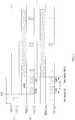
- FIG. 2is a schematic block diagram of a video switch according to an embodiment of the present invention
- FIG. 3schematically illustrates an input port switching scheme according to an embodiment of the present invention
- the video switch 1has a first input port P1, a second input port P2, a first switch unit S1, a second switch unit S2, a microcontroller unit 11, and an output port 2.
- the first input port P1includes a first Transition Minimized Differential Signaling (TMDS) transmission channel T1 for transmitting a first TMDS signal TMDS(1) and a first Inter-Integrated Circuit (I2C) channel I1 for transmitting a first I2C signal I2C(1).
- TMDSTransition Minimized Differential Signaling
- I2CInter-Integrated Circuit
- the second input port P2includes a second TMDS transmission channel T2 for transmitting a second TMDS signal TMDS(2) and a second I2C channel 12 for transmitting a second I2C signal I2C(2). Although only two input ports P1 and P2 are shown in this embodiment, more input ports may be provided.
- the first switch unit S1is coupled to the first I2C channel I1 and the second I2C channel 12; it can be selectively switched to the first I2C channel I1 to output the first I2C signal I2C(1) to the output port 2.
- the second switch unit S2is coupled to the first TMDS transmission channel T1 and the second TMDS transmission channel T2; it can be selectively switched to the first TMDS transmission channel T1 to output the first TMDS signal TMDS(1) to the output port 2. As shown in FIG. 3 , at this time the output port 2 outputs the video image of the first input port P1.
- the Hot Plug Detection (HPD) pin of the second port P2is first pulled to a high voltage level from a low voltage level, and the first switch unit S1 switches from the first I2C channel I1 to the second I2C channel 12.
- HPDHot Plug Detection
- the processbegins to read the Extended Display Identification Data (EDID) from the second input port P2 and to perform High-Bandwidth Digital Content Protection (HDCP) authentication (i.e. the first authentication).
- EDIDExtended Display Identification Data
- HDCPHigh-Bandwidth Digital Content Protection
- this time periodis defined as a specific time period; i.e., this specific time period is the time period for reading the EDID (TEDID) and the time period for performing HDCP first authentication (Tauth1). It should be noted that, within this specific time period, the second switch unit S2 will output the first TMDS signal TMDS(1) so as to maintain the output video image of the first port P1.
- the microcontroller unit 11which is coupled to the first switch unit S1 and the second switch unit S2, monitors and learns about this specific time period; and only after the specific time period has passed, the second switch unit S2 outputs the second TMDS signal TMDS(2) to the output port 2.
- an imitation load circuit 13coupled to the second TMDS transmission channel T2 needs to the made conductive, so that the second input port P2 deems the output port 2 to be present and will start the EDID reading and the HDCP authentication (first authentication) process by the second input port P2.
- the imitation load circuit 13may be a simple switching circuit, but is not limited to such.
- each TMDS transmission channelhas an imitation load circuit coupled to it, but in alternative embodiments, one imitation load circuit may be provided and coupled to all of the TMDS transmission channels; a simple control circuit may be used to respectively make it conductive with one of the TMDS transmission channel as needed.
- the output TMDS signal TMDS(out)can remain uninterrupted.
- the blank screen produced during the EDID reading time period and HDCP authentication time period (i.e. TEDID and Tauth1) in conventional technologyis replaced in this embodiment, by using the above switching method, with the video image of the first input port.
- the blank screenis replaced; moreover, by using the asynchronous switching technique, i.e. to switch the I2C signal first and then switch the TMDS signal, the video image switching time can be reduced to approximately 0.3 to 1 second.
- the microcontroller unitmonitors and learns the duration of the EDID reading time period (TEDID) and HDCP authentication time period (Tauth1), and uses these time durations as the basis for switching the video images next time. It should be noted that the embodiments of the present invention are applicable to switching images of the same resolution.
- An embodiment of the present inventionalso provides a video switching method, as shown in FIG. 4 , which includes the following steps: (A1) providing a video switch, which includes a first input port, for transmitting a first TMDS signal and a first I2C signal, and a second input port, for transmitting a second TMDS signal and a second I2C signal; (A2) the video switch selecting the first input port to output the first TMDS signal and the first I2C signal; (A3) the video switch switching from the first input port to the second input port; and (A4) when switching from the first input port to the second input port, the video switch first outputting the second I2C signal for a specified period of time, and then outputting the second TMDS signal.
- Another embodiment of the present inventionprovides a video switching method, which includes the following steps: (B1) providing a video switch, which includes a first input port for receiving a first video signal from a first video source which contains a first TMDS signal, a second input port for receiving a second video signal from a second video source which contains a second TMDS signal, and an output port coupled to a display device for receiving the first or second video signal; (B2) the video switch selecting the first input port to output the first video signal; (B3) the video switch switching from the first input port to the second input port; and (B4) when switching from the first input port to the second input port, the video switch causing the second video source and the display device to perform I2C communication for a specified period of time, and then outputting the second TMDS signal to the display device.
- the first input port P1can receive the first video signal (not shown in the drawings) from the coupled first video source (not shown in the drawings), and the first video signal can include a first TMDS signal;
- the second input port P2can receive the second video signal (not shown in the drawings) from the coupled second video source (not shown in the drawings), and the second video signal can include a second TMDS signal;
- the output port 2can be coupled to the display device which can receive and display the first or second video signal.
- the switching method and effectare similar to the earlier-described embodiment and are not repeated here.
- the video switch and related switching methodhave the following advantages: By using simple hardware and asynchronous switching of I2C and TMDS signals, image-out time can be improved with relatively low cost, and the blank screen during video switching is prevented. In other words, it can use a transition image to replace the blank screen, and the asynchronous switching can reduce the switching time to less than 1 second.
Landscapes
- Engineering & Computer Science (AREA)
- Multimedia (AREA)
- Signal Processing (AREA)
- Physics & Mathematics (AREA)
- Computer Hardware Design (AREA)
- General Physics & Mathematics (AREA)
- Theoretical Computer Science (AREA)
- Computer Networks & Wireless Communication (AREA)
- Two-Way Televisions, Distribution Of Moving Picture Or The Like (AREA)
- Studio Circuits (AREA)
- Controls And Circuits For Display Device (AREA)
- Closed-Circuit Television Systems (AREA)
Description
- This invention relates to a video switch and related switching method, and in particular, it relates to an asynchronous video switch and related switching method.
- In recent years, HDMI interface, which is a digital transmission interface more efficient and faster than the DVI interface, has been developed. More and more digital audio and video equipment (such as playback device, display device, etc.) are now adopting this interface. Also, a High-Bandwidth Digital Content Protection (HDCP) standard is developed in recent years to protect copyright of digital audio and video content and prevent illegal duplication or spreading of such content during transmission or playing. The HDCP standard includes an authentication protocol; using such a protocol, the HDCP transmitting device (such as a playback device) can confirm whether a particular HDCP receiving device (e.g. a display device) is authorized to receive content protected by HDCP. When access right is confirmed, the content protected by HDCP security protection can be transmitted from the HDCP transmitting device to the HDCP receiving device using a shared secret key which is established during the authentication process, to prevent illegal capture of HDCP protected content by an illegitimate device.
- However, as shown in
FIG. 1 , when the display device switches to a different image, for lower end televisions, the time required from reading the Extended Display Identification Data (EDID) and confirming the HDCP authentication data (i.e. the first authentication, "auth-1") to outputting the image is approximately 4 seconds. For higher end televisions, this time is approximately 1 to 2 seconds. Moreover, when switching images, the display screen is blank (i.e. no image is shown). These cause long delays and undesirable visual effect for the viewer. US 2010/0177892 A1 discloses a method, apparatus and system for providing pre-authentication and keep-authentication of content protected ports system employing a ratio of one decipher processing engine associated with multiple ports.US 2011/0022739 A1 discloses a high-definition multimedia interface (HDMI) switch configured to receive notification of a switch from a current HDMI source to a new HDMI source to enable switching between HDMI sources with a reduced delay.US 2012/0027203 A1 discloses a decoder extracting a synchronization signal from a data stream received via an active port.US 2010/0315553 A1 discloses an audio-video data synchronization method whereby an increase in the amount of control message transmission can be suppressed and the video output can be prevented from being interrupted.- Accordingly, an object of the present invention is to provide a video switch, which includes: a first input port, including a first Transition Minimized Differential Signaling (TMDS) transmission channel for transmitting a first TMDS signal and a first Inter-Integrated Circuit (I2C) channel for transmitting a first I2C signal; a second input port, including a second TMDS transmission channel for transmitting a second TMDS signal and a second I2C channel for transmitting a second I2C signal; a first switch unit, coupled to the first I2C channel and the
second I2C channel 12, and a second switch unit, coupled to the first TMDS transmission channel and the second TMDS transmission channel, the video switching function being performed as defined in the appendedindependent claim 1. - In another aspect, this invention provides a video switching method as defined in the appended independent claim 5.
- Advantageous embodiments are defined in the appended dependent claims.
- Compared to conventional technologies, the video switch according to embodiments of the present invention use simple hardware and asynchronous switching of I2C and TMDS to achieve faster image out time with low cost, and can prevent the problem of blank screen during switching.
FIG. 1 schematically illustrates a conventional input port switching scheme.FIG. 2 is a schematic block diagram of a video switch according to an embodiment of the present invention.FIG. 3 schematically illustrates an input port switching scheme according to an embodiment of the present invention.FIG. 4 schematically illustrates a video switching method according to an embodiment of the present invention.FIG. 5 schematically illustrates a video switching method according to another embodiment of the present invention.- Embodiments of the present invention are described below with reference to the drawings. While the embodiments are described in specific details, it should be understood that these specific details do not limit the scope of the present invention. Also, to avoid overcrowding in the drawings, some commonly known structural elements are shown schematically in the drawings.
- Refer to
FIG. 2 andFIG. 3 .FIG. 2 is a schematic block diagram of a video switch according to an embodiment of the present invention, andFIG. 3 schematically illustrates an input port switching scheme according to an embodiment of the present invention. Thevideo switch 1 has a first input port P1, a second input port P2, a first switch unit S1, a second switch unit S2, a microcontroller unit 11, and anoutput port 2. The first input port P1 includes a first Transition Minimized Differential Signaling (TMDS) transmission channel T1 for transmitting a first TMDS signal TMDS(1) and a first Inter-Integrated Circuit (I2C) channel I1 for transmitting a first I2C signal I2C(1). The second input port P2 includes a second TMDS transmission channel T2 for transmitting a second TMDS signal TMDS(2) and asecond I2C channel 12 for transmitting a second I2C signal I2C(2). Although only two input ports P1 and P2 are shown in this embodiment, more input ports may be provided. - The first switch unit S1 is coupled to the first I2C channel I1 and the
second I2C channel 12; it can be selectively switched to the first I2C channel I1 to output the first I2C signal I2C(1) to theoutput port 2. The second switch unit S2 is coupled to the first TMDS transmission channel T1 and the second TMDS transmission channel T2; it can be selectively switched to the first TMDS transmission channel T1 to output the first TMDS signal TMDS(1) to theoutput port 2. As shown inFIG. 3 , at this time theoutput port 2 outputs the video image of the first input port P1. - At this time, if the video image is to be switched from the first input port P1 to the second input port P2, the Hot Plug Detection (HPD) pin of the second port P2 is first pulled to a high voltage level from a low voltage level, and the first switch unit S1 switches from the first I2C channel I1 to the
second I2C channel 12. Continue to refer toFIG. 3 , at this time, the process begins to read the Extended Display Identification Data (EDID) from the second input port P2 and to perform High-Bandwidth Digital Content Protection (HDCP) authentication (i.e. the first authentication). In this embodiment, this time period is defined as a specific time period; i.e., this specific time period is the time period for reading the EDID (TEDID) and the time period for performing HDCP first authentication (Tauth1). It should be noted that, within this specific time period, the second switch unit S2 will output the first TMDS signal TMDS(1) so as to maintain the output video image of the first port P1. - The microcontroller unit 11, which is coupled to the first switch unit S1 and the second switch unit S2, monitors and learns about this specific time period; and only after the specific time period has passed, the second switch unit S2 outputs the second TMDS signal TMDS(2) to the
output port 2. It should be noted that before the second switch unit S2 outputs the second TMDS signal TMDS(2), animitation load circuit 13 coupled to the second TMDS transmission channel T2 needs to the made conductive, so that the second input port P2 deems theoutput port 2 to be present and will start the EDID reading and the HDCP authentication (first authentication) process by the second input port P2. In this embodiment, theimitation load circuit 13 may be a simple switching circuit, but is not limited to such. Also, in the illustrated embodiment, each TMDS transmission channel has an imitation load circuit coupled to it, but in alternative embodiments, one imitation load circuit may be provided and coupled to all of the TMDS transmission channels; a simple control circuit may be used to respectively make it conductive with one of the TMDS transmission channel as needed. - As seem from the lower part of
FIG. 3 , by using the above asynchronous switching technique, the output TMDS signal TMDS(out) can remain uninterrupted. The blank screen produced during the EDID reading time period and HDCP authentication time period (i.e. TEDID and Tauth1) in conventional technology is replaced in this embodiment, by using the above switching method, with the video image of the first input port. In short, by using such a transition image, the blank screen is replaced; moreover, by using the asynchronous switching technique, i.e. to switch the I2C signal first and then switch the TMDS signal, the video image switching time can be reduced to approximately 0.3 to 1 second. - In this embodiment, each time the input port is switched, the microcontroller unit monitors and learns the duration of the EDID reading time period (TEDID) and HDCP authentication time period (Tauth1), and uses these time durations as the basis for switching the video images next time. It should be noted that the embodiments of the present invention are applicable to switching images of the same resolution.
- An embodiment of the present invention also provides a video switching method, as shown in
FIG. 4 , which includes the following steps: (A1) providing a video switch, which includes a first input port, for transmitting a first TMDS signal and a first I2C signal, and a second input port, for transmitting a second TMDS signal and a second I2C signal; (A2) the video switch selecting the first input port to output the first TMDS signal and the first I2C signal; (A3) the video switch switching from the first input port to the second input port; and (A4) when switching from the first input port to the second input port, the video switch first outputting the second I2C signal for a specified period of time, and then outputting the second TMDS signal. - The hardware structure and the detailed switching method are described in the embodiments above and not repeated here.
- Another embodiment of the present invention provides a video switching method, which includes the following steps: (B1) providing a video switch, which includes a first input port for receiving a first video signal from a first video source which contains a first TMDS signal, a second input port for receiving a second video signal from a second video source which contains a second TMDS signal, and an output port coupled to a display device for receiving the first or second video signal; (B2) the video switch selecting the first input port to output the first video signal; (B3) the video switch switching from the first input port to the second input port; and (B4) when switching from the first input port to the second input port, the video switch causing the second video source and the display device to perform I2C communication for a specified period of time, and then outputting the second TMDS signal to the display device.
- Differences between tis embodiment and the earlier-described embodiment include that, the first input port P1 can receive the first video signal (not shown in the drawings) from the coupled first video source (not shown in the drawings), and the first video signal can include a first TMDS signal; the second input port P2 can receive the second video signal (not shown in the drawings) from the coupled second video source (not shown in the drawings), and the second video signal can include a second TMDS signal; the
output port 2 can be coupled to the display device which can receive and display the first or second video signal. The switching method and effect are similar to the earlier-described embodiment and are not repeated here. - Compared to conventional technologies, the video switch and related switching method according to embodiments of the present invention have the following advantages: By using simple hardware and asynchronous switching of I2C and TMDS signals, image-out time can be improved with relatively low cost, and the blank screen during video switching is prevented. In other words, it can use a transition image to replace the blank screen, and the asynchronous switching can reduce the switching time to less than 1 second.
- Descriptions of the preferred embodiments are given above to illustrate the principle and features of the present invention, and do not limit the scope of the invention. To the contrary, it is intended that the present invention cover modifications and variations that come within the scope of the appended claims.
- The scope of the invention should be interpreted broadly based on the appended claims.
Claims (8)
- A video switch (1), comprising:a first input port (P1);a first Transition Minimized Differential Signaling (TMDS) transmission channel (T1) coupled to the first input port (P1) and configured to transmit a first TMDS signal;a first Inter-Integrated Circuit (I2C) channel (I1) coupled to the first input port (P1) and configured to transmit a first I2C signal;a second input port (P2);a second TMDS transmission channel (T2) coupled to the second input port (P2) and configured to transmit a second TMDS signal;a second I2C channel (12) coupled to the second input port (P2) and configured to transmit a second I2C signal;a first switch unit (S1), selectively coupled to the first I2C channel (I1) and the second I2C channel (12), when the first switch unit (S1) is coupled to the first I2C channel (I1), the first switch unit (S1) receiving the first I2C signal from the first I2C channel (I1) and outputting the first I2C signal;a second switch unit (S2), selectively coupled to the first TMDS transmission channel (T1) and the second TMDS transmission channel (T2), when the second switch unit (S2) is coupled to the first TMDS transmission channel (T1), the second switch unit (S2) receiving the first TMDS signal from the first TMDS transmission channel (T1) and outputting the first TMDS signal;a microcontroller unit (11) coupled to the first switch unit (S1) and the second switch unit (S2); andan output port (2) coupled to the first switch unit (S1) and the second switch unit (S2);wherein when switching from the first input port (P1) to the second input port (P2):the first switch unit (S1) is coupled to the second I2C channel (I2) and outputs the second I2C signal to the output port (2), and after the first switch unit (S1) outputs the second I2C signal to the output port (2) for a specified time period, the second switch unit (S2) starts to outputs the second TMDS signal to the output port (2);characterized in thatthe specified time period includes a time period for reading Extended Display Identification Data (EDID) and a time period for performing High-Bandwidth Digital Content Protection (HDCP) first authentication, and the specified time period is determined by the microcontroller unit (11) monitoring the time period for reading the EDID and the time period for performing the HDCP first authentication; during the specified time period, the second switch unit (S2) outputs the first TMDS signal to the output port (2).
- The video switch of claim 1,characterized in that the video switch (1) further comprises an imitation load circuit (13), for providing an imitation load signal to be output by the second input port (P2) before the second switch unit (S2) outputs the second TMDS signal.
- The video switch of claim 1,characterized in that after a Hot Plug Detection (HPD) pin of the second input port (P2) is pulled from a low voltage level to a high voltage level, the first switch unit (S1) originally coupled to the first I2C channel (I1) is switched to be coupled to the second I2C channel (12).
- The video switch of claim 1,characterized in that a resolution of the first TMDS signal is equal to a resolution of the second TMDS signal.
- A video switching method, comprising:providing a video switch comprising a first input port (P1), a first TransitionMinimized Differential Signaling (TMDS) transmission channel, a first Inter-Integrated Circuit (I2C) channel, a second input port (P2), a second TMDS transmission channel, a second I2C channel, a first switch unit, a second switch unit, a microcontroller unit and an output port, which the first TMDS transmission channel is coupled to the first input port and configured to transmit a first TMDS signal; the first I2C channel is coupled to the first input port and configured to transmit a first I2C signal; the second TMDS transmission channel is coupled to the second input port and configured to transmit a second TMDS signal; the second I2C channel is coupled to the second input port and configured to transmit a second I2C signal; the first switch unit is selectively coupled to the first I2C channel and the second I2C channel; the second switch unit is selectively coupled to the first TMDS transmission channel and the second TMDS transmission channel; the microcontroller unit is coupled to the first switch unit and the second switch unit; the output port is coupled to the first switch unit and the second switch unit;when the first switch unit is coupled to the first I2C channel and the second switch unit is coupled to the first TMDS transmission channel, the first switch unit receiving the first I2C signal from the first I2C channel andoutputting the first I2C signal to the output port and the second switch unit receiving the first TMDS signal from the first TMDS transmission channel and outputting the first TMDS signal to the output port;wherein when switching from the first input port (P1) to the second input port (P2):the first switch unit is coupled to the second I2C channel, the first switch unit outputting the second I2C signal to the output port; andafter the first switch unit outputs the second I2C signal to the output port for a specified time period, the second switch unit starting to outputs the second TMDS signal to the output port;characterized in thatthe specified time period includes a time period for reading Extended Display Identification Data (EDID) and a time period for performing High-Bandwidth Digital Content Protection (HDCP) first authentication, and the specified time period is determined by the microcontroller unit monitoring the time period for reading the EDID and the time period for performing the HDCP first authentication; during the specified time period, the second switch unit outputs the first TMDS signal to the output port.
- The video switching method of claim 5,characterized in that the video switching method further comprises:
providing an imitation load circuit, for outputting an imitation load signal to be output by the second input port before the video switch outputs the second TMDS signal. - The video switching method of claim 5,characterized in that a resolution of the first TMDS signal is equal to a resolution of the second TMDS signal.
- The video switching method of claim 5,characterized in that after a Hot Plug Detection (HPD) pin of the second input port is pulled to a high voltage level, the first switch unit originally coupled to the first I2C channel is switched to be coupled to the second I2C channel.
Applications Claiming Priority (1)
| Application Number | Priority Date | Filing Date | Title |
|---|---|---|---|
| TW104102743ATWI554113B (en) | 2015-01-27 | 2015-01-27 | Video switch and switching method thereof |
Publications (2)
| Publication Number | Publication Date |
|---|---|
| EP3051801A1 EP3051801A1 (en) | 2016-08-03 |
| EP3051801B1true EP3051801B1 (en) | 2020-01-08 |
Family
ID=54782444
Family Applications (1)
| Application Number | Title | Priority Date | Filing Date |
|---|---|---|---|
| EP15196203.2AActiveEP3051801B1 (en) | 2015-01-27 | 2015-11-25 | Video switch and switching method thereof |
Country Status (4)
| Country | Link |
|---|---|
| US (1) | US9413986B1 (en) |
| EP (1) | EP3051801B1 (en) |
| CN (1) | CN106210564B (en) |
| TW (1) | TWI554113B (en) |
Families Citing this family (12)
| Publication number | Priority date | Publication date | Assignee | Title |
|---|---|---|---|---|
| TWI611697B (en)* | 2016-10-04 | 2018-01-11 | 神雲科技股份有限公司 | Hdmi device and method for controlling the same |
| TWI626851B (en)* | 2017-03-14 | 2018-06-11 | 宏正自動科技股份有限公司 | Video switching apparatus, video switching system, and video switching method |
| US10430358B2 (en) | 2017-03-30 | 2019-10-01 | Mitac Computing Technology Corporation | High-definition multimedia interface apparatus capable of communication with slave/master apparatus utilizing the same HDMI port and method for controlling the same |
| TWI653889B (en) | 2017-09-12 | 2019-03-11 | 宏正自動科技股份有限公司 | Video signal transmission switching apparatus |
| TWI675591B (en)* | 2017-12-07 | 2019-10-21 | 宏正自動科技股份有限公司 | Video streaming synchronization switching method for video wall system |
| CN109829345B (en)* | 2018-12-27 | 2022-03-08 | 苏州佳世达电通有限公司 | Method for reducing time required for scanning multiple transmission ports and scanning system |
| CN111770294B (en)* | 2019-03-29 | 2022-10-28 | 瑞昱半导体股份有限公司 | Receiving circuit and signal processing method for high-resolution multimedia interface |
| CN110248115B (en)* | 2019-06-21 | 2020-11-24 | 上海摩象网络科技有限公司 | Image processing method, device and storage medium |
| TWI768439B (en)* | 2020-08-20 | 2022-06-21 | 黃湘豪 | Non-intruder inspecting and injecting protocol device |
| CN112565633B (en)* | 2020-12-08 | 2022-10-21 | 威创集团股份有限公司 | Detection system and video receiving box thereof |
| TWI859944B (en)* | 2023-06-21 | 2024-10-21 | 宏正自動科技股份有限公司 | Method of generating image signal and display system |
| CN117676060B (en)* | 2024-02-01 | 2024-06-11 | 深圳市灰度科技有限公司 | Video signal transmission circuit and system |
Family Cites Families (12)
| Publication number | Priority date | Publication date | Assignee | Title |
|---|---|---|---|---|
| JP2005051558A (en)* | 2003-07-29 | 2005-02-24 | Matsushita Electric Ind Co Ltd | Transmission device, reception device, and transmission / reception system |
| JP5029121B2 (en)* | 2007-04-25 | 2012-09-19 | ソニー株式会社 | Data receiving apparatus, data transmitting apparatus, information processing method, and computer program |
| TWI419006B (en) | 2007-09-21 | 2013-12-11 | Mstar Semiconductor Inc | Fast switching method and related device |
| US8238726B2 (en) | 2008-02-06 | 2012-08-07 | Panasonic Corporation | Audio-video data synchronization method, video output device, audio output device, and audio-video output system |
| CN101282444B (en)* | 2008-03-18 | 2011-06-15 | 青岛海信电器股份有限公司 | Receiving switching mechanism, TV set containing the same |
| JP5210244B2 (en) | 2008-08-13 | 2013-06-12 | キヤノン株式会社 | Video control apparatus and control method for controlling video control apparatus |
| US8374346B2 (en)* | 2009-01-09 | 2013-02-12 | Silicon Image, Inc. | Method, apparatus, and system for pre-authentication and keep-authentication of content protected ports |
| EP2280542A1 (en)* | 2009-07-21 | 2011-02-02 | Nxp B.V. | Fast HDMI switching with conditional reset mechanism |
| US8832844B2 (en) | 2009-12-04 | 2014-09-09 | Parade Technologies, Ltd. | Fast switching for multimedia interface system having content protection |
| JP2012029214A (en) | 2010-07-27 | 2012-02-09 | Rohm Co Ltd | Interface circuit and electronic device using the same |
| US8713316B2 (en)* | 2011-12-13 | 2014-04-29 | Crestron Electronics Inc. | System, apparatus and method for enabling/disabling display data channel access to enable/disable high-bandwidth digital content protection |
| CN103618915A (en)* | 2013-11-13 | 2014-03-05 | 深圳市同洲电子股份有限公司 | Multi-screen interaction method and device |
- 2015
- 2015-01-27TWTW104102743Apatent/TWI554113B/enactive
- 2015-06-02CNCN201510294046.3Apatent/CN106210564B/enactiveActive
- 2015-10-26USUS14/922,511patent/US9413986B1/enactiveActive
- 2015-11-25EPEP15196203.2Apatent/EP3051801B1/enactiveActive
Non-Patent Citations (1)
| Title |
|---|
| None* |
Also Published As
| Publication number | Publication date |
|---|---|
| TW201628401A (en) | 2016-08-01 |
| US20160219226A1 (en) | 2016-07-28 |
| TWI554113B (en) | 2016-10-11 |
| EP3051801A1 (en) | 2016-08-03 |
| CN106210564A (en) | 2016-12-07 |
| CN106210564B (en) | 2019-05-21 |
| US9413986B1 (en) | 2016-08-09 |
Similar Documents
| Publication | Publication Date | Title |
|---|---|---|
| EP3051801B1 (en) | Video switch and switching method thereof | |
| EP2274907B1 (en) | Method and system for deciphering media content stream | |
| KR101724484B1 (en) | Method, apparatus, and system for simultaneously previewing contents from multiple protected sources | |
| JP5797267B2 (en) | Mechanism for partial encryption of data stream | |
| US11716189B2 (en) | Interface circuit and information processing system | |
| US8331561B2 (en) | Fast switching between digital video sources | |
| US20110134330A1 (en) | Fast switching for multimedia interface system having content protection | |
| US8174619B2 (en) | Reception apparatus and method of controlling image output by reception apparatus | |
| KR101538711B1 (en) | Detection of encryption utilizing error detection for received data | |
| KR20170028165A (en) | Image processing apparatus and control method thereof | |
| US8242940B2 (en) | Transitioning digital data processors between power savings and non-power savings modes | |
| US8316391B2 (en) | Video signal processing apparatus and set top box | |
| WO2010070812A1 (en) | Data transmission circuit | |
| US20180220185A1 (en) | Device and method for modifying a stream of encrypted multimedia data |
Legal Events
| Date | Code | Title | Description |
|---|---|---|---|
| PUAI | Public reference made under article 153(3) epc to a published international application that has entered the european phase | Free format text:ORIGINAL CODE: 0009012 | |
| AK | Designated contracting states | Kind code of ref document:A1 Designated state(s):AL AT BE BG CH CY CZ DE DK EE ES FI FR GB GR HR HU IE IS IT LI LT LU LV MC MK MT NL NO PL PT RO RS SE SI SK SM TR | |
| AX | Request for extension of the european patent | Extension state:BA ME | |
| STAA | Information on the status of an ep patent application or granted ep patent | Free format text:STATUS: REQUEST FOR EXAMINATION WAS MADE | |
| 17P | Request for examination filed | Effective date:20170202 | |
| RBV | Designated contracting states (corrected) | Designated state(s):AL AT BE BG CH CY CZ DE DK EE ES FI FR GB GR HR HU IE IS IT LI LT LU LV MC MK MT NL NO PL PT RO RS SE SI SK SM TR | |
| REG | Reference to a national code | Ref country code:DE Ref legal event code:R079 Ref document number:602015045072 Country of ref document:DE Free format text:PREVIOUS MAIN CLASS: H04N0005765000 Ipc:G09G0005000000 | |
| RIC1 | Information provided on ipc code assigned before grant | Ipc:G09G 5/00 20060101AFI20190531BHEP Ipc:H04N 21/4363 20110101ALI20190531BHEP | |
| GRAP | Despatch of communication of intention to grant a patent | Free format text:ORIGINAL CODE: EPIDOSNIGR1 | |
| STAA | Information on the status of an ep patent application or granted ep patent | Free format text:STATUS: GRANT OF PATENT IS INTENDED | |
| INTG | Intention to grant announced | Effective date:20190712 | |
| GRAS | Grant fee paid | Free format text:ORIGINAL CODE: EPIDOSNIGR3 | |
| GRAA | (expected) grant | Free format text:ORIGINAL CODE: 0009210 | |
| STAA | Information on the status of an ep patent application or granted ep patent | Free format text:STATUS: THE PATENT HAS BEEN GRANTED | |
| AK | Designated contracting states | Kind code of ref document:B1 Designated state(s):AL AT BE BG CH CY CZ DE DK EE ES FI FR GB GR HR HU IE IS IT LI LT LU LV MC MK MT NL NO PL PT RO RS SE SI SK SM TR | |
| REG | Reference to a national code | Ref country code:GB Ref legal event code:FG4D | |
| REG | Reference to a national code | Ref country code:CH Ref legal event code:EP | |
| REG | Reference to a national code | Ref country code:DE Ref legal event code:R096 Ref document number:602015045072 Country of ref document:DE | |
| REG | Reference to a national code | Ref country code:IE Ref legal event code:FG4D | |
| REG | Reference to a national code | Ref country code:AT Ref legal event code:REF Ref document number:1223670 Country of ref document:AT Kind code of ref document:T Effective date:20200215 | |
| REG | Reference to a national code | Ref country code:NL Ref legal event code:MP Effective date:20200108 | |
| REG | Reference to a national code | Ref country code:LT Ref legal event code:MG4D | |
| PG25 | Lapsed in a contracting state [announced via postgrant information from national office to epo] | Ref country code:PT Free format text:LAPSE BECAUSE OF FAILURE TO SUBMIT A TRANSLATION OF THE DESCRIPTION OR TO PAY THE FEE WITHIN THE PRESCRIBED TIME-LIMIT Effective date:20200531 Ref country code:NL Free format text:LAPSE BECAUSE OF FAILURE TO SUBMIT A TRANSLATION OF THE DESCRIPTION OR TO PAY THE FEE WITHIN THE PRESCRIBED TIME-LIMIT Effective date:20200108 Ref country code:LT Free format text:LAPSE BECAUSE OF FAILURE TO SUBMIT A TRANSLATION OF THE DESCRIPTION OR TO PAY THE FEE WITHIN THE PRESCRIBED TIME-LIMIT Effective date:20200108 Ref country code:FI Free format text:LAPSE BECAUSE OF FAILURE TO SUBMIT A TRANSLATION OF THE DESCRIPTION OR TO PAY THE FEE WITHIN THE PRESCRIBED TIME-LIMIT Effective date:20200108 Ref country code:NO Free format text:LAPSE BECAUSE OF FAILURE TO SUBMIT A TRANSLATION OF THE DESCRIPTION OR TO PAY THE FEE WITHIN THE PRESCRIBED TIME-LIMIT Effective date:20200408 Ref country code:RS Free format text:LAPSE BECAUSE OF FAILURE TO SUBMIT A TRANSLATION OF THE DESCRIPTION OR TO PAY THE FEE WITHIN THE PRESCRIBED TIME-LIMIT Effective date:20200108 | |
| PG25 | Lapsed in a contracting state [announced via postgrant information from national office to epo] | Ref country code:IS Free format text:LAPSE BECAUSE OF FAILURE TO SUBMIT A TRANSLATION OF THE DESCRIPTION OR TO PAY THE FEE WITHIN THE PRESCRIBED TIME-LIMIT Effective date:20200508 Ref country code:HR Free format text:LAPSE BECAUSE OF FAILURE TO SUBMIT A TRANSLATION OF THE DESCRIPTION OR TO PAY THE FEE WITHIN THE PRESCRIBED TIME-LIMIT Effective date:20200108 Ref country code:GR Free format text:LAPSE BECAUSE OF FAILURE TO SUBMIT A TRANSLATION OF THE DESCRIPTION OR TO PAY THE FEE WITHIN THE PRESCRIBED TIME-LIMIT Effective date:20200409 Ref country code:SE Free format text:LAPSE BECAUSE OF FAILURE TO SUBMIT A TRANSLATION OF THE DESCRIPTION OR TO PAY THE FEE WITHIN THE PRESCRIBED TIME-LIMIT Effective date:20200108 Ref country code:LV Free format text:LAPSE BECAUSE OF FAILURE TO SUBMIT A TRANSLATION OF THE DESCRIPTION OR TO PAY THE FEE WITHIN THE PRESCRIBED TIME-LIMIT Effective date:20200108 Ref country code:BG Free format text:LAPSE BECAUSE OF FAILURE TO SUBMIT A TRANSLATION OF THE DESCRIPTION OR TO PAY THE FEE WITHIN THE PRESCRIBED TIME-LIMIT Effective date:20200408 | |
| REG | Reference to a national code | Ref country code:DE Ref legal event code:R097 Ref document number:602015045072 Country of ref document:DE | |
| PG25 | Lapsed in a contracting state [announced via postgrant information from national office to epo] | Ref country code:EE Free format text:LAPSE BECAUSE OF FAILURE TO SUBMIT A TRANSLATION OF THE DESCRIPTION OR TO PAY THE FEE WITHIN THE PRESCRIBED TIME-LIMIT Effective date:20200108 Ref country code:SM Free format text:LAPSE BECAUSE OF FAILURE TO SUBMIT A TRANSLATION OF THE DESCRIPTION OR TO PAY THE FEE WITHIN THE PRESCRIBED TIME-LIMIT Effective date:20200108 Ref country code:DK Free format text:LAPSE BECAUSE OF FAILURE TO SUBMIT A TRANSLATION OF THE DESCRIPTION OR TO PAY THE FEE WITHIN THE PRESCRIBED TIME-LIMIT Effective date:20200108 Ref country code:ES Free format text:LAPSE BECAUSE OF FAILURE TO SUBMIT A TRANSLATION OF THE DESCRIPTION OR TO PAY THE FEE WITHIN THE PRESCRIBED TIME-LIMIT Effective date:20200108 Ref country code:RO Free format text:LAPSE BECAUSE OF FAILURE TO SUBMIT A TRANSLATION OF THE DESCRIPTION OR TO PAY THE FEE WITHIN THE PRESCRIBED TIME-LIMIT Effective date:20200108 Ref country code:CZ Free format text:LAPSE BECAUSE OF FAILURE TO SUBMIT A TRANSLATION OF THE DESCRIPTION OR TO PAY THE FEE WITHIN THE PRESCRIBED TIME-LIMIT Effective date:20200108 Ref country code:SK Free format text:LAPSE BECAUSE OF FAILURE TO SUBMIT A TRANSLATION OF THE DESCRIPTION OR TO PAY THE FEE WITHIN THE PRESCRIBED TIME-LIMIT Effective date:20200108 | |
| PLBE | No opposition filed within time limit | Free format text:ORIGINAL CODE: 0009261 | |
| STAA | Information on the status of an ep patent application or granted ep patent | Free format text:STATUS: NO OPPOSITION FILED WITHIN TIME LIMIT | |
| REG | Reference to a national code | Ref country code:AT Ref legal event code:MK05 Ref document number:1223670 Country of ref document:AT Kind code of ref document:T Effective date:20200108 | |
| 26N | No opposition filed | Effective date:20201009 | |
| PG25 | Lapsed in a contracting state [announced via postgrant information from national office to epo] | Ref country code:IT Free format text:LAPSE BECAUSE OF FAILURE TO SUBMIT A TRANSLATION OF THE DESCRIPTION OR TO PAY THE FEE WITHIN THE PRESCRIBED TIME-LIMIT Effective date:20200108 Ref country code:AT Free format text:LAPSE BECAUSE OF FAILURE TO SUBMIT A TRANSLATION OF THE DESCRIPTION OR TO PAY THE FEE WITHIN THE PRESCRIBED TIME-LIMIT Effective date:20200108 | |
| PG25 | Lapsed in a contracting state [announced via postgrant information from national office to epo] | Ref country code:PL Free format text:LAPSE BECAUSE OF FAILURE TO SUBMIT A TRANSLATION OF THE DESCRIPTION OR TO PAY THE FEE WITHIN THE PRESCRIBED TIME-LIMIT Effective date:20200108 Ref country code:SI Free format text:LAPSE BECAUSE OF FAILURE TO SUBMIT A TRANSLATION OF THE DESCRIPTION OR TO PAY THE FEE WITHIN THE PRESCRIBED TIME-LIMIT Effective date:20200108 | |
| PG25 | Lapsed in a contracting state [announced via postgrant information from national office to epo] | Ref country code:MC Free format text:LAPSE BECAUSE OF FAILURE TO SUBMIT A TRANSLATION OF THE DESCRIPTION OR TO PAY THE FEE WITHIN THE PRESCRIBED TIME-LIMIT Effective date:20200108 | |
| REG | Reference to a national code | Ref country code:CH Ref legal event code:PL | |
| PG25 | Lapsed in a contracting state [announced via postgrant information from national office to epo] | Ref country code:LU Free format text:LAPSE BECAUSE OF NON-PAYMENT OF DUE FEES Effective date:20201125 | |
| PG25 | Lapsed in a contracting state [announced via postgrant information from national office to epo] | Ref country code:LI Free format text:LAPSE BECAUSE OF NON-PAYMENT OF DUE FEES Effective date:20201130 Ref country code:CH Free format text:LAPSE BECAUSE OF NON-PAYMENT OF DUE FEES Effective date:20201130 | |
| PG25 | Lapsed in a contracting state [announced via postgrant information from national office to epo] | Ref country code:IE Free format text:LAPSE BECAUSE OF NON-PAYMENT OF DUE FEES Effective date:20201125 | |
| PG25 | Lapsed in a contracting state [announced via postgrant information from national office to epo] | Ref country code:TR Free format text:LAPSE BECAUSE OF FAILURE TO SUBMIT A TRANSLATION OF THE DESCRIPTION OR TO PAY THE FEE WITHIN THE PRESCRIBED TIME-LIMIT Effective date:20200108 Ref country code:MT Free format text:LAPSE BECAUSE OF FAILURE TO SUBMIT A TRANSLATION OF THE DESCRIPTION OR TO PAY THE FEE WITHIN THE PRESCRIBED TIME-LIMIT Effective date:20200108 Ref country code:CY Free format text:LAPSE BECAUSE OF FAILURE TO SUBMIT A TRANSLATION OF THE DESCRIPTION OR TO PAY THE FEE WITHIN THE PRESCRIBED TIME-LIMIT Effective date:20200108 | |
| PG25 | Lapsed in a contracting state [announced via postgrant information from national office to epo] | Ref country code:MK Free format text:LAPSE BECAUSE OF FAILURE TO SUBMIT A TRANSLATION OF THE DESCRIPTION OR TO PAY THE FEE WITHIN THE PRESCRIBED TIME-LIMIT Effective date:20200108 Ref country code:AL Free format text:LAPSE BECAUSE OF FAILURE TO SUBMIT A TRANSLATION OF THE DESCRIPTION OR TO PAY THE FEE WITHIN THE PRESCRIBED TIME-LIMIT Effective date:20200108 | |
| PGFP | Annual fee paid to national office [announced via postgrant information from national office to epo] | Ref country code:DE Payment date:20241001 Year of fee payment:10 | |
| PGFP | Annual fee paid to national office [announced via postgrant information from national office to epo] | Ref country code:BE Payment date:20241007 Year of fee payment:10 | |
| PGFP | Annual fee paid to national office [announced via postgrant information from national office to epo] | Ref country code:GB Payment date:20241001 Year of fee payment:10 | |
| PGFP | Annual fee paid to national office [announced via postgrant information from national office to epo] | Ref country code:FR Payment date:20241001 Year of fee payment:10 |