EP3038138A1 - Exposure apparatus, and method of manufacturing devices - Google Patents
Exposure apparatus, and method of manufacturing devicesDownload PDFInfo
- Publication number
- EP3038138A1 EP3038138A1EP15196737.9AEP15196737AEP3038138A1EP 3038138 A1EP3038138 A1EP 3038138A1EP 15196737 AEP15196737 AEP 15196737AEP 3038138 A1EP3038138 A1EP 3038138A1
- Authority
- EP
- European Patent Office
- Prior art keywords
- slider
- mask
- stage
- axis direction
- movable member
- Prior art date
- Legal status (The legal status is an assumption and is not a legal conclusion. Google has not performed a legal analysis and makes no representation as to the accuracy of the status listed.)
- Granted
Links
- 238000004519manufacturing processMethods0.000titleclaimsdescription20
- 230000003287optical effectEffects0.000claimsabstractdescription94
- 238000005286illuminationMethods0.000claimsabstractdescription93
- 238000006243chemical reactionMethods0.000claimsabstractdescription42
- 239000000758substrateSubstances0.000claimsabstractdescription22
- 238000000034methodMethods0.000claimsdescription17
- 238000005339levitationMethods0.000claims4
- 238000003825pressingMethods0.000claims1
- 239000007789gasSubstances0.000description134
- 238000005259measurementMethods0.000description52
- 230000007935neutral effectEffects0.000description41
- 238000010521absorption reactionMethods0.000description34
- 230000002706hydrostatic effectEffects0.000description30
- 230000007246mechanismEffects0.000description28
- 239000001307heliumSubstances0.000description23
- 229910052734heliumInorganic materials0.000description23
- SWQJXJOGLNCZEY-UHFFFAOYSA-Nhelium atomChemical compound[He]SWQJXJOGLNCZEY-UHFFFAOYSA-N0.000description23
- 230000000694effectsEffects0.000description18
- 230000005484gravityEffects0.000description16
- IJGRMHOSHXDMSA-UHFFFAOYSA-NAtomic nitrogenChemical compoundN#NIJGRMHOSHXDMSA-UHFFFAOYSA-N0.000description15
- 238000005192partitionMethods0.000description13
- 238000012546transferMethods0.000description13
- 239000005357flat glassSubstances0.000description10
- 229910052757nitrogenInorganic materials0.000description9
- 229910052756noble gasInorganic materials0.000description9
- 230000008569processEffects0.000description8
- 239000004065semiconductorSubstances0.000description8
- 238000007667floatingMethods0.000description7
- 238000012545processingMethods0.000description7
- 230000002787reinforcementEffects0.000description7
- 238000007789sealingMethods0.000description6
- QVGXLLKOCUKJST-UHFFFAOYSA-Natomic oxygenChemical compound[O]QVGXLLKOCUKJST-UHFFFAOYSA-N0.000description5
- 238000010586diagramMethods0.000description5
- 239000004973liquid crystal related substanceSubstances0.000description5
- 239000001301oxygenSubstances0.000description5
- 229910052760oxygenInorganic materials0.000description5
- 230000003993interactionEffects0.000description4
- 238000002955isolationMethods0.000description4
- 238000005452bendingMethods0.000description3
- 238000007872degassingMethods0.000description3
- 238000013461designMethods0.000description3
- 238000001514detection methodMethods0.000description3
- 238000010894electron beam technologyMethods0.000description3
- 238000005530etchingMethods0.000description3
- 239000011521glassSubstances0.000description3
- 230000010354integrationEffects0.000description3
- 239000000463materialSubstances0.000description3
- QJGQUHMNIGDVPM-UHFFFAOYSA-Nnitrogen groupChemical group[N]QJGQUHMNIGDVPM-UHFFFAOYSA-N0.000description3
- 238000012805post-processingMethods0.000description3
- 238000007781pre-processingMethods0.000description3
- 238000011084recoveryMethods0.000description3
- 230000009467reductionEffects0.000description3
- 238000012360testing methodMethods0.000description3
- XKRFYHLGVUSROY-UHFFFAOYSA-NArgonChemical compound[Ar]XKRFYHLGVUSROY-UHFFFAOYSA-N0.000description2
- RYGMFSIKBFXOCR-UHFFFAOYSA-NCopperChemical compound[Cu]RYGMFSIKBFXOCR-UHFFFAOYSA-N0.000description2
- 229910052691ErbiumInorganic materials0.000description2
- VYPSYNLAJGMNEJ-UHFFFAOYSA-NSilicium dioxideChemical compoundO=[Si]=OVYPSYNLAJGMNEJ-UHFFFAOYSA-N0.000description2
- XUIMIQQOPSSXEZ-UHFFFAOYSA-NSiliconChemical compound[Si]XUIMIQQOPSSXEZ-UHFFFAOYSA-N0.000description2
- 230000015572biosynthetic processEffects0.000description2
- 238000007664blowingMethods0.000description2
- WUKWITHWXAAZEY-UHFFFAOYSA-Lcalcium difluorideChemical compound[F-].[F-].[Ca+2]WUKWITHWXAAZEY-UHFFFAOYSA-L0.000description2
- 229910052802copperInorganic materials0.000description2
- 239000010949copperSubstances0.000description2
- 239000013078crystalSubstances0.000description2
- UYAHIZSMUZPPFV-UHFFFAOYSA-NerbiumChemical compound[Er]UYAHIZSMUZPPFV-UHFFFAOYSA-N0.000description2
- 239000000835fiberSubstances0.000description2
- 239000010436fluoriteSubstances0.000description2
- 230000020169heat generationEffects0.000description2
- 229910052738indiumInorganic materials0.000description2
- APFVFJFRJDLVQX-UHFFFAOYSA-Nindium atomChemical compound[In]APFVFJFRJDLVQX-UHFFFAOYSA-N0.000description2
- 150000002500ionsChemical class0.000description2
- 239000007788liquidSubstances0.000description2
- 239000000696magnetic materialSubstances0.000description2
- QSHDDOUJBYECFT-UHFFFAOYSA-NmercuryChemical compound[Hg]QSHDDOUJBYECFT-UHFFFAOYSA-N0.000description2
- 229910052753mercuryInorganic materials0.000description2
- 229910052751metalInorganic materials0.000description2
- 239000002184metalSubstances0.000description2
- 229910052710siliconInorganic materials0.000description2
- 239000010703siliconSubstances0.000description2
- 239000010409thin filmSubstances0.000description2
- 238000012935AveragingMethods0.000description1
- 239000004215Carbon black (E152)Substances0.000description1
- 238000000018DNA microarrayMethods0.000description1
- KRHYYFGTRYWZRS-UHFFFAOYSA-MFluoride anionChemical compound[F-]KRHYYFGTRYWZRS-UHFFFAOYSA-M0.000description1
- 206010034719Personality changeDiseases0.000description1
- 229910052769YtterbiumInorganic materials0.000description1
- 230000004913activationEffects0.000description1
- 229910052786argonInorganic materials0.000description1
- 239000003795chemical substances by applicationSubstances0.000description1
- 238000012790confirmationMethods0.000description1
- 238000001816coolingMethods0.000description1
- 239000006059cover glassSubstances0.000description1
- 238000005520cutting processMethods0.000description1
- 238000005516engineering processMethods0.000description1
- 238000001900extreme ultraviolet lithographyMethods0.000description1
- 239000010408filmSubstances0.000description1
- 229930195733hydrocarbonNatural products0.000description1
- 150000002430hydrocarbonsChemical class0.000description1
- 238000003384imaging methodMethods0.000description1
- 238000007654immersionMethods0.000description1
- 239000012535impuritySubstances0.000description1
- 239000011261inert gasSubstances0.000description1
- 238000010884ion-beam techniqueMethods0.000description1
- 230000001678irradiating effectEffects0.000description1
- 229910052743kryptonInorganic materials0.000description1
- DNNSSWSSYDEUBZ-UHFFFAOYSA-Nkrypton atomChemical compound[Kr]DNNSSWSSYDEUBZ-UHFFFAOYSA-N0.000description1
- ORUIBWPALBXDOA-UHFFFAOYSA-Lmagnesium fluorideChemical compound[F-].[F-].[Mg+2]ORUIBWPALBXDOA-UHFFFAOYSA-L0.000description1
- 229910001635magnesium fluorideInorganic materials0.000description1
- 230000000873masking effectEffects0.000description1
- -1moistureSubstances0.000description1
- 238000012544monitoring processMethods0.000description1
- 229910052754neonInorganic materials0.000description1
- GKAOGPIIYCISHV-UHFFFAOYSA-Nneon atomChemical compound[Ne]GKAOGPIIYCISHV-UHFFFAOYSA-N0.000description1
- 239000005304optical glassSubstances0.000description1
- 239000005416organic matterSubstances0.000description1
- 230000001151other effectEffects0.000description1
- 230000003647oxidationEffects0.000description1
- 238000007254oxidation reactionMethods0.000description1
- 238000012858packaging processMethods0.000description1
- 239000002245particleSubstances0.000description1
- 230000010399physical interactionEffects0.000description1
- 230000010287polarizationEffects0.000description1
- 238000002360preparation methodMethods0.000description1
- 238000010926purgeMethods0.000description1
- 230000001105regulatory effectEffects0.000description1
- 238000005096rolling processMethods0.000description1
- 239000007787solidSubstances0.000description1
- 238000001179sorption measurementMethods0.000description1
- 238000009834vaporizationMethods0.000description1
- 230000008016vaporizationEffects0.000description1
- NAWDYIZEMPQZHO-UHFFFAOYSA-NytterbiumChemical compound[Yb]NAWDYIZEMPQZHO-UHFFFAOYSA-N0.000description1
Images


Classifications
- G—PHYSICS
- G03—PHOTOGRAPHY; CINEMATOGRAPHY; ANALOGOUS TECHNIQUES USING WAVES OTHER THAN OPTICAL WAVES; ELECTROGRAPHY; HOLOGRAPHY
- G03F—PHOTOMECHANICAL PRODUCTION OF TEXTURED OR PATTERNED SURFACES, e.g. FOR PRINTING, FOR PROCESSING OF SEMICONDUCTOR DEVICES; MATERIALS THEREFOR; ORIGINALS THEREFOR; APPARATUS SPECIALLY ADAPTED THEREFOR
- G03F7/00—Photomechanical, e.g. photolithographic, production of textured or patterned surfaces, e.g. printing surfaces; Materials therefor, e.g. comprising photoresists; Apparatus specially adapted therefor
- G03F7/70—Microphotolithographic exposure; Apparatus therefor
- G03F7/70058—Mask illumination systems
- H—ELECTRICITY
- H01—ELECTRIC ELEMENTS
- H01L—SEMICONDUCTOR DEVICES NOT COVERED BY CLASS H10
- H01L21/00—Processes or apparatus adapted for the manufacture or treatment of semiconductor or solid state devices or of parts thereof
- H01L21/02—Manufacture or treatment of semiconductor devices or of parts thereof
- H01L21/027—Making masks on semiconductor bodies for further photolithographic processing not provided for in group H01L21/18 or H01L21/34
- H01L21/0271—Making masks on semiconductor bodies for further photolithographic processing not provided for in group H01L21/18 or H01L21/34 comprising organic layers
- H01L21/0273—Making masks on semiconductor bodies for further photolithographic processing not provided for in group H01L21/18 or H01L21/34 comprising organic layers characterised by the treatment of photoresist layers
- H01L21/0274—Photolithographic processes
- G—PHYSICS
- G03—PHOTOGRAPHY; CINEMATOGRAPHY; ANALOGOUS TECHNIQUES USING WAVES OTHER THAN OPTICAL WAVES; ELECTROGRAPHY; HOLOGRAPHY
- G03F—PHOTOMECHANICAL PRODUCTION OF TEXTURED OR PATTERNED SURFACES, e.g. FOR PRINTING, FOR PROCESSING OF SEMICONDUCTOR DEVICES; MATERIALS THEREFOR; ORIGINALS THEREFOR; APPARATUS SPECIALLY ADAPTED THEREFOR
- G03F7/00—Photomechanical, e.g. photolithographic, production of textured or patterned surfaces, e.g. printing surfaces; Materials therefor, e.g. comprising photoresists; Apparatus specially adapted therefor
- G03F7/70—Microphotolithographic exposure; Apparatus therefor
- G03F7/70691—Handling of masks or workpieces
- G03F7/70716—Stages
- G—PHYSICS
- G03—PHOTOGRAPHY; CINEMATOGRAPHY; ANALOGOUS TECHNIQUES USING WAVES OTHER THAN OPTICAL WAVES; ELECTROGRAPHY; HOLOGRAPHY
- G03F—PHOTOMECHANICAL PRODUCTION OF TEXTURED OR PATTERNED SURFACES, e.g. FOR PRINTING, FOR PROCESSING OF SEMICONDUCTOR DEVICES; MATERIALS THEREFOR; ORIGINALS THEREFOR; APPARATUS SPECIALLY ADAPTED THEREFOR
- G03F7/00—Photomechanical, e.g. photolithographic, production of textured or patterned surfaces, e.g. printing surfaces; Materials therefor, e.g. comprising photoresists; Apparatus specially adapted therefor
- G03F7/70—Microphotolithographic exposure; Apparatus therefor
- G03F7/70691—Handling of masks or workpieces
- G03F7/70758—Drive means, e.g. actuators, motors for long- or short-stroke modules or fine or coarse driving
- G—PHYSICS
- G03—PHOTOGRAPHY; CINEMATOGRAPHY; ANALOGOUS TECHNIQUES USING WAVES OTHER THAN OPTICAL WAVES; ELECTROGRAPHY; HOLOGRAPHY
- G03F—PHOTOMECHANICAL PRODUCTION OF TEXTURED OR PATTERNED SURFACES, e.g. FOR PRINTING, FOR PROCESSING OF SEMICONDUCTOR DEVICES; MATERIALS THEREFOR; ORIGINALS THEREFOR; APPARATUS SPECIALLY ADAPTED THEREFOR
- G03F7/00—Photomechanical, e.g. photolithographic, production of textured or patterned surfaces, e.g. printing surfaces; Materials therefor, e.g. comprising photoresists; Apparatus specially adapted therefor
- G03F7/70—Microphotolithographic exposure; Apparatus therefor
- G03F7/70691—Handling of masks or workpieces
- G03F7/70766—Reaction force control means, e.g. countermass
- H—ELECTRICITY
- H01—ELECTRIC ELEMENTS
- H01L—SEMICONDUCTOR DEVICES NOT COVERED BY CLASS H10
- H01L21/00—Processes or apparatus adapted for the manufacture or treatment of semiconductor or solid state devices or of parts thereof
- H01L21/67—Apparatus specially adapted for handling semiconductor or electric solid state devices during manufacture or treatment thereof; Apparatus specially adapted for handling wafers during manufacture or treatment of semiconductor or electric solid state devices or components ; Apparatus not specifically provided for elsewhere
- H01L21/68—Apparatus specially adapted for handling semiconductor or electric solid state devices during manufacture or treatment thereof; Apparatus specially adapted for handling wafers during manufacture or treatment of semiconductor or electric solid state devices or components ; Apparatus not specifically provided for elsewhere for positioning, orientation or alignment
Definitions
- This inventionrelates to stage devices, exposure apparatus, and methods of manufacturing devices, and more specifically to stage devices provided with a supporting plate and a slider that moves along the supporting plate, exposure apparatus provided with such a stage device, and methods of manufacturing devices using the exposure apparatus.
- a step-and-scan type scanning exposure apparatus(so-called scanning stepper (scanner)) is relatively frequently used that synchronously moves a mask or a reticle (hereafter referred to as "reticle") and a photosensitive object such as a wafer or a glass plate (hereafter referred to as "wafer") along a predetermined scanning direction (scan direction) and transfers a reticle pattern onto the wafer via a projection optical system.
- a scanning exposure apparatuscan expose a large field with a projection optical system smaller than a stationary type exposure apparatus such as a stepper.
- a drive devicethat drives a reticle on the reticle side in addition to the wafer side.
- a drive device on the reticle sidea reticle stage device with a coarse/micro-moving structure is used that has a reticle coarse-moving stage that is floatingly supported on a reticle supporting plate by an air bearing or the like and is driven in a scanning direction within a predetermined stroke range by a pair of linear motors arranged on both sides in a non-scanning direction perpendicular to a scanning direction, and a reticle micro-moving stage that is micro-moved in a scanning direction, a non-scanning direction, and a yawing direction by a voice coil motor or the like with respect to the reticle coarse-moving stage.
- a countermass mechanismin which, in order to suppress the vibration and attitude fluctuation of a reticle support plate that are caused by a reaction force generated in a stator of a linear motor according to driving of a reticle stage, a countermass mechanism is arranged that has a countermass (weight member) that, upon receiving the reaction force, moves according to the law of conservation of momentum, e.g., in a direction opposite to the reticle stage along with a stator (linear guide) of a linear motor that extends in a scanning direction of the reticle stage.
- a first object of this inventionis to provide a stage device that can improve position controllability of a moving body on which an object is placed.
- a second object of this inventionis to provide an exposure apparatus that can accomplish exposure with high accuracy.
- a third object of this inventionis to provide a method of manufacturing a device that can improve device productivity with high integration.
- this inventionis a first stage device having a supporting plate; a slider that holds an object while floating above the supporting plate, and that can be moved along the supporting plate in three degrees-of-freedom directions within a two-dimensional plane including a first axis and a second axis perpendicular thereto; a frame-shaped member that moves in at least three degrees-of-freedom directions within the two-dimensional plane while floating above the supporting plate and surrounds the slider; a first drive mechanism that includes a first stator arranged on the frame-shaped member and a first movable element that in cooperation with the first stator generates a drive force that drives the slider in the first axis direction; and a second drive mechanism that includes a second stator arranged on the frame-shaped member and a second movable element that in cooperation with the second stator generates a drive force that drives the slider in the second axis direction.
- cooperation of the stator and movable elementmeans that a drive force is generated by performing some type of physical interaction (e.g., electromagnetic interaction, etc.) between the stator and the movable element.
- some type of physical interactione.g., electromagnetic interaction, etc.
- the sliderholds an object while floating above the supporting plate and can be moved along the supporting plate in three degrees-of-freedom directions within a two-dimensional plane including a first axis and a second axis perpendicular thereto, and a frame-shaped member moves in at least three degrees-of-freedom directions within the two-dimensional plane while floating above the supporting plate.
- first and second statorsare arranged, a first movable element that in cooperation with the first stator generates a drive force driving the slider in the first axis direction, and a second movable element that in cooperation with the second stator generates a drive force driving the slider in the second axis direction, are arranged on the slider.
- the reaction force according to the drive forceis generated by (acts on) the first or second stator.
- the frame-shaped memberis moved by the reaction force in the three degrees-of-freedom directions within the two-dimensional plane substantially according to the law of conservation of momentum. That is, the frame-shaped member plays the role of a countermass.
- the reaction forceis substantially completely canceled by the movement of the frame-shaped member.
- the center of gravity movement of the system including the slider and the framed-shaped memberis not generated, so an offset load cannot be caused to act on the supporting plate. Therefore, the positional controllability of the slider on which the object is mounted can be improved.
- the frame-shaped memberis arranged so as to surround the slider, so its size naturally becomes large, its mass also becomes large, and a large mass ratio between the frame-shaped member and the slider can be obtained; thus, a moving stroke of the frame-shaped member can be relatively short. Furthermore, even when the frame-shaped member needs to be enlarged, there will be hardly any difficulty in doing this.
- first and second drive mechanismscan be considered.
- the first drive mechanismcan include at least two linear motors and the second drive mechanism can include at least one voice coil motor.
- an interferometer systemwhich measures the position of the slider.
- a surface on which the object is mountedis formed in part of a neutral plane, and a position in a third axis direction perpendicular to the two-dimensional plane of an optical path of a length measurement beam from the interferometer system matches the position of the neutral plane.
- the position measurement error ⁇ Mthat is generated by a shift between the neutral plane and the length measurement axis when the slider is deformed, which was explained with reference to the above-mentioned Fig. 12B , can be made substantially zero.
- extensionsare respectively arranged that are extended in the first axis direction, and a gas hydrostatic pressure bearing is formed over the entire area in a longitudinal direction from an extension of the one side to an extension of the other side, and a pressurized gas is supplied to the gas hydrostatic pressure bearing from the supporting plate without going through piping.
- this inventionis a first exposure apparatus that synchronously moves a mask and a photosensitive object in a predetermined direction and transfers a pattern formed on the mask onto the photosensitive object, that includes an illumination unit that illuminates the mask by illumination light, the first stage device of this invention on which the mask is mounted on the slider as the object, and a projection optical system that projects the illumination light emitted from the mask onto the photosensitive object.
- the first stage device of this inventionis provided, so the accuracy of position control of the slider, and in turn, the accuracy of position control of the mask, can be improved.
- a pattern formed on the maskcan be transferred onto a photosensitive object with high accuracy.
- a space including an optical path of the illumination light between the illumination unit and the projection optical systemis a space purged by a specified gas in which a characteristic of absorbing the illumination light is smaller than that of air, and the frame-shaped member also is used as a partition wall that separates the purged space from the outside.
- the space around the maskcan easily be made a purged space.
- a first gas hydrostatic pressure bearingthat uses the specified gas as a pressurized gas is arranged over substantially the entire periphery.
- a second hydrostatic pressure bearingthat uses the specified gas as a pressurized gas on the surface of the illumination unit side of the frame-shaped member is arranged over substantially the entire periphery, and a plate is further provided that is arranged opposite to substantially the entire surface of the illumination unit side of the frame-shaped member via a predetermined clearance, and to which a pressurized gas from the second gas hydrostatic pressure bearing is blown.
- a first gas hydrostatic pressure bearingthat is a differential exhaust type and simultaneously performs vacuum suction and blowing of a pressurized gas is arranged over substantially the entire periphery.
- a second hydrostatic pressure bearingthat is a differential exhaust type and simultaneously performs vacuum suction and blowing of a pressurized gas is arranged over substantially the entire periphery, and a plate is further provided that is arranged opposite to substantially the entire surface of the illumination unit side of the frame-shaped member via a predetermined clearance, and to which a pressurized gas from the second gas hydrostatic pressure bearing is blown.
- the frame-shaped memberwhen used as a partition wall that isolates the purged space from the outside air, when an interferometer system is further provided that measures the position of the slider, an opening is formed on a side surface of the frame-shaped member positioned on an optical path of a length measurement beam from the interferometer system to the slider within the purged space, and a cover glass is arranged to seal the opening.
- this inventionis a second stage device that includes a supporting plate, a slider that holds an object while floating above the supporting plate and that can be moved along the supporting plate, and a drive mechanism that is provided with respective pairs of movable elements that are arranged symmetrically with respect to a neutral plane of the slider, on one side and the other side in a second axis direction perpendicular to a first axis direction of an area where the object of the slider is mounted, and respective pairs of stators that in cooperation with the respective pairs of movable elements individually generate a drive force in the first axis direction.
- the drive mechanism that drives the sliderhas the respective pairs of movable elements that are arranged, symmetrically with respect to the neutral plane, on one side and the other side in the second axis direction, of the area where the object of the slider is mounted, and pairs of stators that in cooperation with the respective movable elements individually respectively generate drive forces in the first axis direction. That is, on both sides in the second axis direction, a laminated structure is used that is formed of a movable element, a slider, and a movable element. Additionally, the movable elements are arranged symmetrically with respect to the neutral plane of the slider.
- the neutral plane of the slidersubstantially matches the height position of the center of gravity (position in the third axis direction perpendicular to the first and second axes), so the resultant force of the drive forces in the first axis direction generated by the cooperation of the respective pairs of movable elements and stators corresponding thereto can be caused to act on the position of the center of gravity of the slider. Therefore, the position controllability of the slider in at least the first axis direction can be improved, and the rotation of the slider about the second axis can be suppressed.
- the movable elementsare constituted by armature units
- the sliderwhen the slider is driven in the first axis direction along the supporting plate, even if the slider is heated by heat generation of the movable elements by an electric current supplied to the respective movable elements, deformation of the slider due to the bimetal effect generated on the upper and lower sides of the neutral plane is canceled in the heated portion, and the deformation of the slider due to the bimetal effect is ultimately not generated.
- the position controllabilitycan be improved.
- the respective pairs of statorsare arranged symmetrically with respect to the neutral plane of the slider.
- a gas hydrostatic pressure bearingin which extensions that extend in the first axis direction are arranged on the end portions of one side and the other side in the first axis direction of the slider, is formed over the entire area in a longitudinal direction from the extension of one side to the extension of the other side, and a pressurized gas is supplied from the supporting plate to the gas hydrostatic pressure bearing without going through piping.
- this inventionis a second exposure apparatus that synchronously moves a mask and a photosensitive object in a predetermined direction and transfers a pattern formed on the mask onto the photosensitive object, that includes an illumination unit that illuminates the mask by illumination light, the second stage device on which the mask is mounted on the slider as the object, and a projection optical system that projects the illumination light emitted from the mask onto the photosensitive object.
- the second stage device of this inventionis provided, so the accurate position control of the slider, and in turn, synchronization accuracy of the mask and the photosensitive object, can be improved.
- a pattern formed on the maskcan be transferred onto a photosensitive object with high accuracy.
- this inventionis a third stage device that includes a supporting plate, a slider that holds an object while floating above the supporting plate and that can be moved along the supporting plate within a two-dimensional plane including a first axis and a second axis perpendicular thereto, a drive mechanism that includes a linear motor that drives the slider in the first axis direction, and an interferometer system that irradiates a length measurement beam onto a reflective surface provided on the slider and measures the positions in the first and second axis directions based on the reflected light, and the reflective surface onto which the length measurement beam in the second axis direction from the interferometer system is irradiated is arranged on part of the slider positioned outward from the linear motor.
- the reflective surface to which the length measurement beam on the second axis direction from the interferometer system is irradiatedis arranged outward from the linear motor that drives the slider in the first axis direction. Therefore, even if temperature fluctuation is generated in a gas surrounding the linear motor due to the heat generated by the linear motor, there is no effect on the length measurement beam in the second axis direction, so highly accurate measurement of the slider in the second axis direction can be performed by the interferometer.
- the length measurement beam in the first axis direction from the interferometercan be irradiated to other reflective surfaces (reflective surfaces positioned at a location where the heat generated by the linear motors is hardly affected) arranged on the slider without any particular problems. Therefore, the position of the slider in the first and second axis directions can be measured with good accuracy. That is, the positional controllability of the slider can be improved.
- the reflective surfaceis formed on an end surface of a bar-shaped second portion having a predetermined length different from that of a first portion on which the object of the slider is mounted; on the second portion, a reinforcement portion is arranged on a portion excluding both end portions in the longitudinal direction; and both ends of the reinforcement portion are connected to the first portion via respective elastic hinge portions.
- the first portion of the slider, the elastic hinge portion, and the second portioncan all be integrally molded, one of them can be constituted by a member separate from the others, or all of them can be constituted by separate members.
- a gas hydrostatic pressure bearingin which extensions that extend in the first axis direction are arranged on the end portions of one side and the other side in the first axis direction of the slider, is formed over the entire area in a longitudinal direction from the extension of one side to the extension of the other side, and a pressurized gas is supplied from the supporting plate to the gas hydrostatic pressure bearing without going through piping.
- this inventionis a third exposure apparatus that synchronously moves a mask and a photosensitive object in a predetermined direction and transfers a pattern formed on the mask onto the photosensitive object, that includes an illumination unit that illuminates the mask by illumination light, the third stage device on which the mask is mounted on the slider as the object, and a projection optical system that projects the illumination light emitted from the mask onto the photosensitive object.
- the third stage device of this inventionis provided, so the accurate position control of the slider, and in turn, synchronization accuracy of the mask and the photosensitive object can be improved.
- a pattern formed on the maskcan be transferred onto a photosensitive object with high accuracy.
- this inventionis a fourth stage device that includes a movable slider on which an object is mounted on a mounting surface, a pair of first movable elements arranged symmetrically with respect to the mounting surface of the slider, a pair of second movable elements different from the pair of first movable elements and arranged symmetrically with respect to the mounting surface of the slider, and a pair of stators that in cooperation with the pair of first movable elements and the pair of second movable elements drive the slider in a first axis direction.
- the resultant force of the drive forces in the first axis direction that are respectively generatedcan be caused to act on the vicinity of the center of gravity position of the slider. Therefore, the position controllability of the slider in at least the first axis direction can be improved, and the rotation of the slider about the second axis can be suppressed.
- the mounting surfacematches a neutral plane of the slider.
- the pair of respective statorsare arranged symmetrically with respect to the mounting surface.
- a drive deviceis further provided that has a first portion connected to the slider and a second portion that in cooperation with the first portion drives the slider on a second axis different from the first axis.
- a frame-shaped memberis further provided that holds the pair of stators and the second portion of the drive device.
- the frame-shaped memberis driven by a reaction force that is generated when the slider is driven.
- the slideris arranged on the supporting plate.
- the frame-shaped memberis arranged on the supporting plate.
- a position detectoris further provided, in which the slider is provided with a reflective surface, and that irradiates a length measurement beam onto the reflective surface and detects a position of the slider in the second axis direction.
- the pair of respective statorsis arranged in a position that does not surround the length measurement beam.
- this inventionis a fourth exposure apparatus that synchronously moves a mask and a photosensitive object in a predetermined direction and transfers a pattern formed on the mask onto the photosensitive object, that includes an illumination unit that illuminates the mask by illumination light, the fourth stage device on which the mask is mounted on the slider as the object, and a projection optical system that projects the illumination light emitted from the mask onto the photosensitive object.
- the fourth stage device of this inventionis provided, so the accurate position control of the slider, and in turn, the accurate position control of the mask can be improved.
- a pattern formed on the maskcan be transferred onto a photosensitive object with high accuracy.
- this inventionis a fifth stage device that includes a slider that can be moved while holding an object, a drive device that is provided with a movable element connected to the slider and a stator that in cooperation with the movable element drives the slider along a first axis direction, a countermass that is provided with a holding portion holding the stator and a weight portion and is driven by a reaction force generated when the slider is driven, a reflective member that is arranged on the slider so as to be positioned between the weight portion and the stator; and a position detector that irradiates a length measurement beam onto the reflective member and detects the position of the slider.
- the position of the slideris measured as the length measurement beam is irradiated from the position detector to the reflecting member arranged on the slider so as to be positioned between the weight portion and the stators.
- the reflecting member to which the length measurement beam from the position detector is irradiatedis arranged outward from the stators of the drive device that drives the slider in the first axis direction. Therefore, even if temperature fluctuation is generated in a gas surrounding the drive device due to the heat generated by the drive device, there is no effect on the length measurement beam, so the accurate position detection of the slider can be performed. Therefore, the position controllability of the slider on which the object is mounted can be improved.
- the slideris provided with a mounting portion that mounts the object on a neutral plane of the slider.
- the slideris arranged on the supporting plate.
- the countermassis arranged on the supporting plate.
- this inventionis a fifth exposure apparatus that synchronously moves a mask and a photosensitive object in a predetermined direction and transfers a pattern formed on the mask onto the photosensitive object, that includes an illumination unit that illuminates the mask with illumination light, the fifth stage device on which the mask is mounted on the slider as the object, and a projection optical system that projects the illumination light emitted from the mask onto the photosensitive object.
- the fifth stage device of this inventionis provided, so the accurate position control of the slider, and in turn, the accurate position control of the mask can be improved.
- a pattern formed on the maskcan be transferred onto a photosensitive object with high accuracy.
- this inventionis a sixth stage device having a slider on which a reflective member is arranged and which can be moved while holding an object, a drive device that is provided with a movable element connected to the slider and a stator that in cooperation with the movable element drives the slider along a first axis direction, a countermass that is provided with a transparent portion and holds the stator, and is driven by a reaction force that is generated when the slider is driven, and a position detector that irradiates a length measurement beam onto the reflective member via the transparent portion and detects a position of the slider.
- the position detectorwhen the slider is driven by the drive device along the first axis direction, due to the reaction force generated at the time of this driving, the countermass is moved substantially according to the law of conservation of momentum. The reaction force is substantially completely canceled by the movement of the countermass. At the same time, movement of the center of gravity of the system including the slider and the countermass is not generated, so an offset load cannot be caused to act on the support member that supports the slider and the countermass. Furthermore, by the position detector, the position of the slider is detected by irradiating the length measurement beam onto the reflecting member via the transparent portion of the countermass, so even if the position detector is arranged outside of the countermass, the position of the slider can be accurately detected without any problems.
- the slideris provided with a mounting portion on which the object is mounted at a neutral plane of the slider.
- the slideris arranged on the supporting plate.
- the countermassis arranged on the supporting plate.
- this inventionis a sixth exposure apparatus that synchronously moves a mask and a photosensitive object in a predetermined direction and transfers a pattern formed on the mask onto the photosensitive object, that includes an illumination unit that illuminates the mask with illumination light, the sixth stage device on which the mask is mounted on the slider as the object, and a projection optical system that projects the illumination light emitted from the mask onto the photosensitive object.
- the sixth stage device of this inventionis provided, so the accurate position control of the slider, and in turn, the accurate position control of the mask can be improved.
- a pattern formed on the maskcan be transferred onto a photosensitive object with high accuracy.
- a pattern formed on the maskcan be accurately transferred onto the photosensitive object.
- micro-devices with high integrationcan be accurately manufactured with good yield. Therefore, another aspect of this invention is a device manufacturing method using any of the first-sixth exposure apparatus of this invention.
- Fig. 1shows a schematic structure of an exposure device 10 according to an embodiment.
- This exposure apparatus 10is a step-and-scan type scanning exposure apparatus, i.e., a so-called scanning stepper (also called “scanner”).
- a projection optical system PLis arranged.
- an optical axis AX direction of the projection optical system that constitutes the projection optical system PLis a Z axis direction (third axis direction), a direction in which a reticle R as a mask (and an object) and a wafer W as a photosensitive object are relatively scanned (right and left directions of the paper plane of Fig.
- a Y axis directionwithin a plane perpendicular to the Z axis direction, is a Y axis direction (first axis direction), and a direction perpendicular to the Z axis and the Y axis (a direction perpendicular to the paper plane of Fig. 1 ) is an X axis direction (second axis direction).
- This exposure apparatus 10drives an illumination unit IOP and the reticle R in the Y axis direction with a predetermined stroke, and is provided with a reticle stage device 12 as a stage device that is micro-driven in the X axis direction, the Y axis direction, and the ⁇ z direction (rotation direction about the Z axis), the projection optical system PL, a wafer stage WST that drives the wafer W in the XY two-dimensional direction within the XY plane, and control systems, etc.
- a reticle stage device 12as a stage device that is micro-driven in the X axis direction, the Y axis direction, and the ⁇ z direction (rotation direction about the Z axis), the projection optical system PL, a wafer stage WST that drives the wafer W in the XY two-dimensional direction within the XY plane, and control systems, etc.
- the illumination unit IOPincludes a light source and an illumination optical system, irradiates illumination light IL as an energy beam to a rectangular or arc-shaped illumination area regulated by a field stop (also called “masking blade” or “reticle blind”) arranged therein, and illuminates the reticle R on which a circuit pattern is formed with uniform irradiation.
- a field stopalso called “masking blade” or “reticle blind”
- An illumination unit that is the same as the illumination unit IOPis disclosed in, e.g., Japanese Laid-Open Patent Application 6-349701 and USP 5,534,970 corresponding thereto.
- vacuum ultraviolet lightsuch as ArF excimer laser (wavelength 193nm) light or F 2 laser (wavelength 157nm) light is used for the illumination light IL.
- far ultraviolet lightsuch as KrF excimer laser (wavelength 248nm) light and a bright line (g line, i line, etc.) of the ultraviolet region from an ultra high-pressure mercury lamp also can be used as the illumination light IL.
- KrF excimer laserwavelength 248nm
- a bright lineg line, i line, etc.
- a gassuch as oxygen, moisture, a hydrocarbon gas, etc.
- a noble gase.g., nitrogen, helium, argon, neon, krypton, etc.
- a mixed gas thereofhereafter referred to as “low absorption gas”
- the density of the absorption gas of the space along the optical path within the illumination unit IOPis several ppm or less.
- the reticle stage device 12is arranged under an illumination system side plate (cap plate) 14, which is a plate having an annular mounting portion 101 connected to the outer periphery of the lower end portion of the illumination unit IOP via a seal member 99 such as an O ring.
- the illumination system side plate 14is substantially horizontally supported by.an undepicted support member.
- a rectangular-shaped opening 14Ais formed that becomes an optical path (passage) for the illumination light IL.
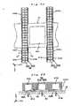
- the reticle stage device 12is provided with a reticle stage supporting plate 16 as a supporting plate that is arranged substantially in parallel at a predetermined space under the illumination system side plate 14, a reticle stage RST as a slider arranged between the reticle stage supporting plate 16 and the illumination system side plate 14, a frame-shaped member (weight portion) 18 that is arranged between the reticle stage supporting plate 16 and the illumination system side plate 14 in a state in which it surrounds the reticle stage RST, a reticle stage drive system that drives the reticle stage RST, etc.
- a reticle stage supporting plate 16as a supporting plate that is arranged substantially in parallel at a predetermined space under the illumination system side plate 14
- a reticle stage RSTas a slider arranged between the reticle stage supporting plate 16 and the illumination system side plate 14
- a frame-shaped member (weight portion) 18that is arranged between the reticle stage supporting plate 16 and the illumination system side plate 14 in a state in which it surrounds the
- the reticle stage supporting plate 16is substantially horizontally supported by an undepicted support member.
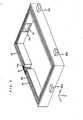
- Fig. 3which is an exploded perspective view of Fig. 2
- the reticle stage supporting plate 16is formed of an approximately plate-shaped member and having a protrusion 16a formed substantially in its center.
- a rectangular opening 16bwhich has the X axis direction as its longitudinal direction and allows the illumination light 1L to pass through, is formed to extend from the upper surface of the protrusion 16a to the lower surface of the reticle stage supporting plate 16.
- Fig. 3is an exploded perspective view of Fig. 2
- the reticle stage supporting plate 16is formed of an approximately plate-shaped member and having a protrusion 16a formed substantially in its center.
- a rectangular opening 16bwhich has the X axis direction as its longitudinal direction and allows the illumination light 1L to pass through, is formed to extend from the upper surface of the protrusion 16a to the lower surface of the reticle stage supporting plate 16.
- an upper end of a lens barrel portion of the projection optical system PLis connected to the lower surface side of the reticle stage supporting plate 16 via the seal member 98, such as a V ring or an extensible bellows, in a state in which the upper end of a lens barrel portion surrounds the rectangular opening 16b.
- the seal member 98such as a V ring or an extensible bellows
- the reticle stage RSTis provided with a specially shaped reticle stage main body 22 shown in Fig. 4A , various magnetic pole units (that will be described later) fixed to the reticle stage main body 22, etc.
- the reticle stage main body 22is provided with a substantially rectangular plate-shaped portion 24A as seen from a top plan view, a mirror portion 24B arranged on the -X end portion of the plate-shaped portion 24A, and respective pairs of extensions 24C 1 , 24C 2 , 24D 1 , 24D 2 extending in the Y axis direction from the end portions of one side and the other side, respectively, of the Y axis direction of the plate-shaped portion 24A.
- an opening 22a with a stepis formed and defines a passage of the illumination light IL in the middle (inside bottom surface).
- a plurality of (e.g., three) reticle support members 34 that support the reticle R at a plurality of points (e.g., three points) from the lower sideare arranged.
- the reticle Ris supported by the plurality of support members 34 in a state in which the pattern surface (lower surface) substantially matches a neutral plane CT of the reticle stage main body 22 (reticle stage RST). That is, the mounting surface (mounting portion) of the reticle R substantially matches the neutral plane CT of the reticle stage RST (see Fig. 4B ).
- each reticle fixing mechanism 36has an XZ cross section with an L shape, and is provided with a fixing member that is mounted on the plate-shaped portion 24A that is rotatable about an axis (rotation axis in the Y axis direction) arranged on the corner of the L shape.
- the respective fixing membersare rotably driven in a predetermined direction via an undepicted drive mechanism driven by the stage control system 90 of Fig.
- various chuckssuch as a vacuum chuck, an electrostatic chuck, etc., can also be used.
- the mirror portion 24Bhas approximately a prismatic shape that has the Y axis direction as a longitudinal direction.
- a bar-shaped portion 124aIn the middle, excluding both end portions in the longitudinal direction of the bar-shaped portion 124a, are provided a bar-shaped portion 124a, in which a round-shaped hollow portion CH (see Fig. 4A ) is formed to improve lightness, and a solid reinforcement portion 124b integrally formed on the +X side of the portion.
- the end surface of the -X side of the bar-shaped portion 124ais made to be a reflective surface (reflective member) 124m on which mirror surface processing has been performed.
- the mirror portion 24B and the plate-shaped portion 24Aare locally connected by hinge portions 124c, 124d shown in Fig. 5A .
- the reticle stage main body portion 22 including the plate-shaped portion 24A, the-mirror portion 24B, and the hinge portions 124c, 124dis integrally molded (e.g., molded by cutting them from one member); however, the following explanation uses an expression in which each part is a different member in order to make the description more easily understood.
- one of the above-mentioned partscan be constituted by a separate member; or all the parts can be constituted by different members.
- the mirror portion 24Bis connected to the -X side end portion of the plate-shaped portion 24A via the hinge portions 124c, 124d, i.e., rotation fulcrums, arranged at the two locations on the ⁇ Y side surface of the reinforcement portion 124b.
- CS connecting the two hinge portions 124c, 124dis a neutral plane when the mirror portion 24B is curved within the horizontal plane.
- a similar type of hinge portion 124eis arranged in a position separated from hinge portion 124c, of the two hinge portions 124c, 124d, by a predetermined distance in the +X direction.
- a portion 124f between the hinge portion 124c and the hinge portion 124eis partially deformed so as to be rotated about the hinge portion 124c, so the effects due to the deformation of the plate-shaped portion 24A with respect to the reflective surface 124m of the mirror portion 24B can be minimized. That is, the portion 124f sandwiched by the hinge portions 124c, 124e functions as a type of flexure.
- Retro reflector 32 1 , 32 2are arranged on the concave portions 24g 1 , 24g 2 , respectively.
- the four extensions 24C 1 , 24C 2 , 24D 1 , 24D 2have a substantially plate shape.
- Triangle-shaped reinforcement portionsare arranged on the respective extensions in order to improve the strength.
- a first gas hydrostatic pressure bearingis formed over the entire area from the extension 24C 1 to the extension 24D 1 in the Y axis direction.
- a second gas hydrostatic pressure bearingis formed over the area from the extension 24C 2 to the extension 24D 2 in the Y axis direction.
- Fig. 6Ashows a plan view (bottom surface view) viewing the reticle stage main body 22 from the lower surface side.
- three groovesare formed on the bottom surface of the reticle stage main body 22 in the areas including the extensions 24C 1 , 24D 1 , and the portion therebetween.
- the groove positioned in the center of the X axis directionis an air supply groove 56 constituted by a stem groove 55A extended in the Y axis direction and a plurality of T-shaped surface restriction grooves 55B connected on both X axis direction sides of the stem groove 55A, and spaced from each other in the Y axis direction at a predetermined interval.
- Fig. 6Bwhich is a D-D cross-sectional view of Fig. 6A
- the stem groove 55Ais formed more deeply than the surface restriction grooves 55B.
- the two remaining grooves of the three groovesare exhaust grooves 57A, 57B extended in the Y axis direction.
- the exhaust grooves 57A, 57Bhave substantially the same cross-sectional shape as that of the stem groove 55A.
- Fig. 6BOn the reticle stage supporting plate 16 opposite to at least part of the respective three grooves 56, 57A, 57B, on the top surface of the protrusion portion 16a, three openings (58, 59A, 59B) are respectively formed.
- the opening positioned in the centeris an air supply port 58
- the openings positioned on both endsare exhaust ports 59A, 59B.
- the air supply port 58is connected to an undepicted gas supply device via an air supply duct 60 shown in Fig. 6B .
- a noble gassuch as helium or a low absorption gas such as nitrogen is supplied from the gas supply device.
- the exhaust ports 59A, 59Bare connected to an undepicted vacuum pump via exhaust ducts 61A, 61B.
- the low absorption gaswhen a low absorption gas is supplied from an undepicted gas supply device via the air supply duct 60, as shown in Fig. 6B , the low absorption gas is supplied to the stem groove 55A of the air supply groove 56 from the air supply port 58 and is spread to the entire area in the Y direction of the stem groove 55A.
- the low absorption gasis further supplied, the low absorption gas is blown from the plurality of surface restriction grooves 55B of the air supply groove 56 against the top surface of the reticle stage supporting plate 16.
- a hydrostatic pressure(so-called pressure within a gap) of a pressurized gas within the gap is constant, and a clearance of, e.g., approximately several ⁇ m is formed and maintained between the reticle stage RST and the reticle stage supporting plate 16.
- a first differential exhaust type gas hydrostatic pressure bearingis substantially constituted in which a pressurized gas from an undepicted gas supply device is supplied by the reticle stage supporting plate 16 without going through piping.
- a supply groove 56 constituted by the above-mentioned stem groove 55A and the plurality of surface restriction grooves 55B, and exhaust grooves 57A, 57B on both sidesare formed.
- a second differential exhaust type gas hydrostatic pressure bearingis substantially constituted in which a pressurized gas from an undepicted gas supply device is supplied from the reticle stage supporting plate 16 without going through piping.
- the reticle stage RSTis floatingly supported in a non-contact state by a balance between a hydrostatic pressure of a pressurized gas, blown via the top surface of the reticle stage supporting plate 16 from the surface restriction grooves 55B of the first and second differential exhaust type gas hydrostatic pressure bearings, and the weight of the entire reticle stage RST, via an approximately several micron clearance above the top surface of the reticle stage supporting plate 16.
- substantially annular concave grooves 83, 85are formed side by side.
- a plurality of air supply ports(undepicted) are formed in the inside annular concave groove 83.
- a plurality of exhaust portsin the outside annular concave groove 85, a plurality of exhaust ports (undepicted) are formed in the inside annular concave groove 83.
- the inside annular concave groove 83is called “air supply groove 83”
- the outside annular concave groove 85is called “exhaust groove 85”.
- the air supply port formed inside the air supply groove 83is connected to an undepicted gas supply device that supplies nitrogen or a low absorption gas such as a noble gas via an undepicted air supply duct and an undepicted air supply tube. Furthermore, the exhaust ports formed inside the exhaust groove 85 are connected to an undepicted vacuum pump via an undepicted exhaust duct and an undepicted exhaust tube.
- annular concave grooves 82, 84are formed side by side.
- annular concave groove 82 located insidea plurality of air supply ports (undepicted) are formed.
- annular concave groove 84 located outsidea plurality of exhaust ports (undepicted) are formed.
- air supply groove 82air supply groove 82
- exhaust groove 84exhaust groove 84
- the air supply ports formed inside the air supply groove 82are connected to an undepicted gas supply device that supplies nitrogen or a low absorption gas such as a noble gas via an air supply duct or an air supply tube. Furthermore, the exhaust ports formed inside the exhaust groove 84 are connected to an undepicted vacuum pump via an exhaust duct or an exhaust tube.
- a pressurized gas(low absorption gas) is blown against the top surface of the reticle stage supporting plate 60 from the air supply groove 82 formed on the bottom surface of the frame-shaped member 18.
- the weight of the frame-shaped member 18is supported by a hydrostatic pressure of the blown pressurized gas, and the frame-shaped member 18 is floatingly supported via an approximately several ⁇ m clearance above the top surface of the reticle stage supporting plate 16.
- the gas within the clearanceis output to the outside by a suction force of the vacuum pump via the exhaust groove 84.
- a gas flowis generated from the air supply groove 82 to the exhaust groove 84. Because of this, it effectively prevents outside air from entering the frame-shaped member 18 via the clearance.
- a differential exhaust type gas hydrostatic pressure bearingis substantially constituted that floatingly supports the frame-shaped member 18 above the top surface of the reticle stage supporting plate 16.
- a pressurized gas(low absorption gas) is blown to the lower surface of the illumination system side plate 14 from the air supply groove 83 formed on the top surface of the frame-shaped member 18.
- gas within a clearance between the illumination system side plate 14 and the frame-shaped member 18is output to the outside by a suction force of the vacuum pump via the exhaust groove 85.
- a gas flowis generated from the air supply groove 83 to the exhaust groove 85. Because of this, it effectively prevents outside air from entering the frame-shaped member 18 via the clearance.
- a clearance between the frame-shaped member 18 and the illumination system side plate 14is maintained by a balance between a hydrostatic pressure of the blown pressurized gas and the vacuum suction force. That is, a differential exhaust type gas hydrostatic pressure bearing that maintains the clearance between the frame-shaped member 18 and the illumination system side plate 14 is substantially constituted by the entire top surface of the frame-shaped member 18.
- the above-mentioned clearance (i.e., bearing gap) between the frame-shaped member 18 and the reticle stage supporting plate 16is actually determined by the overall balance between the force that the differential exhaust type gas hydrostatic pressure bearings above and below the frame-shaped member 18 apply to the frame-shaped member 18 and the entire weight of the frame-shaped member 18.
- the clearance between the frame-shaped member 18 and the illumination system side plate 14 and the clearance between the reticle stage supporting plate 16 and the frame-shaped member 18are made airtight by the gas flow. Furthermore, as described before, the upper end portion of the projection optical system unit PL and the reticle stage supporting plate 16 are connected by the above-mentioned seal member 98 (see Figs. 7 and 8 ). Therefore, the space surrounded by the frame-shaped member 18 has extreme airtightness. Hereafter, the space surrounded by the frame-shaped member 18 is called an "airtight space".
- an absorption gassuch as oxygen
- air in an optical path between the illumination unit IOP and the projection optical system PL, i.e., (the optical path) within the above-mentioned airtight spaceneeds to be replaced with nitrogen or a noble gas.
- an air supply tube and an exhaust tubecan be respectively connected to the side walls of the frame-shaped member 18, a low absorption gas can be supplied to the above-mentioned airtight space via the air supply tube, and an inside gas can be emitted to the outside via the exhaust tube.
- nitrogen or a noble gasis supplied to the airtight space by flowing part of nitrogen or a noble gas that flows, through an undepicted air supply tube connected to the frame-shaped member 18, through the airtight space via an air supply stem tube branched out from part of the air supply duct within the frame-shaped member 18.
- nitrogen or a noble gasis supplied to the airtight space by flowing part of nitrogen or a noble gas that flows, through an undepicted air supply tube connected to the frame-shaped member 18, through the airtight space via an air supply stem tube branched out from part of the air supply duct within the frame-shaped member 18.
- a helium gasis used as gas to be supplied to an airtight space, after a helium gas is collected via a gas exhaust mechanism, and impurities are removed, it is desirable that it is used again.
- the reticle stage drive systemis provided with a first drive mechanism that is constituted by a pair of stator units (pair of stators) 36, 38 that respectively extend in the Y axis direction inside the frame-shaped member 18, that drives the reticle stage RST in the Y axis direction, and micro-drives the reticle stage RST in the ⁇ z direction (rotation direction about the Z axis), and a second drive mechanism that is constituted by a stator unit 40 extended in the Y axis direction on the +X side of stator unit 38 inside the frame-shaped member 18 and that micro-drives the reticle stage RST in the X axis direction.
- a first drive mechanismthat is constituted by a pair of stator units (pair of stators) 36, 38 that respectively extend in the Y axis direction inside the frame-shaped member 18, that drives the reticle stage RST in the Y axis direction, and micro-drives the reticle stage RST in the ⁇ z direction (rotation direction
- the stator unit 36is provided with Y axis linear guides 136 1 , 136 2 as a pair of first stators formed of an armature unit having the Y axis direction as a longitudinal direction, and a pair of fixing members (holding portions) 152 that holds the Y axis linear guides 136), 136 2 with one end portion and the other end portion in the Y axis direction (longitudinal direction).
- the pair of fixing members 152the Y axis linear guides 136 1 , 136 2 are held parallel to the XY plane, and parallel to each other and spaced apart from each other with a predetermined spacing in the Z axis direction (up and down direction).
- the pair of fixing members 152are respectively fixed to inner wall surfaces at one side and the other side (inner surface of the side walls) in the Y axis direction of the frame-shaped member 18.
- the Y axis linear guides 136 1 , 136 2are provided with a frame formed of a non-magnetic material and having a cross section that is rectangular (rectangle). Inside the frame, a plurality of armature coils are arranged at a predetermined interval in the Y axis direction.
- the stator unit 38is constituted in the same manner as the stator unit 36. That is, the stator unit 38 is provided with Y axis linear guides 138 1 , 138 2 as a first stator formed of a pair of armature unit having the Y axis direction as a longitudinal direction, and a pair of fixing members (holding portion) 154 fixed to both end portions in a state wherein the Y axis linear guides 138 1 , 138 2 are maintained at a predetermined interval in the Z axis direction.
- the pair of fixing members 154are fixed to the inner wall surfaces of one side and the other side in the Y axis direction of the frame-shaped member 18.
- the Y axis linear guides 138 1 , 138 2are constituted in the same manner as the Y axis linear guides 136 1 , 136 2 (see Fig. 7 ).
- the reticle stage RSTis arranged between the Y axis linear guides 138 1 , 138 2 and the Y axis linear guides 136 1 , 136 2 , respectively, via the respective predetermined clearances.
- Magnetic pole units 26 1 , 26 2are respectively embedded as a pair of first movable elements on the upper and lower surfaces of the reticle stage RST, facing the Y axis linear guides 136 1 , 136 2 , respectively.
- Magnetic pole units 28 1 , 28 2are respectively embedded as a pair of first movable elements on the upper and lower surfaces of the reticle stage RST, facing the Y axis linear guides 138 1 , 138 2 , respectively.
- the respective magnetic pole units 26 1 , 26 2are arranged within concave portions 24e 1 , 24e 2 that are respectively formed on the upper and lower side surfaces, symmetrically with respect to the neutral plane CT of the reticle stage main body 22.
- the Y axis linear guides 136 1 , 136 2are positioned substantially symmetrically with respect to the neutral plane CT.
- the pair of magnetic pole units 26 1 , 26 2are respectively provided with a magnetic body member and a plurality of field magnets arranged on the surface of the magnetic body member at a predetermined interval along the Y axis direction.
- the plurality of field magnetsare reverse-polarized with respect to each other. Therefore, an alternating field is formed along the Y axis direction in the space above the magnetic pole unit 26 1 , and an alternating field is formed along the Y axis direction in the space below the magnetic pole unit 26 2 .
- the pair of magnetic pole units 28 1 , 28 2are arranged within concave portions 24f 1 , 24f 2 that are respectively formed on the upper/lower surface sides, symmetrically with respect to the neutral surface CT of the reticle stage main body 22.
- the pair of magnetic pole units 28 1 , 28 2are arranged substantially symmetrical to the pair of magnetic pole units 26 1 , 26 2 with respect to the X axis that passes through a center position (substantially matching the X axis direction position of the center of gravity of the reticle stage RST) of the X axis direction of the opening 22a with a step.
- Y axis linear guides 138 1 , 138 2are positioned substantially symmetrically with respect to the neutral plane CT.
- the pair of magnetic pole units 28 1 , 28 2are each provided with a magnetic body member and a plurality of field magnets arranged on the surface of the magnetic body member at a predetermined interval along the Y axis direction.
- a plurality of field magnetsare reverse-polarized with respect to each other. Therefore, an alternating field is formed along the Y axis direction in the space above the magnetic pole unit 28 1 , and an alternating field is formed along the Y axis direction in the space below the magnetic pole unit 28 2 .
- the first drive mechanismis constituted by the above-mentioned stator units 36, 38 (including two pairs of Y axis linear guides 136 1 , 136 2 ,138 1 , 138 2 ) and two pairs of magnetic pole units 26 1 , 26 2 , 28 1 , 28 2 .
- this first drive mechanismby supplying an electric current to armature coils within the Y axis linear guides 136 1 , 136 2 , an electromagnetic force (Lorentz force) in the Y axis direction is generated by electromagnetic interaction between a magnetic field generated by the magnetic pole units 26 1 , 26 2 , and an electric current that goes through the armature units 136 1 , 136 2 .
- the Lorentz forcesbecome a drive force that drives the magnetic pole units 26 1 , 26 2 (reticle stage RST) in the Y axis direction.
- an electromagnetic force (Lorentz force) in the Y axis directionis generated by electromagnetic interaction between a magnetic field generated by the magnetic pole units 28 1 , 28 2 and an electric current that flows through the Y axis linear guides 138 1 , 138 2 .
- the Lorentz forcesbecome a drive force that drives the magnetic pole units 28 1 , 28 2 (reticle stage RST) in the Y axis direction.
- the magnetic pole units 26 1 , 26 2 and the magnetic pole units 28 1 , 28 2are arranged symmetrically with respect to the neutral plane CT of the reticle stage RST.
- the Y axis linear guides 136 1 , 136 2 corresponding to these magnetic pole units and the Y axis linear guides 138 1 , 138 2are also arranged symmetrically with respect to the neutral plane CT.
- the same drive forceis given to the magnetic pole units 26 1 , 26 2 , 28 1 , 28 2 , respectively, so the drive force (the resultant force of the drive forces of the magnetic pole units 26 1 , 26 2 , and the resultant force of the drive forces of the magnetic pole units 28 1 , 28 2 ) in the Y axis direction can be caused to act through the neutral plane CT (see Fig. 4B ) of the reticle stage RST; thus, a pitching moment can be suppressed, to a great degree, from acting on the reticle stage RST.
- the magnetic pole units 26 1 , 26 2 and the magnetic pole units 28 1 , 28 2are arranged substantially symmetrically with respect to the vicinity of the center of gravity position of the reticle stage RST in the X axis direction as well, so the drive force in the Y axis direction can be caused to act on two locations at the same distance from the center of gravity of the reticle stage RST; thus, by generating the same force at the two locations, the resultant force of the drive forces in the Y axis direction can be caused to act on the vicinity of the center of gravity position of the reticle stage RST. Therefore, a yawing moment can be suppressed, to a great degree, from acting on the reticle stage RST.
- yawing of the reticle stage RSTcan be controlled by having different drive forces in the Y axis direction that extends rightward and leftward.
- a pair of moving magnet type Y axis linear motors that drives the reticle stage RST in the Y axis directionis constituted by the magnetic pole units 26 1 , 26 2 , and the linear guides 136 1 , 136 2 corresponding thereto.
- a pair of moving magnet type Y axis linear motors that drives the reticle stage RST in the Y axis directionis constituted by the magnetic pole units 28 1 , 28 2 , and the Y axis linear guides 138 1 , 138 2 corresponding thereto.
- Y axis linear motorsare also described as “Y axis linear motors 136 1 , 136 2 , 138 1 , 138 2 ".
- the above-mentioned first drive mechanismis constituted by the respective pairs of Y axis linear motors 136 1 , 136 2 , and 138 1 , 138 2 .
- the stator unit 40is provided with armature units 140 1 , 140 2 as a pair of second stators that have the Y axis direction as a longitudinal direction, and a pair of fixing members 156 holding the armature units 140 1 , 140 2 at one end portion and the other end portion in the Y axis direction (longitudinal direction).
- the pair of fixing members 156by the pair of fixing members 156, the armature units 140 1 , 140 2 are held parallel to the XY plane and opposite to each other at a predetermined interval in the Z axis direction (vertical direction).
- the pair of fixing members 156are fixed to one side and the other side in the Y axis direction to the inner wall surface of the frame-shaped member 18.
- the armature units 140 1 , 140 2are provided with a frame formed of a non-magnetic material and have a cross section that is rectangular (rectangle), and the armature coils are arranged therein.
- a permanent magnet 30 as a second movable element fixed to the end portion in the X axis direction of the reticle stage RSTis arranged with a predetermined clearance.
- the permanent magnet 30is plate-shaped and has a rectangular (rectangle) cross section.
- a magnetic pole unitalso can be used that is formed of a flat plate-shaped magnet body member and a pair of flat plate-shaped permanent magnets that are respectively fixed to the upper and lower surfaces.
- the permanent magnet 30, and the armature units 140 1 , 140 2are arranged and shaped substantially symmetrically with respect to the neutral plane CT (see Figs. 4B and 7 ).
- an electromagnetic force (Lorentz force) in the X axis directionis generated by electromagnetic interaction between a magnetic field in the Z axis direction formed by the permanent magnet 30 and an electric current that flows in the Y axis direction through the armature coils that constitute the armature unit 140 1 , 140 2 , respectively.
- the Lorentz forcesbecome a drive force that drives the permanent magnet 30 (reticle stage RST) in the X axis direction.
- the drive force in the X axis directioncan be caused to act through the position at the neutral plane CT (see Fig. 4B ) of the reticle stage RST.
- a rolling momentcan be suppressed, to a great degree, from acting on the reticle stage RST.
- a moving magnet type voice coil motoris constituted that can micro-drive the reticle stage RST in the X axis direction.
- this voice coil motoralso is called a movable element that constitutes the voice coil motor, i.e., it is also called "voice coil motor 30," using the reference number of the permanent magnet.
- the second drive mechanismis constituted by the voice coil motor 30.
- movable elements 60 1 , 60 2 , 60 3 formed of magnetic pole unitsare arranged. Attached to the reticle stage supporting plate 16 by members 64 1 , 64 2 and 64 3 , and corresponding to the movable elements (first part) 60 1 , 60 2 , 60 3 , stators (second part) 62 1 , 62 2 , 62 3 are arranged that are formed of armature units.
- the movable elements 60 1 , 60 2are provided with permanent magnets inside and form a magnetic field in the Z axis direction.
- the stators 62 1 , 62 2are provided with armature coils inside, and an electric current flows in the Y axis direction due to the magnetic field in the Z axis direction. Therefore, by supplying an electric current in the Y axis direction to the armature coils within the stators 62 1 , 62 2 , the drive force (generated by Lorentz force) can be caused to act on the movable elements 60 1 , 60 2 in the X axis direction.
- an X axis direction driving trim motor that is formed by a moving magnet type voice coil motoris constituted by the movable element 60 1 and the stator 62 1 .
- An X axis direction driving trim motor that is formed of a moving magnet type voice coil motoris constituted by the movable element 60 2 and the stator 62 2 .
- the movable element 60 3is provided with a permanent magnet inside and forms a magnetic field in the Z axis direction.
- the stator 62 3is provided with an armature coil inside, and an electric current flows in the Y axis direction due to the magnetic field in the Z axis direction.
- the drive forcegenerated by Lorentz force
- a Y axis direction driving trim motorthat is formed by a moving magnet type voice coil motor is constituted by the movable element 60 3 and the stator 62 3 .
- the frame-shaped member 18can be driven in the three degrees-of-freedom directions, i.e., the X axis direction, the Y axis direction, and the ⁇ z direction.
- a concave portion 18ais formed.
- a rectangular opening 18bis formed that is connected to the inside and the outside of the frame-shaped member 18.
- a window glass (transparent portion) g 1is mounted.
- a rectangular opening 18cis formed that is connected to the inside and the outside of the frame-shaped member 18.
- a window glass (transparent portion) g 2is mounted.
- Sealing by a metal seal such as indium or copper, or sealing by a fluororesinis performed over the mounting portion of the window glasses g 1 , g 2 so that gas does not leak from the mounting part.
- a fluororesinshould be heated at 80°C for two hours and undergo degassing processing.
- an X axis laser interferometer 69Xwhich is a position detector, is arranged opposite to the reflective surface 124m of the mirror portion 24B of the reticle stage RST.
- the length measurement beam from the X axis laser interferometer 69Xis projected onto the reflective surface 124m of the mirror portion 24B via the window glass g 1 , and the reflected light returns to the X axis laser interferometer 69X via the window glass g 1 .
- the position of the optical path of the length measurement beam in the Z axis directionmatches the position of the neutral plane CT.
- a fixing mirror Mrxis arranged in the vicinity of the upper end portion of the lens barrel of the projection optical system PL via a mounting member 92.
- a reference beam from the X axis laser interferometer 69Xis projected onto the fixing mirror Mrx via a through hole (optical path) 71 formed on the reticle stage supporting plate 16, and the reflected light returns to the X axis laser interferometer 69X.
- the reflected light of the length measurement beam and the reflected light of the reference beamare composed into coaxial light of the same polarization direction by the optical system, and the interference light of the reflected light beams is received by the detector inside.
- the X axis laser interferometer 69Xconstantly detects the position of the reticle stage main body 22 in the X axis direction at a resolution of, e.g., approximately 0.5-1nm, using the fixing mirror Mrx as a reference.
- a Y axis laser interferometer 69Ywhich is a position detector, is arranged opposite to the reflective surface of the retro reflectors 32 1 , 32 2 arranged in the reticle stage main body 22.
- a pair of Y axis laser interferometers 69Yare arranged corresponding to the respective retro reflectors 32 1 , 32 2 .
- the length measurement beams from the respective Y axis laser interferometers 69Yare projected onto the reflective surfaces of the respective retro reflectors 32 1 , 32 2 via the window glass g 2 .
- the respective reflected light beamsreturn to the respective Y axis laser interferometers 69Y via the window glass g 2 .
- the position of the irradiation point of the length measurement beam in the Z axis directionsubstantially matches the position of the neutral plane CT.
- a fixing mirror Mryis arranged via a mounting member 93.
- the reference beam for the respective Y axis laser interferometers 69Yare respectively projected onto the fixing mirror Mry via a through hole (optical path) 72 formed on the reticle stage supporting plate 16.
- the respective reflected light beamsreturn to the respective Y axis laser interferometers 69Y.
- the respective Y axis laser interferometers 69Yconstantly detect the position of the reticle stage main body 22 in the Y axis direction at the projection position (position of the reflective surfaces of the retro reflectors 32 1 , 32 2 ) of the respective length measurement beams at a resolution of, e.g., approximately 0.5-1nm, with the fixing mirror Mry as a reference, based on the interference light of the reflected light of the length measurement beam and the reflected light of the reference beam.
- the rotation amount about the Z axis of the reticle stage RSTalso can be detected by the pair of Y axis laser interferometers 69Y.
- the mirror portion 24Bis arranged outside of the stator unit 36 (Y axis linear motors 136 1 , 136 2 ). Because of this, the length measurement beam of the X axis laser interferometer 69X is not transmitted above the stator of the Y axis linear motors 136 1 , 136 2 , so heat generated by an electric current that flows through the stator of the Y axis linear motors 136 1 , 136 2 does not affect a measurement value of the X axis laser interferometer 69X due to air fluctuation, even if air fluctuation is generated in the vicinity of the Y axis linear motors 136 1 , 136 2 .
- the X axis direction position of the reticle stage RST, and in turn, the reticle Rcan be detected with high accuracy.
- the position of the optical path of the length measurement beam of the X axis laser interferometer 69X in the Z axis directionmatches the position of the neutral plane CT, and the mounting surface of the reticle R also matches the neutral plane CT; thus, the X axis direction position of the reticle stage RST, and in turn, the reticle R can be accurately measured without so-called Abbe's errors.
- the Y axis direction position of the reticle stage RSTthat is, the reticle R
- the Y axis direction position of the reticle stage RSTcan be accurately measured without so-called Abbe's errors.
- the above-mentioned X axis laser interferometer 69X and the pair of Y axis interferometers 69Yare arranged outside of the frame-shaped member 18, so the highly likely problems caused by having each interferometer arranged inside the frame-shaped member 18 can be suppressed. For example, even if a small amount of absorption gas is generated from a detector such as a prism and an optical member that constitutes each interferometer, this does not leak a low absorption gas into the above-mentioned airtight space, and there will be no negative effect on exposure.
- the mirror portion 24B, and the reticle reflectors 32 1 , 32 2are provided as moving mirrors. Accordingly, the X axis laser interferometer 69X and the pair of Y axis laser interferometer 69Y are provided. However, in Fig. 1 , the reticle moving mirror Mm and the reticle interferometer system 69 are depicted. Furthermore, in Fig. 1 , the fixing mirrors (fixing mirror M rx , fixing mirror M ry ) are omitted.
- the position (including the ⁇ z rotation) within the XY plane of the reticle stage RSTis measured by the reticle interferometer system 69.
- the positional information (or speed information) of the reticle stage RST from this reticle interferometer system 69is sent to the stage control system 90 of Fig. 1 , and to the main controller 70 via the stage control system 90.
- the stage control system 90according to the instructions from the main controller 70, based on the positional information (or speed information) of the reticle stage RST, the drive of the reticle stage RST is controlled.
- the projection optical system PLa reduction system that is both-side-telecentric and a dioptric system formed of a plurality of lens elements having a common Z axis direction optical axis are used.
- this projection optical system PLis held by an undepicted holding member via a flange portion FLG arranged on the lens barrel portion of the projection optical system PL.
- the projection magnification ß of the projection optical system PLis, for example, 1/4 or 1/5.
- the circuit pattern within the illumination area formed on the reticle Ris reduced and projected onto the irradiation area (exposure area) of the illumination light IL on the wafer conjugate to the illumination area by the projection optical system PL, and a reduced image (partial inverted image) of the circuit pattern is transferred and formed.
- the lens barrel of the projection optical system PLis connected to one end of an air supply duct 50 and one end of an exhaust duct 51.
- the other end of the air supply duct 50is connected to an undepicted supply device of a low absorption gas, e.g., a helium gas supply device.
- the other end of the exhaust duct 51is connected to an external gas recovery device.
- a highly purified helium gas from the helium gas supply deviceflows through the inside of the lens barrel of the projection optical system unit PL via the air supply duct 50. In this case, a helium gas is collected in the gas recovery device.
- helium gasis used as the low absorption gas, in addition to the same reason mentioned above, is that fluorite, which has a large thermal expansion coefficient, is used as a lens material of the projection optical system PL, and upon considering that the temperature increase generated by the lens absorbing the illumination light IL deteriorates an imaging characteristic of the lens, using helium gas, which is a low absorption gas with a significant cooling effect, is desirable.
- the wafer stage WSTis arranged within a wafer chamber 80.
- This wafer chamber 80is formed by a partition wall 71 in which a round opening 71a is formed substantially in the center portion of a ceiling portion.
- This partition wall 71is formed of a material with little degassing such as stainless (SUS).
- the lower end portion of the lens barrel of the projection optical system unit PLis inserted to the opening 71 a of the ceiling portion of the partition wall 71.
- the surrounding of the opening 71 a of the ceiling wall of the partition wall 71 and the flange portion FLG of the projection optical system unit PLare connected by a flexible bellows 97 without any space therebetween.
- the gas within the wafer chamber 80is isolated from the outside.
- a stage base BSis substantially horizontally supported via a plurality of vibration isolation units 86.
- the plurality of vibration isolation units 86insulate the stage base BS from micro vibration (background vibration) that is transmitted to the stage base BS from the floor F, e.g., at a micro G level.
- micro vibrationbackground vibration
- active vibration isolation devicesalso can be used in which the stage base BS is positively damped based on the output of vibration sensors, such as semiconductor accelerometers, that are fixed to part of the stage base BS.
- the wafer stage WSTholds the wafer W by vacuum adsorption, etc. via a wafer holder 25 and is freely driven in the XY two-dimensional direction along the top surface of the base BS by an undepicted wafer drive system, including, e.g., a linear motor, etc.
- an undepicted wafer drive systemincluding, e.g., a linear motor, etc.
- the space of the optical path from the projection optical system unit PL to the wafer Wneeds to be replaced with nitrogen or a noble gas.
- one end of an air supply duct 41 and one end of an exhaust duct 43are respectively connected to the partition wall 71 of the wafer chamber 80.
- the other end of the air supply duct 41is connected to an undepicted supply device of a low absorption gas, e.g., a helium gas supply device.
- the other end of the exhaust duct 43is connected to an external gas recovery device.
- a helium gasconstantly flows through the wafer chamber 80.
- a light transparent window 85is arranged on the side wall of the -Y side of the partition wall 71 of the wafer chamber 80.
- a light transparent windowalso is arranged on the side wall of the +X side (front side of the paper plane of Fig. 1 ) of the partition wall 71.
- These light transparent windowsare constituted by mounting a light transparent member, general optical glass in this embodiment, that seals the window portion to the window portion (opening portion) formed in the partition wall 71.
- sealing by a metal seal such as indium or copper, or sealing by a fluororesinis performed over the mounting portion of the window glasses so that gas does not leak from the mounting part.
- it is desirable that the fluororesinshould be heated at 80°C for two hours and undergo degassing processing.
- a Y moving mirror 56Y formed of a flat mirrorextends in the X axis direction.
- the length measurement beam from a Y axis laser interferometer 57Y arranged outside of the wafer chamber 80is projected substantially perpendicular to the Y moving mirror 56Y via the light transparent window 85, the reflected light is received by a detector inside the Y axis laser interferometer 57Y via the light transparent window 85, and as the position of a reference mirror inside the Y axis laser interferometer 57Y, the position of the Y moving mirror 56Y, i.e., the Y position of the wafer W, is detected.
- an X moving mirror formed of a flat mirrorextends in the Y axis direction. Furthermore, the position of the X moving mirror by the X axis laser interferometer via the X moving mirror, i.e., the X position of the wafer W is detected in the same manner as described above.
- the detection values (measurement values) of the above-mentioned two laser interferometersare supplied to the stage control system 90, and to the main controller 70 via the stage control system 90. In the stage control system 90, based on the instructions of the main controller 70, position control of the wafer stage WST is performed via the wafer drive system while monitoring the detection values of the two laser interferometers.
- a laser interferometeri.e., a laser light source, an optical member such as a prism, a detector, etc., is arranged outside the wafer chamber 80, so even if a small amount of absorption gas is generated from the detector or the like, this does not negatively affect exposure.
- a structurealso can be used in which a helium gas is circulated and used, in which the other end of the air supply duct 50 connected to the lens barrel of the projection optical system PL and the other end of the exhaust duct 51 are respectively connected to an undepicted helium gas supply device, a highly purified helium gas is constantly supplied to the lens barrel of the projection optical system PL via the air supply duct 50 from the helium gas supply device, and gas within the lens barrel returns to the helium gas supply device via the exhaust duct 51.
- a gas purifieris provided in the helium gas supply device.
- the concentrations of absorption gas (oxygen, moisture, organic matter, etc.) other than the helium gas within the projection optical system PLcan be maintained at several ppm or less.
- a sensorsuch as a pressure sensor, an absorption gas concentration sensor, etc., is arranged within the projection optical system PL. Based on the measurement values of the sensor, the activation and stopping of a pump housed in the helium gas supply device can be appropriately controlled via an undepicted controller.
- a circulation route of the same type of helium gasalso can be used for the wafer chamber 80.
- a reticle and a waferare loaded by undepicted reticle and wafer loaders, respectively, under control of the main controller 70. Furthermore, by using a reticle alignment system, a reference mark plate on the wafer stage WST, an off-axis/alignment detecting system (these are not depicted), etc., preparation operations such as base line measurement (measurement of the distance between the detecting center of the alignment detecting system and the optical axis of the projection optical system PL) etc. are performed in a predetermined order.
- alignment measurementsuch as EGA (Enhanced Global Alignment) etc. is performed by the main controller 70, using an undepicted alignment detecting system.
- the stage control system 90moves the wafer stage WST holding the wafer W in a predetermined direction via an undepicted wafer drive system.
- the wafer stage WSTPrior to this exposure operation, first the wafer stage WST is moved so that the XY position of the wafer W becomes a scanning start position (accelerating start position) for exposure of a first shot area on the wafer W. Simultaneously, the reticle stage RST is moved so that the position of the reticle R becomes a scanning start position.
- the stage control system 90synchronously moves the reticle R (reticle stage RST) and the wafer W (wafer stage WST), so scanning exposure is performed.
- the movable element of the voice coil motor 30is driven in the X axis direction, integrally with the reticle stage RST, and the reaction force from this drive force can be caused to act on the stators (armature units 140 1 , 140 2 ) of the voice coil motor 30, and on the frame-shaped member 18 to which the stators are fixed.
- the frame-shaped member 18is in a non-contact state via a predetermined clearance with respect to the reticle stage supporting plate 60 and the illumination system side plate 14, so because of the effect of the reaction force, the frame-shaped member 18 moves in a direction corresponding to the reaction force for a distance according to the law of conservation of momentum. Because of this movement of the frame-shaped member 18, the reaction force is absorbed. At this time, depending on the position of the reticle stage RST in the Y axis direction, a yawing moment due to the reaction force of the drive force in the X axis direction can be caused to act on the frame-shaped member 18. In this case, the frame-shaped member 18 freely moves in ⁇ z rotation so as to absorb a reaction force according to the law of conservation of momentum by the yawing moment and the effect of the reaction force in the X axis direction.
- the respective movable elements of the Y axis linear motors 136 1 , 136 2 , 138 1 , 138 2are driven in the Y axis direction and are integral with the reticle stage RST, and the resultant reaction force from the drive forces of the respective movable elements can be caused to act on the respective stators of the Y axis linear motors 136 1 , 136 2 , 138 1 , 138 2 , and on the frame-shaped member 18, to which these are fixed.
- the frame-shaped member 18moves in a direction corresponding to the resultant reaction force, for a distance by which the resultant reaction force is absorbed.
- the reaction force(the reaction in the X axis direction and the Y axis direction) generated by the driving of the reticle stage RST and the yawing moment generated by the reaction force can be reliably canceled, and the vibration due to the driving of the reticle stage RST can be controlled. Furthermore, the generation of the above-mentioned offset load also can be suppressed, so an attitude change, etc. of the reticle stage supporting plate 16 due to this reason also can be suppressed.
- the main controller 70returns the frame-shaped member 18 to a predetermined reference position. This is done using the above-mentioned three trim motors, via the stage control system 90 when exposure is not performed, so that a shift amount from the reference position does not exceed allowable values (i.e., for example, problems will not occur such that the voice coil motor 30 cannot be controlled because of the movement of the frame-shaped member 18, or outside air enters the airtight space within the frame-shaped member 18 via a gap between the frame-shaped member 18 and the reticle stage supporting plate 16), for example.
- allowable valuesi.e., for example, problems will not occur such that the voice coil motor 30 cannot be controlled because of the movement of the frame-shaped member 18, or outside air enters the airtight space within the frame-shaped member 18 via a gap between the frame-shaped member 18 and the reticle stage supporting plate 16
- the reticle stage RSTcan hold the reticle R while being caused to float above the reticle stage supporting plate 16 and move along the reticle stage supporting plate 16 in three degrees-of-freedom directions within the two-dimensional plane including the Y axis and the X axis perpendicular to the Y axis, and the frame-shaped member 18 has three degrees of freedom within the two-dimensional plane while being caused to float above the reticle stage supporting plate 16.
- the respective stators (linear guides 136 1 , 136 2 , 138 1 , 138 2 ) of the Y axis linear motors 136 1 , 136 2 , 138 1 , 138 2 and stators (armature units 140 1 , 140 2 ) of the voice coil motor 30are arranged.
- the respective movable elements (magnetic pole units 26 1 , 26 2 , 28 1 , 28 2 ) of the Y axis linear motors 136 1 , 136 2 , 138 1 , 138 2 and the movable element (permanent magnet 30) of the voice coil motor 30are arranged on the reticle stage RST.
- the reaction force according to the drive forceis generated in (acts on) the stators (linear guides 136 1 , 136 2 , 138 1 , 138 2 ) or the stators (armature units 140 1 , 140 2 ). Because of the effect of this reaction force, the frame-shaped member 18 moves in three degrees-of-freedom directions within the two-dimensional plane substantially according to the law of conservation of momentum. That is, the frame-shaped member 18 functions as a countermass.
- the reaction forceis substantially completely canceled by the movement of the frame-shaped member 18.
- movement of the center of gravity of the system including the reticle stage RST and the frame-shaped member 18is not generated, so an offset load is not caused to act on the reticle stage supporting plate 16. Therefore, position controllability of the reticle stage RST on which the reticle R is mounted can be improved.
- the frame-shaped member 18is arranged so as to surround the reticle stage RST, so the size naturally becomes large, the mass also becomes large, and a large mass ratio between the frame-shaped member 18 and the reticle stage RST can be obtained; thus, a moving stroke of the frame-shaped member 18 can be relatively short. Furthermore, substantially no problems will occur even when the frame-shaped member 18 needs to be enlarged.
- the surface on which the reticle R is mountedis formed at part of the neutral plane CT, and the position of the optical path of the length measurement beam from the reticle interferometer system 69 in the Z axis direction matches the position of the neutral plane CT. Therefore, unlike the conventional example explained above using Fig. 12B , when the reticle stage RST is deformed, a positional measurement error generated due to the shift between the neutral plane CT and the length measurement axis and a type of Abbe's error due to the positional shift of the length measurement axis and the pattern plane of the reticle R can be made substantially zero. Therefore, the position of the reticle R can be measured with high accuracy.
- the first drive mechanism that drives the reticle stage RSTis provided with the respective pairs of movable elements (magnetic pole units 26 1 , 26 2 , 28 1 , 28 2 ) that are arranged symmetrically with respect to the neutral plane CT, on one side and the other side, in the X axis direction, of the area where the reticle R of the reticle stage RST is mounted, and two pairs of stators (linear guides 136 1 , 136 2 , 138 1 , 138 2 ) that in cooperation with the respective movable elements individually respectively generate drive forces in the Y axis direction.
- a laminated structureis used that is formed of the movable element, the reticle stage main body, and the movable element. Additionally, the movable elements are arranged symmetrically with respect to the neutral plane CT.
- the neutral plane of the reticle stage RSTsubstantially matches the height position of the center of gravity of the reticle stage RST (position in the Z axis direction), so the resultant force of the drive forces in the Y axis direction generated by the cooperation of these pairs of movable elements and stators corresponding thereto can be caused to act on the position of the center of gravity of the reticle stage RST.
- the respective pairs of stators(linear guides 136 1 , 136 2 , 138 1 , 138 2 ) are arranged symmetrically with respect to the neutral plane CT. Therefore, when the reticle stage RST is driven in the Y axis direction along the reticle stage supporting plate 16, even if the reticle stage RST is heated by the heat generation of the linear guides 136 1 , 136 2 , 138 1 , 138 2 by an electric current supplied to the respective armature coils of the linear guides 136 1 , 136 2 , 138 1 , 138 2 , deformation of the reticle stage main body 22 due to the bimetal effect generated on the upper and lower sides of the neutral plane CT is canceled in the heated portion, and the deformation of the reticle stage RST due to the bimetal effect ultimately is not generated.
- the position of the reticle stage RST in the Y axis directionis measured by the pair of the Y axis interferometers 69Y via the pair of retro reflectors 32 1 , 32 2 arranged on the reticle stage RST, and based on the measurement result, the position of the reticle stage RST in the Y axis direction is controlled; thus, the position controllability of the reticle stage RST in the Y axis direction can be performed extremely well.
- the reflective surface to which the length measurement beam in the X axis direction from the reticle interferometer system 69 is irradiatedis arranged outward from the linear motors 136 1 , 136 2 that drive the reticle stage RST in the Y axis direction, so even if temperature fluctuation is generated in a gas near the linear motors due to the heat generated by the linear motors, the length measurement beam in the X axis direction is not affected. Because of this, the positional measurement of the reticle stage RST in the X axis direction by the X axis interferometer 69X can be performed with high accuracy.
- the length measurement beam in the Y axis direction from the reticle interferometer system 69can be irradiated to the reflective surfaces (reflective surfaces positioned at a location where the heat generated by the linear motors is hardly affected) of the retro reflectors 32 1 , 32 2 arranged on the reticle stage RST without any problems occurring. Therefore, the position of the reticle stage RST in the Y axis direction and in the X axis direction can be measured with good accuracy. That is, the positional controllability of the reticle stage RST can be improved.
- the reflective surface 124m to which the length measurement beam in the X axis direction from the reticle interferometer system 69 is irradiatedis formed on the end surface of the bar-shaped mirror portion 24B with a predetermined length different from that of the plate-shaped portion 24A on which the reticle R of the reticle stage RST is mounted, the reinforcement portion 124b is arranged on the portion excluding both end portions in the longitudinal direction of the bar-shaped portion 124a on which the reflective surface 124m of the mirror portion 24B is formed, and both ends of the reinforcement portion 124b are coupled to the plate-shaped portion 24A via the elastic hinge portions 124c, 124d. Because of this, the portion between the elastic hinge portions 124c and 124d of the reflective surfaces, that is, the portion mainly used for position control of the reticle stage RST can be suppressed, to a great degree, from being deformed.
- a structureis used in which: on end portions of one side and the other side of the reticle stage RST in the Y axis direction, extensions 24C 1 -24D 2 extending in the Y axis direction are respectively arranged; on the bottom surface of the reticle stage RST, a gas hydrostatic pressure bearing is formed over the entire area in the longitudinal direction reaching from one side of the extension to the other side of the extension; and a pressurized gas is supplied to the gas hydrostatic pressure bearing from the reticle stage supporting plate 16 without piping. Because of this, the reticle stage RST is not driven in a pipe dragging state, and a thrust needed to maintain a uniform motion is hardly needed during exposure in which the reticle stage performs a uniform motion. Therefore, thrust ripple of the linear motors and other effects are not experienced.
- position controllability of the reticle stage RSTis extremely good. Therefore, synchronization control accuracy between the reticle stage RST and the wafer stage WST can be improved. Because of this, a pattern formed on the reticle R can be transferred onto the wafer W with high accuracy.
- a space including the optical path of the illumination light IL between the illumination unit IOP and the projection optical system PLis a space purged by a low absorption gas (a specified gas whose characteristic of absorbing the illumination light IL is smaller than that of air).
- the frame-shaped member 18is used as a partition wall that divides the purged space from the outside air, so the space around the reticle stage RST can be easily made a purged space. Absorption of the illumination light IL within the purged space can be suppressed to a great degree.
- the first drive mechanism that drives the reticle stage RST in the Y axis directionis constituted by a pair of the Y axis linear motors
- the second drive mechanism that drives the reticle stage RST in the X axis directionis constituted by a voice coil motor, but this invention is not limited to this.
- the hollow portion CHis formed in the mirror portion 24B.
- the mirror portion 24B and the plate-shaped portion 24Awere integrally molded, but the invention is not limited to this.
- These elementscan be constituted by separate members, and each member can be connected by an elastic hinge portion.
- the illumination system side plate 14is arranged above the reticle stage device 12.
- a space in the vicinity of the reticle stage RSTcan be maintained to some degree of airtightness without arranging the illumination system side plate 14, for example, by sealing the top side (illumination system side) of the frame-shaped member while keeping a window portion that transmits illumination light.
- the frame-shaped member 18 surrounding the reticle stage RSTalso is used as a partition wall that divides the space surrounding the reticle stage from the outside air, but this invention is not limited to this.
- the reticle stage RST and the frame-shaped memberare stored in a chamber (reticle stage chamber), and the space surrounding the reticle stage RST also can be replaced with a low absorption gas.
- a predetermined intervalis formed between the frame-shaped member and the reticle stage supporting plate, and the frame-shaped member can be movably constituted within the two-dimensional plane (XY plane).
- XY planetwo-dimensional plane
- stage device of an embodiment of this inventionwas applied to a reticle stage device of a scanning type VUV exposure apparatus, but this invention is not limited to this.
- the stage device of this inventionalso can be suitably applied to a mask stage device of a proximity type aligner that transfers a mask pattern onto a substrate by closely contacting the mask and the substrate without a projection optical system, a mask stage device such as a step-and-repeat transfer type scanning exposure apparatus for liquid crystal, or a plate stage device, etc.
- the stage device of this inventionalso can be applied to an EBPS type electron beam exposure apparatus, and to a so-called EUVL exposure apparatus that uses light of a soft X-ray region as exposure light with a wavelength of approximately 5-30 nm.
- the inventionis not limited to an exposure apparatus, but the stage device of this invention can be suitably applied to other precision machinery, etc.
- vacuum ultraviolet lightsuch as produced by an ArF excimer laser (wavelength 193 nm) or an F 2 laser (wavelength 157 nm), far ultraviolet light, such as produced by a KrF excimer laser (wavelength 248 nm), and bright lines (g line, i line, etc.) of the ultraviolet region produced by an ultra high-pressure mercury lamp can be used as the illumination light IL.
- the inventionis not limited to this.
- Other vacuum ultraviolet lightsuch as an Ar 2 laser (wavelength 126 nm) also can be used.
- vacuum ultraviolet lightis not limited to the above-mentioned laser, but harmonics also can be used in which a single wavelength infrared or visible laser oscillated from a DFB semiconductor laser or a fiber laser is amplified by a fiber amplifier, in which, e.g., erbium (Er) (or both erbium and ytterbium (Yb)) is doped, and wavelength-converted to ultraviolet light by using nonlinear optical crystal.
- erbium (Er)or both erbium and ytterbium (Yb)
- charged particle rayssuch as X rays (including EUV light), or an electron beam, an ion beam, etc. also can be used as illumination light IL.
- the projection optical systemwhen vacuum ultraviolet light, e.g., an Ar 2 laser, is used for the illumination light IL, a so-called catadioptric system that combines refractive optical elements and reflective optical elements (a concave surface mirror, a beam splitter, etc.), or a reflective optical system formed of only reflective optical elements is mainly used, as disclosed in, e.g., Japanese Laid-Open Patent Application 3-282527 , USP 5,220,454 corresponding thereto, Japanese Laid-Open Patent Application 8-171054 , USP 5,668,672 corresponding thereto, Japanese Laid-Open Patent Application 10-20195 , and USP 5,835,275 corresponding thereto. Furthermore, as long as the law of the country that was designated or selected in this International Application allows
- this inventionwas applied to an exposure apparatus for manufacturing a semiconductor, but the invention is not limited to this.
- This inventioncan be broadly applied to an exposure apparatus for liquid crystal that transfers a liquid crystal element pattern onto a square-shaped glass plate, an exposure apparatus for manufacturing a thin film magnetic head, an image pick-up element, an organic EL, a micro-machine, a DNA chip, or the like.
- this inventionalso can be applied to an exposure apparatus that transfers a circuit pattern onto a glass substrate, a silicon wafer, etc.
- a transmissive type reticleis generally used.
- quartz glass, quartz glass in which fluoride is doped, fluorite, magnesium fluoride, or crystal, etc.can be used.
- this inventionalso can be applied to a liquid immersion type exposure apparatus where liquid is filled between the projection optical system PL and the wafer, as disclosed in, e.g., International Publication WO99/49504 .
- Fig. 10shows a flowchart of an example of a process for manufacturing a device (a semiconductor chip such as an IC and an LSI, a liquid crystal panel, a CCD, a thin film magnetic head, a micro-machine, etc.).
- a devicea semiconductor chip such as an IC and an LSI, a liquid crystal panel, a CCD, a thin film magnetic head, a micro-machine, etc.
- step 201design step
- device functions and performance capabilitiesare designed (e.g., design of a circuit of a semiconductor device, etc.), and a pattern is designed that accomplishes the functions.
- step 202mask manufacturing step
- a maskis manufactured on which a designed circuit pattern is formed.
- a wafer manufacturing stepa wafer is manufactured by using a material such as silicon.
- step 204wafer processing step
- step 205device assembly step
- step 205includes a dicing process, a bonding process, a packaging process (chip sealing), etc., as needed.
- step 206(testing step), an operation confirmation test of the device manufactured in step 205, a durability test, etc. are performed. Upon completing these processes, the device is completed and then shipped.
- Fig. 11shows a detailed flowchart of the above-mentioned step 204 in the case of a semiconductor device.
- step 211oxidation step
- step 212CVD step
- step 313electrode formation step
- step 313electrode formation step
- step 214ion embedding step
- ionsare embedded in the wafer.
- the above-mentioned steps 211-214constitute a pre-processing step for each level of the wafer processing, and are selected and performed according to the necessary processing in each level.
- step 215resist formation step
- step 216exposure step
- step 217developing step
- step 218etching step
- step 219resist removing step
- the exposure apparatus of this inventionsuch as the exposure apparatus 10 of the above-mentioned embodiment is used in the exposure step (step 216), a reticle pattern can be transferred onto a wafer with high accuracy. Productivity (including yield) of devices with high integration can be ultimately improved.
- stage devices of this inventionare suitable when an object is mounted and moved.
- exposure apparatus of this inventionare suitable when a pattern formed on a mask is transferred onto a photosensitive object.
- methods of manufacturing a device of this inventionare suitable for manufacturing a micro-device.
Landscapes
- Physics & Mathematics (AREA)
- General Physics & Mathematics (AREA)
- Engineering & Computer Science (AREA)
- Microelectronics & Electronic Packaging (AREA)
- Manufacturing & Machinery (AREA)
- Computer Hardware Design (AREA)
- Condensed Matter Physics & Semiconductors (AREA)
- Power Engineering (AREA)
- Chemical & Material Sciences (AREA)
- Chemical Kinetics & Catalysis (AREA)
- Exposure And Positioning Against Photoresist Photosensitive Materials (AREA)
- Exposure Of Semiconductors, Excluding Electron Or Ion Beam Exposure (AREA)
- Container, Conveyance, Adherence, Positioning, Of Wafer (AREA)
- Linear Motors (AREA)
- Reciprocating, Oscillating Or Vibrating Motors (AREA)
Abstract
Description
- This invention relates to stage devices, exposure apparatus, and methods of manufacturing devices, and more specifically to stage devices provided with a supporting plate and a slider that moves along the supporting plate, exposure apparatus provided with such a stage device, and methods of manufacturing devices using the exposure apparatus.
- Recently, in a lithographic process that manufactures a semiconductor element, a liquid crystal display element, etc., a step-and-scan type scanning exposure apparatus (so-called scanning stepper (scanner)) is relatively frequently used that synchronously moves a mask or a reticle (hereafter referred to as "reticle") and a photosensitive object such as a wafer or a glass plate (hereafter referred to as "wafer") along a predetermined scanning direction (scan direction) and transfers a reticle pattern onto the wafer via a projection optical system. A scanning exposure apparatus can expose a large field with a projection optical system smaller than a stationary type exposure apparatus such as a stepper. Because of this, there are various advantages associated with a scanning exposure apparatus, e.g., manufacturing of a projection optical system is easier, high throughput is expected due to the reduction of number of shots by large field exposure, averaging effects can be seen by scanning a reticle and a substrate relative to a projection optical system, and distortion and depth of focus can be improved.
- Therefore, in a scanning exposure apparatus, a drive device is needed that drives a reticle on the reticle side in addition to the wafer side. In recent scanning exposure apparatus, as a drive device on the reticle side, a reticle stage device with a coarse/micro-moving structure is used that has a reticle coarse-moving stage that is floatingly supported on a reticle supporting plate by an air bearing or the like and is driven in a scanning direction within a predetermined stroke range by a pair of linear motors arranged on both sides in a non-scanning direction perpendicular to a scanning direction, and a reticle micro-moving stage that is micro-moved in a scanning direction, a non-scanning direction, and a yawing direction by a voice coil motor or the like with respect to the reticle coarse-moving stage.
- Furthermore, there also is a reticle stage device in which, in order to suppress the vibration and attitude fluctuation of a reticle support plate that are caused by a reaction force generated in a stator of a linear motor according to driving of a reticle stage, a countermass mechanism is arranged that has a countermass (weight member) that, upon receiving the reaction force, moves according to the law of conservation of momentum, e.g., in a direction opposite to the reticle stage along with a stator (linear guide) of a linear motor that extends in a scanning direction of the reticle stage.
- However, in a reticle stage device used by a conventional scanning exposure apparatus, there are various points that need to be improved as follows:
- a. There is a side guide between a stator carrier that mounts the motor stator for driving the micro-moving stage and a supporting plate; therefore a reaction and a yawing moment at the time of positioning the reticle micro-moving stage (reticle) in a non-scanning direction, and a moment generated at the time of driving the coarse-moving stage, are transmitted to the supporting plate via the side guide, which causes vibration of the supporting plate. As a result, accurate position control (including positioning accuracy) of the reticle is deteriorated.
- b. Wiring for supplying an electric current, piping for vacuum exhaust for a vacuum chuck, piping for supplying pressurized air for an air bearing, etc. were connected to the reticle-micro-moving stage and the reticle coarse-moving stage. Because of this, when the reticle micro-moving stage and the reticle coarse-moving stage were moved, the above-mentioned wiring and piping were dragged, and the tension of the wiring and the piping ultimately caused accurate position control (positioning accuracy) of the reticle to deteriorate.
- c. Mechanical vibration near the reticle micro-moving stage and stage distortion due to heat caused positional measuring errors of the reticle micro-moving stage. As an example, as shown in
Fig. 12A , a case is considered in which the position of a reticle micro-moving stage RST (reticle R) is measured by an interferometer having a length measurement axis LX via a movingmirror 169 arranged on the reticle micro-moving stage RST. In this case, if distortion shown inFig. 12B is generated on the reticle stage RST, the ΔM measuring error (a type of Abbe number) is generated in positional information to be measured by the interferometer. In addition, inFigs. 12A and 12B , symbol CR shows a neutral plane (curved neutral plane) of the reticle micro-moving stage RST. - d. Furthermore, the distortion of the reticle micro-moving stage caused the distortion (curving) of the moving mirror, and accurate position measurement of the reticle micro-moving stage, and in turn, accurate position control was deteriorated.
- e. Furthermore, particularly in a reticle stage device provided with a countermass mechanism, it was difficult to maintain a sufficiently large mass ratio of a countermass (weight member) and a reticle stage. This is because in the above-mentioned conventional countermass mechanism, the countermass needs to have its center of gravity arranged on an axis of a linear guide, so in order to increase the countermass weight, the countermass needs to be extended in an axial direction of the linear guide, or its dimension in a radial direction within an axially perpendicular plane about the linear guide needs to be uniformly increased, so there is naturally a restriction in terms of layout. Thus, it was difficult to sufficiently obtain a mass ratio of the countermass (weight member) and the reticle stage, so the stroke of the countermass became large, effects due to dragging the piping and local body distortion due to center of gravity movement could not be ignored; therefore, position controllability deteriorated.
- f. In addition, the arrangement and the shape of the members near the reticle stage were complex, and the surrounding space was a complex open space; thus, air adjusting efficiency was poor, accurate interferometer measurement, and in turn, the reticle position controllability, deteriorated due to air fluctuation (air temperature fluctuation), etc. Furthermore, when vacuum ultraviolet light such as an F2 laser is used as exposure illumination light, in the vicinity of the reticle as well, a gas purge must be performed that replaces an atmospheric gas with an inert gas, but the above-mentioned arrangement and shape of the members near the reticle stage were complex, so the design was extremely difficult.
- This invention reflects upon the above-mentioned situation. A first object of this invention is to provide a stage device that can improve position controllability of a moving body on which an object is placed.
- A second object of this invention is to provide an exposure apparatus that can accomplish exposure with high accuracy.
- A third object of this invention is to provide a method of manufacturing a device that can improve device productivity with high integration.
- In a first aspect, this invention is a first stage device having a supporting plate; a slider that holds an object while floating above the supporting plate, and that can be moved along the supporting plate in three degrees-of-freedom directions within a two-dimensional plane including a first axis and a second axis perpendicular thereto; a frame-shaped member that moves in at least three degrees-of-freedom directions within the two-dimensional plane while floating above the supporting plate and surrounds the slider; a first drive mechanism that includes a first stator arranged on the frame-shaped member and a first movable element that in cooperation with the first stator generates a drive force that drives the slider in the first axis direction; and a second drive mechanism that includes a second stator arranged on the frame-shaped member and a second movable element that in cooperation with the second stator generates a drive force that drives the slider in the second axis direction.
- Here, "cooperation" of the stator and movable element means that a drive force is generated by performing some type of physical interaction (e.g., electromagnetic interaction, etc.) between the stator and the movable element. In this specification, "cooperation" is used with this meaning.
- According to this aspect, the slider holds an object while floating above the supporting plate and can be moved along the supporting plate in three degrees-of-freedom directions within a two-dimensional plane including a first axis and a second axis perpendicular thereto, and a frame-shaped member moves in at least three degrees-of-freedom directions within the two-dimensional plane while floating above the supporting plate. In the frame-shaped member, first and second stators are arranged, a first movable element that in cooperation with the first stator generates a drive force driving the slider in the first axis direction, and a second movable element that in cooperation with the second stator generates a drive force driving the slider in the second axis direction, are arranged on the slider. Therefore, when the slider is driven in the first or second axis direction by the first or second drive mechanism, the reaction force according to the drive force is generated by (acts on) the first or second stator. The frame-shaped member is moved by the reaction force in the three degrees-of-freedom directions within the two-dimensional plane substantially according to the law of conservation of momentum. That is, the frame-shaped member plays the role of a countermass. In this case, the reaction force is substantially completely canceled by the movement of the frame-shaped member. At the same time, the center of gravity movement of the system including the slider and the framed-shaped member is not generated, so an offset load cannot be caused to act on the supporting plate. Therefore, the positional controllability of the slider on which the object is mounted can be improved. Furthermore, in this case, the frame-shaped member is arranged so as to surround the slider, so its size naturally becomes large, its mass also becomes large, and a large mass ratio between the frame-shaped member and the slider can be obtained; thus, a moving stroke of the frame-shaped member can be relatively short. Furthermore, even when the frame-shaped member needs to be enlarged, there will be hardly any difficulty in doing this.
- In this case, various structures of the first and second drive mechanisms can be considered. For example, the first drive mechanism can include at least two linear motors and the second drive mechanism can include at least one voice coil motor.
- In the first stage device of this invention, an interferometer system is further provided which measures the position of the slider. In the slider, a surface on which the object is mounted is formed in part of a neutral plane, and a position in a third axis direction perpendicular to the two-dimensional plane of an optical path of a length measurement beam from the interferometer system matches the position of the neutral plane. In this case, the position measurement error ΔM that is generated by a shift between the neutral plane and the length measurement axis when the slider is deformed, which was explained with reference to the above-mentioned
Fig. 12B , can be made substantially zero. - In the first stage device of this invention, on end portions on one side and the other side of the slider in the first axis direction, extensions are respectively arranged that are extended in the first axis direction, and a gas hydrostatic pressure bearing is formed over the entire area in a longitudinal direction from an extension of the one side to an extension of the other side, and a pressurized gas is supplied to the gas hydrostatic pressure bearing from the supporting plate without going through piping.
- In a second aspect, this invention is a first exposure apparatus that synchronously moves a mask and a photosensitive object in a predetermined direction and transfers a pattern formed on the mask onto the photosensitive object, that includes an illumination unit that illuminates the mask by illumination light, the first stage device of this invention on which the mask is mounted on the slider as the object, and a projection optical system that projects the illumination light emitted from the mask onto the photosensitive object.
- According to this aspect, the first stage device of this invention is provided, so the accuracy of position control of the slider, and in turn, the accuracy of position control of the mask, can be improved. Thus, a pattern formed on the mask can be transferred onto a photosensitive object with high accuracy.
- In this case, a space including an optical path of the illumination light between the illumination unit and the projection optical system is a space purged by a specified gas in which a characteristic of absorbing the illumination light is smaller than that of air, and the frame-shaped member also is used as a partition wall that separates the purged space from the outside. In this case, unlike a conventional apparatus, the space around the mask can easily be made a purged space.
- In this case, on the surface of the side of the frame-shaped member that faces the supporting plate, which is on the opposite side with respect to the illumination unit, a first gas hydrostatic pressure bearing that uses the specified gas as a pressurized gas is arranged over substantially the entire periphery.
- In this case, a second hydrostatic pressure bearing that uses the specified gas as a pressurized gas on the surface of the illumination unit side of the frame-shaped member is arranged over substantially the entire periphery, and a plate is further provided that is arranged opposite to substantially the entire surface of the illumination unit side of the frame-shaped member via a predetermined clearance, and to which a pressurized gas from the second gas hydrostatic pressure bearing is blown.
- In the first exposure apparatus of this invention, when the frame-shaped member is used as a partition wall that isolates the purged space from the outside air, on the surface of the side of the frame-shaped member that faces the supporting plate, which is on the opposite side with respect to the illumination unit, a first gas hydrostatic pressure bearing that is a differential exhaust type and simultaneously performs vacuum suction and blowing of a pressurized gas is arranged over substantially the entire periphery.
- In this case, on the surface of the illumination unit side of the frame-shaped member, a second hydrostatic pressure bearing that is a differential exhaust type and simultaneously performs vacuum suction and blowing of a pressurized gas is arranged over substantially the entire periphery, and a plate is further provided that is arranged opposite to substantially the entire surface of the illumination unit side of the frame-shaped member via a predetermined clearance, and to which a pressurized gas from the second gas hydrostatic pressure bearing is blown.
- In the first exposure apparatus of this invention, when the frame-shaped member is used as a partition wall that isolates the purged space from the outside air, when an interferometer system is further provided that measures the position of the slider, an opening is formed on a side surface of the frame-shaped member positioned on an optical path of a length measurement beam from the interferometer system to the slider within the purged space, and a cover glass is arranged to seal the opening.
- In a third aspect, this invention is a second stage device that includes a supporting plate, a slider that holds an object while floating above the supporting plate and that can be moved along the supporting plate, and a drive mechanism that is provided with respective pairs of movable elements that are arranged symmetrically with respect to a neutral plane of the slider, on one side and the other side in a second axis direction perpendicular to a first axis direction of an area where the object of the slider is mounted, and respective pairs of stators that in cooperation with the respective pairs of movable elements individually generate a drive force in the first axis direction.
- According to this aspect, the drive mechanism that drives the slider has the respective pairs of movable elements that are arranged, symmetrically with respect to the neutral plane, on one side and the other side in the second axis direction, of the area where the object of the slider is mounted, and pairs of stators that in cooperation with the respective movable elements individually respectively generate drive forces in the first axis direction. That is, on both sides in the second axis direction, a laminated structure is used that is formed of a movable element, a slider, and a movable element. Additionally, the movable elements are arranged symmetrically with respect to the neutral plane of the slider. In this case, the neutral plane of the slider substantially matches the height position of the center of gravity (position in the third axis direction perpendicular to the first and second axes), so the resultant force of the drive forces in the first axis direction generated by the cooperation of the respective pairs of movable elements and stators corresponding thereto can be caused to act on the position of the center of gravity of the slider. Therefore, the position controllability of the slider in at least the first axis direction can be improved, and the rotation of the slider about the second axis can be suppressed.
- Furthermore, for example, when the movable elements are constituted by armature units, when the slider is driven in the first axis direction along the supporting plate, even if the slider is heated by heat generation of the movable elements by an electric current supplied to the respective movable elements, deformation of the slider due to the bimetal effect generated on the upper and lower sides of the neutral plane is canceled in the heated portion, and the deformation of the slider due to the bimetal effect is ultimately not generated.
- Therefore, particularly when the position of the slider is measured by an interferometer via the reflective surface arranged on the slider, the position controllability can be improved.
- In this case, the respective pairs of stators are arranged symmetrically with respect to the neutral plane of the slider.
- In the second stage device of this invention, a gas hydrostatic pressure bearing in which extensions that extend in the first axis direction are arranged on the end portions of one side and the other side in the first axis direction of the slider, is formed over the entire area in a longitudinal direction from the extension of one side to the extension of the other side, and a pressurized gas is supplied from the supporting plate to the gas hydrostatic pressure bearing without going through piping.
- In a fourth aspect, this invention is a second exposure apparatus that synchronously moves a mask and a photosensitive object in a predetermined direction and transfers a pattern formed on the mask onto the photosensitive object, that includes an illumination unit that illuminates the mask by illumination light, the second stage device on which the mask is mounted on the slider as the object, and a projection optical system that projects the illumination light emitted from the mask onto the photosensitive object.
- According to this aspect, the second stage device of this invention is provided, so the accurate position control of the slider, and in turn, synchronization accuracy of the mask and the photosensitive object, can be improved. Thus, a pattern formed on the mask can be transferred onto a photosensitive object with high accuracy.
- In a fifth aspect, this invention is a third stage device that includes a supporting plate, a slider that holds an object while floating above the supporting plate and that can be moved along the supporting plate within a two-dimensional plane including a first axis and a second axis perpendicular thereto, a drive mechanism that includes a linear motor that drives the slider in the first axis direction, and an interferometer system that irradiates a length measurement beam onto a reflective surface provided on the slider and measures the positions in the first and second axis directions based on the reflected light, and the reflective surface onto which the length measurement beam in the second axis direction from the interferometer system is irradiated is arranged on part of the slider positioned outward from the linear motor.
- According to this aspect, the reflective surface to which the length measurement beam on the second axis direction from the interferometer system is irradiated is arranged outward from the linear motor that drives the slider in the first axis direction. Therefore, even if temperature fluctuation is generated in a gas surrounding the linear motor due to the heat generated by the linear motor, there is no effect on the length measurement beam in the second axis direction, so highly accurate measurement of the slider in the second axis direction can be performed by the interferometer. In this case, the length measurement beam in the first axis direction from the interferometer can be irradiated to other reflective surfaces (reflective surfaces positioned at a location where the heat generated by the linear motors is hardly affected) arranged on the slider without any particular problems. Therefore, the position of the slider in the first and second axis directions can be measured with good accuracy. That is, the positional controllability of the slider can be improved.
- In this case, the reflective surface is formed on an end surface of a bar-shaped second portion having a predetermined length different from that of a first portion on which the object of the slider is mounted; on the second portion, a reinforcement portion is arranged on a portion excluding both end portions in the longitudinal direction; and both ends of the reinforcement portion are connected to the first portion via respective elastic hinge portions.
- In this case, on the first portion, in a position separated from one of the elastic hinge portions by a predetermined distance on a side opposite with respect to the first portion, another elastic hinge portion is further provided.
- In the third stage device of this invention, the first portion of the slider, the elastic hinge portion, and the second portion can all be integrally molded, one of them can be constituted by a member separate from the others, or all of them can be constituted by separate members.
- In the third stage device of this invention, a gas hydrostatic pressure bearing, in which extensions that extend in the first axis direction are arranged on the end portions of one side and the other side in the first axis direction of the slider, is formed over the entire area in a longitudinal direction from the extension of one side to the extension of the other side, and a pressurized gas is supplied from the supporting plate to the gas hydrostatic pressure bearing without going through piping.
- In a sixth aspect, this invention is a third exposure apparatus that synchronously moves a mask and a photosensitive object in a predetermined direction and transfers a pattern formed on the mask onto the photosensitive object, that includes an illumination unit that illuminates the mask by illumination light, the third stage device on which the mask is mounted on the slider as the object, and a projection optical system that projects the illumination light emitted from the mask onto the photosensitive object.
- According to this aspect, the third stage device of this invention is provided, so the accurate position control of the slider, and in turn, synchronization accuracy of the mask and the photosensitive object can be improved. Thus, a pattern formed on the mask can be transferred onto a photosensitive object with high accuracy.
- In a seventh aspect, this invention is a fourth stage device that includes a movable slider on which an object is mounted on a mounting surface, a pair of first movable elements arranged symmetrically with respect to the mounting surface of the slider, a pair of second movable elements different from the pair of first movable elements and arranged symmetrically with respect to the mounting surface of the slider, and a pair of stators that in cooperation with the pair of first movable elements and the pair of second movable elements drive the slider in a first axis direction.
- According to this aspect, in cooperation with the stators corresponding to the pair of first movable elements, and in cooperation with the stators corresponding to the pair of second movable elements, the resultant force of the drive forces in the first axis direction that are respectively generated can be caused to act on the vicinity of the center of gravity position of the slider. Therefore, the position controllability of the slider in at least the first axis direction can be improved, and the rotation of the slider about the second axis can be suppressed.
- In this case, the mounting surface matches a neutral plane of the slider.
- In the fourth stage device of this invention, the pair of respective stators are arranged symmetrically with respect to the mounting surface.
- In the fourth stage device of this invention, a drive device is further provided that has a first portion connected to the slider and a second portion that in cooperation with the first portion drives the slider on a second axis different from the first axis.
- In this case, a frame-shaped member is further provided that holds the pair of stators and the second portion of the drive device.
- In this case, the frame-shaped member is driven by a reaction force that is generated when the slider is driven.
- In this case, the slider is arranged on the supporting plate.
- In this case, the frame-shaped member is arranged on the supporting plate.
- In the fourth stage device of this invention, a position detector is further provided, in which the slider is provided with a reflective surface, and that irradiates a length measurement beam onto the reflective surface and detects a position of the slider in the second axis direction.
- In this case, the pair of respective stators is arranged in a position that does not surround the length measurement beam.
- In an eighth aspect, this invention is a fourth exposure apparatus that synchronously moves a mask and a photosensitive object in a predetermined direction and transfers a pattern formed on the mask onto the photosensitive object, that includes an illumination unit that illuminates the mask by illumination light, the fourth stage device on which the mask is mounted on the slider as the object, and a projection optical system that projects the illumination light emitted from the mask onto the photosensitive object.
- According to this aspect, the fourth stage device of this invention is provided, so the accurate position control of the slider, and in turn, the accurate position control of the mask can be improved. Thus, a pattern formed on the mask can be transferred onto a photosensitive object with high accuracy.
- In a ninth aspect, this invention is a fifth stage device that includes a slider that can be moved while holding an object, a drive device that is provided with a movable element connected to the slider and a stator that in cooperation with the movable element drives the slider along a first axis direction, a countermass that is provided with a holding portion holding the stator and a weight portion and is driven by a reaction force generated when the slider is driven, a reflective member that is arranged on the slider so as to be positioned between the weight portion and the stator; and a position detector that irradiates a length measurement beam onto the reflective member and detects the position of the slider.
- According to this aspect, when the slider is driven by the drive device along the first axis direction, due to the reaction force generated at the time of this driving, a countermass is moved substantially according to the law of conservation of momentum. The reaction force is substantially completely canceled by the movement of this countermass. At the same time, the movement of the center of gravity of the system including the slider and the countermass is not generated, so an offset load cannot be caused to act on the support member that supports the slider and the countermass. Furthermore, the position of the slider is measured as the length measurement beam is irradiated from the position detector to the reflecting member arranged on the slider so as to be positioned between the weight portion and the stators. That is, the reflecting member to which the length measurement beam from the position detector is irradiated is arranged outward from the stators of the drive device that drives the slider in the first axis direction. Therefore, even if temperature fluctuation is generated in a gas surrounding the drive device due to the heat generated by the drive device, there is no effect on the length measurement beam, so the accurate position detection of the slider can be performed. Therefore, the position controllability of the slider on which the object is mounted can be improved.
- In this case, the slider is provided with a mounting portion that mounts the object on a neutral plane of the slider.
- In the fifth stage device of this invention, the slider is arranged on the supporting plate.
- In this case, the countermass is arranged on the supporting plate.
- In a tenth aspect, this invention is a fifth exposure apparatus that synchronously moves a mask and a photosensitive object in a predetermined direction and transfers a pattern formed on the mask onto the photosensitive object, that includes an illumination unit that illuminates the mask with illumination light, the fifth stage device on which the mask is mounted on the slider as the object, and a projection optical system that projects the illumination light emitted from the mask onto the photosensitive object.
- According to this aspect, the fifth stage device of this invention is provided, so the accurate position control of the slider, and in turn, the accurate position control of the mask can be improved. Thus, a pattern formed on the mask can be transferred onto a photosensitive object with high accuracy.
- In an eleventh aspect, this invention is a sixth stage device having a slider on which a reflective member is arranged and which can be moved while holding an object, a drive device that is provided with a movable element connected to the slider and a stator that in cooperation with the movable element drives the slider along a first axis direction, a countermass that is provided with a transparent portion and holds the stator, and is driven by a reaction force that is generated when the slider is driven, and a position detector that irradiates a length measurement beam onto the reflective member via the transparent portion and detects a position of the slider.
- According to this aspect, when the slider is driven by the drive device along the first axis direction, due to the reaction force generated at the time of this driving, the countermass is moved substantially according to the law of conservation of momentum. The reaction force is substantially completely canceled by the movement of the countermass. At the same time, movement of the center of gravity of the system including the slider and the countermass is not generated, so an offset load cannot be caused to act on the support member that supports the slider and the countermass. Furthermore, by the position detector, the position of the slider is detected by irradiating the length measurement beam onto the reflecting member via the transparent portion of the countermass, so even if the position detector is arranged outside of the countermass, the position of the slider can be accurately detected without any problems. Additionally, occurrence of the problems that are likely to occur when the position detector is arranged inside of the countermass (e.g., an out gas generated by an optical member, a detector, etc. that constitutes the position detector negatively affects the atmosphere within the countermass) can be suppressed.
- In this case, the slider is provided with a mounting portion on which the object is mounted at a neutral plane of the slider.
- In the sixth stage device of this invention, the slider is arranged on the supporting plate.
- In this case, the countermass is arranged on the supporting plate.
- In a twelfth aspect, this invention is a sixth exposure apparatus that synchronously moves a mask and a photosensitive object in a predetermined direction and transfers a pattern formed on the mask onto the photosensitive object, that includes an illumination unit that illuminates the mask with illumination light, the sixth stage device on which the mask is mounted on the slider as the object, and a projection optical system that projects the illumination light emitted from the mask onto the photosensitive object.
- According to this aspect, the sixth stage device of this invention is provided, so the accurate position control of the slider, and in turn, the accurate position control of the mask can be improved. Thus, a pattern formed on the mask can be transferred onto a photosensitive object with high accuracy.
- In addition, in a lithographic process, as exposure is performed by using any of the first-sixth exposure apparatus of this invention, a pattern formed on the mask can be accurately transferred onto the photosensitive object. By doing this, micro-devices with high integration can be accurately manufactured with good yield. Therefore, another aspect of this invention is a device manufacturing method using any of the first-sixth exposure apparatus of this invention.
Fig. 1 is a diagram schematically showing a structure of an exposure apparatus according to an embodiment of this invention.Fig. 2 is a perspective view showing a reticle stage device ofFig. 1 .Fig. 3 is an exploded perspective view showing a reticle stage device ofFig. 2 .Fig. 4A is a perspective view of a reticle stage.Fig. 4B is a cross-sectional view of the reticle stage.Figs. 5A and 5B are diagrams explaining a structure and effects of a mirror portion arranged on the reticle stage.Figs. 6A and 6B are diagrams explaining a structure of a bearing device.Fig. 7 is an XZ cross-sectional view of the reticle stage device.Fig. 8 is an YZ cross-sectional view of the reticle stage device.Fig. 9 is a diagram explaining a lower surface side of a frame-shaped member.Fig. 10 is a flowchart explaining a method of manufacturing a device according to this invention.Fig. 11 is a flowchart showing a specific example ofstep 204 ofFig. 10 .Figs. 12A and 12B are diagrams explaining conventional technology.- The following explains an embodiment of this invention with reference to
Figs. 1-9 . Fig. 1 shows a schematic structure of anexposure device 10 according to an embodiment. Thisexposure apparatus 10 is a step-and-scan type scanning exposure apparatus, i.e., a so-called scanning stepper (also called "scanner"). In this embodiment as described later, a projection optical system PL is arranged. Hereafter, an explanation is given in which an optical axis AX direction of the projection optical system that constitutes the projection optical system PL is a Z axis direction (third axis direction), a direction in which a reticle R as a mask (and an object) and a wafer W as a photosensitive object are relatively scanned (right and left directions of the paper plane ofFig. 1 ), within a plane perpendicular to the Z axis direction, is a Y axis direction (first axis direction), and a direction perpendicular to the Z axis and the Y axis (a direction perpendicular to the paper plane ofFig. 1 ) is an X axis direction (second axis direction).- This
exposure apparatus 10 drives an illumination unit IOP and the reticle R in the Y axis direction with a predetermined stroke, and is provided with areticle stage device 12 as a stage device that is micro-driven in the X axis direction, the Y axis direction, and the θz direction (rotation direction about the Z axis), the projection optical system PL, a wafer stage WST that drives the wafer W in the XY two-dimensional direction within the XY plane, and control systems, etc. - The illumination unit IOP includes a light source and an illumination optical system, irradiates illumination light IL as an energy beam to a rectangular or arc-shaped illumination area regulated by a field stop (also called "masking blade" or "reticle blind") arranged therein, and illuminates the reticle R on which a circuit pattern is formed with uniform irradiation. An illumination unit that is the same as the illumination unit IOP is disclosed in, e.g.,
Japanese Laid-Open Patent Application 6-349701 USP 5,534,970 corresponding thereto. Here, vacuum ultraviolet light such as ArF excimer laser (wavelength 193nm) light or F2 laser (wavelength 157nm) light is used for the illumination light IL. Furthermore, far ultraviolet light, such as KrF excimer laser (wavelength 248nm) light and a bright line (g line, i line, etc.) of the ultraviolet region from an ultra high-pressure mercury lamp also can be used as the illumination light IL. Furthermore, as long as the law of the country that was designated or selected in this International Application allows, the disclosure of the above-mentioned U.S. patent is incorporated by reference into this specification. - Meanwhile, when the light having the wavelength of the vacuum ultraviolet region is used as exposure light, it is necessary to remove from the optical path a gas (hereafter referred to as "absorption gas"), such as oxygen, moisture, a hydrocarbon gas, etc., having a strong absorption characteristic with respect to the light of the wavelength range. Because of this, in this embodiment, a specified gas having a characteristic in which absorption with respect to the light of the vacuum ultraviolet region is less than air (oxygen), a noble gas, e.g., nitrogen, helium, argon, neon, krypton, etc., or a mixed gas thereof (hereafter referred to as "low absorption gas") is filled in the space along the optical path of the illumination light IL inside the illumination unit IOP. As a result, the density of the absorption gas of the space along the optical path within the illumination unit IOP is several ppm or less.
- In
Fig. 1 , thereticle stage device 12 is arranged under an illumination system side plate (cap plate) 14, which is a plate having anannular mounting portion 101 connected to the outer periphery of the lower end portion of the illumination unit IOP via aseal member 99 such as an O ring. The illuminationsystem side plate 14 is substantially horizontally supported by.an undepicted support member. In the substantial center, a rectangular-shaped opening 14A is formed that becomes an optical path (passage) for the illumination light IL. - As is clear from
Fig. 1 andFig. 2 , which show a perspective view of thereticle stage device 12, thereticle stage device 12 is provided with a reticlestage supporting plate 16 as a supporting plate that is arranged substantially in parallel at a predetermined space under the illuminationsystem side plate 14, a reticle stage RST as a slider arranged between the reticlestage supporting plate 16 and the illuminationsystem side plate 14, a frame-shaped member (weight portion) 18 that is arranged between the reticlestage supporting plate 16 and the illuminationsystem side plate 14 in a state in which it surrounds the reticle stage RST, a reticle stage drive system that drives the reticle stage RST, etc. - The reticle
stage supporting plate 16 is substantially horizontally supported by an undepicted support member. As shown inFig. 3 , which is an exploded perspective view ofFig. 2 , the reticlestage supporting plate 16 is formed of an approximately plate-shaped member and having aprotrusion 16a formed substantially in its center. Substantially in the center of theprotrusion 16a, arectangular opening 16b, which has the X axis direction as its longitudinal direction and allows the illumination light 1L to pass through, is formed to extend from the upper surface of theprotrusion 16a to the lower surface of the reticlestage supporting plate 16. As shown inFig. 1 , an upper end of a lens barrel portion of the projection optical system PL is connected to the lower surface side of the reticlestage supporting plate 16 via theseal member 98, such as a V ring or an extensible bellows, in a state in which the upper end of a lens barrel portion surrounds therectangular opening 16b. - The reticle stage RST is provided with a specially shaped reticle stage
main body 22 shown inFig. 4A , various magnetic pole units (that will be described later) fixed to the reticle stagemain body 22, etc. - The reticle stage
main body 22 is provided with a substantially rectangular plate-shapedportion 24A as seen from a top plan view, amirror portion 24B arranged on the -X end portion of the plate-shapedportion 24A, and respective pairs of extensions 24C1, 24C2, 24D1, 24D2 extending in the Y axis direction from the end portions of one side and the other side, respectively, of the Y axis direction of the plate-shapedportion 24A. - Substantially in the middle portion of the plate-shaped
portion 24A, anopening 22a with a step is formed and defines a passage of the illumination light IL in the middle (inside bottom surface). On the stepped portion (the portion that is stepped one level down) of theopening 22a, a plurality of (e.g., three)reticle support members 34 that support the reticle R at a plurality of points (e.g., three points) from the lower side are arranged. - In this embodiment, the reticle R is supported by the plurality of
support members 34 in a state in which the pattern surface (lower surface) substantially matches a neutral plane CT of the reticle stage main body 22 (reticle stage RST). That is, the mounting surface (mounting portion) of the reticle R substantially matches the neutral plane CT of the reticle stage RST (seeFig. 4B ). - Furthermore, in the vicinity of each
reticle support member 34 of the plate-shapedportion 24A, corresponding to each respectivereticle support member 34, a plurality (e.g., three) ofreticle fixing mechanisms 36 are arranged. Eachreticle fixing mechanism 36 has an XZ cross section with an L shape, and is provided with a fixing member that is mounted on the plate-shapedportion 24A that is rotatable about an axis (rotation axis in the Y axis direction) arranged on the corner of the L shape. When the reticle R is mounted on thereticle support members 34, the respective fixing members are rotably driven in a predetermined direction via an undepicted drive mechanism driven by thestage control system 90 ofFig. 1 and mechanically fix the reticle R by sandwiching the reticle R against thereticle support members 34. In this case, it is also acceptable to use a structure in which the fixing members are constantly urged by an undepicted urge means in a direction that presses the reticle R toward thesupport members 34. - Furthermore, instead of the
reticle support members 34 and thereticle fixing mechanisms 36, or in addition to these, various chucks, such as a vacuum chuck, an electrostatic chuck, etc., can also be used. - As is clear from the combination of
Figs. 4A and5A , themirror portion 24B has approximately a prismatic shape that has the Y axis direction as a longitudinal direction. In the middle, excluding both end portions in the longitudinal direction of the bar-shapedportion 124a, are provided a bar-shapedportion 124a, in which a round-shaped hollow portion CH (seeFig. 4A ) is formed to improve lightness, and a solid reinforcement portion 124b integrally formed on the +X side of the portion. The end surface of the -X side of the bar-shapedportion 124a is made to be a reflective surface (reflective member) 124m on which mirror surface processing has been performed. - The
mirror portion 24B and the plate-shapedportion 24A are locally connected byhinge portions Fig. 5A . In actuality, the reticle stagemain body portion 22 including the plate-shapedportion 24A, the-mirror portion 24B, and thehinge portions - In detail, as shown in
Fig. 5A , themirror portion 24B is connected to the -X side end portion of the plate-shapedportion 24A via thehinge portions hinge portions mirror portion 24B is curved within the horizontal plane. - By doing this, if bending stress is generated on the
mirror portion 24B for some reason, as shown inFig. 5B , bending deformation (flexure) is generated only in the range (A and A') portion outside of both hingeportions - In this embodiment, as shown in
Fig. 5A , a similar type ofhinge portion 124e is arranged in a position separated fromhinge portion 124c, of the twohinge portions Fig. 5B , even if extension (ΔL) in the Y axis direction is generated in the plate-shapedportion 24A, aportion 124f between thehinge portion 124c and thehinge portion 124e is partially deformed so as to be rotated about thehinge portion 124c, so the effects due to the deformation of the plate-shapedportion 24A with respect to thereflective surface 124m of themirror portion 24B can be minimized. That is, theportion 124f sandwiched by thehinge portions - On the -Y side end portion of the plate-shaped
portion 24A of the reticle stagemain body 22, as shown inFig. 4A , two concave portions 24g1, 24g2 are formed. Retro reflector 321, 322 are arranged on the concave portions 24g1, 24g2, respectively. - As shown in
Fig. 4A , the four extensions 24C1, 24C2, 24D1, 24D2 have a substantially plate shape. Triangle-shaped reinforcement portions are arranged on the respective extensions in order to improve the strength. On the bottom surface of the reticle stagemain body 22, a first gas hydrostatic pressure bearing is formed over the entire area from the extension 24C1 to the extension 24D1 in the Y axis direction. A second gas hydrostatic pressure bearing is formed over the area from the extension 24C2 to the extension 24D2 in the Y axis direction. - The following explains first and second gas hydrostatic pressure bearings with reference to
Figs. 6A and 6B . Fig. 6A shows a plan view (bottom surface view) viewing the reticle stagemain body 22 from the lower surface side. As is clear fromFig. 6A , three grooves are formed on the bottom surface of the reticle stagemain body 22 in the areas including the extensions 24C1, 24D1, and the portion therebetween. Among these grooves, the groove positioned in the center of the X axis direction is anair supply groove 56 constituted by astem groove 55A extended in the Y axis direction and a plurality of T-shapedsurface restriction grooves 55B connected on both X axis direction sides of thestem groove 55A, and spaced from each other in the Y axis direction at a predetermined interval. As shown inFig. 6B , which is a D-D cross-sectional view ofFig. 6A , thestem groove 55A is formed more deeply than thesurface restriction grooves 55B.- Meanwhile, the two remaining grooves of the three grooves are
exhaust grooves exhaust grooves stem groove 55A. - Meanwhile, as shown in
Fig. 6B (andFig. 3 ), on the reticlestage supporting plate 16 opposite to at least part of the respective threegrooves protrusion portion 16a, three openings (58, 59A, 59B) are respectively formed. Among the three openings, the opening positioned in the center is anair supply port 58, and the openings positioned on both ends areexhaust ports air supply port 58 is connected to an undepicted gas supply device via anair supply duct 60 shown inFig. 6B . For example, a noble gas such as helium or a low absorption gas such as nitrogen is supplied from the gas supply device. In addition, theexhaust ports exhaust ducts - In this embodiment, when a low absorption gas is supplied from an undepicted gas supply device via the
air supply duct 60, as shown inFig. 6B , the low absorption gas is supplied to thestem groove 55A of theair supply groove 56 from theair supply port 58 and is spread to the entire area in the Y direction of thestem groove 55A. When the low absorption gas is further supplied, the low absorption gas is blown from the plurality ofsurface restriction grooves 55B of theair supply groove 56 against the top surface of the reticlestage supporting plate 16. - At this time, when a suction operation is performed by a vacuum pump via the
exhaust ducts stage supporting plate 16 is output to the outside via theexhaust ports surface restriction grooves 55B to theexhaust grooves stage supporting plate 16. As the low absorption gas continues to flow at a constant pressure and constant speed, a hydrostatic pressure (so-called pressure within a gap) of a pressurized gas within the gap is constant, and a clearance of, e.g., approximately several µm is formed and maintained between the reticle stage RST and the reticlestage supporting plate 16. That is, in this embodiment, by the portion of the reticle stagemain body 22 bottom surface where theair supply groove 56, theexhaust grooves air supply port 58, theair supply duct 60, theexhaust ports exhaust ducts stage supporting plate 16 without going through piping. - Also on the bottom surface of the reticle stage
main body 22 in the areas including the extensions 24C2, 24D2, and the portion therebetween, asupply groove 56 constituted by the above-mentionedstem groove 55A and the plurality ofsurface restriction grooves 55B, andexhaust grooves stage supporting plate 16 without going through piping. - Thus, in this embodiment, the reticle stage RST is floatingly supported in a non-contact state by a balance between a hydrostatic pressure of a pressurized gas, blown via the top surface of the reticle
stage supporting plate 16 from thesurface restriction grooves 55B of the first and second differential exhaust type gas hydrostatic pressure bearings, and the weight of the entire reticle stage RST, via an approximately several micron clearance above the top surface of the reticlestage supporting plate 16. - Returning to
Fig. 2 , on the top surface of the frame-shapedmember 18, substantially annularconcave grooves concave groove 83, a plurality of air supply ports (undepicted) are formed. In the outside annularconcave groove 85, a plurality of exhaust ports (undepicted) are formed. Furthermore, hereafter, the inside annularconcave groove 83 is called "air supply groove 83", and the outside annularconcave groove 85 is called "exhaust groove 85". - The air supply port formed inside the
air supply groove 83 is connected to an undepicted gas supply device that supplies nitrogen or a low absorption gas such as a noble gas via an undepicted air supply duct and an undepicted air supply tube. Furthermore, the exhaust ports formed inside theexhaust groove 85 are connected to an undepicted vacuum pump via an undepicted exhaust duct and an undepicted exhaust tube. - Furthermore, as is clear from
Fig. 9 showing a perspective view of the frame-shapedmember 18 with the top and bottom inverted, on the bottom surface of the frame-shapedmember 18, substantially annularconcave grooves concave groove 82 located inside, a plurality of air supply ports (undepicted) are formed. In the annularconcave groove 84 located outside, a plurality of exhaust ports (undepicted) are formed. Additionally, hereafter, the inside annularconcave groove 82 is called "air supply groove 82", and the outside annularconcave groove 84 is called "exhaust groove 84". - The air supply ports formed inside the
air supply groove 82 are connected to an undepicted gas supply device that supplies nitrogen or a low absorption gas such as a noble gas via an air supply duct or an air supply tube. Furthermore, the exhaust ports formed inside theexhaust groove 84 are connected to an undepicted vacuum pump via an exhaust duct or an exhaust tube. - Therefore, when the gas supply device and the vacuum pump are operated, a pressurized gas (low absorption gas) is blown against the top surface of the reticle
stage supporting plate 60 from theair supply groove 82 formed on the bottom surface of the frame-shapedmember 18. The weight of the frame-shapedmember 18 is supported by a hydrostatic pressure of the blown pressurized gas, and the frame-shapedmember 18 is floatingly supported via an approximately several µm clearance above the top surface of the reticlestage supporting plate 16. In this case as well, the gas within the clearance is output to the outside by a suction force of the vacuum pump via theexhaust groove 84. In this case, a gas flow is generated from theair supply groove 82 to theexhaust groove 84. Because of this, it effectively prevents outside air from entering the frame-shapedmember 18 via the clearance. - Thus, by the entire bottom surface of the frame-shaped
member 18, a differential exhaust type gas hydrostatic pressure bearing is substantially constituted that floatingly supports the frame-shapedmember 18 above the top surface of the reticlestage supporting plate 16. - Furthermore, when the gas supply device and the vacuum pump are operated, a pressurized gas (low absorption gas) is blown to the lower surface of the illumination
system side plate 14 from theair supply groove 83 formed on the top surface of the frame-shapedmember 18. At the same time, gas within a clearance between the illuminationsystem side plate 14 and the frame-shapedmember 18 is output to the outside by a suction force of the vacuum pump via theexhaust groove 85. In this case, a gas flow is generated from theair supply groove 83 to theexhaust groove 85. Because of this, it effectively prevents outside air from entering the frame-shapedmember 18 via the clearance. Additionally, in this case, a clearance between the frame-shapedmember 18 and the illuminationsystem side plate 14 is maintained by a balance between a hydrostatic pressure of the blown pressurized gas and the vacuum suction force. That is, a differential exhaust type gas hydrostatic pressure bearing that maintains the clearance between the frame-shapedmember 18 and the illuminationsystem side plate 14 is substantially constituted by the entire top surface of the frame-shapedmember 18. - In addition, in this embodiment, the above-mentioned clearance (i.e., bearing gap) between the frame-shaped
member 18 and the reticlestage supporting plate 16 is actually determined by the overall balance between the force that the differential exhaust type gas hydrostatic pressure bearings above and below the frame-shapedmember 18 apply to the frame-shapedmember 18 and the entire weight of the frame-shapedmember 18. - Thus, the clearance between the frame-shaped
member 18 and the illuminationsystem side plate 14 and the clearance between the reticlestage supporting plate 16 and the frame-shapedmember 18 are made airtight by the gas flow. Furthermore, as described before, the upper end portion of the projection optical system unit PL and the reticlestage supporting plate 16 are connected by the above-mentioned seal member 98 (seeFigs. 7 and8 ). Therefore, the space surrounded by the frame-shapedmember 18 has extreme airtightness. Hereafter, the space surrounded by the frame-shapedmember 18 is called an "airtight space". - As described in this embodiment, in an exposure apparatus using an exposure wavelength of a vacuum ultraviolet region, in order to avoid absorption of the exposure light by an absorption gas such as oxygen, air in an optical path between the illumination unit IOP and the projection optical system PL, i.e., (the optical path) within the above-mentioned airtight space needs to be replaced with nitrogen or a noble gas.
- In this case, an air supply tube and an exhaust tube can be respectively connected to the side walls of the frame-shaped
member 18, a low absorption gas can be supplied to the above-mentioned airtight space via the air supply tube, and an inside gas can be emitted to the outside via the exhaust tube. - In addition, nitrogen or a noble gas is supplied to the airtight space by flowing part of nitrogen or a noble gas that flows, through an undepicted air supply tube connected to the frame-shaped
member 18, through the airtight space via an air supply stem tube branched out from part of the air supply duct within the frame-shapedmember 18. Meanwhile, it is also acceptable to use a structure in which gas within an airtight space is emitted via an exhaust stem tube branched out from part of the exhaust duct. By doing this, along the airtightness, air in the space where the reticle R is held can be replaced with nitrogen or a noble gas in which absorption of the exposure light is lower. - Furthermore, when a helium gas is used as gas to be supplied to an airtight space, after a helium gas is collected via a gas exhaust mechanism, and impurities are removed, it is desirable that it is used again.
- As shown in
Fig. 2 , the reticle stage drive system is provided with a first drive mechanism that is constituted by a pair of stator units (pair of stators) 36, 38 that respectively extend in the Y axis direction inside the frame-shapedmember 18, that drives the reticle stage RST in the Y axis direction, and micro-drives the reticle stage RST in the θz direction (rotation direction about the Z axis), and a second drive mechanism that is constituted by astator unit 40 extended in the Y axis direction on the +X side ofstator unit 38 inside the frame-shapedmember 18 and that micro-drives the reticle stage RST in the X axis direction. - As shown in
Fig. 3 , which is an exploded perspective view of thereticle stage device 12, thestator unit 36 is provided with Y axis linear guides 1361, 1362 as a pair of first stators formed of an armature unit having the Y axis direction as a longitudinal direction, and a pair of fixing members (holding portions) 152 that holds the Y axis linear guides 136), 1362 with one end portion and the other end portion in the Y axis direction (longitudinal direction). In this case, by the pair of fixingmembers 152, the Y axis linear guides 1361, 1362 are held parallel to the XY plane, and parallel to each other and spaced apart from each other with a predetermined spacing in the Z axis direction (up and down direction). The pair of fixingmembers 152 are respectively fixed to inner wall surfaces at one side and the other side (inner surface of the side walls) in the Y axis direction of the frame-shapedmember 18. - As is clear from
Fig. 3 andFig. 7 showing the XZ cross-sectional view of the reticle stage device, the Y axis linear guides 1361, 1362 are provided with a frame formed of a non-magnetic material and having a cross section that is rectangular (rectangle). Inside the frame, a plurality of armature coils are arranged at a predetermined interval in the Y axis direction. - The
stator unit 38 is constituted in the same manner as thestator unit 36. That is, thestator unit 38 is provided with Y axis linear guides 1381, 1382 as a first stator formed of a pair of armature unit having the Y axis direction as a longitudinal direction, and a pair of fixing members (holding portion) 154 fixed to both end portions in a state wherein the Y axis linear guides 1381, 1382 are maintained at a predetermined interval in the Z axis direction. The pair of fixingmembers 154 are fixed to the inner wall surfaces of one side and the other side in the Y axis direction of the frame-shapedmember 18. - The Y axis linear guides 1381, 1382 are constituted in the same manner as the Y axis linear guides 1361, 1362 (see
Fig. 7 ). - As shown in
Fig. 7 , the reticle stage RST is arranged between the Y axis linear guides 1381, 1382 and the Y axis linear guides 1361, 1362, respectively, via the respective predetermined clearances. Magnetic pole units 261, 262 are respectively embedded as a pair of first movable elements on the upper and lower surfaces of the reticle stage RST, facing the Y axis linear guides 1361, 1362, respectively. Magnetic pole units 281, 282 are respectively embedded as a pair of first movable elements on the upper and lower surfaces of the reticle stage RST, facing the Y axis linear guides 1381, 1382, respectively. - As shown in
Fig. 4B , on the -X side of theopening 22a with a step of the plate-shapedportion 24A of the reticle stagemain body 22, the respective magnetic pole units 261, 262 are arranged within concave portions 24e1, 24e2 that are respectively formed on the upper and lower side surfaces, symmetrically with respect to the neutral plane CT of the reticle stagemain body 22. - In this case, the Y axis linear guides 1361, 1362 are positioned substantially symmetrically with respect to the neutral plane CT.
- The pair of magnetic pole units 261, 262 are respectively provided with a magnetic body member and a plurality of field magnets arranged on the surface of the magnetic body member at a predetermined interval along the Y axis direction. The plurality of field magnets are reverse-polarized with respect to each other. Therefore, an alternating field is formed along the Y axis direction in the space above the magnetic pole unit 261, and an alternating field is formed along the Y axis direction in the space below the magnetic pole unit 262.
- In the same manner, as shown in
Fig. 4B , on the +X side of theopening 22a with a step of the plate-shapedportion 24A of the reticle stagemain body 22, the pair of magnetic pole units 281, 282 are arranged within concave portions 24f1, 24f2 that are respectively formed on the upper/lower surface sides, symmetrically with respect to the neutral surface CT of the reticle stagemain body 22. Furthermore, the pair of magnetic pole units 281, 282 are arranged substantially symmetrical to the pair of magnetic pole units 261, 262 with respect to the X axis that passes through a center position (substantially matching the X axis direction position of the center of gravity of the reticle stage RST) of the X axis direction of theopening 22a with a step. - Additionally, the Y axis linear guides 1381, 1382 are positioned substantially symmetrically with respect to the neutral plane CT.
- The pair of magnetic pole units 281, 282 are each provided with a magnetic body member and a plurality of field magnets arranged on the surface of the magnetic body member at a predetermined interval along the Y axis direction. A plurality of field magnets are reverse-polarized with respect to each other. Therefore, an alternating field is formed along the Y axis direction in the space above the magnetic pole unit 281, and an alternating field is formed along the Y axis direction in the space below the magnetic pole unit 282.
- In this embodiment, the first drive mechanism is constituted by the above-mentioned
stator units 36, 38 (including two pairs of Y axis linear guides 1361, 1362,1381, 1382) and two pairs of magnetic pole units 261, 262, 281, 282. According to this first drive mechanism, by supplying an electric current to armature coils within the Y axis linear guides 1361, 1362, an electromagnetic force (Lorentz force) in the Y axis direction is generated by electromagnetic interaction between a magnetic field generated by the magnetic pole units 261, 262, and an electric current that goes through the armature units 1361, 1362. The Lorentz forces become a drive force that drives the magnetic pole units 261, 262 (reticle stage RST) in the Y axis direction. - In the same manner, by supplying an electric current to armature coils within the Y axis linear guides 1381, 1382, an electromagnetic force (Lorentz force) in the Y axis direction is generated by electromagnetic interaction between a magnetic field generated by the magnetic pole units 281, 282 and an electric current that flows through the Y axis linear guides 1381, 1382. The Lorentz forces become a drive force that drives the magnetic pole units 281, 282 (reticle stage RST) in the Y axis direction.
- In this embodiment, the magnetic pole units 261, 262 and the magnetic pole units 281, 282 are arranged symmetrically with respect to the neutral plane CT of the reticle stage RST. The Y axis linear guides 1361, 1362 corresponding to these magnetic pole units and the Y axis linear guides 1381, 1382 are also arranged symmetrically with respect to the neutral plane CT. Because of this, by supplying the same electric current to the respective armature coils of the Y axis linear guides 1361,1362, 1381, 1382, the same drive force is given to the magnetic pole units 261, 262, 281, 282, respectively, so the drive force (the resultant force of the drive forces of the magnetic pole units 261, 262, and the resultant force of the drive forces of the magnetic pole units 281, 282) in the Y axis direction can be caused to act through the neutral plane CT (see
Fig. 4B ) of the reticle stage RST; thus, a pitching moment can be suppressed, to a great degree, from acting on the reticle stage RST. - Furthermore, in this case, the magnetic pole units 261, 262 and the magnetic pole units 281, 282 are arranged substantially symmetrically with respect to the vicinity of the center of gravity position of the reticle stage RST in the X axis direction as well, so the drive force in the Y axis direction can be caused to act on two locations at the same distance from the center of gravity of the reticle stage RST; thus, by generating the same force at the two locations, the resultant force of the drive forces in the Y axis direction can be caused to act on the vicinity of the center of gravity position of the reticle stage RST. Therefore, a yawing moment can be suppressed, to a great degree, from acting on the reticle stage RST.
- Furthermore, contrary to the above-described explanation, yawing of the reticle stage RST can be controlled by having different drive forces in the Y axis direction that extends rightward and leftward.
- As is clear from the above-described explanation, a pair of moving magnet type Y axis linear motors that drives the reticle stage RST in the Y axis direction is constituted by the magnetic pole units 261, 262, and the linear guides 1361, 1362 corresponding thereto. A pair of moving magnet type Y axis linear motors that drives the reticle stage RST in the Y axis direction is constituted by the magnetic pole units 281, 282, and the Y axis linear guides 1381, 1382 corresponding thereto. Hereafter, by using the same symbols as the linear guides that constitute the respective Y axis linear motors, the Y axis linear motors are also described as "Y axis linear motors 1361, 1362, 1381, 1382".
- The above-mentioned first drive mechanism is constituted by the respective pairs of Y axis linear motors 1361, 1362, and 1381, 1382.
- As shown in
Fig. 3 , thestator unit 40 is provided with armature units 1401, 1402 as a pair of second stators that have the Y axis direction as a longitudinal direction, and a pair of fixingmembers 156 holding the armature units 1401, 1402 at one end portion and the other end portion in the Y axis direction (longitudinal direction). In this case, by the pair of fixingmembers 156, the armature units 1401, 1402 are held parallel to the XY plane and opposite to each other at a predetermined interval in the Z axis direction (vertical direction). The pair of fixingmembers 156 are fixed to one side and the other side in the Y axis direction to the inner wall surface of the frame-shapedmember 18. - As is clear from
Fig. 7 , the armature units 1401, 1402 are provided with a frame formed of a non-magnetic material and have a cross section that is rectangular (rectangle), and the armature coils are arranged therein. - As shown in
Fig. 7 , between the armature units 1401 and 1402, apermanent magnet 30 as a second movable element fixed to the end portion in the X axis direction of the reticle stage RST is arranged with a predetermined clearance. Thepermanent magnet 30 is plate-shaped and has a rectangular (rectangle) cross section. Instead of thepermanent magnet 30, a magnetic pole unit also can be used that is formed of a flat plate-shaped magnet body member and a pair of flat plate-shaped permanent magnets that are respectively fixed to the upper and lower surfaces. - In this case, the
permanent magnet 30, and the armature units 1401, 1402 are arranged and shaped substantially symmetrically with respect to the neutral plane CT (seeFigs. 4B and7 ). - Therefore, an electromagnetic force (Lorentz force) in the X axis direction is generated by electromagnetic interaction between a magnetic field in the Z axis direction formed by the
permanent magnet 30 and an electric current that flows in the Y axis direction through the armature coils that constitute the armature unit 1401, 1402, respectively. The Lorentz forces become a drive force that drives the permanent magnet 30 (reticle stage RST) in the X axis direction. - In this case, by supplying the same electric current to the armature coils that respectively constitute the armature units 1401, 1402, the drive force in the X axis direction can be caused to act through the position at the neutral plane CT (see
Fig. 4B ) of the reticle stage RST. By doing this, a rolling moment can be suppressed, to a great degree, from acting on the reticle stage RST. - As described above, by the armature units 1401, 1402 and the
permanent magnet 30, a moving magnet type voice coil motor is constituted that can micro-drive the reticle stage RST in the X axis direction. Hereafter, this voice coil motor also is called a movable element that constitutes the voice coil motor, i.e., it is also called "voice coil motor 30," using the reference number of the permanent magnet. The second drive mechanism is constituted by thevoice coil motor 30. - In this embodiment, furthermore, on the +X side surface and the +Y side surface of the frame-shaped
member 18, as shown inFig. 3 ,movable elements stage supporting plate 16 by members 641, 642 and 643, and corresponding to the movable elements (first part) 601, 602, 603, stators (second part) 621, 622, 623 are arranged that are formed of armature units. - The
movable elements movable elements movable element 601 and the stator 621. An X axis direction driving trim motor that is formed of a moving magnet type voice coil motor is constituted by themovable element 602 and the stator 622. - Furthermore, the
movable element 603 is provided with a permanent magnet inside and forms a magnetic field in the Z axis direction. The stator 623 is provided with an armature coil inside, and an electric current flows in the Y axis direction due to the magnetic field in the Z axis direction. Thus, by supplying an electric current in the Y axis direction to the armature coil within the stator 623, the drive force (generated by Lorentz force) in the Y axis direction can be caused to act on themovable element 603. That is, a Y axis direction driving trim motor that is formed by a moving magnet type voice coil motor is constituted by themovable element 603 and the stator 623. - Accordingly, by using these three trim motors, the frame-shaped
member 18 can be driven in the three degrees-of-freedom directions, i.e., the X axis direction, the Y axis direction, and the θz direction. - As shown in
Fig. 3 , substantially in the center of the side wall of the -X side of the frame-shapedmember 18, aconcave portion 18a is formed. In thisconcave portion 18a, arectangular opening 18b is formed that is connected to the inside and the outside of the frame-shapedmember 18. In therectangular opening 18b, a window glass (transparent portion) g1 is mounted. Furthermore, on the side wall of the -Y side of the frame-shapedmember 18, arectangular opening 18c is formed that is connected to the inside and the outside of the frame-shapedmember 18. In theopening 18c, a window glass (transparent portion) g2 is mounted. Sealing by a metal seal such as indium or copper, or sealing by a fluororesin is performed over the mounting portion of the window glasses g1, g2 so that gas does not leak from the mounting part. In addition, it is desirable that the fluororesin should be heated at 80°C for two hours and undergo degassing processing. - As is clear from
Fig. 7 , on the outside (-X side) of the window glass g1, an Xaxis laser interferometer 69X, which is a position detector, is arranged opposite to thereflective surface 124m of themirror portion 24B of the reticle stage RST. The length measurement beam from the Xaxis laser interferometer 69X is projected onto thereflective surface 124m of themirror portion 24B via the window glass g1, and the reflected light returns to the Xaxis laser interferometer 69X via the window glass g1. In this case, the position of the optical path of the length measurement beam in the Z axis direction matches the position of the neutral plane CT. - Furthermore, as shown in
Fig. 7 , a fixing mirror Mrx is arranged in the vicinity of the upper end portion of the lens barrel of the projection optical system PL via a mountingmember 92. A reference beam from the Xaxis laser interferometer 69X is projected onto the fixing mirror Mrx via a through hole (optical path) 71 formed on the reticlestage supporting plate 16, and the reflected light returns to the Xaxis laser interferometer 69X. In the Xaxis laser interferometer 69X, the reflected light of the length measurement beam and the reflected light of the reference beam are composed into coaxial light of the same polarization direction by the optical system, and the interference light of the reflected light beams is received by the detector inside. Furthermore, based on the count value of the interference fringes generated on the light receiving surface of the detector by the interference light, the Xaxis laser interferometer 69X constantly detects the position of the reticle stagemain body 22 in the X axis direction at a resolution of, e.g., approximately 0.5-1nm, using the fixing mirror Mrx as a reference. - As is clear from
Fig. 8 showing a YZ cross-sectional view of thereticle stage device 12, on the outside (-Y side) of the window glass g2, a Yaxis laser interferometer 69Y, which is a position detector, is arranged opposite to the reflective surface of the retro reflectors 321, 322 arranged in the reticle stagemain body 22. In this case, a pair of Yaxis laser interferometers 69Y are arranged corresponding to the respective retro reflectors 321, 322. The length measurement beams from the respective Yaxis laser interferometers 69Y are projected onto the reflective surfaces of the respective retro reflectors 321, 322 via the window glass g2. The respective reflected light beams return to the respective Yaxis laser interferometers 69Y via the window glass g2. In this case, the position of the irradiation point of the length measurement beam in the Z axis direction substantially matches the position of the neutral plane CT. Additionally, as shown inFig. 8 , in the vicinity of the upper end portion of the lens barrel of the projection optical system PL, a fixing mirror Mry is arranged via a mountingmember 93. The reference beam for the respective Yaxis laser interferometers 69Y are respectively projected onto the fixing mirror Mry via a through hole (optical path) 72 formed on the reticlestage supporting plate 16. The respective reflected light beams return to the respective Yaxis laser interferometers 69Y. Additionally, in the same manner as in the above-mentioned Xaxis laser interferometer 69X, the respective Yaxis laser interferometers 69Y constantly detect the position of the reticle stagemain body 22 in the Y axis direction at the projection position (position of the reflective surfaces of the retro reflectors 321, 322) of the respective length measurement beams at a resolution of, e.g., approximately 0.5-1nm, with the fixing mirror Mry as a reference, based on the interference light of the reflected light of the length measurement beam and the reflected light of the reference beam. - In this case, the rotation amount about the Z axis of the reticle stage RST also can be detected by the pair of Y
axis laser interferometers 69Y. - In this embodiment, as shown in
Fig. 2 , themirror portion 24B is arranged outside of the stator unit 36 (Y axis linear motors 1361, 1362). Because of this, the length measurement beam of the Xaxis laser interferometer 69X is not transmitted above the stator of the Y axis linear motors 1361, 1362, so heat generated by an electric current that flows through the stator of the Y axis linear motors 1361, 1362 does not affect a measurement value of the Xaxis laser interferometer 69X due to air fluctuation, even if air fluctuation is generated in the vicinity of the Y axis linear motors 1361, 1362. Therefore, the X axis direction position of the reticle stage RST, and in turn, the reticle R can be detected with high accuracy. In addition, in this case, as described before, the position of the optical path of the length measurement beam of the Xaxis laser interferometer 69X in the Z axis direction matches the position of the neutral plane CT, and the mounting surface of the reticle R also matches the neutral plane CT; thus, the X axis direction position of the reticle stage RST, and in turn, the reticle R can be accurately measured without so-called Abbe's errors. In the pair of Y axis interferometers 69Y as well, for the same reasons, the Y axis direction position of the reticle stage RST, that is, the reticle R, can be accurately measured without so-called Abbe's errors. - Furthermore, the above-mentioned X
axis laser interferometer 69X and the pair of Y axis interferometers 69Y are arranged outside of the frame-shapedmember 18, so the highly likely problems caused by having each interferometer arranged inside the frame-shapedmember 18 can be suppressed. For example, even if a small amount of absorption gas is generated from a detector such as a prism and an optical member that constitutes each interferometer, this does not leak a low absorption gas into the above-mentioned airtight space, and there will be no negative effect on exposure. - As described above, in actuality, as moving mirrors, the
mirror portion 24B, and the reticle reflectors 321, 322 are provided. Accordingly, the Xaxis laser interferometer 69X and the pair of Yaxis laser interferometer 69Y are provided. However, inFig. 1 , the reticle moving mirror Mm and thereticle interferometer system 69 are depicted. Furthermore, inFig. 1 , the fixing mirrors (fixing mirror Mrx, fixing mirror Mry) are omitted. - In the above-mentioned explanation, the position (including the θz rotation) within the XY plane of the reticle stage RST is measured by the
reticle interferometer system 69. The positional information (or speed information) of the reticle stage RST from thisreticle interferometer system 69 is sent to thestage control system 90 ofFig. 1 , and to themain controller 70 via thestage control system 90. In thestage control system 90, according to the instructions from themain controller 70, based on the positional information (or speed information) of the reticle stage RST, the drive of the reticle stage RST is controlled. - Returning to
Fig. 1 , as the projection optical system PL, a reduction system that is both-side-telecentric and a dioptric system formed of a plurality of lens elements having a common Z axis direction optical axis are used. In actuality, this projection optical system PL is held by an undepicted holding member via a flange portion FLG arranged on the lens barrel portion of the projection optical system PL. The projection magnification ß of the projection optical system PL is, for example, 1/4 or 1/5. Because of this, as described before, when the reticle R is illuminated by the illumination light IL from the illumination unit IOP, the circuit pattern within the illumination area formed on the reticle R is reduced and projected onto the irradiation area (exposure area) of the illumination light IL on the wafer conjugate to the illumination area by the projection optical system PL, and a reduced image (partial inverted image) of the circuit pattern is transferred and formed. - The lens barrel of the projection optical system PL is connected to one end of an
air supply duct 50 and one end of anexhaust duct 51. The other end of theair supply duct 50 is connected to an undepicted supply device of a low absorption gas, e.g., a helium gas supply device. Furthermore, the other end of theexhaust duct 51 is connected to an external gas recovery device. Furthermore, a highly purified helium gas from the helium gas supply device flows through the inside of the lens barrel of the projection optical system unit PL via theair supply duct 50. In this case, a helium gas is collected in the gas recovery device. In addition, the reason why helium gas is used as the low absorption gas, in addition to the same reason mentioned above, is that fluorite, which has a large thermal expansion coefficient, is used as a lens material of the projection optical system PL, and upon considering that the temperature increase generated by the lens absorbing the illumination light IL deteriorates an imaging characteristic of the lens, using helium gas, which is a low absorption gas with a significant cooling effect, is desirable. - The wafer stage WST is arranged within a
wafer chamber 80. Thiswafer chamber 80 is formed by apartition wall 71 in which around opening 71a is formed substantially in the center portion of a ceiling portion. Thispartition wall 71 is formed of a material with little degassing such as stainless (SUS). The lower end portion of the lens barrel of the projection optical system unit PL is inserted to theopening 71 a of the ceiling portion of thepartition wall 71. Furthermore, the surrounding of the opening 71 a of the ceiling wall of thepartition wall 71 and the flange portion FLG of the projection optical system unit PL are connected by a flexible bellows 97 without any space therebetween. Thus, the gas within thewafer chamber 80 is isolated from the outside. - In the
wafer chamber 80, a stage base BS is substantially horizontally supported via a plurality ofvibration isolation units 86. The plurality ofvibration isolation units 86 insulate the stage base BS from micro vibration (background vibration) that is transmitted to the stage base BS from the floor F, e.g., at a micro G level. Furthermore, as a plurality ofvibration isolation units 86, so-called active vibration isolation devices also can be used in which the stage base BS is positively damped based on the output of vibration sensors, such as semiconductor accelerometers, that are fixed to part of the stage base BS. - The wafer stage WST holds the wafer W by vacuum adsorption, etc. via a
wafer holder 25 and is freely driven in the XY two-dimensional direction along the top surface of the base BS by an undepicted wafer drive system, including, e.g., a linear motor, etc. - As described in this embodiment, in the exposure apparatus using an exposure wavelength of a vacuum ultraviolet region, in order to avoid absorption of exposure light (illumination light IL) by an absorption gas such as oxygen, the space of the optical path from the projection optical system unit PL to the wafer W needs to be replaced with nitrogen or a noble gas.
- As shown in
Fig. 1 , one end of anair supply duct 41 and one end of anexhaust duct 43 are respectively connected to thepartition wall 71 of thewafer chamber 80. The other end of theair supply duct 41 is connected to an undepicted supply device of a low absorption gas, e.g., a helium gas supply device. Furthermore, the other end of theexhaust duct 43 is connected to an external gas recovery device. In addition, in the same manner as described before, a helium gas constantly flows through thewafer chamber 80. - A light
transparent window 85 is arranged on the side wall of the -Y side of thepartition wall 71 of thewafer chamber 80. In the same manner, although this is not depicted, a light transparent window also is arranged on the side wall of the +X side (front side of the paper plane ofFig. 1 ) of thepartition wall 71. These light transparent windows are constituted by mounting a light transparent member, general optical glass in this embodiment, that seals the window portion to the window portion (opening portion) formed in thepartition wall 71. In this case, sealing by a metal seal such as indium or copper, or sealing by a fluororesin is performed over the mounting portion of the window glasses so that gas does not leak from the mounting part. In addition, it is desirable that the fluororesin should be heated at 80°C for two hours and undergo degassing processing. - On the end portion of the -Y side of the
wafer holder 25, aY moving mirror 56Y formed of a flat mirror extends in the X axis direction. The length measurement beam from a Yaxis laser interferometer 57Y arranged outside of thewafer chamber 80 is projected substantially perpendicular to theY moving mirror 56Y via the lighttransparent window 85, the reflected light is received by a detector inside the Yaxis laser interferometer 57Y via the lighttransparent window 85, and as the position of a reference mirror inside the Yaxis laser interferometer 57Y, the position of theY moving mirror 56Y, i.e., the Y position of the wafer W, is detected. - In the same manner, although this is not depicted, on the end portion of the +X side of the
wafer holder 25, an X moving mirror formed of a flat mirror extends in the Y axis direction. Furthermore, the position of the X moving mirror by the X axis laser interferometer via the X moving mirror, i.e., the X position of the wafer W is detected in the same manner as described above. The detection values (measurement values) of the above-mentioned two laser interferometers are supplied to thestage control system 90, and to themain controller 70 via thestage control system 90. In thestage control system 90, based on the instructions of themain controller 70, position control of the wafer stage WST is performed via the wafer drive system while monitoring the detection values of the two laser interferometers. - Thus, in this embodiment, a laser interferometer, i.e., a laser light source, an optical member such as a prism, a detector, etc., is arranged outside the
wafer chamber 80, so even if a small amount of absorption gas is generated from the detector or the like, this does not negatively affect exposure. - Furthermore, a structure also can be used in which a helium gas is circulated and used, in which the other end of the
air supply duct 50 connected to the lens barrel of the projection optical system PL and the other end of theexhaust duct 51 are respectively connected to an undepicted helium gas supply device, a highly purified helium gas is constantly supplied to the lens barrel of the projection optical system PL via theair supply duct 50 from the helium gas supply device, and gas within the lens barrel returns to the helium gas supply device via theexhaust duct 51. In this case, it is desirable that a gas purifier is provided in the helium gas supply device. Thus, because of the operation of the gas purifier, even if a helium gas is circulated and used for many hours by a circulation route including the helium gas supply device and the projection optical system PL, the concentrations of absorption gas (oxygen, moisture, organic matter, etc.) other than the helium gas within the projection optical system PL can be maintained at several ppm or less. In addition, in this case, a sensor, such as a pressure sensor, an absorption gas concentration sensor, etc., is arranged within the projection optical system PL. Based on the measurement values of the sensor, the activation and stopping of a pump housed in the helium gas supply device can be appropriately controlled via an undepicted controller. - In the same manner, a circulation route of the same type of helium gas also can be used for the
wafer chamber 80. - The following briefly describes a flow of an exposure operation performed by the
exposure apparatus 10. - First, a reticle and a wafer are loaded by undepicted reticle and wafer loaders, respectively, under control of the
main controller 70. Furthermore, by using a reticle alignment system, a reference mark plate on the wafer stage WST, an off-axis/alignment detecting system (these are not depicted), etc., preparation operations such as base line measurement (measurement of the distance between the detecting center of the alignment detecting system and the optical axis of the projection optical system PL) etc. are performed in a predetermined order. - Then, alignment measurement such as EGA (Enhanced Global Alignment) etc. is performed by the
main controller 70, using an undepicted alignment detecting system. During this operation, when the wafer W needs to be moved, based on the instructions from themain controller 70, thestage control system 90 moves the wafer stage WST holding the wafer W in a predetermined direction via an undepicted wafer drive system. - Furthermore, the above-mentioned reticle alignment, base line measurement, etc. are disclosed in detail in, e.g.,
Japanese Laid-Open Patent Application 7-176468 USP 5,646,413 corresponding thereto. Furthermore, EGA is disclosed in detail inJapanese Laid-Open Patent Application 61-44429 USP 4,780,617 corresponding thereto, etc. As long as the law of the country that was designated or selected in the international application allows, the disclosure of the above-mentioned application and the U.S. patent corresponding thereto is incorporated by reference into this specification. - After the above-mentioned EGA (alignment measurement) is completed, a step-and-scan type exposure operation is performed as follows.
- Prior to this exposure operation, first the wafer stage WST is moved so that the XY position of the wafer W becomes a scanning start position (accelerating start position) for exposure of a first shot area on the wafer W. Simultaneously, the reticle stage RST is moved so that the position of the reticle R becomes a scanning start position. In addition, according to the instructions from the
main controller 70, based on the positional information of the reticle R measured by thereticle interferometer system 69 and the positional information of the wafer W measured by the Yaxis laser interferometer 57Y and the X axis laser interferometer on the wafer side, thestage control system 90 synchronously moves the reticle R (reticle stage RST) and the wafer W (wafer stage WST), so scanning exposure is performed. - Thus, when the transfer of the reticle pattern for the first shot area is completed, after the wafer stage WST has been stepped by one shot area in a non-scanning direction (X axis direction), scanning exposure for the following shot area is performed. Thus, a stepping operation between shots and scanning exposure are sequentially repeated, and a pattern of the reticle R is transferred onto a plurality of shot areas on the wafer W.
- When the above-mentioned scanning exposure is performed, based on the instructions of the
main controller 70, follow-up control of the reticle stage RST with respect to the wafer stage WST is performed by thestage control system 90, but the reaction force that accompanies the movement of the reticle stage RST is canceled by the movement of the frame-shapedmember 18. The following explains this point. - That is, when the follow-up control is performed, if the reticle stage RST is driven in the X axis direction, the movable element of the
voice coil motor 30 is driven in the X axis direction, integrally with the reticle stage RST, and the reaction force from this drive force can be caused to act on the stators (armature units 1401, 1402) of thevoice coil motor 30, and on the frame-shapedmember 18 to which the stators are fixed. In this case, the frame-shapedmember 18 is in a non-contact state via a predetermined clearance with respect to the reticlestage supporting plate 60 and the illuminationsystem side plate 14, so because of the effect of the reaction force, the frame-shapedmember 18 moves in a direction corresponding to the reaction force for a distance according to the law of conservation of momentum. Because of this movement of the frame-shapedmember 18, the reaction force is absorbed. At this time, depending on the position of the reticle stage RST in the Y axis direction, a yawing moment due to the reaction force of the drive force in the X axis direction can be caused to act on the frame-shapedmember 18. In this case, the frame-shapedmember 18 freely moves in θz rotation so as to absorb a reaction force according to the law of conservation of momentum by the yawing moment and the effect of the reaction force in the X axis direction. - Meanwhile, in order for the reticle stage RST to synchronize with the wafer stage WST, when driven in the Y axis direction, the respective movable elements of the Y axis linear motors 1361, 1362, 1381, 1382 are driven in the Y axis direction and are integral with the reticle stage RST, and the resultant reaction force from the drive forces of the respective movable elements can be caused to act on the respective stators of the Y axis linear motors 1361, 1362, 1381, 1382, and on the frame-shaped
member 18, to which these are fixed. In this case as well, according to the law of conservation of momentum, by the effect of the resultant reaction force, the frame-shapedmember 18 moves in a direction corresponding to the resultant reaction force, for a distance by which the resultant reaction force is absorbed. - Furthermore, when the reticle stage RST is θz rotated by causing different drive forces (thrust forces) to be generated by the Y axis linear motors 1361, 1362, and the Y axis linear motors 1381, 1382, there is a case that a yawing moment can be caused to act on the frame-shaped
member 18. However, even in such a case, according to the law of conservation of momentum, the frame-shapedmember 18 freely moves in θz rotation so as to absorb the reaction force due to the yawing moment and the effect of the reaction force in the Y axis direction. - Additionally, in either case, movement of the center of gravity of the system including the frame-shaped
member 18 and the reticle stage RST is not generated, so an offset load cannot be caused to act on the reticlestage supporting plate 16. - Therefore, in this embodiment, when the reticle stage RST is driven, the reaction force (the reaction in the X axis direction and the Y axis direction) generated by the driving of the reticle stage RST and the yawing moment generated by the reaction force can be reliably canceled, and the vibration due to the driving of the reticle stage RST can be controlled. Furthermore, the generation of the above-mentioned offset load also can be suppressed, so an attitude change, etc. of the reticle
stage supporting plate 16 due to this reason also can be suppressed. - Furthermore, in this embodiment, because the above-mentioned reaction force is cancelled, when the frame-shaped
member 18 moves above the reticlestage supporting plate 16, themain controller 70 returns the frame-shapedmember 18 to a predetermined reference position. This is done using the above-mentioned three trim motors, via thestage control system 90 when exposure is not performed, so that a shift amount from the reference position does not exceed allowable values (i.e., for example, problems will not occur such that thevoice coil motor 30 cannot be controlled because of the movement of the frame-shapedmember 18, or outside air enters the airtight space within the frame-shapedmember 18 via a gap between the frame-shapedmember 18 and the reticle stage supporting plate 16), for example. - As explained above in detail, according to the
reticle stage device 12 of this embodiment, the reticle stage RST can hold the reticle R while being caused to float above the reticlestage supporting plate 16 and move along the reticlestage supporting plate 16 in three degrees-of-freedom directions within the two-dimensional plane including the Y axis and the X axis perpendicular to the Y axis, and the frame-shapedmember 18 has three degrees of freedom within the two-dimensional plane while being caused to float above the reticlestage supporting plate 16. Furthermore, on the frame-shapedmember 18, the respective stators (linear guides 1361, 1362, 1381, 1382) of the Y axis linear motors 1361, 1362, 1381, 1382 and stators (armature units 1401, 1402) of thevoice coil motor 30 are arranged. The respective movable elements (magnetic pole units 261, 262, 281, 282) of the Y axis linear motors 1361, 1362, 1381, 1382 and the movable element (permanent magnet 30) of thevoice coil motor 30 are arranged on the reticle stage RST. - Therefore, when the reticle stage RST is driven by the Y axis linear motors 1361, 1362, 1381, 1382 or the
voice coil motor 30 in the Y axis direction and in the X axis direction, the reaction force according to the drive force is generated in (acts on) the stators (linear guides 1361, 1362, 1381, 1382) or the stators (armature units 1401, 1402). Because of the effect of this reaction force, the frame-shapedmember 18 moves in three degrees-of-freedom directions within the two-dimensional plane substantially according to the law of conservation of momentum. That is, the frame-shapedmember 18 functions as a countermass. In this case, the reaction force is substantially completely canceled by the movement of the frame-shapedmember 18. At the same time, movement of the center of gravity of the system including the reticle stage RST and the frame-shapedmember 18 is not generated, so an offset load is not caused to act on the reticlestage supporting plate 16. Therefore, position controllability of the reticle stage RST on which the reticle R is mounted can be improved. - Additionally, the frame-shaped
member 18 is arranged so as to surround the reticle stage RST, so the size naturally becomes large, the mass also becomes large, and a large mass ratio between the frame-shapedmember 18 and the reticle stage RST can be obtained; thus, a moving stroke of the frame-shapedmember 18 can be relatively short. Furthermore, substantially no problems will occur even when the frame-shapedmember 18 needs to be enlarged. - In addition, on the reticle stage RST, the surface on which the reticle R is mounted is formed at part of the neutral plane CT, and the position of the optical path of the length measurement beam from the
reticle interferometer system 69 in the Z axis direction matches the position of the neutral plane CT. Therefore, unlike the conventional example explained above usingFig. 12B , when the reticle stage RST is deformed, a positional measurement error generated due to the shift between the neutral plane CT and the length measurement axis and a type of Abbe's error due to the positional shift of the length measurement axis and the pattern plane of the reticle R can be made substantially zero. Therefore, the position of the reticle R can be measured with high accuracy. - Additionally, the first drive mechanism that drives the reticle stage RST is provided with the respective pairs of movable elements (magnetic pole units 261, 262, 281, 282) that are arranged symmetrically with respect to the neutral plane CT, on one side and the other side, in the X axis direction, of the area where the reticle R of the reticle stage RST is mounted, and two pairs of stators (linear guides 1361, 1362, 1381, 1382) that in cooperation with the respective movable elements individually respectively generate drive forces in the Y axis direction. That is, on both sides in the X axis direction, a laminated structure is used that is formed of the movable element, the reticle stage main body, and the movable element. Additionally, the movable elements are arranged symmetrically with respect to the neutral plane CT. In this case, the neutral plane of the reticle stage RST substantially matches the height position of the center of gravity of the reticle stage RST (position in the Z axis direction), so the resultant force of the drive forces in the Y axis direction generated by the cooperation of these pairs of movable elements and stators corresponding thereto can be caused to act on the position of the center of gravity of the reticle stage RST.
- Furthermore, the respective pairs of stators (linear guides 1361, 1362, 1381, 1382) are arranged symmetrically with respect to the neutral plane CT. Therefore, when the reticle stage RST is driven in the Y axis direction along the reticle
stage supporting plate 16, even if the reticle stage RST is heated by the heat generation of the linear guides 1361, 1362, 1381, 1382 by an electric current supplied to the respective armature coils of the linear guides 1361, 1362, 1381, 1382, deformation of the reticle stagemain body 22 due to the bimetal effect generated on the upper and lower sides of the neutral plane CT is canceled in the heated portion, and the deformation of the reticle stage RST due to the bimetal effect ultimately is not generated. - Furthermore, unlike this embodiment, for example, if the respective pairs of movable elements are constituted by armature units, when the reticle stage RST is driven in the Y axis direction along the reticle
stage supporting plate 16, a slider is heated by the heat generated by the movable elements because of an electric current supplied to the movable elements. However, in this case as well, for the same reason, the deformation of the reticle stage RST is not generated due to the bimetal effect. - Therefore, the position of the reticle stage RST in the Y axis direction is measured by the pair of the
Y axis interferometers 69Y via the pair of retro reflectors 321, 322 arranged on the reticle stage RST, and based on the measurement result, the position of the reticle stage RST in the Y axis direction is controlled; thus, the position controllability of the reticle stage RST in the Y axis direction can be performed extremely well. - In addition, in the
reticle stage device 12 of this embodiment, the reflective surface to which the length measurement beam in the X axis direction from thereticle interferometer system 69 is irradiated is arranged outward from the linear motors 1361, 1362 that drive the reticle stage RST in the Y axis direction, so even if temperature fluctuation is generated in a gas near the linear motors due to the heat generated by the linear motors, the length measurement beam in the X axis direction is not affected. Because of this, the positional measurement of the reticle stage RST in the X axis direction by theX axis interferometer 69X can be performed with high accuracy. In this case, the length measurement beam in the Y axis direction from thereticle interferometer system 69 can be irradiated to the reflective surfaces (reflective surfaces positioned at a location where the heat generated by the linear motors is hardly affected) of the retro reflectors 321, 322 arranged on the reticle stage RST without any problems occurring. Therefore, the position of the reticle stage RST in the Y axis direction and in the X axis direction can be measured with good accuracy. That is, the positional controllability of the reticle stage RST can be improved. - Furthermore, the
reflective surface 124m to which the length measurement beam in the X axis direction from thereticle interferometer system 69 is irradiated is formed on the end surface of the bar-shapedmirror portion 24B with a predetermined length different from that of the plate-shapedportion 24A on which the reticle R of the reticle stage RST is mounted, the reinforcement portion 124b is arranged on the portion excluding both end portions in the longitudinal direction of the bar-shapedportion 124a on which thereflective surface 124m of themirror portion 24B is formed, and both ends of the reinforcement portion 124b are coupled to the plate-shapedportion 24A via theelastic hinge portions elastic hinge portions - Furthermore, a structure is used in which: on end portions of one side and the other side of the reticle stage RST in the Y axis direction, extensions 24C1-24D2 extending in the Y axis direction are respectively arranged; on the bottom surface of the reticle stage RST, a gas hydrostatic pressure bearing is formed over the entire area in the longitudinal direction reaching from one side of the extension to the other side of the extension; and a pressurized gas is supplied to the gas hydrostatic pressure bearing from the reticle
stage supporting plate 16 without piping. Because of this, the reticle stage RST is not driven in a pipe dragging state, and a thrust needed to maintain a uniform motion is hardly needed during exposure in which the reticle stage performs a uniform motion. Therefore, thrust ripple of the linear motors and other effects are not experienced. - Additionally, according to the
exposure apparatus 10 of this embodiment, as described above, position controllability of the reticle stage RST is extremely good. Therefore, synchronization control accuracy between the reticle stage RST and the wafer stage WST can be improved. Because of this, a pattern formed on the reticle R can be transferred onto the wafer W with high accuracy. - In addition, according to the
exposure apparatus 10, a space including the optical path of the illumination light IL between the illumination unit IOP and the projection optical system PL is a space purged by a low absorption gas (a specified gas whose characteristic of absorbing the illumination light IL is smaller than that of air). At the same time, the frame-shapedmember 18 is used as a partition wall that divides the purged space from the outside air, so the space around the reticle stage RST can be easily made a purged space. Absorption of the illumination light IL within the purged space can be suppressed to a great degree. - Furthermore, in the above-mentioned embodiment, the first drive mechanism that drives the reticle stage RST in the Y axis direction is constituted by a pair of the Y axis linear motors, and the second drive mechanism that drives the reticle stage RST in the X axis direction is constituted by a voice coil motor, but this invention is not limited to this.
- Additionally, in the above-mentioned embodiment, a case was explained in which the hollow portion CH is formed in the
mirror portion 24B. However, it is not necessary to form a hollow portion in themirror portion 24B. Furthermore, themirror portion 24B and the plate-shapedportion 24A were integrally molded, but the invention is not limited to this. These elements can be constituted by separate members, and each member can be connected by an elastic hinge portion. - Furthermore, in the above-mentioned embodiment, the illumination
system side plate 14 is arranged above thereticle stage device 12. However, a space in the vicinity of the reticle stage RST can be maintained to some degree of airtightness without arranging the illuminationsystem side plate 14, for example, by sealing the top side (illumination system side) of the frame-shaped member while keeping a window portion that transmits illumination light. - Additionally, in the above-mentioned embodiment, a case was explained in which the frame-shaped
member 18 surrounding the reticle stage RST also is used as a partition wall that divides the space surrounding the reticle stage from the outside air, but this invention is not limited to this. The reticle stage RST and the frame-shaped member are stored in a chamber (reticle stage chamber), and the space surrounding the reticle stage RST also can be replaced with a low absorption gas. In this case, a predetermined interval is formed between the frame-shaped member and the reticle stage supporting plate, and the frame-shaped member can be movably constituted within the two-dimensional plane (XY plane). Unlike the above-mentioned embodiment, it is not necessary to arrange a gas hydrostatic pressure bearing mechanism on the top surface of the frame-shaped member. - Furthermore, in the above-mentioned embodiment, a case was explained in which a stage device of an embodiment of this invention was applied to a reticle stage device of a scanning type VUV exposure apparatus, but this invention is not limited to this. The stage device of this invention also can be suitably applied to a mask stage device of a proximity type aligner that transfers a mask pattern onto a substrate by closely contacting the mask and the substrate without a projection optical system, a mask stage device such as a step-and-repeat transfer type scanning exposure apparatus for liquid crystal, or a plate stage device, etc. In addition, the stage device of this invention also can be applied to an EBPS type electron beam exposure apparatus, and to a so-called EUVL exposure apparatus that uses light of a soft X-ray region as exposure light with a wavelength of approximately 5-30 nm.
- Additionally, as long as there is a device having a moving body on which an object (sample) is mounted and that can be driven in a predetermined first axis direction and needs to be micro-moved in a second axis direction perpendicular to the first axis direction, and in a rotation direction, the invention is not limited to an exposure apparatus, but the stage device of this invention can be suitably applied to other precision machinery, etc.
- Additionally, in the above-mentioned embodiment, vacuum ultraviolet light such as produced by an ArF excimer laser (wavelength 193 nm) or an F2 laser (wavelength 157 nm), far ultraviolet light, such as produced by a KrF excimer laser (wavelength 248 nm), and bright lines (g line, i line, etc.) of the ultraviolet region produced by an ultra high-pressure mercury lamp can be used as the illumination light IL. However, the invention is not limited to this. Other vacuum ultraviolet light such as an Ar2 laser (wavelength 126 nm) also can be used. Furthermore, for example, vacuum ultraviolet light is not limited to the above-mentioned laser, but harmonics also can be used in which a single wavelength infrared or visible laser oscillated from a DFB semiconductor laser or a fiber laser is amplified by a fiber amplifier, in which, e.g., erbium (Er) (or both erbium and ytterbium (Yb)) is doped, and wavelength-converted to ultraviolet light by using nonlinear optical crystal. Additionally, instead of ultraviolet light, charged particle rays such as X rays (including EUV light), or an electron beam, an ion beam, etc. also can be used as illumination light IL.
- Furthermore, in the above-mentioned embodiment, a case was explained that uses a reduction system as the projection optical system PL, but the projection optical system alternatively can be either a unity magnification system or an enlargement system. In addition, as the projection optical system, when vacuum ultraviolet light, e.g., an Ar2 laser, is used for the illumination light IL, a so-called catadioptric system that combines refractive optical elements and reflective optical elements (a concave surface mirror, a beam splitter, etc.), or a reflective optical system formed of only reflective optical elements is mainly used, as disclosed in, e.g.,
Japanese Laid-Open Patent Application 3-282527 USP 5,220,454 corresponding thereto,Japanese Laid-Open Patent Application 8-171054 USP 5,668,672 corresponding thereto,Japanese Laid-Open Patent Application 10-20195 USP 5,835,275 corresponding thereto. Furthermore, as long as the law of the country that was designated or selected in this International Application allows, the disclosure of the above-mentioned U.S. patents is incorporated by reference into this specification. - In addition, in the above-mentioned embodiment, a case was explained in which this invention was applied to an exposure apparatus for manufacturing a semiconductor, but the invention is not limited to this. This invention can be broadly applied to an exposure apparatus for liquid crystal that transfers a liquid crystal element pattern onto a square-shaped glass plate, an exposure apparatus for manufacturing a thin film magnetic head, an image pick-up element, an organic EL, a micro-machine, a DNA chip, or the like.
- Furthermore, in order to manufacture a reticle or a mask to be used for a light exposure apparatus, an EUV exposure apparatus, an X-ray exposure apparatus, an electron beam exposure apparatus, etc. in addition to a micro-device such as a semiconductor element, this invention also can be applied to an exposure apparatus that transfers a circuit pattern onto a glass substrate, a silicon wafer, etc. Here, in an exposure apparatus using DUV (far ultraviolet) light, VUV (vacuum ultraviolet) light, etc., a transmissive type reticle is generally used. As a reticle substrate, quartz glass, quartz glass in which fluoride is doped, fluorite, magnesium fluoride, or crystal, etc. can be used.
- Furthermore, this invention also can be applied to a liquid immersion type exposure apparatus where liquid is filled between the projection optical system PL and the wafer, as disclosed in, e.g., International Publication
WO99/49504 - The following explains a method of manufacturing a device using the above-mentioned exposure apparatus in a lithographic process.
Fig. 10 shows a flowchart of an example of a process for manufacturing a device (a semiconductor chip such as an IC and an LSI, a liquid crystal panel, a CCD, a thin film magnetic head, a micro-machine, etc.). As shown inFig. 10 , first, in step 201 (design step), device functions and performance capabilities are designed (e.g., design of a circuit of a semiconductor device, etc.), and a pattern is designed that accomplishes the functions.
Subsequently, in step 202 (mask manufacturing step), a mask is manufactured on which a designed circuit pattern is formed. Meanwhile, in step 203 (wafer manufacturing step), a wafer is manufactured by using a material such as silicon.- Next, in step 204 (wafer processing step), by using the mask and wafer prepared in steps 201-203, as discussed later, an actual circuit, etc. is formed on the wafer by lithographic processes, etc. Next, in step 205 (device assembly step), device assembly is performed by using the wafer processed in
step 204. Step 205 includes a dicing process, a bonding process, a packaging process (chip sealing), etc., as needed. - Finally, in step 206 (testing step), an operation confirmation test of the device manufactured in
step 205, a durability test, etc. are performed. Upon completing these processes, the device is completed and then shipped. Fig. 11 shows a detailed flowchart of the above-mentionedstep 204 in the case of a semiconductor device. InFig. 11 , in step 211 (oxidation step), a wafer surface is oxidized. In step 212 (CVD step), an insulating film is formed on the wafer surface. In step 313 (electrode formation step), an electrode is formed on the wafer by vaporization. In step 214 (ion embedding step), ions are embedded in the wafer. The above-mentioned steps 211-214 constitute a pre-processing step for each level of the wafer processing, and are selected and performed according to the necessary processing in each level.- In each level of the wafer processing, when the above-mentioned pre-processing is completed, the following post-processing steps are performed. In this post-processing, first, in step 215 (resist formation step), a photosensitive agent is coated on the wafer. Subsequently, in step 216 (exposure step), a circuit pattern of a mask is transferred onto a wafer by the
exposure apparatus 10 of the above-mentioned embodiment or another exposure apparatus of this invention. Next, in step 217 (developing step), the exposed wafer is developed. In step 218 (etching step), the exposed member, at portions other than the portion where resist remains, is removed by etching. Furthermore, in step 219 (resist removing step), the resist is removed after etching is finished. - By repeating the pre-processing steps and the post-processing steps, a circuit pattern is formed on the wafer in many layers.
- If the method of manufacturing a device of this embodiment thus explained is used, the exposure apparatus of this invention such as the
exposure apparatus 10 of the above-mentioned embodiment is used in the exposure step (step 216), a reticle pattern can be transferred onto a wafer with high accuracy. Productivity (including yield) of devices with high integration can be ultimately improved. - Thus, stage devices of this invention are suitable when an object is mounted and moved. Additionally, exposure apparatus of this invention are suitable when a pattern formed on a mask is transferred onto a photosensitive object. Furthermore, methods of manufacturing a device of this invention are suitable for manufacturing a micro-device.
- The following numbered items correspond to the original claims of the parent EP application and form part of the present disclosure.
- 1.A stage device (12) comprising:
- a supporting plate (16);
- a slider (RST) that is arranged to hold an object while floating above the supporting plate (16) and that is movable along the supporting plate; and
- a drive mechanism that includes respective pairs of first and second movable elements (261, 262, 281, 282) that are arranged symmetrically with respect to a neutral plane (CT) of the slider, on one side and another side in a second axis direction perpendicular to a first axis direction of an area where the object of the slider is mounted, and respective first and second pairs of stators (1361, 1362, 1381, 1382) that in cooperation with the respective pairs of movable elements individually generate a drive force in the first axis direction,
- wherein the pair of the first movable elements (261, 262) is embedded on the upper and lower surfaces of the slider (RST), facing the first pair of stators (1361, 1362), respectively,
- wherein the pair of second movable elements (281, 282) is embedded on the upper and lower surfaces of the slider (RST), facing the second pair of stators (1381, 1382), respectively.
- 2. The stage device according to 1,
wherein the respective pairs of stators are arranged symmetrically with respect to the neutral plane of the slider. - 3. The stage device according to 1 or 2, wherein
a gas hydrostatic pressure bearing is provided on the slider over an entire longitudinal area from an extension (24C1, 24C2) that extends in the first axis direction on one side of the slider to another extension (24D1, 24D2) that extends in the first axis direction on the other side of the slider; and
a pressurized gas is supplied from the supporting plate to the gas hydrostatic pressure bearing without passing through piping. - 4. The stage device according to any one of 1 to 3, further comprising:
- a frame-shaped member (18) that holds the pair of stators.
- 5. The stage device according to 4,
wherein the frame-shaped member is driven by a reaction force that is generated when the slider is driven. - 6. The stage device according to 5,
wherein the slider is arranged on the supporting plate. - 7. The stage device according to 6,
wherein the frame-shaped member is arranged on the supporting plate. - 8. An exposure apparatus (10) that synchronously moves a mask (R) and a photosensitive object (W) in a predetermined direction and transfers a pattern formed on the mask (R) onto the photosensitive object, the exposure apparatus comprising:
- an illumination unit (IOP) that illuminates the mask with illumination light;
- the stage device (12) as set forth in 1, wherein the mask (R) is mounted on the slider (RST) as the object; and
- a projection optical system (PL) that projects the illumination light emitted from the mask onto the photosensitive object.
- 9. The apparatus according to 8,
wherein a mounting surface (34) of a holder (36) of the slider (RST) matches the neutral plane of the slider. - 10. The apparatus according to 9,
wherein the pair of stators is arranged symmetrically with respect to the mounting surface. - 11. The apparatus according to any one of 8 to 10, further comprising:
- a drive device that is provided with a first portion (30) connected to the slider and a second portion (40) that in cooperation with the first portion, drives the slider in the second axis direction different from the first axis direction.
- 12. The apparatus according to 11, further comprising:
- a frame-shaped member that holds the pairs of stators and the second portion of the drive device.
- 13. The apparatus according to 12,
wherein the frame-shaped member is driven by a reaction force that is generated when the slider is driven. - 14. The apparatus according to 13,
wherein the slider is arranged on the supporting plate. - 15. The apparatus according to 14,
wherein the frame-shaped member is arranged on the supporting plate. - 16. The apparatus according to 11,
wherein the slider is provided with a reflective surface (321, 322), further comprising: a position detector (69Y) that irradiates a length measurement beam onto the reflective surface and detects a position of the slider in the second axis direction. - 17. The apparatus according to 16,
wherein the pair of respective stators is arranged in a position that does not surround the length measurement beam.
Claims (16)
- An exposure apparatus that has an illumination optical system configured to illuminate a mask with illumination light and a projection optical system configured to project a pattern image of the mask onto a substrate, and is configured to perform a scanning exposure of the substrate by moving each of the mask and the substrate relative to the illumination light, the apparatus comprising:a first base member arranged above the projection optical system and having a first opening section through which the illumination light is arranged to pass;a first stage system that has a slider, a movable member and a first drive system, the slider being arranged on the first base member, the slider having a second opening section through which the illumination light is arranged to pass and a support member for supporting the mask in the second opening section, the movable member being arranged on the first base member and being provided with the slider inside, the first drive system having a first motor and being configured to move the slider inside the movable member, and the first motor having a movable element provided at the slider and a stator provided at the movable member;a second base member arranged below the projection optical system;a second stage system that has a stage and a second drive system, the stage being arranged on the second base member and having a holder for holding the substrate, the second drive system having a second motor configured to drive the stage, and the second drive system being configured to move the stage on the second based member; anda controller configured to control the first and the second drive systems so that the mask and the substrate are each moved relative to the illumination light in a first direction orthogonal to an optical axis of the projection optical system, during the scanning exposure, whereinthe movable member can be moved by a reaction force generated by a movement of the slider by the first drive system.
- The exposure apparatus according to claim 1, wherein
the movable member is a frame-shaped countermass. - The exposure apparatus according to claim 2, wherein
the first stage system has a support device configured to support the movable member by levitation above the first base member, and the movable member supported by levitation is moved by the reaction force. - The exposure apparatus according to claim 3, wherein
the support device is configured to support the movable member by levitation so that the movable member can be moved in a plurality of directions including the first direction. - The exposure apparatus according to claim 4, wherein
the support device includes a third motor having a movable element provided at the movable member and a stator provided at the first base member, and the support device is capable of moving the movable member with the third motor. - The exposure apparatus according to claim 5, wherein
a position of the movable member that is moved by the reaction force can be adjusted by the third motor. - The exposure apparatus according to claim 6, wherein
the slider is supported in a noncontact manner on the first base member, and can be moved in a plurality of directions that include the first direction and a second direction perpendicular to the first direction within a predetermined plane orthogonal to the optical axis of the projection optical system. - The exposure apparatus according to claim 7, wherein
the first motor has a pair of linear motors that are arranged on one side and the other side of the slider in the second direction, and
each of the pair of linear motors includes a pair of the movable elements arranged on an upper surface side and a lower surface side of the slider and the stator arranged facing the pair of the movable elements. - The exposure apparatus according to claim 8, wherein
the first motor has another motor different from the pair of linear motors, and is configured to move the slider in the second direction with the another motor. - The exposure apparatus according to claim 9, wherein
the slider has a vacuum chuck for holding the mask and a fixing member for pressing the mask. - A device manufacturing method, comprising:exposing a substrate using the exposure apparatus according to any one of claims 1 to 10; anddeveloping the substrate that has been exposed.
- An exposure method of performing scanning exposure of a substrate with an illumination light via a projection optical system, the method comprising:supporting a mask on a first base member, with a slider provided inside a movable member, the first base member being arranged above the projection optical system and having a first opening section through which the illumination light passes, and the mask being supported in a second opening section, through which the illumination light passes, of the slider;moving the slider inside the movable member, with a first drive system that has a first motor having a movable element provided at the slider and a stator provided at the movable member;moving a stage having a holder for holding the substrate on a second base member, with a second drive system having a second motor for driving the stage, the second base member being arranged below the projection optical system; andcontrolling the first and the second drive systems so that the mask and the substrate are each moved relative to the illumination light in a first direction orthogonal to an optical axis of the projection optical system, during the scanning exposure, whereinthe movable member is moved by a reaction force generated by a movement of the slider by the first drive system.
- The exposure method according to claim 12, wherein
the movable member is a frame-shaped countermass, and is supported by levitation above the first base member so that the movable member can be moved in a plurality of directions including the first direction. - The exposure method according to claim 13, wherein
a position of the movable member that is moved by the reaction force can be adjusted by a third motor having a movable element provided at the movable member and a stator provided at the first base member. - The exposure method according to claim 14, wherein
the slider is supported in a noncontact manner on the first base member, and is moved in a plurality of directions that include the first direction and a second direction perpendicular to the first direction within a predetermined plane orthogonal to the optical axis of the projection optical system. - A device manufacturing method, comprising:exposing a substrate using the exposure method according to any one of claims 12 to 15; anddeveloping the substrate that has been exposed.
Priority Applications (1)
| Application Number | Priority Date | Filing Date | Title |
|---|---|---|---|
| EP18172883.3AEP3401947B1 (en) | 2003-02-17 | 2004-01-26 | Exposure apparatus, and method of manufacturing devices |
Applications Claiming Priority (4)
| Application Number | Priority Date | Filing Date | Title |
|---|---|---|---|
| JP2003037929 | 2003-02-17 | ||
| PCT/JP2004/000655WO2004073053A1 (en) | 2003-02-17 | 2004-01-26 | Stage device, exposure device, and device manufacturing method |
| EP12191221.6AEP2560192B1 (en) | 2003-02-17 | 2004-01-26 | Stage device, exposure apparatus, and method of manufacturing devices |
| EP04705159.4AEP1596423B1 (en) | 2003-02-17 | 2004-01-26 | Stage device, exposure device, and device manufacturing method |
Related Parent Applications (3)
| Application Number | Title | Priority Date | Filing Date |
|---|---|---|---|
| EP04705159.4ADivisionEP1596423B1 (en) | 2003-02-17 | 2004-01-26 | Stage device, exposure device, and device manufacturing method |
| EP12191221.6ADivisionEP2560192B1 (en) | 2003-02-17 | 2004-01-26 | Stage device, exposure apparatus, and method of manufacturing devices |
| EP12191221.6ADivision-IntoEP2560192B1 (en) | 2003-02-17 | 2004-01-26 | Stage device, exposure apparatus, and method of manufacturing devices |
Related Child Applications (2)
| Application Number | Title | Priority Date | Filing Date |
|---|---|---|---|
| EP18172883.3ADivisionEP3401947B1 (en) | 2003-02-17 | 2004-01-26 | Exposure apparatus, and method of manufacturing devices |
| EP18172883.3ADivision-IntoEP3401947B1 (en) | 2003-02-17 | 2004-01-26 | Exposure apparatus, and method of manufacturing devices |
Publications (2)
| Publication Number | Publication Date |
|---|---|
| EP3038138A1true EP3038138A1 (en) | 2016-06-29 |
| EP3038138B1 EP3038138B1 (en) | 2018-07-18 |
Family
ID=32866377
Family Applications (4)
| Application Number | Title | Priority Date | Filing Date |
|---|---|---|---|
| EP04705159.4AExpired - LifetimeEP1596423B1 (en) | 2003-02-17 | 2004-01-26 | Stage device, exposure device, and device manufacturing method |
| EP12191221.6AExpired - LifetimeEP2560192B1 (en) | 2003-02-17 | 2004-01-26 | Stage device, exposure apparatus, and method of manufacturing devices |
| EP15196737.9AExpired - LifetimeEP3038138B1 (en) | 2003-02-17 | 2004-01-26 | Exposure apparatus, and method of manufacturing devices |
| EP18172883.3AExpired - LifetimeEP3401947B1 (en) | 2003-02-17 | 2004-01-26 | Exposure apparatus, and method of manufacturing devices |
Family Applications Before (2)
| Application Number | Title | Priority Date | Filing Date |
|---|---|---|---|
| EP04705159.4AExpired - LifetimeEP1596423B1 (en) | 2003-02-17 | 2004-01-26 | Stage device, exposure device, and device manufacturing method |
| EP12191221.6AExpired - LifetimeEP2560192B1 (en) | 2003-02-17 | 2004-01-26 | Stage device, exposure apparatus, and method of manufacturing devices |
Family Applications After (1)
| Application Number | Title | Priority Date | Filing Date |
|---|---|---|---|
| EP18172883.3AExpired - LifetimeEP3401947B1 (en) | 2003-02-17 | 2004-01-26 | Exposure apparatus, and method of manufacturing devices |
Country Status (7)
| Country | Link |
|---|---|
| US (3) | US7489389B2 (en) |
| EP (4) | EP1596423B1 (en) |
| JP (3) | JP4356114B2 (en) |
| KR (2) | KR101313509B1 (en) |
| CN (3) | CN102103331B (en) |
| TW (1) | TWI338323B (en) |
| WO (1) | WO2004073053A1 (en) |
Families Citing this family (468)
| Publication number | Priority date | Publication date | Assignee | Title |
|---|---|---|---|---|
| TWI338323B (en)* | 2003-02-17 | 2011-03-01 | Nikon Corp | Stage device, exposure device and manufacguring method of devices |
| US7375800B2 (en)* | 2004-09-09 | 2008-05-20 | Nikon Corporation | Non-contact pneumatic transfer for stages with small motion |
| JP4765937B2 (en)* | 2004-10-01 | 2011-09-07 | 株式会社ニコン | Linear motor, stage apparatus, and exposure apparatus |
| US7417714B2 (en)* | 2004-11-02 | 2008-08-26 | Nikon Corporation | Stage assembly with measurement system initialization, vibration compensation, low transmissibility, and lightweight fine stage |
| US7869000B2 (en)* | 2004-11-02 | 2011-01-11 | Nikon Corporation | Stage assembly with lightweight fine stage and low transmissibility |
| EP1814427A4 (en)* | 2004-11-04 | 2009-01-07 | Nikon Corp | Fine stage z support apparatus |
| JP2006211873A (en)* | 2005-01-31 | 2006-08-10 | Canon Inc | MOBILE BODY CONTROL DEVICE AND MOBILE BODY CONTROL METHOD |
| US7710549B2 (en)* | 2005-02-23 | 2010-05-04 | Kyocera Corporation | Apparatus for detecting speed of movable body and drive stage using the same |
| US8638422B2 (en) | 2005-03-18 | 2014-01-28 | Nikon Corporation | Exposure method, exposure apparatus, method for producing device, and method for evaluating exposure apparatus |
| TWI510869B (en)* | 2005-03-29 | 2015-12-01 | 尼康股份有限公司 | Exposure apparatus, method of manufacturing exposure apparatus, and method of manufacturing an element |
| US7456935B2 (en)* | 2005-04-05 | 2008-11-25 | Asml Netherlands B.V. | Lithographic apparatus and device manufacturing method utilizing a positioning device for positioning an object table |
| JP5040657B2 (en)* | 2005-10-24 | 2012-10-03 | 株式会社ニコン | Exposure apparatus, exposure method, device manufacturing method, and device assembly method |
| US7554107B2 (en)* | 2005-11-04 | 2009-06-30 | Nuflare Technology, Inc. | Writing method and writing apparatus of charged particle beam, positional deviation measuring method, and position measuring apparatus |
| US7643130B2 (en) | 2005-11-04 | 2010-01-05 | Nuflare Technology, Inc. | Position measuring apparatus and positional deviation measuring method |
| US20070267995A1 (en)* | 2006-05-18 | 2007-11-22 | Nikon Corporation | Six Degree-of-Freedom Stage Apparatus |
| US7502103B2 (en) | 2006-05-31 | 2009-03-10 | Asml Netherlands B.V. | Metrology tool, system comprising a lithographic apparatus and a metrology tool, and a method for determining a parameter of a substrate |
| US7804582B2 (en)* | 2006-07-28 | 2010-09-28 | Asml Netherlands B.V. | Lithographic apparatus, method of calibrating a lithographic apparatus and device manufacturing method |
| US20080073596A1 (en)* | 2006-08-24 | 2008-03-27 | Asml Netherlands B.V. | Lithographic apparatus and method |
| WO2008041575A1 (en)* | 2006-09-29 | 2008-04-10 | Nikon Corporation | Stage device and exposure device |
| US7603785B2 (en)* | 2007-02-20 | 2009-10-20 | Electro Scientific Industries, Inc. | Air bearing assembly for guiding motion of optical components of a laser processing system |
| US7886449B2 (en)* | 2007-02-20 | 2011-02-15 | Electro Scientific Industries, Inc. | Flexure guide bearing for short stroke stage |
| US7889322B2 (en)* | 2007-02-20 | 2011-02-15 | Electro Scientific Industries, Inc. | Specimen inspection stage implemented with processing stage coupling mechanism |
| US8749753B2 (en)* | 2007-04-27 | 2014-06-10 | Nikon Corporation | Movable body apparatus, exposure apparatus and optical system unit, and device manufacturing method |
| US20080285004A1 (en)* | 2007-05-18 | 2008-11-20 | Nikon Corporation | Monolithic, Non-Contact Six Degree-of-Freedom Stage Apparatus |
| WO2008149853A1 (en)* | 2007-06-04 | 2008-12-11 | Nikon Corporation | Environment control apparatus, stage apparatus, exposure apparatus, and device production method |
| CN101828149B (en)* | 2007-10-19 | 2013-03-27 | 皇家飞利浦电子股份有限公司 | Shifting device with precise position measurement |
| US8964166B2 (en)* | 2007-12-17 | 2015-02-24 | Nikon Corporation | Stage device, exposure apparatus and method of producing device |
| US8063630B2 (en)* | 2008-03-14 | 2011-11-22 | Tdk Corporation | Testing method for thin-film magnetic head and jig used therefor |
| JPWO2009125867A1 (en)* | 2008-04-11 | 2011-08-04 | 株式会社ニコン | Stage apparatus, exposure apparatus, and device manufacturing method |
| JP5146183B2 (en)* | 2008-07-31 | 2013-02-20 | 株式会社ニコン | Exposure method, device manufacturing method, and exposure apparatus |
| US9304385B2 (en)* | 2008-09-16 | 2016-04-05 | Nikon Corporation | Exposure method and device manufacturing method including selective deformation of a mask |
| US10378106B2 (en) | 2008-11-14 | 2019-08-13 | Asm Ip Holding B.V. | Method of forming insulation film by modified PEALD |
| JP5375057B2 (en)* | 2008-12-05 | 2013-12-25 | 株式会社ニコン | Stage apparatus, exposure apparatus, and device manufacturing method |
| US8659746B2 (en)* | 2009-03-04 | 2014-02-25 | Nikon Corporation | Movable body apparatus, exposure apparatus and device manufacturing method |
| US9394608B2 (en) | 2009-04-06 | 2016-07-19 | Asm America, Inc. | Semiconductor processing reactor and components thereof |
| TWI526787B (en)* | 2009-05-15 | 2016-03-21 | 尼康股份有限公司 | A moving body device, a power transmission device, and an exposure device, and a device manufacturing method |
| JP5618261B2 (en)* | 2009-08-07 | 2014-11-05 | 株式会社ニコン | Exposure apparatus and device manufacturing method |
| TWI579659B (en)* | 2009-08-07 | 2017-04-21 | 尼康股份有限公司 | An exposure apparatus, and an element manufacturing method |
| US8883270B2 (en)* | 2009-08-14 | 2014-11-11 | Asm America, Inc. | Systems and methods for thin-film deposition of metal oxides using excited nitrogen—oxygen species |
| US8877655B2 (en) | 2010-05-07 | 2014-11-04 | Asm America, Inc. | Systems and methods for thin-film deposition of metal oxides using excited nitrogen-oxygen species |
| US8802201B2 (en) | 2009-08-14 | 2014-08-12 | Asm America, Inc. | Systems and methods for thin-film deposition of metal oxides using excited nitrogen-oxygen species |
| CN102375345B (en)* | 2010-08-18 | 2013-09-11 | 上海微电子装备有限公司 | Movable adjusting drive unit for optical elements |
| US20120064460A1 (en)* | 2010-09-07 | 2012-03-15 | Nikon Corporation | Movable body apparatus, object processing device, exposure apparatus, flat-panel display manufacturing method, and device manufacturing method |
| NL2007279A (en)* | 2010-09-28 | 2012-03-29 | Asml Netherlands Bv | Method for calibrating a target surface of a position measurement system, position measurement system, and lithographic apparatus. |
| KR101962487B1 (en) | 2011-02-22 | 2019-07-17 | 가부시키가이샤 니콘 | Holding device, exposure device and production method for device |
| CN102789136B (en)* | 2011-05-19 | 2014-08-20 | 上海微电子装备有限公司 | Air-flotation support system |
| US9312155B2 (en) | 2011-06-06 | 2016-04-12 | Asm Japan K.K. | High-throughput semiconductor-processing apparatus equipped with multiple dual-chamber modules |
| US9793148B2 (en) | 2011-06-22 | 2017-10-17 | Asm Japan K.K. | Method for positioning wafers in multiple wafer transport |
| US10364496B2 (en) | 2011-06-27 | 2019-07-30 | Asm Ip Holding B.V. | Dual section module having shared and unshared mass flow controllers |
| US10854498B2 (en) | 2011-07-15 | 2020-12-01 | Asm Ip Holding B.V. | Wafer-supporting device and method for producing same |
| US20130023129A1 (en) | 2011-07-20 | 2013-01-24 | Asm America, Inc. | Pressure transmitter for a semiconductor processing environment |
| JP5689047B2 (en)* | 2011-10-12 | 2015-03-25 | 東京エレクトロン株式会社 | Substrate transfer device for substrate processing system |
| US9341296B2 (en) | 2011-10-27 | 2016-05-17 | Asm America, Inc. | Heater jacket for a fluid line |
| US9096931B2 (en) | 2011-10-27 | 2015-08-04 | Asm America, Inc | Deposition valve assembly and method of heating the same |
| US9017481B1 (en) | 2011-10-28 | 2015-04-28 | Asm America, Inc. | Process feed management for semiconductor substrate processing |
| US9167625B2 (en) | 2011-11-23 | 2015-10-20 | Asm Ip Holding B.V. | Radiation shielding for a substrate holder |
| US9005539B2 (en) | 2011-11-23 | 2015-04-14 | Asm Ip Holding B.V. | Chamber sealing member |
| USD702245S1 (en)* | 2012-01-11 | 2014-04-08 | Victor Susman | Scanning frame |
| US9202727B2 (en) | 2012-03-02 | 2015-12-01 | ASM IP Holding | Susceptor heater shim |
| US9651849B2 (en)* | 2012-03-16 | 2017-05-16 | Toptica Photonics Ag | Low outgassing resonator |
| US8946830B2 (en) | 2012-04-04 | 2015-02-03 | Asm Ip Holdings B.V. | Metal oxide protective layer for a semiconductor device |
| US8772731B2 (en)* | 2012-04-15 | 2014-07-08 | Kla-Tencor Corporation | Apparatus and method for synchronizing sample stage motion with a time delay integration charge-couple device in a semiconductor inspection tool |
| TWI622664B (en) | 2012-05-02 | 2018-05-01 | Asm智慧財產控股公司 | Phase stable film, structure and device comprising the same, and method of forming same |
| US8728832B2 (en) | 2012-05-07 | 2014-05-20 | Asm Ip Holdings B.V. | Semiconductor device dielectric interface layer |
| US8933375B2 (en) | 2012-06-27 | 2015-01-13 | Asm Ip Holding B.V. | Susceptor heater and method of heating a substrate |
| JP6255152B2 (en)* | 2012-07-24 | 2017-12-27 | 株式会社日立ハイテクノロジーズ | Inspection device |
| US9558931B2 (en) | 2012-07-27 | 2017-01-31 | Asm Ip Holding B.V. | System and method for gas-phase sulfur passivation of a semiconductor surface |
| US9117866B2 (en)* | 2012-07-31 | 2015-08-25 | Asm Ip Holding B.V. | Apparatus and method for calculating a wafer position in a processing chamber under process conditions |
| US9659799B2 (en) | 2012-08-28 | 2017-05-23 | Asm Ip Holding B.V. | Systems and methods for dynamic semiconductor process scheduling |
| US9169975B2 (en) | 2012-08-28 | 2015-10-27 | Asm Ip Holding B.V. | Systems and methods for mass flow controller verification |
| US9021985B2 (en) | 2012-09-12 | 2015-05-05 | Asm Ip Holdings B.V. | Process gas management for an inductively-coupled plasma deposition reactor |
| WO2014044477A1 (en)* | 2012-09-18 | 2014-03-27 | Asml Netherlands B.V. | Stage system and lithographic apparatus comprising such stage system |
| US9324811B2 (en) | 2012-09-26 | 2016-04-26 | Asm Ip Holding B.V. | Structures and devices including a tensile-stressed silicon arsenic layer and methods of forming same |
| US10714315B2 (en) | 2012-10-12 | 2020-07-14 | Asm Ip Holdings B.V. | Semiconductor reaction chamber showerhead |
| US9640416B2 (en) | 2012-12-26 | 2017-05-02 | Asm Ip Holding B.V. | Single-and dual-chamber module-attachable wafer-handling chamber |
| US8894870B2 (en) | 2013-02-01 | 2014-11-25 | Asm Ip Holding B.V. | Multi-step method and apparatus for etching compounds containing a metal |
| US20160376700A1 (en) | 2013-02-01 | 2016-12-29 | Asm Ip Holding B.V. | System for treatment of deposition reactor |
| US9331624B2 (en)* | 2013-02-25 | 2016-05-03 | National Taiwan University | Thrust ripple mapping system in a precision stage and method thereof |
| US9589770B2 (en) | 2013-03-08 | 2017-03-07 | Asm Ip Holding B.V. | Method and systems for in-situ formation of intermediate reactive species |
| US9484191B2 (en) | 2013-03-08 | 2016-11-01 | Asm Ip Holding B.V. | Pulsed remote plasma method and system |
| TWI486569B (en)* | 2013-06-10 | 2015-06-01 | Pegatron Corp | Airtight testing equipment and airtight testing method |
| US8993054B2 (en) | 2013-07-12 | 2015-03-31 | Asm Ip Holding B.V. | Method and system to reduce outgassing in a reaction chamber |
| US9018111B2 (en) | 2013-07-22 | 2015-04-28 | Asm Ip Holding B.V. | Semiconductor reaction chamber with plasma capabilities |
| US9793115B2 (en) | 2013-08-14 | 2017-10-17 | Asm Ip Holding B.V. | Structures and devices including germanium-tin films and methods of forming same |
| US9396934B2 (en) | 2013-08-14 | 2016-07-19 | Asm Ip Holding B.V. | Methods of forming films including germanium tin and structures and devices including the films |
| US9240412B2 (en) | 2013-09-27 | 2016-01-19 | Asm Ip Holding B.V. | Semiconductor structure and device and methods of forming same using selective epitaxial process |
| US9556516B2 (en) | 2013-10-09 | 2017-01-31 | ASM IP Holding B.V | Method for forming Ti-containing film by PEALD using TDMAT or TDEAT |
| KR101862311B1 (en)* | 2013-10-22 | 2018-05-29 | 에이피시스템 주식회사 | Apparatus for processing substrate |
| US9605343B2 (en) | 2013-11-13 | 2017-03-28 | Asm Ip Holding B.V. | Method for forming conformal carbon films, structures conformal carbon film, and system of forming same |
| US10179947B2 (en) | 2013-11-26 | 2019-01-15 | Asm Ip Holding B.V. | Method for forming conformal nitrided, oxidized, or carbonized dielectric film by atomic layer deposition |
| US10683571B2 (en) | 2014-02-25 | 2020-06-16 | Asm Ip Holding B.V. | Gas supply manifold and method of supplying gases to chamber using same |
| WO2015133391A1 (en)* | 2014-03-07 | 2015-09-11 | 富士フイルム株式会社 | Transistor manufacturing method |
| US9447498B2 (en) | 2014-03-18 | 2016-09-20 | Asm Ip Holding B.V. | Method for performing uniform processing in gas system-sharing multiple reaction chambers |
| US10167557B2 (en) | 2014-03-18 | 2019-01-01 | Asm Ip Holding B.V. | Gas distribution system, reactor including the system, and methods of using the same |
| US11015245B2 (en) | 2014-03-19 | 2021-05-25 | Asm Ip Holding B.V. | Gas-phase reactor and system having exhaust plenum and components thereof |
| US9404587B2 (en) | 2014-04-24 | 2016-08-02 | ASM IP Holding B.V | Lockout tagout for semiconductor vacuum valve |
| US10858737B2 (en) | 2014-07-28 | 2020-12-08 | Asm Ip Holding B.V. | Showerhead assembly and components thereof |
| US9958673B2 (en)* | 2014-07-29 | 2018-05-01 | Nanometrics Incorporated | Protected lens cover plate for an optical metrology device |
| US10082461B2 (en)* | 2014-07-29 | 2018-09-25 | Nanometrics Incorporated | Optical metrology with purged reference chip |
| US9543180B2 (en) | 2014-08-01 | 2017-01-10 | Asm Ip Holding B.V. | Apparatus and method for transporting wafers between wafer carrier and process tool under vacuum |
| US9890456B2 (en) | 2014-08-21 | 2018-02-13 | Asm Ip Holding B.V. | Method and system for in situ formation of gas-phase compounds |
| US10941490B2 (en) | 2014-10-07 | 2021-03-09 | Asm Ip Holding B.V. | Multiple temperature range susceptor, assembly, reactor and system including the susceptor, and methods of using the same |
| US9657845B2 (en) | 2014-10-07 | 2017-05-23 | Asm Ip Holding B.V. | Variable conductance gas distribution apparatus and method |
| KR102300403B1 (en) | 2014-11-19 | 2021-09-09 | 에이에스엠 아이피 홀딩 비.브이. | Method of depositing thin film |
| KR102263121B1 (en) | 2014-12-22 | 2021-06-09 | 에이에스엠 아이피 홀딩 비.브이. | Semiconductor device and manufacuring method thereof |
| US10209635B2 (en)* | 2014-12-31 | 2019-02-19 | Asml Holding N.V. | Lithographic apparatus with a patterning device environment |
| US9478415B2 (en) | 2015-02-13 | 2016-10-25 | Asm Ip Holding B.V. | Method for forming film having low resistance and shallow junction depth |
| US10529542B2 (en) | 2015-03-11 | 2020-01-07 | Asm Ip Holdings B.V. | Cross-flow reactor and method |
| US10276355B2 (en) | 2015-03-12 | 2019-04-30 | Asm Ip Holding B.V. | Multi-zone reactor, system including the reactor, and method of using the same |
| US10458018B2 (en) | 2015-06-26 | 2019-10-29 | Asm Ip Holding B.V. | Structures including metal carbide material, devices including the structures, and methods of forming same |
| US10600673B2 (en) | 2015-07-07 | 2020-03-24 | Asm Ip Holding B.V. | Magnetic susceptor to baseplate seal |
| US10043661B2 (en) | 2015-07-13 | 2018-08-07 | Asm Ip Holding B.V. | Method for protecting layer by forming hydrocarbon-based extremely thin film |
| US9899291B2 (en) | 2015-07-13 | 2018-02-20 | Asm Ip Holding B.V. | Method for protecting layer by forming hydrocarbon-based extremely thin film |
| US10083836B2 (en) | 2015-07-24 | 2018-09-25 | Asm Ip Holding B.V. | Formation of boron-doped titanium metal films with high work function |
| US10087525B2 (en) | 2015-08-04 | 2018-10-02 | Asm Ip Holding B.V. | Variable gap hard stop design |
| US9647114B2 (en) | 2015-08-14 | 2017-05-09 | Asm Ip Holding B.V. | Methods of forming highly p-type doped germanium tin films and structures and devices including the films |
| US9711345B2 (en) | 2015-08-25 | 2017-07-18 | Asm Ip Holding B.V. | Method for forming aluminum nitride-based film by PEALD |
| US9960072B2 (en) | 2015-09-29 | 2018-05-01 | Asm Ip Holding B.V. | Variable adjustment for precise matching of multiple chamber cavity housings |
| US9909214B2 (en) | 2015-10-15 | 2018-03-06 | Asm Ip Holding B.V. | Method for depositing dielectric film in trenches by PEALD |
| US10211308B2 (en) | 2015-10-21 | 2019-02-19 | Asm Ip Holding B.V. | NbMC layers |
| US10322384B2 (en) | 2015-11-09 | 2019-06-18 | Asm Ip Holding B.V. | Counter flow mixer for process chamber |
| US9455138B1 (en) | 2015-11-10 | 2016-09-27 | Asm Ip Holding B.V. | Method for forming dielectric film in trenches by PEALD using H-containing gas |
| US9905420B2 (en) | 2015-12-01 | 2018-02-27 | Asm Ip Holding B.V. | Methods of forming silicon germanium tin films and structures and devices including the films |
| US9607837B1 (en) | 2015-12-21 | 2017-03-28 | Asm Ip Holding B.V. | Method for forming silicon oxide cap layer for solid state diffusion process |
| US9735024B2 (en) | 2015-12-28 | 2017-08-15 | Asm Ip Holding B.V. | Method of atomic layer etching using functional group-containing fluorocarbon |
| US9627221B1 (en) | 2015-12-28 | 2017-04-18 | Asm Ip Holding B.V. | Continuous process incorporating atomic layer etching |
| US11139308B2 (en) | 2015-12-29 | 2021-10-05 | Asm Ip Holding B.V. | Atomic layer deposition of III-V compounds to form V-NAND devices |
| US10468251B2 (en) | 2016-02-19 | 2019-11-05 | Asm Ip Holding B.V. | Method for forming spacers using silicon nitride film for spacer-defined multiple patterning |
| US10529554B2 (en) | 2016-02-19 | 2020-01-07 | Asm Ip Holding B.V. | Method for forming silicon nitride film selectively on sidewalls or flat surfaces of trenches |
| US9754779B1 (en) | 2016-02-19 | 2017-09-05 | Asm Ip Holding B.V. | Method for forming silicon nitride film selectively on sidewalls or flat surfaces of trenches |
| US10018920B2 (en)* | 2016-03-04 | 2018-07-10 | Taiwan Semiconductor Manufacturing Co., Ltd. | Lithography patterning with a gas phase resist |
| US10501866B2 (en) | 2016-03-09 | 2019-12-10 | Asm Ip Holding B.V. | Gas distribution apparatus for improved film uniformity in an epitaxial system |
| US10343920B2 (en) | 2016-03-18 | 2019-07-09 | Asm Ip Holding B.V. | Aligned carbon nanotubes |
| US9892913B2 (en) | 2016-03-24 | 2018-02-13 | Asm Ip Holding B.V. | Radial and thickness control via biased multi-port injection settings |
| US10190213B2 (en) | 2016-04-21 | 2019-01-29 | Asm Ip Holding B.V. | Deposition of metal borides |
| US10865475B2 (en) | 2016-04-21 | 2020-12-15 | Asm Ip Holding B.V. | Deposition of metal borides and silicides |
| US10087522B2 (en) | 2016-04-21 | 2018-10-02 | Asm Ip Holding B.V. | Deposition of metal borides |
| US10367080B2 (en) | 2016-05-02 | 2019-07-30 | Asm Ip Holding B.V. | Method of forming a germanium oxynitride film |
| US10032628B2 (en) | 2016-05-02 | 2018-07-24 | Asm Ip Holding B.V. | Source/drain performance through conformal solid state doping |
| KR102592471B1 (en) | 2016-05-17 | 2023-10-20 | 에이에스엠 아이피 홀딩 비.브이. | Method of forming metal interconnection and method of fabricating semiconductor device using the same |
| US11453943B2 (en) | 2016-05-25 | 2022-09-27 | Asm Ip Holding B.V. | Method for forming carbon-containing silicon/metal oxide or nitride film by ALD using silicon precursor and hydrocarbon precursor |
| US10388509B2 (en) | 2016-06-28 | 2019-08-20 | Asm Ip Holding B.V. | Formation of epitaxial layers via dislocation filtering |
| US9859151B1 (en) | 2016-07-08 | 2018-01-02 | Asm Ip Holding B.V. | Selective film deposition method to form air gaps |
| US10612137B2 (en) | 2016-07-08 | 2020-04-07 | Asm Ip Holdings B.V. | Organic reactants for atomic layer deposition |
| US9793135B1 (en) | 2016-07-14 | 2017-10-17 | ASM IP Holding B.V | Method of cyclic dry etching using etchant film |
| US10714385B2 (en) | 2016-07-19 | 2020-07-14 | Asm Ip Holding B.V. | Selective deposition of tungsten |
| KR102354490B1 (en) | 2016-07-27 | 2022-01-21 | 에이에스엠 아이피 홀딩 비.브이. | Method of processing a substrate |
| US9812320B1 (en) | 2016-07-28 | 2017-11-07 | Asm Ip Holding B.V. | Method and apparatus for filling a gap |
| US9887082B1 (en) | 2016-07-28 | 2018-02-06 | Asm Ip Holding B.V. | Method and apparatus for filling a gap |
| KR102532607B1 (en) | 2016-07-28 | 2023-05-15 | 에이에스엠 아이피 홀딩 비.브이. | Substrate processing apparatus and method of operating the same |
| US10395919B2 (en) | 2016-07-28 | 2019-08-27 | Asm Ip Holding B.V. | Method and apparatus for filling a gap |
| US10177025B2 (en) | 2016-07-28 | 2019-01-08 | Asm Ip Holding B.V. | Method and apparatus for filling a gap |
| US10090316B2 (en) | 2016-09-01 | 2018-10-02 | Asm Ip Holding B.V. | 3D stacked multilayer semiconductor memory using doped select transistor channel |
| US10410943B2 (en) | 2016-10-13 | 2019-09-10 | Asm Ip Holding B.V. | Method for passivating a surface of a semiconductor and related systems |
| US10643826B2 (en) | 2016-10-26 | 2020-05-05 | Asm Ip Holdings B.V. | Methods for thermally calibrating reaction chambers |
| US11532757B2 (en) | 2016-10-27 | 2022-12-20 | Asm Ip Holding B.V. | Deposition of charge trapping layers |
| US10714350B2 (en) | 2016-11-01 | 2020-07-14 | ASM IP Holdings, B.V. | Methods for forming a transition metal niobium nitride film on a substrate by atomic layer deposition and related semiconductor device structures |
| US10435790B2 (en) | 2016-11-01 | 2019-10-08 | Asm Ip Holding B.V. | Method of subatmospheric plasma-enhanced ALD using capacitively coupled electrodes with narrow gap |
| US10229833B2 (en) | 2016-11-01 | 2019-03-12 | Asm Ip Holding B.V. | Methods for forming a transition metal nitride film on a substrate by atomic layer deposition and related semiconductor device structures |
| US10643904B2 (en) | 2016-11-01 | 2020-05-05 | Asm Ip Holdings B.V. | Methods for forming a semiconductor device and related semiconductor device structures |
| US10134757B2 (en) | 2016-11-07 | 2018-11-20 | Asm Ip Holding B.V. | Method of processing a substrate and a device manufactured by using the method |
| KR102546317B1 (en) | 2016-11-15 | 2023-06-21 | 에이에스엠 아이피 홀딩 비.브이. | Gas supply unit and substrate processing apparatus including the same |
| US10340135B2 (en) | 2016-11-28 | 2019-07-02 | Asm Ip Holding B.V. | Method of topologically restricted plasma-enhanced cyclic deposition of silicon or metal nitride |
| KR102762543B1 (en) | 2016-12-14 | 2025-02-05 | 에이에스엠 아이피 홀딩 비.브이. | Substrate processing apparatus |
| US11581186B2 (en) | 2016-12-15 | 2023-02-14 | Asm Ip Holding B.V. | Sequential infiltration synthesis apparatus |
| US11447861B2 (en) | 2016-12-15 | 2022-09-20 | Asm Ip Holding B.V. | Sequential infiltration synthesis apparatus and a method of forming a patterned structure |
| US9916980B1 (en) | 2016-12-15 | 2018-03-13 | Asm Ip Holding B.V. | Method of forming a structure on a substrate |
| KR102700194B1 (en) | 2016-12-19 | 2024-08-28 | 에이에스엠 아이피 홀딩 비.브이. | Substrate processing apparatus |
| US10269558B2 (en) | 2016-12-22 | 2019-04-23 | Asm Ip Holding B.V. | Method of forming a structure on a substrate |
| US10867788B2 (en) | 2016-12-28 | 2020-12-15 | Asm Ip Holding B.V. | Method of forming a structure on a substrate |
| US11390950B2 (en) | 2017-01-10 | 2022-07-19 | Asm Ip Holding B.V. | Reactor system and method to reduce residue buildup during a film deposition process |
| US10655221B2 (en) | 2017-02-09 | 2020-05-19 | Asm Ip Holding B.V. | Method for depositing oxide film by thermal ALD and PEALD |
| US10468261B2 (en) | 2017-02-15 | 2019-11-05 | Asm Ip Holding B.V. | Methods for forming a metallic film on a substrate by cyclical deposition and related semiconductor device structures |
| US10283353B2 (en) | 2017-03-29 | 2019-05-07 | Asm Ip Holding B.V. | Method of reforming insulating film deposited on substrate with recess pattern |
| US10529563B2 (en) | 2017-03-29 | 2020-01-07 | Asm Ip Holdings B.V. | Method for forming doped metal oxide films on a substrate by cyclical deposition and related semiconductor device structures |
| US10103040B1 (en) | 2017-03-31 | 2018-10-16 | Asm Ip Holding B.V. | Apparatus and method for manufacturing a semiconductor device |
| USD830981S1 (en) | 2017-04-07 | 2018-10-16 | Asm Ip Holding B.V. | Susceptor for semiconductor substrate processing apparatus |
| KR102457289B1 (en) | 2017-04-25 | 2022-10-21 | 에이에스엠 아이피 홀딩 비.브이. | Method for depositing a thin film and manufacturing a semiconductor device |
| US10892156B2 (en) | 2017-05-08 | 2021-01-12 | Asm Ip Holding B.V. | Methods for forming a silicon nitride film on a substrate and related semiconductor device structures |
| US10770286B2 (en) | 2017-05-08 | 2020-09-08 | Asm Ip Holdings B.V. | Methods for selectively forming a silicon nitride film on a substrate and related semiconductor device structures |
| US10446393B2 (en) | 2017-05-08 | 2019-10-15 | Asm Ip Holding B.V. | Methods for forming silicon-containing epitaxial layers and related semiconductor device structures |
| US10504742B2 (en) | 2017-05-31 | 2019-12-10 | Asm Ip Holding B.V. | Method of atomic layer etching using hydrogen plasma |
| US10886123B2 (en) | 2017-06-02 | 2021-01-05 | Asm Ip Holding B.V. | Methods for forming low temperature semiconductor layers and related semiconductor device structures |
| US12040200B2 (en) | 2017-06-20 | 2024-07-16 | Asm Ip Holding B.V. | Semiconductor processing apparatus and methods for calibrating a semiconductor processing apparatus |
| US11306395B2 (en) | 2017-06-28 | 2022-04-19 | Asm Ip Holding B.V. | Methods for depositing a transition metal nitride film on a substrate by atomic layer deposition and related deposition apparatus |
| US10685834B2 (en) | 2017-07-05 | 2020-06-16 | Asm Ip Holdings B.V. | Methods for forming a silicon germanium tin layer and related semiconductor device structures |
| KR20190009245A (en) | 2017-07-18 | 2019-01-28 | 에이에스엠 아이피 홀딩 비.브이. | Methods for forming a semiconductor device structure and related semiconductor device structures |
| US10541333B2 (en) | 2017-07-19 | 2020-01-21 | Asm Ip Holding B.V. | Method for depositing a group IV semiconductor and related semiconductor device structures |
| US11018002B2 (en) | 2017-07-19 | 2021-05-25 | Asm Ip Holding B.V. | Method for selectively depositing a Group IV semiconductor and related semiconductor device structures |
| US11374112B2 (en) | 2017-07-19 | 2022-06-28 | Asm Ip Holding B.V. | Method for depositing a group IV semiconductor and related semiconductor device structures |
| US10312055B2 (en) | 2017-07-26 | 2019-06-04 | Asm Ip Holding B.V. | Method of depositing film by PEALD using negative bias |
| US10605530B2 (en) | 2017-07-26 | 2020-03-31 | Asm Ip Holding B.V. | Assembly of a liner and a flange for a vertical furnace as well as the liner and the vertical furnace |
| US10590535B2 (en) | 2017-07-26 | 2020-03-17 | Asm Ip Holdings B.V. | Chemical treatment, deposition and/or infiltration apparatus and method for using the same |
| TWI815813B (en) | 2017-08-04 | 2023-09-21 | 荷蘭商Asm智慧財產控股公司 | Showerhead assembly for distributing a gas within a reaction chamber |
| US10770336B2 (en) | 2017-08-08 | 2020-09-08 | Asm Ip Holding B.V. | Substrate lift mechanism and reactor including same |
| US10692741B2 (en) | 2017-08-08 | 2020-06-23 | Asm Ip Holdings B.V. | Radiation shield |
| US11769682B2 (en) | 2017-08-09 | 2023-09-26 | Asm Ip Holding B.V. | Storage apparatus for storing cassettes for substrates and processing apparatus equipped therewith |
| US10249524B2 (en) | 2017-08-09 | 2019-04-02 | Asm Ip Holding B.V. | Cassette holder assembly for a substrate cassette and holding member for use in such assembly |
| US11139191B2 (en) | 2017-08-09 | 2021-10-05 | Asm Ip Holding B.V. | Storage apparatus for storing cassettes for substrates and processing apparatus equipped therewith |
| US10236177B1 (en) | 2017-08-22 | 2019-03-19 | ASM IP Holding B.V.. | Methods for depositing a doped germanium tin semiconductor and related semiconductor device structures |
| USD900036S1 (en) | 2017-08-24 | 2020-10-27 | Asm Ip Holding B.V. | Heater electrical connector and adapter |
| US11830730B2 (en) | 2017-08-29 | 2023-11-28 | Asm Ip Holding B.V. | Layer forming method and apparatus |
| KR102491945B1 (en) | 2017-08-30 | 2023-01-26 | 에이에스엠 아이피 홀딩 비.브이. | Substrate processing apparatus |
| US11056344B2 (en) | 2017-08-30 | 2021-07-06 | Asm Ip Holding B.V. | Layer forming method |
| US11295980B2 (en) | 2017-08-30 | 2022-04-05 | Asm Ip Holding B.V. | Methods for depositing a molybdenum metal film over a dielectric surface of a substrate by a cyclical deposition process and related semiconductor device structures |
| KR102401446B1 (en) | 2017-08-31 | 2022-05-24 | 에이에스엠 아이피 홀딩 비.브이. | Substrate processing apparatus |
| US10607895B2 (en) | 2017-09-18 | 2020-03-31 | Asm Ip Holdings B.V. | Method for forming a semiconductor device structure comprising a gate fill metal |
| KR102630301B1 (en) | 2017-09-21 | 2024-01-29 | 에이에스엠 아이피 홀딩 비.브이. | Method of sequential infiltration synthesis treatment of infiltrateable material and structures and devices formed using same |
| US10844484B2 (en) | 2017-09-22 | 2020-11-24 | Asm Ip Holding B.V. | Apparatus for dispensing a vapor phase reactant to a reaction chamber and related methods |
| US10658205B2 (en) | 2017-09-28 | 2020-05-19 | Asm Ip Holdings B.V. | Chemical dispensing apparatus and methods for dispensing a chemical to a reaction chamber |
| US10403504B2 (en) | 2017-10-05 | 2019-09-03 | Asm Ip Holding B.V. | Method for selectively depositing a metallic film on a substrate |
| US10319588B2 (en) | 2017-10-10 | 2019-06-11 | Asm Ip Holding B.V. | Method for depositing a metal chalcogenide on a substrate by cyclical deposition |
| US10923344B2 (en) | 2017-10-30 | 2021-02-16 | Asm Ip Holding B.V. | Methods for forming a semiconductor structure and related semiconductor structures |
| US10910262B2 (en) | 2017-11-16 | 2021-02-02 | Asm Ip Holding B.V. | Method of selectively depositing a capping layer structure on a semiconductor device structure |
| KR102443047B1 (en) | 2017-11-16 | 2022-09-14 | 에이에스엠 아이피 홀딩 비.브이. | Method of processing a substrate and a device manufactured by the same |
| US11022879B2 (en) | 2017-11-24 | 2021-06-01 | Asm Ip Holding B.V. | Method of forming an enhanced unexposed photoresist layer |
| WO2019103613A1 (en) | 2017-11-27 | 2019-05-31 | Asm Ip Holding B.V. | A storage device for storing wafer cassettes for use with a batch furnace |
| CN111344522B (en) | 2017-11-27 | 2022-04-12 | 阿斯莫Ip控股公司 | Including clean mini-environment device |
| US10290508B1 (en) | 2017-12-05 | 2019-05-14 | Asm Ip Holding B.V. | Method for forming vertical spacers for spacer-defined patterning |
| US10451542B2 (en) | 2017-12-05 | 2019-10-22 | Nanometrics Incorporated | Local purge within metrology and inspection systems |
| US11048178B2 (en) | 2017-12-14 | 2021-06-29 | Asml Netherlands B.V. | Lithographic apparatus with improved patterning performance |
| US10872771B2 (en) | 2018-01-16 | 2020-12-22 | Asm Ip Holding B. V. | Method for depositing a material film on a substrate within a reaction chamber by a cyclical deposition process and related device structures |
| KR102695659B1 (en) | 2018-01-19 | 2024-08-14 | 에이에스엠 아이피 홀딩 비.브이. | Method for depositing a gap filling layer by plasma assisted deposition |
| TWI799494B (en) | 2018-01-19 | 2023-04-21 | 荷蘭商Asm 智慧財產控股公司 | Deposition method |
| USD903477S1 (en) | 2018-01-24 | 2020-12-01 | Asm Ip Holdings B.V. | Metal clamp |
| US11018047B2 (en) | 2018-01-25 | 2021-05-25 | Asm Ip Holding B.V. | Hybrid lift pin |
| US10535516B2 (en) | 2018-02-01 | 2020-01-14 | Asm Ip Holdings B.V. | Method for depositing a semiconductor structure on a surface of a substrate and related semiconductor structures |
| USD880437S1 (en) | 2018-02-01 | 2020-04-07 | Asm Ip Holding B.V. | Gas supply plate for semiconductor manufacturing apparatus |
| US11081345B2 (en) | 2018-02-06 | 2021-08-03 | Asm Ip Holding B.V. | Method of post-deposition treatment for silicon oxide film |
| WO2019158960A1 (en) | 2018-02-14 | 2019-08-22 | Asm Ip Holding B.V. | A method for depositing a ruthenium-containing film on a substrate by a cyclical deposition process |
| US10896820B2 (en) | 2018-02-14 | 2021-01-19 | Asm Ip Holding B.V. | Method for depositing a ruthenium-containing film on a substrate by a cyclical deposition process |
| US10731249B2 (en) | 2018-02-15 | 2020-08-04 | Asm Ip Holding B.V. | Method of forming a transition metal containing film on a substrate by a cyclical deposition process, a method for supplying a transition metal halide compound to a reaction chamber, and related vapor deposition apparatus |
| KR102636427B1 (en) | 2018-02-20 | 2024-02-13 | 에이에스엠 아이피 홀딩 비.브이. | Substrate processing method and apparatus |
| US10658181B2 (en) | 2018-02-20 | 2020-05-19 | Asm Ip Holding B.V. | Method of spacer-defined direct patterning in semiconductor fabrication |
| US10975470B2 (en) | 2018-02-23 | 2021-04-13 | Asm Ip Holding B.V. | Apparatus for detecting or monitoring for a chemical precursor in a high temperature environment |
| US11473195B2 (en) | 2018-03-01 | 2022-10-18 | Asm Ip Holding B.V. | Semiconductor processing apparatus and a method for processing a substrate |
| US11629406B2 (en) | 2018-03-09 | 2023-04-18 | Asm Ip Holding B.V. | Semiconductor processing apparatus comprising one or more pyrometers for measuring a temperature of a substrate during transfer of the substrate |
| US11114283B2 (en) | 2018-03-16 | 2021-09-07 | Asm Ip Holding B.V. | Reactor, system including the reactor, and methods of manufacturing and using same |
| KR102646467B1 (en) | 2018-03-27 | 2024-03-11 | 에이에스엠 아이피 홀딩 비.브이. | Method of forming an electrode on a substrate and a semiconductor device structure including an electrode |
| US11230766B2 (en) | 2018-03-29 | 2022-01-25 | Asm Ip Holding B.V. | Substrate processing apparatus and method |
| US10510536B2 (en) | 2018-03-29 | 2019-12-17 | Asm Ip Holding B.V. | Method of depositing a co-doped polysilicon film on a surface of a substrate within a reaction chamber |
| US11088002B2 (en) | 2018-03-29 | 2021-08-10 | Asm Ip Holding B.V. | Substrate rack and a substrate processing system and method |
| KR102501472B1 (en) | 2018-03-30 | 2023-02-20 | 에이에스엠 아이피 홀딩 비.브이. | Substrate processing method |
| KR102600229B1 (en) | 2018-04-09 | 2023-11-10 | 에이에스엠 아이피 홀딩 비.브이. | Substrate supporting device, substrate processing apparatus including the same and substrate processing method |
| TWI811348B (en) | 2018-05-08 | 2023-08-11 | 荷蘭商Asm 智慧財產控股公司 | Methods for depositing an oxide film on a substrate by a cyclical deposition process and related device structures |
| US12025484B2 (en) | 2018-05-08 | 2024-07-02 | Asm Ip Holding B.V. | Thin film forming method |
| US12272527B2 (en) | 2018-05-09 | 2025-04-08 | Asm Ip Holding B.V. | Apparatus for use with hydrogen radicals and method of using same |
| KR20190129718A (en) | 2018-05-11 | 2019-11-20 | 에이에스엠 아이피 홀딩 비.브이. | Methods for forming a doped metal carbide film on a substrate and related semiconductor device structures |
| KR102596988B1 (en) | 2018-05-28 | 2023-10-31 | 에이에스엠 아이피 홀딩 비.브이. | Method of processing a substrate and a device manufactured by the same |
| US11718913B2 (en) | 2018-06-04 | 2023-08-08 | Asm Ip Holding B.V. | Gas distribution system and reactor system including same |
| TWI840362B (en) | 2018-06-04 | 2024-05-01 | 荷蘭商Asm Ip私人控股有限公司 | Wafer handling chamber with moisture reduction |
| US11286562B2 (en) | 2018-06-08 | 2022-03-29 | Asm Ip Holding B.V. | Gas-phase chemical reactor and method of using same |
| US10797133B2 (en) | 2018-06-21 | 2020-10-06 | Asm Ip Holding B.V. | Method for depositing a phosphorus doped silicon arsenide film and related semiconductor device structures |
| KR102568797B1 (en) | 2018-06-21 | 2023-08-21 | 에이에스엠 아이피 홀딩 비.브이. | Substrate processing system |
| KR102854019B1 (en) | 2018-06-27 | 2025-09-02 | 에이에스엠 아이피 홀딩 비.브이. | Periodic deposition method for forming a metal-containing material and films and structures comprising the metal-containing material |
| TWI873894B (en) | 2018-06-27 | 2025-02-21 | 荷蘭商Asm Ip私人控股有限公司 | Cyclic deposition methods for forming metal-containing material and films and structures including the metal-containing material |
| US10612136B2 (en) | 2018-06-29 | 2020-04-07 | ASM IP Holding, B.V. | Temperature-controlled flange and reactor system including same |
| KR102686758B1 (en) | 2018-06-29 | 2024-07-18 | 에이에스엠 아이피 홀딩 비.브이. | Method for depositing a thin film and manufacturing a semiconductor device |
| US10755922B2 (en) | 2018-07-03 | 2020-08-25 | Asm Ip Holding B.V. | Method for depositing silicon-free carbon-containing film as gap-fill layer by pulse plasma-assisted deposition |
| US10388513B1 (en) | 2018-07-03 | 2019-08-20 | Asm Ip Holding B.V. | Method for depositing silicon-free carbon-containing film as gap-fill layer by pulse plasma-assisted deposition |
| US10767789B2 (en) | 2018-07-16 | 2020-09-08 | Asm Ip Holding B.V. | Diaphragm valves, valve components, and methods for forming valve components |
| US10483099B1 (en) | 2018-07-26 | 2019-11-19 | Asm Ip Holding B.V. | Method for forming thermally stable organosilicon polymer film |
| US11053591B2 (en) | 2018-08-06 | 2021-07-06 | Asm Ip Holding B.V. | Multi-port gas injection system and reactor system including same |
| US10883175B2 (en) | 2018-08-09 | 2021-01-05 | Asm Ip Holding B.V. | Vertical furnace for processing substrates and a liner for use therein |
| US10829852B2 (en) | 2018-08-16 | 2020-11-10 | Asm Ip Holding B.V. | Gas distribution device for a wafer processing apparatus |
| US11430674B2 (en) | 2018-08-22 | 2022-08-30 | Asm Ip Holding B.V. | Sensor array, apparatus for dispensing a vapor phase reactant to a reaction chamber and related methods |
| US11024523B2 (en) | 2018-09-11 | 2021-06-01 | Asm Ip Holding B.V. | Substrate processing apparatus and method |
| KR102707956B1 (en) | 2018-09-11 | 2024-09-19 | 에이에스엠 아이피 홀딩 비.브이. | Method for deposition of a thin film |
| US11049751B2 (en) | 2018-09-14 | 2021-06-29 | Asm Ip Holding B.V. | Cassette supply system to store and handle cassettes and processing apparatus equipped therewith |
| CN110970344B (en) | 2018-10-01 | 2024-10-25 | Asmip控股有限公司 | Substrate holding apparatus, system comprising the same and method of using the same |
| US11232963B2 (en) | 2018-10-03 | 2022-01-25 | Asm Ip Holding B.V. | Substrate processing apparatus and method |
| KR102592699B1 (en) | 2018-10-08 | 2023-10-23 | 에이에스엠 아이피 홀딩 비.브이. | Substrate support unit and apparatuses for depositing thin film and processing the substrate including the same |
| US10847365B2 (en) | 2018-10-11 | 2020-11-24 | Asm Ip Holding B.V. | Method of forming conformal silicon carbide film by cyclic CVD |
| US10811256B2 (en) | 2018-10-16 | 2020-10-20 | Asm Ip Holding B.V. | Method for etching a carbon-containing feature |
| KR102605121B1 (en) | 2018-10-19 | 2023-11-23 | 에이에스엠 아이피 홀딩 비.브이. | Substrate processing apparatus and substrate processing method |
| KR102546322B1 (en) | 2018-10-19 | 2023-06-21 | 에이에스엠 아이피 홀딩 비.브이. | Substrate processing apparatus and substrate processing method |
| USD948463S1 (en) | 2018-10-24 | 2022-04-12 | Asm Ip Holding B.V. | Susceptor for semiconductor substrate supporting apparatus |
| US10381219B1 (en) | 2018-10-25 | 2019-08-13 | Asm Ip Holding B.V. | Methods for forming a silicon nitride film |
| US12378665B2 (en) | 2018-10-26 | 2025-08-05 | Asm Ip Holding B.V. | High temperature coatings for a preclean and etch apparatus and related methods |
| US11087997B2 (en) | 2018-10-31 | 2021-08-10 | Asm Ip Holding B.V. | Substrate processing apparatus for processing substrates |
| KR102748291B1 (en) | 2018-11-02 | 2024-12-31 | 에이에스엠 아이피 홀딩 비.브이. | Substrate support unit and substrate processing apparatus including the same |
| US11572620B2 (en) | 2018-11-06 | 2023-02-07 | Asm Ip Holding B.V. | Methods for selectively depositing an amorphous silicon film on a substrate |
| US11031242B2 (en) | 2018-11-07 | 2021-06-08 | Asm Ip Holding B.V. | Methods for depositing a boron doped silicon germanium film |
| US10847366B2 (en) | 2018-11-16 | 2020-11-24 | Asm Ip Holding B.V. | Methods for depositing a transition metal chalcogenide film on a substrate by a cyclical deposition process |
| US10818758B2 (en) | 2018-11-16 | 2020-10-27 | Asm Ip Holding B.V. | Methods for forming a metal silicate film on a substrate in a reaction chamber and related semiconductor device structures |
| US10559458B1 (en) | 2018-11-26 | 2020-02-11 | Asm Ip Holding B.V. | Method of forming oxynitride film |
| US12040199B2 (en) | 2018-11-28 | 2024-07-16 | Asm Ip Holding B.V. | Substrate processing apparatus for processing substrates |
| US11217444B2 (en) | 2018-11-30 | 2022-01-04 | Asm Ip Holding B.V. | Method for forming an ultraviolet radiation responsive metal oxide-containing film |
| KR102636428B1 (en) | 2018-12-04 | 2024-02-13 | 에이에스엠 아이피 홀딩 비.브이. | A method for cleaning a substrate processing apparatus |
| US11158513B2 (en) | 2018-12-13 | 2021-10-26 | Asm Ip Holding B.V. | Methods for forming a rhenium-containing film on a substrate by a cyclical deposition process and related semiconductor device structures |
| TWI874340B (en) | 2018-12-14 | 2025-03-01 | 荷蘭商Asm Ip私人控股有限公司 | Method of forming device structure, structure formed by the method and system for performing the method |
| CN111381452B (en)* | 2018-12-29 | 2021-11-02 | 上海微电子装备(集团)股份有限公司 | Mask plate cooling device and photoetching equipment |
| TWI866480B (en) | 2019-01-17 | 2024-12-11 | 荷蘭商Asm Ip 私人控股有限公司 | Methods of forming a transition metal containing film on a substrate by a cyclical deposition process |
| KR102727227B1 (en) | 2019-01-22 | 2024-11-07 | 에이에스엠 아이피 홀딩 비.브이. | Semiconductor processing device |
| CN111524788B (en) | 2019-02-01 | 2023-11-24 | Asm Ip私人控股有限公司 | Method for forming topologically selective films of silicon oxide |
| JP7231205B2 (en)* | 2019-02-06 | 2023-03-01 | 株式会社ブイ・テクノロジー | mask inspection equipment |
| TWI838458B (en) | 2019-02-20 | 2024-04-11 | 荷蘭商Asm Ip私人控股有限公司 | Apparatus and methods for plug fill deposition in 3-d nand applications |
| KR102626263B1 (en) | 2019-02-20 | 2024-01-16 | 에이에스엠 아이피 홀딩 비.브이. | Cyclical deposition method including treatment step and apparatus for same |
| TWI873122B (en) | 2019-02-20 | 2025-02-21 | 荷蘭商Asm Ip私人控股有限公司 | Method of filling a recess formed within a surface of a substrate, semiconductor structure formed according to the method, and semiconductor processing apparatus |
| TWI845607B (en) | 2019-02-20 | 2024-06-21 | 荷蘭商Asm Ip私人控股有限公司 | Cyclical deposition method and apparatus for filling a recess formed within a substrate surface |
| TWI842826B (en) | 2019-02-22 | 2024-05-21 | 荷蘭商Asm Ip私人控股有限公司 | Substrate processing apparatus and method for processing substrate |
| KR102782593B1 (en) | 2019-03-08 | 2025-03-14 | 에이에스엠 아이피 홀딩 비.브이. | Structure Including SiOC Layer and Method of Forming Same |
| US11742198B2 (en) | 2019-03-08 | 2023-08-29 | Asm Ip Holding B.V. | Structure including SiOCN layer and method of forming same |
| KR102858005B1 (en) | 2019-03-08 | 2025-09-09 | 에이에스엠 아이피 홀딩 비.브이. | Method for Selective Deposition of Silicon Nitride Layer and Structure Including Selectively-Deposited Silicon Nitride Layer |
| JP2020167398A (en) | 2019-03-28 | 2020-10-08 | エーエスエム・アイピー・ホールディング・ベー・フェー | Door openers and substrate processing equipment provided with door openers |
| KR102809999B1 (en) | 2019-04-01 | 2025-05-19 | 에이에스엠 아이피 홀딩 비.브이. | Method of manufacturing semiconductor device |
| KR20200123380A (en) | 2019-04-19 | 2020-10-29 | 에이에스엠 아이피 홀딩 비.브이. | Layer forming method and apparatus |
| KR20200125453A (en) | 2019-04-24 | 2020-11-04 | 에이에스엠 아이피 홀딩 비.브이. | Gas-phase reactor system and method of using same |
| KR20200130121A (en) | 2019-05-07 | 2020-11-18 | 에이에스엠 아이피 홀딩 비.브이. | Chemical source vessel with dip tube |
| US11289326B2 (en) | 2019-05-07 | 2022-03-29 | Asm Ip Holding B.V. | Method for reforming amorphous carbon polymer film |
| KR20200130652A (en) | 2019-05-10 | 2020-11-19 | 에이에스엠 아이피 홀딩 비.브이. | Method of depositing material onto a surface and structure formed according to the method |
| JP7598201B2 (en) | 2019-05-16 | 2024-12-11 | エーエスエム・アイピー・ホールディング・ベー・フェー | Wafer boat handling apparatus, vertical batch furnace and method |
| JP7612342B2 (en) | 2019-05-16 | 2025-01-14 | エーエスエム・アイピー・ホールディング・ベー・フェー | Wafer boat handling apparatus, vertical batch furnace and method |
| USD947913S1 (en) | 2019-05-17 | 2022-04-05 | Asm Ip Holding B.V. | Susceptor shaft |
| USD975665S1 (en) | 2019-05-17 | 2023-01-17 | Asm Ip Holding B.V. | Susceptor shaft |
| USD935572S1 (en) | 2019-05-24 | 2021-11-09 | Asm Ip Holding B.V. | Gas channel plate |
| USD922229S1 (en) | 2019-06-05 | 2021-06-15 | Asm Ip Holding B.V. | Device for controlling a temperature of a gas supply unit |
| KR20200141002A (en) | 2019-06-06 | 2020-12-17 | 에이에스엠 아이피 홀딩 비.브이. | Method of using a gas-phase reactor system including analyzing exhausted gas |
| KR20200141931A (en) | 2019-06-10 | 2020-12-21 | 에이에스엠 아이피 홀딩 비.브이. | Method for cleaning quartz epitaxial chambers |
| KR20200143254A (en) | 2019-06-11 | 2020-12-23 | 에이에스엠 아이피 홀딩 비.브이. | Method of forming an electronic structure using an reforming gas, system for performing the method, and structure formed using the method |
| USD944946S1 (en) | 2019-06-14 | 2022-03-01 | Asm Ip Holding B.V. | Shower plate |
| USD931978S1 (en) | 2019-06-27 | 2021-09-28 | Asm Ip Holding B.V. | Showerhead vacuum transport |
| KR20210005515A (en) | 2019-07-03 | 2021-01-14 | 에이에스엠 아이피 홀딩 비.브이. | Temperature control assembly for substrate processing apparatus and method of using same |
| JP7499079B2 (en) | 2019-07-09 | 2024-06-13 | エーエスエム・アイピー・ホールディング・ベー・フェー | Plasma device using coaxial waveguide and substrate processing method |
| CN112216646A (en) | 2019-07-10 | 2021-01-12 | Asm Ip私人控股有限公司 | Substrate supporting assembly and substrate processing device comprising same |
| KR20210010307A (en) | 2019-07-16 | 2021-01-27 | 에이에스엠 아이피 홀딩 비.브이. | Substrate processing apparatus |
| KR102860110B1 (en) | 2019-07-17 | 2025-09-16 | 에이에스엠 아이피 홀딩 비.브이. | Methods of forming silicon germanium structures |
| KR20210010816A (en) | 2019-07-17 | 2021-01-28 | 에이에스엠 아이피 홀딩 비.브이. | Radical assist ignition plasma system and method |
| US11643724B2 (en) | 2019-07-18 | 2023-05-09 | Asm Ip Holding B.V. | Method of forming structures using a neutral beam |
| KR20210010817A (en) | 2019-07-19 | 2021-01-28 | 에이에스엠 아이피 홀딩 비.브이. | Method of Forming Topology-Controlled Amorphous Carbon Polymer Film |
| TWI839544B (en) | 2019-07-19 | 2024-04-21 | 荷蘭商Asm Ip私人控股有限公司 | Method of forming topology-controlled amorphous carbon polymer film |
| TWI851767B (en) | 2019-07-29 | 2024-08-11 | 荷蘭商Asm Ip私人控股有限公司 | Methods for selective deposition utilizing n-type dopants and/or alternative dopants to achieve high dopant incorporation |
| CN112309899A (en) | 2019-07-30 | 2021-02-02 | Asm Ip私人控股有限公司 | Substrate processing apparatus |
| US12169361B2 (en) | 2019-07-30 | 2024-12-17 | Asm Ip Holding B.V. | Substrate processing apparatus and method |
| CN112309900A (en) | 2019-07-30 | 2021-02-02 | Asm Ip私人控股有限公司 | Substrate processing apparatus |
| US11227782B2 (en) | 2019-07-31 | 2022-01-18 | Asm Ip Holding B.V. | Vertical batch furnace assembly |
| US11587814B2 (en) | 2019-07-31 | 2023-02-21 | Asm Ip Holding B.V. | Vertical batch furnace assembly |
| US11587815B2 (en) | 2019-07-31 | 2023-02-21 | Asm Ip Holding B.V. | Vertical batch furnace assembly |
| CN112323048B (en) | 2019-08-05 | 2024-02-09 | Asm Ip私人控股有限公司 | Liquid level sensor for chemical source container |
| CN112342526A (en) | 2019-08-09 | 2021-02-09 | Asm Ip私人控股有限公司 | Heater assembly including cooling device and method of using same |
| USD965044S1 (en) | 2019-08-19 | 2022-09-27 | Asm Ip Holding B.V. | Susceptor shaft |
| USD965524S1 (en) | 2019-08-19 | 2022-10-04 | Asm Ip Holding B.V. | Susceptor support |
| JP2021031769A (en) | 2019-08-21 | 2021-03-01 | エーエスエム アイピー ホールディング ビー.ブイ. | Production apparatus of mixed gas of film deposition raw material and film deposition apparatus |
| KR20210024423A (en) | 2019-08-22 | 2021-03-05 | 에이에스엠 아이피 홀딩 비.브이. | Method for forming a structure with a hole |
| USD979506S1 (en) | 2019-08-22 | 2023-02-28 | Asm Ip Holding B.V. | Insulator |
| USD949319S1 (en) | 2019-08-22 | 2022-04-19 | Asm Ip Holding B.V. | Exhaust duct |
| USD940837S1 (en) | 2019-08-22 | 2022-01-11 | Asm Ip Holding B.V. | Electrode |
| USD930782S1 (en) | 2019-08-22 | 2021-09-14 | Asm Ip Holding B.V. | Gas distributor |
| US11286558B2 (en) | 2019-08-23 | 2022-03-29 | Asm Ip Holding B.V. | Methods for depositing a molybdenum nitride film on a surface of a substrate by a cyclical deposition process and related semiconductor device structures including a molybdenum nitride film |
| KR20210024420A (en) | 2019-08-23 | 2021-03-05 | 에이에스엠 아이피 홀딩 비.브이. | Method for depositing silicon oxide film having improved quality by peald using bis(diethylamino)silane |
| KR102806450B1 (en) | 2019-09-04 | 2025-05-12 | 에이에스엠 아이피 홀딩 비.브이. | Methods for selective deposition using a sacrificial capping layer |
| KR102733104B1 (en) | 2019-09-05 | 2024-11-22 | 에이에스엠 아이피 홀딩 비.브이. | Substrate processing apparatus |
| DE102019214074A1 (en)* | 2019-09-16 | 2021-03-18 | Robert Bosch Gmbh | Method and device for locally removing and / or modifying a polymer material on a surface |
| US11562901B2 (en) | 2019-09-25 | 2023-01-24 | Asm Ip Holding B.V. | Substrate processing method |
| CN112593212B (en) | 2019-10-02 | 2023-12-22 | Asm Ip私人控股有限公司 | Method for forming topologically selective silicon oxide film by cyclic plasma enhanced deposition process |
| TW202128273A (en) | 2019-10-08 | 2021-08-01 | 荷蘭商Asm Ip私人控股有限公司 | Gas injection system, reactor system, and method of depositing material on surface of substratewithin reaction chamber |
| TWI846953B (en) | 2019-10-08 | 2024-07-01 | 荷蘭商Asm Ip私人控股有限公司 | Substrate processing device |
| KR20210042810A (en) | 2019-10-08 | 2021-04-20 | 에이에스엠 아이피 홀딩 비.브이. | Reactor system including a gas distribution assembly for use with activated species and method of using same |
| TWI846966B (en) | 2019-10-10 | 2024-07-01 | 荷蘭商Asm Ip私人控股有限公司 | Method of forming a photoresist underlayer and structure including same |
| US12009241B2 (en) | 2019-10-14 | 2024-06-11 | Asm Ip Holding B.V. | Vertical batch furnace assembly with detector to detect cassette |
| TWI834919B (en) | 2019-10-16 | 2024-03-11 | 荷蘭商Asm Ip私人控股有限公司 | Method of topology-selective film formation of silicon oxide |
| US11637014B2 (en) | 2019-10-17 | 2023-04-25 | Asm Ip Holding B.V. | Methods for selective deposition of doped semiconductor material |
| KR102845724B1 (en) | 2019-10-21 | 2025-08-13 | 에이에스엠 아이피 홀딩 비.브이. | Apparatus and methods for selectively etching films |
| KR20210050453A (en) | 2019-10-25 | 2021-05-07 | 에이에스엠 아이피 홀딩 비.브이. | Methods for filling a gap feature on a substrate surface and related semiconductor structures |
| US11646205B2 (en) | 2019-10-29 | 2023-05-09 | Asm Ip Holding B.V. | Methods of selectively forming n-type doped material on a surface, systems for selectively forming n-type doped material, and structures formed using same |
| KR20210054983A (en) | 2019-11-05 | 2021-05-14 | 에이에스엠 아이피 홀딩 비.브이. | Structures with doped semiconductor layers and methods and systems for forming same |
| US11501968B2 (en) | 2019-11-15 | 2022-11-15 | Asm Ip Holding B.V. | Method for providing a semiconductor device with silicon filled gaps |
| KR102861314B1 (en) | 2019-11-20 | 2025-09-17 | 에이에스엠 아이피 홀딩 비.브이. | Method of depositing carbon-containing material on a surface of a substrate, structure formed using the method, and system for forming the structure |
| US11450529B2 (en) | 2019-11-26 | 2022-09-20 | Asm Ip Holding B.V. | Methods for selectively forming a target film on a substrate comprising a first dielectric surface and a second metallic surface |
| CN112951697B (en) | 2019-11-26 | 2025-07-29 | Asmip私人控股有限公司 | Substrate processing apparatus |
| CN112885692B (en) | 2019-11-29 | 2025-08-15 | Asmip私人控股有限公司 | Substrate processing apparatus |
| CN120432376A (en) | 2019-11-29 | 2025-08-05 | Asm Ip私人控股有限公司 | Substrate processing apparatus |
| JP7527928B2 (en) | 2019-12-02 | 2024-08-05 | エーエスエム・アイピー・ホールディング・ベー・フェー | Substrate processing apparatus and substrate processing method |
| KR20210070898A (en) | 2019-12-04 | 2021-06-15 | 에이에스엠 아이피 홀딩 비.브이. | Substrate processing apparatus |
| KR20210078405A (en) | 2019-12-17 | 2021-06-28 | 에이에스엠 아이피 홀딩 비.브이. | Method of forming vanadium nitride layer and structure including the vanadium nitride layer |
| KR20210080214A (en) | 2019-12-19 | 2021-06-30 | 에이에스엠 아이피 홀딩 비.브이. | Methods for filling a gap feature on a substrate and related semiconductor structures |
| JP7636892B2 (en) | 2020-01-06 | 2025-02-27 | エーエスエム・アイピー・ホールディング・ベー・フェー | Channeled Lift Pins |
| JP7730637B2 (en) | 2020-01-06 | 2025-08-28 | エーエスエム・アイピー・ホールディング・ベー・フェー | Gas delivery assembly, components thereof, and reactor system including same |
| US11993847B2 (en) | 2020-01-08 | 2024-05-28 | Asm Ip Holding B.V. | Injector |
| KR20210093163A (en) | 2020-01-16 | 2021-07-27 | 에이에스엠 아이피 홀딩 비.브이. | Method of forming high aspect ratio features |
| KR102675856B1 (en) | 2020-01-20 | 2024-06-17 | 에이에스엠 아이피 홀딩 비.브이. | Method of forming thin film and method of modifying surface of thin film |
| TWI889744B (en) | 2020-01-29 | 2025-07-11 | 荷蘭商Asm Ip私人控股有限公司 | Contaminant trap system, and baffle plate stack |
| TW202513845A (en) | 2020-02-03 | 2025-04-01 | 荷蘭商Asm Ip私人控股有限公司 | Semiconductor structures and methods for forming the same |
| KR20210100010A (en) | 2020-02-04 | 2021-08-13 | 에이에스엠 아이피 홀딩 비.브이. | Method and apparatus for transmittance measurements of large articles |
| US11776846B2 (en) | 2020-02-07 | 2023-10-03 | Asm Ip Holding B.V. | Methods for depositing gap filling fluids and related systems and devices |
| KR20210103956A (en) | 2020-02-13 | 2021-08-24 | 에이에스엠 아이피 홀딩 비.브이. | Substrate processing apparatus including light receiving device and calibration method of light receiving device |
| TW202146691A (en) | 2020-02-13 | 2021-12-16 | 荷蘭商Asm Ip私人控股有限公司 | Gas distribution assembly, shower plate assembly, and method of adjusting conductance of gas to reaction chamber |
| TWI855223B (en) | 2020-02-17 | 2024-09-11 | 荷蘭商Asm Ip私人控股有限公司 | Method for growing phosphorous-doped silicon layer |
| CN113410160A (en) | 2020-02-28 | 2021-09-17 | Asm Ip私人控股有限公司 | System specially used for cleaning parts |
| KR20210113043A (en) | 2020-03-04 | 2021-09-15 | 에이에스엠 아이피 홀딩 비.브이. | Alignment fixture for a reactor system |
| KR20210116240A (en) | 2020-03-11 | 2021-09-27 | 에이에스엠 아이피 홀딩 비.브이. | Substrate handling device with adjustable joints |
| US11876356B2 (en) | 2020-03-11 | 2024-01-16 | Asm Ip Holding B.V. | Lockout tagout assembly and system and method of using same |
| KR102775390B1 (en) | 2020-03-12 | 2025-02-28 | 에이에스엠 아이피 홀딩 비.브이. | Method for Fabricating Layer Structure Having Target Topological Profile |
| US12173404B2 (en) | 2020-03-17 | 2024-12-24 | Asm Ip Holding B.V. | Method of depositing epitaxial material, structure formed using the method, and system for performing the method |
| KR102755229B1 (en) | 2020-04-02 | 2025-01-14 | 에이에스엠 아이피 홀딩 비.브이. | Thin film forming method |
| TWI887376B (en) | 2020-04-03 | 2025-06-21 | 荷蘭商Asm Ip私人控股有限公司 | Method for manufacturing semiconductor device |
| TWI888525B (en) | 2020-04-08 | 2025-07-01 | 荷蘭商Asm Ip私人控股有限公司 | Apparatus and methods for selectively etching silcon oxide films |
| US11821078B2 (en) | 2020-04-15 | 2023-11-21 | Asm Ip Holding B.V. | Method for forming precoat film and method for forming silicon-containing film |
| KR20210128343A (en) | 2020-04-15 | 2021-10-26 | 에이에스엠 아이피 홀딩 비.브이. | Method of forming chromium nitride layer and structure including the chromium nitride layer |
| US11996289B2 (en) | 2020-04-16 | 2024-05-28 | Asm Ip Holding B.V. | Methods of forming structures including silicon germanium and silicon layers, devices formed using the methods, and systems for performing the methods |
| KR20210130646A (en) | 2020-04-21 | 2021-11-01 | 에이에스엠 아이피 홀딩 비.브이. | Method for processing a substrate |
| CN113555279A (en) | 2020-04-24 | 2021-10-26 | Asm Ip私人控股有限公司 | Methods of forming vanadium nitride-containing layers and structures comprising the same |
| TW202208671A (en) | 2020-04-24 | 2022-03-01 | 荷蘭商Asm Ip私人控股有限公司 | Methods of forming structures including vanadium boride and vanadium phosphide layers |
| KR20210132612A (en) | 2020-04-24 | 2021-11-04 | 에이에스엠 아이피 홀딩 비.브이. | Methods and apparatus for stabilizing vanadium compounds |
| KR20210132600A (en) | 2020-04-24 | 2021-11-04 | 에이에스엠 아이피 홀딩 비.브이. | Methods and systems for depositing a layer comprising vanadium, nitrogen, and a further element |
| KR102866804B1 (en) | 2020-04-24 | 2025-09-30 | 에이에스엠 아이피 홀딩 비.브이. | Vertical batch furnace assembly comprising a cooling gas supply |
| KR102783898B1 (en) | 2020-04-29 | 2025-03-18 | 에이에스엠 아이피 홀딩 비.브이. | Solid source precursor vessel |
| KR20210134869A (en) | 2020-05-01 | 2021-11-11 | 에이에스엠 아이피 홀딩 비.브이. | Fast FOUP swapping with a FOUP handler |
| JP7726664B2 (en) | 2020-05-04 | 2025-08-20 | エーエスエム・アイピー・ホールディング・ベー・フェー | Substrate processing system for processing a substrate |
| KR102788543B1 (en) | 2020-05-13 | 2025-03-27 | 에이에스엠 아이피 홀딩 비.브이. | Laser alignment fixture for a reactor system |
| TW202146699A (en) | 2020-05-15 | 2021-12-16 | 荷蘭商Asm Ip私人控股有限公司 | Method of forming a silicon germanium layer, semiconductor structure, semiconductor device, method of forming a deposition layer, and deposition system |
| KR20210143653A (en) | 2020-05-19 | 2021-11-29 | 에이에스엠 아이피 홀딩 비.브이. | Substrate processing apparatus |
| KR20210145079A (en) | 2020-05-21 | 2021-12-01 | 에이에스엠 아이피 홀딩 비.브이. | Flange and apparatus for processing substrates |
| KR102795476B1 (en) | 2020-05-21 | 2025-04-11 | 에이에스엠 아이피 홀딩 비.브이. | Structures including multiple carbon layers and methods of forming and using same |
| TWI873343B (en) | 2020-05-22 | 2025-02-21 | 荷蘭商Asm Ip私人控股有限公司 | Reaction system for forming thin film on substrate |
| KR20210146802A (en) | 2020-05-26 | 2021-12-06 | 에이에스엠 아이피 홀딩 비.브이. | Method for depositing boron and gallium containing silicon germanium layers |
| TWI876048B (en) | 2020-05-29 | 2025-03-11 | 荷蘭商Asm Ip私人控股有限公司 | Substrate processing device |
| TW202212620A (en) | 2020-06-02 | 2022-04-01 | 荷蘭商Asm Ip私人控股有限公司 | Apparatus for processing substrate, method of forming film, and method of controlling apparatus for processing substrate |
| TW202208659A (en) | 2020-06-16 | 2022-03-01 | 荷蘭商Asm Ip私人控股有限公司 | Method for depositing boron containing silicon germanium layers |
| TW202218133A (en) | 2020-06-24 | 2022-05-01 | 荷蘭商Asm Ip私人控股有限公司 | Method for forming a layer provided with silicon |
| TWI873359B (en) | 2020-06-30 | 2025-02-21 | 荷蘭商Asm Ip私人控股有限公司 | Substrate processing method |
| US12431354B2 (en) | 2020-07-01 | 2025-09-30 | Asm Ip Holding B.V. | Silicon nitride and silicon oxide deposition methods using fluorine inhibitor |
| TW202202649A (en) | 2020-07-08 | 2022-01-16 | 荷蘭商Asm Ip私人控股有限公司 | Substrate processing method |
| KR20220010438A (en) | 2020-07-17 | 2022-01-25 | 에이에스엠 아이피 홀딩 비.브이. | Structures and methods for use in photolithography |
| KR20220011092A (en) | 2020-07-20 | 2022-01-27 | 에이에스엠 아이피 홀딩 비.브이. | Method and system for forming structures including transition metal layers |
| TWI878570B (en) | 2020-07-20 | 2025-04-01 | 荷蘭商Asm Ip私人控股有限公司 | Method and system for depositing molybdenum layers |
| US12322591B2 (en) | 2020-07-27 | 2025-06-03 | Asm Ip Holding B.V. | Thin film deposition process |
| KR20220021863A (en) | 2020-08-14 | 2022-02-22 | 에이에스엠 아이피 홀딩 비.브이. | Method for processing a substrate |
| US12040177B2 (en) | 2020-08-18 | 2024-07-16 | Asm Ip Holding B.V. | Methods for forming a laminate film by cyclical plasma-enhanced deposition processes |
| TW202228863A (en) | 2020-08-25 | 2022-08-01 | 荷蘭商Asm Ip私人控股有限公司 | Method for cleaning a substrate, method for selectively depositing, and reaction system |
| US11725280B2 (en) | 2020-08-26 | 2023-08-15 | Asm Ip Holding B.V. | Method for forming metal silicon oxide and metal silicon oxynitride layers |
| TW202229601A (en) | 2020-08-27 | 2022-08-01 | 荷蘭商Asm Ip私人控股有限公司 | Method of forming patterned structures, method of manipulating mechanical property, device structure, and substrate processing system |
| TW202217045A (en) | 2020-09-10 | 2022-05-01 | 荷蘭商Asm Ip私人控股有限公司 | Methods for depositing gap filing fluids and related systems and devices |
| USD990534S1 (en) | 2020-09-11 | 2023-06-27 | Asm Ip Holding B.V. | Weighted lift pin |
| KR20220036866A (en) | 2020-09-16 | 2022-03-23 | 에이에스엠 아이피 홀딩 비.브이. | Silicon oxide deposition method |
| USD1012873S1 (en) | 2020-09-24 | 2024-01-30 | Asm Ip Holding B.V. | Electrode for semiconductor processing apparatus |
| TWI889903B (en) | 2020-09-25 | 2025-07-11 | 荷蘭商Asm Ip私人控股有限公司 | Semiconductor processing method |
| US12009224B2 (en) | 2020-09-29 | 2024-06-11 | Asm Ip Holding B.V. | Apparatus and method for etching metal nitrides |
| KR20220045900A (en) | 2020-10-06 | 2022-04-13 | 에이에스엠 아이피 홀딩 비.브이. | Deposition method and an apparatus for depositing a silicon-containing material |
| CN114293174A (en) | 2020-10-07 | 2022-04-08 | Asm Ip私人控股有限公司 | Gas supply unit and substrate processing apparatus including the same |
| TW202229613A (en) | 2020-10-14 | 2022-08-01 | 荷蘭商Asm Ip私人控股有限公司 | Method of depositing material on stepped structure |
| TW202232565A (en) | 2020-10-15 | 2022-08-16 | 荷蘭商Asm Ip私人控股有限公司 | Method of manufacturing semiconductor device, and substrate treatment apparatus using ether-cat |
| TW202217037A (en) | 2020-10-22 | 2022-05-01 | 荷蘭商Asm Ip私人控股有限公司 | Method of depositing vanadium metal, structure, device and a deposition assembly |
| TW202223136A (en) | 2020-10-28 | 2022-06-16 | 荷蘭商Asm Ip私人控股有限公司 | Method for forming layer on substrate, and semiconductor processing system |
| TW202229620A (en) | 2020-11-12 | 2022-08-01 | 特文特大學 | Deposition system, method for controlling reaction condition, method for depositing |
| TW202229795A (en) | 2020-11-23 | 2022-08-01 | 荷蘭商Asm Ip私人控股有限公司 | A substrate processing apparatus with an injector |
| TW202235649A (en) | 2020-11-24 | 2022-09-16 | 荷蘭商Asm Ip私人控股有限公司 | Methods for filling a gap and related systems and devices |
| TW202235675A (en) | 2020-11-30 | 2022-09-16 | 荷蘭商Asm Ip私人控股有限公司 | Injector, and substrate processing apparatus |
| US12255053B2 (en) | 2020-12-10 | 2025-03-18 | Asm Ip Holding B.V. | Methods and systems for depositing a layer |
| TW202233884A (en) | 2020-12-14 | 2022-09-01 | 荷蘭商Asm Ip私人控股有限公司 | Method of forming structures for threshold voltage control |
| US11946137B2 (en) | 2020-12-16 | 2024-04-02 | Asm Ip Holding B.V. | Runout and wobble measurement fixtures |
| TW202232639A (en) | 2020-12-18 | 2022-08-16 | 荷蘭商Asm Ip私人控股有限公司 | Wafer processing apparatus with a rotatable table |
| TW202226899A (en) | 2020-12-22 | 2022-07-01 | 荷蘭商Asm Ip私人控股有限公司 | Plasma treatment device having matching box |
| TW202231903A (en) | 2020-12-22 | 2022-08-16 | 荷蘭商Asm Ip私人控股有限公司 | Transition metal deposition method, transition metal layer, and deposition assembly for depositing transition metal on substrate |
| TW202242184A (en) | 2020-12-22 | 2022-11-01 | 荷蘭商Asm Ip私人控股有限公司 | Precursor capsule, precursor vessel, vapor deposition assembly, and method of loading solid precursor into precursor vessel |
| CN213304093U (en)* | 2021-03-19 | 2021-05-28 | 台湾积体电路制造股份有限公司 | Wafer position acquisition mechanism and wafer deviation rectifying system |
| USD980813S1 (en) | 2021-05-11 | 2023-03-14 | Asm Ip Holding B.V. | Gas flow control plate for substrate processing apparatus |
| USD1023959S1 (en) | 2021-05-11 | 2024-04-23 | Asm Ip Holding B.V. | Electrode for substrate processing apparatus |
| USD981973S1 (en) | 2021-05-11 | 2023-03-28 | Asm Ip Holding B.V. | Reactor wall for substrate processing apparatus |
| USD980814S1 (en) | 2021-05-11 | 2023-03-14 | Asm Ip Holding B.V. | Gas distributor for substrate processing apparatus |
| USD1059311S1 (en) | 2021-08-13 | 2025-01-28 | Asm Ip Holding B.V. | Reaction chamber base plate |
| USD990441S1 (en) | 2021-09-07 | 2023-06-27 | Asm Ip Holding B.V. | Gas flow control plate |
| USD1060598S1 (en) | 2021-12-03 | 2025-02-04 | Asm Ip Holding B.V. | Split showerhead cover |
| JP7667100B2 (en)* | 2022-01-17 | 2025-04-22 | 株式会社日立ハイテク | Stage device, charged particle beam device and vacuum device |
| KR20250108660A (en)* | 2022-12-16 | 2025-07-15 | 가부시키가이샤 니콘 | Object viewing device, exposure device, object moving method, and object viewing system |
| TWI847575B (en)* | 2023-03-03 | 2024-07-01 | 家碩科技股份有限公司 | Optical inspection device for photomask box surface and optical inspection method for photomask box surface |
| TWI836925B (en)* | 2023-03-03 | 2024-03-21 | 家碩科技股份有限公司 | Inspection device for photomask box sub-components |
| CN120319146B (en)* | 2025-06-16 | 2025-09-09 | 苏州光斯奥光电科技有限公司 | Auxiliary structure and process for display screen lighting detection |
Citations (14)
| Publication number | Priority date | Publication date | Assignee | Title |
|---|---|---|---|---|
| JPS6144429A (en) | 1984-08-09 | 1986-03-04 | Nippon Kogaku Kk <Nikon> | Alignment method |
| US4780617A (en) | 1984-08-09 | 1988-10-25 | Nippon Kogaku K.K. | Method for successive alignment of chip patterns on a substrate |
| JPH03282527A (en) | 1990-03-30 | 1991-12-12 | Nikon Corp | Catadioptric reduction projection optical system |
| US5220454A (en) | 1990-03-30 | 1993-06-15 | Nikon Corporation | Cata-dioptric reduction projection optical system |
| JPH06349701A (en) | 1993-06-11 | 1994-12-22 | Nikon Corp | Exposure device |
| JPH07176468A (en) | 1993-02-26 | 1995-07-14 | Nikon Corp | Projection exposure method |
| JPH08171054A (en) | 1994-12-16 | 1996-07-02 | Nikon Corp | Catadioptric system |
| US5534970A (en) | 1993-06-11 | 1996-07-09 | Nikon Corporation | Scanning exposure apparatus |
| JPH1020195A (en) | 1996-06-28 | 1998-01-23 | Nikon Corp | Catoptric system |
| WO1999049504A1 (en) | 1998-03-26 | 1999-09-30 | Nikon Corporation | Projection exposure method and system |
| US6252370B1 (en)* | 1994-06-27 | 2001-06-26 | Nikon Corporation | Electromagnetic alignment and scanning apparatus |
| US6252314B1 (en)* | 1997-06-26 | 2001-06-26 | Canon Kabushiki Kaisha | Linear motor and stage system, and scanning exposure apparatus using the same |
| US20010006762A1 (en)* | 1999-12-21 | 2001-07-05 | Kwan Yim Bun P. | Balanced positioning system for use in lithographic apparatus |
| EP1134793A1 (en)* | 1998-06-17 | 2001-09-19 | Nikon Corporation | Exposure method and exposure apparatus |
Family Cites Families (13)
| Publication number | Priority date | Publication date | Assignee | Title |
|---|---|---|---|---|
| US5874820A (en)* | 1995-04-04 | 1999-02-23 | Nikon Corporation | Window frame-guided stage mechanism |
| JP3548411B2 (en)* | 1997-12-26 | 2004-07-28 | キヤノン株式会社 | Stage apparatus, exposure apparatus using the same, and device manufacturing method |
| JPH11189332A (en)* | 1997-12-26 | 1999-07-13 | Canon Inc | Stage apparatus, exposure apparatus using the same, and device manufacturing method |
| JP3129293B2 (en)* | 1998-08-13 | 2001-01-29 | 日本電気株式会社 | Liquid crystal display |
| JP2000077503A (en)* | 1998-08-28 | 2000-03-14 | Nikon Corp | Stage device and exposure device |
| US6281655B1 (en)* | 1999-12-23 | 2001-08-28 | Nikon Corporation | High performance stage assembly |
| JP4945845B2 (en)* | 2000-03-31 | 2012-06-06 | 株式会社ニコン | An optical element holding device, a lens barrel, an exposure apparatus, and a microdevice manufacturing method. |
| JP2002110523A (en)* | 2000-09-29 | 2002-04-12 | Sumitomo Heavy Ind Ltd | Aligner |
| US20020075467A1 (en)* | 2000-12-20 | 2002-06-20 | Nikon Corporation | Exposure apparatus and method |
| JP2002175963A (en)* | 2000-12-05 | 2002-06-21 | Nikon Corp | Stage apparatus, position control method thereof, exposure apparatus and exposure method |
| JP2002217082A (en)* | 2001-01-12 | 2002-08-02 | Nikon Corp | Stage device and exposure device |
| JP2003309055A (en)* | 2002-04-12 | 2003-10-31 | Nikon Corp | Exposure method and apparatus, and device manufacturing method |
| TWI338323B (en) | 2003-02-17 | 2011-03-01 | Nikon Corp | Stage device, exposure device and manufacguring method of devices |
- 2003
- 2003-12-16TWTW092135501Apatent/TWI338323B/ennot_activeIP Right Cessation
- 2004
- 2004-01-26CNCN2010106084746Apatent/CN102103331B/ennot_activeExpired - Lifetime
- 2004-01-26CNCN2007101638289Apatent/CN101216673B/ennot_activeExpired - Lifetime
- 2004-01-26KRKR1020117031715Apatent/KR101313509B1/ennot_activeExpired - Fee Related
- 2004-01-26WOPCT/JP2004/000655patent/WO2004073053A1/enactiveApplication Filing
- 2004-01-26EPEP04705159.4Apatent/EP1596423B1/ennot_activeExpired - Lifetime
- 2004-01-26JPJP2005504935Apatent/JP4356114B2/ennot_activeExpired - Fee Related
- 2004-01-26EPEP12191221.6Apatent/EP2560192B1/ennot_activeExpired - Lifetime
- 2004-01-26CNCNB2004800015124Apatent/CN100380585C/ennot_activeExpired - Lifetime
- 2004-01-26KRKR1020057011599Apatent/KR101134958B1/ennot_activeExpired - Fee Related
- 2004-01-26EPEP15196737.9Apatent/EP3038138B1/ennot_activeExpired - Lifetime
- 2004-01-26EPEP18172883.3Apatent/EP3401947B1/ennot_activeExpired - Lifetime
- 2005
- 2005-06-08USUS11/147,287patent/US7489389B2/ennot_activeExpired - Fee Related
- 2008
- 2008-12-31USUS12/318,575patent/US9152060B2/ennot_activeExpired - Fee Related
- 2009
- 2009-04-08JPJP2009093517Apatent/JP4915431B2/ennot_activeExpired - Fee Related
- 2009-04-08JPJP2009093518Apatent/JP4985691B2/ennot_activeExpired - Fee Related
- 2015
- 2015-09-03USUS14/844,990patent/US10120288B2/ennot_activeExpired - Fee Related
Patent Citations (17)
| Publication number | Priority date | Publication date | Assignee | Title |
|---|---|---|---|---|
| US4780617A (en) | 1984-08-09 | 1988-10-25 | Nippon Kogaku K.K. | Method for successive alignment of chip patterns on a substrate |
| JPS6144429A (en) | 1984-08-09 | 1986-03-04 | Nippon Kogaku Kk <Nikon> | Alignment method |
| JPH03282527A (en) | 1990-03-30 | 1991-12-12 | Nikon Corp | Catadioptric reduction projection optical system |
| US5220454A (en) | 1990-03-30 | 1993-06-15 | Nikon Corporation | Cata-dioptric reduction projection optical system |
| US5646413A (en) | 1993-02-26 | 1997-07-08 | Nikon Corporation | Exposure apparatus and method which synchronously moves the mask and the substrate to measure displacement |
| JPH07176468A (en) | 1993-02-26 | 1995-07-14 | Nikon Corp | Projection exposure method |
| JPH06349701A (en) | 1993-06-11 | 1994-12-22 | Nikon Corp | Exposure device |
| US5534970A (en) | 1993-06-11 | 1996-07-09 | Nikon Corporation | Scanning exposure apparatus |
| US6252370B1 (en)* | 1994-06-27 | 2001-06-26 | Nikon Corporation | Electromagnetic alignment and scanning apparatus |
| JPH08171054A (en) | 1994-12-16 | 1996-07-02 | Nikon Corp | Catadioptric system |
| US5668672A (en) | 1994-12-16 | 1997-09-16 | Nikon Corporation | Catadioptric system and exposure apparatus having the same |
| JPH1020195A (en) | 1996-06-28 | 1998-01-23 | Nikon Corp | Catoptric system |
| US5835275A (en) | 1996-06-28 | 1998-11-10 | Nikon Corporation | Catadioptric system for photolithography |
| US6252314B1 (en)* | 1997-06-26 | 2001-06-26 | Canon Kabushiki Kaisha | Linear motor and stage system, and scanning exposure apparatus using the same |
| WO1999049504A1 (en) | 1998-03-26 | 1999-09-30 | Nikon Corporation | Projection exposure method and system |
| EP1134793A1 (en)* | 1998-06-17 | 2001-09-19 | Nikon Corporation | Exposure method and exposure apparatus |
| US20010006762A1 (en)* | 1999-12-21 | 2001-07-05 | Kwan Yim Bun P. | Balanced positioning system for use in lithographic apparatus |
Also Published As
Similar Documents
| Publication | Publication Date | Title |
|---|---|---|
| EP3038138B1 (en) | Exposure apparatus, and method of manufacturing devices | |
| US8325326B2 (en) | Stage unit, exposure apparatus, and exposure method | |
| EP2006884A2 (en) | Mobile device, exposure device, exposure method, micro-motion body, and device manufacturing method | |
| US7288859B2 (en) | Wafer stage operable in a vacuum environment | |
| JP2001160530A (en) | Stage device and exposure device | |
| JPWO2006075575A1 (en) | Stage apparatus and exposure apparatus | |
| JP2004260115A (en) | Stage apparatus, exposure apparatus, and device manufacturing method | |
| HK1256632B (en) | Exposure apparatus, and method of manufacturing devices | |
| HK1221553B (en) | Exposure apparatus, and method of manufacturing devices | |
| JP2004349285A (en) | Stage apparatus, exposure apparatus, and device manufacturing method | |
| HK1182529A (en) | Stage device, exposure apparatus, and method of manufacturing devices | |
| HK1182529B (en) | Stage device, exposure apparatus, and method of manufacturing devices | |
| JPWO2005036618A1 (en) | Stage apparatus and exposure apparatus | |
| JP2004080876A (en) | Stage device and exposure device | |
| HK1121288A (en) | Mobile device, exposure device, exposure method, micro-motion body, and device manufacturing method |
Legal Events
| Date | Code | Title | Description |
|---|---|---|---|
| PUAI | Public reference made under article 153(3) epc to a published international application that has entered the european phase | Free format text:ORIGINAL CODE: 0009012 | |
| 17P | Request for examination filed | Effective date:20151127 | |
| AC | Divisional application: reference to earlier application | Ref document number:2560192 Country of ref document:EP Kind code of ref document:P Ref document number:1596423 Country of ref document:EP Kind code of ref document:P | |
| AK | Designated contracting states | Kind code of ref document:A1 Designated state(s):AT BE BG CH CY CZ DE DK EE ES FI FR GB GR HU IE IT LI LU MC NL PT RO SE SI SK TR | |
| 17Q | First examination report despatched | Effective date:20160614 | |
| STAA | Information on the status of an ep patent application or granted ep patent | Free format text:STATUS: EXAMINATION IS IN PROGRESS | |
| REG | Reference to a national code | Ref country code:HK Ref legal event code:DE Ref document number:1221553 Country of ref document:HK | |
| GRAP | Despatch of communication of intention to grant a patent | Free format text:ORIGINAL CODE: EPIDOSNIGR1 | |
| STAA | Information on the status of an ep patent application or granted ep patent | Free format text:STATUS: GRANT OF PATENT IS INTENDED | |
| INTG | Intention to grant announced | Effective date:20180312 | |
| GRAS | Grant fee paid | Free format text:ORIGINAL CODE: EPIDOSNIGR3 | |
| GRAA | (expected) grant | Free format text:ORIGINAL CODE: 0009210 | |
| STAA | Information on the status of an ep patent application or granted ep patent | Free format text:STATUS: THE PATENT HAS BEEN GRANTED | |
| AC | Divisional application: reference to earlier application | Ref document number:2560192 Country of ref document:EP Kind code of ref document:P Ref document number:1596423 Country of ref document:EP Kind code of ref document:P | |
| AK | Designated contracting states | Kind code of ref document:B1 Designated state(s):AT BE BG CH CY CZ DE DK EE ES FI FR GB GR HU IE IT LI LU MC NL PT RO SE SI SK TR | |
| REG | Reference to a national code | Ref country code:GB Ref legal event code:FG4D | |
| RIN1 | Information on inventor provided before grant (corrected) | Inventor name:SHIBAZAKI, YUICHI | |
| REG | Reference to a national code | Ref country code:CH Ref legal event code:EP | |
| REG | Reference to a national code | Ref country code:IE Ref legal event code:FG4D | |
| REG | Reference to a national code | Ref country code:AT Ref legal event code:REF Ref document number:1020257 Country of ref document:AT Kind code of ref document:T Effective date:20180815 | |
| REG | Reference to a national code | Ref country code:DE Ref legal event code:R096 Ref document number:602004052952 Country of ref document:DE | |
| REG | Reference to a national code | Ref country code:NL Ref legal event code:FP | |
| REG | Reference to a national code | Ref country code:AT Ref legal event code:MK05 Ref document number:1020257 Country of ref document:AT Kind code of ref document:T Effective date:20180718 | |
| PG25 | Lapsed in a contracting state [announced via postgrant information from national office to epo] | Ref country code:SE Free format text:LAPSE BECAUSE OF FAILURE TO SUBMIT A TRANSLATION OF THE DESCRIPTION OR TO PAY THE FEE WITHIN THE PRESCRIBED TIME-LIMIT Effective date:20180718 Ref country code:GR Free format text:LAPSE BECAUSE OF FAILURE TO SUBMIT A TRANSLATION OF THE DESCRIPTION OR TO PAY THE FEE WITHIN THE PRESCRIBED TIME-LIMIT Effective date:20181019 Ref country code:BG Free format text:LAPSE BECAUSE OF FAILURE TO SUBMIT A TRANSLATION OF THE DESCRIPTION OR TO PAY THE FEE WITHIN THE PRESCRIBED TIME-LIMIT Effective date:20181018 Ref country code:AT Free format text:LAPSE BECAUSE OF FAILURE TO SUBMIT A TRANSLATION OF THE DESCRIPTION OR TO PAY THE FEE WITHIN THE PRESCRIBED TIME-LIMIT Effective date:20180718 Ref country code:FI Free format text:LAPSE BECAUSE OF FAILURE TO SUBMIT A TRANSLATION OF THE DESCRIPTION OR TO PAY THE FEE WITHIN THE PRESCRIBED TIME-LIMIT Effective date:20180718 | |
| REG | Reference to a national code | Ref country code:DE Ref legal event code:R097 Ref document number:602004052952 Country of ref document:DE | |
| PG25 | Lapsed in a contracting state [announced via postgrant information from national office to epo] | Ref country code:RO Free format text:LAPSE BECAUSE OF FAILURE TO SUBMIT A TRANSLATION OF THE DESCRIPTION OR TO PAY THE FEE WITHIN THE PRESCRIBED TIME-LIMIT Effective date:20180718 Ref country code:CZ Free format text:LAPSE BECAUSE OF FAILURE TO SUBMIT A TRANSLATION OF THE DESCRIPTION OR TO PAY THE FEE WITHIN THE PRESCRIBED TIME-LIMIT Effective date:20180718 Ref country code:ES Free format text:LAPSE BECAUSE OF FAILURE TO SUBMIT A TRANSLATION OF THE DESCRIPTION OR TO PAY THE FEE WITHIN THE PRESCRIBED TIME-LIMIT Effective date:20180718 Ref country code:EE Free format text:LAPSE BECAUSE OF FAILURE TO SUBMIT A TRANSLATION OF THE DESCRIPTION OR TO PAY THE FEE WITHIN THE PRESCRIBED TIME-LIMIT Effective date:20180718 Ref country code:IT Free format text:LAPSE BECAUSE OF FAILURE TO SUBMIT A TRANSLATION OF THE DESCRIPTION OR TO PAY THE FEE WITHIN THE PRESCRIBED TIME-LIMIT Effective date:20180718 | |
| PLBE | No opposition filed within time limit | Free format text:ORIGINAL CODE: 0009261 | |
| STAA | Information on the status of an ep patent application or granted ep patent | Free format text:STATUS: NO OPPOSITION FILED WITHIN TIME LIMIT | |
| PG25 | Lapsed in a contracting state [announced via postgrant information from national office to epo] | Ref country code:SK Free format text:LAPSE BECAUSE OF FAILURE TO SUBMIT A TRANSLATION OF THE DESCRIPTION OR TO PAY THE FEE WITHIN THE PRESCRIBED TIME-LIMIT Effective date:20180718 Ref country code:DK Free format text:LAPSE BECAUSE OF FAILURE TO SUBMIT A TRANSLATION OF THE DESCRIPTION OR TO PAY THE FEE WITHIN THE PRESCRIBED TIME-LIMIT Effective date:20180718 | |
| 26N | No opposition filed | Effective date:20190423 | |
| PG25 | Lapsed in a contracting state [announced via postgrant information from national office to epo] | Ref country code:SI Free format text:LAPSE BECAUSE OF FAILURE TO SUBMIT A TRANSLATION OF THE DESCRIPTION OR TO PAY THE FEE WITHIN THE PRESCRIBED TIME-LIMIT Effective date:20180718 Ref country code:MC Free format text:LAPSE BECAUSE OF FAILURE TO SUBMIT A TRANSLATION OF THE DESCRIPTION OR TO PAY THE FEE WITHIN THE PRESCRIBED TIME-LIMIT Effective date:20180718 | |
| REG | Reference to a national code | Ref country code:CH Ref legal event code:PL | |
| GBPC | Gb: european patent ceased through non-payment of renewal fee | Effective date:20190126 | |
| PG25 | Lapsed in a contracting state [announced via postgrant information from national office to epo] | Ref country code:LU Free format text:LAPSE BECAUSE OF NON-PAYMENT OF DUE FEES Effective date:20190126 | |
| REG | Reference to a national code | Ref country code:BE Ref legal event code:MM Effective date:20190131 | |
| PG25 | Lapsed in a contracting state [announced via postgrant information from national office to epo] | Ref country code:FR Free format text:LAPSE BECAUSE OF NON-PAYMENT OF DUE FEES Effective date:20190131 | |
| PG25 | Lapsed in a contracting state [announced via postgrant information from national office to epo] | Ref country code:BE Free format text:LAPSE BECAUSE OF NON-PAYMENT OF DUE FEES Effective date:20190131 | |
| PG25 | Lapsed in a contracting state [announced via postgrant information from national office to epo] | Ref country code:LI Free format text:LAPSE BECAUSE OF NON-PAYMENT OF DUE FEES Effective date:20190131 Ref country code:GB Free format text:LAPSE BECAUSE OF NON-PAYMENT OF DUE FEES Effective date:20190126 Ref country code:CH Free format text:LAPSE BECAUSE OF NON-PAYMENT OF DUE FEES Effective date:20190131 | |
| PGFP | Annual fee paid to national office [announced via postgrant information from national office to epo] | Ref country code:NL Payment date:20191212 Year of fee payment:17 | |
| PG25 | Lapsed in a contracting state [announced via postgrant information from national office to epo] | Ref country code:TR Free format text:LAPSE BECAUSE OF FAILURE TO SUBMIT A TRANSLATION OF THE DESCRIPTION OR TO PAY THE FEE WITHIN THE PRESCRIBED TIME-LIMIT Effective date:20180718 | |
| PGFP | Annual fee paid to national office [announced via postgrant information from national office to epo] | Ref country code:IE Payment date:20200109 Year of fee payment:17 Ref country code:DE Payment date:20200114 Year of fee payment:17 | |
| PG25 | Lapsed in a contracting state [announced via postgrant information from national office to epo] | Ref country code:PT Free format text:LAPSE BECAUSE OF FAILURE TO SUBMIT A TRANSLATION OF THE DESCRIPTION OR TO PAY THE FEE WITHIN THE PRESCRIBED TIME-LIMIT Effective date:20181118 | |
| PG25 | Lapsed in a contracting state [announced via postgrant information from national office to epo] | Ref country code:CY Free format text:LAPSE BECAUSE OF FAILURE TO SUBMIT A TRANSLATION OF THE DESCRIPTION OR TO PAY THE FEE WITHIN THE PRESCRIBED TIME-LIMIT Effective date:20180718 | |
| PG25 | Lapsed in a contracting state [announced via postgrant information from national office to epo] | Ref country code:HU Free format text:LAPSE BECAUSE OF FAILURE TO SUBMIT A TRANSLATION OF THE DESCRIPTION OR TO PAY THE FEE WITHIN THE PRESCRIBED TIME-LIMIT; INVALID AB INITIO Effective date:20040126 | |
| REG | Reference to a national code | Ref country code:DE Ref legal event code:R119 Ref document number:602004052952 Country of ref document:DE | |
| REG | Reference to a national code | Ref country code:NL Ref legal event code:MM Effective date:20210201 | |
| PG25 | Lapsed in a contracting state [announced via postgrant information from national office to epo] | Ref country code:NL Free format text:LAPSE BECAUSE OF NON-PAYMENT OF DUE FEES Effective date:20210201 | |
| PG25 | Lapsed in a contracting state [announced via postgrant information from national office to epo] | Ref country code:DE Free format text:LAPSE BECAUSE OF NON-PAYMENT OF DUE FEES Effective date:20210803 | |
| PG25 | Lapsed in a contracting state [announced via postgrant information from national office to epo] | Ref country code:IE Free format text:LAPSE BECAUSE OF NON-PAYMENT OF DUE FEES Effective date:20210126 |