EP3027346B1 - Contacting of electrochromic devices - Google Patents
Contacting of electrochromic devicesDownload PDFInfo
- Publication number
- EP3027346B1 EP3027346B1EP14832244.9AEP14832244AEP3027346B1EP 3027346 B1EP3027346 B1EP 3027346B1EP 14832244 AEP14832244 AEP 14832244AEP 3027346 B1EP3027346 B1EP 3027346B1
- Authority
- EP
- European Patent Office
- Prior art keywords
- layer
- electrochromic
- electron conducting
- area
- counter electrode
- Prior art date
- Legal status (The legal status is an assumption and is not a legal conclusion. Google has not performed a legal analysis and makes no representation as to the accuracy of the status listed.)
- Active
Links
- 239000000758substrateSubstances0.000claimsdescription43
- 239000003792electrolyteSubstances0.000claimsdescription31
- 238000005476solderingMethods0.000claimsdescription28
- 238000000034methodMethods0.000claimsdescription24
- 229910000679solderInorganic materials0.000claimsdescription19
- 238000004519manufacturing processMethods0.000claimsdescription11
- 238000002604ultrasonographyMethods0.000claimsdescription10
- 229910052738indiumInorganic materials0.000claimsdescription3
- 230000008569processEffects0.000description10
- 238000004544sputter depositionMethods0.000description7
- 239000000463materialSubstances0.000description6
- 230000008901benefitEffects0.000description4
- 230000012447hatchingEffects0.000description3
- 238000003475laminationMethods0.000description3
- 239000011148porous materialSubstances0.000description3
- 238000002834transmittanceMethods0.000description3
- 230000006978adaptationEffects0.000description2
- 230000008859changeEffects0.000description2
- 150000001875compoundsChemical class0.000description2
- 238000005336crackingMethods0.000description2
- 238000000151depositionMethods0.000description2
- 230000008021depositionEffects0.000description2
- 238000010586diagramMethods0.000description2
- 239000011521glassSubstances0.000description2
- 230000009471actionEffects0.000description1
- 230000009286beneficial effectEffects0.000description1
- 230000005540biological transmissionEffects0.000description1
- 230000001419dependent effectEffects0.000description1
- 230000000694effectsEffects0.000description1
- 238000005530etchingMethods0.000description1
- 239000004744fabricSubstances0.000description1
- 239000011888foilSubstances0.000description1
- AMGQUBHHOARCQH-UHFFFAOYSA-Nindium;oxotinChemical compound[In].[Sn]=OAMGQUBHHOARCQH-UHFFFAOYSA-N0.000description1
- 230000001788irregularEffects0.000description1
- 238000011031large-scale manufacturing processMethods0.000description1
- 238000000608laser ablationMethods0.000description1
- 238000003698laser cuttingMethods0.000description1
- 229910052751metalInorganic materials0.000description1
- 239000002184metalSubstances0.000description1
- 238000012986modificationMethods0.000description1
- 230000004048modificationEffects0.000description1
- 229920000307polymer substratePolymers0.000description1
- 230000001681protective effectEffects0.000description1
- 238000007789sealingMethods0.000description1
- 239000002904solventSubstances0.000description1
- 238000005406washingMethods0.000description1
- 238000009736wettingMethods0.000description1
Images

Classifications
- G—PHYSICS
- G02—OPTICS
- G02F—OPTICAL DEVICES OR ARRANGEMENTS FOR THE CONTROL OF LIGHT BY MODIFICATION OF THE OPTICAL PROPERTIES OF THE MEDIA OF THE ELEMENTS INVOLVED THEREIN; NON-LINEAR OPTICS; FREQUENCY-CHANGING OF LIGHT; OPTICAL LOGIC ELEMENTS; OPTICAL ANALOGUE/DIGITAL CONVERTERS
- G02F1/00—Devices or arrangements for the control of the intensity, colour, phase, polarisation or direction of light arriving from an independent light source, e.g. switching, gating or modulating; Non-linear optics
- G02F1/01—Devices or arrangements for the control of the intensity, colour, phase, polarisation or direction of light arriving from an independent light source, e.g. switching, gating or modulating; Non-linear optics for the control of the intensity, phase, polarisation or colour
- G02F1/15—Devices or arrangements for the control of the intensity, colour, phase, polarisation or direction of light arriving from an independent light source, e.g. switching, gating or modulating; Non-linear optics for the control of the intensity, phase, polarisation or colour based on an electrochromic effect
- G02F1/153—Constructional details
- G02F1/155—Electrodes
- B—PERFORMING OPERATIONS; TRANSPORTING
- B23—MACHINE TOOLS; METAL-WORKING NOT OTHERWISE PROVIDED FOR
- B23K—SOLDERING OR UNSOLDERING; WELDING; CLADDING OR PLATING BY SOLDERING OR WELDING; CUTTING BY APPLYING HEAT LOCALLY, e.g. FLAME CUTTING; WORKING BY LASER BEAM
- B23K1/00—Soldering, e.g. brazing, or unsoldering
- B23K1/06—Soldering, e.g. brazing, or unsoldering making use of vibrations, e.g. supersonic vibrations
- G—PHYSICS
- G02—OPTICS
- G02F—OPTICAL DEVICES OR ARRANGEMENTS FOR THE CONTROL OF LIGHT BY MODIFICATION OF THE OPTICAL PROPERTIES OF THE MEDIA OF THE ELEMENTS INVOLVED THEREIN; NON-LINEAR OPTICS; FREQUENCY-CHANGING OF LIGHT; OPTICAL LOGIC ELEMENTS; OPTICAL ANALOGUE/DIGITAL CONVERTERS
- G02F1/00—Devices or arrangements for the control of the intensity, colour, phase, polarisation or direction of light arriving from an independent light source, e.g. switching, gating or modulating; Non-linear optics
- G02F1/01—Devices or arrangements for the control of the intensity, colour, phase, polarisation or direction of light arriving from an independent light source, e.g. switching, gating or modulating; Non-linear optics for the control of the intensity, phase, polarisation or colour
- G02F1/13—Devices or arrangements for the control of the intensity, colour, phase, polarisation or direction of light arriving from an independent light source, e.g. switching, gating or modulating; Non-linear optics for the control of the intensity, phase, polarisation or colour based on liquid crystals, e.g. single liquid crystal display cells
- G02F1/133—Constructional arrangements; Operation of liquid crystal cells; Circuit arrangements
- G02F1/1333—Constructional arrangements; Manufacturing methods
- G02F1/1343—Electrodes
- G02F1/13439—Electrodes characterised by their electrical, optical, physical properties; materials therefor; method of making
- G—PHYSICS
- G02—OPTICS
- G02F—OPTICAL DEVICES OR ARRANGEMENTS FOR THE CONTROL OF LIGHT BY MODIFICATION OF THE OPTICAL PROPERTIES OF THE MEDIA OF THE ELEMENTS INVOLVED THEREIN; NON-LINEAR OPTICS; FREQUENCY-CHANGING OF LIGHT; OPTICAL LOGIC ELEMENTS; OPTICAL ANALOGUE/DIGITAL CONVERTERS
- G02F1/00—Devices or arrangements for the control of the intensity, colour, phase, polarisation or direction of light arriving from an independent light source, e.g. switching, gating or modulating; Non-linear optics
- G02F1/01—Devices or arrangements for the control of the intensity, colour, phase, polarisation or direction of light arriving from an independent light source, e.g. switching, gating or modulating; Non-linear optics for the control of the intensity, phase, polarisation or colour
- G02F1/15—Devices or arrangements for the control of the intensity, colour, phase, polarisation or direction of light arriving from an independent light source, e.g. switching, gating or modulating; Non-linear optics for the control of the intensity, phase, polarisation or colour based on an electrochromic effect
- G02F1/153—Constructional details
- G—PHYSICS
- G02—OPTICS
- G02F—OPTICAL DEVICES OR ARRANGEMENTS FOR THE CONTROL OF LIGHT BY MODIFICATION OF THE OPTICAL PROPERTIES OF THE MEDIA OF THE ELEMENTS INVOLVED THEREIN; NON-LINEAR OPTICS; FREQUENCY-CHANGING OF LIGHT; OPTICAL LOGIC ELEMENTS; OPTICAL ANALOGUE/DIGITAL CONVERTERS
- G02F1/00—Devices or arrangements for the control of the intensity, colour, phase, polarisation or direction of light arriving from an independent light source, e.g. switching, gating or modulating; Non-linear optics
- G02F1/01—Devices or arrangements for the control of the intensity, colour, phase, polarisation or direction of light arriving from an independent light source, e.g. switching, gating or modulating; Non-linear optics for the control of the intensity, phase, polarisation or colour
- G02F1/13—Devices or arrangements for the control of the intensity, colour, phase, polarisation or direction of light arriving from an independent light source, e.g. switching, gating or modulating; Non-linear optics for the control of the intensity, phase, polarisation or colour based on liquid crystals, e.g. single liquid crystal display cells
- G02F1/133—Constructional arrangements; Operation of liquid crystal cells; Circuit arrangements
- G02F1/1333—Constructional arrangements; Manufacturing methods
- G02F1/1345—Conductors connecting electrodes to cell terminals
- G02F1/13458—Terminal pads
Definitions
- the present inventionrelates in general to electrochromic devices and in particular to contacting of electrochromic devices.
- Electrochromic devicesare today used in widely different applications for enabling control of light transmission.
- Non-exclusive examplesare helmet visors, windows on buildings or automotives, mirrors and goggles.
- a typical non-self-erasing electrochromic devicea thin foil of stacked layers is used, incorporating conducting layers, electrochromic layers and an electrolyte layer. In certain embodiments, these layers are provided between two substrate sheets serving as main structural bodies of the electrochromic device.
- a voltageis provided between two electron conducting layers. The voltage causes a charging of the electrochromic device, which in turn results in a transmittance change. The level of transmittance is preserved when the voltage is removed.
- An important process step in manufacturing of electrochromic devicesis the contacting of the electron conducting layers. Since the electrochromic device generally is very thin, so are the electron conducting layers. Contacting from the sides of the electrochromic device becomes practically impossible or at least very difficult to perform in a more or less automated manner.
- the typical approach for facilitating contactingis to let one substrate sheet with the associated electron conducting layer protrude outside the other substrate sheet in a direction along the extension of the generally sheet-shaped electrochromic device.
- the other substrate sheet and the other electron conducting layerare typically protruding at another portion of the device. Contacting of the electron conducting layers can then be performed at these protruding portions.
- electrochromic devices of varying geometrical shapesmay be needed.
- the final shapemay even not be known until just before the actual assembly.
- the provision of protruding parts appropriate for contactingbecomes even more difficult.
- a method for producing an electrochromic devicecomprises providing of an electrochromic layered structure.
- the electrochromic layered structurehas a first substrate sheet, a second substrate sheet, a first electron conducting layer at least partially covering the first substrate sheet, a second electron conducting layer at least partially covering the second substrate sheet, an electrochromic layer at least partially covering the first electron conducting layer, a counter electrode layer at least partially covering the second electron conducting layer, and an electrolyte layer laminated between and at least partially covering he first electrochromic layer and the counter electrode layer.
- the electrochromic layered structurehas a first area in which the electrochromic layer is not covered by the electrolyte layer and/or a second area in which the counter electrode layer is not covered by the electrolyte layer.
- An electrodeis, by use of ultra sound soldering, soldered to the first electron conducting layer in the first area through the electrochromic layer or to the second electron conducting layer in the second area through the counter electrode layer.
- an electrochromic devicecomprises an electrochromic layered structure.
- the electrochromic layered structurehas a first substrate sheet, a second substrate sheet, a first electron conducting layer at least partially covering the first substrate sheet, a second electron conducting layer at least partially covering the second substrate sheet, an electrochromic layer at least partially covering the first electron conducting layer, a counter electrode layer at least partially covering the second electron conducting layer and an electrolyte layer laminated between and at least partially covering the first electrochromic layer and the counter electrode layer.
- the electrochromic layered structurealso has a first area in which the electrochromic layer is not covered by the electrolyte layer and/or a second area in which the counter electrode layer is not covered by the electrolyte layer.
- a first electrodeis soldered to the first electron conducting layer in the first area through the electrochromic layer and/or a second electrode is soldered to the second electron conducting layer in the second area through the counter electrode layer.
- One advantage with the present inventionis that it enables a more flexible manufacturing. Another advantage with the present invention is that it presents manufacturing well adapted to large-scale production. Other advantages are discussed more in connection with the different embodiments presented further below.
- half-cellis here understood the part structure composed by a substrate sheet, an electron conducting layer and either an electrochromic layer or a counter electrode layer.
- the exposed inner surface of the opposite half cellthereby shows a surface covered with either an electrochromic layer or a counter electrode layer.
- These materialsare typically porous oxides, e.g. WO or NiO, and typically poorly conducting.
- the electrochromic layer or counter electrode layertypically is deposited onto the electron conducting layer, e.g. Indium Tin Oxide (ITO), by sputtering techniques and in thin layers, at least in a macroscopic view, removal of the electrochromic layer or counter electrode layer without severely damaging the underlying electron conducting layer becomes very cumbersome.
- Mechanical removal techniquesare in general too rough and chemically based methods are typical unpractical to perform in connection with contacting processes and requires typically additional protective measures to protect the rest of the device.
- Fig. 1illustrates an enlarged portion of an ITO surface 100 partially covered with an electrochromic oxide 106.
- the vertical portion 102 of the oxideis in the figure emphasized by an irregular hatching and the ITO surface 100 is given a linear hatching in order to make the figure more readable.
- the oxideis porous and the oxide surface is fractured 104.
- the oxideis poorly conducting. The same conditions are present at a counter electrode layer.
- the cracks 104 in the oxide of the electrochromic or counter electrode layerstypically penetrate all the way down through the oxide layer 102 down to the surface of the conductive ITO 100.
- Typical widths of the cracks 104are up to 50 nm.
- such cracks 104are in general too narrow to allow solder from a thermal soldering process to enter due to surface tension effects.
- the surface tensionseems to be reduced. Cavities that are too small to be filled with thermally melted metal due to surface tension reasons, becomes fillable by use of ultrasonic soldering.
- the capillary forces of the narrow cracksstarts to pull the solder through the cracks 104 and pores all the way down to the conductive ITO 100.
- the sound waves from the ultrasound soldering equipmentalso contribute to actively push down the solder into the cracks 104.
- Each crack or poreis typically very small, but the large numbers of pores and cracks together form an electrical connection having a reasonably low resistance. It is thus possible to contact the ITO layer through the electrochromic oxide by ultrasonic soldering without removing the entire electrochromic oxide.
- FIG. 2The result is schematically illustrated in Fig. 2 .
- a layer of solder material 108is provided on top of the electrochromic oxide by means of ultrasonic soldering.
- the vertical portion 109 of the solder materialis in the figure emphasized by a point hatching.
- the cracksare filled 110 with solder, which thus constitutes a continuous conducting path through the electrochromic oxide 102.
- the ultrasonic wavesthemselves additionally contribute to an additional cracking of the electrochromic oxide or counter electrode oxide. Such an action will then increase the number of possible conducting channels though the oxides, and thereby increasing the total conductivity. Also the emitted heat and the mechanical handling stresses from the process itself may contribute to additional cracking.
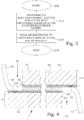
- Fig. 3is a flow diagram of steps of an embodiment of a method for producing an electrochromic device.
- the procedurestarts in step 200.
- an electrochromic layered structureis provided.
- the electrochromic layered structurehas a first substrate sheet, a second substrate sheet, a first electron conducting layer at least partially covering the first substrate sheet, a second electron conducting layer at least partially covering the second substrate sheet, an electrochromic layer at least partially covering the first electron conducting layer, a counter electrode layer at least partially covering the second electron conducting layer, and an electrolyte layer laminated between and at least partially covering the first electrochromic layer and the counter electrode layer.
- the electrochromic layered structurehas a first area in which the electrochromic layer is not covered by the electrolyte layer and/or a second area in which said counter electrode layer is not covered by said electrolyte layer.
- an electrodeis soldered, by ultra sound soldering, to the first electron conducting layer in the first area through the electrochromic layer or to the second electron conducting layer in the second area through the counter electrode layer. The procedure ends in step 299.
- the provision of an electrochromic layer structureis known from prior art.
- the electrochromic layer structuremay be of many different kinds, e.g. it can be based on glass substrates or on polymer substrates.
- the electrochromic layer structuremay also be e.g. laminated into different types of glass pane products.
- the details of how the manufacturing of the actual electrochromic layer structure is madeare in general not particularly important for the present ideas, if not discussed separately further below.
- one possible example of a way to accomplish the provision of the electrochromic layer structureis given here below.
- anyone skilled in the artrealizes that the present ideas are not limited to this particular electrochromic layer structure, but is applicable also to alternative ways of providing the electrochromic layer structure.
- a substrate sheet of PETis provided.
- the PET sheetis coated by ITO by sputtering deposition, thereby providing the substrate with a conducting layer.
- the ITO covered PETis split into two parts. One part is moved through a sputter equipment arranged for sputtering a layer of electrochromic NiO, to be used as counter electrode, on the ITO in a continuous sputtering process.
- the ITO of the other partis moved through the sputter equipment, now arranged for sputtering a layer of electrochromic WO on the ITO in a continuous sputtering process.
- Two entities of covered ITO on PETare thus produced, each one suitable as a half cell in an electrochromic layered structure.
- the half-cell entitiesare provided to a laminator.
- Electrolyteis provided from an electrolyte source into the space between the coated PET substrates and the coated PET substrates and electrolyte are laminated together creating an electrochromic layered structure.
- the laminationcan also be followed by post-treatment, providing e.g. structural supporting features, curing and/or sealing.
- Electrodesare needed to both electron conducting layers in order to provide the current to the electrochromic layer by means of an applied voltage across the electrochromic layer structure.
- the electrodesmay be attached in different ways.
- electrodesare soldered to the respective electron conducting layers below both the electrochromic layer and counter electrode layer, respectively.
- the soldering stepcomprises soldering, by ultra sound soldering, of an electrode to the first electron conducting layer in the first area through the electrochromic layer and soldering, by ultra sound soldering, of an electrode to the second electron conducting layer in the second area through the counter electrode layer.
- At least one of the electrodescomprises a conducting tape.
- the non-covered areas of the electrochromic layered structureare created after the lamination of the main electrochromic layered structure.
- an electrochromic layered structure without the first area and the second areais first provided. Thereafter, the first area and/or the second areas are created.
- a part of the second substrate sheet, the second electron conducting layer, the counter electrode layer and the electrolyteis removed, thereby uncovering the first area and/or a part of the first substrate sheet, the first electron conducting layer, the electrochromic layer and the electrolyte is removed, thereby uncovering the second area.
- the actual removal of the portions of the respective half-cellsmay be performed in different manners.
- the removalis mainly mechanical.
- a cut around a portion in the lateral direction of the half-cellis then provided down through the half-cell down to the electrolyte layer and due to the limited adhesion provided by the electrolyte layer, the cut-out portion of the half-cell is easily removed.
- This cutcan be performed by high-precision control of e.g. a doctor's blade. Any remaining electrolyte is then cleaned off e.g. by wiping with a cloth and/or washing with a solvent.
- a similar cutcan be performed in different manners, e.g. by use of laser ablation or laser cutting.
- different types of etchingcan be performed.
- Fig. 4illustrates a schematic illustration of an embodiment of an electrochromic device 1 manufactured according to the ideas presented above.
- the electrochromic device 1comprises an electrochromic layered structure 10.
- the electrochromic layered structure 10has a first substrate sheet 21 and a second substrate sheet 22.
- a first electron conducting layer 23covers the first substrate sheet 21, at least partially.
- a second electron conducting layer 24covers the second substrate sheet 22, at least partially.
- An electrochromic layer 25covers the first electron conducting layer 23, at least partially.
- a counter electrode layer 26covers the second electron conducting layer 24, at least partially.
- the counter electrode layer 26may in particular embodiments also comprise electrochromic material.
- the first substrate sheet 21, the first electron conducting layer 23 and the electrochromic layer 25together form a first half-cell 11 of the electrochromic structure 10.
- the second substrate sheet 22, the second electron conducting layer 24 and the counter electrode layer 26together form a second half-cell 12 of the electrochromic structure 10.
- An electrolyte layer 30is laminated between the first half-cell 11 and the second half-cell 12. In other words, the electrolyte layer 30 laminated between and at least partially covering the first electrochromic layer 25 and the counter electrode layer 26.
- the electrochromic layered structure 10has a first area 51 in which the electrochromic layer 25 is not covered by the electrolyte layer 30. Likewise, the electrochromic layered structure 10 has a second area 52 in which the counter electrode layer 26 is not covered by the electrolyte layer 30.
- a first electrode 41is soldered to the first electron conducting layer 23 in the first area 51 through, as indicated by the filled cracks 43, the electrochromic layer 25.
- a second electrode 42is soldered to the second electron conducting layer 24 in the second area 52 through, as indicated by the filled cracks 44, the counter electrode layer 26.
- only the first areais present.
- the first electrodecan thereby be attached as above.
- a second electrodeis in such an embodiment attached to the second electron conducting layer in another way.
- only the second areais present.
- the second electrodecan thereby be attached as above.
- a first electrodeis in such an embodiment attached to the first electron conducting layer in another way.
- solders typically used for ultrasonic solderinghave been explored for use in the present processes.
- a contacthas been able to be established through an electrochromic layer with all tested solders.
- an adaptation of the soldering parameters, such as power, frequency etc.had to be performed in order to achieve an acceptable contact.
- Such adaptationsfollow a normal procedure for anyone skilled in the art and are therefore not further discussed.
- As a general trendit seemed that it was easier to find optimum parameters or at least acceptable parameters for solders having good wetting properties.
- the most advantageous choices of solders among the group of tested solderswere solders comprising In, and preferably more than 10% by weight of In.
Landscapes
- Physics & Mathematics (AREA)
- Nonlinear Science (AREA)
- General Physics & Mathematics (AREA)
- Optics & Photonics (AREA)
- Engineering & Computer Science (AREA)
- Mechanical Engineering (AREA)
- Mathematical Physics (AREA)
- Chemical & Material Sciences (AREA)
- Crystallography & Structural Chemistry (AREA)
- Electrochromic Elements, Electrophoresis, Or Variable Reflection Or Absorption Elements (AREA)
Description
- The present invention relates in general to electrochromic devices and in particular to contacting of electrochromic devices.
- Electrochromic devices are today used in widely different applications for enabling control of light transmission. Non-exclusive examples are helmet visors, windows on buildings or automotives, mirrors and goggles. In a typical non-self-erasing electrochromic device, a thin foil of stacked layers is used, incorporating conducting layers, electrochromic layers and an electrolyte layer. In certain embodiments, these layers are provided between two substrate sheets serving as main structural bodies of the electrochromic device. In order to change the transmittance of the device, a voltage is provided between two electron conducting layers. The voltage causes a charging of the electrochromic device, which in turn results in a transmittance change. The level of transmittance is preserved when the voltage is removed.
- An important process step in manufacturing of electrochromic devices is the contacting of the electron conducting layers. Since the electrochromic device generally is very thin, so are the electron conducting layers. Contacting from the sides of the electrochromic device becomes practically impossible or at least very difficult to perform in a more or less automated manner. The typical approach for facilitating contacting is to let one substrate sheet with the associated electron conducting layer protrude outside the other substrate sheet in a direction along the extension of the generally sheet-shaped electrochromic device. The other substrate sheet and the other electron conducting layer are typically protruding at another portion of the device. Contacting of the electron conducting layers can then be performed at these protruding portions.
- Contacting geometries have therefore to be determined in advance. The deposition of the electrochromic layers or counter electrode layers has to be excluded from such areas. Furthermore, during the lamination process, aligning of the substrate has to be performed in order to ensure that the areas intended for contacting do not become covered. Moreover, if the laminated EC laminate is going to be transported before the actual contacting is performed, the exposed areas may be damaged if not being properly protected.
- Also, in different applications, electrochromic devices of varying geometrical shapes may be needed. The final shape may even not be known until just before the actual assembly. In such cases, it can be difficult to provide semi-manufactured electrochromic devices with a correct shape in advance, and it would be beneficial if the final shape of the electrochromic device could be cut out from a larger sheet of an electrochromic layered structure. In such cases, the provision of protruding parts appropriate for contacting becomes even more difficult.
- In the published US patent application
US 2008/0266642 A1 , durable electrooptic devices are disclosed. - In the published international patent application
WO 2008/013501 A1 , contacting of electrochromic devices is disclosed. Holes are provided through the substrates of the electrochromic devices in order to reach electron conducting layers, to which electrodes are soldered. - A general object of the present invention is to facilitate contacting of electrochromic devices. The object is achieved by methods and devices according to the enclosed independent patent claims. Preferred embodiments are defined by the dependent claims. In general words, in a first aspect, a method for producing an electrochromic device comprises providing of an electrochromic layered structure. The electrochromic layered structure has a first substrate sheet, a second substrate sheet, a first electron conducting layer at least partially covering the first substrate sheet, a second electron conducting layer at least partially covering the second substrate sheet, an electrochromic layer at least partially covering the first electron conducting layer, a counter electrode layer at least partially covering the second electron conducting layer, and an electrolyte layer laminated between and at least partially covering he first electrochromic layer and the counter electrode layer. The electrochromic layered structure has a first area in which the electrochromic layer is not covered by the electrolyte layer and/or a second area in which the counter electrode layer is not covered by the electrolyte layer. An electrode is, by use of ultra sound soldering, soldered to the first electron conducting layer in the first area through the electrochromic layer or to the second electron conducting layer in the second area through the counter electrode layer.
- In a second aspect, an electrochromic device comprises an electrochromic layered structure. The electrochromic layered structure has a first substrate sheet, a second substrate sheet, a first electron conducting layer at least partially covering the first substrate sheet, a second electron conducting layer at least partially covering the second substrate sheet, an electrochromic layer at least partially covering the first electron conducting layer, a counter electrode layer at least partially covering the second electron conducting layer and an electrolyte layer laminated between and at least partially covering the first electrochromic layer and the counter electrode layer. The electrochromic layered structure also has a first area in which the electrochromic layer is not covered by the electrolyte layer and/or a second area in which the counter electrode layer is not covered by the electrolyte layer. A first electrode is soldered to the first electron conducting layer in the first area through the electrochromic layer and/or a second electrode is soldered to the second electron conducting layer in the second area through the counter electrode layer.
- One advantage with the present invention is that it enables a more flexible manufacturing. Another advantage with the present invention is that it presents manufacturing well adapted to large-scale production. Other advantages are discussed more in connection with the different embodiments presented further below.
- The invention, together with further objects and advantages thereof, may best be understood by making reference to the following description taken together with the accompanying drawings, in which:
FIG. 1 is an illustration of an ITO surface partially covered by an electrochromic compound;FIG. 2 is an illustration of an ITO surface partially covered by an electrochromic compound with an ultra sound soldering on top;FIG. 3 is a flow diagram of steps of an embodiment of a method for producing an electrochromic device; andFIG. 4 is a schematic illustration of an embodiment of an electrochromic device produced by a method according toFig. 3 .- Throughout the drawings, the same reference numbers are used for similar or corresponding elements.
- One approach to solve the problems of prior art is to first manufacture an electrochromic layered structure without uncovered areas intended for contacting and then in connection with the actual contacting removing a portion of one half-cell and underlying electrolyte to expose the inner surface of the opposite half-cell. By "half-cell" is here understood the part structure composed by a substrate sheet, an electron conducting layer and either an electrochromic layer or a counter electrode layer. The exposed inner surface of the opposite half cell thereby shows a surface covered with either an electrochromic layer or a counter electrode layer. These materials are typically porous oxides, e.g. WO or NiO, and typically poorly conducting.
- The exposed areas of either an electrochromic layer or a counter electrode layer are unsuitable for contacting an electrode by simple mechanical means, such as clamping etc. Also thermal soldering will give poor results since the solder, due to surface tension, only wets the surface of the electrochromic layer or counter electrode layer and the electron conduction using the electrochromic layer or counter electrode layer is too poor.
- However, since the electrochromic layer or counter electrode layer typically is deposited onto the electron conducting layer, e.g. Indium Tin Oxide (ITO), by sputtering techniques and in thin layers, at least in a macroscopic view, removal of the electrochromic layer or counter electrode layer without severely damaging the underlying electron conducting layer becomes very cumbersome. Mechanical removal techniques are in general too rough and chemically based methods are typical unpractical to perform in connection with contacting processes and requires typically additional protective measures to protect the rest of the device.
Fig. 1 illustrates an enlarged portion of anITO surface 100 partially covered with anelectrochromic oxide 106. Thevertical portion 102 of the oxide is in the figure emphasized by an irregular hatching and theITO surface 100 is given a linear hatching in order to make the figure more readable. The oxide is porous and the oxide surface is fractured 104. The oxide is poorly conducting. The same conditions are present at a counter electrode layer.- It has now been discovered that by applying ultrasonic soldering to a material such as electrochromic oxides, an electrical contact can nevertheless be established, i.e. through the poorly conducting oxide. The full understanding of the reasons and processes making this possible is not yet reached. It is experimentally challenging to try to investigate and verify such systems, since the thickness dimension ratios between e.g. the substrate or solder and the electrochromic oxides are very large. However, relatively well supported theories are developed.
- With reference to
Fig. 1 , thecracks 104 in the oxide of the electrochromic or counter electrode layers typically penetrate all the way down through theoxide layer 102 down to the surface of theconductive ITO 100. Typical widths of thecracks 104 are up to 50 nm. However,such cracks 104 are in general too narrow to allow solder from a thermal soldering process to enter due to surface tension effects. At the contrary, during the ultrasonic soldering, the surface tension seems to be reduced. Cavities that are too small to be filled with thermally melted metal due to surface tension reasons, becomes fillable by use of ultrasonic soldering. When the surface tension of the solder material becomes low enough, the capillary forces of the narrow cracks starts to pull the solder through thecracks 104 and pores all the way down to theconductive ITO 100. Probably, the sound waves from the ultrasound soldering equipment also contribute to actively push down the solder into thecracks 104. - An electron conducting path is thereby created through the electrochromic oxide. Each crack or pore is typically very small, but the large numbers of pores and cracks together form an electrical connection having a reasonably low resistance. It is thus possible to contact the ITO layer through the electrochromic oxide by ultrasonic soldering without removing the entire electrochromic oxide.
- The result is schematically illustrated in
Fig. 2 . A layer ofsolder material 108 is provided on top of the electrochromic oxide by means of ultrasonic soldering. Thevertical portion 109 of the solder material is in the figure emphasized by a point hatching. Here the cracks are filled 110 with solder, which thus constitutes a continuous conducting path through theelectrochromic oxide 102. - It is also possible that the ultrasonic waves themselves additionally contribute to an additional cracking of the electrochromic oxide or counter electrode oxide. Such an action will then increase the number of possible conducting channels though the oxides, and thereby increasing the total conductivity. Also the emitted heat and the mechanical handling stresses from the process itself may contribute to additional cracking.
Fig. 3 is a flow diagram of steps of an embodiment of a method for producing an electrochromic device. The procedure starts instep 200. Instep 210, an electrochromic layered structure is provided. The electrochromic layered structure has a first substrate sheet, a second substrate sheet, a first electron conducting layer at least partially covering the first substrate sheet, a second electron conducting layer at least partially covering the second substrate sheet, an electrochromic layer at least partially covering the first electron conducting layer, a counter electrode layer at least partially covering the second electron conducting layer, and an electrolyte layer laminated between and at least partially covering the first electrochromic layer and the counter electrode layer. The provision of an electrochromic layer structure, as such, is known from prior art. The details of how the manufacturing is made are in general not particularly important for the present ideas. Therefore, only parts that are of particular importance for the present disclosed ideas are further discussed. The electrochromic layered structure has a first area in which the electrochromic layer is not covered by the electrolyte layer and/or a second area in which said counter electrode layer is not covered by said electrolyte layer. Instep 220, an electrode is soldered, by ultra sound soldering, to the first electron conducting layer in the first area through the electrochromic layer or to the second electron conducting layer in the second area through the counter electrode layer. The procedure ends instep 299.- The provision of an electrochromic layer structure, as such, is known from prior art. The electrochromic layer structure may be of many different kinds, e.g. it can be based on glass substrates or on polymer substrates. The electrochromic layer structure may also be e.g. laminated into different types of glass pane products. The details of how the manufacturing of the actual electrochromic layer structure is made are in general not particularly important for the present ideas, if not discussed separately further below. However, in order to make the manufacturing information complete, one possible example of a way to accomplish the provision of the electrochromic layer structure is given here below. However, anyone skilled in the art realizes that the present ideas are not limited to this particular electrochromic layer structure, but is applicable also to alternative ways of providing the electrochromic layer structure.
- A substrate sheet of PET is provided. The PET sheet is coated by ITO by sputtering deposition, thereby providing the substrate with a conducting layer. The ITO covered PET is split into two parts. One part is moved through a sputter equipment arranged for sputtering a layer of electrochromic NiO, to be used as counter electrode, on the ITO in a continuous sputtering process. The ITO of the other part is moved through the sputter equipment, now arranged for sputtering a layer of electrochromic WO on the ITO in a continuous sputtering process. These two sputtering processes can also be performed simultaneously in two parallel process lines. Two entities of covered ITO on PET are thus produced, each one suitable as a half cell in an electrochromic layered structure. The half-cell entities are provided to a laminator. Electrolyte is provided from an electrolyte source into the space between the coated PET substrates and the coated PET substrates and electrolyte are laminated together creating an electrochromic layered structure. The lamination can also be followed by post-treatment, providing e.g. structural supporting features, curing and/or sealing.
- Electrodes are needed to both electron conducting layers in order to provide the current to the electrochromic layer by means of an applied voltage across the electrochromic layer structure. The electrodes may be attached in different ways. However, in a preferred embodiment, electrodes are soldered to the respective electron conducting layers below both the electrochromic layer and counter electrode layer, respectively. In other words, the soldering step comprises soldering, by ultra sound soldering, of an electrode to the first electron conducting layer in the first area through the electrochromic layer and soldering, by ultra sound soldering, of an electrode to the second electron conducting layer in the second area through the counter electrode layer.
- In a preferred embodiment, at least one of the electrodes comprises a conducting tape.
- In one embodiment, the non-covered areas of the electrochromic layered structure are created after the lamination of the main electrochromic layered structure. In other words, an electrochromic layered structure without the first area and the second area is first provided. Thereafter, the first area and/or the second areas are created. In other words, a part of the second substrate sheet, the second electron conducting layer, the counter electrode layer and the electrolyte is removed, thereby uncovering the first area and/or a part of the first substrate sheet, the first electron conducting layer, the electrochromic layer and the electrolyte is removed, thereby uncovering the second area.
- The actual removal of the portions of the respective half-cells may be performed in different manners. In one embodiment, the removal is mainly mechanical. A cut around a portion in the lateral direction of the half-cell, is then provided down through the half-cell down to the electrolyte layer and due to the limited adhesion provided by the electrolyte layer, the cut-out portion of the half-cell is easily removed. This cut can be performed by high-precision control of e.g. a doctor's blade. Any remaining electrolyte is then cleaned off e.g. by wiping with a cloth and/or washing with a solvent. In an alternative embodiment, a similar cut can be performed in different manners, e.g. by use of laser ablation or laser cutting. In further alternative embodiments, different types of etching can be performed.
Fig. 4 illustrates a schematic illustration of an embodiment of anelectrochromic device 1 manufactured according to the ideas presented above. Theelectrochromic device 1 comprises an electrochromiclayered structure 10. The electrochromiclayered structure 10 has afirst substrate sheet 21 and asecond substrate sheet 22. A firstelectron conducting layer 23 covers thefirst substrate sheet 21, at least partially. A secondelectron conducting layer 24 covers thesecond substrate sheet 22, at least partially.- An
electrochromic layer 25 covers the firstelectron conducting layer 23, at least partially. Acounter electrode layer 26 covers the secondelectron conducting layer 24, at least partially. Thecounter electrode layer 26 may in particular embodiments also comprise electrochromic material. Thefirst substrate sheet 21, the firstelectron conducting layer 23 and theelectrochromic layer 25 together form a first half-cell 11 of theelectrochromic structure 10. Thesecond substrate sheet 22, the secondelectron conducting layer 24 and thecounter electrode layer 26 together form a second half-cell 12 of theelectrochromic structure 10. Anelectrolyte layer 30 is laminated between the first half-cell 11 and the second half-cell 12. In other words, theelectrolyte layer 30 laminated between and at least partially covering thefirst electrochromic layer 25 and thecounter electrode layer 26. - In the embodiment of
Fig. 4 , the electrochromiclayered structure 10 has afirst area 51 in which theelectrochromic layer 25 is not covered by theelectrolyte layer 30. Likewise, the electrochromiclayered structure 10 has asecond area 52 in which thecounter electrode layer 26 is not covered by theelectrolyte layer 30. Afirst electrode 41 is soldered to the firstelectron conducting layer 23 in thefirst area 51 through, as indicated by the filled cracks 43, theelectrochromic layer 25. Asecond electrode 42 is soldered to the secondelectron conducting layer 24 in thesecond area 52 through, as indicated by the filled cracks 44, thecounter electrode layer 26. - In one alternative embodiment, only the first area is present. The first electrode can thereby be attached as above. A second electrode is in such an embodiment attached to the second electron conducting layer in another way. In another embodiment, only the second area is present. The second electrode can thereby be attached as above. A first electrode is in such an embodiment attached to the first electron conducting layer in another way.
- A number of different solders typically used for ultrasonic soldering have been explored for use in the present processes. A contact has been able to be established through an electrochromic layer with all tested solders. However, in some cases, an adaptation of the soldering parameters, such as power, frequency etc. had to be performed in order to achieve an acceptable contact. Such adaptations follow a normal procedure for anyone skilled in the art and are therefore not further discussed. As a general trend, it seemed that it was easier to find optimum parameters or at least acceptable parameters for solders having good wetting properties. The most advantageous choices of solders among the group of tested solders were solders comprising In, and preferably more than 10% by weight of In.
- The embodiments described above are to be understood as a few illustrative examples of the present invention. It will be understood by those skilled in the art that various modifications, combinations and changes may be made to the embodiments without departing from the scope of the present invention. In particular, different part solutions in the different embodiments can be combined in other configurations, where technically possible. The scope of the present invention is, however, defined by the appended claims.
Claims (11)
- A method for producing an electrochromic device, comprising the steps of:providing (210) an electrochromic layered structure, having a first substrate sheet, a second substrate sheet, a first electron conducting layer at least partially covering said first substrate sheet, a second electron conducting layer at least partially covering said second substrate sheet, an electrochromic layer at least partially covering said first electron conducting layer, a counter electrode layer at least partially covering said second electron conducting layer, and an electrolyte layer laminated between and at least partially covering said first electrochromic layer and said counter electrode layer;said electrochromic layered structure having at least one of:- a first area in which said electrochromic layer is not covered by said electrolyte layer; and- a second area in which said counter electrode layer is not covered by said electrolyte layer,characterized byat least one of:- soldering (220), by ultra sound soldering, an electrode to said first electron conducting layer in said first area through said electrochromic layer; and- soldering (220), by ultra sound soldering, an electrode to said second electron conducting layer in said second area through said counter electrode layer.
- The method according to claim 1,characterized in that said soldering (220) comprises soldering, by ultra sound soldering, of an electrode to said first electron conducting layer in said first area through said electrochromic layer and soldering, by ultra sound soldering, of an electrode to said second electron conducting layer in said second area through said counter electrode layer.
- The method according to claim 1 or 2,characterized in that said soldering (220) is performed using a solder comprising In.
- The method according to claim 3,characterized in that said solder comprises In in an amount exceeding 10% by weight.
- The method according to any of the claims 1 to 4,characterized in that at least one of said electrodes comprises a conducting tape.
- The method according to any of the claims 1 to 5,characterized in that said step of providing (210) an electrochromic layered structure, comprises:
providing of an electrochromic layered structure without said first area and said second area; and at least one of:removing a part of said second substrate sheet, said second electron conducting layer, said counter electrode layer and said electrolyte, thereby uncovering said first area; andremoving a part of said first substrate sheet, said first electron conducting layer, said electrochromic layer and said electrolyte, thereby uncovering said second area. - An electrochromic device (1), comprising:an electrochromic layered structure (10), having:a first substrate sheet (21);a second substrate sheet (22);a first electron conducting layer (23) at least partially covering said first substrate sheet (21);a second electron conducting layer (24) at least partially covering said second substrate sheet (22);an electrochromic layer (25) at least partially covering said first electron conducting layer (23);a counter electrode layer (26) at least partially covering said second electron conducting layer (24); andan electrolyte layer (30) laminated between and at least partially covering said first electrochromic layer (25) and said counter electrode layer (26);said electrochromic layered structure (10) having at least one of:- a first area (51) in which said electrochromic layer (25) is not covered by said electrolyte layer (30); and- a second area (52) in which said counter electrode layer (26) is not covered by said electrolyte layer (30),characterized in that at least one of:- a first electrode (41) being soldered to said first electron conducting layer (23) in said first area (51) through said electrochromic layer (25); and- a second electrode (42) being soldered to said second electron conducting layer (24) in said second area (52) through said counter electrode layer (26).
- The electrochromic device according to claim 7,characterized in that a first electrode (41) being soldered to said first electron conducting layer (23) in said first area (51) through said electrochromic layer (25) and a second electrode (42) being soldered to said second electron conducting layer (24) in said second area (52) through said counter electrode layer (26).
- The electrochromic device according to claim 7 or 8,characterized in that at least one of said first and second electrodes (41, 42) is soldered by a solder comprising In.
- The electrochromic device according to claim 9,characterized in that said solder comprises In in an amount exceeding 10% by weight.
- The electrochromic device according to any of the claims 7 to 10,characterized in that at least one of said first electrode (41) and said second electrode (42) comprises a conducting tape.
Applications Claiming Priority (2)
| Application Number | Priority Date | Filing Date | Title |
|---|---|---|---|
| SE1350916 | 2013-07-29 | ||
| PCT/SE2014/050902WO2015016764A1 (en) | 2013-07-29 | 2014-07-23 | Contacting of electrochromic devices |
Publications (3)
| Publication Number | Publication Date |
|---|---|
| EP3027346A1 EP3027346A1 (en) | 2016-06-08 |
| EP3027346A4 EP3027346A4 (en) | 2017-04-12 |
| EP3027346B1true EP3027346B1 (en) | 2018-06-20 |
Family
ID=52432162
Family Applications (1)
| Application Number | Title | Priority Date | Filing Date |
|---|---|---|---|
| EP14832244.9AActiveEP3027346B1 (en) | 2013-07-29 | 2014-07-23 | Contacting of electrochromic devices |
Country Status (6)
| Country | Link |
|---|---|
| US (1) | US9778531B2 (en) |
| EP (1) | EP3027346B1 (en) |
| JP (1) | JP6408577B2 (en) |
| CN (1) | CN105358281B (en) |
| ES (1) | ES2687597T3 (en) |
| WO (1) | WO2015016764A1 (en) |
Families Citing this family (15)
| Publication number | Priority date | Publication date | Assignee | Title |
|---|---|---|---|---|
| KR102654925B1 (en) | 2016-06-21 | 2024-04-05 | 삼성디스플레이 주식회사 | Display apparatus and manufacturing method of the same |
| WO2018195458A1 (en) | 2017-04-20 | 2018-10-25 | Cardinal Ig Company | High performance privacy glazing structures |
| WO2019014613A1 (en)* | 2017-07-13 | 2019-01-17 | Cardinal Ig Company | Electrical connection configurations for privacy glazing structures |
| EP3707555B1 (en) | 2017-11-06 | 2025-05-07 | Cardinal Ig Company | Privacy glazing system with discrete electrical driver |
| MX2020011871A (en) | 2018-05-09 | 2021-01-20 | Cardinal Ig Co | Electrically controllable privacy glazing with energy recapturing driver. |
| CN112654919B (en) | 2018-08-17 | 2024-05-28 | 卡迪纳尔Ig公司 | Privacy glazing structure with asymmetric pane offset for electrical connection configuration |
| US11474385B1 (en) | 2018-12-02 | 2022-10-18 | Cardinal Ig Company | Electrically controllable privacy glazing with ultralow power consumption comprising a liquid crystal material having a light transmittance that varies in response to application of an electric field |
| WO2020163836A1 (en) | 2019-02-08 | 2020-08-13 | Cardinal Ig Company | Low power driver for privacy glazing |
| US11175523B2 (en) | 2019-04-29 | 2021-11-16 | Cardinal Ig Company | Staggered driving electrical control of a plurality of electrically controllable privacy glazing structures |
| KR102809744B1 (en) | 2019-04-29 | 2025-05-16 | 카디날 아이지 컴퍼니 | Leakage current detection and control for one or more electrically controllable privacy glass structures |
| MX2021013259A (en) | 2019-04-29 | 2022-01-06 | Cardinal Ig Co | SYSTEMS AND METHODS FOR OPERATING ONE OR MORE GLAZING STRUCTURES WITH ELECTRICALLY CONTROLLABLE PRIVACY. |
| SE543836C2 (en)* | 2019-12-20 | 2021-08-10 | Chromogenics Ab | Contact protecting edge structure on glass laminates |
| CN111594023A (en)* | 2020-06-03 | 2020-08-28 | 江苏铁锚玻璃股份有限公司 | Light modulation glass assembly and light modulation window |
| US20220219254A1 (en)* | 2021-01-13 | 2022-07-14 | Carlex Glass America, Llc | Method of connection to a conductive material |
| CN115793340B (en)* | 2022-12-29 | 2024-06-28 | 光羿智能科技(苏州)有限公司 | Electrochromic device, electrochromic glass and rearview mirror |
Family Cites Families (20)
| Publication number | Priority date | Publication date | Assignee | Title |
|---|---|---|---|---|
| DE3211651A1 (en)* | 1982-03-30 | 1983-10-06 | Bosch Gmbh Robert | ELECTROCHROME DISPLAY DEVICE |
| JPS6214118A (en)* | 1985-07-12 | 1987-01-22 | Canon Inc | electrochromic device |
| US4851308A (en)* | 1988-01-19 | 1989-07-25 | Chronar Corp. | Solid-state energy storage cell wherein the electrolyte comprises an organic support and an inorganic salt |
| US5668663A (en) | 1994-05-05 | 1997-09-16 | Donnelly Corporation | Electrochromic mirrors and devices |
| JPH11500838A (en)* | 1995-12-15 | 1999-01-19 | フィリップス エレクトロニクス ネムローゼ フェンノートシャップ | Electrochromic devices and display devices containing such devices |
| US5724175A (en)* | 1997-01-02 | 1998-03-03 | Optical Coating Laboratory, Inc. | Electrochromic device manufacturing process |
| US5886687A (en)* | 1997-02-20 | 1999-03-23 | Gibson; William A. | Touch panel system utilizing capacitively-coupled electrodes |
| US7255451B2 (en) | 2002-09-20 | 2007-08-14 | Donnelly Corporation | Electro-optic mirror cell |
| US7450292B1 (en)* | 2003-06-20 | 2008-11-11 | Los Alamos National Security, Llc | Durable electrooptic devices comprising ionic liquids |
| CN100386691C (en)* | 2002-06-21 | 2008-05-07 | 洛斯阿拉莫斯国家安全股份有限公司 | Electrooptical device containing ionic liquid, electrooptical automobile mirror and electrolyte used for electrooptical device and electrooptical automobile mirror |
| JP5026032B2 (en)* | 2005-12-28 | 2012-09-12 | シチズンファインテックミヨタ株式会社 | Liquid crystal display device and manufacturing method thereof |
| ES2365072T3 (en)* | 2006-07-28 | 2011-09-21 | Chromogenics Ab | MANUFACTURE OF ELECTROCROMIC DEVICES. |
| DE602007012890D1 (en)* | 2006-07-28 | 2011-04-14 | Chromogenics Sweden Ab | CONTACTING ELECTROCHROMICAL ARRANGEMENTS |
| EP2049942B1 (en)* | 2006-07-28 | 2011-01-19 | Chromogenics Sweden AB | Manufacturing of curved electrochromic devices |
| KR20100017542A (en) | 2007-06-01 | 2010-02-16 | 크로모제닉스 에이비 | Control of Electrochromic Devices |
| JP2009094467A (en)* | 2007-09-18 | 2009-04-30 | Fujifilm Corp | Image display device, moire suppression film, optical filter, plasma display filter, image display panel |
| FR2942665B1 (en) | 2009-03-02 | 2011-11-04 | Saint Gobain | ELECTROCOMMANDABLE DEVICE HOMOGENEOUS COLORING / DECOLORIZING ON THE WHOLE SURFACE |
| US9664974B2 (en) | 2009-03-31 | 2017-05-30 | View, Inc. | Fabrication of low defectivity electrochromic devices |
| FR2944610B1 (en)* | 2009-04-16 | 2011-06-24 | Saint Gobain | ELECTROCHROME DEVICE HAVING CONTROLLED TRANSPARENCY |
| CN103502883B (en) | 2011-04-06 | 2016-02-17 | 显色公司 | Electrochromic device |
- 2014
- 2014-07-23ESES14832244.9Tpatent/ES2687597T3/enactiveActive
- 2014-07-23EPEP14832244.9Apatent/EP3027346B1/enactiveActive
- 2014-07-23CNCN201480038335.0Apatent/CN105358281B/enactiveActive
- 2014-07-23WOPCT/SE2014/050902patent/WO2015016764A1/enactiveApplication Filing
- 2014-07-23USUS14/906,398patent/US9778531B2/enactiveActive
- 2014-07-23JPJP2016531583Apatent/JP6408577B2/enactiveActive
Non-Patent Citations (1)
| Title |
|---|
| None* |
Also Published As
| Publication number | Publication date |
|---|---|
| JP2016534388A (en) | 2016-11-04 |
| US9778531B2 (en) | 2017-10-03 |
| CN105358281A (en) | 2016-02-24 |
| ES2687597T3 (en) | 2018-10-26 |
| EP3027346A4 (en) | 2017-04-12 |
| EP3027346A1 (en) | 2016-06-08 |
| WO2015016764A1 (en) | 2015-02-05 |
| CN105358281B (en) | 2018-08-07 |
| US20160161818A1 (en) | 2016-06-09 |
| JP6408577B2 (en) | 2018-10-17 |
Similar Documents
| Publication | Publication Date | Title |
|---|---|---|
| EP3027346B1 (en) | Contacting of electrochromic devices | |
| US20240019749A1 (en) | Non-light-emitting variable transmission device and a method of forming the same | |
| KR102095605B1 (en) | Thin-film devices and fabrication | |
| EP2593832B1 (en) | Method of manufacturing an electrochromic device | |
| US11994781B2 (en) | Electrochromic structure and method of separating electrochromic structure | |
| US10012887B2 (en) | Electrochromic devices and manufacturing methods thereof | |
| TWI691772B (en) | Thin-film devices and fabrication | |
| CN110914055B (en) | Multilayer films with electrically switchable optical properties and improved electrical contacts | |
| TW202102919A (en) | Method and system for fabricating electrochromic devices | |
| US10509291B2 (en) | Electrical device including a substrate and a transparent conductive layer and a process of forming the same | |
| WO2017169243A1 (en) | Solid state ec mirror and manufacturing method therefor | |
| CN116719433A (en) | Nano silver touch sensor and processing method and application thereof | |
| JP2010250956A (en) | Method for forming catalyst layer of fuel cell |
Legal Events
| Date | Code | Title | Description |
|---|---|---|---|
| PUAI | Public reference made under article 153(3) epc to a published international application that has entered the european phase | Free format text:ORIGINAL CODE: 0009012 | |
| 17P | Request for examination filed | Effective date:20160229 | |
| AK | Designated contracting states | Kind code of ref document:A1 Designated state(s):AL AT BE BG CH CY CZ DE DK EE ES FI FR GB GR HR HU IE IS IT LI LT LU LV MC MK MT NL NO PL PT RO RS SE SI SK SM TR | |
| AX | Request for extension of the european patent | Extension state:BA ME | |
| DAX | Request for extension of the european patent (deleted) | ||
| A4 | Supplementary search report drawn up and despatched | Effective date:20170313 | |
| RIC1 | Information provided on ipc code assigned before grant | Ipc:G02F 1/155 20060101ALI20170307BHEP Ipc:G02F 1/1345 20060101ALN20170307BHEP Ipc:G02F 1/1343 20060101ALN20170307BHEP Ipc:G02F 1/153 20060101ALI20170307BHEP Ipc:B23K 1/06 20060101AFI20170307BHEP | |
| RAP1 | Party data changed (applicant data changed or rights of an application transferred) | Owner name:CHROMOGENICS AB | |
| 17Q | First examination report despatched | Effective date:20170818 | |
| RIC1 | Information provided on ipc code assigned before grant | Ipc:B23K 1/06 20060101AFI20180131BHEP Ipc:G02F 1/155 20060101ALI20180131BHEP Ipc:G02F 1/1345 20060101ALN20180131BHEP Ipc:G02F 1/153 20060101ALI20180131BHEP Ipc:G02F 1/1343 20060101ALN20180131BHEP | |
| GRAP | Despatch of communication of intention to grant a patent | Free format text:ORIGINAL CODE: EPIDOSNIGR1 | |
| RIC1 | Information provided on ipc code assigned before grant | Ipc:B23K 1/06 20060101AFI20180221BHEP Ipc:G02F 1/1343 20060101ALN20180221BHEP Ipc:G02F 1/1345 20060101ALN20180221BHEP Ipc:G02F 1/153 20060101ALI20180221BHEP Ipc:G02F 1/155 20060101ALI20180221BHEP | |
| RIC1 | Information provided on ipc code assigned before grant | Ipc:G02F 1/153 20060101ALI20180308BHEP Ipc:G02F 1/155 20060101ALI20180308BHEP Ipc:G02F 1/1343 20060101ALN20180308BHEP Ipc:G02F 1/1345 20060101ALN20180308BHEP Ipc:B23K 1/06 20060101AFI20180308BHEP | |
| INTG | Intention to grant announced | Effective date:20180323 | |
| GRAS | Grant fee paid | Free format text:ORIGINAL CODE: EPIDOSNIGR3 | |
| GRAA | (expected) grant | Free format text:ORIGINAL CODE: 0009210 | |
| AK | Designated contracting states | Kind code of ref document:B1 Designated state(s):AL AT BE BG CH CY CZ DE DK EE ES FI FR GB GR HR HU IE IS IT LI LT LU LV MC MK MT NL NO PL PT RO RS SE SI SK SM TR | |
| REG | Reference to a national code | Ref country code:GB Ref legal event code:FG4D | |
| REG | Reference to a national code | Ref country code:IE Ref legal event code:FG4D | |
| REG | Reference to a national code | Ref country code:AT Ref legal event code:REF Ref document number:1010224 Country of ref document:AT Kind code of ref document:T Effective date:20180715 | |
| REG | Reference to a national code | Ref country code:DE Ref legal event code:R096 Ref document number:602014027374 Country of ref document:DE | |
| REG | Reference to a national code | Ref country code:FR Ref legal event code:PLFP Year of fee payment:5 | |
| REG | Reference to a national code | Ref country code:NL Ref legal event code:MP Effective date:20180620 | |
| REG | Reference to a national code | Ref country code:ES Ref legal event code:FG2A Ref document number:2687597 Country of ref document:ES Kind code of ref document:T3 Effective date:20181026 | |
| PG25 | Lapsed in a contracting state [announced via postgrant information from national office to epo] | Ref country code:SE Free format text:LAPSE BECAUSE OF FAILURE TO SUBMIT A TRANSLATION OF THE DESCRIPTION OR TO PAY THE FEE WITHIN THE PRESCRIBED TIME-LIMIT Effective date:20180620 Ref country code:LT Free format text:LAPSE BECAUSE OF FAILURE TO SUBMIT A TRANSLATION OF THE DESCRIPTION OR TO PAY THE FEE WITHIN THE PRESCRIBED TIME-LIMIT Effective date:20180620 Ref country code:BG Free format text:LAPSE BECAUSE OF FAILURE TO SUBMIT A TRANSLATION OF THE DESCRIPTION OR TO PAY THE FEE WITHIN THE PRESCRIBED TIME-LIMIT Effective date:20180920 Ref country code:FI Free format text:LAPSE BECAUSE OF FAILURE TO SUBMIT A TRANSLATION OF THE DESCRIPTION OR TO PAY THE FEE WITHIN THE PRESCRIBED TIME-LIMIT Effective date:20180620 Ref country code:NO Free format text:LAPSE BECAUSE OF FAILURE TO SUBMIT A TRANSLATION OF THE DESCRIPTION OR TO PAY THE FEE WITHIN THE PRESCRIBED TIME-LIMIT Effective date:20180920 | |
| REG | Reference to a national code | Ref country code:LT Ref legal event code:MG4D | |
| PG25 | Lapsed in a contracting state [announced via postgrant information from national office to epo] | Ref country code:GR Free format text:LAPSE BECAUSE OF FAILURE TO SUBMIT A TRANSLATION OF THE DESCRIPTION OR TO PAY THE FEE WITHIN THE PRESCRIBED TIME-LIMIT Effective date:20180921 Ref country code:RS Free format text:LAPSE BECAUSE OF FAILURE TO SUBMIT A TRANSLATION OF THE DESCRIPTION OR TO PAY THE FEE WITHIN THE PRESCRIBED TIME-LIMIT Effective date:20180620 Ref country code:LV Free format text:LAPSE BECAUSE OF FAILURE TO SUBMIT A TRANSLATION OF THE DESCRIPTION OR TO PAY THE FEE WITHIN THE PRESCRIBED TIME-LIMIT Effective date:20180620 Ref country code:HR Free format text:LAPSE BECAUSE OF FAILURE TO SUBMIT A TRANSLATION OF THE DESCRIPTION OR TO PAY THE FEE WITHIN THE PRESCRIBED TIME-LIMIT Effective date:20180620 | |
| REG | Reference to a national code | Ref country code:AT Ref legal event code:MK05 Ref document number:1010224 Country of ref document:AT Kind code of ref document:T Effective date:20180620 | |
| PG25 | Lapsed in a contracting state [announced via postgrant information from national office to epo] | Ref country code:NL Free format text:LAPSE BECAUSE OF FAILURE TO SUBMIT A TRANSLATION OF THE DESCRIPTION OR TO PAY THE FEE WITHIN THE PRESCRIBED TIME-LIMIT Effective date:20180620 | |
| PG25 | Lapsed in a contracting state [announced via postgrant information from national office to epo] | Ref country code:SK Free format text:LAPSE BECAUSE OF FAILURE TO SUBMIT A TRANSLATION OF THE DESCRIPTION OR TO PAY THE FEE WITHIN THE PRESCRIBED TIME-LIMIT Effective date:20180620 Ref country code:EE Free format text:LAPSE BECAUSE OF FAILURE TO SUBMIT A TRANSLATION OF THE DESCRIPTION OR TO PAY THE FEE WITHIN THE PRESCRIBED TIME-LIMIT Effective date:20180620 Ref country code:IS Free format text:LAPSE BECAUSE OF FAILURE TO SUBMIT A TRANSLATION OF THE DESCRIPTION OR TO PAY THE FEE WITHIN THE PRESCRIBED TIME-LIMIT Effective date:20181020 Ref country code:PL Free format text:LAPSE BECAUSE OF FAILURE TO SUBMIT A TRANSLATION OF THE DESCRIPTION OR TO PAY THE FEE WITHIN THE PRESCRIBED TIME-LIMIT Effective date:20180620 Ref country code:AT Free format text:LAPSE BECAUSE OF FAILURE TO SUBMIT A TRANSLATION OF THE DESCRIPTION OR TO PAY THE FEE WITHIN THE PRESCRIBED TIME-LIMIT Effective date:20180620 Ref country code:CZ Free format text:LAPSE BECAUSE OF FAILURE TO SUBMIT A TRANSLATION OF THE DESCRIPTION OR TO PAY THE FEE WITHIN THE PRESCRIBED TIME-LIMIT Effective date:20180620 Ref country code:RO Free format text:LAPSE BECAUSE OF FAILURE TO SUBMIT A TRANSLATION OF THE DESCRIPTION OR TO PAY THE FEE WITHIN THE PRESCRIBED TIME-LIMIT Effective date:20180620 | |
| PG25 | Lapsed in a contracting state [announced via postgrant information from national office to epo] | Ref country code:SM Free format text:LAPSE BECAUSE OF FAILURE TO SUBMIT A TRANSLATION OF THE DESCRIPTION OR TO PAY THE FEE WITHIN THE PRESCRIBED TIME-LIMIT Effective date:20180620 | |
| REG | Reference to a national code | Ref country code:CH Ref legal event code:PL | |
| REG | Reference to a national code | Ref country code:DE Ref legal event code:R097 Ref document number:602014027374 Country of ref document:DE | |
| PG25 | Lapsed in a contracting state [announced via postgrant information from national office to epo] | Ref country code:MC Free format text:LAPSE BECAUSE OF FAILURE TO SUBMIT A TRANSLATION OF THE DESCRIPTION OR TO PAY THE FEE WITHIN THE PRESCRIBED TIME-LIMIT Effective date:20180620 Ref country code:LU Free format text:LAPSE BECAUSE OF NON-PAYMENT OF DUE FEES Effective date:20180723 | |
| REG | Reference to a national code | Ref country code:BE Ref legal event code:MM Effective date:20180731 | |
| REG | Reference to a national code | Ref country code:IE Ref legal event code:MM4A | |
| PLBE | No opposition filed within time limit | Free format text:ORIGINAL CODE: 0009261 | |
| STAA | Information on the status of an ep patent application or granted ep patent | Free format text:STATUS: NO OPPOSITION FILED WITHIN TIME LIMIT | |
| PG25 | Lapsed in a contracting state [announced via postgrant information from national office to epo] | Ref country code:CH Free format text:LAPSE BECAUSE OF NON-PAYMENT OF DUE FEES Effective date:20180731 Ref country code:IE Free format text:LAPSE BECAUSE OF NON-PAYMENT OF DUE FEES Effective date:20180723 Ref country code:LI Free format text:LAPSE BECAUSE OF NON-PAYMENT OF DUE FEES Effective date:20180731 | |
| 26N | No opposition filed | Effective date:20190321 | |
| PG25 | Lapsed in a contracting state [announced via postgrant information from national office to epo] | Ref country code:DK Free format text:LAPSE BECAUSE OF FAILURE TO SUBMIT A TRANSLATION OF THE DESCRIPTION OR TO PAY THE FEE WITHIN THE PRESCRIBED TIME-LIMIT Effective date:20180620 Ref country code:BE Free format text:LAPSE BECAUSE OF NON-PAYMENT OF DUE FEES Effective date:20180731 | |
| PG25 | Lapsed in a contracting state [announced via postgrant information from national office to epo] | Ref country code:SI Free format text:LAPSE BECAUSE OF FAILURE TO SUBMIT A TRANSLATION OF THE DESCRIPTION OR TO PAY THE FEE WITHIN THE PRESCRIBED TIME-LIMIT Effective date:20180620 | |
| PG25 | Lapsed in a contracting state [announced via postgrant information from national office to epo] | Ref country code:AL Free format text:LAPSE BECAUSE OF FAILURE TO SUBMIT A TRANSLATION OF THE DESCRIPTION OR TO PAY THE FEE WITHIN THE PRESCRIBED TIME-LIMIT Effective date:20180620 | |
| PG25 | Lapsed in a contracting state [announced via postgrant information from national office to epo] | Ref country code:MT Free format text:LAPSE BECAUSE OF NON-PAYMENT OF DUE FEES Effective date:20180723 | |
| PG25 | Lapsed in a contracting state [announced via postgrant information from national office to epo] | Ref country code:PT Free format text:LAPSE BECAUSE OF FAILURE TO SUBMIT A TRANSLATION OF THE DESCRIPTION OR TO PAY THE FEE WITHIN THE PRESCRIBED TIME-LIMIT Effective date:20180620 | |
| PG25 | Lapsed in a contracting state [announced via postgrant information from national office to epo] | Ref country code:CY Free format text:LAPSE BECAUSE OF FAILURE TO SUBMIT A TRANSLATION OF THE DESCRIPTION OR TO PAY THE FEE WITHIN THE PRESCRIBED TIME-LIMIT Effective date:20180620 Ref country code:HU Free format text:LAPSE BECAUSE OF FAILURE TO SUBMIT A TRANSLATION OF THE DESCRIPTION OR TO PAY THE FEE WITHIN THE PRESCRIBED TIME-LIMIT; INVALID AB INITIO Effective date:20140723 Ref country code:MK Free format text:LAPSE BECAUSE OF NON-PAYMENT OF DUE FEES Effective date:20180620 | |
| PGFP | Annual fee paid to national office [announced via postgrant information from national office to epo] | Ref country code:GB Payment date:20240612 Year of fee payment:11 | |
| PGFP | Annual fee paid to national office [announced via postgrant information from national office to epo] | Ref country code:IT Payment date:20240610 Year of fee payment:11 Ref country code:FR Payment date:20240612 Year of fee payment:11 | |
| PGFP | Annual fee paid to national office [announced via postgrant information from national office to epo] | Ref country code:TR Payment date:20240613 Year of fee payment:11 | |
| PGFP | Annual fee paid to national office [announced via postgrant information from national office to epo] | Ref country code:DE Payment date:20240610 Year of fee payment:11 | |
| PGFP | Annual fee paid to national office [announced via postgrant information from national office to epo] | Ref country code:ES Payment date:20240912 Year of fee payment:11 |