EP3020092B1 - Radio frequency harvester assembly - Google Patents
Radio frequency harvester assemblyDownload PDFInfo
- Publication number
- EP3020092B1 EP3020092B1EP14742131.7AEP14742131AEP3020092B1EP 3020092 B1EP3020092 B1EP 3020092B1EP 14742131 AEP14742131 AEP 14742131AEP 3020092 B1EP3020092 B1EP 3020092B1
- Authority
- EP
- European Patent Office
- Prior art keywords
- spiral
- antenna
- antennae
- layer
- balun
- Prior art date
- Legal status (The legal status is an assumption and is not a legal conclusion. Google has not performed a legal analysis and makes no representation as to the accuracy of the status listed.)
- Active
Links
Images


Classifications
- H—ELECTRICITY
- H02—GENERATION; CONVERSION OR DISTRIBUTION OF ELECTRIC POWER
- H02J—CIRCUIT ARRANGEMENTS OR SYSTEMS FOR SUPPLYING OR DISTRIBUTING ELECTRIC POWER; SYSTEMS FOR STORING ELECTRIC ENERGY
- H02J50/00—Circuit arrangements or systems for wireless supply or distribution of electric power
- H02J50/20—Circuit arrangements or systems for wireless supply or distribution of electric power using microwaves or radio frequency waves
- H02J50/27—Circuit arrangements or systems for wireless supply or distribution of electric power using microwaves or radio frequency waves characterised by the type of receiving antennas, e.g. rectennas
- H—ELECTRICITY
- H01—ELECTRIC ELEMENTS
- H01Q—ANTENNAS, i.e. RADIO AERIALS
- H01Q1/00—Details of, or arrangements associated with, antennas
- H01Q1/12—Supports; Mounting means
- H01Q1/22—Supports; Mounting means by structural association with other equipment or articles
- H01Q1/24—Supports; Mounting means by structural association with other equipment or articles with receiving set
- H01Q1/248—Supports; Mounting means by structural association with other equipment or articles with receiving set provided with an AC/DC converting device, e.g. rectennas
- H—ELECTRICITY
- H01—ELECTRIC ELEMENTS
- H01Q—ANTENNAS, i.e. RADIO AERIALS
- H01Q1/00—Details of, or arrangements associated with, antennas
- H01Q1/36—Structural form of radiating elements, e.g. cone, spiral, umbrella; Particular materials used therewith
- H—ELECTRICITY
- H01—ELECTRIC ELEMENTS
- H01Q—ANTENNAS, i.e. RADIO AERIALS
- H01Q1/00—Details of, or arrangements associated with, antennas
- H01Q1/36—Structural form of radiating elements, e.g. cone, spiral, umbrella; Particular materials used therewith
- H01Q1/38—Structural form of radiating elements, e.g. cone, spiral, umbrella; Particular materials used therewith formed by a conductive layer on an insulating support
- H—ELECTRICITY
- H01—ELECTRIC ELEMENTS
- H01Q—ANTENNAS, i.e. RADIO AERIALS
- H01Q21/00—Antenna arrays or systems
- H01Q21/06—Arrays of individually energised antenna units similarly polarised and spaced apart
- H—ELECTRICITY
- H01—ELECTRIC ELEMENTS
- H01Q—ANTENNAS, i.e. RADIO AERIALS
- H01Q21/00—Antenna arrays or systems
- H01Q21/06—Arrays of individually energised antenna units similarly polarised and spaced apart
- H01Q21/061—Two dimensional planar arrays
- H—ELECTRICITY
- H01—ELECTRIC ELEMENTS
- H01Q—ANTENNAS, i.e. RADIO AERIALS
- H01Q21/00—Antenna arrays or systems
- H01Q21/24—Combinations of antenna units polarised in different directions for transmitting or receiving circularly and elliptically polarised waves or waves linearly polarised in any direction
Definitions
- Embodiments of the inventionrelate to radio frequency harvesters, and in particular to spiral antennae for harvesting RF signals to generate power.
- Non-conventional power sourcesinclude solar energy, vibration energy, radio frequency (RF) energy, heat energy, etc. Some of these energy sources are ubiquitous, while others are available only at particular times or locations.
- RFradio frequency
- US 3 956 752constitutes prior art and discloses a device for harvesting and reradiating electromagnetic energy using two opposed spiral antennas.
- the inventionprovides a device for harvesting radio frequency (RF) energy to generate power as claimed in claim 1.
- RFradio frequency
- Radio frequency (RF) energyis generated to communicate between RF devices, but the majority of RF energy is dissipated in the environment.
- Embodiments of the inventionrelate to harvesting RF energy with spiral antenna arrays.
- FIG. 1illustrates an antenna assembly 100 according to an embodiment of the invention.
- the antenna assembly 100includes a layer interconnect circuit 110, an antenna array 120 and a harvester circuit 130.
- the antenna array 120is a multi-layer antenna array, and the layer interconnect circuit 110 connects the multiple layers of the antenna array 120.
- the harvester circuit 130collects the electrical energy generated by the antenna array 120 and proves an electrical outlet to provide the electrical energy to an electrical device, such as a battery or other device that runs on electricity or stores an electrical charge.
- FIG. 2illustrates a side view of an antenna assembly 200 according to an embodiment of the invention.
- the antenna assembly 200includes a first spiral antenna layer 210, a first flat antenna layer 220, a ground layer 230, a second spiral antenna layer 250, and a second flat antenna layer 260.
- the first spiral antenna layer 210includes three spiral antennae 212a, 212b and 212c located in openings 213a, 213b and 213c in a first substrate 211.
- the second spiral antenna layer 250includes three spiral antennae 252a, 252b and 252c located in openings 253a, 253b and 253c in a second substrate 251.
- the three spiral antennae 212a, 212b and 212care connected to the three spiral antennae 252a, 252b and 252c by electrical components including Schottky diodes 240a, 240b and 240c.
- the first flat plate antenna layer 220is formed on the first substrate 211.
- the first flat plate antenna layer 220comprises a conductive material, and a separate flat plate antenna of the flat plate antenna layer 220 may be positioned above each spiral antenna 212a, 212b and 212c.
- the second flat plate antenna layer 260is formed on the second substrate 251. The flat plate antenna layers 220 and 260 will be described in further detail below with respect to FIG. 4 .
- the ground layer 230includes a substrate 231 and ground plate 232.
- the ground plate 232may be a conductive plate having holes cut into the plate to pass conductive lines connecting the first spiral antennae 212a, 212b and 212c and the second conductive antennae 252a, 252b and 252c. Since the first and second spiral antenna layers 210 and 250 are separated by a ground plate 232, the radiation fields of the spiral antennae of the respective layers 210 and 250 are at least partially separated, and polarization loss and electromagnetic interaction loss are reduced or eliminated.
- FIG. 3illustrates connected spiral antennae 212a and 252a according to an embodiment of the invention.
- the spiral antennae 212a and 252aare arranged parallel to each other, and spiral in opposite directions.
- the first spiral antenna 212aspirals in a counter-clockwise direction (CCW)
- the second spiral antenna 252aspirals in a clockwise direction (CW) from its center outward.
- the spiral antennae 212a and 252a connected by the Schottky diode 240aform a rectanna, which is an antenna that detects or receives microwaves and generates a direct current (DC) output based on the detected or received microwaves.
- the Schottky diode 240arectifies the signals generated by the spiral antennae 212a and 252a and a load (not shown) may be connected across the Schottky diode 240a.
- the spirals of the spiral antennae 212a and 252amay be Archimedean-style, single-armed spirals.
- Technical effects of such spiral antennaeinclude higher spectral efficiency than other planner antennae, and the spiral antennae are frequency independent.
- the bandwidths of the spiral antennaereach up to 40:1 for both the input impedance and radiation patterns.
- the connected spiral antennaesuch as spiral antennae 212a and 252a
- result in dual polarizationwhich is achieved via dual planes of Archimedean spiral antennae, such as antennae 212a and 252a.
- the ground plate 232 or 272 between the connected spiral antennae electromagnetic interactiondue to parallelism of spirals having opposite polarities.
- FIG. 2illustrates different antennae, plates and layers of varying thicknesses, the illustrated thicknesses and sizes are for purposes of illustration only, and embodiments of the invention are not limited to sizes or proportions illustrated in FIG. 2 .
- FIG. 4illustrates an antenna array 120 according to an embodiment of the invention.
- the antenna array 120includes antenna modules 410, 420, 430, 440, 450, 460, 470, 480 and 490.
- the antenna module 410will be described in further detail, although the characteristics of the antenna module 410 are the same as the characteristics of the antenna modules 420, 430, 440, 450, 460, 470, 480 and 490.
- the antenna modules 410, 420 and 430may correspond to the spiral antennae 212a, 212b and 212c of FIG. 2 .
- the antenna module 410includes a spiral antenna 411 and flat plate antennae 414 and 415.
- the flat plate antennae 414 and 415make up a portion of the flat plate antenna layer 220 of FIG. 2 .
- the flat plate antenna 415includes an output connected to an adjacent flat plate antenna of the antenna module 420, and the flat plate antenna 414 includes an output connected to a different flat plate antenna of the antenna module 460.
- the spiral antenna 411includes a first end connector 412 connected to a layer interconnect circuit 110 and a center connector 413 connected to a spiral antenna located on an opposite side of a spiral antenna assembly from the spiral antenna 411, as illustrated in FIG. 2 .
- the flat plate antennae 414 and 415also referred to as patch antennae 414 and 415, capture leaky microwaves, or microwaves that may be emitted by the spiral antenna 411.
- the flat plate antennae 414 and 415have angular shapes that substantially surround the spiral antenna 411 along a circumference of the spiral antenna 411, or in a radial direction with respect to the center of the spiral antenna 411.
- FIG. 2illustrates the flat plate antenna layer 220 located on top of the substrate 211 for purposes of description.
- embodimentsencompass flat plate antennae that are inserted into grooves in a substrate 211 to have an outer surface that is substantially flush with the outer surface of the substrate 211.
- the flat plate antennae 414 and 415capture leaky waves and improve spiral antenna 411 broadband characteristics by improving a frequency vs. impedance curve of the spiral antenna 411.
- the layer interconnect circuit 110is printed on the same substrate in which the antennae modules 410 to 490 are located.
- the substrate 401may be, for example, a printed wiring board.
- FIG. 5illustrates a cross-section view of layers of an antenna assembly 500 according to an embodiment of the invention.
- the antenna assemblyincludes a first spiral antenna layer 510 including a substrate 511, spiral antennae 512a, 512b and 512c and patch antennae 516.
- the substrate 511may be made of any electrically insulating material, such as a printed circuit board (PCB), resin, semiconductor material, or any other electrically insulating material.
- the antennae 512a, 512b and 512c and the patch antennae 516may be made of any conductive material, such as copper, aluminum, gold, silver, or any other conductive material or alloy.
- the antenna 512a, 512b and 512c and the patch antennae 516may be pre-formed and deposited on the substrate 511, may be formed by photolithography or chemical deposition on the substrate 511, or may be formed or deposited by any other process.
- first thin dielectric layer 520Below the first thin dielectric layer 520 is a first balun layer 525.
- the first balun layer 525includes balun wiring 527 on a substrate 526.
- second thin dielectric layer 530Below the first balun layer 525 is a ground layer 535, including a conductive ground plate or wiring.
- the antenna assembly 500further includes a second spiral antenna layer 540 including a substrate 541, spiral antennae 542a, 542b and 542c and patch antennae 546.
- a second spiral antenna layer 540including a substrate 541, spiral antennae 542a, 542b and 542c and patch antennae 546.
- a third thin dielectric layer 550Above the third thin dielectric layer 550 is a second balun layer 555.
- the second balun layer 555includes balun wiring 557 on a substrate 556.
- Above the second balun layer 555is a fourth thin dielectric layer 530. Above the fourth thin dielectric layer 560 is the ground layer 535.
- all of the layers 510, 520, 525, 530, 535, 540, 550, 555, and 560have holes in them to form channels 513a, 513b and 513c extending between the spiral antennae 512a to 512c and the spiral antennae 542a to 542c.
- a rectifier 515a, 515b or 515cis located along wires 514a, 514b and 514c extending between the spiral antennae 512a to 512c and the spiral antennae 542a to 542c.
- the rectifiers 515a to 515care Schottky diodes.
- rectifiers 515a to 515care illustrated as being within the channels 513a to 513c, embodiments of the invention encompass any configuration in which the rectifiers 515a to 515c are located electrically between the spiral antennae 512a to 512c and the spiral antennae 542a to 542c.
- the rectifiers 515a to 515cmay be circuit elements mounted onto, or within, one of the dielectric layers 520, 530, 550, or 560, or mounted on the substrates 526 or 557.
- FIG. 5illustrates a wire or line 514 extending through the channel 513a
- embodiments of the inventionencompass any method of electrical connection, such as providing a conductive filling material to fill the channels 513a to 513c.
- the antenna assembly 500includes additional electrical and physical connections between various layers, including between the spiral antennae 512a to 512c and the first balun circuit 527, or balun wiring layer, and between the first balun circuit 527 and the first ground plate 537.
- embodiments of the inventionencompass devices having layers arranged as in FIG. 5 , but having any orientations, such as at an angle greater than zero with respect to FIG. 5 .
- embodiments of the inventionencompass antenna assemblies having additional layers or layers omitted, relative to FIG. 5 .
- FIG. 6illustrates a cross-section view of layers of an antenna assembly 600 according to an embodiment of the invention.
- the antenna assemblyincludes a first spiral antenna layer 610 including a substrate 611 and spiral antennae modules 612a, 612b and 612c.
- the substrate 611may be made of any electrically insulating material, such as a printed circuit board (PCB), resin, semiconductor material, or any other electrically insulating material.
- the antennae modules 612a, 612b and 612ceach include a dielectric insulating layer 615a, 615b or 615c which, together with the substrate 611, forms a cavity 617a, 617b or 617c.
- a spiral antenna 613a, 613b or 613cis formed on the dielectric insulating layer 615a, 615b or 615c.
- Patch antennae 614a, 614b or 614care formed to surround the spiral antenna 613a, 613b or 613c on the surface of the dielectric insulating layer 615a, 615b or 615c.
- the patch antennae 614a, 614b and 614care also configured to surround lateral sides of the dielectric insulating layers 615a, 615b or 615c.
- a portion of the patch antennae 614a, 614b or 614cis located on the same surface of the dielectric insulating layers 615a, 615b or 615c as the spiral antennae 613a, 613b or 613c, and a portion of the patch antennae 614a, 614b or 614c is located on lateral sides of the dielectric insulating layers 615a, 615b or 615c.
- the antenna assembly 600further includes a second spiral antenna layer 670 including a substrate 671 and spiral antennae modules 672a, 672b and 672c.
- the substrate 671may be made of any electrically insulating material, such as a printed circuit board (PCB), resin, semiconductor material, or any other electrically insulating material.
- the antennae modules 672a, 672b and 672ceach include a dielectric insulating layer 675a, 675b or 675c.
- a spiral antenna 673a, 673b or 673cis formed on the dielectric insulating layer 675a, 675b or 675c.
- Patch antennae 674a, 674b or 674care formed to surround the spiral antenna 673a, 673b or 673c on the surface of the dielectric insulating layer 675a, 675b or 675c.
- the patch antennae 674a, 674b and 674care also configured to surround lateral sides of the dielectric insulating layers 675a, 675b or 675c.
- channels 681As illustrated in FIG. 6 , all of the layers 610, 620, 630, 640, 650, 660 and 670 have holes in them to form channels 681. For purposes of clarity, only the channel 681 extending between the spiral antennae 613a and 673a is labeled in FIG. 6 , but each opposing pair of antennae 613a and 673a, 613b and 673b, and 613c and 673c is connected by a conductive line 682 extending through channels 681 in the layers 610, 620, 630, 640, 650, 660 and 670.
- an insulator 683surrounds the conductive line 682 within the channel 681 at locations corresponding to the ground layer 640 and balun layers 620 and 650 to prevent electrical contact between the conductive line 682 and the layers 640, 620 and 650.
- a rectifier 616a, 616b or 616csuch as a Schottky diode, is electrically connected to a center of the spiral antennae 613a, 613b or 613c.
- the Schottky diodemay be surface mounted to the center of the spiral antennae 613a, 613b or 613c.
- the rectifier 616a, 616b or 616cis located along the electrical path between the spiral arms of the spiral antennae 613a to 613c and the spiral antennae 673a to 673c.
- the spiral antenna modules 612a to 612c and 672a to 672care readily connectable and disconnectable from the conductive line 682.
- the conductive line 682has a connector 684 that is located to connect to a connector 685 of each spiral antenna module 612a to 612c and 672a to 672c.
- the connectors 684 and 685may be of any connection type, such as a male-female connector in which one connector is inserted into another.
- the spiral antenna modules 612a to 612c and 672a to 672cmay be connected to the substrates 711 and 771 or the conductive line 682 by adhesives, soldering or any other permanent connection process.
- FIG. 6While the various layers and other features have been illustrated in FIG. 6 with different thicknesses, it is understood that the thicknesses and lengths of materials and features of FIG. 6 are provided by way of illustration only, and embodiments of the invention are not limited to the specific widths, lengths, thicknesses or relative dimensions illustrated in FIG. 6 .
- FIG. 7illustrates a first balun layer 525 according to an embodiment of the invention.
- the balun layer illustrated in FIG. 7may also correspond to the first balun layer 620 illustrated in FIG. 6 .
- the first balun layer 525includes the substrate 526 and the balun wiring 527.
- the balun wiring 527may be any conductive material, such as copper, aluminum, etc.
- the balun wiring 527may be printed on the substrate 526 via photolithography, etching, deposition, or any other method.
- the balun wiring 527includes an input 528 from the first spiral antenna layer 510, and in particular from the spiral antennae 512a, 512b and 512c.
- the balun wiring 527also includes outputs 529 to a harvester circuit (not shown in FIG. 7 ).
- the balun wiring 556is also connected to ground, such as the ground plate 537.
- the balun wiring 527is configured to match the impedance of the spiral antennae 512a to 512c with the harvester circuit
- FIG. 8illustrates a second balun layer 555 according to embodiments of the invention.
- the balun layer illustrated in FIG. 8may also correspond to the second balun layer 660 of FIG. 6 .
- the second balun layer 555includes a substrate 557 and balun wiring 556.
- the balun wiring 556includes an input 558 from the second spiral antenna layer 540, and in particular from the spiral antennae 542a, 542b and 542c.
- the balun wiring 556also includes outputs 559 to a harvester circuit (not shown in FIG. 8 ).
- the balun wiring 556is also connected to ground, such as the ground plate 566.
- the balun wiring 556is configured to match the impedance of the spiral antennae 542a to 542c with the harvester circuit.
- the balun wirings 527 and 556comprise an "unbalanced" port converted into two "balanced” ports.
- the unbalanced portcan either be the input or the output as the device's balanced ports conversely can be either the output or the input.
- the balun wirings 527 and 556are designed to have a precise 180-degree phase shift, with minimum loss and equal balanced impedances.
- the balun wirings 527 and 556provide technical benefits of improving isolation between the antenna arrays of the antenna layers 510 and 540, improving the impedance match between the antenna arrays and a harvesting circuit, improving balance/unbalance transformation characteristics, and decreasing noise interaction between the ports of the balun wirings 527 and 556.
- the baluns 527 and 556are configured to transfer the input power from an unbalanced line (i.e. from the spiral antennae 512a to 512c and 542a to 542c) to a balanced transmission line at the output.
- the balun wirings 527 and 556comprise a quarter-wavelength transformer, two branches or delay lines and output lines.
- the balun wirings 527 and 556use electro-magnetic coupling to provide an equal level of power at both the output ports but with a phase difference of 180 degrees over a wide frequency range.
- the balun wirings 527 and 556include ⁇ /4 and ⁇ /2 elements (where ⁇ is the center frequency wavelength) with alternate interdigital capacitor-like structures formed by micro strip line projections from ground (such as the ground plates 537 and 566) coupling with alternate loops of microstrip lines. For improved bandwidths multiple sections of half wavelength lines are interconnected by quarter wavelengths.
- the equivalent electrical modelwould be series inductors with parallel capacitors whose one end is connected ground. As a whole they form coupled line couplers.
- the coupled line couplersinclude of two quarter wavelength lines with capacitive coupling between them. The coupling between the two lines is the result of interaction of electromagnetic fields of each line. Using the planar parallel and series inductor and capacitor circuits to realize the effective open and short circuits respectively.
- the input lines 528 and 558 of the balun wirings 527 and 556form two sets of loop elements.
- One set of loop elementshas a constant ⁇ /4 length, resulting in a balanced structure.
- the other set of loop elementshas 180 degree out-of-phase structure, resulting in an unbalanced output along with pi-structure formation with unbalanced ⁇ /4 and ⁇ /2 elements.
- the resulting balun wirings 527 and 556each have four ports, two input ports and two output ports.
- the layer interconnect circuit 110 of FIG. 4connects the outputs from the spiral antennae modules 410 to 490, including the spiral antennae 411 and the patch antennae 414 and 415 to each other and to the balun layers 525 and 555.
- the outputs 412 of all of the spiral antennae 411 of each planar array 120are interconnected.
- the array 120 illustrated in FIG. 4is one array corresponding to the first spiral antenna layer 510 of FIG. 5 and the second spiral antenna layer 540 includes a similar array having spiral antenna with spirals of an opposite direction.
- all of the spiral antennae of the first spiral antenna layer 510are connected to each other, and all of the spiral antennae of the second spiral antenna layer 540 are connected to each other.
- the outputs from the spiral antennae of the first spiral antenna layer 510comprise one input 528 of the first balun wiring 525 and one input 558 of the second balun wiring 555.
- the outputs from the spiral antennae of the second spiral antenna layer 540comprise one input 528 of the first balun wiring 525 and one input 558 of the second balun wiring 555.
- the wiring of the interconnect circuit 110connects the spiral antennae of the first spiral antenna layer 510 and the spiral antennae of the second spiral antenna layer 540 together in series, such that all of the spiral antennae of the antenna assembly 500 are connected in series, and ends of the spiral antennae are connected to the balun wirings 527 and 556.
- all of the patch antennae 516 and 546are connected in series, and ends of the series of patch antennae are connected to the balun wiring layers 527 and 556.
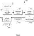
- FIG. 9illustrates a block diagram of a harvester assembly 900 according to an embodiment of the invention.
- the assembly 900includes an antenna array 901 connected to a voltage summation circuit 902.
- the voltage summation circuit 902may include an operational amplifier (op-amp).
- the antenna array 901gathers energy from microwaves each antenna of the antenna array 901 transmits the gathered energy to the voltage summation circuit 902 to combine the gathered voltage into one power signal.
- the antenna array 901may correspond to the antenna array 120 of FIGS. 1 and 4 , for example.
- the gathered energyis harvested via a resonator circuit 903 and voltage multiplier 904, such as a two-stage Dickson Charge pump.
- the resonator circuit 903, also referred to as a resonator tank,ensures that sufficient voltage swing is supplied in the power signal from the voltage summation circuit 902 to drive the rectifier stage 905.
- the resulting signalis input to a rectifier stage 905.
- the rectifier stage 905includes a three or four stage rectifier circuit. Since some power loss occurs in the rectifier circuit, due to the energy required to drive the diode junction barrier, a capacitor 906 may be provided between the rectifier 905 and a voltage regulator 907. The capacitor 906 may be selected such that the charging time of the capacitor is not more than one to three seconds, and the charge level is high. In one embodiment, multiple capacitors, or multiple super-capacitors, are connected in series.
- the rectifier 905converts the RF power from the antenna array 901 to DC power.
- the voltage regulator 907receives the rectified voltage from the rectifier stage 905 and outputs a regulated voltage at a predetermined level. The power from the voltage regulator 907 is output to a load, such as a battery.
- the harvester assembly 900includes one or more microcontrollers configured to calculate a power input level and to auto-tune a matching circuit for available RF signals at a particular frequency.
- Embodiments of the inventionencompass rectanna antennae, and in particular, arrays of spiral antennae that are parallel to each other, that spiral in opposite directions and that are connected to each other.
- a ground planeis provided between the arrays of antennae to isolate the electric fields of the antennae.
- a dielectric layeris provided between the ground plane and the arrays of antennae to increase structural strength and to increase a gain vs. frequency of the assembly.
- a rectifiersuch as a Schottky diode, connects the centers of the spiral antennae of different arrays via a hole that extends through the antenna array assembly, including ground layers, dielectric layers and balun layers.
- the Schottky diodeitself is used for the matching and filtering of the output signal.
- a transmission-line matching circuitis provided to match the optimal diode impedance for all frequencies, according to the maximum power transfer theorem.
- the dimensions of the spiral antennaemay be adjusted according to desired design characteristics.
- the diameter of the rectenna elements (or spiral antennae)satisfies the following: 0.3333 ⁇ o ⁇ L ⁇ 0.5 ⁇ o), where L is the diameter of each rectenna element and ⁇ o is the free space wavelength of a radio frequency (RF) wave.
- RFradio frequency
- the outermost periphery of the rectenna arraymust be more than 2 ⁇ g .
- the tilted beamis obtained by superimposing a radiation field between a first active region, such as a spiral antenna having a circumference of 1 ⁇ g and a second active region, such as a spiral antenna having a circumference of 2 ⁇ g .
- ⁇ ga wave length in a dielectric medium of an antenna assembly, such as the antenna assembly illustrated in FIG. 5 .
- the dielectric constant, ⁇ rof the substrate in which the antennae are housed, such as the substrate 511 of FIG. 5 , satisfies the following: 0.2 ⁇ ⁇ r ⁇ 12.
- the dielectric thickness, hsatisfies the following: 0.003 ⁇ o ⁇ h ⁇ 0.05 ⁇ .
- the number of turns of the spiral antennaedepends on an antenna impedance calculation that matches with the optimal diode impedance.
- a spiral antenna having a larger number of turns with optimal spacinghas more spectral efficiency and bandwidth.
- the circumference of the radiation zonedetermines the radiation frequency. In embodiments of the invention, the circumference of the radiation zone is greater than 2 x ⁇ o, where ⁇ o is the wavelength of the RF wave in free space.
- out of phase excitationcreates the so-called normal or the first spiral mode and the in-phase excitation creates the second mode. Since the normal mode has a single lobe broadside pattern, it requires a balanced input. This can be achieved by using a broadband balun, such as the balun layers 525 and 555 of FIG. 5 .
Landscapes
- Engineering & Computer Science (AREA)
- Computer Networks & Wireless Communication (AREA)
- Power Engineering (AREA)
- Variable-Direction Aerials And Aerial Arrays (AREA)
- Details Of Aerials (AREA)
Description
- Embodiments of the invention relate to radio frequency harvesters, and in particular to spiral antennae for harvesting RF signals to generate power.
- Numerous methods are being developed and used to harvest non-conventional or ambient energy available in nature to power small electronic devices. Examples of non-conventional power sources include solar energy, vibration energy, radio frequency (RF) energy, heat energy, etc. Some of these energy sources are ubiquitous, while others are available only at particular times or locations.
- The increasing use of wireless communication and wireless networks makes RF energy everywhere in the world. Most of the energy generated to facilitate RF communication is dissipated in the environment (e.g. air molecules, structures, organisms, etc.) Efforts are underway to capture some of this otherwise-lost RF energy to generate power.
US 3 956 752 constitutes prior art and discloses a device for harvesting and reradiating electromagnetic energy using two opposed spiral antennas.- The invention provides a device for harvesting radio frequency (RF) energy to generate power as claimed in
claim 1. - The subject matter, which is regarded as the invention, is particularly pointed out and distinctly claimed in the claims at the conclusion of the specification. The foregoing and other features, and advantages of the invention are apparent from the following detailed description taken in conjunction with the accompanying drawings in which:
FIG. 1 illustrates an antenna assembly according to an embodiment of the invention;FIG. 2 illustrates a side view of a part of an antenna assembly according to an embodiment of the invention;FIG. 3 illustrates interconnected spiral antennae according to an embodiment of the invention;FIG. 4 illustrates an antenna array according to an embodiment of the invention;FIG. 5 illustrates layers of an antenna assembly according to an embodiment of the invention;FIG. 6 illustrates layers of an antenna assembly according to another embodiment of the invention;FIG. 7 illustrates a first balun layer according to an embodiment of the invention;FIG. 8 illustrates a second balun layer according to an embodiment of the invention; andFIG. 9 illustrates a block diagram of harvester assembly according to an embodiment of the invention.- The detailed description explains embodiments of the invention, together with advantages and features, by way of example with reference to the drawings.
- Radio frequency (RF) energy is generated to communicate between RF devices, but the majority of RF energy is dissipated in the environment. Embodiments of the invention relate to harvesting RF energy with spiral antenna arrays.
FIG. 1 illustrates anantenna assembly 100 according to an embodiment of the invention. Theantenna assembly 100 includes alayer interconnect circuit 110, anantenna array 120 and aharvester circuit 130. Theantenna array 120 is a multi-layer antenna array, and thelayer interconnect circuit 110 connects the multiple layers of theantenna array 120. Theharvester circuit 130 collects the electrical energy generated by theantenna array 120 and proves an electrical outlet to provide the electrical energy to an electrical device, such as a battery or other device that runs on electricity or stores an electrical charge.FIG. 2 illustrates a side view of anantenna assembly 200 according to an embodiment of the invention. Theantenna assembly 200 includes a firstspiral antenna layer 210, a firstflat antenna layer 220, aground layer 230, a secondspiral antenna layer 250, and a secondflat antenna layer 260. The firstspiral antenna layer 210 includes threespiral antennae openings first substrate 211. The secondspiral antenna layer 250 includes threespiral antennae openings second substrate 251. The threespiral antennae spiral antennae diodes - The first flat
plate antenna layer 220 is formed on thefirst substrate 211. The first flatplate antenna layer 220 comprises a conductive material, and a separate flat plate antenna of the flatplate antenna layer 220 may be positioned above eachspiral antenna plate antenna layer 260 is formed on thesecond substrate 251. The flatplate antenna layers FIG. 4 . - The
ground layer 230 includes asubstrate 231 andground plate 232. Theground plate 232 may be a conductive plate having holes cut into the plate to pass conductive lines connecting the firstspiral antennae conductive antennae spiral antenna layers ground plate 232, the radiation fields of the spiral antennae of therespective layers FIG. 3 illustrates connectedspiral antennae spiral antennae FIG. 3 , the firstspiral antenna 212a spirals in a counter-clockwise direction (CCW) and the secondspiral antenna 252a spirals in a clockwise direction (CW) from its center outward. In embodiments of the invention, thespiral antennae diode 240a form a rectanna, which is an antenna that detects or receives microwaves and generates a direct current (DC) output based on the detected or received microwaves. The Schottkydiode 240a rectifies the signals generated by thespiral antennae diode 240a.- In embodiments of the invention, the spirals of the
spiral antennae - In addition, as illustrated in
FIGS. 2 and3 , the connected spiral antennae, such asspiral antennae antennae FIG. 2 , theground plate 232 or 272 between the connected spiral antennae electromagnetic interaction due to parallelism of spirals having opposite polarities. Further, whileFIG. 2 illustrates different antennae, plates and layers of varying thicknesses, the illustrated thicknesses and sizes are for purposes of illustration only, and embodiments of the invention are not limited to sizes or proportions illustrated inFIG. 2 . FIG. 4 illustrates anantenna array 120 according to an embodiment of the invention. Theantenna array 120 includesantenna modules antenna module 410 will be described in further detail, although the characteristics of theantenna module 410 are the same as the characteristics of theantenna modules antenna modules spiral antennae FIG. 2 .- The
antenna module 410 includes aspiral antenna 411 andflat plate antennae flat plate antennae plate antenna layer 220 ofFIG. 2 . Theflat plate antenna 415 includes an output connected to an adjacent flat plate antenna of theantenna module 420, and theflat plate antenna 414 includes an output connected to a different flat plate antenna of the antenna module 460.Thespiral antenna 411 includes afirst end connector 412 connected to alayer interconnect circuit 110 and acenter connector 413 connected to a spiral antenna located on an opposite side of a spiral antenna assembly from thespiral antenna 411, as illustrated inFIG. 2 . - The
flat plate antennae patch antennae spiral antenna 411. Theflat plate antennae spiral antenna 411 along a circumference of thespiral antenna 411, or in a radial direction with respect to the center of thespiral antenna 411.FIG. 2 illustrates the flatplate antenna layer 220 located on top of thesubstrate 211 for purposes of description. However, embodiments encompass flat plate antennae that are inserted into grooves in asubstrate 211 to have an outer surface that is substantially flush with the outer surface of thesubstrate 211. Theflat plate antennae spiral antenna 411 broadband characteristics by improving a frequency vs. impedance curve of thespiral antenna 411. - The outputs from the
antenna modules 410 to 490, including thespiral antennae 411 and thepatch antennae antenna module 410 to 490, are output to thelayer interconnect circuit 110, which is a printed circuit in electrical communication with thearray 120. In one embodiment, thelayer interconnect circuit 110 is printed on the same substrate in which theantennae modules 410 to 490 are located. Thesubstrate 401 may be, for example, a printed wiring board. FIG. 5 illustrates a cross-section view of layers of anantenna assembly 500 according to an embodiment of the invention. The antenna assembly includes a firstspiral antenna layer 510 including asubstrate 511,spiral antennae patch antennae 516. Thesubstrate 511 may be made of any electrically insulating material, such as a printed circuit board (PCB), resin, semiconductor material, or any other electrically insulating material. Theantennae patch antennae 516 may be made of any conductive material, such as copper, aluminum, gold, silver, or any other conductive material or alloy. Theantenna patch antennae 516 may be pre-formed and deposited on thesubstrate 511, may be formed by photolithography or chemical deposition on thesubstrate 511, or may be formed or deposited by any other process.- Below the first
spiral antenna layer 510 is a firstthin dielectric layer 520. Below the firstthin dielectric layer 520 is afirst balun layer 525. Thefirst balun layer 525 includesbalun wiring 527 on asubstrate 526. Below thefirst balun layer 525 is a secondthin dielectric layer 530. Below thethin dielectric layer 530 is aground layer 535, including a conductive ground plate or wiring. - The
antenna assembly 500 further includes a secondspiral antenna layer 540 including asubstrate 541,spiral antennae patch antennae 546. Above the secondspiral antenna layer 540 is a thirdthin dielectric layer 550. Above the thirdthin dielectric layer 550 is asecond balun layer 555. Thesecond balun layer 555 includesbalun wiring 557 on asubstrate 556. Above thesecond balun layer 555 is a fourththin dielectric layer 530. Above the fourththin dielectric layer 560 is theground layer 535. - As illustrated in
FIG. 5 , all of thelayers channels spiral antennae 512a to 512c and thespiral antennae 542a to 542c. Arectifier spiral antennae 512a to 512c and thespiral antennae 542a to 542c. In one embodiment, therectifiers 515a to 515c are Schottky diodes. Although therectifiers 515a to 515c are illustrated as being within thechannels 513a to 513c, embodiments of the invention encompass any configuration in which therectifiers 515a to 515c are located electrically between thespiral antennae 512a to 512c and thespiral antennae 542a to 542c. For example, therectifiers 515a to 515c may be circuit elements mounted onto, or within, one of thedielectric layers substrates FIG. 5 illustrates a wire orline 514 extending through thechannel 513a, embodiments of the invention encompass any method of electrical connection, such as providing a conductive filling material to fill thechannels 513a to 513c. - While the connections between the
spiral antennae 512a to 512c and thespiral antennae 542a to 542c are illustrated inFIG. 5 , it is understood that theantenna assembly 500 includes additional electrical and physical connections between various layers, including between thespiral antennae 512a to 512c and thefirst balun circuit 527, or balun wiring layer, and between thefirst balun circuit 527 and the first ground plate 537. - While the terms "above" and "below" have been used to describe the layers in view of
FIG. 5 , it is understood that embodiments of the invention encompass devices having layers arranged as inFIG. 5 , but having any orientations, such as at an angle greater than zero with respect toFIG. 5 . In addition, embodiments of the invention encompass antenna assemblies having additional layers or layers omitted, relative toFIG. 5 . In one embodiment, the total thickness of the antenna assembly, such as theassembly 500 ofFIG. 5 , satisfies the following: 0.006λo < h <= 0.05λο, where λo is the wavelength of a radio frequency (RF) wave in free space. FIG. 6 illustrates a cross-section view of layers of anantenna assembly 600 according to an embodiment of the invention. The antenna assembly includes a firstspiral antenna layer 610 including asubstrate 611 andspiral antennae modules substrate 611 may be made of any electrically insulating material, such as a printed circuit board (PCB), resin, semiconductor material, or any other electrically insulating material. Theantennae modules layer substrate 611, forms acavity spiral antenna layer Patch antennae 614a, 614b or 614c are formed to surround thespiral antenna layer patch antennae 614a, 614b and 614c are also configured to surround lateral sides of the dielectric insulatinglayers patch antennae 614a, 614b or 614c is located on the same surface of the dielectric insulatinglayers spiral antennae patch antennae 614a, 614b or 614c is located on lateral sides of the dielectric insulatinglayers - Below the first
spiral antenna layer 610 is a firstthin dielectric layer 620. Below the firstthin dielectric layer 620 is afirst balun layer 630. Below thefirst balun layer 620 is a secondthin dielectric layer 630. Below the secondthin dielectric layer 630 is aground layer 640, which may be a conductive plate. Theantenna assembly 600 further includes a secondspiral antenna layer 670 including asubstrate 671 andspiral antennae modules substrate 671 may be made of any electrically insulating material, such as a printed circuit board (PCB), resin, semiconductor material, or any other electrically insulating material. Theantennae modules layer spiral antenna layer Patch antennae spiral antenna layer patch antennae layers - As illustrated in
FIG. 6 , all of thelayers channels 681. For purposes of clarity, only thechannel 681 extending between thespiral antennae FIG. 6 , but each opposing pair ofantennae conductive line 682 extending throughchannels 681 in thelayers insulator 683 surrounds theconductive line 682 within thechannel 681 at locations corresponding to theground layer 640 andbalun layers conductive line 682 and thelayers - In one embodiment, a
rectifier spiral antennae spiral antennae rectifier spiral antennae 613a to 613c and thespiral antennae 673a to 673c. - In one embodiment, the
spiral antenna modules 612a to 612c and 672a to 672c are readily connectable and disconnectable from theconductive line 682. As illustrated inFIG. 6 , theconductive line 682 has aconnector 684 that is located to connect to aconnector 685 of eachspiral antenna module 612a to 612c and 672a to 672c. Theconnectors spiral antenna modules 612a to 612c and 672a to 672c may be connected to the substrates 711 and 771 or theconductive line 682 by adhesives, soldering or any other permanent connection process. - While the various layers and other features have been illustrated in
FIG. 6 with different thicknesses, it is understood that the thicknesses and lengths of materials and features ofFIG. 6 are provided by way of illustration only, and embodiments of the invention are not limited to the specific widths, lengths, thicknesses or relative dimensions illustrated inFIG. 6 . FIG. 7 illustrates afirst balun layer 525 according to an embodiment of the invention. The balun layer illustrated inFIG. 7 may also correspond to thefirst balun layer 620 illustrated inFIG. 6 . Thefirst balun layer 525 includes thesubstrate 526 and thebalun wiring 527. Thebalun wiring 527 may be any conductive material, such as copper, aluminum, etc. Thebalun wiring 527 may be printed on thesubstrate 526 via photolithography, etching, deposition, or any other method. Thebalun wiring 527 includes aninput 528 from the firstspiral antenna layer 510, and in particular from thespiral antennae balun wiring 527 also includesoutputs 529 to a harvester circuit (not shown inFIG. 7 ). Thebalun wiring 556 is also connected to ground, such as the ground plate 537. Thebalun wiring 527 is configured to match the impedance of thespiral antennae 512a to 512c with the harvester circuit.FIG. 8 illustrates asecond balun layer 555 according to embodiments of the invention. The balun layer illustrated inFIG. 8 may also correspond to thesecond balun layer 660 ofFIG. 6 . Thesecond balun layer 555 includes asubstrate 557 andbalun wiring 556. Thebalun wiring 556 includes aninput 558 from the secondspiral antenna layer 540, and in particular from thespiral antennae balun wiring 556 also includesoutputs 559 to a harvester circuit (not shown inFIG. 8 ). Thebalun wiring 556 is also connected to ground, such as the ground plate 566. Thebalun wiring 556 is configured to match the impedance of thespiral antennae 542a to 542c with the harvester circuit.- In embodiments of the invention, the
balun wirings balun wirings balun wirings balun wirings baluns spiral antennae 512a to 512c and 542a to 542c) to a balanced transmission line at the output. Thebalun wirings - The
balun wirings balun wirings - As illustrated in
FIGS. 7 and8 , theinput lines balun wirings balun wirings - Referring to
FIGS. 4 ,5 ,7 and8 thelayer interconnect circuit 110 ofFIG. 4 connects the outputs from thespiral antennae modules 410 to 490, including thespiral antennae 411 and thepatch antennae outputs 412 of all of thespiral antennae 411 of eachplanar array 120, are interconnected. For example, thearray 120 illustrated inFIG. 4 is one array corresponding to the firstspiral antenna layer 510 ofFIG. 5 and the secondspiral antenna layer 540 includes a similar array having spiral antenna with spirals of an opposite direction. In such an embodiment, all of the spiral antennae of the firstspiral antenna layer 510 are connected to each other, and all of the spiral antennae of the secondspiral antenna layer 540 are connected to each other. The outputs from the spiral antennae of the firstspiral antenna layer 510 comprise oneinput 528 of thefirst balun wiring 525 and oneinput 558 of thesecond balun wiring 555. Similarly, the outputs from the spiral antennae of the secondspiral antenna layer 540 comprise oneinput 528 of thefirst balun wiring 525 and oneinput 558 of thesecond balun wiring 555. - In one embodiment, the wiring of the
interconnect circuit 110 connects the spiral antennae of the firstspiral antenna layer 510 and the spiral antennae of the secondspiral antenna layer 540 together in series, such that all of the spiral antennae of theantenna assembly 500 are connected in series, and ends of the spiral antennae are connected to thebalun wirings patch antennae FIG. 9 illustrates a block diagram of aharvester assembly 900 according to an embodiment of the invention. Theassembly 900 includes anantenna array 901 connected to avoltage summation circuit 902. Thevoltage summation circuit 902 may include an operational amplifier (op-amp). Theantenna array 901 gathers energy from microwaves each antenna of theantenna array 901 transmits the gathered energy to thevoltage summation circuit 902 to combine the gathered voltage into one power signal. Theantenna array 901 may correspond to theantenna array 120 ofFIGS. 1 and4 , for example. The gathered energy is harvested via aresonator circuit 903 andvoltage multiplier 904, such as a two-stage Dickson Charge pump. Theresonator circuit 903, also referred to as a resonator tank, ensures that sufficient voltage swing is supplied in the power signal from thevoltage summation circuit 902 to drive therectifier stage 905.- The resulting signal is input to a
rectifier stage 905. In one embodiment, therectifier stage 905 includes a three or four stage rectifier circuit. Since some power loss occurs in the rectifier circuit, due to the energy required to drive the diode junction barrier, acapacitor 906 may be provided between therectifier 905 and avoltage regulator 907. Thecapacitor 906 may be selected such that the charging time of the capacitor is not more than one to three seconds, and the charge level is high. In one embodiment, multiple capacitors, or multiple super-capacitors, are connected in series. Therectifier 905 converts the RF power from theantenna array 901 to DC power. Thevoltage regulator 907 receives the rectified voltage from therectifier stage 905 and outputs a regulated voltage at a predetermined level. The power from thevoltage regulator 907 is output to a load, such as a battery. - In one embodiment, the
harvester assembly 900 includes one or more microcontrollers configured to calculate a power input level and to auto-tune a matching circuit for available RF signals at a particular frequency. - Embodiments of the invention encompass rectanna antennae, and in particular, arrays of spiral antennae that are parallel to each other, that spiral in opposite directions and that are connected to each other. A ground plane is provided between the arrays of antennae to isolate the electric fields of the antennae. A dielectric layer is provided between the ground plane and the arrays of antennae to increase structural strength and to increase a gain vs. frequency of the assembly.
- A rectifier, such as a Schottky diode, connects the centers of the spiral antennae of different arrays via a hole that extends through the antenna array assembly, including ground layers, dielectric layers and balun layers. In some embodiments, the Schottky diode itself is used for the matching and filtering of the output signal. However, in some embodiments of the invention, a transmission-line matching circuit is provided to match the optimal diode impedance for all frequencies, according to the maximum power transfer theorem.
- The dimensions of the spiral antennae may be adjusted according to desired design characteristics. In one embodiment, the diameter of the rectenna elements (or spiral antennae) satisfies the following: 0.3333 λo < L < 0.5 λo), where L is the diameter of each rectenna element and λo is the free space wavelength of a radio frequency (RF) wave. To obtain a tilt beams, the outermost periphery of the rectenna array must be more than 2λg. The tilted beam is obtained by superimposing a radiation field between a first active region, such as a spiral antenna having a circumference of 1λg and a second active region, such as a spiral antenna having a circumference of 2λg. Here, λg = a wave length in a dielectric medium of an antenna assembly, such as the antenna assembly illustrated in
FIG. 5 . In embodiments of the invention, the dielectric constant, εr, of the substrate in which the antennae are housed, such as thesubstrate 511 ofFIG. 5 , satisfies the following: 0.2 < εr < 12. In addition, the dielectric thickness,h, satisfies the following: 0.003λo<h<0.05λο. - The number of turns of the spiral antennae depends on an antenna impedance calculation that matches with the optimal diode impedance. A spiral antenna having a larger number of turns with optimal spacing has more spectral efficiency and bandwidth. The circumference of the radiation zone determines the radiation frequency. In embodiments of the invention, the circumference of the radiation zone is greater than 2 x λo, where λo is the wavelength of the RF wave in free space.
- There are two possible excitations for spiral antennae: out of phase excitation (balanced) and in-phase excitation. The out of phase excitation creates the so-called normal or the first spiral mode and the in-phase excitation creates the second mode. Since the normal mode has a single lobe broadside pattern, it requires a balanced input. This can be achieved by using a broadband balun, such as the balun layers 525 and 555 of
FIG. 5 . - While the invention has been described in detail in connection with only a limited number of embodiments, it should be readily understood that the invention is not limited to such disclosed embodiments. Additionally, while various embodiments of the invention have been described, it is to be understood that aspects of the invention may include only some of the described embodiments. Accordingly, the invention is not to be seen as limited by the foregoing description, but is only limited by the scope of the appended claims.
Claims (8)
- A device for harvesting radio frequency RF, energy to generate power, comprising:a first spiral antenna (212a; 212b; 212c) having a first spiral direction, the first spiral antenna (212a; 212b; 212c) having a spiral cross-section shape along a first flat plane;a second spiral antenna (252a; 252b; 252c) having a second spiral direction opposite the first spiral direction, the second spiral (252a; 252b; 252c) antenna having a spiral cross-section shape along a second plane parallel to the first plane;a ground layer (230) between the first and second spiral antennae (212; 252), the first spiral antenna (212a; 212b; 212c) electrically connected to the second spiral antenna (252a; 252b; 252c) at a center of the first and second spiral antennae by a conductive element passing through the ground layer (230) without contacting a conductive ground plate of the ground layer (230);characterised by:a first dielectric layer surrounding the first spiral antenna (212a; 212b; 212c) along the first flat plane; anda first flat antenna (220) mounted to the first dielectric layer, the first flat antenna (220) defining a fourth plane parallel to the first flat plane.
- The device of claim 1, wherein the conductive element includes a Schottky diode.
- The device of claim 1, wherein the ground layer defines a third plane parallel to the first flat plane and the second plane.
- The device of claim 1, wherein the first dielectric layer has a thickness greater than a thickness of the first spiral antenna, such that the fourth plane does not intersect the first flat plane.
- The device of claim 1, further comprising:a first balun layer between the first spiral antenna and the ground layer, the first balun layer electrically connected to the first spiral antenna and the ground layer; anda second balun layer between the second spiral antenna and the ground layer, the second balun layer electrically connected to the second spiral antenna.
- The device of claim 5, further comprising:
a harvester circuit connected to the outputs of the first and second balun layers, the harvester circuit configured to receive a radio frequency signal gathered by the first and second spiral antennae and to generate a direct current signal based on the radio frequency signal. - The device of claim 1, wherein the first spiral antenna includes a first array of multiple first spiral antennae arranged along the same first flat plane, and
the second spiral antenna includes a second array of multiple second spiral antennae arranged along the same second plane. - The device of claim 7, wherein the multiple first spiral antennae and the multiple second spiral antennae are arranged in series electrically.
Applications Claiming Priority (2)
| Application Number | Priority Date | Filing Date | Title |
|---|---|---|---|
| US201361843667P | 2013-07-08 | 2013-07-08 | |
| PCT/US2014/045572WO2015006214A1 (en) | 2013-07-08 | 2014-07-07 | Radio frequency harvester assembly |
Publications (2)
| Publication Number | Publication Date |
|---|---|
| EP3020092A1 EP3020092A1 (en) | 2016-05-18 |
| EP3020092B1true EP3020092B1 (en) | 2020-04-29 |
Family
ID=51213068
Family Applications (1)
| Application Number | Title | Priority Date | Filing Date |
|---|---|---|---|
| EP14742131.7AActiveEP3020092B1 (en) | 2013-07-08 | 2014-07-07 | Radio frequency harvester assembly |
Country Status (4)
| Country | Link |
|---|---|
| US (1) | US10014730B2 (en) |
| EP (1) | EP3020092B1 (en) |
| ES (1) | ES2788626T3 (en) |
| WO (1) | WO2015006214A1 (en) |
Families Citing this family (19)
| Publication number | Priority date | Publication date | Assignee | Title |
|---|---|---|---|---|
| US20160308402A1 (en)* | 2015-04-20 | 2016-10-20 | Babak Alavikia | Electromagnetic Energy Harvesting Using Complementary Split-Ring Resonators |
| US10355368B2 (en)* | 2016-05-26 | 2019-07-16 | King Abdulaziz City For Science And Technology | Energy harvesting device composed of electrically small particles |
| IL246003B (en) | 2016-06-02 | 2019-03-31 | W P Energy Ltd | Multiband energy harvesting |
| US11071857B2 (en) | 2016-08-22 | 2021-07-27 | William Marsh Rice University | Systems and methods for wireless treatment of arrhythmias |
| CN206602182U (en)* | 2017-04-06 | 2017-10-31 | 京东方科技集团股份有限公司 | A kind of antenna structure and communication apparatus |
| US11133580B2 (en)* | 2017-06-22 | 2021-09-28 | Innolux Corporation | Antenna device |
| EP3676937A4 (en) | 2017-09-01 | 2021-06-02 | Powercast Corporation | Methods, systems, and apparatus for automatic rf power transmission and single antenna energy harvesting |
| CN110365422B (en)* | 2018-04-04 | 2021-01-29 | 京东方科技集团股份有限公司 | Signal processing device and preparation method thereof |
| US10784590B2 (en)* | 2018-07-06 | 2020-09-22 | Bae Systems Information And Electronic Systems Integration Inc. | Ultra-wide bandwidth frequency-independent circularly polarized array antenna |
| US12320769B2 (en) | 2018-11-19 | 2025-06-03 | The Regents Of The University Of California | Systems and methods for battery-less wirelessly powered dielectric sensors |
| CN113228464A (en) | 2018-11-20 | 2021-08-06 | 加利福尼亚大学董事会 | System and method for controlling a wirelessly powered leadless pacemaker |
| TWI703789B (en)* | 2018-12-25 | 2020-09-01 | 力能科技有限公司 | Power supply device and method of use thereof |
| WO2020141291A1 (en)* | 2019-01-04 | 2020-07-09 | The Secretary Of State For Defence | Electromagnetic pulse detector and method of use |
| JP7159943B2 (en)* | 2019-03-28 | 2022-10-25 | 富士通株式会社 | power converter |
| EP3991247B1 (en) | 2019-06-26 | 2025-09-17 | The Regents of the University of California | Thz impulse and frequency comb generation using reverse recovery of pin diode |
| US12052533B2 (en) | 2019-07-08 | 2024-07-30 | The Regents Of The University Of California | Systems and methods for long-distance remote sensing with sub-wavelength resolution using a wirelessly-powered sensor tag array |
| KR102790323B1 (en) | 2019-08-23 | 2025-04-07 | 주식회사 시솔지주 | Fingerprint congnition card |
| JP2023515580A (en) | 2020-02-28 | 2023-04-13 | ザ リージェンツ オブ ザ ユニバーシティ オブ カリフォルニア | Integrated Energy Recovery Transceiver and Transmitter with Dual Antenna Architecture for Microimplants and Electrochemical Sensors |
| CN120527610B (en)* | 2025-07-25 | 2025-10-03 | 湖南先进技术研究院 | Circularly polarized antenna array |
Family Cites Families (18)
| Publication number | Priority date | Publication date | Assignee | Title |
|---|---|---|---|---|
| US3956752A (en) | 1975-03-12 | 1976-05-11 | Harris Corporation | Polarization insensitive lens formed of spiral radiators |
| US4087821A (en)* | 1976-07-14 | 1978-05-02 | Harris Corporation | Polarization controllable lens |
| US4943811A (en) | 1987-11-23 | 1990-07-24 | Canadian Patents And Development Limited | Dual polarization electromagnetic power reception and conversion system |
| CA1307842C (en) | 1988-12-28 | 1992-09-22 | Adrian William Alden | Dual polarization microstrip array antenna |
| CA2006481C (en) | 1989-12-19 | 1999-09-21 | Adrian W. Alden | Low noise dual polarization electromagnetic power reception and conversion system |
| CA2011298C (en) | 1990-03-01 | 1999-05-25 | Adrian William Alden | Dual polarization dipole array antenna |
| WO1997002623A1 (en) | 1995-07-05 | 1997-01-23 | California Institute Of Technology | A dual polarized, heat spreading rectenna |
| US6369759B1 (en) | 1999-06-09 | 2002-04-09 | California Institute Of Technology | Rectenna for high-voltage applications |
| US6882128B1 (en) | 2000-09-27 | 2005-04-19 | Science Applications International Corporation | Method and system for energy reclamation and reuse |
| US8228194B2 (en) | 2004-10-28 | 2012-07-24 | University Of Pittsburgh - Of The Commonwealth System Of Higher Education | Recharging apparatus |
| US20070298846A1 (en) | 2006-06-14 | 2007-12-27 | Powercast, Llc | Wireless power transmission |
| KR100912063B1 (en) | 2007-07-26 | 2009-08-12 | 한국전기연구원 | High Efficiency Wireless Power Supply Using Dual Frequency Bands |
| US20090117872A1 (en) | 2007-11-05 | 2009-05-07 | Jorgenson Joel A | Passively powered element with multiple energy harvesting and communication channels |
| US8115683B1 (en) | 2008-05-06 | 2012-02-14 | University Of South Florida | Rectenna solar energy harvester |
| CA2785181C (en) | 2010-01-07 | 2018-01-02 | Voxx International Corporation | Method and apparatus for harvesting energy |
| US8330298B2 (en) | 2010-06-17 | 2012-12-11 | Scarf Technologies Llc | Generating DC electric power from ambient electromagnetic radiation |
| IT1402247B1 (en) | 2010-09-27 | 2013-08-28 | Eurotech S P A | ELECTROMAGNETIC ENERGY CONVERSION DEVICE FOR RADIOFREQUENCY |
| US10074888B2 (en)* | 2015-04-03 | 2018-09-11 | NXT-ID, Inc. | Accordion antenna structure |
- 2014
- 2014-07-07EPEP14742131.7Apatent/EP3020092B1/enactiveActive
- 2014-07-07WOPCT/US2014/045572patent/WO2015006214A1/enactiveApplication Filing
- 2014-07-07USUS14/903,322patent/US10014730B2/enactiveActive
- 2014-07-07ESES14742131Tpatent/ES2788626T3/enactiveActive
Non-Patent Citations (1)
| Title |
|---|
| None* |
Also Published As
| Publication number | Publication date |
|---|---|
| US20160149441A1 (en) | 2016-05-26 |
| WO2015006214A1 (en) | 2015-01-15 |
| US10014730B2 (en) | 2018-07-03 |
| EP3020092A1 (en) | 2016-05-18 |
| ES2788626T3 (en) | 2020-10-22 |
Similar Documents
| Publication | Publication Date | Title |
|---|---|---|
| EP3020092B1 (en) | Radio frequency harvester assembly | |
| US11862879B2 (en) | Antenna elements and array | |
| US20210376484A1 (en) | Substrate-loaded frequency-scaled ultra-wide spectrum element | |
| US8842054B2 (en) | Grid array antennas and an integration structure | |
| US9991605B2 (en) | Frequency-scaled ultra-wide spectrum element | |
| US10431903B2 (en) | Antenna systems with low passive intermodulation (PIM) | |
| US6806839B2 (en) | Wide bandwidth flat panel antenna array | |
| US20160094091A1 (en) | Wideband rectenna and rectifying apparatus for rectenna | |
| CN108292807A (en) | Luneburg lens antenna device | |
| CN101065883A (en) | Quadrifilar helical antenna | |
| JP6001071B2 (en) | Loop antenna | |
| US9705194B2 (en) | Antenna module | |
| US10090595B2 (en) | Broadband rectenna | |
| WO2019111025A1 (en) | Antenna | |
| JP5562080B2 (en) | antenna | |
| JP2006186436A (en) | Dielectric resonator antenna, wiring board, and electronic device | |
| WO2009133523A1 (en) | Multifunctional antenna module for use with a multiplicity of radiofrequency signals | |
| WO2019181169A1 (en) | Antenna device | |
| IL249791A (en) | Antenna element |
Legal Events
| Date | Code | Title | Description |
|---|---|---|---|
| PUAI | Public reference made under article 153(3) epc to a published international application that has entered the european phase | Free format text:ORIGINAL CODE: 0009012 | |
| 17P | Request for examination filed | Effective date:20160203 | |
| AK | Designated contracting states | Kind code of ref document:A1 Designated state(s):AL AT BE BG CH CY CZ DE DK EE ES FI FR GB GR HR HU IE IS IT LI LT LU LV MC MK MT NL NO PL PT RO RS SE SI SK SM TR | |
| AX | Request for extension of the european patent | Extension state:BA ME | |
| DAX | Request for extension of the european patent (deleted) | ||
| STAA | Information on the status of an ep patent application or granted ep patent | Free format text:STATUS: EXAMINATION IS IN PROGRESS | |
| 17Q | First examination report despatched | Effective date:20190524 | |
| GRAP | Despatch of communication of intention to grant a patent | Free format text:ORIGINAL CODE: EPIDOSNIGR1 | |
| STAA | Information on the status of an ep patent application or granted ep patent | Free format text:STATUS: GRANT OF PATENT IS INTENDED | |
| INTG | Intention to grant announced | Effective date:20191213 | |
| GRAS | Grant fee paid | Free format text:ORIGINAL CODE: EPIDOSNIGR3 | |
| GRAA | (expected) grant | Free format text:ORIGINAL CODE: 0009210 | |
| STAA | Information on the status of an ep patent application or granted ep patent | Free format text:STATUS: THE PATENT HAS BEEN GRANTED | |
| AK | Designated contracting states | Kind code of ref document:B1 Designated state(s):AL AT BE BG CH CY CZ DE DK EE ES FI FR GB GR HR HU IE IS IT LI LT LU LV MC MK MT NL NO PL PT RO RS SE SI SK SM TR | |
| REG | Reference to a national code | Ref country code:GB Ref legal event code:FG4D | |
| REG | Reference to a national code | Ref country code:CH Ref legal event code:EP | |
| REG | Reference to a national code | Ref country code:AT Ref legal event code:REF Ref document number:1264687 Country of ref document:AT Kind code of ref document:T Effective date:20200515 | |
| REG | Reference to a national code | Ref country code:DE Ref legal event code:R096 Ref document number:602014064511 Country of ref document:DE Ref country code:NL Ref legal event code:FP | |
| REG | Reference to a national code | Ref country code:IE Ref legal event code:FG4D | |
| REG | Reference to a national code | Ref country code:LT Ref legal event code:MG4D | |
| REG | Reference to a national code | Ref country code:ES Ref legal event code:FG2A Ref document number:2788626 Country of ref document:ES Kind code of ref document:T3 Effective date:20201022 | |
| PG25 | Lapsed in a contracting state [announced via postgrant information from national office to epo] | Ref country code:SE Free format text:LAPSE BECAUSE OF FAILURE TO SUBMIT A TRANSLATION OF THE DESCRIPTION OR TO PAY THE FEE WITHIN THE PRESCRIBED TIME-LIMIT Effective date:20200429 Ref country code:NO Free format text:LAPSE BECAUSE OF FAILURE TO SUBMIT A TRANSLATION OF THE DESCRIPTION OR TO PAY THE FEE WITHIN THE PRESCRIBED TIME-LIMIT Effective date:20200729 Ref country code:FI Free format text:LAPSE BECAUSE OF FAILURE TO SUBMIT A TRANSLATION OF THE DESCRIPTION OR TO PAY THE FEE WITHIN THE PRESCRIBED TIME-LIMIT Effective date:20200429 Ref country code:GR Free format text:LAPSE BECAUSE OF FAILURE TO SUBMIT A TRANSLATION OF THE DESCRIPTION OR TO PAY THE FEE WITHIN THE PRESCRIBED TIME-LIMIT Effective date:20200730 Ref country code:IS Free format text:LAPSE BECAUSE OF FAILURE TO SUBMIT A TRANSLATION OF THE DESCRIPTION OR TO PAY THE FEE WITHIN THE PRESCRIBED TIME-LIMIT Effective date:20200829 Ref country code:PT Free format text:LAPSE BECAUSE OF FAILURE TO SUBMIT A TRANSLATION OF THE DESCRIPTION OR TO PAY THE FEE WITHIN THE PRESCRIBED TIME-LIMIT Effective date:20200831 Ref country code:LT Free format text:LAPSE BECAUSE OF FAILURE TO SUBMIT A TRANSLATION OF THE DESCRIPTION OR TO PAY THE FEE WITHIN THE PRESCRIBED TIME-LIMIT Effective date:20200429 | |
| REG | Reference to a national code | Ref country code:AT Ref legal event code:MK05 Ref document number:1264687 Country of ref document:AT Kind code of ref document:T Effective date:20200429 | |
| PG25 | Lapsed in a contracting state [announced via postgrant information from national office to epo] | Ref country code:HR Free format text:LAPSE BECAUSE OF FAILURE TO SUBMIT A TRANSLATION OF THE DESCRIPTION OR TO PAY THE FEE WITHIN THE PRESCRIBED TIME-LIMIT Effective date:20200429 Ref country code:LV Free format text:LAPSE BECAUSE OF FAILURE TO SUBMIT A TRANSLATION OF THE DESCRIPTION OR TO PAY THE FEE WITHIN THE PRESCRIBED TIME-LIMIT Effective date:20200429 Ref country code:BG Free format text:LAPSE BECAUSE OF FAILURE TO SUBMIT A TRANSLATION OF THE DESCRIPTION OR TO PAY THE FEE WITHIN THE PRESCRIBED TIME-LIMIT Effective date:20200729 Ref country code:RS Free format text:LAPSE BECAUSE OF FAILURE TO SUBMIT A TRANSLATION OF THE DESCRIPTION OR TO PAY THE FEE WITHIN THE PRESCRIBED TIME-LIMIT Effective date:20200429 | |
| PG25 | Lapsed in a contracting state [announced via postgrant information from national office to epo] | Ref country code:AL Free format text:LAPSE BECAUSE OF FAILURE TO SUBMIT A TRANSLATION OF THE DESCRIPTION OR TO PAY THE FEE WITHIN THE PRESCRIBED TIME-LIMIT Effective date:20200429 | |
| PG25 | Lapsed in a contracting state [announced via postgrant information from national office to epo] | Ref country code:CZ Free format text:LAPSE BECAUSE OF FAILURE TO SUBMIT A TRANSLATION OF THE DESCRIPTION OR TO PAY THE FEE WITHIN THE PRESCRIBED TIME-LIMIT Effective date:20200429 Ref country code:RO Free format text:LAPSE BECAUSE OF FAILURE TO SUBMIT A TRANSLATION OF THE DESCRIPTION OR TO PAY THE FEE WITHIN THE PRESCRIBED TIME-LIMIT Effective date:20200429 Ref country code:SM Free format text:LAPSE BECAUSE OF FAILURE TO SUBMIT A TRANSLATION OF THE DESCRIPTION OR TO PAY THE FEE WITHIN THE PRESCRIBED TIME-LIMIT Effective date:20200429 Ref country code:IT Free format text:LAPSE BECAUSE OF FAILURE TO SUBMIT A TRANSLATION OF THE DESCRIPTION OR TO PAY THE FEE WITHIN THE PRESCRIBED TIME-LIMIT Effective date:20200429 Ref country code:EE Free format text:LAPSE BECAUSE OF FAILURE TO SUBMIT A TRANSLATION OF THE DESCRIPTION OR TO PAY THE FEE WITHIN THE PRESCRIBED TIME-LIMIT Effective date:20200429 Ref country code:DK Free format text:LAPSE BECAUSE OF FAILURE TO SUBMIT A TRANSLATION OF THE DESCRIPTION OR TO PAY THE FEE WITHIN THE PRESCRIBED TIME-LIMIT Effective date:20200429 Ref country code:AT Free format text:LAPSE BECAUSE OF FAILURE TO SUBMIT A TRANSLATION OF THE DESCRIPTION OR TO PAY THE FEE WITHIN THE PRESCRIBED TIME-LIMIT Effective date:20200429 | |
| REG | Reference to a national code | Ref country code:DE Ref legal event code:R097 Ref document number:602014064511 Country of ref document:DE | |
| PG25 | Lapsed in a contracting state [announced via postgrant information from national office to epo] | Ref country code:SK Free format text:LAPSE BECAUSE OF FAILURE TO SUBMIT A TRANSLATION OF THE DESCRIPTION OR TO PAY THE FEE WITHIN THE PRESCRIBED TIME-LIMIT Effective date:20200429 Ref country code:MC Free format text:LAPSE BECAUSE OF FAILURE TO SUBMIT A TRANSLATION OF THE DESCRIPTION OR TO PAY THE FEE WITHIN THE PRESCRIBED TIME-LIMIT Effective date:20200429 Ref country code:PL Free format text:LAPSE BECAUSE OF FAILURE TO SUBMIT A TRANSLATION OF THE DESCRIPTION OR TO PAY THE FEE WITHIN THE PRESCRIBED TIME-LIMIT Effective date:20200429 | |
| REG | Reference to a national code | Ref country code:CH Ref legal event code:PL | |
| PLBE | No opposition filed within time limit | Free format text:ORIGINAL CODE: 0009261 | |
| STAA | Information on the status of an ep patent application or granted ep patent | Free format text:STATUS: NO OPPOSITION FILED WITHIN TIME LIMIT | |
| 26N | No opposition filed | Effective date:20210201 | |
| REG | Reference to a national code | Ref country code:BE Ref legal event code:MM Effective date:20200731 | |
| PG25 | Lapsed in a contracting state [announced via postgrant information from national office to epo] | Ref country code:LU Free format text:LAPSE BECAUSE OF NON-PAYMENT OF DUE FEES Effective date:20200707 Ref country code:LI Free format text:LAPSE BECAUSE OF NON-PAYMENT OF DUE FEES Effective date:20200731 Ref country code:IE Free format text:LAPSE BECAUSE OF NON-PAYMENT OF DUE FEES Effective date:20200707 Ref country code:CH Free format text:LAPSE BECAUSE OF NON-PAYMENT OF DUE FEES Effective date:20200731 | |
| PG25 | Lapsed in a contracting state [announced via postgrant information from national office to epo] | Ref country code:BE Free format text:LAPSE BECAUSE OF NON-PAYMENT OF DUE FEES Effective date:20200731 Ref country code:SI Free format text:LAPSE BECAUSE OF FAILURE TO SUBMIT A TRANSLATION OF THE DESCRIPTION OR TO PAY THE FEE WITHIN THE PRESCRIBED TIME-LIMIT Effective date:20200429 | |
| PG25 | Lapsed in a contracting state [announced via postgrant information from national office to epo] | Ref country code:TR Free format text:LAPSE BECAUSE OF FAILURE TO SUBMIT A TRANSLATION OF THE DESCRIPTION OR TO PAY THE FEE WITHIN THE PRESCRIBED TIME-LIMIT Effective date:20200429 Ref country code:MT Free format text:LAPSE BECAUSE OF FAILURE TO SUBMIT A TRANSLATION OF THE DESCRIPTION OR TO PAY THE FEE WITHIN THE PRESCRIBED TIME-LIMIT Effective date:20200429 Ref country code:CY Free format text:LAPSE BECAUSE OF FAILURE TO SUBMIT A TRANSLATION OF THE DESCRIPTION OR TO PAY THE FEE WITHIN THE PRESCRIBED TIME-LIMIT Effective date:20200429 | |
| PG25 | Lapsed in a contracting state [announced via postgrant information from national office to epo] | Ref country code:MK Free format text:LAPSE BECAUSE OF FAILURE TO SUBMIT A TRANSLATION OF THE DESCRIPTION OR TO PAY THE FEE WITHIN THE PRESCRIBED TIME-LIMIT Effective date:20200429 | |
| PGFP | Annual fee paid to national office [announced via postgrant information from national office to epo] | Ref country code:DE Payment date:20240619 Year of fee payment:11 | |
| PGFP | Annual fee paid to national office [announced via postgrant information from national office to epo] | Ref country code:GB Payment date:20250619 Year of fee payment:12 | |
| PGFP | Annual fee paid to national office [announced via postgrant information from national office to epo] | Ref country code:NL Payment date:20250620 Year of fee payment:12 | |
| PGFP | Annual fee paid to national office [announced via postgrant information from national office to epo] | Ref country code:FR Payment date:20250620 Year of fee payment:12 | |
| PGFP | Annual fee paid to national office [announced via postgrant information from national office to epo] | Ref country code:ES Payment date:20250801 Year of fee payment:12 |