EP3017483B1 - Led with stress-buffer layer under metallization layer - Google Patents
Led with stress-buffer layer under metallization layerDownload PDFInfo
- Publication number
- EP3017483B1 EP3017483B1EP14741393.4AEP14741393AEP3017483B1EP 3017483 B1EP3017483 B1EP 3017483B1EP 14741393 AEP14741393 AEP 14741393AEP 3017483 B1EP3017483 B1EP 3017483B1
- Authority
- EP
- European Patent Office
- Prior art keywords
- metal contact
- layer
- stress
- metal
- led
- Prior art date
- Legal status (The legal status is an assumption and is not a legal conclusion. Google has not performed a legal analysis and makes no representation as to the accuracy of the status listed.)
- Active
Links
Images


Classifications
- H—ELECTRICITY
- H10—SEMICONDUCTOR DEVICES; ELECTRIC SOLID-STATE DEVICES NOT OTHERWISE PROVIDED FOR
- H10H—INORGANIC LIGHT-EMITTING SEMICONDUCTOR DEVICES HAVING POTENTIAL BARRIERS
- H10H20/00—Individual inorganic light-emitting semiconductor devices having potential barriers, e.g. light-emitting diodes [LED]
- H10H20/80—Constructional details
- H10H20/84—Coatings, e.g. passivation layers or antireflective coatings
- H—ELECTRICITY
- H10—SEMICONDUCTOR DEVICES; ELECTRIC SOLID-STATE DEVICES NOT OTHERWISE PROVIDED FOR
- H10H—INORGANIC LIGHT-EMITTING SEMICONDUCTOR DEVICES HAVING POTENTIAL BARRIERS
- H10H20/00—Individual inorganic light-emitting semiconductor devices having potential barriers, e.g. light-emitting diodes [LED]
- H10H20/01—Manufacture or treatment
- H10H20/011—Manufacture or treatment of bodies, e.g. forming semiconductor layers
- H10H20/013—Manufacture or treatment of bodies, e.g. forming semiconductor layers having light-emitting regions comprising only Group III-V materials
- H10H20/0133—Manufacture or treatment of bodies, e.g. forming semiconductor layers having light-emitting regions comprising only Group III-V materials with a substrate not being Group III-V materials
- H—ELECTRICITY
- H10—SEMICONDUCTOR DEVICES; ELECTRIC SOLID-STATE DEVICES NOT OTHERWISE PROVIDED FOR
- H10H—INORGANIC LIGHT-EMITTING SEMICONDUCTOR DEVICES HAVING POTENTIAL BARRIERS
- H10H20/00—Individual inorganic light-emitting semiconductor devices having potential barriers, e.g. light-emitting diodes [LED]
- H10H20/01—Manufacture or treatment
- H10H20/011—Manufacture or treatment of bodies, e.g. forming semiconductor layers
- H10H20/018—Bonding of wafers
- H—ELECTRICITY
- H10—SEMICONDUCTOR DEVICES; ELECTRIC SOLID-STATE DEVICES NOT OTHERWISE PROVIDED FOR
- H10H—INORGANIC LIGHT-EMITTING SEMICONDUCTOR DEVICES HAVING POTENTIAL BARRIERS
- H10H20/00—Individual inorganic light-emitting semiconductor devices having potential barriers, e.g. light-emitting diodes [LED]
- H10H20/80—Constructional details
- H10H20/85—Packages
- H10H20/8506—Containers
- H—ELECTRICITY
- H10—SEMICONDUCTOR DEVICES; ELECTRIC SOLID-STATE DEVICES NOT OTHERWISE PROVIDED FOR
- H10H—INORGANIC LIGHT-EMITTING SEMICONDUCTOR DEVICES HAVING POTENTIAL BARRIERS
- H10H20/00—Individual inorganic light-emitting semiconductor devices having potential barriers, e.g. light-emitting diodes [LED]
- H10H20/80—Constructional details
- H10H20/85—Packages
- H10H20/857—Interconnections, e.g. lead-frames, bond wires or solder balls
- H—ELECTRICITY
- H10—SEMICONDUCTOR DEVICES; ELECTRIC SOLID-STATE DEVICES NOT OTHERWISE PROVIDED FOR
- H10H—INORGANIC LIGHT-EMITTING SEMICONDUCTOR DEVICES HAVING POTENTIAL BARRIERS
- H10H20/00—Individual inorganic light-emitting semiconductor devices having potential barriers, e.g. light-emitting diodes [LED]
- H10H20/01—Manufacture or treatment
- H10H20/032—Manufacture or treatment of electrodes
- H—ELECTRICITY
- H10—SEMICONDUCTOR DEVICES; ELECTRIC SOLID-STATE DEVICES NOT OTHERWISE PROVIDED FOR
- H10H—INORGANIC LIGHT-EMITTING SEMICONDUCTOR DEVICES HAVING POTENTIAL BARRIERS
- H10H20/00—Individual inorganic light-emitting semiconductor devices having potential barriers, e.g. light-emitting diodes [LED]
- H10H20/01—Manufacture or treatment
- H10H20/034—Manufacture or treatment of coatings
- H—ELECTRICITY
- H10—SEMICONDUCTOR DEVICES; ELECTRIC SOLID-STATE DEVICES NOT OTHERWISE PROVIDED FOR
- H10H—INORGANIC LIGHT-EMITTING SEMICONDUCTOR DEVICES HAVING POTENTIAL BARRIERS
- H10H20/00—Individual inorganic light-emitting semiconductor devices having potential barriers, e.g. light-emitting diodes [LED]
- H10H20/01—Manufacture or treatment
- H10H20/036—Manufacture or treatment of packages
- H10H20/0364—Manufacture or treatment of packages of interconnections
Definitions
- This inventionrelates to packaging light emitting diodes (LEDs) and, in particular, to a stress buffer layer between the LED semiconductor layers and a solder pad metallization layer.
- LEDslight emitting diodes
- Thin-Film Flip-Chip (TFFC) LEDshave anode and cathode contacts on the bottom surface, opposite the light emitting surface. Therefore, such TFFC LEDs utilize the whole top die area surface for light output, since top-side (light-output side) metallization for a wire-bond is not necessary.
- die-level processesincluding sapphire substrate lift-off (for GaN based LEDs) and epitaxial layer (EPI) roughening (to improve light extraction), are typically used, which significantly increase the packaging cost. It would be beneficial to not require the sapphire substrate to be removed, while still achieving good light output extraction.
- Traditional TFFC LEDshave a rigid dielectric layer formed on the LED semiconductor layers that exposes portions of the p and n-type semiconductor layers. Then, a relatively thin, patterned metal layer (or layers) is deposited over the dielectric layer to directly contact the p and n-type semiconductor layers to create an ohmic contact between the metal and the p and n-type semiconductor layers. Much thicker metal pads (also comprising various metal layers) are then formed over the thin ohmic-contact metal layer(s), such as by plating, for use as the LED's solder pads for mounting the LED to a printed circuit board or other substrate. Solder bumps may then be deposited on the solder pads.
- a problem with such traditional TFFC LEDs and processesis that there are stresses between the semiconductor layers, thin metal layer(s), and thick pad layers, such as due to mismatched coefficients of thermal expansion (CTE). Therefore, heat cycling of the LEDs, such as during operation or processing, creates stress that may cause the metal layers to delaminate from each other and from the semiconductor layers, or cause cracking of brittle layers at stress concentration points, which may cause failure. It would be beneficial to provide a technique to reduce such stress to increase the reliability of the LEDs.
- CTEcoefficients of thermal expansion
- JP 2013 089667 Adiscloses a semiconductor light emitting device comprising a dielectric stress-buffer layer that disperses and distributed stress directly under the electrodes of the light emitting device.
- the light emitting device of the inventionis defined in claim 1 and the method of the invention is defined in claim 11.
- One embodiment of the present inventionsolves all the above problems by using a wafer-level-chip-scale-package (WLCSP) process that patterns the sapphire substrate for improved light extraction and forms a stress-buffer layer between the thick metal solder pads and the thin metal that ohmically contacts the semiconductor layers.
- a stress-buffer layerplanarizes the bottom surface of the LED prior to the thick solder pads being formed. This helps create flatter and more uniform solder pads for improved electrical and thermal conductivity.
- the stress-buffer layer and an n-metal contactare deposited into a trench surrounding the light emitting device. In the trench the n-metal contact contacts the n-type layer of the light emitting device.
- the wafer-level processes described hereinreduce the total fabrication cost of device, improve reliability, and maintain the best over-all performance electrically, thermally, and optically.
- Figs. 1-8illustrate a wafer-level process flow in accordance with one embodiment of the invention. Only a single LED area on a much larger wafer is shown for simplicity. Each step shown for an illustrated LED area is applied to all of the LED areas on the large wafer.
- the process flow to create a wafer of LEDsstarts with a patterned sapphire substrate (PSS) 10.
- the substrate 10will typically have a disc shape and be substantially transparent to the light emitted by the LED.
- One surface 12is roughened (patterned) such as by grinding, "sand” blasting, chemical etching, plasma etching, or other roughening process. The roughening improves light extraction by reducing total internal reflection (TIR).
- TIRtotal internal reflection
- the substrate 10 surface 12may be patterned in any orderly or random fashion to improve light extraction.
- conventional GaN-based semiconductor LED layersare then epitaxially grown over the roughened surface 12 of the substrate 10.
- n-type layers 14are grown over the surface 12, followed by an active layer 16 and p-type layers 18.
- the active layer 16produces blue light when the LED is energized.
- a standard process flowis performed to form the thin metal ohmic contacts.
- a thin reflective metal layer 22, such as silver, nickel, or an alloy, or multiple layers,is deposited on the surface of the p-type layer, such as by sputtering, and patterned. The metal layer 22, after annealing, creates an ohmic contact with the p-type layer.
- a metal layer 24 of titanium, tungsten, or any alloyis then deposited over the metal layer 22 and patterned.
- the metal layer 24improves adhesion to a subsequent metal layer.
- the layer 24may also serve as a barrier layer to block the migration of atoms across layers.
- the metal layer 24may be referred to as an interface layer.
- the thickness of the combination of metal layers 22 and 24will typically be less than one micron.
- the LED layer 20is etched at locations 26 to remove portions of the p-type layers and active layer to expose the n-type layer.
- a dielectric layer 28is then deposited over the surface and into the openings at locations 26. Dielectric layer 28 is then patterned to expose portions of the metal layer 24 and to expose the n-type layers at locations 26.
- the metal layer 20may be stacked layers.
- the metal layer 30is then patterned to separate the p-metal contacts 32 from the n-metal contacts 33.
- the metal layer 30may be a few microns thick.
- the metal connections to the p-type layers and n-type layerscan be distributed over the entire LED area to more uniformly distribute the current across the LED. This will provide a substantially uniform light emission from the top surface of the LED.
- the resulting metal layer 30is not planar due to the metal layer 30 filling the openings and being etched. If the metal layer 30 were plated to form the metal solder pads, the solder pads would not be planar and uniformly thick. It is desirable to provide planar and uniformly thick solder pads for good electrical and thermal conductivity.
- an optional thin passivation layer 34such as PECVD SiNx, is deposited to block aluminum atom migration into the semiconductor layers from a subsequently formed solder pad. Depending on the metals used for the layers 22, 24, and 30 and the solder pads, the passivation layer 34 may not be needed.
- the passivation layer 34may also be used for hermetic sealing against any moisture or harsh/corrosive environment.
- a typical thickness of the passivation layer 34may be 0.5-1.5um, and preferably 0.8-1.2um.
- SiNxis a known barrier layer for moisture, while SiOx (or SiO2) or a SiOx/SiNx mixture may also be used.
- the passivation layer 34is formed by a PECVD process, it will be fairly uniform over the non-planar surface, so its surface will not be planar.
- a stress-buffer-layer (SBL) 36such as BenzoCycloButene (BCB) is coated onto the surface (e.g., by spin-on coating).
- SBL 36is a dielectric polymer deposited as a liquid. Therefore, the deposition process forms a planar layer of the SBL 36. Deposition by evaporation may also be used. In one embodiment, the thickness of the SBL layer 36 is 1-3um.
- the SBL 36Before the SBL 36 is cured by heating, the SBL 36 is masked, exposed, and developed to form one or more via openings 38, which exposes the passivation layer 34.
- Photo-BCBis commercially available and has the properties of a photoresist.
- the SBL 36is then cured.
- a passivation layer 34 etchis performed by using the SBL 38 as a masking layer. This exposes the p-metal contact 32 and the n-metal contact 33.
- SBL 36 materialssuch as BCB, PBO: polybenzoxazole, or PI: polyimide
- BCB, PBO: polybenzoxazole, or PIpolyimide
- a typical SBL 36 thickness after cure and passivation etchshould be a minimum of ⁇ 1um to provide adequate step coverage, which is enough for electrical breakdown strength.
- the etch step to etch into the LED layers 20also creates a trench surrounding each LED area that is at least partially filled with the SBL 36 and passivation layer 34 for added protection/sealing of the LED.
- a metal redistribution layeris deposited that is patterned to form solder pads 44 and 45 electrically connected to the p-type and n-type LED layers 20.
- RDLmetal redistribution layer
- a seed metal layer stacke.g., TiW/Cu 1000/2000 Angstroms thick
- lithographyphotoresist coating, exposure, and development of photoresist
- the exposed RDL stackis then electroplated, such as with Cu/Ni/Au to a thickness of 2-20um/2um/0.3um.
- the photoresistis stripped, followed by etching the exposed seed metal stack, resulting in the structure of Fig. 4 .
- the Niis used as a solder barrier layer and the Au is used as a solder wetting layer.
- Platingis a well know process for forming thick solder pads.
- the RDLcan be deposited and patterned using a patterned etch or lift-off approach, with added material/process cost.
- the surfaceis planarized so that the resulting solder pads 44/45 are fairly flat and uniformly thick to evenly spread heat. Providing flat and uniformly thick solder pads 44/45 improves the electrical and thermal conductivity from the LED layers 20 to the heat sink/substrate that the LED will be ultimately mounted on for operation. At this stage, the wafer can be tested.
- the use of the stress-butter (SBL) 36relieves stress between the solder pads 44/45 and the underlying layers caused by different CTEs of the materials, reducing the possibility of delamination and reducing the possibility of cracking of brittle layers (e.g. layer 20) at stress concentration points, which may cause failure.
- the solder pads 44/45may expand at a different rate than the underlying material and may either shift with respect to the SBL 36 or deform the SBL 36.
- the contact points between the solder pads 44/45 and the p-metal contact 32 and n-metal contact 33are not broken since the stress has been relieved by the SBL 36.
- the SBL 36may be hard cured or soft cured to retain a target elasticity so as to deform without delaminating from the solder pads 44/45 in the event of different expansions of the materials.
- the polymer SBL 36will typically be more elastic than a non-polymer silicon dioxide oxide layer or a silicon nitride layer typically used as a dielectric.
- the SBL 36also improves the quality of the solder pads 44/45 by providing a planarized surface, and the SBL 36 also adds a barrier layer for reducing contamination.
- the SBL 36is very thin and is a fairly good conductor of heat, so thermal conduction between the LED and the heat sink is not significantly reduced by the SBL 36.
- An optimized design or layoutprovides optimized thermal performance. For instance, a very good thermal resistance Rth from the metal/semiconductor junction to the solder bumps 48A and 48B ( Fig. 5 ) of 2K/W has been achieved for a 1mm 2 die.
- solder bumps 48A and 48Bmay then be deposited on the solder pads 44 and 45 using conventional techniques.
- Wafer-level solder bumpingcan be performed by an electroplating or PVD process with a patterned etch, or performed using a deposition and lift-off technique, or performed using screen printing, or performed using solder balls and a pick and place technique, or performed using any other standard bumping process.
- Such techniquesare well known and do not need to be described in detail. Therefore, the solder bumps 48A and 48B may be flat or rounded.
- the solder bumps 48A and 48Bshould be thin and uniformly coat the solder pads 44/45.
- the thickness range of the solder bumps 48A and 48Bcan be 1-100um, and preferably 5-10um.
- the solder bumps 48A and 48Bmay be Au, AuSn, or any other suitable metal or alloy.
- the sapphire substrate 10may be thinned at this stage and provided with a desired surface texture, such as by grinding and/or blasting, to reduce the LED height and improve light output.
- the target substrate 10 thicknesscan vary depending upon die size, such as from 10 to 1000um, and preferably 200-400um. The suitability of thicknesses of 100-400um has been successfully demonstrated using a conventional back-grinding procedure (wafer mounted on a tape film or a frame) without the need for a wafer support system. However, for a target sapphire thickness of less than 100um, a wafer-support system may be needed to avoid breakage/cracking during grinding.
- the waferis singulated into individual LEDs (dice). This has been conducted by laser scribe and break for sapphire thicknesses of 80-300 with die sizes of 0.7-1.4mm in side-length with excellent scribe and break yield loss of ⁇ 0.5%.
- the laser scribe of the substrate 10is represented by the blades 52, and the break lines are represented by the dashed lines 54.
- the edges of the singulated LEDsare relatively precise and vertical.
- Fig. 7illustrates the singulated LED without the optional passivation layer 34 (compare with Fig. 3 ).
- Fig. 8illustrates a simplified LED after being singulated by a combination of mechanical sawing of the substrate 10 and laser scribe and break of the LED layer 20.
- the sapphire side of the dieis narrowed on each side (by half the width of the saw blade) so that the LED layer 20 extends beyond the substrate 10. This may be advantageous if the substrate 10 (the light emitting surface) is later coated with a phosphor since the sides will be coated. Also, the rough edges of the substrate 10 may improve light extraction.
- the singulated LEDsare mounted on a submount wafer by bonding the LED solder pads to pads on the top surface of the submount wafer.
- a pick and place machinepositions the LEDs on the submount, followed by a heating step or an ultrasonic bonding step to bond the LED solder pads to the submount pads.
- the LEDsare then further processed on a wafer scale, such as being individually encapsulated by a molded silicone lens and/or covered with a phosphor (before or after encapsulation by the lens).
- the lens material itselfmay also be infused with phosphor powder.
- the phosphormay, for example, convert the blue LED light to white light.
- the submount waferis then singulated.
- the submounthas robust solder pads on its bottom surface that are electrically connected with vias to the LED solder pads.
- the LEDsmay be directly mounted on printed circuit boards.
- a final cumulative yield after die-attach, phosphor deposition, and dome-lens buildhas been >99%.
Landscapes
- Led Devices (AREA)
- Led Device Packages (AREA)
Description
- This invention relates to packaging light emitting diodes (LEDs) and, in particular, to a stress buffer layer between the LED semiconductor layers and a solder pad metallization layer.
- Thin-Film Flip-Chip (TFFC) LEDs have anode and cathode contacts on the bottom surface, opposite the light emitting surface. Therefore, such TFFC LEDs utilize the whole top die area surface for light output, since top-side (light-output side) metallization for a wire-bond is not necessary. However, with TFFC LEDs, die-level processes, including sapphire substrate lift-off (for GaN based LEDs) and epitaxial layer (EPI) roughening (to improve light extraction), are typically used, which significantly increase the packaging cost. It would be beneficial to not require the sapphire substrate to be removed, while still achieving good light output extraction.
- Traditional TFFC LEDs have a rigid dielectric layer formed on the LED semiconductor layers that exposes portions of the p and n-type semiconductor layers. Then, a relatively thin, patterned metal layer (or layers) is deposited over the dielectric layer to directly contact the p and n-type semiconductor layers to create an ohmic contact between the metal and the p and n-type semiconductor layers. Much thicker metal pads (also comprising various metal layers) are then formed over the thin ohmic-contact metal layer(s), such as by plating, for use as the LED's solder pads for mounting the LED to a printed circuit board or other substrate. Solder bumps may then be deposited on the solder pads.
- A problem with such traditional TFFC LEDs and processes is that there are stresses between the semiconductor layers, thin metal layer(s), and thick pad layers, such as due to mismatched coefficients of thermal expansion (CTE). Therefore, heat cycling of the LEDs, such as during operation or processing, creates stress that may cause the metal layers to delaminate from each other and from the semiconductor layers, or cause cracking of brittle layers at stress concentration points, which may cause failure. It would be beneficial to provide a technique to reduce such stress to increase the reliability of the LEDs.
- Another problem with traditional TFFC LEDs and processes is that the surface on which the thick solder pads is formed is not planar. Therefore, it is difficult to obtain flat solder pads of uniform thickness. Flat solder pads with uniform thickness are beneficial for electrical and thermal conduction between the LED and the printed circuit board or other substrate. It would be beneficial to provide a technique to planarize the "bottom" surface of the LED structure prior to depositing (e.g., plating) the solder pads.
JP 2013 089667 A - The light emitting device of the invention is defined in
claim 1 and the method of the invention is defined in claim 11. - One embodiment of the present invention solves all the above problems by using a wafer-level-chip-scale-package (WLCSP) process that patterns the sapphire substrate for improved light extraction and forms a stress-buffer layer between the thick metal solder pads and the thin metal that ohmically contacts the semiconductor layers. A stress-buffer layer planarizes the bottom surface of the LED prior to the thick solder pads being formed. This helps create flatter and more uniform solder pads for improved electrical and thermal conductivity. The stress-buffer layer and an n-metal contact are deposited into a trench surrounding the light emitting device. In the trench the n-metal contact contacts the n-type layer of the light emitting device. By keeping the sapphire substrate as part of the packaged LED, there is a beneficial rigid mechanical support for the thin LED layers in the final package. The cost of removing the substrate is also avoided.
- The wafer-level processes described herein reduce the total fabrication cost of device, improve reliability, and maintain the best over-all performance electrically, thermally, and optically.
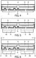
Fig. 1 is a cross-sectional view of a portion of a patterned sapphire substrate having LED layers epitaxially grown over the patterned surface.Fig. 2 illustrates distributed metal contacts making ohmic contact to the p and n-type LED layers.Fig. 3 illustrates a planar stress-buffer layer deposited over the distributed metal contacts and patterned to expose portions of the distributed metal contacts. An optional passivation layer is also shown between the stress-buffer layer and the distributed metal contacts for creating a seal and blocking migration of metal atoms from the subsequently formed metal solder pads.Fig. 4 illustrates relatively thick metal solder pads plated over the planar stress-buffer layer and exposed portions of the distributed metal contacts.Fig. 5 illustrates solder bumps deposited on the metal solder pads.Fig. 6 illustrates the substrate being singulated by laser scribing and breaking.Fig. 7 illustrates a single LED after being singulated using the singulation method ofFig. 6 . The optional passivation layer is eliminated inFig. 7 .Fig. 8 illustrates a single LED, with the metal layers simplified, after being singulated using a combination of mechanical sawing (for the sapphire substrate) and scribing and breaking (for the LED layers), resulting in the edges of the substrate being roughened and the substrate narrowed.- Elements that are the same or similar are labeled with the same numeral.
Figs. 1-8 illustrate a wafer-level process flow in accordance with one embodiment of the invention. Only a single LED area on a much larger wafer is shown for simplicity. Each step shown for an illustrated LED area is applied to all of the LED areas on the large wafer.- With reference to
Fig. 1 , the process flow to create a wafer of LEDs starts with a patterned sapphire substrate (PSS) 10. Thesubstrate 10 will typically have a disc shape and be substantially transparent to the light emitted by the LED. Onesurface 12 is roughened (patterned) such as by grinding, "sand" blasting, chemical etching, plasma etching, or other roughening process. The roughening improves light extraction by reducing total internal reflection (TIR). Thesubstrate 10surface 12 may be patterned in any orderly or random fashion to improve light extraction. - Roughening the semiconductor layer light emitting surface of a conventional flip-chip LED, after removal of the sapphire substrate, is commonly performed. In contrast, the present process retains the sapphire substrate and roughens its growth surface.
- In one embodiment, conventional GaN-based semiconductor LED layers are then epitaxially grown over the roughened
surface 12 of thesubstrate 10. In one embodiment, n-type layers 14 are grown over thesurface 12, followed by anactive layer 16 and p-type layers 18. In one embodiment, theactive layer 16 produces blue light when the LED is energized. - For simplicity, the various semiconductor LED layers are shown as a
single LED layer 20 in the remaining figures. - In
Fig. 2 , a standard process flow is performed to form the thin metal ohmic contacts. A thinreflective metal layer 22, such as silver, nickel, or an alloy, or multiple layers, is deposited on the surface of the p-type layer, such as by sputtering, and patterned. Themetal layer 22, after annealing, creates an ohmic contact with the p-type layer. - A
metal layer 24 of titanium, tungsten, or any alloy is then deposited over themetal layer 22 and patterned. Themetal layer 24 improves adhesion to a subsequent metal layer. Thelayer 24 may also serve as a barrier layer to block the migration of atoms across layers. Themetal layer 24 may be referred to as an interface layer. The thickness of the combination ofmetal layers - The
LED layer 20 is etched atlocations 26 to remove portions of the p-type layers and active layer to expose the n-type layer. - A
dielectric layer 28 is then deposited over the surface and into the openings atlocations 26.Dielectric layer 28 is then patterned to expose portions of themetal layer 24 and to expose the n-type layers atlocations 26. - A
thicker metal layer 30, such as aluminum, nickel, a titanium-tungsten alloy, copper, gold, or alloys, is then deposited over thedielectric layer 28 and into the openings to ohmically contact the p-type layers and n-type layers. Themetal layer 20 may be stacked layers. Themetal layer 30 is then patterned to separate the p-metal contacts 32 from the n-metal contacts 33. Themetal layer 30 may be a few microns thick. - The above metallization process may be conventional so further details are not required for one skilled in the art.
- The metal connections to the p-type layers and n-type layers can be distributed over the entire LED area to more uniformly distribute the current across the LED. This will provide a substantially uniform light emission from the top surface of the LED.
- The resulting
metal layer 30 is not planar due to themetal layer 30 filling the openings and being etched. If themetal layer 30 were plated to form the metal solder pads, the solder pads would not be planar and uniformly thick. It is desirable to provide planar and uniformly thick solder pads for good electrical and thermal conductivity. - In
Fig. 3 , an optionalthin passivation layer 34, such as PECVD SiNx, is deposited to block aluminum atom migration into the semiconductor layers from a subsequently formed solder pad. Depending on the metals used for thelayers passivation layer 34 may not be needed. Thepassivation layer 34 may also be used for hermetic sealing against any moisture or harsh/corrosive environment. A typical thickness of thepassivation layer 34 may be 0.5-1.5um, and preferably 0.8-1.2um. SiNx is a known barrier layer for moisture, while SiOx (or SiO2) or a SiOx/SiNx mixture may also be used. - Since the
passivation layer 34 is formed by a PECVD process, it will be fairly uniform over the non-planar surface, so its surface will not be planar. - Next, in
Fig. 3 , a stress-buffer-layer (SBL) 36, such as BenzoCycloButene (BCB), is coated onto the surface (e.g., by spin-on coating). TheSBL 36 is a dielectric polymer deposited as a liquid. Therefore, the deposition process forms a planar layer of theSBL 36. Deposition by evaporation may also be used. In one embodiment, the thickness of theSBL layer 36 is 1-3um. - Before the
SBL 36 is cured by heating, theSBL 36 is masked, exposed, and developed to form one or more viaopenings 38, which exposes thepassivation layer 34. Photo-BCB is commercially available and has the properties of a photoresist. TheSBL 36 is then cured. Apassivation layer 34 etch is performed by using theSBL 38 as a masking layer. This exposes the p-metal contact 32 and the n-metal contact 33. - The typical thermal conductivity of
suitable SBL 36 materials, such as BCB, PBO: polybenzoxazole, or PI: polyimide, is about 0.3W/m.K. Since theSBL 36 is thin, this is sufficient for very good thermal conductivity for a 1mm2 die size. Atypical SBL 36 thickness after cure and passivation etch should be a minimum of ∼1um to provide adequate step coverage, which is enough for electrical breakdown strength. - Note that the etch step to etch into the LED layers 20 also creates a trench surrounding each LED area that is at least partially filled with the
SBL 36 andpassivation layer 34 for added protection/sealing of the LED. - In
Fig. 4 , a metal redistribution layer (RDL) is deposited that is patterned to formsolder pads Fig. 4 . The Ni is used as a solder barrier layer and the Au is used as a solder wetting layer. Plating is a well know process for forming thick solder pads. - Alternatively, the RDL can be deposited and patterned using a patterned etch or lift-off approach, with added material/process cost.
- By providing the
SBL 36, the surface is planarized so that the resultingsolder pads 44/45 are fairly flat and uniformly thick to evenly spread heat. Providing flat and uniformlythick solder pads 44/45 improves the electrical and thermal conductivity from the LED layers 20 to the heat sink/substrate that the LED will be ultimately mounted on for operation. At this stage, the wafer can be tested. - The use of the stress-butter (SBL) 36 relieves stress between the
solder pads 44/45 and the underlying layers caused by different CTEs of the materials, reducing the possibility of delamination and reducing the possibility of cracking of brittle layers (e.g. layer 20) at stress concentration points, which may cause failure. For example, thesolder pads 44/45 may expand at a different rate than the underlying material and may either shift with respect to theSBL 36 or deform theSBL 36. However, even with such different CTEs, the contact points between thesolder pads 44/45 and the p-metal contact 32 and n-metal contact 33 are not broken since the stress has been relieved by theSBL 36. If theSBL 36 was not planar (flat and smooth), the lateral adhesion of thesolder pads 44/45 to theSBL 36 would be much greater, reducing the effectiveness of theSBL 36. For someSBL 36 materials, such as BCB, theSBL 36 may be hard cured or soft cured to retain a target elasticity so as to deform without delaminating from thesolder pads 44/45 in the event of different expansions of the materials. Thepolymer SBL 36 will typically be more elastic than a non-polymer silicon dioxide oxide layer or a silicon nitride layer typically used as a dielectric. - As previously mentioned, the
SBL 36 also improves the quality of thesolder pads 44/45 by providing a planarized surface, and theSBL 36 also adds a barrier layer for reducing contamination. TheSBL 36 is very thin and is a fairly good conductor of heat, so thermal conduction between the LED and the heat sink is not significantly reduced by theSBL 36. - An optimized design or layout provides optimized thermal performance. For instance, a very good thermal resistance Rth from the metal/semiconductor junction to the solder bumps 48A and 48B (
Fig. 5 ) of 2K/W has been achieved for a 1mm2 die. - As shown in
Fig. 5 , solder bumps 48A and 48B may then be deposited on thesolder pads solder pads 44/45. The thickness range of the solder bumps 48A and 48B can be 1-100um, and preferably 5-10um. The solder bumps 48A and 48B may be Au, AuSn, or any other suitable metal or alloy. - The
sapphire substrate 10 may be thinned at this stage and provided with a desired surface texture, such as by grinding and/or blasting, to reduce the LED height and improve light output. Thetarget substrate 10 thickness can vary depending upon die size, such as from 10 to 1000um, and preferably 200-400um. The suitability of thicknesses of 100-400um has been successfully demonstrated using a conventional back-grinding procedure (wafer mounted on a tape film or a frame) without the need for a wafer support system. However, for a target sapphire thickness of less than 100um, a wafer-support system may be needed to avoid breakage/cracking during grinding. - Finally, as shown in
Fig. 6 , the wafer is singulated into individual LEDs (dice). This has been conducted by laser scribe and break for sapphire thicknesses of 80-300 with die sizes of 0.7-1.4mm in side-length with excellent scribe and break yield loss of <<0.5%. The laser scribe of thesubstrate 10 is represented by theblades 52, and the break lines are represented by the dashed lines 54. The edges of the singulated LEDs are relatively precise and vertical. - By retaining the
sapphire substrate 10 on the final LED, processing cost is saved by not having to remove thesubstrate 10. Yield is also increased. - In case a much thicker (e.g., >400um)
sapphire substrate 10 is needed, a combination of mechanical sawing and laser scribe and break works well, but at a reduced throughput due to the slow sawing speed (typically ∼1mm/s for minimized chipping). Fig. 7 illustrates the singulated LED without the optional passivation layer 34 (compare withFig. 3 ).Fig. 8 illustrates a simplified LED after being singulated by a combination of mechanical sawing of thesubstrate 10 and laser scribe and break of theLED layer 20. As a result, the sapphire side of the die is narrowed on each side (by half the width of the saw blade) so that theLED layer 20 extends beyond thesubstrate 10. This may be advantageous if the substrate 10 (the light emitting surface) is later coated with a phosphor since the sides will be coated. Also, the rough edges of thesubstrate 10 may improve light extraction.- In one embodiment, the singulated LEDs are mounted on a submount wafer by bonding the LED solder pads to pads on the top surface of the submount wafer. A pick and place machine positions the LEDs on the submount, followed by a heating step or an ultrasonic bonding step to bond the LED solder pads to the submount pads. The LEDs are then further processed on a wafer scale, such as being individually encapsulated by a molded silicone lens and/or covered with a phosphor (before or after encapsulation by the lens). The lens material itself may also be infused with phosphor powder. The phosphor may, for example, convert the blue LED light to white light. The submount wafer is then singulated. The submount has robust solder pads on its bottom surface that are electrically connected with vias to the LED solder pads. Alternatively, the LEDs may be directly mounted on printed circuit boards.
- A final cumulative yield after die-attach, phosphor deposition, and dome-lens build has been >99%.
- While particular embodiments of the present invention have been shown and described, it will be obvious to those skilled in the art that changes and modifications may be made without departing from this invention in its broader aspects and, therefore, the appended claims define the scope of this invention.
Claims (13)
- A light emitting device comprising:a transparent growth substrate (10);light emitting diode (LED) layers (20) disposed on the substrate, the LED layers including a p-type layer (18) and an n-type layer (14), the n-type layer (14) being between the p-type layer (18) and the growth substrate (10);wherein the LED layers are etched (26) to expose the n-type layer for electrically connecting to an n-metal contact (33), wherein the etch also creates a trench (26) surrounding the device;one or more metal contact layers (22, 24, 30) electrically contacting the p-type layer and the n-type layer to form the p-metal contact (32) and the n-metal contact (33);a first dielectric layer (28) formed between the p-type layer and the p-metal contact, between the p-type layer and the n-metal contact and also formed in the trench, wherein the first dielectric layer (28) is patterned to expose the n-type layer (14) and to expose the p-type layer (18);a dielectric polymer stress-buffer layer (36) disposed over the p-metal contact (32) and the n-metal contact (33), the stress-buffer layer forming a planar surface over the p-metal contact (32) and the n-metal contact (33), the stress-buffer layer having two or more openings (38) exposing a portion of the p-metal contact (32) and a portion of the n-metal contact (33), wherein the stress-buffer layer at least partially fills the trench (26); andmetal solder pads (44, 45) disposed over the stress-buffer layer (36), wherein the metal solder pads are electrically connected to the p-metal contact (32) and the n-metal contact (33) through the openings (38) in the stress-buffer layer (36),characterized in that,the n-metal contact (33) is deposited into the trench (26) over the patterned first dielectric layer and contacts the n-type layer in the trench.
- The device of Claim 1 wherein the stress-buffer layer (36) is elastic so as to deform when the metal solder pads (44, 45) expand at a different rate than their underlying materials when heat is applied.
- The device of Claim 1 wherein the stress-buffer layer (36) comprises BenzoCycloButene (BCB).
- The device of Claim 1 wherein the growth substrate (10) has a growth surface on which the LED layers are epitaxially grown, wherein the growth surface is patterned (12) prior to growing the LED layers (20).
- The device of Claim 1 further comprising a passivation layer (34) between the stress-buffer layer (36) and the p-metal contact (32) and the n-metal contact (33).
- The device of Claim 1 wherein the device is a flip-chip LED.
- The device of Claim 1 further comprising solder bumps on the solder pads.
- The device of Claim 1 wherein the substrate (10) comprises sapphire and the LED is GaN based.
- The device of Claim 1 wherein the one or more metal contact layers comprise a metal contact layer (22) in physical contact with the p-type layer (18), and an interface layer between the contact layer (24) and the solder pads (44, 45).
- The device of Claim 1 wherein the solder pads (44, 45) comprise multiple metal layers.
- A method for forming a light emitting device comprising:epitaxially growing light emitting diode (LED) layers (20) on a transparent growth substrate (10), the LED layers including a p-type layer (18) and an n-type layer (14);etching (26) the LED layers to expose one of the p-type layer and n-type layer for electrically connecting to a p-metal contact (32) or an n-metal contact (33), wherein the etch also creates trench surrounding the device;depositing and patterning one or more metal contact layers (22, 24, 30) electrically contacting the p-type layer and the n-type layer to form the p-metal contact and the n-metal contact;depositing a dielectric polymer stress-buffer layer (36) over the p-metal contact and the n-metal contact, the stress-buffer layer forming a planar surface over the p-metal contact and the n-metal contact, the stress-buffer layer having two or more openings (38) exposing a portion of the p-metal contact and a portion of the n-metal contact; wherein the stress-buffer layer at least partially fills the trench; andforming metal solder pads (44, 45) over the stress-buffer layer, the metal solder pads electrically contacting the p-metal contact and the n-metal contact through the openings in the stress-buffer layer,characterized in that,the n-metal contact (33) is deposited into the trench (26) over the patterned first dielectric layer and contacts the n-type layer in the trench.
- The method of Claim 11 wherein the stress-buffer layer (36) is elastic so as to deform when the metal solder pads (44, 45) expand at a different rate than their underlying materials when heat is applied.
- The method of Claim 11 wherein the stress-buffer layer (36) comprises BenzoCycloButene (BCB).
Applications Claiming Priority (2)
| Application Number | Priority Date | Filing Date | Title |
|---|---|---|---|
| US201361842431P | 2013-07-03 | 2013-07-03 | |
| PCT/IB2014/062535WO2015001446A1 (en) | 2013-07-03 | 2014-06-23 | Led with stress-buffer layer under metallization layer |
Publications (2)
| Publication Number | Publication Date |
|---|---|
| EP3017483A1 EP3017483A1 (en) | 2016-05-11 |
| EP3017483B1true EP3017483B1 (en) | 2020-05-06 |
Family
ID=51211278
Family Applications (1)
| Application Number | Title | Priority Date | Filing Date |
|---|---|---|---|
| EP14741393.4AActiveEP3017483B1 (en) | 2013-07-03 | 2014-06-23 | Led with stress-buffer layer under metallization layer |
Country Status (7)
| Country | Link |
|---|---|
| US (2) | US9640729B2 (en) |
| EP (1) | EP3017483B1 (en) |
| JP (2) | JP2016526797A (en) |
| KR (1) | KR102235020B1 (en) |
| CN (1) | CN105340089B (en) |
| TW (1) | TWI629808B (en) |
| WO (1) | WO2015001446A1 (en) |
Families Citing this family (14)
| Publication number | Priority date | Publication date | Assignee | Title |
|---|---|---|---|---|
| KR102407827B1 (en)* | 2015-01-27 | 2022-06-13 | 서울바이오시스 주식회사 | Light emitting device |
| US9543488B2 (en) | 2014-06-23 | 2017-01-10 | Seoul Viosys Co., Ltd. | Light emitting device |
| KR102323536B1 (en)* | 2015-01-19 | 2021-11-09 | 서울바이오시스 주식회사 | Light emitting device |
| KR102347487B1 (en)* | 2015-03-16 | 2022-01-07 | 서울바이오시스 주식회사 | Light-emitting diode including metal bulk |
| TWI772253B (en) | 2015-11-13 | 2022-08-01 | 晶元光電股份有限公司 | Light-emitting device |
| DE102017104144B9 (en)* | 2017-02-28 | 2022-03-10 | OSRAM Opto Semiconductors Gesellschaft mit beschränkter Haftung | Process for the production of light-emitting diodes |
| TWI647835B (en) | 2017-07-05 | 2019-01-11 | 英屬開曼群島商錼創科技股份有限公司 | Display panel |
| CN109216285B (en)* | 2017-07-05 | 2022-01-25 | 英属开曼群岛商錼创科技股份有限公司 | display panel |
| US11024770B2 (en) | 2017-09-25 | 2021-06-01 | Nichia Corporation | Light emitting element and light emitting device |
| JP7055201B2 (en) | 2018-06-08 | 2022-04-15 | 日機装株式会社 | Semiconductor light emitting device |
| DE102018118824A1 (en) | 2018-08-02 | 2020-02-06 | Osram Opto Semiconductors Gmbh | SEMICONDUCTOR COMPONENT WITH A STRESS COMPENSATION LAYER AND METHOD FOR PRODUCING A SEMICONDUCTOR COMPONENT |
| GB2593698B (en)* | 2020-03-30 | 2022-12-07 | Plessey Semiconductors Ltd | Monolithic electronic device |
| CN114944444A (en)* | 2022-05-09 | 2022-08-26 | 厦门乾照光电股份有限公司 | Micro-light-emitting device based on tin alloy electrode application and preparation method thereof |
| US20240371803A1 (en)* | 2023-05-01 | 2024-11-07 | Taiwan Semiconductor Manufacturing Company, Ltd. | Method for forming a redistribution layer structure, and chip package structure |
Citations (2)
| Publication number | Priority date | Publication date | Assignee | Title |
|---|---|---|---|---|
| US6614056B1 (en)* | 1999-12-01 | 2003-09-02 | Cree Lighting Company | Scalable led with improved current spreading structures |
| JP2013089667A (en)* | 2011-10-14 | 2013-05-13 | Citizen Holdings Co Ltd | Semiconductor light-emitting element |
Family Cites Families (47)
| Publication number | Priority date | Publication date | Assignee | Title |
|---|---|---|---|---|
| JPS57190341A (en)* | 1981-05-19 | 1982-11-22 | Citizen Watch Co Ltd | Circuit borad composition |
| JPH06349892A (en)* | 1993-06-10 | 1994-12-22 | Matsushita Electric Ind Co Ltd | Method for manufacturing semiconductor device |
| US6075290A (en)* | 1998-02-26 | 2000-06-13 | National Semiconductor Corporation | Surface mount die: wafer level chip-scale package and process for making the same |
| JP2001217461A (en)* | 2000-02-04 | 2001-08-10 | Matsushita Electric Ind Co Ltd | Composite light emitting device |
| JP3328647B2 (en)* | 2000-08-22 | 2002-09-30 | サンユレック株式会社 | Optoelectronic component manufacturing method |
| JP2004103975A (en)* | 2002-09-12 | 2004-04-02 | Citizen Watch Co Ltd | Optical semiconductor element, method for manufacturing the same, and optical semiconductor device mounting optical semiconductor element |
| WO2005017962A2 (en)* | 2003-08-04 | 2005-02-24 | Nanosys, Inc. | System and process for producing nanowire composites and electronic substrates therefrom |
| KR100595884B1 (en)* | 2004-05-18 | 2006-07-03 | 엘지전자 주식회사 | Nitride semiconductor device manufacturing method |
| JP2006228855A (en)* | 2005-02-16 | 2006-08-31 | Rohm Co Ltd | Semiconductor light emitting device and manufacturing method thereof |
| JP4956902B2 (en)* | 2005-03-18 | 2012-06-20 | 三菱化学株式会社 | GaN-based light emitting diode and light emitting device using the same |
| TWI273667B (en)* | 2005-08-30 | 2007-02-11 | Via Tech Inc | Chip package and bump connecting structure thereof |
| SG149807A1 (en)* | 2007-07-30 | 2009-02-27 | Stats Chippac Ltd | Semiconductor device and method of providing common voltage bus and wire bondable redistribution |
| JP5150367B2 (en)* | 2008-05-27 | 2013-02-20 | 東芝ディスクリートテクノロジー株式会社 | Light emitting device and manufacturing method thereof |
| US8124999B2 (en) | 2008-07-18 | 2012-02-28 | Toyoda Gosei Co., Ltd. | Light emitting element and method of making the same |
| JP5151758B2 (en)* | 2008-07-18 | 2013-02-27 | 豊田合成株式会社 | Light emitting element |
| JP4799606B2 (en)* | 2008-12-08 | 2011-10-26 | 株式会社東芝 | Optical semiconductor device and method for manufacturing optical semiconductor device |
| JP4724222B2 (en)* | 2008-12-12 | 2011-07-13 | 株式会社東芝 | Method for manufacturing light emitting device |
| US20100193950A1 (en)* | 2009-01-30 | 2010-08-05 | E.I.Du Pont De Nemours And Company | Wafer level, chip scale semiconductor device packaging compositions, and methods relating thereto |
| US7732231B1 (en) | 2009-06-03 | 2010-06-08 | Philips Lumileds Lighting Company, Llc | Method of forming a dielectric layer on a semiconductor light emitting device |
| US7989824B2 (en)* | 2009-06-03 | 2011-08-02 | Koninklijke Philips Electronics N.V. | Method of forming a dielectric layer on a semiconductor light emitting device |
| JP2011040632A (en)* | 2009-08-13 | 2011-02-24 | Sumitomo Electric Ind Ltd | Semiconductor optical element |
| KR20170102364A (en) | 2009-09-07 | 2017-09-08 | 엘시드 가부시끼가이샤 | Semiconductor light emitting element |
| JP2011091374A (en) | 2009-09-11 | 2011-05-06 | Samco Inc | Method of etching sapphire substrate |
| JP2011071272A (en)* | 2009-09-25 | 2011-04-07 | Toshiba Corp | Semiconductor light-emitting device and method for manufacturing the same |
| JP5349260B2 (en)* | 2009-11-19 | 2013-11-20 | 株式会社東芝 | Semiconductor light emitting device and manufacturing method thereof |
| JP2011138913A (en)* | 2009-12-28 | 2011-07-14 | Citizen Holdings Co Ltd | Semiconductor light-emitting element and method for manufacturing the same |
| US8354750B2 (en)* | 2010-02-01 | 2013-01-15 | Taiwan Semiconductor Manufacturing Company, Ltd. | Stress buffer structures in a mounting structure of a semiconductor device |
| JP5017399B2 (en)* | 2010-03-09 | 2012-09-05 | 株式会社東芝 | Semiconductor light emitting device and method for manufacturing semiconductor light emitting device |
| JP2011199193A (en)* | 2010-03-23 | 2011-10-06 | Toshiba Corp | Light emitting device and method of manufacturing the same |
| JP2011233650A (en)* | 2010-04-26 | 2011-11-17 | Toshiba Corp | Semiconductor light-emitting device |
| JP5353809B2 (en)* | 2010-05-10 | 2013-11-27 | 豊田合成株式会社 | Semiconductor light emitting element and light emitting device |
| JP5325834B2 (en)* | 2010-05-24 | 2013-10-23 | 株式会社東芝 | Semiconductor light emitting device and manufacturing method thereof |
| US8283781B2 (en)* | 2010-09-10 | 2012-10-09 | Taiwan Semiconductor Manufacturing Company, Ltd. | Semiconductor device having pad structure with stress buffer layer |
| KR20120077876A (en)* | 2010-12-31 | 2012-07-10 | 삼성전자주식회사 | Heterojunction structures of different substrates joined and methods for fabricating the same |
| JP5582054B2 (en)* | 2011-02-09 | 2014-09-03 | 豊田合成株式会社 | Semiconductor light emitting device |
| JP5603813B2 (en)* | 2011-03-15 | 2014-10-08 | 株式会社東芝 | Semiconductor light emitting device and light emitting device |
| JP5535114B2 (en) | 2011-03-25 | 2014-07-02 | 株式会社東芝 | Light emitting device, light emitting module, and method of manufacturing light emitting device |
| JP5642623B2 (en) | 2011-05-17 | 2014-12-17 | 株式会社東芝 | Semiconductor light emitting device |
| KR101262509B1 (en)* | 2011-05-27 | 2013-05-08 | 엘지이노텍 주식회사 | Light emitting device, light emitting module and fabricating method for light emitting device |
| US9269878B2 (en)* | 2011-05-27 | 2016-02-23 | Lg Innotek Co., Ltd. | Light emitting device and light emitting apparatus |
| US8883634B2 (en)* | 2011-06-29 | 2014-11-11 | Globalfoundries Singapore Pte. Ltd. | Package interconnects |
| US9343612B2 (en)* | 2011-07-15 | 2016-05-17 | Koninklijke Philips N.V. | Method of bonding a semiconductor device to a support substrate |
| JP5662277B2 (en)* | 2011-08-08 | 2015-01-28 | 株式会社東芝 | Semiconductor light emitting device and light emitting module |
| WO2013050898A1 (en)* | 2011-10-07 | 2013-04-11 | Koninklijke Philips Electronics N.V. | Electrically insulating bond for mounting a light emitting device |
| WO2013084103A1 (en) | 2011-12-08 | 2013-06-13 | Koninklijke Philips Electronics N.V. | Semiconductor light emitting device with thick metal layers |
| EP2748865B1 (en)* | 2011-12-08 | 2019-04-10 | Lumileds Holding B.V. | Semiconductor light emitting device with thick metal layers |
| KR20140108546A (en)* | 2011-12-08 | 2014-09-11 | 코닌클리케 필립스 엔.브이. | Semiconductor light emitting device with thick metal layers |
- 2014
- 2014-06-23EPEP14741393.4Apatent/EP3017483B1/enactiveActive
- 2014-06-23CNCN201480037882.7Apatent/CN105340089B/enactiveActive
- 2014-06-23WOPCT/IB2014/062535patent/WO2015001446A1/enactiveApplication Filing
- 2014-06-23KRKR1020167002960Apatent/KR102235020B1/enactiveActive
- 2014-06-23JPJP2016522922Apatent/JP2016526797A/enactivePending
- 2014-06-23USUS14/902,001patent/US9640729B2/enactiveActive
- 2014-07-03TWTW103123043Apatent/TWI629808B/enactive
- 2017
- 2017-04-28USUS15/581,204patent/US10050180B2/enactiveActive
- 2018
- 2018-12-07JPJP2018229848Apatent/JP6745323B2/enactiveActive
Patent Citations (2)
| Publication number | Priority date | Publication date | Assignee | Title |
|---|---|---|---|---|
| US6614056B1 (en)* | 1999-12-01 | 2003-09-02 | Cree Lighting Company | Scalable led with improved current spreading structures |
| JP2013089667A (en)* | 2011-10-14 | 2013-05-13 | Citizen Holdings Co Ltd | Semiconductor light-emitting element |
Also Published As
| Publication number | Publication date |
|---|---|
| EP3017483A1 (en) | 2016-05-11 |
| CN105340089A (en) | 2016-02-17 |
| JP2019062224A (en) | 2019-04-18 |
| CN105340089B (en) | 2021-03-12 |
| US20160329468A1 (en) | 2016-11-10 |
| KR20160029104A (en) | 2016-03-14 |
| JP6745323B2 (en) | 2020-08-26 |
| WO2015001446A1 (en) | 2015-01-08 |
| TW201511367A (en) | 2015-03-16 |
| JP2016526797A (en) | 2016-09-05 |
| US9640729B2 (en) | 2017-05-02 |
| KR102235020B1 (en) | 2021-04-02 |
| TWI629808B (en) | 2018-07-11 |
| US10050180B2 (en) | 2018-08-14 |
| US20170358715A1 (en) | 2017-12-14 |
Similar Documents
| Publication | Publication Date | Title |
|---|---|---|
| US10050180B2 (en) | LED with stress-buffer layer under metallization layer | |
| US10170675B2 (en) | P—N separation metal fill for flip chip LEDs | |
| US8384118B2 (en) | LED assembly having maximum metal support for laser lift-off of growth substrate | |
| JP7353770B2 (en) | Semiconductor device with back metal and related method | |
| US9722137B2 (en) | LED having vertical contacts redistributed for flip chip mounting | |
| TW201547053A (en) | Method of forming a light emitting device | |
| EP2427923B1 (en) | Extension of contact pads to the die edge with electrical isolation | |
| WO2013057668A1 (en) | Led wafer bonded to carrier wafer for wafer level processing | |
| WO2013050898A1 (en) | Electrically insulating bond for mounting a light emitting device | |
| WO2013021305A1 (en) | Wafer level processing of leds using carrier wafer |
Legal Events
| Date | Code | Title | Description |
|---|---|---|---|
| PUAI | Public reference made under article 153(3) epc to a published international application that has entered the european phase | Free format text:ORIGINAL CODE: 0009012 | |
| 17P | Request for examination filed | Effective date:20160203 | |
| AK | Designated contracting states | Kind code of ref document:A1 Designated state(s):AL AT BE BG CH CY CZ DE DK EE ES FI FR GB GR HR HU IE IS IT LI LT LU LV MC MK MT NL NO PL PT RO RS SE SI SK SM TR | |
| AX | Request for extension of the european patent | Extension state:BA ME | |
| DAX | Request for extension of the european patent (deleted) | ||
| STAA | Information on the status of an ep patent application or granted ep patent | Free format text:STATUS: EXAMINATION IS IN PROGRESS | |
| 17Q | First examination report despatched | Effective date:20170825 | |
| RAP1 | Party data changed (applicant data changed or rights of an application transferred) | Owner name:LUMILEDS HOLDING B.V. | |
| RAP1 | Party data changed (applicant data changed or rights of an application transferred) | Owner name:LUMILEDS HOLDING B.V. | |
| GRAP | Despatch of communication of intention to grant a patent | Free format text:ORIGINAL CODE: EPIDOSNIGR1 | |
| STAA | Information on the status of an ep patent application or granted ep patent | Free format text:STATUS: GRANT OF PATENT IS INTENDED | |
| INTG | Intention to grant announced | Effective date:20200122 | |
| GRAS | Grant fee paid | Free format text:ORIGINAL CODE: EPIDOSNIGR3 | |
| GRAA | (expected) grant | Free format text:ORIGINAL CODE: 0009210 | |
| STAA | Information on the status of an ep patent application or granted ep patent | Free format text:STATUS: THE PATENT HAS BEEN GRANTED | |
| AK | Designated contracting states | Kind code of ref document:B1 Designated state(s):AL AT BE BG CH CY CZ DE DK EE ES FI FR GB GR HR HU IE IS IT LI LT LU LV MC MK MT NL NO PL PT RO RS SE SI SK SM TR | |
| REG | Reference to a national code | Ref country code:GB Ref legal event code:FG4D | |
| REG | Reference to a national code | Ref country code:CH Ref legal event code:EP Ref country code:AT Ref legal event code:REF Ref document number:1268245 Country of ref document:AT Kind code of ref document:T Effective date:20200515 | |
| REG | Reference to a national code | Ref country code:IE Ref legal event code:FG4D | |
| REG | Reference to a national code | Ref country code:DE Ref legal event code:R096 Ref document number:602014064973 Country of ref document:DE | |
| REG | Reference to a national code | Ref country code:LT Ref legal event code:MG4D | |
| REG | Reference to a national code | Ref country code:NL Ref legal event code:MP Effective date:20200506 | |
| PG25 | Lapsed in a contracting state [announced via postgrant information from national office to epo] | Ref country code:SE Free format text:LAPSE BECAUSE OF FAILURE TO SUBMIT A TRANSLATION OF THE DESCRIPTION OR TO PAY THE FEE WITHIN THE PRESCRIBED TIME-LIMIT Effective date:20200506 Ref country code:FI Free format text:LAPSE BECAUSE OF FAILURE TO SUBMIT A TRANSLATION OF THE DESCRIPTION OR TO PAY THE FEE WITHIN THE PRESCRIBED TIME-LIMIT Effective date:20200506 Ref country code:PT Free format text:LAPSE BECAUSE OF FAILURE TO SUBMIT A TRANSLATION OF THE DESCRIPTION OR TO PAY THE FEE WITHIN THE PRESCRIBED TIME-LIMIT Effective date:20200907 Ref country code:IS Free format text:LAPSE BECAUSE OF FAILURE TO SUBMIT A TRANSLATION OF THE DESCRIPTION OR TO PAY THE FEE WITHIN THE PRESCRIBED TIME-LIMIT Effective date:20200906 Ref country code:GR Free format text:LAPSE BECAUSE OF FAILURE TO SUBMIT A TRANSLATION OF THE DESCRIPTION OR TO PAY THE FEE WITHIN THE PRESCRIBED TIME-LIMIT Effective date:20200807 Ref country code:NO Free format text:LAPSE BECAUSE OF FAILURE TO SUBMIT A TRANSLATION OF THE DESCRIPTION OR TO PAY THE FEE WITHIN THE PRESCRIBED TIME-LIMIT Effective date:20200806 Ref country code:LT Free format text:LAPSE BECAUSE OF FAILURE TO SUBMIT A TRANSLATION OF THE DESCRIPTION OR TO PAY THE FEE WITHIN THE PRESCRIBED TIME-LIMIT Effective date:20200506 | |
| PG25 | Lapsed in a contracting state [announced via postgrant information from national office to epo] | Ref country code:LV Free format text:LAPSE BECAUSE OF FAILURE TO SUBMIT A TRANSLATION OF THE DESCRIPTION OR TO PAY THE FEE WITHIN THE PRESCRIBED TIME-LIMIT Effective date:20200506 Ref country code:RS Free format text:LAPSE BECAUSE OF FAILURE TO SUBMIT A TRANSLATION OF THE DESCRIPTION OR TO PAY THE FEE WITHIN THE PRESCRIBED TIME-LIMIT Effective date:20200506 Ref country code:BG Free format text:LAPSE BECAUSE OF FAILURE TO SUBMIT A TRANSLATION OF THE DESCRIPTION OR TO PAY THE FEE WITHIN THE PRESCRIBED TIME-LIMIT Effective date:20200806 Ref country code:HR Free format text:LAPSE BECAUSE OF FAILURE TO SUBMIT A TRANSLATION OF THE DESCRIPTION OR TO PAY THE FEE WITHIN THE PRESCRIBED TIME-LIMIT Effective date:20200506 | |
| REG | Reference to a national code | Ref country code:AT Ref legal event code:MK05 Ref document number:1268245 Country of ref document:AT Kind code of ref document:T Effective date:20200506 | |
| PG25 | Lapsed in a contracting state [announced via postgrant information from national office to epo] | Ref country code:NL Free format text:LAPSE BECAUSE OF FAILURE TO SUBMIT A TRANSLATION OF THE DESCRIPTION OR TO PAY THE FEE WITHIN THE PRESCRIBED TIME-LIMIT Effective date:20200506 Ref country code:AL Free format text:LAPSE BECAUSE OF FAILURE TO SUBMIT A TRANSLATION OF THE DESCRIPTION OR TO PAY THE FEE WITHIN THE PRESCRIBED TIME-LIMIT Effective date:20200506 | |
| PG25 | Lapsed in a contracting state [announced via postgrant information from national office to epo] | Ref country code:CZ Free format text:LAPSE BECAUSE OF FAILURE TO SUBMIT A TRANSLATION OF THE DESCRIPTION OR TO PAY THE FEE WITHIN THE PRESCRIBED TIME-LIMIT Effective date:20200506 Ref country code:RO Free format text:LAPSE BECAUSE OF FAILURE TO SUBMIT A TRANSLATION OF THE DESCRIPTION OR TO PAY THE FEE WITHIN THE PRESCRIBED TIME-LIMIT Effective date:20200506 Ref country code:SM Free format text:LAPSE BECAUSE OF FAILURE TO SUBMIT A TRANSLATION OF THE DESCRIPTION OR TO PAY THE FEE WITHIN THE PRESCRIBED TIME-LIMIT Effective date:20200506 Ref country code:EE Free format text:LAPSE BECAUSE OF FAILURE TO SUBMIT A TRANSLATION OF THE DESCRIPTION OR TO PAY THE FEE WITHIN THE PRESCRIBED TIME-LIMIT Effective date:20200506 Ref country code:DK Free format text:LAPSE BECAUSE OF FAILURE TO SUBMIT A TRANSLATION OF THE DESCRIPTION OR TO PAY THE FEE WITHIN THE PRESCRIBED TIME-LIMIT Effective date:20200506 Ref country code:IT Free format text:LAPSE BECAUSE OF FAILURE TO SUBMIT A TRANSLATION OF THE DESCRIPTION OR TO PAY THE FEE WITHIN THE PRESCRIBED TIME-LIMIT Effective date:20200506 Ref country code:AT Free format text:LAPSE BECAUSE OF FAILURE TO SUBMIT A TRANSLATION OF THE DESCRIPTION OR TO PAY THE FEE WITHIN THE PRESCRIBED TIME-LIMIT Effective date:20200506 Ref country code:ES Free format text:LAPSE BECAUSE OF FAILURE TO SUBMIT A TRANSLATION OF THE DESCRIPTION OR TO PAY THE FEE WITHIN THE PRESCRIBED TIME-LIMIT Effective date:20200506 | |
| REG | Reference to a national code | Ref country code:CH Ref legal event code:PL | |
| REG | Reference to a national code | Ref country code:DE Ref legal event code:R097 Ref document number:602014064973 Country of ref document:DE | |
| PG25 | Lapsed in a contracting state [announced via postgrant information from national office to epo] | Ref country code:SK Free format text:LAPSE BECAUSE OF FAILURE TO SUBMIT A TRANSLATION OF THE DESCRIPTION OR TO PAY THE FEE WITHIN THE PRESCRIBED TIME-LIMIT Effective date:20200506 Ref country code:PL Free format text:LAPSE BECAUSE OF FAILURE TO SUBMIT A TRANSLATION OF THE DESCRIPTION OR TO PAY THE FEE WITHIN THE PRESCRIBED TIME-LIMIT Effective date:20200506 Ref country code:MC Free format text:LAPSE BECAUSE OF FAILURE TO SUBMIT A TRANSLATION OF THE DESCRIPTION OR TO PAY THE FEE WITHIN THE PRESCRIBED TIME-LIMIT Effective date:20200506 | |
| PLBE | No opposition filed within time limit | Free format text:ORIGINAL CODE: 0009261 | |
| STAA | Information on the status of an ep patent application or granted ep patent | Free format text:STATUS: NO OPPOSITION FILED WITHIN TIME LIMIT | |
| PG25 | Lapsed in a contracting state [announced via postgrant information from national office to epo] | Ref country code:LU Free format text:LAPSE BECAUSE OF NON-PAYMENT OF DUE FEES Effective date:20200623 | |
| 26N | No opposition filed | Effective date:20210209 | |
| REG | Reference to a national code | Ref country code:BE Ref legal event code:MM Effective date:20200630 | |
| PG25 | Lapsed in a contracting state [announced via postgrant information from national office to epo] | Ref country code:LI Free format text:LAPSE BECAUSE OF NON-PAYMENT OF DUE FEES Effective date:20200630 Ref country code:IE Free format text:LAPSE BECAUSE OF NON-PAYMENT OF DUE FEES Effective date:20200623 Ref country code:CH Free format text:LAPSE BECAUSE OF NON-PAYMENT OF DUE FEES Effective date:20200630 | |
| PG25 | Lapsed in a contracting state [announced via postgrant information from national office to epo] | Ref country code:BE Free format text:LAPSE BECAUSE OF NON-PAYMENT OF DUE FEES Effective date:20200630 Ref country code:SI Free format text:LAPSE BECAUSE OF FAILURE TO SUBMIT A TRANSLATION OF THE DESCRIPTION OR TO PAY THE FEE WITHIN THE PRESCRIBED TIME-LIMIT Effective date:20200506 | |
| PG25 | Lapsed in a contracting state [announced via postgrant information from national office to epo] | Ref country code:TR Free format text:LAPSE BECAUSE OF FAILURE TO SUBMIT A TRANSLATION OF THE DESCRIPTION OR TO PAY THE FEE WITHIN THE PRESCRIBED TIME-LIMIT Effective date:20200506 Ref country code:MT Free format text:LAPSE BECAUSE OF FAILURE TO SUBMIT A TRANSLATION OF THE DESCRIPTION OR TO PAY THE FEE WITHIN THE PRESCRIBED TIME-LIMIT Effective date:20200506 Ref country code:CY Free format text:LAPSE BECAUSE OF FAILURE TO SUBMIT A TRANSLATION OF THE DESCRIPTION OR TO PAY THE FEE WITHIN THE PRESCRIBED TIME-LIMIT Effective date:20200506 | |
| PG25 | Lapsed in a contracting state [announced via postgrant information from national office to epo] | Ref country code:MK Free format text:LAPSE BECAUSE OF FAILURE TO SUBMIT A TRANSLATION OF THE DESCRIPTION OR TO PAY THE FEE WITHIN THE PRESCRIBED TIME-LIMIT Effective date:20200506 | |
| P01 | Opt-out of the competence of the unified patent court (upc) registered | Effective date:20230530 | |
| REG | Reference to a national code | Ref country code:DE Ref legal event code:R079 Ref document number:602014064973 Country of ref document:DE Free format text:PREVIOUS MAIN CLASS: H01L0033440000 Ipc:H10H0020840000 | |
| PGFP | Annual fee paid to national office [announced via postgrant information from national office to epo] | Ref country code:DE Payment date:20250626 Year of fee payment:12 | |
| PGFP | Annual fee paid to national office [announced via postgrant information from national office to epo] | Ref country code:GB Payment date:20250617 Year of fee payment:12 | |
| PGFP | Annual fee paid to national office [announced via postgrant information from national office to epo] | Ref country code:FR Payment date:20250624 Year of fee payment:12 |