EP3003131B1 - Apparatus for detecting optical signals from implanted sensors - Google Patents
Apparatus for detecting optical signals from implanted sensorsDownload PDFInfo
- Publication number
- EP3003131B1 EP3003131B1EP14807637.5AEP14807637AEP3003131B1EP 3003131 B1EP3003131 B1EP 3003131B1EP 14807637 AEP14807637 AEP 14807637AEP 3003131 B1EP3003131 B1EP 3003131B1
- Authority
- EP
- European Patent Office
- Prior art keywords
- light
- detector
- light source
- excitation
- optical signal
- Prior art date
- Legal status (The legal status is an assumption and is not a legal conclusion. Google has not performed a legal analysis and makes no representation as to the accuracy of the status listed.)
- Active
Links
Images


Classifications
- A—HUMAN NECESSITIES
- A61—MEDICAL OR VETERINARY SCIENCE; HYGIENE
- A61B—DIAGNOSIS; SURGERY; IDENTIFICATION
- A61B5/00—Measuring for diagnostic purposes; Identification of persons
- A61B5/145—Measuring characteristics of blood in vivo, e.g. gas concentration or pH-value ; Measuring characteristics of body fluids or tissues, e.g. interstitial fluid or cerebral tissue
- A61B5/1455—Measuring characteristics of blood in vivo, e.g. gas concentration or pH-value ; Measuring characteristics of body fluids or tissues, e.g. interstitial fluid or cerebral tissue using optical sensors, e.g. spectral photometrical oximeters
- A61B5/1459—Measuring characteristics of blood in vivo, e.g. gas concentration or pH-value ; Measuring characteristics of body fluids or tissues, e.g. interstitial fluid or cerebral tissue using optical sensors, e.g. spectral photometrical oximeters invasive, e.g. introduced into the body by a catheter
- A—HUMAN NECESSITIES
- A61—MEDICAL OR VETERINARY SCIENCE; HYGIENE
- A61B—DIAGNOSIS; SURGERY; IDENTIFICATION
- A61B2562/00—Details of sensors; Constructional details of sensor housings or probes; Accessories for sensors
- A61B2562/02—Details of sensors specially adapted for in-vivo measurements
- A61B2562/0233—Special features of optical sensors or probes classified in A61B5/00
- A—HUMAN NECESSITIES
- A61—MEDICAL OR VETERINARY SCIENCE; HYGIENE
- A61B—DIAGNOSIS; SURGERY; IDENTIFICATION
- A61B2562/00—Details of sensors; Constructional details of sensor housings or probes; Accessories for sensors
- A61B2562/04—Arrangements of multiple sensors of the same type
- A61B2562/043—Arrangements of multiple sensors of the same type in a linear array
- A—HUMAN NECESSITIES
- A61—MEDICAL OR VETERINARY SCIENCE; HYGIENE
- A61B—DIAGNOSIS; SURGERY; IDENTIFICATION
- A61B5/00—Measuring for diagnostic purposes; Identification of persons
- A61B5/0002—Remote monitoring of patients using telemetry, e.g. transmission of vital signals via a communication network
- A61B5/0015—Remote monitoring of patients using telemetry, e.g. transmission of vital signals via a communication network characterised by features of the telemetry system
- A61B5/0017—Remote monitoring of patients using telemetry, e.g. transmission of vital signals via a communication network characterised by features of the telemetry system transmitting optical signals
- A—HUMAN NECESSITIES
- A61—MEDICAL OR VETERINARY SCIENCE; HYGIENE
- A61B—DIAGNOSIS; SURGERY; IDENTIFICATION
- A61B5/00—Measuring for diagnostic purposes; Identification of persons
- A61B5/145—Measuring characteristics of blood in vivo, e.g. gas concentration or pH-value ; Measuring characteristics of body fluids or tissues, e.g. interstitial fluid or cerebral tissue
- A61B5/14532—Measuring characteristics of blood in vivo, e.g. gas concentration or pH-value ; Measuring characteristics of body fluids or tissues, e.g. interstitial fluid or cerebral tissue for measuring glucose, e.g. by tissue impedance measurement
Definitions
- Some embodiments described hereinrelate to apparatus and methods for monitoring an implant, and in particular to apparatus and methods for detecting optical signals emitted from an implant with restriction of off-axis light.
- Some embodiments described hereinrelate to apparatus and methods for monitoring an implant, and in particular to apparatus and methods for detecting optical signals through a relatively large surface area of tissue relative to a surface area of tissue through which an excitation optical signal is supplied.
- the monitoring of the level or concentration of an analyte, such as glucose, lactate, oxygen, etc., in certain individualsis important to their health. High or low levels of glucose, or other analytes, may have detrimental effects or be indicative of specific health states.
- the monitoring of glucoseis particularly important to persons with diabetes, a subset of whom must determine when insulin is needed to reduce glucose levels in their bodies or when additional glucose is needed to raise the level of glucose in their bodies.
- a conventional technique used by many persons with diabetes for monitoring their blood glucose levelincludes the periodic drawing of blood, the application of that blood to a test strip, and the determination of the blood glucose level using calorimetric, electrochemical, or photometric detection. This technique does not permit continuous or automatic monitoring of glucose levels in the body, but typically must be performed manually on a periodic basis. Unfortunately, the consistency with which the level of glucose is checked varies widely among individuals. Many persons with diabetes find the periodic testing inconvenient, and they sometimes forget to test their glucose level or do not have time for a proper test. In addition, some individuals wish to avoid the pain associated with the test. Unmonitored glucose may result in hyperglycemic or hypoglycemic episodes. An implanted sensor that monitors the individual's analyte levels would enable individuals to monitor their glucose, or other analyte levels, more easily.
- Some known devicesperform in situ monitoring of analytes (e.g., glucose) in the blood stream or interstitial fluid of various tissues.
- analytese.g., glucose
- a number of these devicesuse sensors that are inserted into a blood vessel or under the skin of a patient.
- Communicating and/or retrieving data from such known and/or proposed devicescan be challenging.
- an implanted sensormay be able to communicate with a detector or receiver using radio frequency (RF) transmissions.
- RFradio frequency
- Such a sensormay require electronics, batteries, antennae, and/or other communication hardware which may increase the bulk of the implanted sensor, may require frequent inconvenient recharging, and/or may decrease the longevity or reliability of the implant.
- WO 2013/073270discloses a measurement device including a light source for emitting measurement light which is used for measuring an in vivo component present in a living body.
- a fluorescent sensormay not require electric charging and/or transmission electronics.
- Such implanted sensorsmay be difficult to read or to monitor optically because of low levels of florescence in the presence of high scatter due to dynamic changes in skin conditions (e.g., blood level and hydration).
- the skinis highly scattering, and the scattering may dominate the optical propagation. Scatter is caused by index of refraction changes in the tissue, and the main components of scatter in the skin are due to lipids, collagen, and other biological components.
- the main absorptionis caused by blood, melanin, water, and other components.
- Devices and apparatus described hereinare suitable for providing accurate and consistent measurement of an analyte by monitoring an implantable sensor in such low-signal, high-scattering environments.
- an apparatusincluding a light source configured to transmit an excitation optical signal through a first area of skin to an implanted sensor; a plurality of detectors substantially surrounding the light source, the plurality of detectors configured to detect an analyte-dependent optical signal emitted from the implanted sensor through a second surface area of skin in response to the implanted sensor being illuminated by the excitation optical signal, the second surface area of the skin being at least four times the first surface area of the skin; and a lens configured to focus at least a portion of the analyte-dependent optical signal onto the detector.
- Each lens from the array of lensescan be configured to transmit an analyte-dependent optical signal from an implanted sensor to a detector.
- a plurality of light-blocking elementscan be disposed within a substrate of the array of lenses. Each light blocking element from the array of light-blocking elements can be configured to prevent or inhibit a photon having an angle of incidence greater than a predetermined angle of incidence from passing through the substrate.
- Some embodiments described hereinrelate to an apparatus including a detector configured to detect an analyte-dependent optical signal from an implanted sensor.
- a lenscan be configured to focus at least a portion of the analyte-dependent optical signal onto the detector.
- a filtercan be configured to attenuate light having wavelengths shorter than the analyte-dependent optical signal.
- a device including at least one light sourcecan be arranged to transmit the excitation light through tissue surrounding the implant.
- the devicecan include at least one detector arranged to detect light emitted from implanted sensor and transmitted through the tissue in the emission wavelength range.
- the devicecan also include an array of lenses arranged with an array of apertures to restrict transmission of off-axis light to the detector. The arrays of lenses and the array of apertures can be positioned with respect to the detector to restrict the light emitted from the tissue that travels to the detector based on the incidence angle of the emitted light.
- At least one layer of light control filmcan be arranged with the lens and aperture arrays to restrict the light emitted from the tissue that travels to the detector based on the incidence angle of the emitted light relative to the film.
- the devicecan further include at least one filter positioned to restrict transmission of light to the detector to wavelengths substantially within the emission wavelength range.
- an optical detection devicefor monitoring an implant embedded in tissue of a mammalian body.
- the implantis capable of emitting, in response to excitation light in at least one excitation wavelength range, at least one analyte-dependent optical signal in at least one emission wavelength range.
- the devicecan include at least one light source arranged to transmit the excitation light through the tissue to the implant.
- At least one detectoris arranged to detect light emitted from the tissue in the emission wavelength range.
- the devicecan also include an array of lenses arranged with an array of apertures to restrict transmission of off-axis light to the detector.
- the arrays of lenses and the array of aperturesare positioned with respect to the detector to restrict the light emitted from the tissue that travels to the detector according to an input angle of the emitted light.
- Light-blocking elementsare arranged between the apertures to block propagation of incident light rays through the apertures.
- the light-blocking elementsare positioned to block the incident light rays in accordance with an increase in incident angle of the light rays with respect to optical axes of the apertures.
- the devicefurther comprises at least one filter arranged to restrict the transmission of the emitted light to the detector to wavelengths substantially within the emission wavelength range.
- Some embodiments described hereinrelate to a method for monitoring an implant embedded in tissue of a mammalian body.
- the implantis capable of emitting, in response to excitation light in at least one excitation wavelength range, at least one analyte-dependent optical signal in at least one emission wavelength range.
- the methodcan include transmitting the excitation light through the tissue to the implant and detecting light emitted from the tissue in the emission wavelength range.
- the light in the emission wavelength rangeis transmitted through an array of lenses and an array of apertures arranged to restrict the light emitted from the tissue that travels to at least one detector according to an input angle of the emitted light.
- the light in the emission wavelength rangeis also transmitted through at least one layer of light control film arranged with the lens and aperture arrays to restrict the light emitted from the tissue that travels to the detector according to an incident angle of the emitted light relative to the film.
- the light in the emission wavelength rangeis also transmitted through at least one filter positioned to restrict transmission of light to the detector to wavelengths substantially within the emission wavelength range.
- Some embodiments described hereinrelate to a method for monitoring an implant embedded in tissue of a mammalian body.
- the implantis capable of emitting, in response to excitation light in at least one excitation wavelength range, at least one analyte-dependent optical signal in at least one emission wavelength range.
- the methodcan include transmitting the excitation light through the tissue to the implant and detecting light emitted from the tissue in the emission wavelength range.
- An array of apertures arranged with an array of lensesrestricts the light emitted from the tissue that travels to at least one detector according to an input angle of the emitted light.
- the methodcan also include blocking propagation of incident light rays through the apertures using light-blocking elements positioned between the apertures to block the incident light rays having an angle of incidence greater than a threshold angle of incidence based on, for example, the optical axes of the apertures.
- the methodcan further include filtering the emitted light to wavelengths substantially within the emission wavelength range.
- Some embodiments described hereinrelate to an optical detection device for monitoring an implant embedded in tissue under skin.
- the implantis capable of emitting, in response to excitation light in at least one excitation wavelength range, at least one analyte-dependent optical signal in at least one emission wavelength range.
- the devicecan include at least one light source arranged to transmit the excitation light through a first surface area of the skin to the implant embedded in the tissue.
- One or more detectorscan be arranged to detect light that is emitted from at least a second surface area of the skin, wherein the light source and one or more detectors are arranged such that the ratio of the surface area of the skin through which the detected light passes as it travels to the one or more detectors to the surface area of the skin through which the excitation light is transmitted is at least 4:1.
- Some embodiments described hereinrelate to a method for monitoring an implant embedded in tissue under skin.
- the implantcan be capable of emitting, in response to excitation light in at least one excitation wavelength range, at least one analyte-dependent optical signal in at least one emission wavelength range.
- the methodcan include transmitting the excitation light through a first surface area of the skin to the implant embedded in the tissue and detecting light that is emitted from at least a second surface area of the skin.
- the ratio of the surface area of the skin through which the detected light passes as it travels to one or more detectors to the surface area of the skin through which the excitation light is transmittedis at least 4:1.
- an optical detection devicefor monitoring an implant embedded in tissue of a mammalian body.
- the implantcan include a fluorophore-labeled target capable of emitting, in response to excitation light in at least one excitation wavelength range, at least one analyte-dependent optical signal in at least one emission wavelength range.
- the optical detection devicecan be operable to illuminate the implant with light whose wavelength content falls within an absorption band and/or collect light whose wavelength content is in an emission band.
- the optical detection devicecan include excitation optics including a light source and/or optics operable to generate illumination in the absorption band.
- the optical detection devicecan also include emission optics operable to collect fluorescent emissions from the implant. Because in some instances, it may be difficult to obtain, design, and/or implement a light source that has a spectral content (i.e., wavelength range) that exactly matches every fluorophore absorption band, an optical filter or filters (usually band-pass filters) can be used along with the light source to limit the range of illuminating wavelengths to that of the absorption band and/or to reduce illuminating wavelengths of the emission band.
- the emission opticscan include another filter or filters operable to allow substantially only light with wavelengths in the emission band to reach the detector and/or to attenuate light with other wavelengths (e.g., light in the absorption band).
- the optical detection devicecan include an optical system design operable to allow substantially only photons with wavelengths in the absorption band reach the target, and substantially only photons with wavelengths in the emission band reach the detector. Without proper optics, photons from the light source may be reach the detector and induce a measurement error.
- Properly designing an optical system for an optical detection devicecan be complicated in instances in which the amount of emitted fluorescence to be detected is much less than the amount of excitation light scattered (e.g., not absorbed) by an intermediate surface (e.g., skin or tissue disposed between the optical detection device and the implant).
- One challengeis that the amount of excitation light that reaches the implant may be low because of the absorption and scattering caused by the various body parts (skin, tissue, etc.). The low amount of emitted fluorescence is further reduced by absorption and scattering as it makes its way out of the body towards the detector.
- Existing optical filter technologywhich may provide rejection of unwanted photons on the order of (10 -6 ) may be insufficient in these situations.
- excitation and detection wavelengthse.g., Stokes shift
- dichroic filterscause shifting (e.g., the "blue shift") of filter wavelengths as a function of the angle of light rays transmitted through the filter. Because of these challenges, standard fluorescence methods would allow through high background levels and, in turn, result in low Signal-to-Background (SBR) and Signal-to-Noise (SNR) ratios.
- SBRSignal-to-Background
- SNRSignal-to-Noise
- Some embodiments described hereinrelate to a compact device that can accurately and consistently monitor an implanted sensor.
- a devicecan be worn by a user substantially continuously and/or may not substantially restrict movements or activities of the user.
- the device and the sensorcan collectively allow for continuous and/or automatic monitoring of an analyte and can provide a warning to the person when the level of the analyte is at or near a threshold level. For example, if glucose is the analyte, then the monitoring device might be configured to warn the person of current or impending hyperglycemia or hypoglycemia. The person can then take appropriate actions.
- a set of elementsincludes one or more elements. Any recitation of an element is understood to refer to at least one element.
- a plurality of elementsincludes at least two elements. Unless clearly indicated otherwise, any described method steps need not be necessarily performed in a particular or illustrated order.
- a first elemente.g. data
- a second elementencompasses a first element equal to the second element, as well as a first element generated by processing the second element and optionally other data.
- Making a determination or decision according to a parameterencompasses making the determination or decision according to the parameter and optionally according to other data.
- an indicator of some quantity/datamay be the quantity/data itself, or an indicator different from the quantity/data itself.
- Some embodiments described hereinreference a wavelength, such as an excitation wavelength or an emission wavelength. Unless clearly indicated otherwise, a wavelength should be understood as describing a band of wavelengths including the wavelength.
- Computer programs described in some embodiments of the present inventionmay be stand-alone software entities or sub-entities (e.g., subroutines, code objects) of other computer programs.
- Computer readable mediaencompass non-transitory media such as magnetic, optic, and semiconductor storage media (e.g. hard drives, optical disks, flash memory, DRAM), as well as communications links such as conductive cables and fiber optic links.
- the present inventionprovides, inter alia, computer systems comprising hardware (e.g. one or more processors and associated memory) programmed to perform the methods described herein, as well as computer-readable media encoding instructions to perform the methods described herein.
- Fig. 1is a schematic side view of an optical detection device 10 for monitoring an implanted sensor or implant 12 , according to an embodiment.
- the implant 12is embedded in tissue 15 of a mammalian body (which may be a piece of tissue that is attached or unattached to the rest of the body in various embodiments).
- the implant 12can be embedded under a surface of skin 14.
- the implant 12can be embedded and/or positioned in the subcutaneous tissue (e.g., in the range of 1 to 4 mm under the surface of the skin 14 ).
- the implant 12is capable of emitting, in response to excitation light within an excitation wavelength range, at least one analyte-dependent optical signal within an emission wavelength range.
- the analytemay be, for example, glucose or other analytes in the tissue 15.
- Suitable optical signalsinclude, without limitation, luminescent, bioluminescent, phosphorescent, autoluminescence, and diffuse reflectance signals.
- the implant 12contains one or more luminescent dyes (e.g., fluorescent dyes) whose luminescence emission intensity varies in dependence upon the amount or presence of target analyte in the body of the individual (e.g., in tissue 15 ).
- a light source 18is arranged to transmit excitation light within the excitation wavelength range from the surface of the skin 14 , through the tissue 15 , and to the implant 12.
- Suitable light sourcesinclude, without limitation, lasers, semi-conductor lasers, light emitting diodes (LEDs), and organic LEDs.
- Detectors 16 , 20are arranged with the light source 18 to detect light emitted from the tissue in the emission wavelength range.
- Suitable detectorsinclude, without limitation, photodiodes, complementary metal-oxide-semiconductor (CMOS) detectors or charge-coupled device (CCD) detectors. Although multiple detectors are shown, a single and/or universal detector can be used.
- the detectorscan be 16 , 20 filtered (e.g., with dichroic filters or other suitable filters) to measure the optical signals emitted within the wavelength ranges.
- a suitable luminescent dye sensitive to glucose concentrationis Alexa Flour ® 647 responsive to excitation light (absorption) in the range of about 600 to 650 nm (absorption peak 647 nm) and within an emission wavelength range of about 670 to 750 nm with an emission peak of about 680 nm.
- the detectors 16 , 20can be filtered from light having a wavelength shorter than about 650 nm or shorter than about 670 nm.
- the implant 12is further capable of emitting, in response to excitation light within a second excitation wavelength range, at least one analyte-independent optical signal within a second emission wavelength range.
- the implant 12can contain an analyte-independent luminescence dye that functions to control for non-analyte physical or chemical effects on a reporter dye (e.g., photo bleaching or pH). Multiple dyes may be used.
- the analyte-independent optical signalis not modulated by analyte present in the tissue 15 and provides data for normalization, offset corrections, or internal calibration.
- the analyte-independent signalmay compensate for non-analyte affects that are chemical or physiological (e.g., oxygen, pH, redox conditions) or optical (e.g., water, light absorbing/scattering compounds, hemoglobin).
- the analyte-independent signalmay be provided by a stable reference dye in the implant 12.
- Suitable stable reference materialsinclude, but are not limited to, lanthanide-doped crystals, lanthanide-doped nanoparticles, quantum dots, chelated lanthanide dyes, and metal (e.g., gold or silver) nanoparticles.
- the stable reference dyemay provide a reference signal for other signals (e.g., to determine photo bleaching).
- the light source 18is activated to transmit excitation light within the excitation wavelength range from the surface of the skin 14 , through the tissue 15 , and to the implant 12.
- the dye in the implant 12absorbs some of the excitation light and emits fluorescence that depends on glucose or other analyte properties.
- the lightmay be emitted from the implant 12 in all directions, and scattered by the tissue 15.
- Some of the light that is emitted from the implant 12is transmitted through the tissue 15 and detected by at least one of the detectors 16 , 20. This can provide the primary analyte-dependent optical signal.
- the light source 18(or a second light source) is activated to transmit second excitation light from the surface of the skin 14 to the implant 12.
- At least one of the detectors 16 , 20measures, in response to the second excitation light, a second optical signal emitted from the tissue 15 through the surface of the skin 14.
- the second optical signalmay be used to normalize the primary analyte-dependent optical signal for scattering of light emitted from the implant 12. At least one corrected signal value may be calculated in dependence upon the measured optical signals.
- the primary analyte-dependent signal from the implantmay be normalized by the analyte-independent optical signal emitted from the implant 12.
- a dark readingmay be taken to account for background or ambient light, and this reading may be used to further correct the signals, e.g., by background subtraction.
- an analyte value(e.g., glucose concentration) is determined from the analyte-dependent signal and/or a ratio of multiple optical signals including one or more reference signals.
- the signal from the glucose sensitive fluorophoree.g., Alexa Flour ® 647
- a glucose insensitive fluorophoree.g., Alexa Flour ® 700
- Alexa Flour ® 750which is responsive to excitation light within an excitation wavelength range of about 700 to 760 nm (excitation peak 750 nm) and has an emission wavelength range of about 770 to 850 nm with an emission peak of about 780 nm.
- An analyte valuecan be determined based on the optical signal(s) using, for example, a look-up table or calibration curve. Determining the analyte value can be implemented in software (executing on a processor) and/or hardware.
- the optical device 10can include a microprocessor.
- the microprocessoris programmed to store measured optical signal values in a memory and/or to calculate normalized signal values and analyte concentrations. Alternatively, these functions may be performed in a separate processor or external computer in communication with the optical device 10.
- the external processor or computercan receive data representative of the measured optical signals and calculates the corrected signal value and analyte concentration.
- multiple processorsmay be provided, e.g., providing one or more processors in the optical device that communicate (wirelessly or with wires) with one or more external processors or computers.
- the implant dyesmay share or overlap excitation (absorption) or emission wavelength ranges.
- the emission wavelength range of the first dye, which provides the analyte-dependent luminescence signalshares or overlaps the excitation wavelength range of the second dye, which provides the analyte-independent luminescence signal.
- the first and second dyesmay share or overlap excitation wavelength ranges (so that a common light source may be used) and emit optical signals within different emission wavelength ranges.
- the first and second dyesmay be excited by light within different excitation wavelength ranges and emit optical signals within the same or overlapping emission wavelength range(s).
- the implant 12can be embedded in subcutaneous tissue (e.g., 1 to 4 mm under the surface of the skin 14 ).
- the implant 12comprises hydrogel scaffolds embedded with glucose-sensing nanospheres.
- the design of the implant 12can use injectable, tissue-integrating, vascularizing scaffolds as the sensor.
- Embedded nanospheresemit luminescence that changes intensity and lifetime in response to the presence or concentration of the analyte (e.g., interstitial glucose).
- the spacing distances between each of the detectors 16 , 20 and the light source 18determine the depths of the respective light paths for detecting optical signals from the implant 12.
- the combination of an excitation light source and a detection bandis an optical channel.
- the light source 18 and detectors 16 , 20can be arranged such that a surface area of skin 14 through which the excitation light is transmitted is located between substantially surrounding surface areas of skin 14 through which the detected light passes as it travels from the tissue 15 to one or more detectors 16 , 20.
- the optical device 10can have any number of light sources and any number of detectors.
- the optical device 10can have multiple possible combinations of spacing distances between multiple light sources and detectors.
- Such a multiple light source and/or multiple detector implementationcan allow increased flexibility of the optical device 10. For example, since the depth of the implant 12 may be application-specific, an optical device 10 having multiple light sources and/or multiple detectors can be used for multiple applications.
- the optical device 10can be configured to ensure that substantially only photons with wavelengths in the excitation wavelength range(s) reach the implant 12 , and substantially only photons with wavelengths in the emission wavelength ranges(s) reach at least one of the detectors 16 , 20. Such an arraignment can minimize photons from the light source 18 reaching the detectors 16, 20, which can result in measurement error.
- Fig. 2is a schematic side view of an optical detection device for monitoring an implant, according to an embodiment.
- An array of lenses 22is aligned with an array of apertures 24 to restrict transmission of off-axis light to the detector 16.
- the lens arrays 22 and the aperture array 24are positioned with respect to the detector 16 to collectively restrict the light emitted from the tissue that travels to the detector 16 based on an input angle ⁇ (also referred to herein as incident angle) of the emitted light relative to optical axes 30 of the apertures.
- the optical axes 30 of the aperturescan be substantially perpendicular to the surface of the detector 16.
- Each aperture from the array of apertures 24can be substantially aligned with a lens from the array of lenses 22.
- the optical axes 30 of the aperturescan be substantially coaxial with the center and/or axes of the lenses.
- a substantially opaque portion of the array of apertures 24can be positioned below the edges of the lenses.
- At least one layer of light control film 26is arranged with the lens array 22 and the aperture array 24.
- the light control film 26can restrict the light emitted from the tissue from entering the lens array 22 and/or the aperture array 24 based on the incident angle of the emitted light relative to the film 26.
- the light control film 26is VikutiTM optical grade micro-louver privacy film commercially available from 3MTM, which can block light having an incident angle greater than desired (e.g., greater than 24 degrees) relative to a perpendicular line through the film 26.
- This privacy filmcomprises a set of microlouvers that prevent light from large incident angles from reaching the lens array 22.
- the film 26comprises alternating transparent and opaque layers in an arrangement which is similar to a Venetian blind. Light propagating from angles greater than a desired incident angle can be absorbed and/or reflected.
- At least one filter 28(e.g., a dichroic or dielectric filter) is positioned to restrict transmission of light to the detector 16 to wavelengths substantially within the desired emission wavelength range. Because the detection of optical signals is dominated by low levels of return signals relative to the excitation light, the filter 28 can prevent scattered excitation light from blinding the detector 16. Suitable filters include band-pass, low-pass, and high pass filters depending upon the desired emission wavelength range for an application. Some modern optical filters have demonstrated 10 -9 light rejection due to improvements in coating technologies. Additionally, intermediate layers of the optical detection system (e.g., the lens array 22 , the aperture array 24 , etc.) can include anti-reflective coatings to reduce or prevent light leaking through to the detector 16.
- dichroic filtersDue to fundamental properties of dichroic filters, maintaining a high level of light rejection requires careful design.
- One property of dichroic filters that detracts from light rejectionis the "blue shift" as a function of input angle, where the transmittance wavelengths of dichroic filters change as a function of input angle.
- the input angleFor the detection light emitted from the implant, there is a trade off between the input angle and the absolute optical signal.
- the light leaving the tissueis highly scattered and may form a lambertian distribution by the time it reaches the surface of the skin.
- the allowable input angle ⁇can be increased without increasing the angle so much to allow excitation light though the filter 28.
- the lens array 22 and the aperture array 24control the input angle ⁇ of light traveling to the detector 16.
- the lens array 22 and an aperture array 24restrict the light to an input angle less than ⁇ , which in some embodiments is selected to be +/- 20 degrees.
- the input angle ⁇can be controlled by varying the size of the apertures and the focal length of the micro lenses in the lens array 22. The smaller the aperture, then the smaller is input angle ⁇ . The longer the focal length, then the smaller is input angle ⁇ .
- a spacercan be used to maintain separation between the surface of the aperture array 24 and the lens array 22.
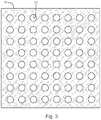
- Fig. 3is a plan view of the aperture array 24 having a plurality of apertures 25.
- the aperture array 24is constructed by patterning a metal mask on the surface of a silicon detector, such as the detector 16 shown in Fig. 2 .
- the lens array 22may be fabricated as etched glass or molded plastic.
- the lens array 22is a custom micro-lens array commercially available from JENOPTIK Optical Systems.
- Fig. 4is a schematic plan view of an optical detection device, according to an embodiment.
- the optical detection device of Fig. 4is configured as a patch 32.
- At least one light source (not shown in Fig. 4 ) and detector 38are arranged in an optical reader, such that the patch 32 , that is configured to be placed on the skin.
- a light sourceis arranged to transmit the excitation light through a central via 34 in the patch 32 , and a single universal detector 38 substantially surrounds the central via 34.
- a plurality of detectorscan be used, for example, substantially encircling the central via 34 to detect the emitted light in a plurality of emission wavelength ranges.
- the optical detection deviceincludes at least one light guiding component 36 in the central via 34.
- the light guiding component 36such as a waveguide or optical fiber, is arranged to guide the excitation light to the skin.
- a plurality of light sourcesare arranged to transmit the excitation light through the central via 34 (e.g., by means of one or more waveguides or optical fibers) in a plurality of different excitation wavelength ranges.
- one or more light sourcesmay be arranged to transmit excitation light to the skin through the central via 34 having a circular cross-section to transmit the excitation light through a substantially circular surface area of the skin having a diameter of about 1 mm and a corresponding excitation surface area of about 0.8 mm 2 .
- the detector 38has a square cross-section and is positioned to detect light emitted from a substantially square surface area of the skin through which the detected light passes as it travels to the detector 38.
- Fig. 5is a schematic exploded view of the patch 32.
- the patch 32includes multiple layers. Dimensions of the patch 32 may be, for example, a diameter of about 16 mm and a thickness T of about 1.6 mm.
- the layersmay include a plastic cover 40 having a thickness of about 200 um, the light control film 26 having a thickness of about 100 um, the filter 28 having a thickness of about 200 um, the lens array 22 having a thickness of about 100 um, and the aperture array 24 patterned on a silicon detector layer 48 having a thickness of about 200 um.
- the layerscan also include a printed circuit board (PCB) 50 having a thickness of about 400 um, a battery 52 having a thickness of about 300 um, and a case 54 having a thickness of about 200 um.
- PCBprinted circuit board
- the PCB 50can include one or more light sources.
- the PCB 50can also include processing electronics and/or a microprocessor in communication with one or more detectors in the detector layer 48 to receive data representative of the light detected in the emission wavelength range and programmed to determine at least one analyte value in dependence upon the data.
- the central via 34may be formed through a stack of the layers (e.g., etched or drilled through the stack in the assembly process).
- Fig. 6is a schematic side view of an optical detection device for monitoring an implant showing an arrangement of detection optics 60 , according to an embodiment.
- light emitted from the implant and tissue in the emission wavelength rangeis transmitted through at least two layers of light control films 62 , 64.
- the two layers of light control films 62 , 64can restrict the light emitted from the tissue from entering the lens array 22 and/or the aperture array 24 based on the incident angle of the emitted light relative to the films 62 , 64.
- the light control film 62comprises alternating transparent and opaque layers in an arrangement which is similar to a Venetian blind. Light propagating from angles greater than a desired incident angle is absorbed.
- the light control film 64may include VikutiTM optical grade micro-louver privacy film commercially available from 3MTM, which blocks light having an incident angle greater than desired (e.g., greater than 24 degrees) relative to a perpendicular line through the film 64.
- the light control film 62 and/or 64may be operable to restrict light emitted from the tissue from entering the lens array 22 and the aperture array 24 based on a combination of incident angle and azimuth.
- the light control film 62 and/or 64may be effective at blocking high angle-of-incidence light having an azimuth substantially perpendicular to the micro-louvers, but may be relatively ineffective at blocking high angle-of-incidence light having an azimuth substantially parallel to the micro-louvers.
- two layers of light control film 62 , 64can be cross-hatched or otherwise disposed such that louvers or other light control elements are non-parallel such that the light control film 62 , 64 are collectively effective at blocking high angle-of-incidence light having different azimuths.
- the films 62 , 64may be substantially the same as each other, or comprises different types of privacy film.
- the filter 28e.g., a dichroic or dielectric filter
- the filter 28may be positioned between the aperture array 24 and the detector 16 to restrict the transmission of the emitted light to the detector 16 to wavelengths substantially within the emission wavelength range(s).
- the operation of the embodiment of Fig. 6can be similar to the operation of the embodiment of Figs. 1-2 previously described.
- Fig. 7is a schematic side view of an optical detection device for monitoring an implant.
- An array of lenses 122is aligned with an array of apertures 24 to restrict the transmission of off-axis light to the detector 16.
- the lens arrays 122 and the aperture array 24are positioned with respect to the detector 16 to restrict the light emitted from the tissue that travels to the detector 16 according to an input angle ⁇ of the emitted light relative to optical axis 30 of the apertures.
- the optical axis 30 of the aperturescan be substantially perpendicular to the surface of the detector 16.
- the lens array 122includes light-blocking elements 72.
- the light-blocking elements 72can be disposed between the apertures 25 to block propagation of off-axis light rays 74 , 76 through the apertures 25.
- the light-blocking elements 72can include black resin, metal, and/or metal film deposited in cavities of a substrate 123 of the lens array 122 positioned.
- At least one filter 28is positioned to restrict the transmission of the emitted light to the detector 16 to wavelengths substantially within the emission wavelength range.
- one or more layers of light control filmmay be included in this embodiment.
- the operation of the embodiment of Fig. 7can be similar to the operation of the embodiment of Figs. 1-2 previously described.
- Figs. 8A-8Ddepict a lens array 122 with light-blocking elements in various stages of fabrication, according to an embodiment.
- Fig. 8Ashows a side view of the lens array 122 which may be fabricated as etched glass or molded plastic.
- the lens array 122is a micro-lens array commercially available from JENOPTIK Optical Systems.
- Fig. 8Bshows cavities 78 which can be, for example, etched or integrally molded into a substrate portion 123 of the lens array 122.
- the cavities 78can be filled with a substantially opaque material to form light-blocking elements 72.
- the light-blocking elements 72can be constructed of, for example, black resin, metal, and/or metal film.
- the aperture array 24may be positioned adjacent to the lens array 122 (with a spacer in some embodiments) such that light-blocking elements 72 are positioned between the apertures 25.
- the aperture array 24is constructed by patterning a metal mask on the surface of a silicon detector and positioning the detector with aperture array 24 adjacent to the lens array 22 with light-blocking elements 72 such that the light-blocking elements 72 are positioned between the between apertures 25.
- Fig. 9is a schematic plan view of an optical detection device 210 , according to an embodiment.
- the optical detection device 210includes four detectors 216 , 220 , 222 , and 224 and a light source 218.
- the optical detection device 210has a relatively large ration of detector surface area to light source surface area (also referred to herein as "surface area ratio").
- the large surface area ratiocan improve detection of implant signals, when the implant is embedded in subcutaneous tissue (e.g., 1-4 mm under the surface of the skin).
- the light source 218 and four detectors 216 , 220 , 222 , 224are arranged such that the ratio of the surface area of the skin through which the detected light passes as it travels to the detectors 216 , 220 , 222 , 224 to the surface area of the skin through which the excitation light is transmitted is at least 4:1.
- the light source 218has a circular cross-section and is positioned to transmit the excitation light through a substantially circular surface area of the skin having a diameter of about 3 mm, a radius of about 1.5 mm, and an excitation surface area of about 7 mm 2 .
- the four detectors 216 , 220 , 222 , 224have square cross-sections and are positioned to detect light emitted from four substantially square surface areas of the skin, through which the detected light passes as it travels to the detectors.
- the optical detection device 210can be configured to detect implant signals at a lateral distance at least twice the depth of the implant.
- at least a portion of at least one of the detectors 216 , 220 , 222 , 224can be at least twice as far away from the implant laterally as that portion is from the implant distally.
- at least a portion of at least one of the detectors 216 , 220 , 222 , 224can be 8 mm away from the center of the light source 218.
- the furthermost edge or corner of at least one of the detectors 216 , 220 , 222 , 224can be at least twice as far away from the center of the light source 218 as the implant is deep.
- the detectorcan have a radius at least twice the depth of the implant.
- the optical detection device 210can be configured to detect implant signals at a lateral distance at least three times, at least five times, or any other suitable multiple of the depth of the implant.
- An optical detector device 210 operable to detect implant signals a relatively large lateral distance from the implantmay be able to detect a larger portion of an emitted signal, particularly in a high-scattering environment. Capturing a larger portion of the emitted signal can improve detection accuracy.
- Fig. 10is a schematic plan view of an optical detection device 310 , according to an embodiment.
- the four detectors 316 , 320 , 322 , 324are positioned closer to the light source 318 as they surround or encircle the light source 318 , and the ratio of detection surface area to excitation surface area is larger.
- the light source 318may have a circular cross-section and is arranged to transmit the excitation light through a substantially circular surface area of the skin having a diameter of about 2 mm, a radius of about 1 mm, and an excitation surface area of about 3.14 mm 2 .
- the four detectors 316 , 320 , 322 , 324have square cross-sections and are positioned to detect light emitted from four substantially square surface areas of the skin, through which the detected light passes as it travels to the detectors.
- Fig. 11is a schematic, plan view of aspects of an optical detection device 410 , according to another embodiment.
- five circular-shaped detectors 428A , 428B , 428C , 428D , and 428Esurround or encircle a central via 434 .
- the central via 434may be a hole in the device 410 .
- a plurality of light sources 426are arranged to transmit excitation light in a plurality of different wavelength ranges through the central via 434 .
- the light sources 426may be arranged to transmit excitation light to the skin through the central via 434 having a circular cross-section to transmit the excitation light through a substantially circular surface area of the skin having a diameter of about 3 mm and a corresponding excitation surface area of about 7 mm 2 .
- the five detectors 428A , 428B , 428C , 428D , and 428Ehave circular cross-sections and are positioned to detect light emitted from five substantially circular surface areas of the skin, through which the detected light passes as it travels to the detectors.
- Embodimentsmay be altered in many ways without departing from the scope of the invention. For example, many different permutations or arrangements of one or more light sources, one or more detectors, filters, and/or light guiding elements connecting the optical components may be used to realize the device and method of the invention. For example, alternative embodiments may have different dimensions and/or wavelengths. Embodiments may include cabled or wireless handheld readers, wireless skin patch readers, bench-top instruments, imaging systems, smartphone attachments and applications, or any other configuration that utilizes the disclosed optics and algorithms.
- a monitoring devicecan be operable to simultaneously emit an excitation optical signal and detect an emission signal.
- the detector of such a monitoring devicecan be shielded from reflected or back-scattering excitation light using apertures, light-blocking elements, filters, light control film, etc.
- a monitoring devicecan be operable to emit an excitation optical signal during one period of time, and detect an emission signal during another period of time in which the excitation optical signal is deactivated.
- Tissue optical heterogeneity in some casesmay be significant.
- a light sourcecan be positioned with a set of moveable filters between the light source and the surface of the skin.
- a single photodetectorcan be utilized in place of separate discrete detector elements.
- the detectormay be used to detect different wavelength ranges by using moveable or changeable filters to enable multiple wavelengths to be measured. Changing or moving filters may be accomplished by a mechanical actuator controlling a rotating disc, filter strip or other means.
- optical filtersmay be coated with a material that, when subjected to current, potential, temperature or another controllable influence, changes optical filtering properties, so that a single photodetector can serve to detect multiple wavelength ranges.
- the devices and methods of the present inventionmake use of wafer-based micro-optics. These systems are created lithographically, but can be replicated at low cost.
- the technologyallows for layers of optics and detectors to be bonded at the wafer level and then diced into individual detector systems. Suitable components include etched refractive lenses, polymer replicated refractive lenses, etched binary lenses, replicated binary lenses, replicated holograms, and replicated volume holograms.
- CMOScomplementary metal-oxide-semiconductor
- CCDcharge charge-coupled device
Landscapes
- Health & Medical Sciences (AREA)
- Physics & Mathematics (AREA)
- Life Sciences & Earth Sciences (AREA)
- Medical Informatics (AREA)
- Surgery (AREA)
- Biophysics (AREA)
- Pathology (AREA)
- Engineering & Computer Science (AREA)
- Biomedical Technology (AREA)
- Heart & Thoracic Surgery (AREA)
- Spectroscopy & Molecular Physics (AREA)
- Molecular Biology (AREA)
- Optics & Photonics (AREA)
- Animal Behavior & Ethology (AREA)
- General Health & Medical Sciences (AREA)
- Public Health (AREA)
- Veterinary Medicine (AREA)
- Investigating, Analyzing Materials By Fluorescence Or Luminescence (AREA)
- Measurement Of The Respiration, Hearing Ability, Form, And Blood Characteristics Of Living Organisms (AREA)
- Investigating Or Analysing Materials By The Use Of Chemical Reactions (AREA)
- Optical Measuring Cells (AREA)
Description
- This application claims priority under 35 U.S.C. § 119(e) to provisional
U.S. patent application no. 61/832,065 U.S. patent application no. 61/832,078 - Some embodiments described herein relate to apparatus and methods for monitoring an implant, and in particular to apparatus and methods for detecting optical signals emitted from an implant with restriction of off-axis light.
- Some embodiments described herein relate to apparatus and methods for monitoring an implant, and in particular to apparatus and methods for detecting optical signals through a relatively large surface area of tissue relative to a surface area of tissue through which an excitation optical signal is supplied.
- The monitoring of the level or concentration of an analyte, such as glucose, lactate, oxygen, etc., in certain individuals is important to their health. High or low levels of glucose, or other analytes, may have detrimental effects or be indicative of specific health states. The monitoring of glucose is particularly important to persons with diabetes, a subset of whom must determine when insulin is needed to reduce glucose levels in their bodies or when additional glucose is needed to raise the level of glucose in their bodies.
- A conventional technique used by many persons with diabetes for monitoring their blood glucose level includes the periodic drawing of blood, the application of that blood to a test strip, and the determination of the blood glucose level using calorimetric, electrochemical, or photometric detection. This technique does not permit continuous or automatic monitoring of glucose levels in the body, but typically must be performed manually on a periodic basis. Unfortunately, the consistency with which the level of glucose is checked varies widely among individuals. Many persons with diabetes find the periodic testing inconvenient, and they sometimes forget to test their glucose level or do not have time for a proper test. In addition, some individuals wish to avoid the pain associated with the test. Unmonitored glucose may result in hyperglycemic or hypoglycemic episodes. An implanted sensor that monitors the individual's analyte levels would enable individuals to monitor their glucose, or other analyte levels, more easily.
- Some known devices perform in situ monitoring of analytes (e.g., glucose) in the blood stream or interstitial fluid of various tissues. A number of these devices use sensors that are inserted into a blood vessel or under the skin of a patient. Communicating and/or retrieving data from such known and/or proposed devices, however, can be challenging. For example, an implanted sensor may be able to communicate with a detector or receiver using radio frequency (RF) transmissions. Such a sensor, however, may require electronics, batteries, antennae, and/or other communication hardware which may increase the bulk of the implanted sensor, may require frequent inconvenient recharging, and/or may decrease the longevity or reliability of the implant.
WO 2013/073270 discloses a measurement device including a light source for emitting measurement light which is used for measuring an in vivo component present in a living body.- A need therefore exists for apparatus and methods for detecting optical signals from an implanted sensor, such that a fluorescent sensor can be used. A fluorescent sensor may not require electric charging and/or transmission electronics. Such implanted sensors, however, may be difficult to read or to monitor optically because of low levels of florescence in the presence of high scatter due to dynamic changes in skin conditions (e.g., blood level and hydration). The skin is highly scattering, and the scattering may dominate the optical propagation. Scatter is caused by index of refraction changes in the tissue, and the main components of scatter in the skin are due to lipids, collagen, and other biological components. The main absorption is caused by blood, melanin, water, and other components.
- Devices and apparatus described herein are suitable for providing accurate and consistent measurement of an analyte by monitoring an implantable sensor in such low-signal, high-scattering environments.
- According to the invention there is provided an apparatus including a light source configured to transmit an excitation optical signal through a first area of skin to an implanted sensor; a plurality of detectors substantially surrounding the light source, the plurality of detectors configured to detect an analyte-dependent optical signal emitted from the implanted sensor through a second surface area of skin in response to the implanted sensor being illuminated by the excitation optical signal, the second surface area of the skin being at least four times the first surface area of the skin; and a lens configured to focus at least a portion of the analyte-dependent optical signal onto the detector. The present invention is defined in the claims. Embodiments not falling under the scope of the claims are mere examples not being part of the present invention.
- Some embodiments described herein relate to an array of lenses. Each lens from the array of lenses can be configured to transmit an analyte-dependent optical signal from an implanted sensor to a detector. A plurality of light-blocking elements can be disposed within a substrate of the array of lenses. Each light blocking element from the array of light-blocking elements can be configured to prevent or inhibit a photon having an angle of incidence greater than a predetermined angle of incidence from passing through the substrate.
- Some embodiments described herein relate to an apparatus including a detector configured to detect an analyte-dependent optical signal from an implanted sensor. A lens can be configured to focus at least a portion of the analyte-dependent optical signal onto the detector. A filter can be configured to attenuate light having wavelengths shorter than the analyte-dependent optical signal.
- Some embodiments described herein relate to an implant capable of emitting, in response to excitation light in at least one excitation wavelength range, at least one analyte-dependent optical signal in at least one emission wavelength range. A device including at least one light source can be arranged to transmit the excitation light through tissue surrounding the implant. The device can include at least one detector arranged to detect light emitted from implanted sensor and transmitted through the tissue in the emission wavelength range. The device can also include an array of lenses arranged with an array of apertures to restrict transmission of off-axis light to the detector. The arrays of lenses and the array of apertures can be positioned with respect to the detector to restrict the light emitted from the tissue that travels to the detector based on the incidence angle of the emitted light. At least one layer of light control film can be arranged with the lens and aperture arrays to restrict the light emitted from the tissue that travels to the detector based on the incidence angle of the emitted light relative to the film. The device can further include at least one filter positioned to restrict transmission of light to the detector to wavelengths substantially within the emission wavelength range.
- Some embodiments described herein relate to an optical detection device is for monitoring an implant embedded in tissue of a mammalian body. The implant is capable of emitting, in response to excitation light in at least one excitation wavelength range, at least one analyte-dependent optical signal in at least one emission wavelength range. The device can include at least one light source arranged to transmit the excitation light through the tissue to the implant. At least one detector is arranged to detect light emitted from the tissue in the emission wavelength range. The device can also include an array of lenses arranged with an array of apertures to restrict transmission of off-axis light to the detector. The arrays of lenses and the array of apertures are positioned with respect to the detector to restrict the light emitted from the tissue that travels to the detector according to an input angle of the emitted light. Light-blocking elements are arranged between the apertures to block propagation of incident light rays through the apertures. The light-blocking elements are positioned to block the incident light rays in accordance with an increase in incident angle of the light rays with respect to optical axes of the apertures. The device further comprises at least one filter arranged to restrict the transmission of the emitted light to the detector to wavelengths substantially within the emission wavelength range.
- Some embodiments described herein relate to a method for monitoring an implant embedded in tissue of a mammalian body. The implant is capable of emitting, in response to excitation light in at least one excitation wavelength range, at least one analyte-dependent optical signal in at least one emission wavelength range. The method can include transmitting the excitation light through the tissue to the implant and detecting light emitted from the tissue in the emission wavelength range. The light in the emission wavelength range is transmitted through an array of lenses and an array of apertures arranged to restrict the light emitted from the tissue that travels to at least one detector according to an input angle of the emitted light. The light in the emission wavelength range is also transmitted through at least one layer of light control film arranged with the lens and aperture arrays to restrict the light emitted from the tissue that travels to the detector according to an incident angle of the emitted light relative to the film. The light in the emission wavelength range is also transmitted through at least one filter positioned to restrict transmission of light to the detector to wavelengths substantially within the emission wavelength range.
- Some embodiments described herein relate to a method for monitoring an implant embedded in tissue of a mammalian body. The implant is capable of emitting, in response to excitation light in at least one excitation wavelength range, at least one analyte-dependent optical signal in at least one emission wavelength range. The method can include transmitting the excitation light through the tissue to the implant and detecting light emitted from the tissue in the emission wavelength range. An array of apertures arranged with an array of lenses restricts the light emitted from the tissue that travels to at least one detector according to an input angle of the emitted light. The method can also include blocking propagation of incident light rays through the apertures using light-blocking elements positioned between the apertures to block the incident light rays having an angle of incidence greater than a threshold angle of incidence based on, for example, the optical axes of the apertures. The method can further include filtering the emitted light to wavelengths substantially within the emission wavelength range.
- Some embodiments described herein relate to an optical detection device for monitoring an implant embedded in tissue under skin. The implant is capable of emitting, in response to excitation light in at least one excitation wavelength range, at least one analyte-dependent optical signal in at least one emission wavelength range. The device can include at least one light source arranged to transmit the excitation light through a first surface area of the skin to the implant embedded in the tissue. One or more detectors can be arranged to detect light that is emitted from at least a second surface area of the skin, wherein the light source and one or more detectors are arranged such that the ratio of the surface area of the skin through which the detected light passes as it travels to the one or more detectors to the surface area of the skin through which the excitation light is transmitted is at least 4:1.
- Some embodiments described herein relate to a method for monitoring an implant embedded in tissue under skin. The implant can be capable of emitting, in response to excitation light in at least one excitation wavelength range, at least one analyte-dependent optical signal in at least one emission wavelength range. The method can include transmitting the excitation light through a first surface area of the skin to the implant embedded in the tissue and detecting light that is emitted from at least a second surface area of the skin. The ratio of the surface area of the skin through which the detected light passes as it travels to one or more detectors to the surface area of the skin through which the excitation light is transmitted is at least 4:1.
Fig. 1 is a schematic side view of an optical detection device for monitoring an implant, according to an embodiment.Fig. 2 is a schematic side view of an optical detection device for monitoring an implant, according to an embodiment.Fig. 3 is a plan view of an aperture array, according to an embodiment.Fig. 4 is a schematic plan view of an optical detection device, according to an embodiment.Fig. 5 is a schematic exploded view of an optical detection device, according to an embodiment.Fig. 6 is a schematic side view of an optical detection device for monitoring an implant, according to an embodiment.Fig. 7 is a schematic side view of an optical detection device for monitoring an implant, according to an embodiment.Figs. 8A-8D depict a lens and aperture array with light-blocking elements in various stages of fabrication, according to an embodiment.Fig. 9 is a schematic plan view of an optical detection device, according to an embodiment.Fig. 10 is a schematic plan view of an optical detection device, according to an embodiment.Fig. 11 is a schematic plan view of an optical detection device, according to an embodiment.- According to some embodiments described herein, an optical detection device is provided for monitoring an implant embedded in tissue of a mammalian body. The implant can include a fluorophore-labeled target capable of emitting, in response to excitation light in at least one excitation wavelength range, at least one analyte-dependent optical signal in at least one emission wavelength range. The optical detection device can be operable to illuminate the implant with light whose wavelength content falls within an absorption band and/or collect light whose wavelength content is in an emission band.
- The optical detection device can include excitation optics including a light source and/or optics operable to generate illumination in the absorption band. The optical detection device can also include emission optics operable to collect fluorescent emissions from the implant. Because in some instances, it may be difficult to obtain, design, and/or implement a light source that has a spectral content (i.e., wavelength range) that exactly matches every fluorophore absorption band, an optical filter or filters (usually band-pass filters) can be used along with the light source to limit the range of illuminating wavelengths to that of the absorption band and/or to reduce illuminating wavelengths of the emission band. Similarly, the emission optics can include another filter or filters operable to allow substantially only light with wavelengths in the emission band to reach the detector and/or to attenuate light with other wavelengths (e.g., light in the absorption band). Similarly stated, the optical detection device can include an optical system design operable to allow substantially only photons with wavelengths in the absorption band reach the target, and substantially only photons with wavelengths in the emission band reach the detector. Without proper optics, photons from the light source may be reach the detector and induce a measurement error.
- Properly designing an optical system for an optical detection device can be complicated in instances in which the amount of emitted fluorescence to be detected is much less than the amount of excitation light scattered (e.g., not absorbed) by an intermediate surface (e.g., skin or tissue disposed between the optical detection device and the implant). One challenge is that the amount of excitation light that reaches the implant may be low because of the absorption and scattering caused by the various body parts (skin, tissue, etc.). The low amount of emitted fluorescence is further reduced by absorption and scattering as it makes its way out of the body towards the detector. Existing optical filter technology, which may provide rejection of unwanted photons on the order of (10-6) may be insufficient in these situations. Another challenge is that the difference between excitation and detection wavelengths (e.g., Stokes shift) may be quite small. A further challenge is that dichroic filters cause shifting (e.g., the "blue shift") of filter wavelengths as a function of the angle of light rays transmitted through the filter. Because of these challenges, standard fluorescence methods would allow through high background levels and, in turn, result in low Signal-to-Background (SBR) and Signal-to-Noise (SNR) ratios.
- Some embodiments described herein relate to a compact device that can accurately and consistently monitor an implanted sensor. Such a device can be worn by a user substantially continuously and/or may not substantially restrict movements or activities of the user. The device and the sensor can collectively allow for continuous and/or automatic monitoring of an analyte and can provide a warning to the person when the level of the analyte is at or near a threshold level. For example, if glucose is the analyte, then the monitoring device might be configured to warn the person of current or impending hyperglycemia or hypoglycemia. The person can then take appropriate actions.
- In the description contained herein, it is understood that all recited connections between structures can be direct operative connections or indirect operative connections through intermediary structures. A set of elements includes one or more elements. Any recitation of an element is understood to refer to at least one element. A plurality of elements includes at least two elements. Unless clearly indicated otherwise, any described method steps need not be necessarily performed in a particular or illustrated order. A first element (e.g. data) derived from a second element encompasses a first element equal to the second element, as well as a first element generated by processing the second element and optionally other data. Making a determination or decision according to a parameter encompasses making the determination or decision according to the parameter and optionally according to other data. Unless otherwise specified, an indicator of some quantity/data may be the quantity/data itself, or an indicator different from the quantity/data itself. Some embodiments described herein reference a wavelength, such as an excitation wavelength or an emission wavelength. Unless clearly indicated otherwise, a wavelength should be understood as describing a band of wavelengths including the wavelength. Computer programs described in some embodiments of the present invention may be stand-alone software entities or sub-entities (e.g., subroutines, code objects) of other computer programs. Computer readable media encompass non-transitory media such as magnetic, optic, and semiconductor storage media (e.g. hard drives, optical disks, flash memory, DRAM), as well as communications links such as conductive cables and fiber optic links. According to some embodiments, the present invention provides, inter alia, computer systems comprising hardware (e.g. one or more processors and associated memory) programmed to perform the methods described herein, as well as computer-readable media encoding instructions to perform the methods described herein.
- The following description illustrates embodiments of the invention by way of example and not necessarily by way of limitation.
Fig.1 is a schematic side view of anoptical detection device 10 for monitoring an implanted sensor orimplant 12, according to an embodiment. Theimplant 12 is embedded intissue 15 of a mammalian body (which may be a piece of tissue that is attached or unattached to the rest of the body in various embodiments). Theimplant 12 can be embedded under a surface ofskin 14. Theimplant 12 can be embedded and/or positioned in the subcutaneous tissue (e.g., in the range of 1 to 4 mm under the surface of the skin14). Theimplant 12 is capable of emitting, in response to excitation light within an excitation wavelength range, at least one analyte-dependent optical signal within an emission wavelength range. The analyte may be, for example, glucose or other analytes in thetissue 15. Suitable optical signals include, without limitation, luminescent, bioluminescent, phosphorescent, autoluminescence, and diffuse reflectance signals. In some embodiments, theimplant 12 contains one or more luminescent dyes (e.g., fluorescent dyes) whose luminescence emission intensity varies in dependence upon the amount or presence of target analyte in the body of the individual (e.g., in tissue15).- A
light source 18 is arranged to transmit excitation light within the excitation wavelength range from the surface of theskin 14, through thetissue 15, and to theimplant 12. Suitable light sources include, without limitation, lasers, semi-conductor lasers, light emitting diodes (LEDs), and organic LEDs.Detectors light source 18 to detect light emitted from the tissue in the emission wavelength range. Suitable detectors include, without limitation, photodiodes, complementary metal-oxide-semiconductor (CMOS) detectors or charge-coupled device (CCD) detectors. Although multiple detectors are shown, a single and/or universal detector can be used. - The detectors can be16,20 filtered (e.g., with dichroic filters or other suitable filters) to measure the optical signals emitted within the wavelength ranges. For example, a suitable luminescent dye sensitive to glucose concentration is Alexa Flour ® 647 responsive to excitation light (absorption) in the range of about 600 to 650 nm (absorption peak 647 nm) and within an emission wavelength range of about 670 to 750 nm with an emission peak of about 680 nm. Thus, in an embodiment in which the sensor includes Alexa Flour ® 647, the
detectors - In some embodiments, the
implant 12 is further capable of emitting, in response to excitation light within a second excitation wavelength range, at least one analyte-independent optical signal within a second emission wavelength range. For example, theimplant 12 can contain an analyte-independent luminescence dye that functions to control for non-analyte physical or chemical effects on a reporter dye (e.g., photo bleaching or pH). Multiple dyes may be used. The analyte-independent optical signal is not modulated by analyte present in thetissue 15 and provides data for normalization, offset corrections, or internal calibration. The analyte-independent signal may compensate for non-analyte affects that are chemical or physiological (e.g., oxygen, pH, redox conditions) or optical (e.g., water, light absorbing/scattering compounds, hemoglobin). Alternatively, the analyte-independent signal may be provided by a stable reference dye in theimplant 12. Suitable stable reference materials include, but are not limited to, lanthanide-doped crystals, lanthanide-doped nanoparticles, quantum dots, chelated lanthanide dyes, and metal (e.g., gold or silver) nanoparticles. The stable reference dye may provide a reference signal for other signals (e.g., to determine photo bleaching). - In the operation of
device 10, thelight source 18 is activated to transmit excitation light within the excitation wavelength range from the surface of theskin 14, through thetissue 15, and to theimplant 12. The dye in theimplant 12 absorbs some of the excitation light and emits fluorescence that depends on glucose or other analyte properties. The light may be emitted from theimplant 12 in all directions, and scattered by thetissue 15. Some of the light that is emitted from theimplant 12 is transmitted through thetissue 15 and detected by at least one of thedetectors skin 14 to theimplant 12. At least one of thedetectors tissue 15 through the surface of theskin 14. - The second optical signal may be used to normalize the primary analyte-dependent optical signal for scattering of light emitted from the
implant 12. At least one corrected signal value may be calculated in dependence upon the measured optical signals. In one example, the primary analyte-dependent signal from the implant may be normalized by the analyte-independent optical signal emitted from theimplant 12. Prior to executing optical reads for the analyte-dependent signal and/or the analyte-independent signal, a dark reading may be taken to account for background or ambient light, and this reading may be used to further correct the signals, e.g., by background subtraction. - In some embodiments, an analyte value (e.g., glucose concentration) is determined from the analyte-dependent signal and/or a ratio of multiple optical signals including one or more reference signals. In one example, the signal from the glucose sensitive fluorophore (e.g., Alexa Flour ® 647) is normalized by the signal from a glucose insensitive fluorophore (e.g., Alexa Flour ® 700). One suitable dye for the analyte-independent signal is Alexa Flour ® 750 which is responsive to excitation light within an excitation wavelength range of about 700 to 760 nm (excitation peak 750 nm) and has an emission wavelength range of about 770 to 850 nm with an emission peak of about 780 nm.
- An analyte value can be determined based on the optical signal(s) using, for example, a look-up table or calibration curve. Determining the analyte value can be implemented in software (executing on a processor) and/or hardware. For example, the
optical device 10 can include a microprocessor. In some embodiments, the microprocessor is programmed to store measured optical signal values in a memory and/or to calculate normalized signal values and analyte concentrations. Alternatively, these functions may be performed in a separate processor or external computer in communication with theoptical device 10. The external processor or computer can receive data representative of the measured optical signals and calculates the corrected signal value and analyte concentration. Alternatively, multiple processors may be provided, e.g., providing one or more processors in the optical device that communicate (wirelessly or with wires) with one or more external processors or computers. - In some embodiments in which two implant dyes (e.g., luminescent dyes) are utilized, it is possible that the implant dyes may share or overlap excitation (absorption) or emission wavelength ranges. In one example, the emission wavelength range of the first dye, which provides the analyte-dependent luminescence signal, shares or overlaps the excitation wavelength range of the second dye, which provides the analyte-independent luminescence signal. In another embodiment, the first and second dyes may share or overlap excitation wavelength ranges (so that a common light source may be used) and emit optical signals within different emission wavelength ranges. In another embodiment, the first and second dyes may be excited by light within different excitation wavelength ranges and emit optical signals within the same or overlapping emission wavelength range(s).
- The
implant 12 can be embedded in subcutaneous tissue (e.g., 1 to 4 mm under the surface of the skin14). In some embodiments, theimplant 12 comprises hydrogel scaffolds embedded with glucose-sensing nanospheres. The design of theimplant 12 can use injectable, tissue-integrating, vascularizing scaffolds as the sensor. Embedded nanospheres emit luminescence that changes intensity and lifetime in response to the presence or concentration of the analyte (e.g., interstitial glucose). The spacing distances between each of thedetectors light source 18 determine the depths of the respective light paths for detecting optical signals from theimplant 12. The combination of an excitation light source and a detection band is an optical channel. Thelight source 18 anddetectors skin 14 through which the excitation light is transmitted is located between substantially surrounding surface areas ofskin 14 through which the detected light passes as it travels from thetissue 15 to one ormore detectors - Although only one
light source 18 and twodetectors Fig.1 , in some embodiments, theoptical device 10 can have any number of light sources and any number of detectors. Theoptical device 10 can have multiple possible combinations of spacing distances between multiple light sources and detectors. Such a multiple light source and/or multiple detector implementation can allow increased flexibility of theoptical device 10. For example, since the depth of theimplant 12 may be application-specific, anoptical device 10 having multiple light sources and/or multiple detectors can be used for multiple applications. - The
optical device 10 can be configured to ensure that substantially only photons with wavelengths in the excitation wavelength range(s) reach theimplant 12, and substantially only photons with wavelengths in the emission wavelength ranges(s) reach at least one of thedetectors light source 18 reaching thedetectors Fig.2 is a schematic side view of an optical detection device for monitoring an implant, according to an embodiment. An array oflenses 22 is aligned with an array ofapertures 24 to restrict transmission of off-axis light to thedetector 16. Thelens arrays 22 and theaperture array 24 are positioned with respect to thedetector 16 to collectively restrict the light emitted from the tissue that travels to thedetector 16 based on an input angleθ (also referred to herein as incident angle) of the emitted light relative tooptical axes 30 of the apertures. Theoptical axes 30 of the apertures can be substantially perpendicular to the surface of thedetector 16. Each aperture from the array ofapertures 24 can be substantially aligned with a lens from the array oflenses 22. Similarly stated theoptical axes 30 of the apertures can be substantially coaxial with the center and/or axes of the lenses. For example, a substantially opaque portion of the array ofapertures 24 can be positioned below the edges of the lenses.- At least one layer of
light control film 26 is arranged with thelens array 22 and theaperture array 24. Thelight control film 26 can restrict the light emitted from the tissue from entering thelens array 22 and/or theaperture array 24 based on the incident angle of the emitted light relative to thefilm 26. In one example, thelight control film 26 is Vikuti™ optical grade micro-louver privacy film commercially available from 3M™, which can block light having an incident angle greater than desired (e.g., greater than 24 degrees) relative to a perpendicular line through thefilm 26. This privacy film comprises a set of microlouvers that prevent light from large incident angles from reaching thelens array 22. In other embodiments, thefilm 26 comprises alternating transparent and opaque layers in an arrangement which is similar to a Venetian blind. Light propagating from angles greater than a desired incident angle can be absorbed and/or reflected. - At least one filter28 (e.g., a dichroic or dielectric filter) is positioned to restrict transmission of light to the
detector 16 to wavelengths substantially within the desired emission wavelength range. Because the detection of optical signals is dominated by low levels of return signals relative to the excitation light, thefilter 28 can prevent scattered excitation light from blinding thedetector 16. Suitable filters include band-pass, low-pass, and high pass filters depending upon the desired emission wavelength range for an application. Some modern optical filters have demonstrated 10-9 light rejection due to improvements in coating technologies. Additionally, intermediate layers of the optical detection system (e.g., thelens array 22, theaperture array 24, etc.) can include anti-reflective coatings to reduce or prevent light leaking through to thedetector 16. - Due to fundamental properties of dichroic filters, maintaining a high level of light rejection requires careful design. One property of dichroic filters that detracts from light rejection is the "blue shift" as a function of input angle, where the transmittance wavelengths of dichroic filters change as a function of input angle. For the detection light emitted from the implant, there is a trade off between the input angle and the absolute optical signal. The light leaving the tissue is highly scattered and may form a lambertian distribution by the time it reaches the surface of the skin. The collection efficiency of the emitted light is proportional to ∼NA2, where NA=Numerical Aperture = n sinθ, andθ is the input angle. To improve the collection efficiency, the allowable input angle θ can be increased without increasing the angle so much to allow excitation light though the
filter 28. - The
lens array 22 and theaperture array 24 control the input angleθ of light traveling to thedetector 16. Thelens array 22 and anaperture array 24 restrict the light to an input angle less thanθ, which in some embodiments is selected to be +/- 20 degrees. The input angleθ can be controlled by varying the size of the apertures and the focal length of the micro lenses in thelens array 22. The smaller the aperture, then the smaller is input angleθ. The longer the focal length, then the smaller is input angleθ. Although not shown, a spacer can be used to maintain separation between the surface of theaperture array 24 and thelens array 22. Fig.3 is a plan view of theaperture array 24 having a plurality ofapertures 25. In some embodiments, theaperture array 24 is constructed by patterning a metal mask on the surface of a silicon detector, such as thedetector 16 shown inFig.2 . Thelens array 22 may be fabricated as etched glass or molded plastic. In some embodiments, thelens array 22 is a custom micro-lens array commercially available from JENOPTIK Optical Systems.Fig.4 is a schematic plan view of an optical detection device, according to an embodiment. The optical detection device ofFig.4 is configured as apatch 32. At least one light source (not shown inFig.4 ) anddetector 38 are arranged in an optical reader, such that thepatch 32, that is configured to be placed on the skin. A light source is arranged to transmit the excitation light through a central via34 in thepatch 32, and a singleuniversal detector 38 substantially surrounds the central via34. In other embodiments, instead of thesingle detector 38, a plurality of detectors can be used, for example, substantially encircling the central via34 to detect the emitted light in a plurality of emission wavelength ranges. In some embodiments, the optical detection device includes at least onelight guiding component 36 in the central via34. Thelight guiding component 36, such as a waveguide or optical fiber, is arranged to guide the excitation light to the skin. In some embodiments, a plurality of light sources (not shown for clarity inFig.4 ) are arranged to transmit the excitation light through the central via34 (e.g., by means of one or more waveguides or optical fibers) in a plurality of different excitation wavelength ranges.- As one possible example, one or more light sources may be arranged to transmit excitation light to the skin through the central via34 having a circular cross-section to transmit the excitation light through a substantially circular surface area of the skin having a diameter of about 1 mm and a corresponding excitation surface area of about 0.8 mm2. The
detector 38 has a square cross-section and is positioned to detect light emitted from a substantially square surface area of the skin through which the detected light passes as it travels to thedetector 38. The detection surface area is substantially square with sides of 10 mm length, so that the total detection surface area is (10 mm x 10 mm) - 1 mm2 = 99 mm2. Accordingly, in this example, the ratio of detection surface area to excitation surface area is greater than 120:1. Fig.5 is a schematic exploded view of thepatch 32. Thepatch 32 includes multiple layers. Dimensions of thepatch 32 may be, for example, a diameter of about 16 mm and a thickness T of about 1.6 mm. In some embodiments, the layers may include aplastic cover 40 having a thickness of about 200 um, thelight control film 26 having a thickness of about 100 um, thefilter 28 having a thickness of about 200 um, thelens array 22 having a thickness of about 100 um, and theaperture array 24 patterned on asilicon detector layer 48 having a thickness of about 200 um. The layers can also include a printed circuit board (PCB)50 having a thickness of about 400 um, abattery 52 having a thickness of about 300 um, and acase 54 having a thickness of about 200 um. ThePCB 50 can include one or more light sources. ThePCB 50 can also include processing electronics and/or a microprocessor in communication with one or more detectors in thedetector layer 48 to receive data representative of the light detected in the emission wavelength range and programmed to determine at least one analyte value in dependence upon the data. The central via34 may be formed through a stack of the layers (e.g., etched or drilled through the stack in the assembly process).Fig.6 is a schematic side view of an optical detection device for monitoring an implant showing an arrangement ofdetection optics 60, according to an embodiment. In this embodiment, light emitted from the implant and tissue in the emission wavelength range is transmitted through at least two layers oflight control films light control films lens array 22 and/or theaperture array 24 based on the incident angle of the emitted light relative to thefilms light control film 62 comprises alternating transparent and opaque layers in an arrangement which is similar to a Venetian blind. Light propagating from angles greater than a desired incident angle is absorbed. Thelight control film 64 may include Vikuti™ optical grade micro-louver privacy film commercially available from 3M™, which blocks light having an incident angle greater than desired (e.g., greater than 24 degrees) relative to a perpendicular line through thefilm 64.- In some embodiments, the
light control film 62 and/or64 may be operable to restrict light emitted from the tissue from entering thelens array 22 and theaperture array 24 based on a combination of incident angle and azimuth. For example, in an embodiment where thelight control film 62 and/or64 includes multiple micro-louvers, thelight control film 62 and/or64 may be effective at blocking high angle-of-incidence light having an azimuth substantially perpendicular to the micro-louvers, but may be relatively ineffective at blocking high angle-of-incidence light having an azimuth substantially parallel to the micro-louvers. In some such embodiments, two layers oflight control film light control film - In some embodiments, the
films aperture array 24 and thedetector 16 to restrict the transmission of the emitted light to thedetector 16 to wavelengths substantially within the emission wavelength range(s). The operation of the embodiment ofFig.6 can be similar to the operation of the embodiment ofFigs.1-2 previously described. Fig.7 is a schematic side view of an optical detection device for monitoring an implant. An array oflenses 122 is aligned with an array ofapertures 24 to restrict the transmission of off-axis light to thedetector 16. Thelens arrays 122 and theaperture array 24 are positioned with respect to thedetector 16 to restrict the light emitted from the tissue that travels to thedetector 16 according to an input angleθ of the emitted light relative tooptical axis 30 of the apertures. Theoptical axis 30 of the apertures can be substantially perpendicular to the surface of thedetector 16.- The
lens array 122 includes light-blockingelements 72. The light-blockingelements 72 can be disposed between theapertures 25 to block propagation of off-axis light rays74,76 through theapertures 25. The light-blockingelements 72 can include black resin, metal, and/or metal film deposited in cavities of asubstrate 123 of thelens array 122 positioned. At least onefilter 28 is positioned to restrict the transmission of the emitted light to thedetector 16 to wavelengths substantially within the emission wavelength range. Optionally, one or more layers of light control film may be included in this embodiment. The operation of the embodiment ofFig.7 can be similar to the operation of the embodiment ofFigs.1-2 previously described. Figs.8A-8D depict alens array 122 with light-blocking elements in various stages of fabrication, according to an embodiment.Fig.8A shows a side view of thelens array 122 which may be fabricated as etched glass or molded plastic. In some embodiments, thelens array 122 is a micro-lens array commercially available from JENOPTIK Optical Systems.Fig.8B showscavities 78 which can be, for example, etched or integrally molded into asubstrate portion 123 of thelens array 122. As shown inFig.8C , thecavities 78 can be filled with a substantially opaque material to form light-blockingelements 72. The light-blockingelements 72 can be constructed of, for example, black resin, metal, and/or metal film. As shown inFig.8D , theaperture array 24 may be positioned adjacent to the lens array122 (with a spacer in some embodiments) such that light-blockingelements 72 are positioned between theapertures 25. In some embodiments, theaperture array 24 is constructed by patterning a metal mask on the surface of a silicon detector and positioning the detector withaperture array 24 adjacent to thelens array 22 with light-blockingelements 72 such that the light-blockingelements 72 are positioned between the betweenapertures 25.Fig.9 is a schematic plan view of anoptical detection device 210, according to an embodiment. Theoptical detection device 210 includes fourdetectors light source 218. Theoptical detection device 210 has a relatively large ration of detector surface area to light source surface area (also referred to herein as "surface area ratio"). The large surface area ratio can improve detection of implant signals, when the implant is embedded in subcutaneous tissue (e.g., 1-4 mm under the surface of the skin). In particular, thelight source 218 and fourdetectors detectors light source 218 has a circular cross-section and is positioned to transmit the excitation light through a substantially circular surface area of the skin having a diameter of about 3 mm, a radius of about 1.5 mm, and an excitation surface area of about 7 mm2. The fourdetectors - In some embodiments, the
optical detection device 210 can be configured to detect implant signals at a lateral distance at least twice the depth of the implant. For example, at least a portion of at least one of thedetectors light source 218 is centered over an implant that is embedded under 4 mm of tissue, at least a portion of at least one of thedetectors light source 218. Similarly stated, the furthermost edge or corner of at least one of thedetectors light source 218 as the implant is deep. In an alternate embodiment, such as an embodiment having a single or universal detector, the detector can have a radius at least twice the depth of the implant. In other embodiments, theoptical detection device 210 can be configured to detect implant signals at a lateral distance at least three times, at least five times, or any other suitable multiple of the depth of the implant. Anoptical detector device 210 operable to detect implant signals a relatively large lateral distance from the implant may be able to detect a larger portion of an emitted signal, particularly in a high-scattering environment. Capturing a larger portion of the emitted signal can improve detection accuracy. Fig.10 is a schematic plan view of anoptical detection device 310, according to an embodiment. As compared to theoptical detection device 210, in this embodiment, the fourdetectors light source 318 as they surround or encircle thelight source 318, and the ratio of detection surface area to excitation surface area is larger. For example, thelight source 318 may have a circular cross-section and is arranged to transmit the excitation light through a substantially circular surface area of the skin having a diameter of about 2 mm, a radius of about 1 mm, and an excitation surface area of about 3.14 mm2. The fourdetectors Fig.11 is a schematic, plan view of aspects of anoptical detection device 410, according to another embodiment. In this embodiment, five circular-shaped detectors428A,428B,428C,428D, and428E surround or encircle a central via434. The central via434 may be a hole in thedevice 410. A plurality oflight sources 426 are arranged to transmit excitation light in a plurality of different wavelength ranges through the central via434. As one possible example, thelight sources 426 may be arranged to transmit excitation light to the skin through the central via434 having a circular cross-section to transmit the excitation light through a substantially circular surface area of the skin having a diameter of about 3 mm and a corresponding excitation surface area of about 7 mm2. The five detectors428A,428B,428C,428D, and428E have circular cross-sections and are positioned to detect light emitted from five substantially circular surface areas of the skin, through which the detected light passes as it travels to the detectors. Each of the five detection surface areas is substantially circular with a diameter of 5 mm, so that the total detection surface area is 5 x 19.6 mm2 = 98 mm2. Accordingly, in this example, the ratio of detection surface area to excitation surface area is slightly greater than 13:1.- It will be clear to one skilled in the art that the above embodiments may be altered in many ways without departing from the scope of the invention. For example, many different permutations or arrangements of one or more light sources, one or more detectors, filters, and/or light guiding elements connecting the optical components may be used to realize the device and method of the invention. For example, alternative embodiments may have different dimensions and/or wavelengths. Embodiments may include cabled or wireless handheld readers, wireless skin patch readers, bench-top instruments, imaging systems, smartphone attachments and applications, or any other configuration that utilizes the disclosed optics and algorithms.
- In some embodiments described herein, a monitoring device can be operable to simultaneously emit an excitation optical signal and detect an emission signal. For example, the detector of such a monitoring device can be shielded from reflected or back-scattering excitation light using apertures, light-blocking elements, filters, light control film, etc. In other embodiments, a monitoring device can be operable to emit an excitation optical signal during one period of time, and detect an emission signal during another period of time in which the excitation optical signal is deactivated.
- Tissue optical heterogeneity in some cases may be significant. Thus, it may be advantageous to utilize a single light source and a single detector to assure that every color passes through the same optical pathway through the tissue. In one embodiment, a light source can be positioned with a set of moveable filters between the light source and the surface of the skin. Similarly a single photodetector can be utilized in place of separate discrete detector elements. The detector may be used to detect different wavelength ranges by using moveable or changeable filters to enable multiple wavelengths to be measured. Changing or moving filters may be accomplished by a mechanical actuator controlling a rotating disc, filter strip or other means. Alternatively, optical filters may be coated with a material that, when subjected to current, potential, temperature or another controllable influence, changes optical filtering properties, so that a single photodetector can serve to detect multiple wavelength ranges.
- In some embodiments, the devices and methods of the present invention make use of wafer-based micro-optics. These systems are created lithographically, but can be replicated at low cost. The technology allows for layers of optics and detectors to be bonded at the wafer level and then diced into individual detector systems. Suitable components include etched refractive lenses, polymer replicated refractive lenses, etched binary lenses, replicated binary lenses, replicated holograms, and replicated volume holograms.
- In some embodiments, a complementary metal-oxide-semiconductor (CMOS) detector may be used as an integral part of the optical system. The advantage of a CMOS sensor is the ability to integrate the detection, excitation, and digital filtering circuitry into a single piece of silicon. A new technology was recently announced, sCMOS, where researchers have been able to greatly reduce the noise in CMOS detectors to be comparable to charge charge-coupled device (CCD) detectors. Another benefit to a CMOS integrated solution is the ability to perform lock-in detection and digital filtering on the signals to reduce or eliminate the impact of ambient light.
- While various embodiments have been described above, it should be understood that they have been presented by way of example only, not limitation, and various changes in form and details may be made. Any portion of the apparatus and/or methods described herein may be combined in any combination, except mutually exclusive combinations. The embodiments described herein can include various combinations and/or sub-combinations of the functions, components and/or features of the different embodiments described.
Claims (12)
- An apparatus, comprising:a light source (18) configured to transmit an excitation optical signal through a first area of skin (14) to an implanted sensor (12);a plurality of detectors (16, 20) substantially surrounding the light source (18), the plurality of detectors (16, 20) configured to detect an analyte-dependent optical signal emitted from the implanted sensor (12) through a second surface area of skin (14) in response to the implanted sensor (12) being illuminated by the excitation optical signal, the second surface area of the skin (14) being at least four times the first surface area of the skin (14); anda lens (22) configured to focus at least a portion of the analyte-dependent optical signal onto the detectors (16, 20).
- The apparatus of claim 1, further comprising:
an aperture (24) configured to inhibit a photon having an angle of incidence greater than a predetermined angle of incidence from striking the detector (16, 20). - The apparatus of claim 1, wherein the lens (22) is a first lens from an array of lenses (22) defining a first lens axis, the apparatus further comprising:
a second lens (22) from the array of lenses (22) defining a second lens axis substantially parallel to and non-coaxial with the first lens axis. - The apparatus of claim 1, wherein the lens is a first lens from an array of lenses, the apparatus further comprising:
an array of apertures (24), each aperture from the array of apertures (24) being substantially aligned with a center of a lens from the array of lenses (22). - The apparatus of claim 1, further comprising:
a filter (28) configured to attenuate optical signals having wavelengths associated with the light source (18), the filter (28) configured to transmit the analyte-dependent optical signal with substantially no attenuation. - The apparatus of claim 1, further comprising:
a dichroic filter (28) configured to attenuate optical signals having wavelengths associated with the light source (18), the dichroic filter (18) configured to blue shift analyte-dependent optical signals towards the wavelength associated with the light source (18) as a function of an angle of incidence, the detector (16, 20) not being configured to detect a blue-shifted analyte-dependent optical signal. - The apparatus of claim 6, wherein a portion of the excitation optical signal is scattered by tissue surrounding the implanted sensor (12), the apparatus further comprising:
an aperture (24), (1) the lens (22), (2) the aperture (24), and (3) the dichroic filter (28) are collectively configured to inhibit the portion of the excitation optical signal from entering the detector (16, 20). - The apparatus of claim 1, wherein the detector (16, 20) defines a via (34), the light source (18) configured to transmit the excitation optical signal to the implanted sensor (12) through the via (34).
- The apparatus of claim 1, wherein the detector (16, 20) is one of a plurality of detectors (16, 20), the apparatus further comprising:
a base defining a via (34), the light source (18) configured to transmit the excitation optical signal to the implanted sensor (12) through the via (34), the plurality of detectors (16, 20) coupled to the base and substantially surrounding the via (34). - The apparatus of claim 1, wherein:the light source (18) is configured to transmit the excitation signal to the implanted sensor (12) at a depth of at least 1 mm under a surface of a skin (14); andat least a portion of a detector (16, 20) from the plurality of detectors is spaced at least 2 mm from the light source (18) such that at least the portion of the detector (16, 20) is spaced apart from the via (34) at least twice the depth of the sensor (12).
- The apparatus of claim 1, wherein a ratio of the second surface area to the first surface area is greater than 13:1.
- A system including the apparatus of any preceding claim, the system further comprising:the implanted sensor (12) adapted to be disposed a depth beneath the skin (14), andat least a portion of the detector (16, 20) is adapted to be spaced a lateral distance from the implant, the lateral distance being at least twice the depth.
Priority Applications (1)
| Application Number | Priority Date | Filing Date | Title |
|---|---|---|---|
| EP20176588.0AEP3777656A1 (en) | 2013-06-06 | 2014-06-06 | Apparatus for detecting optical signals from implanted sensors |
Applications Claiming Priority (3)
| Application Number | Priority Date | Filing Date | Title |
|---|---|---|---|
| US201361832065P | 2013-06-06 | 2013-06-06 | |
| US201361832078P | 2013-06-06 | 2013-06-06 | |
| PCT/US2014/041284WO2014197786A2 (en) | 2013-06-06 | 2014-06-06 | Apparatus and methods for detecting optical signals from implanted sensors |
Related Child Applications (1)
| Application Number | Title | Priority Date | Filing Date |
|---|---|---|---|
| EP20176588.0ADivisionEP3777656A1 (en) | 2013-06-06 | 2014-06-06 | Apparatus for detecting optical signals from implanted sensors |
Publications (3)
| Publication Number | Publication Date |
|---|---|
| EP3003131A2 EP3003131A2 (en) | 2016-04-13 |
| EP3003131A4 EP3003131A4 (en) | 2017-01-18 |
| EP3003131B1true EP3003131B1 (en) | 2020-05-27 |
Family
ID=52006018
Family Applications (2)
| Application Number | Title | Priority Date | Filing Date |
|---|---|---|---|
| EP14807637.5AActiveEP3003131B1 (en) | 2013-06-06 | 2014-06-06 | Apparatus for detecting optical signals from implanted sensors |
| EP20176588.0AWithdrawnEP3777656A1 (en) | 2013-06-06 | 2014-06-06 | Apparatus for detecting optical signals from implanted sensors |
Family Applications After (1)
| Application Number | Title | Priority Date | Filing Date |
|---|---|---|---|
| EP20176588.0AWithdrawnEP3777656A1 (en) | 2013-06-06 | 2014-06-06 | Apparatus for detecting optical signals from implanted sensors |
Country Status (8)
| Country | Link |
|---|---|
| US (3) | US10219729B2 (en) |
| EP (2) | EP3003131B1 (en) |
| JP (3) | JP2016523608A (en) |
| CN (2) | CN105307559B (en) |
| AU (1) | AU2014274784B2 (en) |
| BR (1) | BR112015029988A2 (en) |
| CA (1) | CA2913474C (en) |
| WO (1) | WO2014197786A2 (en) |
Families Citing this family (51)
| Publication number | Priority date | Publication date | Assignee | Title |
|---|---|---|---|---|
| EP3175780A1 (en) | 2003-12-18 | 2017-06-07 | Metronom Health, Inc. | Implantable biosensor and methods of use thereof |
| US9517023B2 (en) | 2009-06-01 | 2016-12-13 | Profusa, Inc. | Method and system for directing a localized biological response to an implant |
| US10010272B2 (en) | 2010-05-27 | 2018-07-03 | Profusa, Inc. | Tissue-integrating electronic apparatus |
| CA3012355C (en) | 2010-10-06 | 2023-05-16 | Profusa, Inc. | Tissue-integrating sensors |
| US10292784B2 (en)* | 2010-12-10 | 2019-05-21 | Illumix Surgical Canada Inc. | Illuminating surgical device |
| US8945209B2 (en) | 2011-05-20 | 2015-02-03 | Edwards Lifesciences Corporation | Encapsulated heart valve |
| US9693862B2 (en) | 2012-07-31 | 2017-07-04 | Edwards Lifesciences Corporation | Holders for prosthetic heart valves |
| EP2970318B1 (en) | 2013-03-14 | 2018-11-21 | Profusa, Inc. | Oxygen sensors comprising a polymer and a luminescent dye |
| CN113274007B (en) | 2013-03-14 | 2024-10-18 | 普罗菲尤萨股份有限公司 | Method and device for correcting an optical signal |
| EP3003131B1 (en) | 2013-06-06 | 2020-05-27 | Profusa, Inc. | Apparatus for detecting optical signals from implanted sensors |
| JP6539876B2 (en) | 2014-03-31 | 2019-07-10 | ソニー株式会社 | Measuring device, measuring method, program and recording medium |
| US10542920B2 (en)* | 2014-03-31 | 2020-01-28 | Sony Corporation | Measurement device, measurement method, program, and recording medium |
| US10092197B2 (en) | 2014-08-27 | 2018-10-09 | Apple Inc. | Reflective surfaces for PPG signal detection |
| US10215698B2 (en) | 2014-09-02 | 2019-02-26 | Apple Inc. | Multiple light paths architecture and obscuration methods for signal and perfusion index optimization |
| JP2016205954A (en)* | 2015-04-21 | 2016-12-08 | ルネサスエレクトロニクス株式会社 | Magnetic measuring device |
| WO2016210415A1 (en)* | 2015-06-25 | 2016-12-29 | Colvin Arthur E Jr | Transcutaneous reader for use with implantable analyte sensors |
| AU2016315838B2 (en) | 2015-09-02 | 2022-07-28 | Metronom Health, Inc. | Systems and methods for continuous health monitoring using an opto-enzymatic analyte sensor |
| US10080653B2 (en) | 2015-09-10 | 2018-09-25 | Edwards Lifesciences Corporation | Limited expansion heart valve |
| US10687717B1 (en)* | 2015-09-30 | 2020-06-23 | Apple Inc. | PPG sensor having light arrival angle control at detector |
| US10667904B2 (en) | 2016-03-08 | 2020-06-02 | Edwards Lifesciences Corporation | Valve implant with integrated sensor and transmitter |
| US10082387B2 (en)* | 2016-03-09 | 2018-09-25 | UbiQD, Inc. | Fluorescent liquid penetrants and methods of nondestructive testing |
| JP2017213040A (en)* | 2016-05-30 | 2017-12-07 | セイコーエプソン株式会社 | Biological information acquisition apparatus and biological information acquisition method |
| EP3558118A4 (en) | 2016-12-21 | 2021-02-24 | Profusa, Inc. | Polymerizable near-ir dyes |
| WO2018119400A1 (en) | 2016-12-22 | 2018-06-28 | Profusa, Inc. | System and single-channel luminescent sensor for and method of determining analyte value |
| US10918322B2 (en) | 2017-02-13 | 2021-02-16 | Apple Inc. | Light restriction designs in optical sensing applications having shared windows |
| US10463485B2 (en) | 2017-04-06 | 2019-11-05 | Edwards Lifesciences Corporation | Prosthetic valve holders with automatic deploying mechanisms |
| US10792378B2 (en) | 2017-04-28 | 2020-10-06 | Medtronics Minimed, Inc. | Using a blue-shifted reference dye in an optical glucose assay |
| EP3614969B1 (en) | 2017-04-28 | 2023-05-03 | Edwards Lifesciences Corporation | Prosthetic heart valve with collapsible holder |
| DE102017110216B4 (en)* | 2017-05-11 | 2023-03-09 | OSRAM Opto Semiconductors Gesellschaft mit beschränkter Haftung | Optoelectronic sensor module and method for producing an optoelectronic sensor module |
| WO2018237020A1 (en) | 2017-06-21 | 2018-12-27 | Edwards Lifesciences Corporation | CARDIAC EXPANDED CARDIAC VALVES IN THE FORM OF DOUBLE THREAD |
| BR112019027709A2 (en) | 2017-06-29 | 2020-08-11 | Profusa, Inc. | integration sensors in multi-analyte detection fabrics |
| CN114947741B (en) | 2017-09-26 | 2025-08-08 | 苹果公司 | Concentric structures for optical sensing |
| EP3694562A2 (en) | 2017-10-13 | 2020-08-19 | Edwards Lifesciences Corporation | Method for sterilizing heart valves |
| EP3473172A1 (en)* | 2017-10-20 | 2019-04-24 | Universität Zürich | Apparatus for measuring optical parameters in scattering media |
| CN107677604A (en)* | 2017-10-31 | 2018-02-09 | 广东省测试分析研究所(中国广州分析测试中心) | A kind of miniaturization detection means of Visual retrieval card |
| CN109717876B (en)* | 2017-10-31 | 2023-12-26 | 心脏起搏器股份公司 | Structural diffusion membrane for chemical sensors |
| EP3729059B1 (en)* | 2017-12-19 | 2023-05-03 | The Research Foundation for the State University of New York | System for detecting biomarkers comprising an implantable spr sensor |
| JP2021508548A (en)* | 2017-12-28 | 2021-03-11 | プロフサ,インコーポレイテッド | Systems and methods for analyzing biochemical sensor data |
| KR102620446B1 (en)* | 2018-06-22 | 2024-01-03 | 삼성전자주식회사 | Sensor including first optical member having reflection characteristics and second optical member having absorption characteristics absorbable reflected light by first optical member and electronic device with the same |
| CA3104346A1 (en) | 2018-06-27 | 2020-01-02 | Profusa, Inc. | Near-ir glucose sensors |
| WO2020163145A1 (en) | 2019-02-05 | 2020-08-13 | Edwards Lifesciences Corporation | Prosthetic heart valve with suture loop preventing member |
| US11864906B2 (en) | 2019-06-20 | 2024-01-09 | International Business Machines Corporation | LIDAR implantable biosensor for imaging biological tissue |
| WO2021025979A1 (en) | 2019-08-02 | 2021-02-11 | Edwards Lifesciences Corporation | Rotary application of fibrous material to medical devices |
| WO2021035047A1 (en) | 2019-08-20 | 2021-02-25 | Profusa, Inc. | Optical filter device, system, and method for improved optical rejection of out-of-band wavelengths |
| KR20220106815A (en)* | 2019-12-06 | 2022-07-29 | 브로리스 센서 테크놀로지, 유에이비 | Systems and methods for measuring the concentration of an analyte |
| CR20210655A (en) | 2019-12-16 | 2022-06-02 | Edwards Lifesciences Corp | Valve holder assembly with suture looping protection |
| US11561345B2 (en)* | 2020-02-14 | 2023-01-24 | Google Llc | Apertures for reduced dynamic crosstalk and stray light control |
| US12204125B2 (en) | 2020-02-19 | 2025-01-21 | Profusa, Inc. | Optical filter device, system, and methods for improved optical rejection of high angle of incidence (AOI) light |
| US12317024B2 (en)* | 2021-01-14 | 2025-05-27 | Apple Inc. | Electronic devices with skin sensors |
| EP4288764B1 (en)* | 2021-02-03 | 2025-07-09 | Siemens Healthcare Diagnostics, Inc. | High-sensitivity chemiluminescence detection systems and methods |
| EP4575467A1 (en)* | 2023-12-22 | 2025-06-25 | F. Hoffmann-La Roche AG | Techniques for illumination and detection in analytical analyzers |
Family Cites Families (228)
| Publication number | Priority date | Publication date | Assignee | Title |
|---|---|---|---|---|
| JPS59189828A (en) | 1983-04-08 | 1984-10-27 | 萩原 文二 | Subcateneous measuring sensor and apparatus of blood coloring matter |
| US4703756A (en) | 1986-05-06 | 1987-11-03 | The Regents Of The University Of California | Complete glucose monitoring system with an implantable, telemetered sensor module |
| US4975581A (en)* | 1989-06-21 | 1990-12-04 | University Of New Mexico | Method of and apparatus for determining the similarity of a biological analyte from a model constructed from known biological fluids |
| US6040194A (en) | 1989-12-14 | 2000-03-21 | Sensor Technologies, Inc. | Methods and device for detecting and quantifying substances in body fluids |
| US5342789A (en) | 1989-12-14 | 1994-08-30 | Sensor Technologies, Inc. | Method and device for detecting and quantifying glucose in body fluids |
| US5094958A (en) | 1990-08-30 | 1992-03-10 | Fiberchem Inc. | Method of self-compensating a fiber optic chemical sensor |
| US5284140A (en) | 1992-02-11 | 1994-02-08 | Eli Lilly And Company | Acrylic copolymer membranes for biosensors |
| IL107396A (en)* | 1992-11-09 | 1997-02-18 | Boehringer Mannheim Gmbh | Method and apparatus for analytical determination of glucose in a biological matrix |
| US5462880A (en) | 1993-09-13 | 1995-10-31 | Optical Sensors Incorporated | Ratiometric fluorescence method to measure oxygen |
| US5882494A (en) | 1995-03-27 | 1999-03-16 | Minimed, Inc. | Polyurethane/polyurea compositions containing silicone for biosensor membranes |
| JPH08304741A (en)* | 1995-05-09 | 1996-11-22 | Olympus Optical Co Ltd | Optical system including diffraction optical element |
| AU708051B2 (en) | 1995-06-09 | 1999-07-29 | Conmed Israel Ltd | Sensor, method and device for optical blood oximetry |
| US5657754A (en)* | 1995-07-10 | 1997-08-19 | Rosencwaig; Allan | Apparatus for non-invasive analyses of biological compounds |
| US6104945A (en)* | 1995-08-01 | 2000-08-15 | Medispectra, Inc. | Spectral volume microprobe arrays |
| JP3350918B2 (en) | 1996-03-26 | 2002-11-25 | 株式会社高岳製作所 | Two-dimensional array confocal optical device |
| US5711861A (en) | 1995-11-22 | 1998-01-27 | Ward; W. Kenneth | Device for monitoring changes in analyte concentration |
| EP0862648B1 (en) | 1995-11-22 | 2004-10-06 | Medtronic MiniMed, Inc. | Detection of biological molecules using chemical amplification and optical sensors |
| US6002954A (en) | 1995-11-22 | 1999-12-14 | The Regents Of The University Of California | Detection of biological molecules using boronate-based chemical amplification and optical sensors |
| US6766183B2 (en) | 1995-11-22 | 2004-07-20 | Medtronic Minimed, Inc. | Long wave fluorophore sensor compounds and other fluorescent sensor compounds in polymers |
| ATE220202T1 (en)* | 1996-01-26 | 2002-07-15 | Roche Diagnostics Gmbh | METHOD AND DEVICE FOR DETERMINING AN ANALYTE IN A SCATTERING MATRIX |
| AUPN814496A0 (en) | 1996-02-19 | 1996-03-14 | Monash University | Dermal penetration enhancer |
| GB9616896D0 (en) | 1996-08-12 | 1996-09-25 | British Tech Group | Pharmaceutical compositions |
| US6544193B2 (en)* | 1996-09-04 | 2003-04-08 | Marcio Marc Abreu | Noninvasive measurement of chemical substances |
| WO1998022820A1 (en) | 1996-11-21 | 1998-05-28 | Lawrence Livermore National Laboratory | Detection of biological molecules using boronate-based chemical amplification and optical sensors |
| US6043437A (en) | 1996-12-20 | 2000-03-28 | Alfred E. Mann Foundation | Alumina insulation for coating implantable components and other microminiature devices |
| US8527026B2 (en) | 1997-03-04 | 2013-09-03 | Dexcom, Inc. | Device and method for determining analyte levels |
| US6741877B1 (en) | 1997-03-04 | 2004-05-25 | Dexcom, Inc. | Device and method for determining analyte levels |
| US6001067A (en) | 1997-03-04 | 1999-12-14 | Shults; Mark C. | Device and method for determining analyte levels |
| US7192450B2 (en) | 2003-05-21 | 2007-03-20 | Dexcom, Inc. | Porous membranes for use with implantable devices |
| WO1999006821A1 (en) | 1997-08-01 | 1999-02-11 | Presens Precision Sensing Gmbh | Method and device for referencing fluorescence intensity signals |
| US5895658A (en) | 1997-09-17 | 1999-04-20 | Fossel; Eric T. | Topical delivery of L-arginine to cause tissue warming |
| US8465425B2 (en) | 1998-04-30 | 2013-06-18 | Abbott Diabetes Care Inc. | Analyte monitoring device and methods of use |
| US6175752B1 (en) | 1998-04-30 | 2001-01-16 | Therasense, Inc. | Analyte monitoring device and methods of use |
| US8346337B2 (en) | 1998-04-30 | 2013-01-01 | Abbott Diabetes Care Inc. | Analyte monitoring device and methods of use |
| GB9814506D0 (en) | 1998-07-03 | 1998-09-02 | Stanley Christopher J | Optical sensor for insitu measurement of analytes |
| WO2000001294A1 (en) | 1998-07-04 | 2000-01-13 | Whitland Research Limited | Non-invasive measurement of blood analytes |
| US6013122A (en) | 1998-08-18 | 2000-01-11 | Option Technologies, Inc. | Tattoo inks |
| EP1105169A1 (en) | 1998-08-20 | 2001-06-13 | Cook Incorporated | Coated implantable medical device |
| KR100682488B1 (en)* | 1998-08-26 | 2007-02-15 | 센서즈 포 메드슨 앤드 사이언스 인코포레이티드 | Optical system |
| US6602678B2 (en) | 1998-09-04 | 2003-08-05 | Powderject Research Limited | Non- or minimally invasive monitoring methods |
| US20030099682A1 (en) | 1998-11-20 | 2003-05-29 | Francis Moussy | Apparatus and method for control of tissue/implant interactions |
| US6366794B1 (en) | 1998-11-20 | 2002-04-02 | The University Of Connecticut | Generic integrated implantable potentiostat telemetry unit for electrochemical sensors |
| US6352502B1 (en)* | 1998-12-03 | 2002-03-05 | Lightouch Medical, Inc. | Methods for obtaining enhanced spectroscopic information from living tissue, noninvasive assessment of skin condition and detection of skin abnormalities |
| US6783937B1 (en) | 1999-02-25 | 2004-08-31 | Pall Corporation | Negatively charged membrane |
| US8346363B2 (en) | 1999-03-05 | 2013-01-01 | Metacure Limited | Blood glucose level control |
| US6475750B1 (en) | 1999-05-11 | 2002-11-05 | M-Biotech, Inc. | Glucose biosensor |
| US6366793B1 (en) | 1999-09-10 | 2002-04-02 | Beckman Coulter, Inc. | Minimally invasive methods for measuring analtes in vivo |
| US20050119737A1 (en) | 2000-01-12 | 2005-06-02 | Bene Eric A. | Ocular implant and methods for making and using same |
| EP1255772A2 (en) | 2000-02-11 | 2002-11-13 | The Texas A & M University System | Biosensor compositions and methods of use |
| DE10011284B4 (en) | 2000-03-08 | 2007-06-28 | Disetronic Licensing Ag | Apparatus for in vivo measurement of the concentration of an ingredient of a body fluid |
| WO2001075450A2 (en) | 2000-04-04 | 2001-10-11 | The Regents Of The University Of California | Fluorescent lifetime assays for non-invasive quantification of analytes |
| JP2001320034A (en) | 2000-05-09 | 2001-11-16 | Sony Corp | Solid-state image sensing element and its manufacturing method |
| US6565960B2 (en) | 2000-06-01 | 2003-05-20 | Shriners Hospital Of Children | Polymer composite compositions |
| AU2001279127A1 (en) | 2000-08-01 | 2002-02-13 | University Of Washington | Methods and devices to modulate the wound response |
| BR0112871A (en) | 2000-08-04 | 2003-04-22 | Sensors For Med & Science Inc | Analyte detection for aqueous environments |
| GB0025147D0 (en) | 2000-10-13 | 2000-11-29 | Torsana Diabetes Diagnostics A | Optical sensor for in situ measurement of analytes |
| DE10054382A1 (en) | 2000-10-27 | 2002-05-08 | Attomol Gmbh Molekulare Diagno | Method and test kit for the detection of analytes in a sample |
| US6642015B2 (en) | 2000-12-29 | 2003-11-04 | Minimed Inc. | Hydrophilic polymeric material for coating biosensors |
| US8069254B2 (en) | 2001-02-28 | 2011-11-29 | Sharp Laboratories Of America, Inc. | Communication period management in a communication system |
| US6694158B2 (en) | 2001-04-11 | 2004-02-17 | Motorola, Inc. | System using a portable detection device for detection of an analyte through body tissue |
| US20040152963A1 (en) | 2001-04-27 | 2004-08-05 | March Wayne Front | Apparatus for measuring blood glucose concentrations |
| FI20010898A0 (en) | 2001-04-30 | 2001-04-30 | Ylae Herttuala Seppo | Extracellular superoxide dismutase (EC-SOD) gene therapy to prevent restenosis |
| EP1385570B1 (en) | 2001-04-30 | 2006-09-13 | Medtronic, Inc. | Implantable medical device and patch system |
| JP3806616B2 (en)* | 2001-06-04 | 2006-08-09 | 浜松ホトニクス株式会社 | Pinhole detector |
| US6844028B2 (en) | 2001-06-26 | 2005-01-18 | Accelr8 Technology Corporation | Functional surface coating |
| GB0116853D0 (en) | 2001-07-10 | 2001-09-05 | Torsana Diabetes Diagnostics A | Optical sensor containing particles for in SITU measurement of analytes |
| US6702857B2 (en) | 2001-07-27 | 2004-03-09 | Dexcom, Inc. | Membrane for use with implantable devices |
| AU2002337666A1 (en)* | 2001-08-03 | 2003-02-17 | Joseph A. Izatt | Aspects of basic oct engine technologies for high speed optical coherence tomography and light source and other improvements in oct |
| JP2003054025A (en) | 2001-08-09 | 2003-02-26 | Nippon Sheet Glass Co Ltd | Image transmitter |
| WO2003026503A1 (en) | 2001-09-25 | 2003-04-03 | Vital Medical Ltd. | Multiparametric apparatus for monitoring multiple tissue vitality parameters |
| EP1519678A2 (en) | 2001-10-02 | 2005-04-06 | Alfred E. Mann Institute for Biomedical Engineering at the University of Southern California | Internal biochemical sensing device |
| KR100903761B1 (en) | 2001-11-27 | 2009-06-19 | 타키론 가부시기가이샤 | Implant Materials and Manufacturing Method Thereof |
| US7202947B2 (en) | 2001-12-19 | 2007-04-10 | Wisconsin Alumni Research Foundation | Depth-resolved fluorescence instrument with angled excitation |
| JP4122787B2 (en) | 2002-01-30 | 2008-07-23 | 岩崎通信機株式会社 | Electronic image converter |
| US7613491B2 (en) | 2002-05-22 | 2009-11-03 | Dexcom, Inc. | Silicone based membranes for use in implantable glucose sensors |
| US8260393B2 (en) | 2003-07-25 | 2012-09-04 | Dexcom, Inc. | Systems and methods for replacing signal data artifacts in a glucose sensor data stream |
| GB0204640D0 (en) | 2002-02-27 | 2002-04-10 | Torsana Diabetes Diagnostics A | Injection apparatus |
| US7738945B2 (en)* | 2002-04-19 | 2010-06-15 | University Of Washington | Method and apparatus for pseudo-projection formation for optical tomography |
| US7153265B2 (en) | 2002-04-22 | 2006-12-26 | Medtronic Minimed, Inc. | Anti-inflammatory biosensor for reduced biofouling and enhanced sensor performance |
| US7813780B2 (en) | 2005-12-13 | 2010-10-12 | Medtronic Minimed, Inc. | Biosensors and methods for making and using them |
| US20030208166A1 (en) | 2002-05-06 | 2003-11-06 | Schwartz Anthony H. | Implantable device with free-flowing exit and uses thereof |
| WO2003099169A1 (en) | 2002-05-20 | 2003-12-04 | Orbus Medical Technologies Inc. | Drug eluting implantable medical device |
| US7226978B2 (en) | 2002-05-22 | 2007-06-05 | Dexcom, Inc. | Techniques to improve polyurethane membranes for implantable glucose sensors |
| US20050118726A1 (en) | 2002-08-26 | 2005-06-02 | Schultz Jerome S. | System and method for detecting bioanalytes and method for producing a bioanalyte sensor |
| US7162289B2 (en) | 2002-09-27 | 2007-01-09 | Medtronic Minimed, Inc. | Method and apparatus for enhancing the integrity of an implantable sensor device |
| US20040106951A1 (en) | 2002-11-22 | 2004-06-03 | Edman Carl Frederick | Use of electric fields to minimize rejection of implanted devices and materials |
| US20040143221A1 (en) | 2002-12-27 | 2004-07-22 | Shadduck John H. | Biomedical implant for sustained agent release |
| US7811231B2 (en) | 2002-12-31 | 2010-10-12 | Abbott Diabetes Care Inc. | Continuous glucose monitoring system and methods of use |
| US20040133079A1 (en) | 2003-01-02 | 2004-07-08 | Mazar Scott Thomas | System and method for predicting patient health within a patient management system |
| US7406345B2 (en) | 2003-02-14 | 2008-07-29 | Eyesense Ag | Apparatus for measuring an analyte concentration from an ocular fluid |
| US7772286B2 (en) | 2003-02-28 | 2010-08-10 | Eyesense Ag | Polyvinyl alcohol copolymers comprising biomolecules |
| JP2004267613A (en) | 2003-03-11 | 2004-09-30 | Olympus Corp | Glucose concentration measuring apparatus |
| US6965791B1 (en) | 2003-03-26 | 2005-11-15 | Sorenson Medical, Inc. | Implantable biosensor system, apparatus and method |
| US6828572B2 (en) | 2003-04-01 | 2004-12-07 | Axcelis Technologies, Inc. | Ion beam incident angle detector for ion implant systems |
| US7134999B2 (en) | 2003-04-04 | 2006-11-14 | Dexcom, Inc. | Optimized sensor geometry for an implantable glucose sensor |
| US20070010702A1 (en) | 2003-04-08 | 2007-01-11 | Xingwu Wang | Medical device with low magnetic susceptibility |
| US20040225222A1 (en)* | 2003-05-08 | 2004-11-11 | Haishan Zeng | Real-time contemporaneous multimodal imaging and spectroscopy uses thereof |
| US7186789B2 (en) | 2003-06-11 | 2007-03-06 | Advanced Cardiovascular Systems, Inc. | Bioabsorbable, biobeneficial polyester polymers for use in drug eluting stent coatings |
| US20040259270A1 (en) | 2003-06-19 | 2004-12-23 | Wolf David E. | System, device and method for exciting a sensor and detecting analyte |
| US7927519B2 (en) | 2003-07-30 | 2011-04-19 | Eyesense Ag | Reflection hologram sensor in contact lens |
| US20050027175A1 (en) | 2003-07-31 | 2005-02-03 | Zhongping Yang | Implantable biosensor |
| US7519408B2 (en) | 2003-11-19 | 2009-04-14 | Dexcom, Inc. | Integrated receiver for continuous analyte sensor |
| US7591801B2 (en) | 2004-02-26 | 2009-09-22 | Dexcom, Inc. | Integrated delivery device for continuous glucose sensor |
| DE602004028020D1 (en) | 2003-08-07 | 2010-08-19 | Eyesense Ag | OPHTHALMIC SENSOR |
| US9687368B2 (en) | 2003-08-13 | 2017-06-27 | Medtronic Vascular, Inc. | Biocompatible controlled release coatings for medical devices and related methods |
| WO2005032418A2 (en) | 2003-10-01 | 2005-04-14 | University Of Washington | Novel porous biomaterials |
| ATE482650T1 (en) | 2003-11-03 | 2010-10-15 | Microchips Inc | MEDICAL DEVICE FOR MEASURING GLUCOSE |
| AU2004293075A1 (en) | 2003-11-20 | 2005-06-09 | Angiotech International Ag | Soft tissue implants and anti-scarring agents |
| US7496392B2 (en) | 2003-11-26 | 2009-02-24 | Becton, Dickinson And Company | Fiber optic device for sensing analytes |
| US20050148003A1 (en) | 2003-11-26 | 2005-07-07 | Steven Keith | Methods of correcting a luminescence value, and methods of determining a corrected analyte concentration |
| US8423114B2 (en) | 2006-10-04 | 2013-04-16 | Dexcom, Inc. | Dual electrode system for a continuous analyte sensor |
| ATE480761T1 (en) | 2003-12-05 | 2010-09-15 | Dexcom Inc | CALIBRATION METHODS FOR A CONTINUOUSLY WORKING ANALYTICAL SENSOR |
| US7433042B1 (en) | 2003-12-05 | 2008-10-07 | Surface Optics Corporation | Spatially corrected full-cubed hyperspectral imager |
| EP3175780A1 (en) | 2003-12-18 | 2017-06-07 | Metronom Health, Inc. | Implantable biosensor and methods of use thereof |
| GB0329849D0 (en) | 2003-12-23 | 2004-01-28 | Precisense As | Fluorometers |
| US20060002969A1 (en) | 2004-01-27 | 2006-01-05 | University Of Washington | Methods for reducing the foreign body reaction |
| JP2005227238A (en)* | 2004-02-16 | 2005-08-25 | Hamamatsu Photonics Kk | Pinhole inspection device |
| US7450980B2 (en) | 2004-03-31 | 2008-11-11 | Terumo Kabushiki Kaisha | Intracorporeal substance measuring assembly |
| US20050245799A1 (en) | 2004-05-03 | 2005-11-03 | Dexcom, Inc. | Implantable analyte sensor |
| WO2005107863A2 (en) | 2004-05-04 | 2005-11-17 | University Of Rochester | Implantable bio-electro-physiologic interface matrix |
| GB0411162D0 (en) | 2004-05-19 | 2004-06-23 | Precisense As | Optical sensor for in vivo detection of analyte |
| US8690865B2 (en) | 2004-05-28 | 2014-04-08 | Georgia Tech Research Corporation | Methods and devices for thermal treatment |
| WO2005120631A1 (en) | 2004-06-02 | 2005-12-22 | Carl Frederick Edman | Use of electric fields to minimize rejection of implanted devices and materials |
| CN100496385C (en) | 2004-06-14 | 2009-06-10 | 视觉股份公司 | Combined apparatus for measuring the blood glucose level from an ocular fluid |
| US20070004046A1 (en) | 2005-07-01 | 2007-01-04 | Platypus Technologies, Llc | Detection of analytes |
| US7968085B2 (en) | 2004-07-05 | 2011-06-28 | Ascendis Pharma A/S | Hydrogel formulations |
| GB0416732D0 (en) | 2004-07-27 | 2004-09-01 | Precisense As | A method and apparatus for measuring the phase shift induced in a light signal by a sample |
| WO2006127023A2 (en) | 2004-08-24 | 2006-11-30 | University Of South Florida | Epoxy enhanced polymer membrane to increase durability of biosensors |
| US7257279B2 (en)* | 2004-09-20 | 2007-08-14 | 3M Innovative Properties Company | Systems and methods for biosensing and microresonator sensors for same |
| US20060241364A1 (en)* | 2004-10-01 | 2006-10-26 | Academisch Medisch Centrum Of The University Van Amsterdam | System and method for imaging the reflectance of a substrate |
| US7166680B2 (en) | 2004-10-06 | 2007-01-23 | Advanced Cardiovascular Systems, Inc. | Blends of poly(ester amide) polymers |
| US7248907B2 (en) | 2004-10-23 | 2007-07-24 | Hogan Josh N | Correlation of concurrent non-invasively acquired signals |
| GB0426822D0 (en) | 2004-12-07 | 2005-01-12 | Precisense As | Sensor for detection of glucose |
| GB0426993D0 (en)* | 2004-12-09 | 2005-01-12 | Council Cent Lab Res Councils | Apparatus for depth-selective raman spectroscopy |
| US7282694B2 (en)* | 2004-12-15 | 2007-10-16 | Avago Technologies Ecbu Ip (Singapore) Pte Ltd | Optical navigation system having a ring pixel array |
| US7280201B2 (en)* | 2004-12-17 | 2007-10-09 | Avago Technologies General Ip Pte Ltd | Sensor having integrated light detector and/or light source |
| JP2008535548A (en) | 2005-03-21 | 2008-09-04 | アボット ダイアビーティーズ ケア インコーポレイテッド | Method and system for providing an integrated pharmaceutical infusion / specimen monitoring system |
| CA2602259A1 (en) | 2005-03-29 | 2006-10-05 | Arkal Medical, Inc. | Devices, systems, methods and tools for continuous glucose monitoring |
| US20060229508A1 (en) | 2005-03-30 | 2006-10-12 | Kermani Mahyar Z | Adhesive fluorescence measurement patch |
| US20060270919A1 (en) | 2005-05-11 | 2006-11-30 | Mytek, Llc | Biomarkers sensing |
| JP2008541881A (en) | 2005-05-27 | 2008-11-27 | ジョンソン・アンド・ジョンソン・コンシューマー・カンパニーズ・インコーポレイテッド | Isolated patches for viral diseases |
| US20070038046A1 (en) | 2005-08-09 | 2007-02-15 | Hayter Paul G | Kinematic fluorescence measurement band |
| US7704704B2 (en) | 2005-09-28 | 2010-04-27 | The Texas A&M University System | Implantable system for glucose monitoring using fluorescence quenching |
| US20070098594A1 (en)* | 2005-11-03 | 2007-05-03 | Roche Molecular Systems, Inc. | Analytical multi-spectral optical detection system |
| US8515518B2 (en) | 2005-12-28 | 2013-08-20 | Abbott Diabetes Care Inc. | Analyte monitoring |
| US8114269B2 (en) | 2005-12-30 | 2012-02-14 | Medtronic Minimed, Inc. | System and method for determining the point of hydration and proper time to apply potential to a glucose sensor |
| US8135450B2 (en) | 2006-01-20 | 2012-03-13 | Esenaliev Rinat O | Noninvasive glucose sensing methods and systems |
| US7286232B2 (en) | 2006-02-15 | 2007-10-23 | Li-Cor, Inc. | Fluorescence filtering system and method for molecular imaging |
| US20070232873A1 (en) | 2006-03-16 | 2007-10-04 | The Board Of Regents Of The University Of Texas Syatem | Noninvasive, accurate glucose monitoring with oct by using tissue warming and temperature control |
| CN101351153A (en)* | 2006-03-22 | 2009-01-21 | 松下电器产业株式会社 | Biosensors and Component Concentration Measuring Devices |
| US20100202966A1 (en) | 2006-03-28 | 2010-08-12 | Yossi Gross | Implantable Sensor |
| US7809441B2 (en) | 2006-05-17 | 2010-10-05 | Cardiac Pacemakers, Inc. | Implantable medical device with chemical sensor and related methods |
| US20080020012A1 (en) | 2006-06-22 | 2008-01-24 | Ju Young M | Collagen scaffolds, medical implants with same and methods of use |
| JP2009544988A (en)* | 2006-07-20 | 2009-12-17 | コーニンクレッカ フィリップス エレクトロニクス エヌ ヴィ | Multicolor biosensor |
| ATE413836T1 (en) | 2006-07-24 | 2008-11-15 | Eyesense Ag | DEVICE FOR MEASURING AN ANALYTE IN AN EYE FLUID |
| EP2097508A4 (en) | 2006-12-07 | 2011-10-26 | Univ Ohio State Res Found | IN VIVO BIODETECTION SYSTEM BASED ON THE OPTICAL RESPONSE OF ELECTRONIC POLYMERS |
| US20080139903A1 (en) | 2006-12-08 | 2008-06-12 | Isense Corporation | Method and apparatus for insertion of a sensor using an introducer |
| EP2104954B1 (en) | 2007-01-17 | 2022-03-16 | The Board of Trustees of the University of Illinois | Optical systems fabricated by printing-based assembly |
| DE102007003341B4 (en) | 2007-01-17 | 2018-01-04 | Eyesense Ag | Eyepiece sensor and measuring system for detecting an analyte in an eye fluid |
| WO2008141241A1 (en) | 2007-05-10 | 2008-11-20 | Glumetrics, Inc. | Equilibrium non-consuming fluorescence sensor for real time intravascular glucose measurement |
| DE102007024642A1 (en) | 2007-05-24 | 2008-11-27 | Eyesense Ag | Hydrogel implant for sensor of metabolites on the eye |
| WO2008154312A1 (en) | 2007-06-08 | 2008-12-18 | Dexcom, Inc. | Integrated medicament delivery device for use with continuous analyte sensor |
| GB0717150D0 (en) | 2007-09-04 | 2007-10-17 | Univ Warwick | Apparatus and method |
| AU2008325237B2 (en)* | 2007-11-05 | 2014-05-01 | Biosensor, Inc. | Optical sensor for determining the concentration of an analyte |
| JP5631215B2 (en) | 2007-11-21 | 2014-11-26 | メドトロニック ミニメド インコーポレイテッド | Blood sugar management maintenance system |
| EP2252196A4 (en) | 2008-02-21 | 2013-05-15 | Dexcom Inc | Systems and methods for processing, transmitting and displaying sensor data |
| GB0803492D0 (en) | 2008-02-26 | 2008-04-02 | Glysure Ltd | Fibre optic sensor |
| US8080821B2 (en) | 2008-03-18 | 2011-12-20 | The University Of Connecticut | Thyristor radiation detector array and applications thereof |
| US8452402B2 (en) | 2008-04-23 | 2013-05-28 | Medtronic, Inc. | Optical sensing device for use in a medical device |
| ES2530450T3 (en) | 2008-10-02 | 2015-03-03 | Eyesense Ag | Implantable sensor element |
| ATE507768T1 (en) | 2008-10-02 | 2011-05-15 | Eyesense Ag | IMPLANTATION DEVICE FOR METABOLITE SENSORS |
| US8385998B2 (en) | 2008-10-24 | 2013-02-26 | Jin Zhang | Contact lens integrated with a biosensor for the detection of glucose and other components in tears |
| EP2373979A1 (en)* | 2008-12-02 | 2011-10-12 | Koninklijke Philips Electronics N.V. | Sensor device for detecting target particles by frustrated total internal reflection |
| US20100160749A1 (en)* | 2008-12-24 | 2010-06-24 | Glusense Ltd. | Implantable optical glucose sensing |
| EP2378954A4 (en)* | 2008-12-24 | 2013-05-15 | Glusense Ltd | Implantable optical glucose sensing |
| CA2647953A1 (en) | 2008-12-29 | 2010-06-29 | Sqi Diagnostics Systems Inc. | Multiplex analyte detection |
| CN102395873A (en)* | 2009-04-13 | 2012-03-28 | 奥林巴斯株式会社 | Fluorescence sensor, needle-type fluorescence sensor, and method for measuring analyte |
| US8368556B2 (en) | 2009-04-29 | 2013-02-05 | Abbott Diabetes Care Inc. | Method and system for providing data communication in continuous glucose monitoring and management system |
| EP2432894B1 (en) | 2009-05-18 | 2016-01-27 | Lightship Medical Limited | Glucose sensor calibration method |
| US9517023B2 (en) | 2009-06-01 | 2016-12-13 | Profusa, Inc. | Method and system for directing a localized biological response to an implant |
| US20110028806A1 (en) | 2009-07-29 | 2011-02-03 | Sean Merritt | Reflectance calibration of fluorescence-based glucose measurements |
| WO2011036638A1 (en)* | 2009-09-28 | 2011-03-31 | Koninklijke Philips Electronics N.V. | Substance determining apparatus |
| EP2314608A1 (en) | 2009-10-26 | 2011-04-27 | EyeSense AG | Stabilisation of biosensors for in vivo applications |
| EP2515744A2 (en)* | 2009-12-23 | 2012-10-31 | DELTA, Dansk Elektronik, Lys & Akustik | A monitoring device |
| WO2011101624A1 (en) | 2010-02-19 | 2011-08-25 | Glysure Ltd | Indicator system for fibre optic sensor |
| US20130072768A1 (en) | 2010-02-19 | 2013-03-21 | Barry Colin Crane | Intravascular glucose sensor |
| AU2011217069A1 (en) | 2010-02-19 | 2012-09-06 | Lightship Medical Limited | Fluorescence measurement |
| EP2537032A1 (en) | 2010-02-19 | 2012-12-26 | Lightship Medical Limited | Subcutaneous glucose sensor |
| US8579879B2 (en) | 2010-02-19 | 2013-11-12 | Medtronic Minimed, Inc. | Closed-loop glucose control startup |
| US9357956B2 (en)* | 2010-03-05 | 2016-06-07 | Seiko Epson Corporation | Spectroscopic sensor and electronic apparatus |
| EP2547258B1 (en) | 2010-03-17 | 2015-08-05 | The Board of Trustees of the University of Illionis | Implantable biomedical devices on bioresorbable substrates |
| CN103037911B (en) | 2010-04-08 | 2015-07-15 | 矽瑞奥科技公司 | Implantable medical devices having microporous surface layers and methods of reducing foreign body reactions to the devices |
| US8235897B2 (en) | 2010-04-27 | 2012-08-07 | A.D. Integrity Applications Ltd. | Device for non-invasively measuring glucose |
| US10010272B2 (en) | 2010-05-27 | 2018-07-03 | Profusa, Inc. | Tissue-integrating electronic apparatus |
| JP5982364B2 (en)* | 2010-06-22 | 2016-08-31 | センスペック・ゲゼルシャフト・ミット・ベシュレンクテル・ハフツングSenspec Gmbh | Apparatus and method for identifying and monitoring components or characteristics of a measurement medium, in particular physiological blood values |
| US8543354B2 (en) | 2010-06-23 | 2013-09-24 | Medtronic Minimed, Inc. | Glucose sensor signal stability analysis |
| CA3012355C (en)* | 2010-10-06 | 2023-05-16 | Profusa, Inc. | Tissue-integrating sensors |
| CN101947115B (en)* | 2010-10-14 | 2013-03-20 | 天津大学 | Implantable human blood glucose concentration continuous monitoring system based on optical fiber attenuation total reflection |
| JP2012095803A (en)* | 2010-11-01 | 2012-05-24 | Nara Institute Of Science & Technology | Living body light bidirectional information exchange system and control method of the system |
| US20120123276A1 (en) | 2010-11-16 | 2012-05-17 | Assaf Govari | Catheter with optical contact sensing |
| US9167138B2 (en) | 2010-12-06 | 2015-10-20 | Apple Inc. | Pattern projection and imaging using lens arrays |
| CA2820841C (en) | 2010-12-17 | 2018-10-23 | Eyesense Ag | Competitive biosensor having elevated sensitivity |
| SG191164A1 (en) | 2010-12-17 | 2013-07-31 | Eyesense Ag | Use of hydrogels for biosensors having elevated sensitivity |
| US20120172692A1 (en) | 2011-01-05 | 2012-07-05 | Janet Tamada | Sensing Fluid Concentration for Continuous Glucose Monitoring |
| US20120245445A1 (en) | 2011-03-21 | 2012-09-27 | Michael Darryl Black | Glucose Monitoring System |
| WO2012140708A1 (en) | 2011-04-12 | 2012-10-18 | パナソニック株式会社 | Method for measuring concentration of biological component contained in living body |
| US9008744B2 (en) | 2011-05-06 | 2015-04-14 | Medtronic Minimed, Inc. | Method and apparatus for continuous analyte monitoring |
| US9037205B2 (en) | 2011-06-30 | 2015-05-19 | Glusense, Ltd | Implantable optical glucose sensing |
| US9101301B2 (en) | 2011-08-15 | 2015-08-11 | The University Of Connecticut | Control of biofouling in implantable biosensors |
| US9642568B2 (en) | 2011-09-06 | 2017-05-09 | Medtronic Minimed, Inc. | Orthogonally redundant sensor systems and methods |
| EP3505065B1 (en) | 2011-09-23 | 2021-03-03 | Dexcom, Inc. | Systems and methods for processing and transmitting sensor data |
| JP5970785B2 (en) | 2011-11-16 | 2016-08-17 | ソニー株式会社 | Biological measuring device, biological measuring method, program, and recording medium |
| JP2013103094A (en) | 2011-11-16 | 2013-05-30 | Sony Corp | Measurement device, measurement method, program, and recording medium |
| US9435910B2 (en)* | 2011-11-29 | 2016-09-06 | Maxim Integrated Products, Inc. | Light sensing device for detecting gestures having a casing with a lens receiving aperture disposed immediately adjacent to a display screen |
| US20130158413A1 (en) | 2011-12-15 | 2013-06-20 | Nellcor Puritan Bennett Llc | Optical measurement of physiological blood parameters |
| US8891088B2 (en) | 2012-01-20 | 2014-11-18 | The Curators Of The University Of Missouri | Total internal reflection photoacoustic spectroscopy |
| DE102012201892A1 (en) | 2012-02-09 | 2013-08-14 | Robert Bosch Gmbh | Determining the blood glucose level of a patient using an implantable sensor and an electrical functional patch |
| US9693714B2 (en) | 2012-02-10 | 2017-07-04 | Senseonics, Incorporated | Digital ASIC sensor platform |
| US8869588B2 (en) | 2012-02-21 | 2014-10-28 | Symbol Technologies, Inc. | Ultrasonic positioning system with reverberation and flight time compensation |
| US11331038B2 (en) | 2012-03-08 | 2022-05-17 | Koninklijke Philips N.V. | Apparatus for determining a property of a tissue |
| EP2970318B1 (en) | 2013-03-14 | 2018-11-21 | Profusa, Inc. | Oxygen sensors comprising a polymer and a luminescent dye |
| CN113274007B (en) | 2013-03-14 | 2024-10-18 | 普罗菲尤萨股份有限公司 | Method and device for correcting an optical signal |
| EP3003131B1 (en) | 2013-06-06 | 2020-05-27 | Profusa, Inc. | Apparatus for detecting optical signals from implanted sensors |
| WO2016210415A1 (en) | 2015-06-25 | 2016-12-29 | Colvin Arthur E Jr | Transcutaneous reader for use with implantable analyte sensors |
| CN109874334B (en)* | 2015-07-17 | 2022-03-01 | 生物辐射实验室股份有限公司 | Contact imaging device for fluorescence applications |
| US10918322B2 (en)* | 2017-02-13 | 2021-02-16 | Apple Inc. | Light restriction designs in optical sensing applications having shared windows |
| CN111133294B (en)* | 2017-07-24 | 2024-05-24 | 宽腾矽公司 | Photonic structure for light suppression |
| EP3501379B1 (en)* | 2017-12-22 | 2022-10-12 | Nokia Technologies Oy | Detector arrangement suited for optical sensors |
- 2014
- 2014-06-06EPEP14807637.5Apatent/EP3003131B1/enactiveActive
- 2014-06-06CNCN201480031998.XApatent/CN105307559B/ennot_activeExpired - Fee Related
- 2014-06-06WOPCT/US2014/041284patent/WO2014197786A2/enactiveApplication Filing
- 2014-06-06BRBR112015029988Apatent/BR112015029988A2/ennot_activeApplication Discontinuation
- 2014-06-06CACA2913474Apatent/CA2913474C/enactiveActive
- 2014-06-06CNCN202010410590.0Apatent/CN111544011B/ennot_activeExpired - Fee Related
- 2014-06-06JPJP2016518027Apatent/JP2016523608A/enactivePending
- 2014-06-06AUAU2014274784Apatent/AU2014274784B2/ennot_activeCeased
- 2014-06-06EPEP20176588.0Apatent/EP3777656A1/ennot_activeWithdrawn
- 2014-06-06USUS14/297,787patent/US10219729B2/enactiveActive
- 2019
- 2019-03-04USUS16/291,268patent/US11504035B2/enactiveActive
- 2019-06-12JPJP2019109783Apatent/JP7350526B2/enactiveActive
- 2022
- 2022-10-07JPJP2022162161Apatent/JP2023001120A/enactivePending
- 2022-11-18USUS18/057,040patent/US20230337951A1/enactivePending
Non-Patent Citations (1)
| Title |
|---|
| None* |
Also Published As
| Publication number | Publication date |
|---|---|
| CN111544011A (en) | 2020-08-18 |
| WO2014197786A3 (en) | 2015-01-29 |
| WO2014197786A2 (en) | 2014-12-11 |
| US11504035B2 (en) | 2022-11-22 |
| EP3003131A4 (en) | 2017-01-18 |
| CN105307559A (en) | 2016-02-03 |
| US20140364707A1 (en) | 2014-12-11 |
| JP7350526B2 (en) | 2023-09-26 |
| EP3003131A2 (en) | 2016-04-13 |
| US20230337951A1 (en) | 2023-10-26 |
| JP2019164169A (en) | 2019-09-26 |
| CA2913474A1 (en) | 2014-12-11 |
| CN111544011B (en) | 2023-06-06 |
| CA2913474C (en) | 2023-04-18 |
| CN105307559B (en) | 2020-06-05 |
| EP3777656A1 (en) | 2021-02-17 |
| AU2014274784A1 (en) | 2015-11-26 |
| BR112015029988A2 (en) | 2017-07-25 |
| JP2023001120A (en) | 2023-01-04 |
| AU2014274784B2 (en) | 2018-12-06 |
| US10219729B2 (en) | 2019-03-05 |
| JP2016523608A (en) | 2016-08-12 |
| US20200008716A1 (en) | 2020-01-09 |
Similar Documents
| Publication | Publication Date | Title |
|---|---|---|
| US20230337951A1 (en) | Apparatus and methods for detecting optical signals from implanted sensors | |
| US12059254B2 (en) | Method and device for correcting optical signals | |
| US10912498B2 (en) | Fluorescence-based sensor with multiple indicator grafts | |
| US20220160263A1 (en) | Optical filter device, system, and method for improved optical rejection of out-of-band wavelengths | |
| HK40037847A (en) | Method and device for correcting optical signals |
Legal Events
| Date | Code | Title | Description |
|---|---|---|---|
| PUAI | Public reference made under article 153(3) epc to a published international application that has entered the european phase | Free format text:ORIGINAL CODE: 0009012 | |
| 17P | Request for examination filed | Effective date:20151117 | |
| AK | Designated contracting states | Kind code of ref document:A2 Designated state(s):AL AT BE BG CH CY CZ DE DK EE ES FI FR GB GR HR HU IE IS IT LI LT LU LV MC MK MT NL NO PL PT RO RS SE SI SK SM TR | |
| AX | Request for extension of the european patent | Extension state:BA ME | |
| DAX | Request for extension of the european patent (deleted) | ||
| A4 | Supplementary search report drawn up and despatched | Effective date:20161221 | |
| RIC1 | Information provided on ipc code assigned before grant | Ipc:A61B 5/00 20060101AFI20161215BHEP | |
| GRAP | Despatch of communication of intention to grant a patent | Free format text:ORIGINAL CODE: EPIDOSNIGR1 | |
| STAA | Information on the status of an ep patent application or granted ep patent | Free format text:STATUS: GRANT OF PATENT IS INTENDED | |
| INTG | Intention to grant announced | Effective date:20191218 | |
| GRAS | Grant fee paid | Free format text:ORIGINAL CODE: EPIDOSNIGR3 | |
| GRAA | (expected) grant | Free format text:ORIGINAL CODE: 0009210 | |
| STAA | Information on the status of an ep patent application or granted ep patent | Free format text:STATUS: THE PATENT HAS BEEN GRANTED | |
| AK | Designated contracting states | Kind code of ref document:B1 Designated state(s):AL AT BE BG CH CY CZ DE DK EE ES FI FR GB GR HR HU IE IS IT LI LT LU LV MC MK MT NL NO PL PT RO RS SE SI SK SM TR | |
| REG | Reference to a national code | Ref country code:GB Ref legal event code:FG4D | |
| REG | Reference to a national code | Ref country code:CH Ref legal event code:EP | |
| REG | Reference to a national code | Ref country code:AT Ref legal event code:REF Ref document number:1273656 Country of ref document:AT Kind code of ref document:T Effective date:20200615 | |
| REG | Reference to a national code | Ref country code:DE Ref legal event code:R096 Ref document number:602014065978 Country of ref document:DE | |
| REG | Reference to a national code | Ref country code:DE Ref legal event code:R081 Ref document number:602014065978 Country of ref document:DE Owner name:PROFUSA, INC., EMERYVILLE, US Free format text:FORMER OWNER: PROFUSA, INC., SOUTH SAN FRANCISCO, CA, US | |
| RAP2 | Party data changed (patent owner data changed or rights of a patent transferred) | Owner name:PROFUSA, INC. | |
| REG | Reference to a national code | Ref country code:LT Ref legal event code:MG4D | |
| PG25 | Lapsed in a contracting state [announced via postgrant information from national office to epo] | Ref country code:LT Free format text:LAPSE BECAUSE OF FAILURE TO SUBMIT A TRANSLATION OF THE DESCRIPTION OR TO PAY THE FEE WITHIN THE PRESCRIBED TIME-LIMIT Effective date:20200527 Ref country code:GR Free format text:LAPSE BECAUSE OF FAILURE TO SUBMIT A TRANSLATION OF THE DESCRIPTION OR TO PAY THE FEE WITHIN THE PRESCRIBED TIME-LIMIT Effective date:20200828 Ref country code:NO Free format text:LAPSE BECAUSE OF FAILURE TO SUBMIT A TRANSLATION OF THE DESCRIPTION OR TO PAY THE FEE WITHIN THE PRESCRIBED TIME-LIMIT Effective date:20200827 Ref country code:PT Free format text:LAPSE BECAUSE OF FAILURE TO SUBMIT A TRANSLATION OF THE DESCRIPTION OR TO PAY THE FEE WITHIN THE PRESCRIBED TIME-LIMIT Effective date:20200928 Ref country code:IS Free format text:LAPSE BECAUSE OF FAILURE TO SUBMIT A TRANSLATION OF THE DESCRIPTION OR TO PAY THE FEE WITHIN THE PRESCRIBED TIME-LIMIT Effective date:20200927 Ref country code:SE Free format text:LAPSE BECAUSE OF FAILURE TO SUBMIT A TRANSLATION OF THE DESCRIPTION OR TO PAY THE FEE WITHIN THE PRESCRIBED TIME-LIMIT Effective date:20200527 Ref country code:FI Free format text:LAPSE BECAUSE OF FAILURE TO SUBMIT A TRANSLATION OF THE DESCRIPTION OR TO PAY THE FEE WITHIN THE PRESCRIBED TIME-LIMIT Effective date:20200527 | |
| REG | Reference to a national code | Ref country code:NL Ref legal event code:MP Effective date:20200527 | |
| PG25 | Lapsed in a contracting state [announced via postgrant information from national office to epo] | Ref country code:RS Free format text:LAPSE BECAUSE OF FAILURE TO SUBMIT A TRANSLATION OF THE DESCRIPTION OR TO PAY THE FEE WITHIN THE PRESCRIBED TIME-LIMIT Effective date:20200527 Ref country code:HR Free format text:LAPSE BECAUSE OF FAILURE TO SUBMIT A TRANSLATION OF THE DESCRIPTION OR TO PAY THE FEE WITHIN THE PRESCRIBED TIME-LIMIT Effective date:20200527 Ref country code:BG Free format text:LAPSE BECAUSE OF FAILURE TO SUBMIT A TRANSLATION OF THE DESCRIPTION OR TO PAY THE FEE WITHIN THE PRESCRIBED TIME-LIMIT Effective date:20200827 Ref country code:LV Free format text:LAPSE BECAUSE OF FAILURE TO SUBMIT A TRANSLATION OF THE DESCRIPTION OR TO PAY THE FEE WITHIN THE PRESCRIBED TIME-LIMIT Effective date:20200527 | |
| REG | Reference to a national code | Ref country code:AT Ref legal event code:MK05 Ref document number:1273656 Country of ref document:AT Kind code of ref document:T Effective date:20200527 | |
| PG25 | Lapsed in a contracting state [announced via postgrant information from national office to epo] | Ref country code:AL Free format text:LAPSE BECAUSE OF FAILURE TO SUBMIT A TRANSLATION OF THE DESCRIPTION OR TO PAY THE FEE WITHIN THE PRESCRIBED TIME-LIMIT Effective date:20200527 Ref country code:NL Free format text:LAPSE BECAUSE OF FAILURE TO SUBMIT A TRANSLATION OF THE DESCRIPTION OR TO PAY THE FEE WITHIN THE PRESCRIBED TIME-LIMIT Effective date:20200527 | |
| PG25 | Lapsed in a contracting state [announced via postgrant information from national office to epo] | Ref country code:SM Free format text:LAPSE BECAUSE OF FAILURE TO SUBMIT A TRANSLATION OF THE DESCRIPTION OR TO PAY THE FEE WITHIN THE PRESCRIBED TIME-LIMIT Effective date:20200527 Ref country code:EE Free format text:LAPSE BECAUSE OF FAILURE TO SUBMIT A TRANSLATION OF THE DESCRIPTION OR TO PAY THE FEE WITHIN THE PRESCRIBED TIME-LIMIT Effective date:20200527 Ref country code:CZ Free format text:LAPSE BECAUSE OF FAILURE TO SUBMIT A TRANSLATION OF THE DESCRIPTION OR TO PAY THE FEE WITHIN THE PRESCRIBED TIME-LIMIT Effective date:20200527 Ref country code:RO Free format text:LAPSE BECAUSE OF FAILURE TO SUBMIT A TRANSLATION OF THE DESCRIPTION OR TO PAY THE FEE WITHIN THE PRESCRIBED TIME-LIMIT Effective date:20200527 Ref country code:ES Free format text:LAPSE BECAUSE OF FAILURE TO SUBMIT A TRANSLATION OF THE DESCRIPTION OR TO PAY THE FEE WITHIN THE PRESCRIBED TIME-LIMIT Effective date:20200527 Ref country code:AT Free format text:LAPSE BECAUSE OF FAILURE TO SUBMIT A TRANSLATION OF THE DESCRIPTION OR TO PAY THE FEE WITHIN THE PRESCRIBED TIME-LIMIT Effective date:20200527 Ref country code:IT Free format text:LAPSE BECAUSE OF FAILURE TO SUBMIT A TRANSLATION OF THE DESCRIPTION OR TO PAY THE FEE WITHIN THE PRESCRIBED TIME-LIMIT Effective date:20200527 Ref country code:DK Free format text:LAPSE BECAUSE OF FAILURE TO SUBMIT A TRANSLATION OF THE DESCRIPTION OR TO PAY THE FEE WITHIN THE PRESCRIBED TIME-LIMIT Effective date:20200527 | |
| REG | Reference to a national code | Ref country code:CH Ref legal event code:PL | |
| PG25 | Lapsed in a contracting state [announced via postgrant information from national office to epo] | Ref country code:PL Free format text:LAPSE BECAUSE OF FAILURE TO SUBMIT A TRANSLATION OF THE DESCRIPTION OR TO PAY THE FEE WITHIN THE PRESCRIBED TIME-LIMIT Effective date:20200527 Ref country code:MC Free format text:LAPSE BECAUSE OF FAILURE TO SUBMIT A TRANSLATION OF THE DESCRIPTION OR TO PAY THE FEE WITHIN THE PRESCRIBED TIME-LIMIT Effective date:20200527 Ref country code:SK Free format text:LAPSE BECAUSE OF FAILURE TO SUBMIT A TRANSLATION OF THE DESCRIPTION OR TO PAY THE FEE WITHIN THE PRESCRIBED TIME-LIMIT Effective date:20200527 | |
| REG | Reference to a national code | Ref country code:DE Ref legal event code:R097 Ref document number:602014065978 Country of ref document:DE | |
| PG25 | Lapsed in a contracting state [announced via postgrant information from national office to epo] | Ref country code:LU Free format text:LAPSE BECAUSE OF NON-PAYMENT OF DUE FEES Effective date:20200606 | |
| PLBE | No opposition filed within time limit | Free format text:ORIGINAL CODE: 0009261 | |
| STAA | Information on the status of an ep patent application or granted ep patent | Free format text:STATUS: NO OPPOSITION FILED WITHIN TIME LIMIT | |
| REG | Reference to a national code | Ref country code:BE Ref legal event code:MM Effective date:20200630 | |
| PG25 | Lapsed in a contracting state [announced via postgrant information from national office to epo] | Ref country code:CH Free format text:LAPSE BECAUSE OF NON-PAYMENT OF DUE FEES Effective date:20200630 Ref country code:LI Free format text:LAPSE BECAUSE OF NON-PAYMENT OF DUE FEES Effective date:20200630 | |
| 26N | No opposition filed | Effective date:20210302 | |
| PG25 | Lapsed in a contracting state [announced via postgrant information from national office to epo] | Ref country code:BE Free format text:LAPSE BECAUSE OF NON-PAYMENT OF DUE FEES Effective date:20200630 Ref country code:SI Free format text:LAPSE BECAUSE OF FAILURE TO SUBMIT A TRANSLATION OF THE DESCRIPTION OR TO PAY THE FEE WITHIN THE PRESCRIBED TIME-LIMIT Effective date:20200527 | |
| PG25 | Lapsed in a contracting state [announced via postgrant information from national office to epo] | Ref country code:TR Free format text:LAPSE BECAUSE OF FAILURE TO SUBMIT A TRANSLATION OF THE DESCRIPTION OR TO PAY THE FEE WITHIN THE PRESCRIBED TIME-LIMIT Effective date:20200527 Ref country code:MT Free format text:LAPSE BECAUSE OF FAILURE TO SUBMIT A TRANSLATION OF THE DESCRIPTION OR TO PAY THE FEE WITHIN THE PRESCRIBED TIME-LIMIT Effective date:20200527 Ref country code:CY Free format text:LAPSE BECAUSE OF FAILURE TO SUBMIT A TRANSLATION OF THE DESCRIPTION OR TO PAY THE FEE WITHIN THE PRESCRIBED TIME-LIMIT Effective date:20200527 | |
| PG25 | Lapsed in a contracting state [announced via postgrant information from national office to epo] | Ref country code:MK Free format text:LAPSE BECAUSE OF FAILURE TO SUBMIT A TRANSLATION OF THE DESCRIPTION OR TO PAY THE FEE WITHIN THE PRESCRIBED TIME-LIMIT Effective date:20200527 | |
| PGFP | Annual fee paid to national office [announced via postgrant information from national office to epo] | Ref country code:IE Payment date:20220413 Year of fee payment:9 Ref country code:GB Payment date:20220414 Year of fee payment:9 Ref country code:FR Payment date:20220408 Year of fee payment:9 Ref country code:DE Payment date:20220414 Year of fee payment:9 | |
| P01 | Opt-out of the competence of the unified patent court (upc) registered | Effective date:20230530 | |
| REG | Reference to a national code | Ref country code:DE Ref legal event code:R119 Ref document number:602014065978 Country of ref document:DE | |
| GBPC | Gb: european patent ceased through non-payment of renewal fee | Effective date:20230606 | |
| REG | Reference to a national code | Ref country code:IE Ref legal event code:MM4A | |
| PG25 | Lapsed in a contracting state [announced via postgrant information from national office to epo] | Ref country code:IE Free format text:LAPSE BECAUSE OF NON-PAYMENT OF DUE FEES Effective date:20230606 | |
| PG25 | Lapsed in a contracting state [announced via postgrant information from national office to epo] | Ref country code:IE Free format text:LAPSE BECAUSE OF NON-PAYMENT OF DUE FEES Effective date:20230606 Ref country code:DE Free format text:LAPSE BECAUSE OF NON-PAYMENT OF DUE FEES Effective date:20240103 Ref country code:GB Free format text:LAPSE BECAUSE OF NON-PAYMENT OF DUE FEES Effective date:20230606 | |
| PG25 | Lapsed in a contracting state [announced via postgrant information from national office to epo] | Ref country code:FR Free format text:LAPSE BECAUSE OF NON-PAYMENT OF DUE FEES Effective date:20230630 |