EP2999156B1 - Device authenticity determination system and device authenticity determination method - Google Patents
Device authenticity determination system and device authenticity determination methodDownload PDFInfo
- Publication number
- EP2999156B1 EP2999156B1EP13884745.4AEP13884745AEP2999156B1EP 2999156 B1EP2999156 B1EP 2999156B1EP 13884745 AEP13884745 AEP 13884745AEP 2999156 B1EP2999156 B1EP 2999156B1
- Authority
- EP
- European Patent Office
- Prior art keywords
- information
- semiconductor chip
- printed information
- printed
- secret information
- Prior art date
- Legal status (The legal status is an assumption and is not a legal conclusion. Google has not performed a legal analysis and makes no representation as to the accuracy of the status listed.)
- Active
Links
Images


Classifications
- H—ELECTRICITY
- H04—ELECTRIC COMMUNICATION TECHNIQUE
- H04L—TRANSMISSION OF DIGITAL INFORMATION, e.g. TELEGRAPHIC COMMUNICATION
- H04L9/00—Cryptographic mechanisms or cryptographic arrangements for secret or secure communications; Network security protocols
- H04L9/08—Key distribution or management, e.g. generation, sharing or updating, of cryptographic keys or passwords
- H04L9/0861—Generation of secret information including derivation or calculation of cryptographic keys or passwords
- H04L9/0866—Generation of secret information including derivation or calculation of cryptographic keys or passwords involving user or device identifiers, e.g. serial number, physical or biometrical information, DNA, hand-signature or measurable physical characteristics
- H—ELECTRICITY
- H04—ELECTRIC COMMUNICATION TECHNIQUE
- H04L—TRANSMISSION OF DIGITAL INFORMATION, e.g. TELEGRAPHIC COMMUNICATION
- H04L9/00—Cryptographic mechanisms or cryptographic arrangements for secret or secure communications; Network security protocols
- H04L9/32—Cryptographic mechanisms or cryptographic arrangements for secret or secure communications; Network security protocols including means for verifying the identity or authority of a user of the system or for message authentication, e.g. authorization, entity authentication, data integrity or data verification, non-repudiation, key authentication or verification of credentials
- H04L9/3234—Cryptographic mechanisms or cryptographic arrangements for secret or secure communications; Network security protocols including means for verifying the identity or authority of a user of the system or for message authentication, e.g. authorization, entity authentication, data integrity or data verification, non-repudiation, key authentication or verification of credentials involving additional secure or trusted devices, e.g. TPM, smartcard, USB or software token
- G—PHYSICS
- G09—EDUCATION; CRYPTOGRAPHY; DISPLAY; ADVERTISING; SEALS
- G09C—CIPHERING OR DECIPHERING APPARATUS FOR CRYPTOGRAPHIC OR OTHER PURPOSES INVOLVING THE NEED FOR SECRECY
- G09C1/00—Apparatus or methods whereby a given sequence of signs, e.g. an intelligible text, is transformed into an unintelligible sequence of signs by transposing the signs or groups of signs or by replacing them by others according to a predetermined system
- H—ELECTRICITY
- H04—ELECTRIC COMMUNICATION TECHNIQUE
- H04L—TRANSMISSION OF DIGITAL INFORMATION, e.g. TELEGRAPHIC COMMUNICATION
- H04L9/00—Cryptographic mechanisms or cryptographic arrangements for secret or secure communications; Network security protocols
- H04L9/32—Cryptographic mechanisms or cryptographic arrangements for secret or secure communications; Network security protocols including means for verifying the identity or authority of a user of the system or for message authentication, e.g. authorization, entity authentication, data integrity or data verification, non-repudiation, key authentication or verification of credentials
- H04L9/3271—Cryptographic mechanisms or cryptographic arrangements for secret or secure communications; Network security protocols including means for verifying the identity or authority of a user of the system or for message authentication, e.g. authorization, entity authentication, data integrity or data verification, non-repudiation, key authentication or verification of credentials using challenge-response
- H04L9/3278—Cryptographic mechanisms or cryptographic arrangements for secret or secure communications; Network security protocols including means for verifying the identity or authority of a user of the system or for message authentication, e.g. authorization, entity authentication, data integrity or data verification, non-repudiation, key authentication or verification of credentials using challenge-response using physically unclonable functions [PUF]
Definitions
- the present inventionrelates to a device authenticity determination system and device authenticity determination method for detecting a counterfeit product or tampering of a built-in device having a semiconductor chip mounted thereon.
- the built-in deviceis increasingly demanded to perform processing involving information security in order to maintain concealment of data handled by the built-in device and integrity thereof, and authenticate the built-in device itself.
- Such processing involving the information securityis implemented by an encryption algorithm or an authentication algorithm.
- an encryption algorithm or an authentication algorithmFor a specific example thereof, there is a conceivable case where an LSI mounted on a mobile phone main body authenticates an LSI mounted on a battery thereof to confirm that the battery is allowed to be connected thereto. That is, the main body to be used as the master verifies the validity and genuineness of the peripheral devices that are to be slaves.
- Such a functionis implemented by an authentication protocol using encryption.
- An example of two authentication protocols that differ in encryption schemeis described below.
- PUFphysical unclonable function
- K ⁇ Rep ( W',S )u- bit key K.
- i1 to l do 2: c' i ⁇ w' i ⁇ s i 3: c i ⁇ Decode C ( c' i ) 4: w i ⁇ c i ⁇ s i 5: end for 6: K ⁇ h A ( w 1 , w 2 , ⁇ ,w l ) 7: return K, S
- the algorithm 1is processing of generating a key corresponding to an initial key for the FE, and the key reconstruction processing of the algorithm 2 is processing of generating the same bit string as that of the initial key.
- Encode C and Decode C of the algorithm 1 and the algorithm 2represent encoding processing and correction processing within the error correction code C, respectively.
- a match between the generated key and the reconstructed keyis guaranteed by Expression (1) in terms of a Hamming distance of a PUF response within the algorithm 1 and the algorithm 2.
- TUYL P ET AL“Strong authentication with physical unclonable functions", 1 January 2007 (2007-01-01), SECURITY, PRIVACY, AND TRUST IN MODERN DATA MANAGEMENT :WITH 13 TABLES, SPRINGER, BERLIN, DE, PAGE(S) 133 - 148, XP009139190, ISBN: 978-3-540-69860-9 refers to strong authentication with physical unclonable functions.
- Physical unclonable functionsPAFs
- PAFscan be used as a cost-effective means to store cryptographic key material in an unclonable way. They can be employed for strong authentication of objects, e. g., tokens, and of persons possessing such tokens, but also for other purposes.
- JORGE GUAJARDO ET AL"Anti-counterfeiting, key distribution, and key storage in an ambient world via physical unclonable functions"
- INFORMATION SYSTEMS FRONTIERSA JOURNAL OF RESEARCH AND INNOVATION, KLUWER ACADEMIC PUBLISHERS, BO, vol. 11, no. 1, 23 October 2008 (2008-10-23), pages 19-41, XP019677732, ISSN: 1572-9419 refers to anti-counterfeiting, key distribution, and key storage in an ambient world via physical unclonable functions.
- PIM TUYLS ET AL"RFID-Tags for Anti-counterfeiting", 1 January 2005 (2005-01-01), TOPICS IN CRYPTOLOGY - CT- RSA 2006 : THE CRYPTOGRAPHERS' TRACK AT THE RSA CONFERENCE 2006, SAN JOSE, CA, USA, FEBRUARY 13-17, 2006 ; PROCEEDINGS; [LECTURE NOTES IN COMPUTER SCIENCE], SPRINGER; BERLIN, DE, PAGE(S) 115-131, XP019026798, ISBN: 978-3-540-31033-4 refers to RFID-tags for anti-counterfeiting.
- the above-mentioned authentication protocoldoes not essentially verify the authenticity of the entire built-in device A, but performs the authentication on the LSI incorporated into the built-in device A. Accordingly, for example, this authentication protocol cannot detect a counterfeit product produced by taking out the LSI of the genuine product that has been discarded once or an electronic board having the LSI mounted thereon and replacing other components such as a casing with new components.
- the counterfeit product or illicit product produced by those illicit actionsmay not be capable of achieving a function and performance intrinsic to the genuine product, and hence such a product may cause a trouble or an accident.
- Those problemsoccur because, although a user of the built-in device can verify the device from the exterior of the device such as a package or a casing, it is difficult for the user to detect a mismatch or inconsistency in terms of an internal configuration of the device.
- a conceivable cause of such problemsis that, although the user of the built-in device can verify information printed on the exterior of the device such as the package or the casing visually or the like, it is difficult for the user to verify whether or not the inside of the built-in device is genuine.
- the present inventionhas been made in view of the above-mentioned problems, and has an object to provide a device authenticity determination system and device authenticity determination method, which enable verification as to whether or not there is a match between an LSI mounted on a built-in device or an electronic board having the LSI mounted thereon and information printed on a casing that is viewable from a user of the built-in device.
- a device authenticity determination systemfor using printed information, which is viewable from an exterior of a device or a component, the device and component having mounted thereon a semiconductor chip having a PUF function and an encryption function, and includes auxiliary data, for generating secret information being difficult to duplicate with use of the PUF function, and the secret information
- the device authenticity determination systemcomprising a control terminal for reading the printed information, which is viewable, and transmitting the printed information to the semiconductor chip through electronic access means, in which the semiconductor chip further has a tampering determination function of temporarily reconstructing, through the encryption function and the PUF function, the secret information being difficult to duplicate with use of the auxiliary data included in the printed information acquired from the control terminal, performing comparison processing between the secret information included in the printed information and the temporarily-reconstructed secret information being difficult to duplicate, and determining that tampering has occurred when detecting a mismatch between the secret information included in the printed information and the temporarily-reconstructed secret information being difficult to duplicate.
- a device authenticity determination methodto be used for a device authenticity determination system for using printed information, which is viewable from an exterior of a device or a component, the device and the component having mounted thereon a semiconductor chip having a PUF function and an encryption function, and includes auxiliary data, for generating secret information being difficult to duplicate with use of the PUF function, and the secret information
- the device authenticity determination methodincluding the steps of: reading, by the control terminal, the printed information, which is viewable, and transmitting the printed information to the semiconductor chip through electronic access means; temporarily reconstructing, by the semiconductor chip, the secret information being difficult to duplicate with use of the auxiliary data included in the printed information acquired from the control terminal; and performing, by the semiconductor chip, comparison processing between the secret information included in the printed information and the temporarily-reconstructed secret information being difficult to duplicate, and determining that tampering has occurred when detecting a mismatch between the secret information included in the printed information and the temporarily-reconstructed secret information being difficult to duplicate.
- the device authenticity determination system and device authenticity determination methodwhich enable the verification as to whether or not there is a match between the LSI mounted on the built-in device or the electronic board having the LSI mounted thereon and the information printed on the casing that is viewable from the user of the built-in device.
- FIG. 1is an overall configuration diagram of a device authenticity determination system according to a first embodiment of the present invention.
- a master device 101has a system on chip (SoC) 102, which is a main constituent element of the device, and the SoC 102 has a PUF function and an encryption function.
- the master device 101has printed information 103 on its casing.
- the printed informationincludes, in addition to general product-related information I such as a model number, rating, manufacture date, and serial number of the device, a security code, which is a point of the present invention.
- the printed informationis printed in a form of a QR code (trademark) or a barcode, for example.
- a slave device 104has an SoC 105 and printed information 106, and is connected to the master device 101 via a communication channel 107.
- the master device 101is connected to a control terminal 108 via a communication channel 109, and the slave device 104 is connected to the control terminal 108 via the communication channel 107, the master device 101, and the communication channel 109.
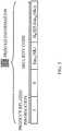
- FIG. 2is a block diagram for illustrating a configuration of the printed information according to the first embodiment of the present invention.
- the printed information 103 and the printed information 106are each formed of the product-related information I and the security code.
- the security code in this caseis formed of the following three pieces of information.
- FIG. 3is a flowchart for illustrating a series of processing to be performed between the control terminal and the master device according to the first embodiment of the present invention.
- a descriptionis given of the operation to be performed between the control terminal 108 and the master device 101.
- the SoC 102activates a key reconstruction function of the FE, which is to be performed by the PUF within the SoC. Specifically, the SoC 102 uses the auxiliary data S, which is a part of the printed information, to reconstruct the secret key K as follows (Step S303). K ⁇ Rep(W', S)
- the SoC 102uses the reconstructed K to calculate the keyed hash value based on the printed information (Step S304). Specifically, the SoC 102 calculates H K (I ⁇ S ⁇ Enc K (MK)), and verifies whether or not there is a match between the calculated value and the keyed hash value of the printed information (Step S305).
- the SoC 102uses the secret key K to decrypt Enc K (MK), which is a part of the printed information, to thereby reconstruct MK (Step S307), and the master device 101 transmits a notification of a successful termination to the control terminal 108 (Step S308). Then, the series of processing is completed.
- MKdecrypt Enc K
- Processing similar to the one for the master device 101is also performed on the slave device 104.
- the slave device 104communicates to and from the control terminal 108 via the master device 101.
- FIG. 4is a flowchart for illustrating a series of processing to be performed between the server and the master device according to the first embodiment of the present invention. Now, a description is given with reference to FIG. 4 .
- the purchaser of the deviceuses the control terminal 108 to transmit the product-related information I to the server 110 via the network, and makes a request for the service (Step S401).
- the server 110transmits a random number R to the master device 101 via the control terminal 108 (Step S402).
- the server 110decrypts the received Enc MK (I ⁇ R) with the use of MK (Step S404), and verifies whether or not there is a match of I and R (Step S405). When it is verified that there is a match, the server 110 registers the service request from the product-related information I in a database as a log (Step S406), and starts providing the service (Step S407). On the other hand, when it is verified that there is a mismatch, the server 110 does not provide the service, but issues an error notification to the service request (Step S408).
- Processing similar to the one for the master device 101is also performed on the slave device 104.
- the slave device 104communicates to and from the control terminal 108 via the master device 101.
- Examples of the service to be provided by the server 110include updating of a program and parameter of the device, and notification of maintenance timing.
- Service information or a part thereofis provided in a form in which the service information is encrypted with the use of the secret information MK, or in such a form as to enable detection of tampering.
- the devicecan receive a secure service by performing decryption and detection of tampering with the use of MK held therein.
- the common key MKis used to perform the authentication between the server 110 and the control terminal 108.
- an equivalent functioncan be achieved with a public key cryptosystem using a pair of public keys (SK, PK).
- FIG. 5is a block diagram for illustrating a configuration of printed information to be adopted in the public key cryptosystem according to the first embodiment of the present invention.
- Enc K (SK)is used in place of Enc K (MK) as the printed information
- H K (I ⁇ S ⁇ Enc K (SK))is used in place of H K (I ⁇ S ⁇ Enc K (MK)) as the keyed hash value.
- the server 110uses the public key PK to determine whether or not the service can be provided. In this way, when the public key cryptosystem is adopted, the burden of information management on the authenticator's side can be alleviated.
- the master device 101encrypts MK with the use of the generated K, and outputs S and Enc K (MK) to the outside. At this time, the SoC does not output K.
- the SoCcalculates, as the security code, H K (I ⁇ S ⁇ Enc K (MK)) in addition to S and Enc K (MK), and outputs the calculated security code to the outside.
- the manufacturercan calculate the keyed hash value by receiving S from the SoC.
- the maintenance persontransmits I and S to the server 110, and makes a printed information reissuance request (Step S601).
- the server 110adds, to the product-related information I, information such as execution of maintenance, a date of maintenance, and the maintenance person as information identifiable to the server, to thereby change the product information I to I' (Step S602).
- the maintenancecan be performed without revealing the secret information MK to the maintenance person, and hence it is possible to reduce a threat to this system.
Landscapes
- Engineering & Computer Science (AREA)
- Computer Security & Cryptography (AREA)
- Computer Networks & Wireless Communication (AREA)
- Signal Processing (AREA)
- Physics & Mathematics (AREA)
- General Physics & Mathematics (AREA)
- Theoretical Computer Science (AREA)
- Storage Device Security (AREA)
Description
- The present invention relates to a device authenticity determination system and device authenticity determination method for detecting a counterfeit product or tampering of a built-in device having a semiconductor chip mounted thereon.
- In recent years, as more built-in devices represented by mobile phones are becoming subjected to networking, the built-in device is increasingly demanded to perform processing involving information security in order to maintain concealment of data handled by the built-in device and integrity thereof, and authenticate the built-in device itself.
- Such processing involving the information security is implemented by an encryption algorithm or an authentication algorithm. Now, consideration is given to a system in which two LSIs perform authentication to confirm that one device to which the other device is connected is valid. As a specific example thereof, there is a conceivable case where an LSI mounted on a mobile phone main body authenticates an LSI mounted on a battery thereof to confirm that the battery is allowed to be connected thereto. That is, the main body to be used as the master verifies the validity and genuineness of the peripheral devices that are to be slaves.
- In general, such a function is implemented by an authentication protocol using encryption. An example of two authentication protocols that differ in encryption scheme is described below.
- (1) A secret key MK is stored in advance in an LSI mounted on a slave A. Further, the secret key MK of the slave A is also registered in a master B.
- (2) At the time of authentication, the master B generates a random number r, encrypts the random number r with the use of the secret key MK to generate c, and transmits the generated c to the slave A. The generated c in this case is represented by c=EMK(r).
- (3) The slave A decrypts c with the use of MK to obtain r', and sends r' to the master B. The generated r' in this case is represented by r'=DMK(c).
- (4) When r=r', the master B issues a notification that the slave A is a genuine product. When r≠r', the master B issues a notification that the slave A may be a counterfeit product.
- It is a point of this protocol that the authentication can be successfully passed as long as the master and the slave each have the same secret key MK.
- (1) A secret key SK is stored in advance in an LSI mounted on a slave A. Further, a public key PK corresponding to the secret key MK of the slave A is also registered in a master B.
- (2) At the time of authentication, the master B generates a random number r, encrypts the random number r with the use of the public key PK to generate c, and transmits the generated c to the slave A. The generated c in this case is represented by c=EPK(r).
- (3) The slave A decrypts c with the use of SK to obtain r', and sends r' to the master B. The generated r' in this case is represented by r'=DSK(c).
- (4) When r=r', the master B issues a notification that the slave A is a genuine product. When r≠r', the master B issues a notification that the slave A may be a counterfeit product.
- It is a point of this protocol that the authentication can be successfully passed as long as the slave has the secret key SK corresponding to the public key PK registered in the master. It is a major premise in executing those protocols that the slave A "securely" holds the secret key MK or SK. The word "securely" means that it is difficult for a person who is not legitimately allowed to access the device to read or tamper with the secret key.
- As a method of securely holding the secret information, there is a technology called a physical unclonable function (PUF). One of major features of the PUF resides in that the secret key K is not held within the device as non-volatile digital data.
- There are several embodiments of such a PUF. "Signal generator based device security" disclosed in Patent Literature 1 and a "semiconductor device identifier generation method and semiconductor device" disclosed in Patent Literature 2 are representative examples of such embodiments.
- Now, secret key generation to be performed by the PUF is briefly described. As the secret key generation to be performed by the PUF, there is known a method using a fuzzy extractor (hereinafter abbreviated as "FE"). Processing procedures to be performed by the FE are shown in tables below as an algorithm 1 and an algorithm 2.
[Table 1] Algorithm 1: Key Generation Processing Gen to be performed by FE Setting: (n,k,2t+1) error correction codeC, general-purpose hash functionhA Input:l·n-bit PUF responseW = (w1,w2,···,wl). Output: (K,S) ←Gen(W), u-bit keyK, l·n-bit auxiliary dataS = (s1,s2,···,sl) 1:i = 1 tol do 2: generate k-bit random numberri 3:ci ←EncodeC (ri) 4:si ←wi ⊕ci 5: end for 6:K ←hA(w1,w2,···,wl) 7: returnK, S Algorithm 2: Key Reconstruction Processing Rep to be performed by FE Setting: (n,k,2t+1) error correction codeC, general-purpose hash functionhA Input:l·n -bit PUF responseW' = (w'1,w'2,···,w'l),l·n -bit auxiliary dataS = (s1,s2,···,sl). Output:K ←Rep(W',S), u-bit keyK. 1:i = 1 tol do 2:c'i ←w'i⊕si 3:ci ←DecodeC(c'i) 4:wi ←ci⊕si 5: end for 6:K ←hA(w1,w2,···,wl) 7: returnK, S - The algorithm 1 is processing of generating a key corresponding to an initial key for the FE, and the key reconstruction processing of the algorithm 2 is processing of generating the same bit string as that of the initial key.
- EncodeC and DecodeC of the algorithm 1 and the algorithm 2 represent encoding processing and correction processing within the error correction code C, respectively. A match between the generated key and the reconstructed key is guaranteed by Expression (1) in terms of a Hamming distance of a PUF response within the algorithm 1 and the algorithm 2.

- Further, when an information amount between chips held by a k-bit PUF output is represented by k', Expression (2) is an appropriate design parameter.

- TUYL P ET AL: "Strong authentication with physical unclonable functions", 1 January 2007 (2007-01-01), SECURITY, PRIVACY, AND TRUST IN MODERN DATA MANAGEMENT :WITH 13 TABLES, SPRINGER, BERLIN, DE, PAGE(S) 133 - 148, XP009139190, ISBN: 978-3-540-69860-9 refers to strong authentication with physical unclonable functions. Physical unclonable functions (PUFs) can be used as a cost-effective means to store cryptographic key material in an unclonable way. They can be employed for strong authentication of objects, e. g., tokens, and of persons possessing such tokens, but also for other purposes. A short overview of security applications is given where PUFs are useful, and physical realisations, noisy measurements and information content of PUFs are discussed. Then it is described an integrated authentication token containing an optical PUF, a challenging mechanism and a detector. Finally, authentication protocols for controlled and uncontrolled PUFs are discussed.
- JORGE GUAJARDO ET AL: "Anti-counterfeiting, key distribution, and key storage in an ambient world via physical unclonable functions", INFORMATION SYSTEMS FRONTIERS; A JOURNAL OF RESEARCH AND INNOVATION, KLUWER ACADEMIC PUBLISHERS, BO, vol. 11, no. 1, 23 October 2008 (2008-10-23), pages 19-41, XP019677732, ISSN: 1572-9419 refers to anti-counterfeiting, key distribution, and key storage in an ambient world via physical unclonable functions.
- PIM TUYLS ET AL: "RFID-Tags for Anti-counterfeiting", 1 January 2005 (2005-01-01), TOPICS IN CRYPTOLOGY - CT- RSA 2006 : THE CRYPTOGRAPHERS' TRACK AT THE RSA CONFERENCE 2006, SAN JOSE, CA, USA, FEBRUARY 13-17, 2006 ; PROCEEDINGS; [LECTURE NOTES IN COMPUTER SCIENCE], SPRINGER; BERLIN, DE, PAGE(S) 115-131, XP019026798, ISBN: 978-3-540-31033-4 refers to RFID-tags for anti-counterfeiting.
- [PTL 1]
JP 2009-524998 A1 - [PTL 2]
JP 2009-533741 A1 - However, the related arts have the following problems.
- The above-mentioned authentication protocol does not essentially verify the authenticity of the entire built-in device A, but performs the authentication on the LSI incorporated into the built-in device A. Accordingly, for example, this authentication protocol cannot detect a counterfeit product produced by taking out the LSI of the genuine product that has been discarded once or an electronic board having the LSI mounted thereon and replacing other components such as a casing with new components.
- Moreover, for a reason such as use of common components for achieving compatibility or cost reduction, when the same LSI or the electronic board having this LSI mounted thereon is used in two types of models including built-in devices A1 and A2, the above-mentioned authentication protocol cannot detect such an illicit action that the component of the model A1, which is less expensive, is altered to construct the model A2, which is more expensive.
- The counterfeit product or illicit product produced by those illicit actions may not be capable of achieving a function and performance intrinsic to the genuine product, and hence such a product may cause a trouble or an accident.
- Those problems occur because, although a user of the built-in device can verify the device from the exterior of the device such as a package or a casing, it is difficult for the user to detect a mismatch or inconsistency in terms of an internal configuration of the device. A conceivable cause of such problems is that, although the user of the built-in device can verify information printed on the exterior of the device such as the package or the casing visually or the like, it is difficult for the user to verify whether or not the inside of the built-in device is genuine.
- The present invention has been made in view of the above-mentioned problems, and has an object to provide a device authenticity determination system and device authenticity determination method, which enable verification as to whether or not there is a match between an LSI mounted on a built-in device or an electronic board having the LSI mounted thereon and information printed on a casing that is viewable from a user of the built-in device.
- According to one embodiment of the present invention, there is provided a device authenticity determination system for using printed information, which is viewable from an exterior of a device or a component, the device and component having mounted thereon a semiconductor chip having a PUF function and an encryption function, and includes auxiliary data, for generating secret information being difficult to duplicate with use of the PUF function, and the secret information, the device authenticity determination system comprising a control terminal for reading the printed information, which is viewable, and transmitting the printed information to the semiconductor chip through electronic access means, in which the semiconductor chip further has a tampering determination function of temporarily reconstructing, through the encryption function and the PUF function, the secret information being difficult to duplicate with use of the auxiliary data included in the printed information acquired from the control terminal, performing comparison processing between the secret information included in the printed information and the temporarily-reconstructed secret information being difficult to duplicate, and determining that tampering has occurred when detecting a mismatch between the secret information included in the printed information and the temporarily-reconstructed secret information being difficult to duplicate.
- Further, according to one embodiment of the present invention, there is provided a device authenticity determination method to be used for a device authenticity determination system for using printed information, which is viewable from an exterior of a device or a component, the device and the component having mounted thereon a semiconductor chip having a PUF function and an encryption function, and includes auxiliary data, for generating secret information being difficult to duplicate with use of the PUF function, and the secret information, the device authenticity determination method including the steps of: reading, by the control terminal, the printed information, which is viewable, and transmitting the printed information to the semiconductor chip through electronic access means; temporarily reconstructing, by the semiconductor chip, the secret information being difficult to duplicate with use of the auxiliary data included in the printed information acquired from the control terminal; and performing, by the semiconductor chip, comparison processing between the secret information included in the printed information and the temporarily-reconstructed secret information being difficult to duplicate, and determining that tampering has occurred when detecting a mismatch between the secret information included in the printed information and the temporarily-reconstructed secret information being difficult to duplicate.
- According to the one embodiment of the present invention, through the determination as to whether or not there is a match between the printed information attached to the casing of the built-in device having the semiconductor chip mounted thereon and the printed information generated by the currently-mounted semiconductor chip based on the result of reading the printed information, it is possible to provide the device authenticity determination system and device authenticity determination method, which enable the verification as to whether or not there is a match between the LSI mounted on the built-in device or the electronic board having the LSI mounted thereon and the information printed on the casing that is viewable from the user of the built-in device.
FIG. 1 is an overall configuration diagram of a device authenticity determination system according to a first embodiment of the present invention.FIG. 2 is a block diagram for illustrating a configuration of printed information according to the first embodiment of the present invention.FIG. 3 is a flowchart for illustrating a series of processing to be performed between a control terminal and a master device according to the first embodiment of the present invention.FIG. 4 is a flowchart for illustrating a series of processing to be performed between a server and the master device according to the first embodiment of the present invention.FIG. 5 is a block diagram for illustrating a configuration of printed information to be adopted in a public key cryptosystem according to the first embodiment of the present invention.FIG. 6 is a flowchart for illustrating a series of processing to be performed at the time of maintenance according to a second embodiment of the present invention.FIG. 7 is a block diagram for illustrating a configuration of printed information after a change according to the second embodiment of the present invention.- Now, a description is given of a device authenticity determination system and a device authenticity determination method according to preferred embodiments of the present invention with reference to the drawings.
FIG. 1 is an overall configuration diagram of a device authenticity determination system according to a first embodiment of the present invention. Amaster device 101 has a system on chip (SoC) 102, which is a main constituent element of the device, and theSoC 102 has a PUF function and an encryption function. Further, themaster device 101 has printedinformation 103 on its casing. The printed information includes, in addition to general product-related information I such as a model number, rating, manufacture date, and serial number of the device, a security code, which is a point of the present invention. The printed information is printed in a form of a QR code (trademark) or a barcode, for example.- Similarly, a
slave device 104 has anSoC 105 and printedinformation 106, and is connected to themaster device 101 via acommunication channel 107. Themaster device 101 is connected to acontrol terminal 108 via acommunication channel 109, and theslave device 104 is connected to thecontrol terminal 108 via thecommunication channel 107, themaster device 101, and thecommunication channel 109. - Such connections enable the
control terminal 108 to make necessary settings of themaster device 101 and theslave device 104. In this case, a device such as a PC or a tablet computer is assumed as thecontrol terminal 108. Further, thecontrol terminal 108 is connected to aserver 110 via the Internet. Note that, in the following, when what is common to both of themaster device 101 and theslave device 104 is described, those devices are each simply referred to as "device". FIG. 2 is a block diagram for illustrating a configuration of the printed information according to the first embodiment of the present invention. The printedinformation 103 and the printedinformation 106 are each formed of the product-related information I and the security code. The security code in this case is formed of the following three pieces of information.- Auxiliary data S, which is output from the PUF of the SoC mounted on the device to which the printed information is attached.
- Data EncK(MK), which is obtained by encrypting a master key MK with the use of secret information K, which is generated by the PUF in a manner that corresponds to the auxiliary data S.
- A keyed hash value HK(I∥S∥EncK(MK)) having K as a key, which is generated based on a concatenated data string of I, S, and EncK(MK). Note that, the HMAC method can be given as an example of calculation of the keyed hash value. In this case, "∥" means concatenation of bits.
- Next, a description is given of an operation of the device authenticity determination system according to the first embodiment having the configuration illustrated in
FIG. 1 .FIG. 3 is a flowchart for illustrating a series of processing to be performed between the control terminal and the master device according to the first embodiment of the present invention. First, with reference toFIG. 3 , a description is given of the operation to be performed between thecontrol terminal 108 and themaster device 101. - A purchaser of the device inputs the printed
information 103 to the control terminal 108 (Step S301). Next, the printed information is transmitted from thecontrol terminal 108 to the master device 101 (Step S302). TheSoC 102 of themaster device 101 reconstructs the key MK from the transmitted printed information through the following procedure. - The
SoC 102 activates a key reconstruction function of the FE, which is to be performed by the PUF within the SoC. Specifically, theSoC 102 uses the auxiliary data S, which is a part of the printed information, to reconstruct the secret key K as follows (Step S303).
K←Rep(W', S) - Next, the
SoC 102 uses the reconstructed K to calculate the keyed hash value based on the printed information (Step S304). Specifically, theSoC 102 calculates HK(I∥S∥EncK(MK)), and verifies whether or not there is a match between the calculated value and the keyed hash value of the printed information (Step S305). - In Step S305, when a match between the values cannot be verified, the
master device 101 transmits a notification that there is no match to the control terminal 108 (Step S306), and interrupts the processing. On the other hand, when a match between the values can be verified, the processing proceeds to the next step, which is Step S307. - Finally, the
SoC 102 uses the secret key K to decrypt EncK(MK), which is a part of the printed information, to thereby reconstruct MK (Step S307), and themaster device 101 transmits a notification of a successful termination to the control terminal 108 (Step S308). Then, the series of processing is completed. - Processing similar to the one for the
master device 101 is also performed on theslave device 104. Note that, theslave device 104 communicates to and from thecontrol terminal 108 via themaster device 101. - When the printed information does not correspond to the SoC (102, 105) of the device, the true K cannot be reconstructed due to the property of the PUF. Accordingly, there occurs a mismatch with the keyed hash value written as the printed information, which enables the detection of an illicit product.
- Next, a description is given of an operation to be performed between the
master device 101 and theserver 110 via thecontrol terminal 108. This operation is performed in order that the purchaser of the device, who has the genuine product, receives an appropriate service for the device from a manufacturer. - As described above in the operation of
FIG. 3 , when the purchaser's device is the genuine product, a state in which the correct MK is reconstructed in the SoC is reached. Further, MK is information set by the manufacturer, and theserver 110 holds the correct MK. Accordingly, if the purchaser's device is the genuine product, at the time when the operation illustrated inFIG. 3 is finished, a state in which the device and theserver 110 share the same key is reached. FIG. 4 is a flowchart for illustrating a series of processing to be performed between the server and the master device according to the first embodiment of the present invention. Now, a description is given with reference toFIG. 4 . The purchaser of the device uses thecontrol terminal 108 to transmit the product-related information I to theserver 110 via the network, and makes a request for the service (Step S401). Theserver 110 transmits a random number R to themaster device 101 via the control terminal 108 (Step S402).- The
master device 101 encrypts the product-related information I, which is transmitted to within the SoC in Step S302, and the random number R with the use of MK, and transmits the resultant data to theserver 110 via the control terminal 108 (Step S403). Specifically, themaster device 101 transmits EncMK(I∥R). - The
server 110 decrypts the received EncMK(I∥R) with the use of MK (Step S404), and verifies whether or not there is a match of I and R (Step S405). When it is verified that there is a match, theserver 110 registers the service request from the product-related information I in a database as a log (Step S406), and starts providing the service (Step S407). On the other hand, when it is verified that there is a mismatch, theserver 110 does not provide the service, but issues an error notification to the service request (Step S408). - Processing similar to the one for the
master device 101 is also performed on theslave device 104. Note that, theslave device 104 communicates to and from thecontrol terminal 108 via themaster device 101. - Examples of the service to be provided by the
server 110 include updating of a program and parameter of the device, and notification of maintenance timing. Service information or a part thereof is provided in a form in which the service information is encrypted with the use of the secret information MK, or in such a form as to enable detection of tampering. The device can receive a secure service by performing decryption and detection of tampering with the use of MK held therein. - In the above description of the first embodiment, the common key MK is used to perform the authentication between the
server 110 and thecontrol terminal 108. On the other hand, as described above in the "Background Art" section, an equivalent function can be achieved with a public key cryptosystem using a pair of public keys (SK, PK). FIG. 5 is a block diagram for illustrating a configuration of printed information to be adopted in the public key cryptosystem according to the first embodiment of the present invention. As compared with the above-mentioned configuration of the printed information to be adopted in the common key cryptosystem illustrated inFIG. 2 , in the configuration ofFIG. 5 , EncK(SK) is used in place of EncK(MK) as the printed information, and HK(I∥S∥EncK(SK)) is used in place of HK(I∥S∥EncK(MK)) as the keyed hash value. Further, theserver 110 uses the public key PK to determine whether or not the service can be provided. In this way, when the public key cryptosystem is adopted, the burden of information management on the authenticator's side can be alleviated.- In a second embodiment of the present invention, a description is given of a case where easiness in changing of the printed information is considered. The manufacturer inputs, to the
master device 101, the product-related information I and the secret key MK that are scheduled to be printed on the casing, and causes themaster device 101 to execute the following key generation processing.
(K, S)←Gen(W) - The
master device 101 encrypts MK with the use of the generated K, and outputs S and EncK(MK) to the outside. At this time, the SoC does not output K. - In the format of the printed information of
FIG. 2 according to the first embodiment described above, the SoC calculates, as the security code, HK(I∥S∥EncK(MK)) in addition to S and EncK(MK), and outputs the calculated security code to the outside. However, in the second embodiment, the manufacturer can calculate the keyed hash value by receiving S from the SoC. FIG. 6 is a flowchart for illustrating a series of processing to be performed at the time of maintenance according to the second embodiment of the present invention. In this case, maintenance that does not involve a change of the SoC is assumed. Note that, maintenance involving a change of the SoC, namely, maintenance corresponding to replacement of the device, is performed based on the same flow as the one performed at the time of manufacture.- After finishing repairing the device, a maintenance person requests, via the control terminal, the service illustrated in Step S406 of
FIG. 4 from theserver 110. At this time, it is assumed that the device has transitioned to a state in which the device holds MK within the SoC in accordance with the flowchart ofFIG. 3 . It is also assumed that theserver 110 can separately verify the authenticity of the maintenance person in accordance with general access control. - The maintenance person transmits I and S to the
server 110, and makes a printed information reissuance request (Step S601). In response to this request, theserver 110 adds, to the product-related information I, information such as execution of maintenance, a date of maintenance, and the maintenance person as information identifiable to the server, to thereby change the product information I to I' (Step S602). - Further, the
server 110 uses the changed I' and S, and MK held by the server to calculate HMK(I'∥S∥MK), and transmits I' and HMK(I'∥S∥MK) to the maintenance person (Step S603). FIG. 7 is a block diagram for illustrating a configuration of the printed information after the change according to the second embodiment of the present invention. The maintenance person generates the printed information in a format illustrated inFIG. 7 , and reprints the information on the casing by replacing a current sticker with a new sticker, for example (Step S604).- As described above, through the series of processing of the flowchart illustrated in
FIG. 6 , the maintenance can be performed without revealing the secret information MK to the maintenance person, and hence it is possible to reduce a threat to this system.


Claims (9)
- A device authenticity determination system for using a semiconductor chip (102) having a PUF function and for using printed information (103), the printed information (103) is viewable from an exterior of a device (101) or a component, the device (101) and the component having mounted thereon the semiconductor chip (102), and the printed information (103) includes auxiliary data, for generating secret information with use of the PUF function, data obtained by encrypting a master key with the use of the secret information, and keyed hash value calculated with the use of the master key as a key against a concatenated data including the auxiliary data and product related information included in said printed information and the encrypted data,
the device authenticity determination system comprising a control terminal (108) for reading the printed information (103), which is viewable, and transmitting the printed information (103) to the semiconductor chip (102) through electronic access means,
wherein the semiconductor chip (102) further has a confirmation function of temporarily reconstructing, through the PUF function, the secret information with use of the auxiliary data included in the printed information (103) acquired from the control terminal (108), calculating keyed hash value against the concatenated data included in the printed information (103) with use of the temporarily-reconstructed secret information, and confirming whether or not there is a match between the keyed hash value included in the printed information (103) and the keyed hash value calculated with the use of the temporarily-reconstructed secret information. - A device authenticity determination system according to claim 1,
wherein the printed information (103) further comprises information obtained by protecting second secret information set by a manufacturer of the device (101) or the component with use of the secret information being difficult to duplicate, and
wherein, through the PUF function, the semiconductor chip (102) reconstructs the second secret information after reconstructing the secret information, and through the confirmation function, the semiconductor chip (102) confirms whether or not there is a match between the second secret information set by the manufacturer and the reconstructed second secret information. - A device authenticity determination system according to claim 2, wherein the semiconductor chip (102) verifies appropriateness of the reconstructed second secret information through hash calculation for determining appropriateness.
- A device authenticity determination system according to claim 2, further comprising a server (110) connected to the control terminal (108) via a network,
wherein the semiconductor chip (102) transmits, through the control terminal (108), the reconstructed second secret information to the server (110) via the network, and
wherein the server (110) compares the second secret information reconstructed by the semiconductor chip (102) with second secret information held by itself to verify validity of the device (101) or the component having the semiconductor chip (102) mounted thereon, and after verifying the validity when a comparison result indicates a match between the second secret information reconstructed by the semiconductor chip (102) and the second secret information held by itself, provides service information to the device (101) or the component. - A device authenticity determination system according to claim 4,
wherein the server (110) encrypts the service information with use of the second secret information, and transmits the encrypted service information, and
wherein the semiconductor chip (102) that has transmitted the reconstructed second secret information acquires the service information encrypted with use of the second secret information, and decrypts the service information with use of the second secret information reconstructed by itself, to thereby acquire the service information from the server (110) . - A device authenticity determination system according to claim 4 or 5,
wherein based on an operation of a maintenance person, the control terminal (108) transmits a printed information (103) reissuance request comprising the auxiliary data to the server (110),
wherein when receiving the printed information (103) reissuance request from the control terminal (108), the server (110) uses the second secret information to generate new printed information (103) to which maintenance information is added, and returns the generated new printed information (103) to the control terminal (108) that has transmitted the printed information (103) reissuance request, and
wherein the control terminal (108) reprints the new printed information (103) in order that the printed information (103), which is viewable, is updated with the received new printed information - A built-in device system according to any of claims 1 to 5 wherein said semiconductor chip further has a confirmation function of acquiring the printed information through electronic access means.
- A device authenticity determination method to be used for a device authenticity determination system for using a semiconductor chip (102) having a PUF function and for using printed information (103), the printed information (103) is viewable from an exterior of a device (101) or a component, the device (101) and the component having mounted thereon the semiconductor chip (102), and the printed information (103) includes auxiliary data, for generating secret information with use of the PUF function, data obtained by encrypting a master key with the use of the secret information, and keyed hash value calculated with the use of the master key as a key against a concatenated data including the auxiliary data and product related information included in said printed information and the encrypted data,
the device authenticity determination method including the steps of:reading, by a control terminal (108), the printed information (103), which is viewable, and transmitting the printed information (103) to the semiconductor chip (102) through electronic access means;temporarily reconstructing, by the semiconductor chip (102), the secret information with use of the auxiliary data included in the printed information (103) acquired from the control terminal (108); andcalculating, by the semiconductor chip (102), keyed hash value against the concatenated data included in the printed information (103) with use of the temporarily-reconstructed secret information, and confirming whether or not there is a match between the keyed hash value included in the printed information (103) and the keyed hash value calculated with the use of the temporarily-reconstructed secret information. - A built-in device having a semiconductor chip mounted thereon comprising the semiconductor chip (102) according to any of claims 1 to 5; wherein the semiconductor chip (102) further has a confirmation function of
acquiring the printed information through electronic access means.
Applications Claiming Priority (1)
| Application Number | Priority Date | Filing Date | Title |
|---|---|---|---|
| PCT/JP2013/063560WO2014184899A1 (en) | 2013-05-15 | 2013-05-15 | Device authenticity determination system and device authenticity determination method |
Publications (3)
| Publication Number | Publication Date |
|---|---|
| EP2999156A1 EP2999156A1 (en) | 2016-03-23 |
| EP2999156A4 EP2999156A4 (en) | 2017-01-11 |
| EP2999156B1true EP2999156B1 (en) | 2019-07-31 |
Family
ID=51897914
Family Applications (1)
| Application Number | Title | Priority Date | Filing Date |
|---|---|---|---|
| EP13884745.4AActiveEP2999156B1 (en) | 2013-05-15 | 2013-05-15 | Device authenticity determination system and device authenticity determination method |
Country Status (7)
| Country | Link |
|---|---|
| US (1) | US20160080153A1 (en) |
| EP (1) | EP2999156B1 (en) |
| JP (1) | JP5885178B2 (en) |
| KR (1) | KR101752083B1 (en) |
| CN (1) | CN105229965B (en) |
| TW (1) | TWI518548B (en) |
| WO (1) | WO2014184899A1 (en) |
Families Citing this family (19)
| Publication number | Priority date | Publication date | Assignee | Title |
|---|---|---|---|---|
| EP3058694B1 (en)* | 2013-10-15 | 2018-12-12 | Telefonaktiebolaget LM Ericsson (publ) | Establishing a secure connection between a master device and a slave device |
| US10432409B2 (en) | 2014-05-05 | 2019-10-01 | Analog Devices, Inc. | Authentication system and device including physical unclonable function and threshold cryptography |
| US10019604B2 (en) | 2014-10-31 | 2018-07-10 | Xiaomi Inc. | Method and apparatus of verifying terminal and medium |
| CN104484593B (en)* | 2014-10-31 | 2017-10-20 | 小米科技有限责任公司 | terminal verification method and device |
| JP2018507658A (en)* | 2015-03-05 | 2018-03-15 | アナログ ディヴァイスィズ インク | Authentication system and device including physically non-replicatable function and threshold encryption |
| CN107710675A (en)* | 2015-06-22 | 2018-02-16 | 三菱电机株式会社 | Authenticity determining device and authenticating method |
| EP3340213B1 (en)* | 2016-12-21 | 2020-03-11 | Merck Patent GmbH | Puf based composite security marking for anti-counterfeiting |
| ES2764128T3 (en)* | 2016-12-21 | 2020-06-02 | Merck Patent Gmbh | Reading device to read a composite mark that includes a non-clonal physical function to fight counterfeiting |
| US10958452B2 (en) | 2017-06-06 | 2021-03-23 | Analog Devices, Inc. | System and device including reconfigurable physical unclonable functions and threshold cryptography |
| IL256108B (en) | 2017-12-04 | 2021-02-28 | Elbit Systems Ltd | System and method for detecting usage condition and authentication of an article of manufacture |
| EP3564846A1 (en)* | 2018-04-30 | 2019-11-06 | Merck Patent GmbH | Methods and systems for automatic object recognition and authentication |
| EP3565179B1 (en)* | 2018-04-30 | 2022-10-19 | Merck Patent GmbH | Composite security marking and methods and apparatuses for providing and reading same |
| US11151290B2 (en) | 2018-09-17 | 2021-10-19 | Analog Devices, Inc. | Tamper-resistant component networks |
| US20230037023A1 (en)* | 2020-01-23 | 2023-02-02 | Tokyo University Of Science Foundation | Registration Device, Verification Device, Identification Device, and Individual Identification System |
| KR102334005B1 (en)* | 2020-04-24 | 2021-12-02 | (주)메티스 | Gateway module having PUF based on CC-LINK |
| KR102340585B1 (en)* | 2020-04-24 | 2021-12-20 | (주)메티스 | Slave module having PUF based on CC-LINK |
| US11917088B2 (en)* | 2020-09-21 | 2024-02-27 | International Business Machines Corporation | Integrating device identity into a permissioning framework of a blockchain |
| DE102021105402A1 (en)* | 2021-03-05 | 2022-09-08 | Infineon Technologies Ag | DATA PROCESSING DEVICE AND METHOD FOR TRANSMITTING DATA VIA A BUS |
| CN113872769B (en)* | 2021-09-29 | 2024-02-20 | 天翼物联科技有限公司 | Device authentication method and device based on PUF, computer device and storage medium |
Family Cites Families (20)
| Publication number | Priority date | Publication date | Assignee | Title |
|---|---|---|---|---|
| US5960086A (en)* | 1995-11-02 | 1999-09-28 | Tri-Strata Security, Inc. | Unified end-to-end security methods and systems for operating on insecure networks |
| JPH09284272A (en)* | 1996-04-19 | 1997-10-31 | Canon Inc | Encryption method based on entity attribute information, signature method, key sharing method, identity verification method and device for these methods |
| US20030145208A1 (en)* | 2002-01-25 | 2003-07-31 | Willins Bruce A. | System and method for improving integrity and authenticity of an article utilizing secure overlays |
| US7840803B2 (en)* | 2002-04-16 | 2010-11-23 | Massachusetts Institute Of Technology | Authentication of integrated circuits |
| JP2004072214A (en)* | 2002-08-02 | 2004-03-04 | Sharp Corp | Electronic seals, IC cards, personal identification systems and portable devices |
| JP2006040190A (en)* | 2004-07-30 | 2006-02-09 | Omron Corp | Communication system, communication device and method, working apparatus and method, recording medium, and program |
| JP4691346B2 (en)* | 2004-10-08 | 2011-06-01 | 株式会社エルイーテック | Semiconductor device for gaming machine control, and inspection apparatus and inspection method therefor |
| GB0503972D0 (en)* | 2005-02-25 | 2005-04-06 | Firstondemand Ltd | Identification systems |
| JP2009508430A (en)* | 2005-09-14 | 2009-02-26 | コーニンクレッカ フィリップス エレクトロニクス エヌ ヴィ | Device, system and method for determining authenticity of items |
| US8224018B2 (en)* | 2006-01-23 | 2012-07-17 | Digimarc Corporation | Sensing data from physical objects |
| TWI416921B (en) | 2006-01-24 | 2013-11-21 | Pufco Inc | Method,integrated circuit,and computer program product for signal generator based device security |
| KR101059005B1 (en) | 2006-04-13 | 2011-08-23 | 엔엑스피 비 브이 | Semiconductor device, identifier generation method and identification method thereof |
| US8334757B2 (en)* | 2006-12-06 | 2012-12-18 | Koninklijke Philips Electronics N.V. | Controlling data access to and from an RFID device |
| US20100177898A1 (en)* | 2007-06-14 | 2010-07-15 | Intrinsic Id Bv | Device and method for providing authentication |
| US8549298B2 (en)* | 2008-02-29 | 2013-10-01 | Microsoft Corporation | Secure online service provider communication |
| WO2009156904A1 (en)* | 2008-06-27 | 2009-12-30 | Koninklijke Philips Electronics N.V. | Device, system and method for verifying the authenticity integrity and/or physical condition of an item |
| JP2010108054A (en)* | 2008-10-28 | 2010-05-13 | Mitsubishi Electric Corp | Authentication system, authentication method, authentication program, authentication apparatus, and request device |
| JP5499358B2 (en)* | 2010-03-24 | 2014-05-21 | 独立行政法人産業技術総合研究所 | Authentication processing method and apparatus |
| JP5420114B2 (en)* | 2011-06-02 | 2014-02-19 | 三菱電機株式会社 | Key information generating apparatus and key information generating method |
| US20130087609A1 (en)* | 2011-06-17 | 2013-04-11 | The University of Washington through its Center for Commercialization, a public Institution of Hig | Medical Device Tracking System and Method |
- 2013
- 2013-05-15CNCN201380076598.6Apatent/CN105229965B/enactiveActive
- 2013-05-15USUS14/785,805patent/US20160080153A1/ennot_activeAbandoned
- 2013-05-15EPEP13884745.4Apatent/EP2999156B1/enactiveActive
- 2013-05-15JPJP2015516815Apatent/JP5885178B2/enactiveActive
- 2013-05-15WOPCT/JP2013/063560patent/WO2014184899A1/enactiveApplication Filing
- 2013-05-15KRKR1020157035359Apatent/KR101752083B1/enactiveActive
- 2013-09-24TWTW102134235Apatent/TWI518548B/enactive
Non-Patent Citations (1)
| Title |
|---|
| None* |
Also Published As
| Publication number | Publication date |
|---|---|
| WO2014184899A1 (en) | 2014-11-20 |
| CN105229965A (en) | 2016-01-06 |
| JPWO2014184899A1 (en) | 2017-02-23 |
| TWI518548B (en) | 2016-01-21 |
| US20160080153A1 (en) | 2016-03-17 |
| EP2999156A4 (en) | 2017-01-11 |
| KR101752083B1 (en) | 2017-06-28 |
| JP5885178B2 (en) | 2016-03-15 |
| TW201443689A (en) | 2014-11-16 |
| CN105229965B (en) | 2018-10-09 |
| KR20160010521A (en) | 2016-01-27 |
| EP2999156A1 (en) | 2016-03-23 |
Similar Documents
| Publication | Publication Date | Title |
|---|---|---|
| EP2999156B1 (en) | Device authenticity determination system and device authenticity determination method | |
| US11811912B1 (en) | Cryptographic algorithm status transition | |
| US20240354756A1 (en) | Transaction messaging | |
| US11888974B1 (en) | Secret sharing information management and security system | |
| US11074349B2 (en) | Apparatus with anticounterfeiting measures | |
| CN111080295B (en) | Electronic contract processing method and device based on blockchain | |
| CN101765996A (en) | Remote Authentication and Transaction Signing | |
| US10547451B2 (en) | Method and device for authentication | |
| CN111127014B (en) | Transaction information processing method, server, user terminal, system and storage medium | |
| CN117857060B (en) | Two-dimensional code offline verification method, system and storage medium | |
| CN114499825B (en) | Dual-control key management method, system, encryption machine and storage medium | |
| CN108199847A (en) | Security processing method, computer equipment and storage medium | |
| CN119768815A (en) | Carbon data management method, device, system and related equipment | |
| Oliveira | Dynamic QR codes for Ticketing Systems | |
| CN115134093A (en) | Digital signature method and computing device |
Legal Events
| Date | Code | Title | Description |
|---|---|---|---|
| PUAI | Public reference made under article 153(3) epc to a published international application that has entered the european phase | Free format text:ORIGINAL CODE: 0009012 | |
| 17P | Request for examination filed | Effective date:20151116 | |
| AK | Designated contracting states | Kind code of ref document:A1 Designated state(s):AL AT BE BG CH CY CZ DE DK EE ES FI FR GB GR HR HU IE IS IT LI LT LU LV MC MK MT NL NO PL PT RO RS SE SI SK SM TR | |
| AX | Request for extension of the european patent | Extension state:BA ME | |
| DAX | Request for extension of the european patent (deleted) | ||
| A4 | Supplementary search report drawn up and despatched | Effective date:20161209 | |
| RIC1 | Information provided on ipc code assigned before grant | Ipc:H04L 9/10 20060101AFI20161205BHEP Ipc:H04L 9/32 20060101ALI20161205BHEP | |
| STAA | Information on the status of an ep patent application or granted ep patent | Free format text:STATUS: EXAMINATION IS IN PROGRESS | |
| 17Q | First examination report despatched | Effective date:20180618 | |
| REG | Reference to a national code | Ref country code:DE Ref legal event code:R079 Ref document number:602013058646 Country of ref document:DE Free format text:PREVIOUS MAIN CLASS: H04L0009100000 Ipc:G09C0001000000 | |
| GRAP | Despatch of communication of intention to grant a patent | Free format text:ORIGINAL CODE: EPIDOSNIGR1 | |
| STAA | Information on the status of an ep patent application or granted ep patent | Free format text:STATUS: GRANT OF PATENT IS INTENDED | |
| RIC1 | Information provided on ipc code assigned before grant | Ipc:H04L 9/32 20060101ALI20190125BHEP Ipc:G09C 1/00 20060101AFI20190125BHEP Ipc:H04L 9/08 20060101ALI20190125BHEP | |
| INTG | Intention to grant announced | Effective date:20190214 | |
| GRAS | Grant fee paid | Free format text:ORIGINAL CODE: EPIDOSNIGR3 | |
| GRAA | (expected) grant | Free format text:ORIGINAL CODE: 0009210 | |
| STAA | Information on the status of an ep patent application or granted ep patent | Free format text:STATUS: THE PATENT HAS BEEN GRANTED | |
| AK | Designated contracting states | Kind code of ref document:B1 Designated state(s):AL AT BE BG CH CY CZ DE DK EE ES FI FR GB GR HR HU IE IS IT LI LT LU LV MC MK MT NL NO PL PT RO RS SE SI SK SM TR | |
| REG | Reference to a national code | Ref country code:CH Ref legal event code:EP Ref country code:GB Ref legal event code:FG4D | |
| REG | Reference to a national code | Ref country code:AT Ref legal event code:REF Ref document number:1161744 Country of ref document:AT Kind code of ref document:T Effective date:20190815 | |
| REG | Reference to a national code | Ref country code:IE Ref legal event code:FG4D | |
| REG | Reference to a national code | Ref country code:DE Ref legal event code:R096 Ref document number:602013058646 Country of ref document:DE | |
| REG | Reference to a national code | Ref country code:NL Ref legal event code:MP Effective date:20190731 | |
| REG | Reference to a national code | Ref country code:LT Ref legal event code:MG4D | |
| REG | Reference to a national code | Ref country code:AT Ref legal event code:MK05 Ref document number:1161744 Country of ref document:AT Kind code of ref document:T Effective date:20190731 | |
| PG25 | Lapsed in a contracting state [announced via postgrant information from national office to epo] | Ref country code:LT Free format text:LAPSE BECAUSE OF FAILURE TO SUBMIT A TRANSLATION OF THE DESCRIPTION OR TO PAY THE FEE WITHIN THE PRESCRIBED TIME-LIMIT Effective date:20190731 Ref country code:HR Free format text:LAPSE BECAUSE OF FAILURE TO SUBMIT A TRANSLATION OF THE DESCRIPTION OR TO PAY THE FEE WITHIN THE PRESCRIBED TIME-LIMIT Effective date:20190731 Ref country code:SE Free format text:LAPSE BECAUSE OF FAILURE TO SUBMIT A TRANSLATION OF THE DESCRIPTION OR TO PAY THE FEE WITHIN THE PRESCRIBED TIME-LIMIT Effective date:20190731 Ref country code:FI Free format text:LAPSE BECAUSE OF FAILURE TO SUBMIT A TRANSLATION OF THE DESCRIPTION OR TO PAY THE FEE WITHIN THE PRESCRIBED TIME-LIMIT Effective date:20190731 Ref country code:NO Free format text:LAPSE BECAUSE OF FAILURE TO SUBMIT A TRANSLATION OF THE DESCRIPTION OR TO PAY THE FEE WITHIN THE PRESCRIBED TIME-LIMIT Effective date:20191031 Ref country code:NL Free format text:LAPSE BECAUSE OF FAILURE TO SUBMIT A TRANSLATION OF THE DESCRIPTION OR TO PAY THE FEE WITHIN THE PRESCRIBED TIME-LIMIT Effective date:20190731 Ref country code:AT Free format text:LAPSE BECAUSE OF FAILURE TO SUBMIT A TRANSLATION OF THE DESCRIPTION OR TO PAY THE FEE WITHIN THE PRESCRIBED TIME-LIMIT Effective date:20190731 Ref country code:PT Free format text:LAPSE BECAUSE OF FAILURE TO SUBMIT A TRANSLATION OF THE DESCRIPTION OR TO PAY THE FEE WITHIN THE PRESCRIBED TIME-LIMIT Effective date:20191202 Ref country code:BG Free format text:LAPSE BECAUSE OF FAILURE TO SUBMIT A TRANSLATION OF THE DESCRIPTION OR TO PAY THE FEE WITHIN THE PRESCRIBED TIME-LIMIT Effective date:20191031 | |
| PG25 | Lapsed in a contracting state [announced via postgrant information from national office to epo] | Ref country code:RS Free format text:LAPSE BECAUSE OF FAILURE TO SUBMIT A TRANSLATION OF THE DESCRIPTION OR TO PAY THE FEE WITHIN THE PRESCRIBED TIME-LIMIT Effective date:20190731 Ref country code:LV Free format text:LAPSE BECAUSE OF FAILURE TO SUBMIT A TRANSLATION OF THE DESCRIPTION OR TO PAY THE FEE WITHIN THE PRESCRIBED TIME-LIMIT Effective date:20190731 Ref country code:IS Free format text:LAPSE BECAUSE OF FAILURE TO SUBMIT A TRANSLATION OF THE DESCRIPTION OR TO PAY THE FEE WITHIN THE PRESCRIBED TIME-LIMIT Effective date:20191130 Ref country code:GR Free format text:LAPSE BECAUSE OF FAILURE TO SUBMIT A TRANSLATION OF THE DESCRIPTION OR TO PAY THE FEE WITHIN THE PRESCRIBED TIME-LIMIT Effective date:20191101 Ref country code:AL Free format text:LAPSE BECAUSE OF FAILURE TO SUBMIT A TRANSLATION OF THE DESCRIPTION OR TO PAY THE FEE WITHIN THE PRESCRIBED TIME-LIMIT Effective date:20190731 Ref country code:ES Free format text:LAPSE BECAUSE OF FAILURE TO SUBMIT A TRANSLATION OF THE DESCRIPTION OR TO PAY THE FEE WITHIN THE PRESCRIBED TIME-LIMIT Effective date:20190731 | |
| PG25 | Lapsed in a contracting state [announced via postgrant information from national office to epo] | Ref country code:TR Free format text:LAPSE BECAUSE OF FAILURE TO SUBMIT A TRANSLATION OF THE DESCRIPTION OR TO PAY THE FEE WITHIN THE PRESCRIBED TIME-LIMIT Effective date:20190731 | |
| PG25 | Lapsed in a contracting state [announced via postgrant information from national office to epo] | Ref country code:PL Free format text:LAPSE BECAUSE OF FAILURE TO SUBMIT A TRANSLATION OF THE DESCRIPTION OR TO PAY THE FEE WITHIN THE PRESCRIBED TIME-LIMIT Effective date:20190731 Ref country code:EE Free format text:LAPSE BECAUSE OF FAILURE TO SUBMIT A TRANSLATION OF THE DESCRIPTION OR TO PAY THE FEE WITHIN THE PRESCRIBED TIME-LIMIT Effective date:20190731 Ref country code:RO Free format text:LAPSE BECAUSE OF FAILURE TO SUBMIT A TRANSLATION OF THE DESCRIPTION OR TO PAY THE FEE WITHIN THE PRESCRIBED TIME-LIMIT Effective date:20190731 Ref country code:IT Free format text:LAPSE BECAUSE OF FAILURE TO SUBMIT A TRANSLATION OF THE DESCRIPTION OR TO PAY THE FEE WITHIN THE PRESCRIBED TIME-LIMIT Effective date:20190731 Ref country code:DK Free format text:LAPSE BECAUSE OF FAILURE TO SUBMIT A TRANSLATION OF THE DESCRIPTION OR TO PAY THE FEE WITHIN THE PRESCRIBED TIME-LIMIT Effective date:20190731 | |
| PG25 | Lapsed in a contracting state [announced via postgrant information from national office to epo] | Ref country code:SM Free format text:LAPSE BECAUSE OF FAILURE TO SUBMIT A TRANSLATION OF THE DESCRIPTION OR TO PAY THE FEE WITHIN THE PRESCRIBED TIME-LIMIT Effective date:20190731 Ref country code:CZ Free format text:LAPSE BECAUSE OF FAILURE TO SUBMIT A TRANSLATION OF THE DESCRIPTION OR TO PAY THE FEE WITHIN THE PRESCRIBED TIME-LIMIT Effective date:20190731 Ref country code:SK Free format text:LAPSE BECAUSE OF FAILURE TO SUBMIT A TRANSLATION OF THE DESCRIPTION OR TO PAY THE FEE WITHIN THE PRESCRIBED TIME-LIMIT Effective date:20190731 Ref country code:IS Free format text:LAPSE BECAUSE OF FAILURE TO SUBMIT A TRANSLATION OF THE DESCRIPTION OR TO PAY THE FEE WITHIN THE PRESCRIBED TIME-LIMIT Effective date:20200224 | |
| REG | Reference to a national code | Ref country code:DE Ref legal event code:R097 Ref document number:602013058646 Country of ref document:DE | |
| PLBE | No opposition filed within time limit | Free format text:ORIGINAL CODE: 0009261 | |
| STAA | Information on the status of an ep patent application or granted ep patent | Free format text:STATUS: NO OPPOSITION FILED WITHIN TIME LIMIT | |
| PG2D | Information on lapse in contracting state deleted | Ref country code:IS | |
| PG25 | Lapsed in a contracting state [announced via postgrant information from national office to epo] | Ref country code:IS Free format text:LAPSE BECAUSE OF FAILURE TO SUBMIT A TRANSLATION OF THE DESCRIPTION OR TO PAY THE FEE WITHIN THE PRESCRIBED TIME-LIMIT Effective date:20191030 | |
| 26N | No opposition filed | Effective date:20200603 | |
| PG25 | Lapsed in a contracting state [announced via postgrant information from national office to epo] | Ref country code:SI Free format text:LAPSE BECAUSE OF FAILURE TO SUBMIT A TRANSLATION OF THE DESCRIPTION OR TO PAY THE FEE WITHIN THE PRESCRIBED TIME-LIMIT Effective date:20190731 | |
| PG25 | Lapsed in a contracting state [announced via postgrant information from national office to epo] | Ref country code:CH Free format text:LAPSE BECAUSE OF NON-PAYMENT OF DUE FEES Effective date:20200531 Ref country code:MC Free format text:LAPSE BECAUSE OF FAILURE TO SUBMIT A TRANSLATION OF THE DESCRIPTION OR TO PAY THE FEE WITHIN THE PRESCRIBED TIME-LIMIT Effective date:20190731 Ref country code:LI Free format text:LAPSE BECAUSE OF NON-PAYMENT OF DUE FEES Effective date:20200531 | |
| REG | Reference to a national code | Ref country code:BE Ref legal event code:MM Effective date:20200531 | |
| PG25 | Lapsed in a contracting state [announced via postgrant information from national office to epo] | Ref country code:LU Free format text:LAPSE BECAUSE OF NON-PAYMENT OF DUE FEES Effective date:20200515 | |
| PG25 | Lapsed in a contracting state [announced via postgrant information from national office to epo] | Ref country code:IE Free format text:LAPSE BECAUSE OF NON-PAYMENT OF DUE FEES Effective date:20200515 | |
| PG25 | Lapsed in a contracting state [announced via postgrant information from national office to epo] | Ref country code:BE Free format text:LAPSE BECAUSE OF NON-PAYMENT OF DUE FEES Effective date:20200531 | |
| PG25 | Lapsed in a contracting state [announced via postgrant information from national office to epo] | Ref country code:MT Free format text:LAPSE BECAUSE OF FAILURE TO SUBMIT A TRANSLATION OF THE DESCRIPTION OR TO PAY THE FEE WITHIN THE PRESCRIBED TIME-LIMIT Effective date:20190731 Ref country code:CY Free format text:LAPSE BECAUSE OF FAILURE TO SUBMIT A TRANSLATION OF THE DESCRIPTION OR TO PAY THE FEE WITHIN THE PRESCRIBED TIME-LIMIT Effective date:20190731 | |
| PG25 | Lapsed in a contracting state [announced via postgrant information from national office to epo] | Ref country code:MK Free format text:LAPSE BECAUSE OF FAILURE TO SUBMIT A TRANSLATION OF THE DESCRIPTION OR TO PAY THE FEE WITHIN THE PRESCRIBED TIME-LIMIT Effective date:20190731 | |
| REG | Reference to a national code | Ref country code:FR Ref legal event code:PLFP Year of fee payment:11 | |
| P01 | Opt-out of the competence of the unified patent court (upc) registered | Effective date:20230512 | |
| PGFP | Annual fee paid to national office [announced via postgrant information from national office to epo] | Ref country code:FR Payment date:20240328 Year of fee payment:12 | |
| PGFP | Annual fee paid to national office [announced via postgrant information from national office to epo] | Ref country code:GB Payment date:20240402 Year of fee payment:12 | |
| PGFP | Annual fee paid to national office [announced via postgrant information from national office to epo] | Ref country code:DE Payment date:20240328 Year of fee payment:12 |