EP2992776B1 - Case and apparatus including the same - Google Patents
Case and apparatus including the sameDownload PDFInfo
- Publication number
- EP2992776B1 EP2992776B1EP15182620.3AEP15182620AEP2992776B1EP 2992776 B1EP2992776 B1EP 2992776B1EP 15182620 AEP15182620 AEP 15182620AEP 2992776 B1EP2992776 B1EP 2992776B1
- Authority
- EP
- European Patent Office
- Prior art keywords
- coil
- case
- receiving coil
- rear surface
- edge
- Prior art date
- Legal status (The legal status is an assumption and is not a legal conclusion. Google has not performed a legal analysis and makes no representation as to the accuracy of the status listed.)
- Active
Links
Images


Classifications
- A—HUMAN NECESSITIES
- A45—HAND OR TRAVELLING ARTICLES
- A45C—PURSES; LUGGAGE; HAND CARRIED BAGS
- A45C11/00—Receptacles for purposes not provided for in groups A45C1/00-A45C9/00
- H—ELECTRICITY
- H01—ELECTRIC ELEMENTS
- H01Q—ANTENNAS, i.e. RADIO AERIALS
- H01Q1/00—Details of, or arrangements associated with, antennas
- H01Q1/12—Supports; Mounting means
- H01Q1/22—Supports; Mounting means by structural association with other equipment or articles
- H01Q1/2208—Supports; Mounting means by structural association with other equipment or articles associated with components used in interrogation type services, i.e. in systems for information exchange between an interrogator/reader and a tag/transponder, e.g. in Radio Frequency Identification [RFID] systems
- H—ELECTRICITY
- H01—ELECTRIC ELEMENTS
- H01Q—ANTENNAS, i.e. RADIO AERIALS
- H01Q1/00—Details of, or arrangements associated with, antennas
- H01Q1/12—Supports; Mounting means
- H01Q1/22—Supports; Mounting means by structural association with other equipment or articles
- H01Q1/24—Supports; Mounting means by structural association with other equipment or articles with receiving set
- H01Q1/241—Supports; Mounting means by structural association with other equipment or articles with receiving set used in mobile communications, e.g. GSM
- H01Q1/242—Supports; Mounting means by structural association with other equipment or articles with receiving set used in mobile communications, e.g. GSM specially adapted for hand-held use
- H01Q1/243—Supports; Mounting means by structural association with other equipment or articles with receiving set used in mobile communications, e.g. GSM specially adapted for hand-held use with built-in antennas
- H—ELECTRICITY
- H01—ELECTRIC ELEMENTS
- H01Q—ANTENNAS, i.e. RADIO AERIALS
- H01Q7/00—Loop antennas with a substantially uniform current distribution around the loop and having a directional radiation pattern in a plane perpendicular to the plane of the loop
- H—ELECTRICITY
- H02—GENERATION; CONVERSION OR DISTRIBUTION OF ELECTRIC POWER
- H02J—CIRCUIT ARRANGEMENTS OR SYSTEMS FOR SUPPLYING OR DISTRIBUTING ELECTRIC POWER; SYSTEMS FOR STORING ELECTRIC ENERGY
- H02J50/00—Circuit arrangements or systems for wireless supply or distribution of electric power
- H02J50/10—Circuit arrangements or systems for wireless supply or distribution of electric power using inductive coupling
- H—ELECTRICITY
- H02—GENERATION; CONVERSION OR DISTRIBUTION OF ELECTRIC POWER
- H02J—CIRCUIT ARRANGEMENTS OR SYSTEMS FOR SUPPLYING OR DISTRIBUTING ELECTRIC POWER; SYSTEMS FOR STORING ELECTRIC ENERGY
- H02J50/00—Circuit arrangements or systems for wireless supply or distribution of electric power
- H02J50/80—Circuit arrangements or systems for wireless supply or distribution of electric power involving the exchange of data, concerning supply or distribution of electric power, between transmitting devices and receiving devices
- H—ELECTRICITY
- H04—ELECTRIC COMMUNICATION TECHNIQUE
- H04B—TRANSMISSION
- H04B5/00—Near-field transmission systems, e.g. inductive or capacitive transmission systems
- H04B5/20—Near-field transmission systems, e.g. inductive or capacitive transmission systems characterised by the transmission technique; characterised by the transmission medium
- H04B5/24—Inductive coupling
- H04B5/26—Inductive coupling using coils
- H—ELECTRICITY
- H04—ELECTRIC COMMUNICATION TECHNIQUE
- H04B—TRANSMISSION
- H04B5/00—Near-field transmission systems, e.g. inductive or capacitive transmission systems
- H04B5/70—Near-field transmission systems, e.g. inductive or capacitive transmission systems specially adapted for specific purposes
- H04B5/79—Near-field transmission systems, e.g. inductive or capacitive transmission systems specially adapted for specific purposes for data transfer in combination with power transfer
- A—HUMAN NECESSITIES
- A45—HAND OR TRAVELLING ARTICLES
- A45C—PURSES; LUGGAGE; HAND CARRIED BAGS
- A45C11/00—Receptacles for purposes not provided for in groups A45C1/00-A45C9/00
- A45C11/002—Receptacles for purposes not provided for in groups A45C1/00-A45C9/00 for storing portable handheld communication devices, e.g. pagers or smart phones
- A—HUMAN NECESSITIES
- A45—HAND OR TRAVELLING ARTICLES
- A45C—PURSES; LUGGAGE; HAND CARRIED BAGS
- A45C11/00—Receptacles for purposes not provided for in groups A45C1/00-A45C9/00
- A45C11/003—Receptacles for purposes not provided for in groups A45C1/00-A45C9/00 for storing portable computing devices, e.g. laptops, tablets or calculators
- H—ELECTRICITY
- H01—ELECTRIC ELEMENTS
- H01M—PROCESSES OR MEANS, e.g. BATTERIES, FOR THE DIRECT CONVERSION OF CHEMICAL ENERGY INTO ELECTRICAL ENERGY
- H01M10/00—Secondary cells; Manufacture thereof
- H01M10/42—Methods or arrangements for servicing or maintenance of secondary cells or secondary half-cells
- H01M10/46—Accumulators structurally combined with charging apparatus
- H—ELECTRICITY
- H02—GENERATION; CONVERSION OR DISTRIBUTION OF ELECTRIC POWER
- H02J—CIRCUIT ARRANGEMENTS OR SYSTEMS FOR SUPPLYING OR DISTRIBUTING ELECTRIC POWER; SYSTEMS FOR STORING ELECTRIC ENERGY
- H02J7/00—Circuit arrangements for charging or depolarising batteries or for supplying loads from batteries
- H02J7/00032—Circuit arrangements for charging or depolarising batteries or for supplying loads from batteries characterised by data exchange
- H02J7/00034—Charger exchanging data with an electronic device, i.e. telephone, whose internal battery is under charge
- H—ELECTRICITY
- H02—GENERATION; CONVERSION OR DISTRIBUTION OF ELECTRIC POWER
- H02J—CIRCUIT ARRANGEMENTS OR SYSTEMS FOR SUPPLYING OR DISTRIBUTING ELECTRIC POWER; SYSTEMS FOR STORING ELECTRIC ENERGY
- H02J7/00—Circuit arrangements for charging or depolarising batteries or for supplying loads from batteries
- H02J7/0042—Circuit arrangements for charging or depolarising batteries or for supplying loads from batteries characterised by the mechanical construction
- H—ELECTRICITY
- H04—ELECTRIC COMMUNICATION TECHNIQUE
- H04B—TRANSMISSION
- H04B1/00—Details of transmission systems, not covered by a single one of groups H04B3/00 - H04B13/00; Details of transmission systems not characterised by the medium used for transmission
- H04B1/38—Transceivers, i.e. devices in which transmitter and receiver form a structural unit and in which at least one part is used for functions of transmitting and receiving
- H04B1/3827—Portable transceivers
- H04B1/3888—Arrangements for carrying or protecting transceivers
- Y—GENERAL TAGGING OF NEW TECHNOLOGICAL DEVELOPMENTS; GENERAL TAGGING OF CROSS-SECTIONAL TECHNOLOGIES SPANNING OVER SEVERAL SECTIONS OF THE IPC; TECHNICAL SUBJECTS COVERED BY FORMER USPC CROSS-REFERENCE ART COLLECTIONS [XRACs] AND DIGESTS
- Y02—TECHNOLOGIES OR APPLICATIONS FOR MITIGATION OR ADAPTATION AGAINST CLIMATE CHANGE
- Y02E—REDUCTION OF GREENHOUSE GAS [GHG] EMISSIONS, RELATED TO ENERGY GENERATION, TRANSMISSION OR DISTRIBUTION
- Y02E60/00—Enabling technologies; Technologies with a potential or indirect contribution to GHG emissions mitigation
- Y02E60/10—Energy storage using batteries
Definitions
- This applicationrelates to a case including a coil for receiving power wirelessly or performing near-field communication, and an apparatus including the same.
- wireless power reception technologyis increasingly being demanded in mobile devices.
- near-field communication functionalityis also being demanded in mobile devices.
- US 2014/0159502 A1discloses wirelessly transmitting power to a smartphone.
- a coil for wirelessly receiving poweris encapsulated in a jacket-shaped cover part for covering the rear and lateral sides of the smartphone.
- the cover partis made of a non-magnetic material in order to suppress turbulence or loss of magnetic flux.
- the cover partis made of an electrically non-conductive material in order to suppress loss of electric power due to eddy current generation during power transmission.
- the cover partmay be made by insert-molding thermoplastic polycarbonate resin.
- US 2012/0329535 A1discloses a metallic jacket for covering an outside of a mobile phone.
- Mobile devicessuch as cellular phones, tablets, and other mobile devices have increasingly been provided with metal cases due to a customer demand.
- a rear surface of the mobile deviceis formed by a metal case, even in the case that a coil for wirelessly receiving power or performing near-field communication is disposed in the metal case, the power may not be wirelessly received or data may not be transmitted and received due to the metal case.
- TW M 475 107 Udiscloses a rear case for a wirelessly charging electronic device.
- the rear caseincludes a metal housing having a rectangular opening.
- An induction coil for wirelessly receiving poweris embedded in an insulation fixing structure made of plastic or rubber.
- the insulation fixing structure with the coil embedded thereinis clamped in the opening of the metal rear case.
- FIG. 1is a view illustrating an example of an exterior configuration of an apparatus 100, and illustrates a perspective view of a rear surface of the apparatus 100 in a case in which the apparatus 100 is a mobile device such as a smartphone.
- reference numeral 110denotes a receiving coil formed on a side surface of the apparatus 100
- reference numerals 120-1 and 120-2denote insulating portions
- reference numeral 130denotes a rear surface of the apparatus.
- a portion of the case of the apparatus 100is formed by the receiving coil 110, the insulating portions 120-1 and 120-2, and the rear surface 130.
- the rear surface 130is a casing region that surrounds at least a portion of the apparatus 100.
- the receiving coil 110is formed along an edge of the apparatus 100, thereby allowing the apparatus 100 to receive power wirelessly.
- the receiving coil 110is a single conductive wire formed along the edge of the apparatus 100.
- FIG. 1illustrates a case in which the receiving coil 110 is a single conductive wire formed across almost the entire edge of the apparatus 100, the receiving coil 110 may also be formed across the entire edge and may also be formed only in a portion of the edge.
- the receiving coil 110may be formed to have a large number of turns along the edge of the apparatus 100.
- the receiving coil 110may have a ring shape or a polygonal shape having ends that are separated from each other.
- the insulating portion 120-1is disposed between the receiving coil 110 and the rear surface 130 of the apparatus 100.
- the receiving coil 110 and the rear surface 130 of the apparatus 100 made of metalare electrically insulated from each other.
- the insulating portion 120-2is also disposed between the receiving coil 110 and a front surface of the apparatus 100. However, in a case in which a material of the front surface of the apparatus 100 is not made of metal, the insulating portion 120-2 may be omitted.
- the edge of the apparatus 100may include the insulating portions 120-1 and 120-2 and the receiving coil 110.
- other portions of the edge of the apparatus 100that is, a portion thereof between the insulating portion 120-1 and the rear surface 130 of the apparatus 100 and a portion thereof between the insulating portion 120-2 and the front surface of the apparatus 100 may be made of metal.
- Ends A1 and B1 of the receiving coil 110are connected to an internal circuit of the apparatus.
- FIG. 1illustrates a case in which the receiving coil 110 is formed separately on the edge of the apparatus 100
- the edge of the apparatus 100may be formed of metal and may also be used as a receiving coil for receiving power wirelessly.
- the receiving coil 110may be formed using a method of forming the edge of the apparatus 100 using metal and then forming the insulating portions 120-1 and 120-2.
- the case of the apparatus 100 including the receiving coil 110, the insulating portions 120-1 and 120-2, and the rear surface 130 of the apparatus 100may be integrally formed by a method such as insert injection molding, or any other suitable method.
- the ends A1 and 81 of the receiving coil 110may be provided with a terminal or a lead wire that is electrically connected to the internal circuit of the apparatus 100.
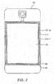
- FIG. 2is a view illustrating another example of an exterior configuration of an apparatus 101, and illustrates a rear surface of the apparatus 101 in a case in which the apparatus 101 is a mobile device such as a smartphone.
- reference numeral 111denotes a receiving coil formed on a rear surface of the apparatus 101
- reference numerals 121-1 and 121-2denote insulating portions
- reference numeral 131denotes the rear surface of the apparatus 101.
- a portion of the case of the apparatus 101is formed by the receiving coil 111, the insulating portions 121-1 and 121-2, and the rear surface 131.
- the rear surface 131is a casing region that surrounds at least a portion of the apparatus 101.
- the receiving coil 111is formed along an edge of the rear surface 131 of the apparatus 101, thereby allowing the apparatus 101 to receive power wirelessly.
- the receiving coil 111is a single conductive wire formed along the edge of the rear surface 131 of the apparatus 101.
- FIG. 2illustrates a case in which the receiving coil 111 is a single conductive wire formed across almost the entire edge of the rear surface 131 of the apparatus 101, the receiving coil 110 may also be formed across the entire edge and may also only be formed in a portion of the edge.
- the receiving coil 111may be formed to have a large number of turns along the edge of the rear surface 131 of the apparatus 101.
- the receiving coil 111may have a ring shape or a polygonal shape having ends that are separated from each other.
- the insulating portions 121-1 and 121-2are disposed between the receiving coil 111 and the rear surface 131 of the apparatus 101. As a result, the receiving coil 111 and the rear surface 131 of the apparatus 101 made of metal are electrically insulated from each other.
- the insulating portion 121-2may be omitted.
- Ends A2 and B2 of the receiving coil 111are connected to an internal circuit of the apparatus.
- the case of the apparatus 101 including the receiving coil 111, the insulating portions 121-1 and 121-2, and the rear surface 131 of the apparatus 101may be integrally formed by a method such as insert injection molding, or any other suitable method.
- the ends A2 and B2 of the receiving coil 111may be provided with a terminal or a lead wire that is electrically connected to the internal circuit of the apparatus 101.
- FIG. 3is a view illustrating an example of an internal circuit of the apparatus.
- the body of the apparatusincludes a printed circuit board (PCB) including the internal circuit, and in the example in FIG. 3 , the internal circuit of the apparatus includes a capacitor C, a switch portion 140, a near-field communication (NFC) module 150, and a wireless charging module 160.
- PCBprinted circuit board
- NFCnear-field communication
- Ldenotes a receiving coil, for example, the receiving coil 110 of FIG. 1 or the receiving coil 111 of FIG. 2 .
- the receiving coil Lreceives power wirelessly from an external power source.
- the receiving coil Lmay also wirelessly receive a data signal in addition to the power.
- the receiving coil L and the capacitor Cform a resonance tank.
- the switch portion 140includes switches S1 and S2, and transfers the power wirelessly received by the receiving coil L to the wireless charging module 160, or transfers the data signal received by the receiving coil L to the NFC module 150.
- the switches S1 and S2 of the switch portion 140may be controlled in response to an input from a user, and may also be controlled according to an amplitude of the signal received by the receiving coil L.
- the signal received by the receiving coil Lmay be determined to be the power that is wirelessly received, and the switches S1 and S2 may be controlled to connect the switch S1 to a terminal b1 and connect the switch S2 to a terminal b2 to connect the receiving coil L and the capacitor C to the wireless charging module 160.
- the signal received by the receiving coil Lmay be determined to be the data signal, and the switches S1 and S2 may be controlled to connect the switch S1 to a terminal a1 and connect the switch S2 to a terminal a2 to connect the receiving coil L and the capacitor C to the NFC module 150.
- the NFC module 150enables the apparatus to transmit and receive data to and from other external apparatuses.
- the wireless charging module 160may include a rectifier, a regulator, and other charging components, and may transfer the power that is wirelessly received to a battery (not illustrated) or other energy storage device of the apparatus.
- FIG. 3illustrates a case in which the switch portion 140 includes two switches S1 and S2, the switch S2 may be omitted in a case in which a terminal a2 and a terminal b2 are connected to a common ground.
- FIGS. 4 through 7are views illustrating examples of configurations in which an apparatus wirelessly receives power from a wireless power transmitter 200.
- FIG. 4illustrates a plan view of an apparatus in a case in which the apparatus has the configuration of FIG. 1 or FIG. 2
- FIG. 5illustrates a cross-sectional view of an apparatus in the case in which the apparatus has the configuration of FIG. 1
- FIGS. 6 and 7illustrate cross-sectional views of an apparatus in a case in which the apparatus has the configuration of FIG. 2 .
- FIGS. 4illustrates a plan view of an apparatus in a case in which the apparatus has the configuration of FIG. 1 or FIG. 2
- FIG. 5illustrates a cross-sectional view of an apparatus in the case in which the apparatus has the configuration of FIG. 1
- FIGS. 6 and 7illustrate cross-sectional views of an apparatus in a case in which the apparatus has the configuration of FIG. 2 .
- FIGS. 4illustrates a plan view of an apparatus in a case in which the apparatus has the configuration
- reference numeral 210denotes a transmitting coil of the wireless power transmitter 200
- reference numeral 220denotes a power source portion of the wireless power transmitter 200
- reference numeral 230denotes a ferrite sheet of the wireless power transmitter 200
- reference numeral 240denotes a case of the wireless power transmitter 200.
- the transmitting coil 210 of the wireless power transmitter 200is formed to surround the receiving coil 110 of the apparatus 100.
- the receiving coil 110 of the apparatus 100is disposed within the transmitting coil 210 of the wireless power transmitter 200.
- FIG. 4illustrates a case in which the transmitting coil 210 has a single winding
- the transmitting coil 210may have a two or more windings.
- Table 1illustrates simulation results for self-inductances of the receiving coil 110 ( FIGS. 1 and 4 ), mutual inductances between the receiving coil 110 and the transmitting coil 210 ( FIG. 4 ), and coupling coefficients between the receiving coil 110 and the transmitting coil 210 according to distances between the ends A1 and B1 ( FIG. 1 ) of the receiving coil 110 in the apparatus 100 having an edge length of 384 mm.
- the edge lengthis a length measured along the entire edge of the apparatus 100.
- the self-inductance, the mutual inductance, and the coupling coefficientbarely change up to the distance between the ends A1 and B1 of the receiving coil 110 of 20 mm, which is about 5% of the edge length of 384 mm of the apparatus, as compared to a case in which the distance between the ends A1 and B1 of the receiving coil 110 is 0 mm, that is, a case in which the receiving coil entirely surrounds the edge when viewed from above.
- the receiving coilis formed along 95% or more of the edge, a sufficiently high value of wireless charging efficiency may be achieved.
- FIG. 5illustrates an example of a configuration in which the apparatus 100 wirelessly receives power from the wireless power transmitter 200, and illustrates a cross-sectional view of a case in which the apparatus 100 having the configuration of FIG. 1 is disposed on the wireless power transmitter 200 to wirelessly receive power.
- the apparatus 100includes the rear surface 130, the insulating portions 120-1 and 120-2, the receiving coil 110, a front surface 133, and a body 170.
- the receiving coil 110 of the apparatus 100is disposed outside the rear surface 130 of the apparatus 100 made of metal.
- the insulating portion 120-1is disposed between the receiving coil 110 and the rear surface 130 of the apparatus 100.
- the insulating portion 120-2is disposed between the receiving coil 110 and the front surface 133 of the apparatus 100.
- the front surface 133 of the apparatus 100is not made of metal, there is no need to insulate the front surface 133 of the apparatus 100 and the receiving coil 110 from each other, so the insulating portion 120-2 may be omitted.
- the front surface 133 of the apparatus 100which is provided to protect a display device, is made of a transparent material.
- the front surface 133 of the apparatus 100may also be extended to portions of the side surface of the apparatus 100.
- the capacitor C, the switch portion 140, the NFC module 150, and the wireless charging module 160 illustrated in FIG. 3are disposed in the body 170 of the apparatus 100.
- the transmitting coil 210 of the wireless power transmitter 200is disposed outside the receiving coil 110 of the apparatus 100.
- FIGS. 6 and 7illustrate examples of a configuration in which the apparatus wirelessly receives power from the wireless power transmitter, and illustrate cross-sectional views of the apparatus in a case in which the apparatus having the configuration of FIG. 2 is disposed on the wireless power transmitter to wirelessly receive power.
- an apparatus 101includes include a rear surface 131, a receiving coil 111, insulating portions 121-1 and 121-2, an edge 135, a front surface 134, and a body 171.
- an apparatus 102includes a rear surface 131-1, a receiving coil 112, an insulating portion 122, an edge 135-1, a front surface 134-1, and a body 171-1.
- the receiving coil 111 or 112is disposed outside the rear surface 131 or 131-1 of the apparatus 101 or 102.
- the insulating portion 121-1 or 122is disposed between the receiving coil 111 or 112 and the rear surface 131 or 131-1 of the apparatus 101 or 102.
- the insulating portion 121-2is disposed between the edge 135 of the apparatus 101 and the receiving coil 111.
- the insulating portion 121-2 in FIG. 6not disposed between the edge 135-1 of the apparatus 102 and the receiving coil 112.
- the front surface 134 or 134-1 of the apparatus 101 or 102which is to protect a display device, is made of a transparent material.
- the front surface 134 or 134-1 of the apparatus 101 or 102may also be extended to portions of the side surface of the apparatus 101 or 102.
- the capacitor C, the switch portion 140, the NFC module 150, and the wireless charging module 160 illustrated in FIG. 3are disposed in the body 171 or 171-1 of the apparatus 101 or 102.
- the transmitting coil 210 of the wireless power transmitter 200is disposed outside the receiving coil 111 or 112 of the apparatus 101 or 102.
- the apparatusis able to wirelessly receive power transmitted by the transmitting coil of the wireless power transmitter.
- the apparatusis able to wirelessly receive power or transmit and receive data without affecting a design of the apparatus even in a case in which the metal case is used.
Landscapes
- Engineering & Computer Science (AREA)
- Computer Networks & Wireless Communication (AREA)
- Power Engineering (AREA)
- Signal Processing (AREA)
- Charge And Discharge Circuits For Batteries Or The Like (AREA)
- Near-Field Transmission Systems (AREA)
Description
- This application relates to a case including a coil for receiving power wirelessly or performing near-field communication, and an apparatus including the same.
- In accordance with the development of wireless technology, various wireless functions ranging from the transmission of data to the transmission of power have been implemented. In accordance with the trend for mobile devices such as cellular phones, tablets, and other mobile devices to be protected from water and dust, wireless power reception technology is increasingly being demanded in mobile devices. In addition, in order to perform a function such as electronic payment approval or other function requiring data communication using a mobile device, near-field communication functionality is also being demanded in mobile devices.
US 2014/0159502 A1 discloses wirelessly transmitting power to a smartphone. A coil for wirelessly receiving power is encapsulated in a jacket-shaped cover part for covering the rear and lateral sides of the smartphone. The cover part is made of a non-magnetic material in order to suppress turbulence or loss of magnetic flux. Further, the cover part is made of an electrically non-conductive material in order to suppress loss of electric power due to eddy current generation during power transmission. For example, the cover part may be made by insert-molding thermoplastic polycarbonate resin.US 2012/0329535 A1 discloses a metallic jacket for covering an outside of a mobile phone.- Mobile devices such as cellular phones, tablets, and other mobile devices have increasingly been provided with metal cases due to a customer demand. However, when a rear surface of the mobile device is formed by a metal case, even in the case that a coil for wirelessly receiving power or performing near-field communication is disposed in the metal case, the power may not be wirelessly received or data may not be transmitted and received due to the metal case.
TW M 475 107 U - It is an object of the invention to provide an improved case for an electronic device which allows wirelessly receiving power or performing wireless communication, and an apparatus including such a case.
- The invention is set out in the independent claims whereas preferred embodiments are outlined in the dependent claims.
FIG. 1 is a view illustrating an example of an exterior configuration of an apparatus.FIG. 2 is a view illustrating another example of an exterior configuration of an apparatus.FIG. 3 is a view illustrating an example of an internal circuit of the apparatus.FIGS. 4 through 7 are views illustrating examples of configurations in which the apparatus receives power wirelessly from a wireless power transmitter.- Throughout the drawings and the detailed description, the same reference numerals refer to the same elements. The drawings may not be to scale, and the relative size, proportions, and depiction of elements in the drawings may be exaggerated for clarity,
comprehensive understanding of the methods, apparatuses, and/or systems described herein. However, various changes, modifications, and equivalents of the methods, apparatuses, and/or systems described herein will be apparent to one of ordinary skill in the art. The sequences of operations described herein are merely examples, and are not limited to those set forth herein, but may be changed as will be apparent to one of ordinary skill in the art, with the exception of operations necessarily occurring in a certain order. Also, descriptions of functions and constructions that are well known to one of ordinary skill in the art may be omitted for increased clarity and conciseness. - The features described herein may be embodied in different forms, and are not to be construed as being limited to the examples described herein. Rather, the examples described herein have been provided so that this disclosure will be thorough and complete, and will convey the full scope of the disclosure to one of ordinary skill in the art.
- The invention is defined by the appended claims. In the following, embodiments not falling within the scope of the claims should be understood as examples useful to understand the invention.
FIG. 1 is a view illustrating an example of an exterior configuration of anapparatus 100, and illustrates a perspective view of a rear surface of theapparatus 100 in a case in which theapparatus 100 is a mobile device such as a smartphone. InFIG. 1 ,reference numeral 110 denotes a receiving coil formed on a side surface of theapparatus 100, reference numerals 120-1 and 120-2 denote insulating portions, andreference numeral 130 denotes a rear surface of the apparatus. A portion of the case of theapparatus 100 is formed by thereceiving coil 110, the insulating portions 120-1 and 120-2, and therear surface 130. Therear surface 130 is a casing region that surrounds at least a portion of theapparatus 100.- In a case in which the
rear surface 130 of theapparatus 100 is made of metal, thereceiving coil 110 is formed along an edge of theapparatus 100, thereby allowing theapparatus 100 to receive power wirelessly. In the example inFIG. 1 , thereceiving coil 110 is a single conductive wire formed along the edge of theapparatus 100. AlthoughFIG. 1 illustrates a case in which thereceiving coil 110 is a single conductive wire formed across almost the entire edge of theapparatus 100, thereceiving coil 110 may also be formed across the entire edge and may also be formed only in a portion of the edge. In addition, thereceiving coil 110 may be formed to have a large number of turns along the edge of theapparatus 100. Thereceiving coil 110 may have a ring shape or a polygonal shape having ends that are separated from each other. - The insulating portion 120-1 is disposed between the
receiving coil 110 and therear surface 130 of theapparatus 100. Thus, the receivingcoil 110 and therear surface 130 of theapparatus 100 made of metal are electrically insulated from each other. - The insulating portion 120-2 is also disposed between the
receiving coil 110 and a front surface of theapparatus 100. However, in a case in which a material of the front surface of theapparatus 100 is not made of metal, the insulating portion 120-2 may be omitted. - Alternatively, the edge of the
apparatus 100 may include the insulating portions 120-1 and 120-2 and thereceiving coil 110. In this case, other portions of the edge of theapparatus 100, that is, a portion thereof between the insulating portion 120-1 and therear surface 130 of theapparatus 100 and a portion thereof between the insulating portion 120-2 and the front surface of theapparatus 100 may be made of metal. - Ends A1 and B1 of the
receiving coil 110 are connected to an internal circuit of the apparatus. - Although
FIG. 1 illustrates a case in which thereceiving coil 110 is formed separately on the edge of theapparatus 100, the edge of theapparatus 100 may be formed of metal and may also be used as a receiving coil for receiving power wirelessly. In detail, thereceiving coil 110 may be formed using a method of forming the edge of theapparatus 100 using metal and then forming the insulating portions 120-1 and 120-2. - The case of the
apparatus 100 including the receivingcoil 110, the insulating portions 120-1 and 120-2, and therear surface 130 of theapparatus 100 may be integrally formed by a method such as insert injection molding, or any other suitable method. In this case, the ends A1 and 81 of thereceiving coil 110 may be provided with a terminal or a lead wire that is electrically connected to the internal circuit of theapparatus 100. FIG. 2 is a view illustrating another example of an exterior configuration of anapparatus 101, and illustrates a rear surface of theapparatus 101 in a case in which theapparatus 101 is a mobile device such as a smartphone. InFIG. 2 ,reference numeral 111 denotes a receiving coil formed on a rear surface of theapparatus 101, reference numerals 121-1 and 121-2 denote insulating portions, andreference numeral 131 denotes the rear surface of theapparatus 101. A portion of the case of theapparatus 101 is formed by thereceiving coil 111, the insulating portions 121-1 and 121-2, and therear surface 131. Therear surface 131 is a casing region that surrounds at least a portion of theapparatus 101.- In the case of the
apparatus 101, when therear surface 131 of theapparatus 101 is made of metal, thereceiving coil 111 is formed along an edge of therear surface 131 of theapparatus 101, thereby allowing theapparatus 101 to receive power wirelessly. In the example inFIG. 2 , thereceiving coil 111 is a single conductive wire formed along the edge of therear surface 131 of theapparatus 101. AlthoughFIG. 2 illustrates a case in which thereceiving coil 111 is a single conductive wire formed across almost the entire edge of therear surface 131 of theapparatus 101, thereceiving coil 110 may also be formed across the entire edge and may also only be formed in a portion of the edge. In addition, the receivingcoil 111 may be formed to have a large number of turns along the edge of therear surface 131 of theapparatus 101. The receivingcoil 111 may have a ring shape or a polygonal shape having ends that are separated from each other. - The insulating portions 121-1 and 121-2 are disposed between the receiving
coil 111 and therear surface 131 of theapparatus 101. As a result, the receivingcoil 111 and therear surface 131 of theapparatus 101 made of metal are electrically insulated from each other. - In a case in which portions of the
apparatus 101 except for therear surface 131 formed inwardly of the receivingcoil 111, and in a case in which sides of the apparatus are formed of a non-metallic material, the insulating portion 121-2 may be omitted. - Ends A2 and B2 of the receiving
coil 111 are connected to an internal circuit of the apparatus. - The case of the
apparatus 101 including the receivingcoil 111, the insulating portions 121-1 and 121-2, and therear surface 131 of theapparatus 101 may be integrally formed by a method such as insert injection molding, or any other suitable method. In this case, the ends A2 and B2 of the receivingcoil 111 may be provided with a terminal or a lead wire that is electrically connected to the internal circuit of theapparatus 101. FIG. 3 is a view illustrating an example of an internal circuit of the apparatus. The body of the apparatus includes a printed circuit board (PCB) including the internal circuit, and in the example inFIG. 3 , the internal circuit of the apparatus includes a capacitor C, aswitch portion 140, a near-field communication (NFC)module 150, and awireless charging module 160. InFIG. 3 , reference numeral L denotes a receiving coil, for example, the receivingcoil 110 ofFIG. 1 or the receivingcoil 111 ofFIG. 2 .- The receiving coil L receives power wirelessly from an external power source. The receiving coil L may also wirelessly receive a data signal in addition to the power. The receiving coil L and the capacitor C form a resonance tank.
- The
switch portion 140 includes switches S1 and S2, and transfers the power wirelessly received by the receiving coil L to thewireless charging module 160, or transfers the data signal received by the receiving coil L to theNFC module 150. The switches S1 and S2 of theswitch portion 140 may be controlled in response to an input from a user, and may also be controlled according to an amplitude of the signal received by the receiving coil L. For example, when the amplitude of the signal received by the receiving coil L is equal to or higher than a reference amplitude, the signal received by the receiving coil L may be determined to be the power that is wirelessly received, and the switches S1 and S2 may be controlled to connect the switch S1 to a terminal b1 and connect the switch S2 to a terminal b2 to connect the receiving coil L and the capacitor C to thewireless charging module 160. Alternatively, when the amplitude of the signal received by the receiving coil L is lower than the reference amplitude, the signal received by the receiving coil L may be determined to be the data signal, and the switches S1 and S2 may be controlled to connect the switch S1 to a terminal a1 and connect the switch S2 to a terminal a2 to connect the receiving coil L and the capacitor C to theNFC module 150. - The
NFC module 150 enables the apparatus to transmit and receive data to and from other external apparatuses. - The
wireless charging module 160 may include a rectifier, a regulator, and other charging components, and may transfer the power that is wirelessly received to a battery (not illustrated) or other energy storage device of the apparatus. - Although
FIG. 3 illustrates a case in which theswitch portion 140 includes two switches S1 and S2, the switch S2 may be omitted in a case in which a terminal a2 and a terminal b2 are connected to a common ground. FIGS. 4 through 7 are views illustrating examples of configurations in which an apparatus wirelessly receives power from awireless power transmitter 200. In detail,FIG. 4 illustrates a plan view of an apparatus in a case in which the apparatus has the configuration ofFIG. 1 orFIG. 2 ,FIG. 5 illustrates a cross-sectional view of an apparatus in the case in which the apparatus has the configuration ofFIG. 1 , andFIGS. 6 and 7 illustrate cross-sectional views of an apparatus in a case in which the apparatus has the configuration ofFIG. 2 . InFIGS. 4 through 7 ,reference numeral 210 denotes a transmitting coil of thewireless power transmitter 200,reference numeral 220 denotes a power source portion of thewireless power transmitter 200,reference numeral 230 denotes a ferrite sheet of thewireless power transmitter 200, andreference numeral 240 denotes a case of thewireless power transmitter 200.- As illustrated in
FIG. 4 , in order to wirelessly transmit power to theapparatus 100, the transmittingcoil 210 of thewireless power transmitter 200 is formed to surround the receivingcoil 110 of theapparatus 100. In detail, in order to wirelessly transmit power, the receivingcoil 110 of theapparatus 100 is disposed within the transmittingcoil 210 of thewireless power transmitter 200. - Although
FIG. 4 illustrates a case in which the transmittingcoil 210 has a single winding, the transmittingcoil 210 may have a two or more windings. - Table 1 illustrates simulation results for self-inductances of the receiving coil 110 (
FIGS. 1 and4 ), mutual inductances between the receivingcoil 110 and the transmitting coil 210 (FIG. 4 ), and coupling coefficients between the receivingcoil 110 and the transmittingcoil 210 according to distances between the ends A1 and B1 (FIG. 1 ) of the receivingcoil 110 in theapparatus 100 having an edge length of 384 mm. The edge length is a length measured along the entire edge of theapparatus 100.Table 1 Classification Distances Between Ends A1 and A2 of Receiving Coil 0 mm 5 mm 10 mm 20 mm 30 mm Self-Inductance 0.293 0.292 0.289 0.299 0.255 Mutual Inductance 0.166 0.166 0.165 0.168 0.143 Coupling Coefficient 0.473 0.473 0.474 0.472 0.440 - It can be seen from Table 1 that the self-inductance, the mutual inductance, and the coupling coefficient barely change up to the distance between the ends A1 and B1 of the receiving
coil 110 of 20 mm, which is about 5% of the edge length of 384 mm of the apparatus, as compared to a case in which the distance between the ends A1 and B1 of the receivingcoil 110 is 0 mm, that is, a case in which the receiving coil entirely surrounds the edge when viewed from above. In other words, when the receiving coil is formed along 95% or more of the edge, a sufficiently high value of wireless charging efficiency may be achieved. FIG. 5 illustrates an example of a configuration in which theapparatus 100 wirelessly receives power from thewireless power transmitter 200, and illustrates a cross-sectional view of a case in which theapparatus 100 having the configuration ofFIG. 1 is disposed on thewireless power transmitter 200 to wirelessly receive power. Theapparatus 100 includes therear surface 130, the insulating portions 120-1 and 120-2, the receivingcoil 110, afront surface 133, and abody 170.- When viewed from above, the receiving
coil 110 of theapparatus 100 is disposed outside therear surface 130 of theapparatus 100 made of metal. The insulating portion 120-1 is disposed between the receivingcoil 110 and therear surface 130 of theapparatus 100. In addition, the insulating portion 120-2 is disposed between the receivingcoil 110 and thefront surface 133 of theapparatus 100. However, in a case in which thefront surface 133 of theapparatus 100 is not made of metal, there is no need to insulate thefront surface 133 of theapparatus 100 and the receivingcoil 110 from each other, so the insulating portion 120-2 may be omitted. - The
front surface 133 of theapparatus 100, which is provided to protect a display device, is made of a transparent material. Thefront surface 133 of theapparatus 100 may also be extended to portions of the side surface of theapparatus 100. - The capacitor C, the
switch portion 140, theNFC module 150, and thewireless charging module 160 illustrated inFIG. 3 are disposed in thebody 170 of theapparatus 100. - The transmitting
coil 210 of thewireless power transmitter 200 is disposed outside the receivingcoil 110 of theapparatus 100. FIGS. 6 and 7 illustrate examples of a configuration in which the apparatus wirelessly receives power from the wireless power transmitter, and illustrate cross-sectional views of the apparatus in a case in which the apparatus having the configuration ofFIG. 2 is disposed on the wireless power transmitter to wirelessly receive power. Referring toFIG. 6 , anapparatus 101 includes include arear surface 131, a receivingcoil 111, insulating portions 121-1 and 121-2, anedge 135, afront surface 134, and abody 171. Referring toFIG. 7 , anapparatus 102 includes a rear surface 131-1, a receivingcoil 112, an insulatingportion 122, an edge 135-1, a front surface 134-1, and a body 171-1.- The receiving
coil rear surface 131 or 131-1 of theapparatus coil rear surface 131 or 131-1 of theapparatus - As illustrated in
FIG. 6 , for example, when theedge 135 of theapparatus 101 is made of metal, the insulating portion 121-2 is disposed between theedge 135 of theapparatus 101 and the receivingcoil 111. As illustrated inFIG. 7 , in a case in which the edge 135-1 of theapparatus 102 is made of a non-metallic material, the insulating portion 121-2 inFIG. 6 not disposed between the edge 135-1 of theapparatus 102 and the receivingcoil 112. - The
front surface 134 or 134-1 of theapparatus front surface 134 or 134-1 of theapparatus apparatus - The capacitor C, the
switch portion 140, theNFC module 150, and thewireless charging module 160 illustrated inFIG. 3 are disposed in thebody 171 or 171-1 of theapparatus - The transmitting
coil 210 of thewireless power transmitter 200 is disposed outside the receivingcoil apparatus - In the examples described above, even in the case that the rear surface of the apparatus that is in contact with the wireless power transmitter is made of metal, the apparatus is able to wirelessly receive power transmitted by the transmitting coil of the wireless power transmitter.
- In the examples described above, the apparatus is able to wirelessly receive power or transmit and receive data without affecting a design of the apparatus even in a case in which the metal case is used.
- While this disclosure includes specific examples, it will be apparent to one of ordinary skill in the art that various changes in form and details may be made in these examples without departing from the scope of the claims. The examples described herein are to be considered in a descriptive sense only, and not for purposes of limitation. Descriptions of features or aspects in each example are to be considered as being applicable to similar features or aspects in other examples. Suitable results may be achieved if the described techniques are performed in a different order, and/or if components in a described system, architecture, device, or circuit are combined in a different manner, and/or replaced or supplemented by other components or their equivalents. Therefore, the scope of the disclosure is defined not by the detailed description, but by the claims and all variations within the scope of the claims are to be construed as being included in the disclosure.
Claims (10)
- A case comprising:a casing region (130, 131, 131-1) made of metal and configured to cover at least a portion of an apparatus;a coil (110, 111, 112) electrically insulated from the casing region and having a ring shape or a polygonal shape having ends separated from each other, the coil being configured to be disposed outside the apparatus; andan insulating portion (120-1, 120-2, 121-1, 121-2, 122) disposed between the casing region (130, 131, 131-1) and the coil (110, 111, 112),characterized in thatthe coil (110, 111, 112) is constituted by a single conductive wire formed across almost the entire edge of the apparatus.
- The case of claim 1, wherein the casing region (130, 131, 131-1) comprises a region corresponding to a rear surface of the apparatus.
- The case of claim 2, wherein the coil (110, 111, 112) is disposed in a position corresponding to an edge of the rear surface of the apparatus.
- The case of claim 1, wherein the coil (110, 111, 112) comprises two or more turns.
- An apparatus comprising:a body (170, 171, 171-1); anda case comprising:a casing region (130, 131, 131-1) made of metal and covering at least a portion of the body;a coil (110, 111, 112) electrically insulated from the casing region and having a ring shape or a polygonal shape having ends separated from each other, the coil being disposed outside the body; andan insulating portion (120-1, 120-2, 121-1, 121-2, 122) disposed between the casing region (130, 131, 131-1) and the coil (110, 111, 112),characterized in thatthe coil (110, 111, 112) is constituted by a single conductive wire formed across almost the entire edge of the apparatus.
- The apparatus of claim 5, wherein the body (170, 171, 171-1) comprises a wireless charging module (160) configured to rectify power wirelessly received through the coil to charge a battery with power.
- The apparatus of claim 5, wherein the body (170, 171, 171-1) comprises a near-field communication, NFC, module (150) configured to transmit and receive data through the coil.
- The apparatus of claim 5, wherein the body (170, 171, 171-1) comprises:a wireless charging module (160) configured to rectify power wirelessly received through the coil to charge a battery with power;a near-field communication, NFC, module (150) configured to transmit and receive data through the coil; anda switch portion (140) configured to selectively connect the coil to the NFC module or the wireless charging module in response to a signal received by the coil.
- The apparatus of claim 5, wherein the coil (110, 111, 112) is disposed along an edge of a rear surface of the body.
- The apparatus of claim 5, wherein:the casing region (130, 131, 131-1) comprises a region corresponding to a rear surface of the apparatus; andthe coil constitutes a portion of the case.
Applications Claiming Priority (2)
| Application Number | Priority Date | Filing Date | Title |
|---|---|---|---|
| KR20140117835 | 2014-09-04 | ||
| KR1020150056927AKR101681412B1 (en) | 2014-09-04 | 2015-04-23 | A case and a apparatus comprising the case |
Publications (2)
| Publication Number | Publication Date |
|---|---|
| EP2992776A1 EP2992776A1 (en) | 2016-03-09 |
| EP2992776B1true EP2992776B1 (en) | 2019-11-06 |
Family
ID=54010959
Family Applications (1)
| Application Number | Title | Priority Date | Filing Date |
|---|---|---|---|
| EP15182620.3AActiveEP2992776B1 (en) | 2014-09-04 | 2015-08-27 | Case and apparatus including the same |
Country Status (3)
| Country | Link |
|---|---|
| US (1) | US20160072337A1 (en) |
| EP (1) | EP2992776B1 (en) |
| CN (1) | CN105405578B (en) |
Families Citing this family (12)
| Publication number | Priority date | Publication date | Assignee | Title |
|---|---|---|---|---|
| USD795184S1 (en)* | 2015-08-12 | 2017-08-22 | Samsung Electronics Co., Ltd. | Wireless charger for electronic device |
| TW201725828A (en)* | 2015-08-13 | 2017-07-16 | 維電股份有限公司 | Wireless power enabled enclosures for mobile devices |
| US10361588B2 (en)* | 2015-12-07 | 2019-07-23 | Qualcomm Incorporated | Coupled resonator in a metal back cover |
| EP3229335B1 (en) | 2016-04-06 | 2019-02-06 | Vestel Elektronik Sanayi ve Ticaret A.S. | Cover, mobile device and energy management method |
| WO2018028486A1 (en)* | 2016-08-08 | 2018-02-15 | Guangdong Oppo Mobile Telecommunications Corp., Ltd. | Housing, method for manufacturing housing, and mobile terminal having housing |
| US10622820B2 (en) | 2016-09-23 | 2020-04-14 | Apple Inc. | Bobbin structure and transmitter coil for wireless charging mats |
| KR20180044562A (en)* | 2016-10-24 | 2018-05-03 | 삼성전기주식회사 | Wireless power receiving device |
| WO2018120921A1 (en) | 2016-12-29 | 2018-07-05 | Guangdong Oppo Mobile Telecommunications Corp., Ltd. | Mobile terminal |
| KR102119591B1 (en) | 2017-09-14 | 2020-06-05 | 주식회사 아모센스 | wireless power transmission device |
| CN107994317B (en)* | 2017-11-21 | 2020-05-08 | Oppo广东移动通信有限公司 | A casing, an antenna device and a mobile terminal |
| US20190215984A1 (en) | 2018-01-09 | 2019-07-11 | Aptiv Technologies Limited | Wireless device charger with cooling device |
| US20230187973A1 (en)* | 2021-12-14 | 2023-06-15 | Datalogic Ip Tech S.R.L. | Resonant wireless power transfer charging pad for unplanar devices |
Citations (1)
| Publication number | Priority date | Publication date | Assignee | Title |
|---|---|---|---|---|
| TWM475107U (en)* | 2013-09-17 | 2014-03-21 | Jess Link Products Co Ltd | Back cover with wireless charging function |
Family Cites Families (112)
| Publication number | Priority date | Publication date | Assignee | Title |
|---|---|---|---|---|
| US4374354A (en)* | 1981-06-23 | 1983-02-15 | Teledyne Industries, Inc. | Rechargeable electric portable appliance |
| EP0977215A3 (en)* | 1996-08-09 | 2000-12-06 | SUMITOMO WIRING SYSTEMS, Ltd. | Charging connector for electric vehicle |
| US5966799A (en)* | 1997-04-01 | 1999-10-19 | Motorola, Inc. | Method of molding free-floating insert |
| US7478108B2 (en)* | 1999-12-06 | 2009-01-13 | Micro Strain, Inc. | Data collection using sensing units and separate control units with all power derived from the control units |
| US6810275B2 (en)* | 2000-12-20 | 2004-10-26 | Motorola, Inc. | Hand-held communication device with vertically oriented antenna |
| JP3905418B2 (en)* | 2001-05-18 | 2007-04-18 | セイコーインスツル株式会社 | Power supply device and electronic device |
| US6894456B2 (en)* | 2001-11-07 | 2005-05-17 | Quallion Llc | Implantable medical power module |
| US6839029B2 (en)* | 2002-03-15 | 2005-01-04 | Etenna Corporation | Method of mechanically tuning antennas for low-cost volume production |
| US6822609B2 (en)* | 2002-03-15 | 2004-11-23 | Etenna Corporation | Method of manufacturing antennas using micro-insert-molding techniques |
| KR20030090477A (en)* | 2002-05-21 | 2003-11-28 | 이환덕 | Insert molding of one body type and making method thereof |
| JP4539038B2 (en)* | 2003-06-30 | 2010-09-08 | ソニー株式会社 | Data communication device |
| DE102004017832B3 (en)* | 2004-04-13 | 2005-10-20 | Siemens Audiologische Technik | hearing Aid |
| DE102004062178B4 (en)* | 2004-12-21 | 2007-10-11 | Bury Sp.Z.O.O | Telephone system with a holding device for receiving a mobile phone |
| WO2006106982A1 (en)* | 2005-04-01 | 2006-10-12 | Nissha Printing Co., Ltd. | Transparent antenna for display, light transmissive member for display, having antenna, and part for housing, having antenna |
| JP4603409B2 (en)* | 2005-04-22 | 2010-12-22 | 出光興産株式会社 | Magnetic levitation railway ground coil device and manufacturing method thereof |
| US8169185B2 (en)* | 2006-01-31 | 2012-05-01 | Mojo Mobility, Inc. | System and method for inductive charging of portable devices |
| JP2008040904A (en)* | 2006-08-08 | 2008-02-21 | Hitachi Ltd | RFID tag and reading method thereof |
| JP5300187B2 (en)* | 2006-09-07 | 2013-09-25 | 三洋電機株式会社 | Pack battery charged by magnetic induction |
| US7699989B2 (en)* | 2006-10-17 | 2010-04-20 | Millipore Corporation | Powered cartridges and other devices within housings |
| FR2914800B1 (en)* | 2007-04-04 | 2010-09-17 | Jacek Kowalski | NFC MODULE, IN PARTICULAR FOR MOBILE TELEPHONE |
| JP4896820B2 (en)* | 2007-05-29 | 2012-03-14 | ソニー・エリクソン・モバイルコミュニケーションズ株式会社 | Coil module device |
| US8626297B2 (en)* | 2007-09-20 | 2014-01-07 | Boston Scientific Neuromodulation Corporation | Apparatus and methods for charging an implanted medical device power source |
| WO2009042214A1 (en)* | 2007-09-26 | 2009-04-02 | Governing Dynamics, Llc | Self-charging electric vehicles and aircraft, and wireless energy distribution system |
| US20090153412A1 (en)* | 2007-12-18 | 2009-06-18 | Bing Chiang | Antenna slot windows for electronic device |
| US8633616B2 (en)* | 2007-12-21 | 2014-01-21 | Cynetic Designs Ltd. | Modular pocket with inductive power and data |
| KR100976161B1 (en)* | 2008-02-20 | 2010-08-16 | 정춘길 | Contactless charging system and its charging control method |
| JP4540723B2 (en)* | 2008-04-24 | 2010-09-08 | 三洋電機株式会社 | Pack battery |
| JP4519180B2 (en)* | 2008-04-24 | 2010-08-04 | 三洋電機株式会社 | Charging stand, portable device and charging stand, and battery pack and charging stand |
| KR101501921B1 (en)* | 2008-05-06 | 2015-03-13 | 삼성전자주식회사 | Patent application title: PORTABLE TERMINAL WITH METAL CASE |
| US20110050164A1 (en)* | 2008-05-07 | 2011-03-03 | Afshin Partovi | System and methods for inductive charging, and improvements and uses thereof |
| CN101578019A (en)* | 2008-05-09 | 2009-11-11 | 富准精密工业(深圳)有限公司 | Electronic device shell and manufacture method thereof |
| JP2010028969A (en)* | 2008-07-17 | 2010-02-04 | Sanyo Electric Co Ltd | Charger |
| US8581542B2 (en)* | 2008-09-08 | 2013-11-12 | Qualcomm Incorporated | Receive antenna arrangement for wireless power |
| WO2013102901A1 (en)* | 2012-01-05 | 2013-07-11 | Powermat Technologies Ltd | Integrated inductive power receiver and near field communicator |
| US8810194B2 (en)* | 2008-11-20 | 2014-08-19 | Qualcomm Incorporated | Retrofitting wireless power and near-field communication in electronic devices |
| CN101771283B (en)* | 2008-12-29 | 2012-10-10 | 鸿富锦精密工业(深圳)有限公司 | Charging system |
| US9240824B2 (en)* | 2009-02-13 | 2016-01-19 | Qualcomm Incorporated | Wireless power and wireless communication for electronic devices |
| US8325094B2 (en)* | 2009-06-17 | 2012-12-04 | Apple Inc. | Dielectric window antennas for electronic devices |
| US8896487B2 (en)* | 2009-07-09 | 2014-11-25 | Apple Inc. | Cavity antennas for electronic devices |
| EP2454119A2 (en)* | 2009-07-15 | 2012-05-23 | Conductix-Wampfler AG | System for inductively charging vehicles, comprising an electronic positioning aid |
| US8269677B2 (en)* | 2009-09-03 | 2012-09-18 | Apple Inc. | Dual-band cavity-backed antenna for integrated desktop computer |
| US8963782B2 (en)* | 2009-09-03 | 2015-02-24 | Apple Inc. | Cavity-backed antenna for tablet device |
| EP2529469B1 (en)* | 2010-01-27 | 2017-06-14 | Cynetic Designs Ltd | Modular pocket with inductive power and data |
| EP2535906B1 (en)* | 2010-02-05 | 2017-11-01 | Hitachi Metals, Ltd. | Magnetic circuit for a non-contact charging device, power supply device, power receiving device, and non-contact charging device |
| JP5305113B2 (en)* | 2010-05-11 | 2013-10-02 | サムソン エレクトロ−メカニックス カンパニーリミテッド. | Electronic device case in which antenna pattern for low frequency is embedded, manufacturing mold and manufacturing method thereof |
| EP2386401A1 (en)* | 2010-05-11 | 2011-11-16 | Samsung Electro-Mechanics Co., Ltd. | Case of electronic device having antenna pattern embedde therein, and mold therefor and mthod of manufacturing thereof |
| EP2386400A1 (en)* | 2010-05-11 | 2011-11-16 | Samsung Electro-Mechanics Co., Ltd. | Case of electronic device having antenna pattern frame embedded therein, mold therefor and method of manufacturing thereof |
| US20120106103A1 (en)* | 2010-06-23 | 2012-05-03 | Tanios Nohra | Radio frequency energy harvesting enclosure for radio frequency connected devices |
| JP2012049434A (en)* | 2010-08-30 | 2012-03-08 | Sony Corp | Electronic component, feeder device, power receiver, and wireless feeder system |
| US8749438B2 (en)* | 2010-09-29 | 2014-06-10 | Qualcomm Incorporated | Multiband antenna for a mobile device |
| US8983374B2 (en)* | 2010-12-13 | 2015-03-17 | Qualcomm Incorporated | Receiver for near field communication and wireless power functionalities |
| JP2012143091A (en)* | 2011-01-04 | 2012-07-26 | Kimitake Utsunomiya | Remotely and wirelessly driven charger |
| JP5950549B2 (en)* | 2011-03-30 | 2016-07-13 | デクセリアルズ株式会社 | Antenna device, communication device |
| US20120274148A1 (en)* | 2011-04-27 | 2012-11-01 | Samsung Electro-Mechanics Co., Ltd. | Contactless power transmission device and electronic device having the same |
| JP5293907B2 (en)* | 2011-06-13 | 2013-09-18 | 株式会社村田製作所 | Antenna device and communication terminal device |
| JP5342073B2 (en)* | 2011-06-14 | 2013-11-13 | パナソニック株式会社 | Communication device |
| CN202127432U (en)* | 2011-06-22 | 2012-01-25 | 郭琅 | Screw-free metal phone case structure |
| WO2013003527A1 (en)* | 2011-06-28 | 2013-01-03 | Wireless Ev Charge, Llc | Alignment, verification, and optimization of high power wireless charging systems |
| US9059591B2 (en)* | 2011-08-30 | 2015-06-16 | L&P Property Management Company | Docking station for inductively charged portable electronic device |
| WO2013031025A1 (en)* | 2011-09-02 | 2013-03-07 | 富士通株式会社 | Power relay |
| KR20130032545A (en)* | 2011-09-23 | 2013-04-02 | 삼성전자주식회사 | Mobile terminal having an antenna |
| US8676280B2 (en)* | 2011-10-20 | 2014-03-18 | Zalman Tech Co., Ltd. | Antenna case for enhancing transmission and reception of radio waves |
| US9300033B2 (en)* | 2011-10-21 | 2016-03-29 | Futurewei Technologies, Inc. | Wireless communication device with an antenna adjacent to an edge of the device |
| JP2013093429A (en)* | 2011-10-25 | 2013-05-16 | Tdk Corp | Non-contact transmission device |
| US8887619B2 (en)* | 2011-10-28 | 2014-11-18 | Medtronic, Inc. | Removable heat management for recharge coils |
| KR20130081620A (en)* | 2012-01-09 | 2013-07-17 | 주식회사 케이더파워 | The reciving set for the wireless charging system |
| WO2013136330A1 (en)* | 2012-03-16 | 2013-09-19 | Powermat Technologies Ltd. | Inductively chargeable batteries |
| JP5865822B2 (en)* | 2012-04-17 | 2016-02-17 | 日東電工株式会社 | Method for forming magnetic field space |
| WO2014011943A1 (en)* | 2012-07-11 | 2014-01-16 | Wireless Research Development | Performance enhancing electronic steerable case antenna employing direct or wireless coupling |
| WO2014036248A1 (en)* | 2012-09-01 | 2014-03-06 | Mophie, Inc. | Wireless communication accessory for a mobile device |
| KR20140036700A (en)* | 2012-09-18 | 2014-03-26 | 엘지전자 주식회사 | Back cover for a mobile terminal |
| US8950638B2 (en)* | 2012-09-25 | 2015-02-10 | Loopy Cases Llc | Finger loop for portable electronic device case |
| KR20140066415A (en)* | 2012-11-23 | 2014-06-02 | 삼성전기주식회사 | Cordless charging apparatus and electronic device having the same |
| JP6017700B2 (en)* | 2012-11-29 | 2016-11-02 | ノキア テクノロジーズ オーユー | Inductive energy transfer coil structure |
| KR102063644B1 (en)* | 2012-12-14 | 2020-02-11 | 엘지이노텍 주식회사 | Wireless power transmitter |
| WO2014125479A1 (en)* | 2013-02-12 | 2014-08-21 | Sis Resources Ltd. | Inductive charging for an electronic cigarette |
| US9287718B2 (en)* | 2013-03-01 | 2016-03-15 | Nokia Technologies Oy | Method, apparatus, and computer program product for foreign object detection parameter and charging data communication with wireless charging capable battery pack |
| CN206564323U (en)* | 2013-04-08 | 2017-10-17 | 株式会社村田制作所 | Communication terminal |
| US9472339B2 (en)* | 2013-05-01 | 2016-10-18 | Delphi Technologies, Inc. | Wireless power transfer system transducers having interchangeable source resonator and capture resonator |
| US9779870B2 (en)* | 2013-05-20 | 2017-10-03 | Nokia Technologies Oy | Method and apparatus for transferring electromagnetic power |
| KR20160067829A (en)* | 2013-06-26 | 2016-06-14 | 비와이디 컴퍼니 리미티드 | Metal shell and cell phone comprising the same |
| EP3057114B1 (en)* | 2013-08-08 | 2018-09-19 | IHI Corporation | Resonator |
| US20150091496A1 (en)* | 2013-10-01 | 2015-04-02 | Blackberry Limited | Bi-directional communication with a device under charge |
| US20150091508A1 (en)* | 2013-10-01 | 2015-04-02 | Blackberry Limited | Bi-directional communication with a device under charge |
| US9672976B2 (en)* | 2013-10-28 | 2017-06-06 | Nokia Corporation | Multi-mode wireless charging |
| US10147538B2 (en)* | 2013-11-08 | 2018-12-04 | Nokia Technologies Oy | Coil arrangement |
| US9461500B2 (en)* | 2013-11-21 | 2016-10-04 | Htc Corporation | Wireless charging receiving device and wireless charging system using the same |
| KR20160145694A (en)* | 2014-04-16 | 2016-12-20 | 위트리시티 코포레이션 | Wireless energy transfer for mobile device applications |
| US20150311740A1 (en)* | 2014-04-28 | 2015-10-29 | Apple Inc. | Encapsulated inductive charging coil |
| US9496602B2 (en)* | 2014-04-28 | 2016-11-15 | Apple Inc. | Plastic electronic device structures with embedded components |
| US9698632B2 (en)* | 2014-05-09 | 2017-07-04 | Otter Products, Llc | Wireless battery charger and charge-receiving device |
| US10381875B2 (en)* | 2014-07-07 | 2019-08-13 | Qualcomm Incorporated | Wireless power transfer through a metal object |
| KR102242363B1 (en)* | 2014-09-11 | 2021-04-20 | 삼성전자주식회사 | Electronic apparatus and method for grip sensing |
| US20160087480A1 (en)* | 2014-09-23 | 2016-03-24 | Qualcomm Incorporated | Charging Apparatus Including Remote Device Reset |
| US10404089B2 (en)* | 2014-09-29 | 2019-09-03 | Apple Inc. | Inductive charging between electronic devices |
| US9742203B2 (en)* | 2014-10-20 | 2017-08-22 | Qualcomm Incorporated | Distributed resonators for wireless power transfer |
| US20160294225A1 (en)* | 2014-12-15 | 2016-10-06 | PogoTec, Inc. | Wireless power systems and methods suitable for charging wearable electronic devices |
| WO2016109577A1 (en)* | 2014-12-29 | 2016-07-07 | PogoTec, Inc. | Police and security camera system utilizing wireless energy transfer |
| US9806421B1 (en)* | 2015-02-04 | 2017-10-31 | Ethertronics, Inc. | NFC antenna system for metalized devices |
| KR102231232B1 (en)* | 2015-02-27 | 2021-03-23 | 삼성전자주식회사 | Antenna and electronic device having it |
| EP3268657A4 (en)* | 2015-03-03 | 2018-12-26 | Attachit LLC | Magnetic mount system |
| WO2016141349A1 (en)* | 2015-03-04 | 2016-09-09 | PogoTec, Inc. | Wireless power base unit and a system and method for body-worn repeater charging of wearable electronic devices |
| DE102015208846B3 (en)* | 2015-05-13 | 2016-08-11 | Sivantos Pte. Ltd. | hearing Aid |
| US10951052B2 (en)* | 2015-06-05 | 2021-03-16 | Pass & Seymour, Inc. | Wireless charger |
| US10116150B2 (en)* | 2015-09-11 | 2018-10-30 | Samsung Electro-Mechanics Co., Ltd. | Conductive plate and electronic device having the same |
| US9966800B2 (en)* | 2015-10-30 | 2018-05-08 | Lg Innotek Co., Ltd. | Wireless power receiving device |
| KR102506711B1 (en)* | 2015-11-02 | 2023-03-08 | 삼성전자주식회사 | Antenna structure and electronic device comprising thereof |
| KR102358304B1 (en)* | 2015-11-13 | 2022-02-04 | 삼성전자 주식회사 | Electronic device having unibody housing and method for manufacturing the same |
| US10074472B2 (en)* | 2015-12-15 | 2018-09-11 | Taiwan Semiconductor Manufacturing Company, Ltd. | InFO coil on metal plate with slot |
| TWI672873B (en)* | 2016-02-25 | 2019-09-21 | 蘋果公司 | Inductive charging ports for portable computing devices |
| US9955325B2 (en)* | 2016-05-06 | 2018-04-24 | Qualcomm Incorporated | Personal medical device interference mitigation |
| KR102329769B1 (en)* | 2017-04-18 | 2021-11-23 | 삼성전자주식회사 | An electronic device comprising an antenna using housing of the electronic device |
- 2015
- 2015-08-27EPEP15182620.3Apatent/EP2992776B1/enactiveActive
- 2015-08-27USUS14/837,635patent/US20160072337A1/ennot_activeAbandoned
- 2015-09-02CNCN201510556398.1Apatent/CN105405578B/enactiveActive
Patent Citations (2)
| Publication number | Priority date | Publication date | Assignee | Title |
|---|---|---|---|---|
| TWM475107U (en)* | 2013-09-17 | 2014-03-21 | Jess Link Products Co Ltd | Back cover with wireless charging function |
| US20150077047A1 (en)* | 2013-09-17 | 2015-03-19 | Jess-Link Products Co., Ltd. | Rear case for wireless charging application |
Also Published As
| Publication number | Publication date |
|---|---|
| CN105405578B (en) | 2018-08-28 |
| EP2992776A1 (en) | 2016-03-09 |
| CN105405578A (en) | 2016-03-16 |
| US20160072337A1 (en) | 2016-03-10 |
Similar Documents
| Publication | Publication Date | Title |
|---|---|---|
| EP2992776B1 (en) | Case and apparatus including the same | |
| US20230208196A1 (en) | Mobile terminal and chargeable communication module | |
| US10326488B2 (en) | Electronic device case with inductive coupling features | |
| KR101653070B1 (en) | Power relay | |
| KR102017621B1 (en) | Coil substrate for cordless charging and electric device using the same | |
| US9461500B2 (en) | Wireless charging receiving device and wireless charging system using the same | |
| KR101890326B1 (en) | Wireless power transfer module and portable auxiliary battery including the same | |
| US20180269716A1 (en) | Transmitter For Wireless Charger | |
| EP3012911A2 (en) | Receiving antenna and wireless power receiving apparatus comprising same | |
| CN103748765A (en) | communication device | |
| EP3633823B1 (en) | Terminal wireless charging receiving device and transmitting device, and wireless charging system | |
| KR20170071498A (en) | A segmented conductive back cover for wireless power transfer | |
| TW201401708A (en) | Antenna sheet for contactless charging device and charging device using said sheet | |
| KR20150131925A (en) | Portable electronic device capable of NFC communication | |
| EP2926433A1 (en) | An inductive energy transfer coil structure | |
| US8855354B2 (en) | Electroacoustic transducer with wireless charging coil | |
| US20150115724A1 (en) | Wireless power receiver and electronic device having the same | |
| KR20160073303A (en) | Wireless charger and wireless power receiver | |
| EP2940792A1 (en) | Case apparatus | |
| KR101765487B1 (en) | Installation method for attenna apparatus with ntc attenna annd wireless charging coil | |
| US20170170689A1 (en) | Wireless charging of metal framed electronic devices | |
| US20180269720A1 (en) | Power transmission device | |
| KR101649258B1 (en) | Flexible printed circuit board for wireless communications | |
| KR102527072B1 (en) | wireless power transfer module embeded in back cover and a portable electronic device having the same | |
| KR101681412B1 (en) | A case and a apparatus comprising the case |
Legal Events
| Date | Code | Title | Description |
|---|---|---|---|
| PUAI | Public reference made under article 153(3) epc to a published international application that has entered the european phase | Free format text:ORIGINAL CODE: 0009012 | |
| 17P | Request for examination filed | Effective date:20150827 | |
| AK | Designated contracting states | Kind code of ref document:A1 Designated state(s):AL AT BE BG CH CY CZ DE DK EE ES FI FR GB GR HR HU IE IS IT LI LT LU LV MC MK MT NL NO PL PT RO RS SE SI SK SM TR | |
| AX | Request for extension of the european patent | Extension state:BA ME | |
| STAA | Information on the status of an ep patent application or granted ep patent | Free format text:STATUS: EXAMINATION IS IN PROGRESS | |
| 17Q | First examination report despatched | Effective date:20170223 | |
| GRAP | Despatch of communication of intention to grant a patent | Free format text:ORIGINAL CODE: EPIDOSNIGR1 | |
| STAA | Information on the status of an ep patent application or granted ep patent | Free format text:STATUS: GRANT OF PATENT IS INTENDED | |
| INTG | Intention to grant announced | Effective date:20190524 | |
| RAP1 | Party data changed (applicant data changed or rights of an application transferred) | Owner name:WITS CO., LTD. | |
| GRAS | Grant fee paid | Free format text:ORIGINAL CODE: EPIDOSNIGR3 | |
| GRAA | (expected) grant | Free format text:ORIGINAL CODE: 0009210 | |
| STAA | Information on the status of an ep patent application or granted ep patent | Free format text:STATUS: THE PATENT HAS BEEN GRANTED | |
| AK | Designated contracting states | Kind code of ref document:B1 Designated state(s):AL AT BE BG CH CY CZ DE DK EE ES FI FR GB GR HR HU IE IS IT LI LT LU LV MC MK MT NL NO PL PT RO RS SE SI SK SM TR | |
| REG | Reference to a national code | Ref country code:GB Ref legal event code:FG4D | |
| REG | Reference to a national code | Ref country code:CH Ref legal event code:EP Ref country code:AT Ref legal event code:REF Ref document number:1197605 Country of ref document:AT Kind code of ref document:T Effective date:20191115 | |
| REG | Reference to a national code | Ref country code:IE Ref legal event code:FG4D | |
| REG | Reference to a national code | Ref country code:DE Ref legal event code:R096 Ref document number:602015040988 Country of ref document:DE | |
| REG | Reference to a national code | Ref country code:NL Ref legal event code:MP Effective date:20191106 | |
| REG | Reference to a national code | Ref country code:LT Ref legal event code:MG4D | |
| PG25 | Lapsed in a contracting state [announced via postgrant information from national office to epo] | Ref country code:BG Free format text:LAPSE BECAUSE OF FAILURE TO SUBMIT A TRANSLATION OF THE DESCRIPTION OR TO PAY THE FEE WITHIN THE PRESCRIBED TIME-LIMIT Effective date:20200206 Ref country code:NO Free format text:LAPSE BECAUSE OF FAILURE TO SUBMIT A TRANSLATION OF THE DESCRIPTION OR TO PAY THE FEE WITHIN THE PRESCRIBED TIME-LIMIT Effective date:20200206 Ref country code:FI Free format text:LAPSE BECAUSE OF FAILURE TO SUBMIT A TRANSLATION OF THE DESCRIPTION OR TO PAY THE FEE WITHIN THE PRESCRIBED TIME-LIMIT Effective date:20191106 Ref country code:PL Free format text:LAPSE BECAUSE OF FAILURE TO SUBMIT A TRANSLATION OF THE DESCRIPTION OR TO PAY THE FEE WITHIN THE PRESCRIBED TIME-LIMIT Effective date:20191106 Ref country code:GR Free format text:LAPSE BECAUSE OF FAILURE TO SUBMIT A TRANSLATION OF THE DESCRIPTION OR TO PAY THE FEE WITHIN THE PRESCRIBED TIME-LIMIT Effective date:20200207 Ref country code:NL Free format text:LAPSE BECAUSE OF FAILURE TO SUBMIT A TRANSLATION OF THE DESCRIPTION OR TO PAY THE FEE WITHIN THE PRESCRIBED TIME-LIMIT Effective date:20191106 Ref country code:LT Free format text:LAPSE BECAUSE OF FAILURE TO SUBMIT A TRANSLATION OF THE DESCRIPTION OR TO PAY THE FEE WITHIN THE PRESCRIBED TIME-LIMIT Effective date:20191106 Ref country code:PT Free format text:LAPSE BECAUSE OF FAILURE TO SUBMIT A TRANSLATION OF THE DESCRIPTION OR TO PAY THE FEE WITHIN THE PRESCRIBED TIME-LIMIT Effective date:20200306 Ref country code:LV Free format text:LAPSE BECAUSE OF FAILURE TO SUBMIT A TRANSLATION OF THE DESCRIPTION OR TO PAY THE FEE WITHIN THE PRESCRIBED TIME-LIMIT Effective date:20191106 Ref country code:SE Free format text:LAPSE BECAUSE OF FAILURE TO SUBMIT A TRANSLATION OF THE DESCRIPTION OR TO PAY THE FEE WITHIN THE PRESCRIBED TIME-LIMIT Effective date:20191106 | |
| PG25 | Lapsed in a contracting state [announced via postgrant information from national office to epo] | Ref country code:IS Free format text:LAPSE BECAUSE OF FAILURE TO SUBMIT A TRANSLATION OF THE DESCRIPTION OR TO PAY THE FEE WITHIN THE PRESCRIBED TIME-LIMIT Effective date:20200306 Ref country code:RS Free format text:LAPSE BECAUSE OF FAILURE TO SUBMIT A TRANSLATION OF THE DESCRIPTION OR TO PAY THE FEE WITHIN THE PRESCRIBED TIME-LIMIT Effective date:20191106 Ref country code:HR Free format text:LAPSE BECAUSE OF FAILURE TO SUBMIT A TRANSLATION OF THE DESCRIPTION OR TO PAY THE FEE WITHIN THE PRESCRIBED TIME-LIMIT Effective date:20191106 | |
| PG25 | Lapsed in a contracting state [announced via postgrant information from national office to epo] | Ref country code:AL Free format text:LAPSE BECAUSE OF FAILURE TO SUBMIT A TRANSLATION OF THE DESCRIPTION OR TO PAY THE FEE WITHIN THE PRESCRIBED TIME-LIMIT Effective date:20191106 | |
| PG25 | Lapsed in a contracting state [announced via postgrant information from national office to epo] | Ref country code:DK Free format text:LAPSE BECAUSE OF FAILURE TO SUBMIT A TRANSLATION OF THE DESCRIPTION OR TO PAY THE FEE WITHIN THE PRESCRIBED TIME-LIMIT Effective date:20191106 Ref country code:ES Free format text:LAPSE BECAUSE OF FAILURE TO SUBMIT A TRANSLATION OF THE DESCRIPTION OR TO PAY THE FEE WITHIN THE PRESCRIBED TIME-LIMIT Effective date:20191106 Ref country code:RO Free format text:LAPSE BECAUSE OF FAILURE TO SUBMIT A TRANSLATION OF THE DESCRIPTION OR TO PAY THE FEE WITHIN THE PRESCRIBED TIME-LIMIT Effective date:20191106 Ref country code:EE Free format text:LAPSE BECAUSE OF FAILURE TO SUBMIT A TRANSLATION OF THE DESCRIPTION OR TO PAY THE FEE WITHIN THE PRESCRIBED TIME-LIMIT Effective date:20191106 Ref country code:CZ Free format text:LAPSE BECAUSE OF FAILURE TO SUBMIT A TRANSLATION OF THE DESCRIPTION OR TO PAY THE FEE WITHIN THE PRESCRIBED TIME-LIMIT Effective date:20191106 | |
| REG | Reference to a national code | Ref country code:DE Ref legal event code:R097 Ref document number:602015040988 Country of ref document:DE | |
| REG | Reference to a national code | Ref country code:AT Ref legal event code:MK05 Ref document number:1197605 Country of ref document:AT Kind code of ref document:T Effective date:20191106 | |
| PG25 | Lapsed in a contracting state [announced via postgrant information from national office to epo] | Ref country code:SK Free format text:LAPSE BECAUSE OF FAILURE TO SUBMIT A TRANSLATION OF THE DESCRIPTION OR TO PAY THE FEE WITHIN THE PRESCRIBED TIME-LIMIT Effective date:20191106 Ref country code:SM Free format text:LAPSE BECAUSE OF FAILURE TO SUBMIT A TRANSLATION OF THE DESCRIPTION OR TO PAY THE FEE WITHIN THE PRESCRIBED TIME-LIMIT Effective date:20191106 | |
| PLBE | No opposition filed within time limit | Free format text:ORIGINAL CODE: 0009261 | |
| STAA | Information on the status of an ep patent application or granted ep patent | Free format text:STATUS: NO OPPOSITION FILED WITHIN TIME LIMIT | |
| 26N | No opposition filed | Effective date:20200807 | |
| PG25 | Lapsed in a contracting state [announced via postgrant information from national office to epo] | Ref country code:AT Free format text:LAPSE BECAUSE OF FAILURE TO SUBMIT A TRANSLATION OF THE DESCRIPTION OR TO PAY THE FEE WITHIN THE PRESCRIBED TIME-LIMIT Effective date:20191106 Ref country code:SI Free format text:LAPSE BECAUSE OF FAILURE TO SUBMIT A TRANSLATION OF THE DESCRIPTION OR TO PAY THE FEE WITHIN THE PRESCRIBED TIME-LIMIT Effective date:20191106 | |
| PG25 | Lapsed in a contracting state [announced via postgrant information from national office to epo] | Ref country code:IT Free format text:LAPSE BECAUSE OF FAILURE TO SUBMIT A TRANSLATION OF THE DESCRIPTION OR TO PAY THE FEE WITHIN THE PRESCRIBED TIME-LIMIT Effective date:20191106 | |
| PG25 | Lapsed in a contracting state [announced via postgrant information from national office to epo] | Ref country code:MC Free format text:LAPSE BECAUSE OF FAILURE TO SUBMIT A TRANSLATION OF THE DESCRIPTION OR TO PAY THE FEE WITHIN THE PRESCRIBED TIME-LIMIT Effective date:20191106 | |
| REG | Reference to a national code | Ref country code:CH Ref legal event code:PL | |
| GBPC | Gb: european patent ceased through non-payment of renewal fee | Effective date:20200827 | |
| PG25 | Lapsed in a contracting state [announced via postgrant information from national office to epo] | Ref country code:LU Free format text:LAPSE BECAUSE OF NON-PAYMENT OF DUE FEES Effective date:20200827 Ref country code:LI Free format text:LAPSE BECAUSE OF NON-PAYMENT OF DUE FEES Effective date:20200831 Ref country code:CH Free format text:LAPSE BECAUSE OF NON-PAYMENT OF DUE FEES Effective date:20200831 | |
| REG | Reference to a national code | Ref country code:BE Ref legal event code:MM Effective date:20200831 | |
| PG25 | Lapsed in a contracting state [announced via postgrant information from national office to epo] | Ref country code:FR Free format text:LAPSE BECAUSE OF NON-PAYMENT OF DUE FEES Effective date:20200831 | |
| PG25 | Lapsed in a contracting state [announced via postgrant information from national office to epo] | Ref country code:BE Free format text:LAPSE BECAUSE OF NON-PAYMENT OF DUE FEES Effective date:20200831 Ref country code:IE Free format text:LAPSE BECAUSE OF NON-PAYMENT OF DUE FEES Effective date:20200827 Ref country code:GB Free format text:LAPSE BECAUSE OF NON-PAYMENT OF DUE FEES Effective date:20200827 | |
| PG25 | Lapsed in a contracting state [announced via postgrant information from national office to epo] | Ref country code:TR Free format text:LAPSE BECAUSE OF FAILURE TO SUBMIT A TRANSLATION OF THE DESCRIPTION OR TO PAY THE FEE WITHIN THE PRESCRIBED TIME-LIMIT Effective date:20191106 Ref country code:MT Free format text:LAPSE BECAUSE OF FAILURE TO SUBMIT A TRANSLATION OF THE DESCRIPTION OR TO PAY THE FEE WITHIN THE PRESCRIBED TIME-LIMIT Effective date:20191106 Ref country code:CY Free format text:LAPSE BECAUSE OF FAILURE TO SUBMIT A TRANSLATION OF THE DESCRIPTION OR TO PAY THE FEE WITHIN THE PRESCRIBED TIME-LIMIT Effective date:20191106 | |
| PG25 | Lapsed in a contracting state [announced via postgrant information from national office to epo] | Ref country code:MK Free format text:LAPSE BECAUSE OF FAILURE TO SUBMIT A TRANSLATION OF THE DESCRIPTION OR TO PAY THE FEE WITHIN THE PRESCRIBED TIME-LIMIT Effective date:20191106 | |
| PGFP | Annual fee paid to national office [announced via postgrant information from national office to epo] | Ref country code:DE Payment date:20240620 Year of fee payment:10 |