EP2987007B1 - Filter array with reduced stray light - Google Patents
Filter array with reduced stray lightDownload PDFInfo
- Publication number
- EP2987007B1 EP2987007B1EP14785110.9AEP14785110AEP2987007B1EP 2987007 B1EP2987007 B1EP 2987007B1EP 14785110 AEP14785110 AEP 14785110AEP 2987007 B1EP2987007 B1EP 2987007B1
- Authority
- EP
- European Patent Office
- Prior art keywords
- optical filter
- filter elements
- filter
- light
- angle
- Prior art date
- Legal status (The legal status is an assumption and is not a legal conclusion. Google has not performed a legal analysis and makes no representation as to the accuracy of the status listed.)
- Active
Links
Images


Classifications
- G—PHYSICS
- G02—OPTICS
- G02B—OPTICAL ELEMENTS, SYSTEMS OR APPARATUS
- G02B5/00—Optical elements other than lenses
- G02B5/20—Filters
- G02B5/28—Interference filters
- G02B5/285—Interference filters comprising deposited thin solid films
- G—PHYSICS
- G02—OPTICS
- G02B—OPTICAL ELEMENTS, SYSTEMS OR APPARATUS
- G02B27/00—Optical systems or apparatus not provided for by any of the groups G02B1/00 - G02B26/00, G02B30/00
- G02B27/0018—Optical systems or apparatus not provided for by any of the groups G02B1/00 - G02B26/00, G02B30/00 with means for preventing ghost images
- G—PHYSICS
- G02—OPTICS
- G02B—OPTICAL ELEMENTS, SYSTEMS OR APPARATUS
- G02B27/00—Optical systems or apparatus not provided for by any of the groups G02B1/00 - G02B26/00, G02B30/00
- G02B27/28—Optical systems or apparatus not provided for by any of the groups G02B1/00 - G02B26/00, G02B30/00 for polarising
- G—PHYSICS
- G02—OPTICS
- G02B—OPTICAL ELEMENTS, SYSTEMS OR APPARATUS
- G02B5/00—Optical elements other than lenses
- G02B5/20—Filters
- G02B5/201—Filters in the form of arrays
- G—PHYSICS
- G02—OPTICS
- G02B—OPTICAL ELEMENTS, SYSTEMS OR APPARATUS
- G02B5/00—Optical elements other than lenses
- G02B5/20—Filters
- G02B5/28—Interference filters
- G02B5/281—Interference filters designed for the infrared light
- G—PHYSICS
- G02—OPTICS
- G02B—OPTICAL ELEMENTS, SYSTEMS OR APPARATUS
- G02B5/00—Optical elements other than lenses
- G02B5/20—Filters
- G02B5/28—Interference filters
- G02B5/283—Interference filters designed for the ultraviolet
- G—PHYSICS
- G02—OPTICS
- G02B—OPTICAL ELEMENTS, SYSTEMS OR APPARATUS
- G02B2207/00—Coding scheme for general features or characteristics of optical elements and systems of subclass G02B, but not including elements and systems which would be classified in G02B6/00 and subgroups
- G02B2207/123—Optical louvre elements, e.g. for directional light blocking
- Y—GENERAL TAGGING OF NEW TECHNOLOGICAL DEVELOPMENTS; GENERAL TAGGING OF CROSS-SECTIONAL TECHNOLOGIES SPANNING OVER SEVERAL SECTIONS OF THE IPC; TECHNICAL SUBJECTS COVERED BY FORMER USPC CROSS-REFERENCE ART COLLECTIONS [XRACs] AND DIGESTS
- Y10—TECHNICAL SUBJECTS COVERED BY FORMER USPC
- Y10T—TECHNICAL SUBJECTS COVERED BY FORMER US CLASSIFICATION
- Y10T156/00—Adhesive bonding and miscellaneous chemical manufacture
- Y10T156/10—Methods of surface bonding and/or assembly therefor
- Y10T156/1052—Methods of surface bonding and/or assembly therefor with cutting, punching, tearing or severing
- Y10T156/1062—Prior to assembly
Definitions
- optical filter artsoptical filter arts
- spectrographic artspricing information distribution arts
- related artsoptical filter arts, spectrographic arts, pricing information distribution arts, and related arts.
- Optical filters with high spectral selectivitycan be manufactured using a stack of layers with alternating layers of two (or more) constituent materials having different refractive index values. Such filters are sometimes called interference filters, and can be designed to provide a designed pass-band, stop-band, high-pass, or low-pass output.
- the width of the pass-bandcan typically be made as narrow as desired by using more layer periods in the stack, albeit possibly with some transmission loss at the peak transmission wavelength.
- a notch filtercan be similarly designed by constructing the stack of layers to form a Bragg reflector blocking the stop-band.
- the layer stackis deposited on a substrate that is optically transmissive for the wavelength or wavelength range to be transmitted, and may for example be a glass plate for an optical filter operating in the visible spectrum. This results in a filter plate whose structural rigidity is provided by the substrate.
- a given filter plateoperates at a single well-defined pass-band or stop-band.
- the layers of the stackare typically required to have precise thicknesses to meet the specified wavelength and bandwidth for the pass-band or stop-band.
- Filter arraysaddress this problem by fabricating a set of filter plates with different filter characteristics (e.g. different pass-band or stop-band wavelength and/or bandwidth). The filter plates are then diced to form filter elements in the form of strips. These strips are then bonded together in a desired pattern to form the filter array.
- the resulting filter arrayis sometimes referred to as a "butcher block" due to its similarity in bonding structural elements (filter elements here, c.f wood elements in the case of an actual butcher block). This approach decouples the optical characteristics of each filter element of the filter array from those of the other filter elements, enabling substantially any combination of filter elements in a single filter array.
- optical filter of the inventionis as defined in independent claim 1.
- a method to form an optical filter according to claim 1is defined in claim 5.
- a disadvantage of filter arrays recognized hereinis the possibility of edge effects at the boundaries between adjacent bonded filter elements. This can be reduced by using optically absorbing adhesive, surface roughening, or other control of the interfaces between filter elements so as to avoid stray light leakage at these boundaries.
- the filter arrayis illuminated at an angle. It is recognized herein that these techniques can be ineffective in this case, because stray light can be generated by total internal reflection (TIR) at the substrate surface and/or by reflection or scattering from the adhesive or other bond.
- TIRtotal internal reflection
- This effectcan be countered by using thinner substrates for the filter plates (i.e., smaller d ), but at the cost of reduced structural rigidity and potentially reduced yield during fabrication and dicing of the filter plates and subsequent assembly of the filter array from the diced filter elements.
- a filter arrayincludes five filter elements of five different types labeled "1" to "5". (This is merely illustrative - in general the filter array may have dozens or hundreds of filter elements).
- Each filter elementis diced from a filter plate on which a filter layers stack was deposited having a different optical characteristic (e.g., different pass band or stop band, in terms of center wavelength and/or bandwidth).
- each filter elementthus includes a filter layers stack 12 supported by a filter element substrate 14.
- the filter element(s) of each filter typeis (are) diced from a single filter plate.
- the filter elementsmay, in general, be designed for any pass band or stop band in the ultraviolet, visible, or infrared wavelength range.
- a filter element operating in the visible rangemay include a filter element substrate 14 of glass, sapphire, or another material having suitable transparency in the optical range, and the filter stack 12 may include alternating layers of tantalum oxide (Ta 2 O 5 ) and silicon dioxide (SiO 2 ), or more generally alternating layers of two (or more) materials with different refractive index values.
- the layersmay be metal/metal oxide layers such as titanium/titanium dioxide (Ti/TiO 2 ).
- Known techniques for designing interference filter optical stackscan be employed to design the layer thicknesses for a given pass-band or notch filter stop-band, or to provide desired high-pass or low-pass filtering characteristics.
- the diced filter elementsare bonded together using an adhesive or other bond 16.
- the illustrative filter arrayis designed to be illuminated by light L at an incident angle ⁇ as shown.
- the light Lis predominantly at the incident angle ⁇ , the light is not necessarily precisely collimated, and light rays with angles other than ⁇ may be present, as diagrammatically indicated in FIGURE 1 by an incident angle variation cone C having cone angle a around the principle direction ⁇ .
- the cone angle ⁇is typically less than the angle-of-incidence ⁇ , so that the filter array is illuminated at angle-of-incidence ⁇ but possibly with some spread ⁇ .
- This lightimpinges on the entrance surface of the filter array, which optionally includes an entrance aperture 20 to reduce optical cross-talk (e.g.
- the light Lpasses through the filter layers stack 12 of the filter element and through the filter element substrate 14, and exits from the exit surface of the filter array.
- An exit aperture 22is optionally located on the exit side to reduce optical cross-talk (e.g. block stray light) at the exit surface of the filter array.
- each filter elementis filtered by the filter layers stack 12 of that filter element, and thus includes only the spectral component of the incident light in the pass-band (or only the spectral component outside of the stop-band, in the case of a notch filter; or only the spectral component above the cut-off wavelength in the case of a high-pass filter element; or only the spectral component below the cut-off wavelength in the case of a low-pass filter element; or so forth).
- the filter layers stack 12 of each filter elementis disposed on the entrance surface of the filter element (or, more precisely, on the entrance surface of the filter element substrate 14 ), it is alternatively possible to have the filter layers stack disposed on the exit surface, or to have filter layers stacks disposed on both entrance and exit surfaces (either of the same type to provide sharper spectral bandwidth or cutoff, or of different types to provide more complex filter characteristics, e.g. two stop-bands in a two-band notch filter).
- the light exiting from the exit surfaceis detected by light detectors 30 , which can in general be any type of light detector suitable for detecting the wavelength(s) of light output by the filter element.
- the light detectors 30are monolithically fabricated on a common substrate 32; however, discrete light detectors can be employed.
- the light detectors 30are a linear or two-dimensional array of photodiodes, avalanche photodiodes, an optically sensitive charge coupled device (CCD) array, or so forth.
- the filter elementsprovide the spectral selectivity, so that the light detectors 30 can be broad-band detector elements and indeed the same type of detector element can be coupled with the output of each of the filter elements.
- the exit apertureis optionally connected with the light detectors to eliminate gaps or spaces that might admit stray light to the light detectors.
- each filter elementis cut with angled sidewalls 40 (labeled for only one filter element of the array).
- the angled sidewalls 40are sloped to match the angle ⁇ sub of the incident light L traveling through the filter element substrate 14.
- each filter elementhas a parallelogram shape in the side sectional view, with flat top and bottom surfaces, and slanted sidewalls 40 at the same angle ⁇ sub .
- the thickness of the filter layers stack 12is much less than the thickness of the filter element substrate 14, so that the thickness of the filter element is about equal to the thickness of the filter element substrate 14, denoted d in FIGURE 1 .
- the filter elementis assumed to have refractive index n sub of the filter element substrate 14 neglecting the changes in refractive index through the filter layers stack.
- ⁇ sub⁇
- Snell's law correctionis neglected.
- This approximationis more accurate for smaller values of n sub .
- Reflection or light scattering of the incident light L of angle-of-incidence ⁇ from the slanted sidewalls 40 slanted at the angle ⁇ subis substantially reduced as compared with conventional filter elements having straight sidewalls.
- the reduced light scatteringreduces optical losses and the potential for optical cross-talk.
- the potential for photoluminescence or phosphorescence due to interaction between the incident light and the adhesive or contaminants at the sidewallsis also substantially reduced.
- Another advantage of the disclosed filter elements with slanted sidewalls 40 at angle ⁇ sub equal to or corresponding to ( e.g. via Snell's law) the angle-of-incidence ⁇ of the incident light Lis the ability to employ more filter elements in a filter array of a given size.
- the openings in the entrance aperture 20 and in the exit aperture 22are of the same size. This is achieved by laterally offsetting the exit aperture 22 relative to the entrance aperture 20 by a distance d ⁇ tan( ⁇ sub ) where d is the thickness of the filter element substrates 14 and ⁇ sub is the angle of the incident light traveling through the filter element substrate.
- the shift d ⁇ tan( ⁇ sub ) between the exit aperture 22 and entrance aperture 20is accommodated by the slanted sidewalls 40 of the filter elements.
- the filter elementswhen filter elements with conventional flat sidewalls are employed, the filter elements must be wider in order to accommodate the shift of d ⁇ tan( ⁇ sub ) due to the angled light travel through the filter element.
- a filter plateis fabricated on a bulk substrate for each filter element type 1, .., 5.
- thisentails disposing the substrate (e.g . a glass substrate for some visible-range designs) in a deposition system and depositing the filter layers stack by sputtering, vacuum evaporation, plasma deposition, or another technique, with the thicknesses of the constituent layers of the filter stack of each filter plate designed to provide filter characteristics of the corresponding filter type.
- the result of this processingis a set of filter plates 50 , e.g. five filter plates corresponding to filter element types 1, 2, 3, 4, 5 for fabricating the illustrative filter array of FIGURE 1 .
- the filter plates 50are then diced.
- the angled sidewallsare formed by dicing at angle ⁇ sub .
- the angle ⁇ of light L in the ambientis at least 5°, and more preferably at least 10°, although larger values for the design angle ⁇ are contemplated, so that the angle ⁇ sub of the slanted sidewalls is at least 5°, and more preferably at least 9°.
- the dicing operation S2can employ an angled-blade saw 52 with the blade set tilted at the angle ⁇ sub , such as a semiconductor wafer dicing saw with an adjustable-angle cutting blade.
- the dicingcan employ a laser dicing rig (not shown) with a tilted cutting laser beam angle.
- the cutting blade(or cutting laser beam) is kept perpendicular, and the filter plate is mounted on a wedge sub-mount 54 for the dicing operation S2.
- the wedge sub-mount 54has a wedge angle ⁇ sub so that mounted filter plate is cut with the desired sidewall angle ⁇ sub .
- filter elements of the requisite typesare then mounted in a bonding jig and glued together at the slanted sidewalls using adhesive or are otherwise bonded together to form the multispectral filter array.
- other componentssuch as the entrance and/or exit apertures 20, 22 and the light detectors 30 are added to the filter array to form a complete multispectral optical system.
- each filter element4includes a filter layers stack 112, for example embodied as optical coatings forming interference filters, disposed on a filter element substrate 114.
- entrance and exit apertures 120, 122are formed on the light entrance side 123 and on the light exit side 124, respectively, as patterned dark mirror coatings deposited onto the boundaries between optical filter elements after the filter elements assembly operation.
- FIGURE 4shows the "stick" geometry of the optical filter elements of this one-dimensional filter array.
- the filter elementshave slanted sidewalls 140 (labeled only in FIGURE 3 ) corresponding to the slanted sidewalls 40 of the embodiment of FIGURE 1 .
- the outermost optical filter elements of the filter array(those identified with filter type “1" and “4" in FIGURES 3 and 4 ) have straight "outer" sidewalls 141 forming the edges of the assembled filter array.
- Thiscan be advantageous insofar as the assembled filter array has the shape of a right-angled parallelepiped; however, the benefits of slanted sidewalls may be compromised for these outermost filter elements.
- the filter array of FIGURES 3 and 4includes only four filter elements; more typically, the filter array may include dozens or even hundreds of filter elements, and only the outermost filter element on each side has a straight sidewall).
- An alternative(not shown) is to employ optical filter elements with both sidewalls slanted, and to include additional triangular-shaped fill elements to provide the assembled filter geometry with straight outermost sidewalls.
- the filter arrayis a one-dimensional array, i.e. varying across the paper in the illustrative side view of FIGURE 1 and not varying in the transverse direction, i.e. "into the page” in diagrammatic FIGURE 1 . See also the perspective view of FIGURE 4 of the one-dimensional filter array of FIGURES 3 and 4 .
- each filter elementis elongated to form a filter element "stick", as best seen in FIGURE 4 .
- the filter elementsare suitably parallelogram-shaped in that direction, and rectangular in the transverse direction.
- the lightit is also contemplated for the light to be angled in both directions of the ray, e.g. with angle-of-incidence ⁇ x in the "x-direction" of the two-dimensional array and angle-of-incidence ⁇ y in the "y-direction" of the two-dimensional array.
- the filter elementsare suitably parallelogram-shaped with sidewalls angled ⁇ x,sub in the "x-direction", and parallelogram-shaped with sidewalls angled ⁇ y,sub in the "y-direction".
Landscapes
- Physics & Mathematics (AREA)
- General Physics & Mathematics (AREA)
- Optics & Photonics (AREA)
- Optical Filters (AREA)
- Facsimile Heads (AREA)
Description
- The following relates to the optical arts, optical filter arts, spectrographic arts, pricing information distribution arts, and related arts.
- Optical filters with high spectral selectivity can be manufactured using a stack of layers with alternating layers of two (or more) constituent materials having different refractive index values. Such filters are sometimes called interference filters, and can be designed to provide a designed pass-band, stop-band, high-pass, or low-pass output. For pass-band filters, the width of the pass-band can typically be made as narrow as desired by using more layer periods in the stack, albeit possibly with some transmission loss at the peak transmission wavelength. A notch filter can be similarly designed by constructing the stack of layers to form a Bragg reflector blocking the stop-band. The layer stack is deposited on a substrate that is optically transmissive for the wavelength or wavelength range to be transmitted, and may for example be a glass plate for an optical filter operating in the visible spectrum. This results in a filter plate whose structural rigidity is provided by the substrate.
- In such optical filters, a given filter plate operates at a single well-defined pass-band or stop-band. The layers of the stack are typically required to have precise thicknesses to meet the specified wavelength and bandwidth for the pass-band or stop-band.
- However, it is difficult or impossible to vary the layer thicknesses across the substrate plate during layer deposition or by post-deposition processing in a controlled manner in order to provide different pass-bands or stop-bands in different areas of the plate. Such an arrangement is useful for a spectrometer, spectrum analyzer, or other "multi-spectral" applications.
- Filter arrays address this problem by fabricating a set of filter plates with different filter characteristics (e.g. different pass-band or stop-band wavelength and/or bandwidth). The filter plates are then diced to form filter elements in the form of strips. These strips are then bonded together in a desired pattern to form the filter array. The resulting filter array is sometimes referred to as a "butcher block" due to its similarity in bonding structural elements (filter elements here,c.f wood elements in the case of an actual butcher block). This approach decouples the optical characteristics of each filter element of the filter array from those of the other filter elements, enabling substantially any combination of filter elements in a single filter array.
- Document
US 2008/0089068A1 discloses an optical filter which restricts the range of transmitted light in the direction of emission. It comprises filter elements with slanted sidewalls glued together with a curable black resin which form a microlouver and it has an antireflective (AR) coating on one of its faces. - Some improvements are disclosed herein.
- The optical filter of the invention is as defined in
independent claim 1. - A method to form an optical filter according to
claim 1 is defined inclaim 5. - Further limitations of the invention are defined in the dependent claims.
FIGURE 1 diagrammatically shows a filter array in side-sectional view.FIGURE 2 diagrammatically shows a manufacturing process for manufacturing the filter array ofFIGURE 1 .FIGURES 3 and4 diagrammatically show a side view and a perspective view, respectively, of another illustrative filter array.- A disadvantage of filter arrays recognized herein is the possibility of edge effects at the boundaries between adjacent bonded filter elements. This can be reduced by using optically absorbing adhesive, surface roughening, or other control of the interfaces between filter elements so as to avoid stray light leakage at these boundaries.
- However, in some applications the filter array is illuminated at an angle. It is recognized herein that these techniques can be ineffective in this case, because stray light can be generated by total internal reflection (TIR) at the substrate surface and/or by reflection or scattering from the adhesive or other bond.
- Another difficulty recognized herein with angled illumination of a filter array is that the size of the filter elements is increased. This is due to the need to accommodate the shift in light at the exit aperture compared with the entrance aperture due to the angle of light. If the angle of light traveling through the optical filter element isθsub and the thickness of the filter element between the entrance and exit apertures isd, then the increase at the exit aperture as compared with the entrance aperture is of orderd tanθsub. In some typical applicationsθ (in air) is on the order of 15°, corresponding to an angle in the optical filter element of about 10° (assuming a refractive index of 1.5 in the substrate of the optical filter element) so that the angled illumination increases the lateral area by about 18% of the thicknessd of the filter elements. This effect can be countered by using thinner substrates for the filter plates (i.e., smallerd), but at the cost of reduced structural rigidity and potentially reduced yield during fabrication and dicing of the filter plates and subsequent assembly of the filter array from the diced filter elements.
- With reference to
FIGURE 1 , an improved filter array is shown in side-sectional view. In this diagrammatic illustrative example, a filter array includes five filter elements of five different types labeled "1" to "5". (This is merely illustrative - in general the filter array may have dozens or hundreds of filter elements). Each filter element is diced from a filter plate on which a filter layers stack was deposited having a different optical characteristic (e.g., different pass band or stop band, in terms of center wavelength and/or bandwidth). As shown inFIGURE 1 , each filter element thus includes afilter layers stack 12 supported by afilter element substrate 14. Typically, the filter element(s) of each filter type is (are) diced from a single filter plate. The filter elements may, in general, be designed for any pass band or stop band in the ultraviolet, visible, or infrared wavelength range. By way of illustrative example, a filter element operating in the visible range may include afilter element substrate 14 of glass, sapphire, or another material having suitable transparency in the optical range, and thefilter stack 12 may include alternating layers of tantalum oxide (Ta2O5) and silicon dioxide (SiO2), or more generally alternating layers of two (or more) materials with different refractive index values. By way of another illustrative example, the layers may be metal/metal oxide layers such as titanium/titanium dioxide (Ti/TiO2). Known techniques for designing interference filter optical stacks can be employed to design the layer thicknesses for a given pass-band or notch filter stop-band, or to provide desired high-pass or low-pass filtering characteristics. The diced filter elements are bonded together using an adhesive orother bond 16. - With continuing reference to
FIGURE 1 , the illustrative filter array is designed to be illuminated by lightL at an incident angleθ as shown. Although the lightL is predominantly at the incident angleθ, the light is not necessarily precisely collimated, and light rays with angles other thanθ may be present, as diagrammatically indicated inFIGURE 1 by an incident angle variation coneC having cone anglea around the principle directionθ. The cone angleα is typically less than the angle-of-incidenceθ, so that the filter array is illuminated at angle-of-incidenceθ but possibly with some spreadα. This light impinges on the entrance surface of the filter array, which optionally includes anentrance aperture 20 to reduce optical cross-talk (e.g. block stray light) at the entrance surface of the filter array. The lightL passes through the filter layers stack12 of the filter element and through thefilter element substrate 14, and exits from the exit surface of the filter array. Anexit aperture 22 is optionally located on the exit side to reduce optical cross-talk (e.g. block stray light) at the exit surface of the filter array. The light output from the exit surface of each filter element is filtered by thefilter layers stack 12 of that filter element, and thus includes only the spectral component of the incident light in the pass-band (or only the spectral component outside of the stop-band, in the case of a notch filter; or only the spectral component above the cut-off wavelength in the case of a high-pass filter element; or only the spectral component below the cut-off wavelength in the case of a low-pass filter element; or so forth). While in illustrativeFIGURE 1 thefilter layers stack 12 of each filter element is disposed on the entrance surface of the filter element (or, more precisely, on the entrance surface of the filter element substrate14), it is alternatively possible to have the filter layers stack disposed on the exit surface, or to have filter layers stacks disposed on both entrance and exit surfaces (either of the same type to provide sharper spectral bandwidth or cutoff, or of different types to provide more complex filter characteristics, e.g. two stop-bands in a two-band notch filter). - The light exiting from the exit surface is detected by
light detectors 30, which can in general be any type of light detector suitable for detecting the wavelength(s) of light output by the filter element. In the illustrative example, thelight detectors 30 are monolithically fabricated on acommon substrate 32; however, discrete light detectors can be employed. In some illustrative examples, thelight detectors 30 are a linear or two-dimensional array of photodiodes, avalanche photodiodes, an optically sensitive charge coupled device (CCD) array, or so forth. In general, the filter elements provide the spectral selectivity, so that thelight detectors 30 can be broad-band detector elements and indeed the same type of detector element can be coupled with the output of each of the filter elements. Although not shown inFIGURE 1 , the exit aperture is optionally connected with the light detectors to eliminate gaps or spaces that might admit stray light to the light detectors. - With continuing reference to
FIGURE 1 , which shows a side view of the filter array, each filter element is cut with angled sidewalls40 (labeled for only one filter element of the array). Theangled sidewalls 40 are sloped to match the angleθsub of the incident lightL traveling through thefilter element substrate 14. Thus, each filter element has a parallelogram shape in the side sectional view, with flat top and bottom surfaces, and slantedsidewalls 40 at the same angleθsub. The angleθsub in thefilter element substrate 14 is related to the angle-of-incidenceθ in air by Snell's law, i.e sin(θ) =nsubsin(θsub) wherensub is the refractive index of thefilter element substrate 14, and the ambient is assumed to be air, vacuum, or another ambient with refractive index n = 1. For example, ifθ = 15° andnsub = 1.5 thenθsub ≅ 10°. (If the ambient is oil or some other material withnambient different from unity, then Snell's law generalizes tonambient sin(θ) =nsubsin(θsub)). - In the following, it is assumed that the thickness of the filter layers stack12 is much less than the thickness of the
filter element substrate 14, so that the thickness of the filter element is about equal to the thickness of thefilter element substrate 14, denoted d inFIGURE 1 . Similarly, for calculating the beam path through the filter element, the filter element is assumed to have refractive indexnsub of thefilter element substrate 14 neglecting the changes in refractive index through the filter layers stack. - As a further approximation, it is contemplated to approximateθsub =θ, so that the Snell's law correction is neglected. This approximation is more accurate for smaller values ofnsub. This approximation may be used to simplify the optical design, or may be used in the case of a filter array having optical filter elements with substrates of different materials with different refractive indexes. In such a case, there is no one angle matching the angle of light travel in all the filter element substrates, and some approximation is suitably employed, such as the aforementioned approximationθsub =θ, or an approximation in whichθsub is set to the average value for the different substrate types.
- Reflection or light scattering of the incident lightL of angle-of-incidenceθ from the slanted
sidewalls 40 slanted at the angleθsub is substantially reduced as compared with conventional filter elements having straight sidewalls. The reduced light scattering reduces optical losses and the potential for optical cross-talk. The potential for photoluminescence or phosphorescence due to interaction between the incident light and the adhesive or contaminants at the sidewalls is also substantially reduced. - Another advantage of the disclosed filter elements with
slanted sidewalls 40 at angleθsub equal to or corresponding to (e.g. via Snell's law) the angle-of-incidenceθ of the incident lightL is the ability to employ more filter elements in a filter array of a given size. As seen in diagrammaticFIGURE 1 , the openings in theentrance aperture 20 and in theexit aperture 22 are of the same size. This is achieved by laterally offsetting theexit aperture 22 relative to theentrance aperture 20 by a distanced · tan(θsub) whered is the thickness of thefilter element substrates 14 andθsub is the angle of the incident light traveling through the filter element substrate. As seen inFIGURE 1 , the shiftd · tan(θsub) between theexit aperture 22 andentrance aperture 20 is accommodated by the slanted sidewalls40 of the filter elements. By contrast, when filter elements with conventional flat sidewalls are employed, the filter elements must be wider in order to accommodate the shift ofd · tan(θsub) due to the angled light travel through the filter element. - With reference to
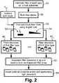
FIGURE 2 , manufacture of the filter array ofFIGURE 1 is diagrammatically shown. In an operationS1, a filter plate is fabricated on a bulk substrate for eachfilter element type 1, .., 5. Typically, this entails disposing the substrate (e.g. a glass substrate for some visible-range designs) in a deposition system and depositing the filter layers stack by sputtering, vacuum evaporation, plasma deposition, or another technique, with the thicknesses of the constituent layers of the filter stack of each filter plate designed to provide filter characteristics of the corresponding filter type. The result of this processing is a set offilter plates 50, e.g. five filter plates corresponding to filterelement types FIGURE 1 . - In an operationS2, the
filter plates 50 are then diced. The angled sidewalls are formed by dicing at angleθsub. Typically, the angleθ of lightL in the ambient is at least 5°, and more preferably at least 10°, although larger values for the design angleθ are contemplated, so that the angleθsub of the slanted sidewalls is at least 5°, and more preferably at least 9°. The dicing operationS2 can employ an angled-blade saw52 with the blade set tilted at the angleθsub, such as a semiconductor wafer dicing saw with an adjustable-angle cutting blade. Alternatively, the dicing can employ a laser dicing rig (not shown) with a tilted cutting laser beam angle. - In another approach, the cutting blade (or cutting laser beam) is kept perpendicular, and the filter plate is mounted on a wedge sub-mount54 for the dicing operationS2. In this approach the
wedge sub-mount 54 has a wedge angleθsub so that mounted filter plate is cut with the desired sidewall angleθsub. The dicing operationS2 producesfilter elements 601 of the first type from the first filter plate, filter elements of the second type from the second filter plate, and so on up to filterelements 60N of an Nth type (e.g. N = 5 inFIGURE 1 ). - In an operationS3, filter elements of the requisite types are then mounted in a bonding jig and glued together at the slanted sidewalls using adhesive or are otherwise bonded together to form the multispectral filter array. Optionally, in an operationS4 other components such as the entrance and/or exit
apertures light detectors 30 are added to the filter array to form a complete multispectral optical system. - With reference to
FIGURES 3 and4 , a side and a perspective view, respectively, of another illustrative embodiment is shown. InFIGURES 3 and4 the filter element substrates of the different filter element types are again distinguished by labels, here the labels "1" to "4". As in the embodiment ofFIGURE 1 , each filter element4 includes a filter layers stack112, for example embodied as optical coatings forming interference filters, disposed on afilter element substrate 114. In this embodiment entrance and exitapertures light entrance side 123 and on thelight exit side 124, respectively, as patterned dark mirror coatings deposited onto the boundaries between optical filter elements after the filter elements assembly operation. (Note that theentrance apertures 120 are labeled only inFIGURE 4 , while theexit apertures 122 are labeled only inFIGURE 3 ). As best seen inFIGURE 3 , this illustrative embodiment also employs smaller exit aperture openings compared with entrance aperture openings in order to reduce cross-talk. The perspective view ofFIGURE 4 shows the "stick" geometry of the optical filter elements of this one-dimensional filter array. As seen in bothFIGURES 3 and4 , the filter elements have slanted sidewalls140 (labeled only inFIGURE 3 ) corresponding to the slanted sidewalls40 of the embodiment ofFIGURE 1 . However, as further seen in bothFIGURES 3 and4 , the outermost optical filter elements of the filter array (those identified with filter type "1" and "4" inFIGURES 3 and4 ) have straight "outer"sidewalls 141 forming the edges of the assembled filter array. This can be advantageous insofar as the assembled filter array has the shape of a right-angled parallelepiped; however, the benefits of slanted sidewalls may be compromised for these outermost filter elements. (It should be noted that the filter array ofFIGURES 3 and4 includes only four filter elements; more typically, the filter array may include dozens or even hundreds of filter elements, and only the outermost filter element on each side has a straight sidewall). An alternative (not shown) is to employ optical filter elements with both sidewalls slanted, and to include additional triangular-shaped fill elements to provide the assembled filter geometry with straight outermost sidewalls. - In the illustrative examples, the filter array is a one-dimensional array,i.e. varying across the paper in the illustrative side view of
FIGURE 1 and not varying in the transverse direction, i.e. "into the page" in diagrammaticFIGURE 1 .See also the perspective view ofFIGURE 4 of the one-dimensional filter array ofFIGURES 3 and4 . In such a one-dimensional array, each filter element is elongated to form a filter element "stick", as best seen inFIGURE 4 . - However, it is also contemplated to have a two-dimensional array of filter elements. For a two-dimensional array, if the angle of incidenceθ of the light is only angled respective to one direction of the array, then the filter elements are suitably parallelogram-shaped in that direction, and rectangular in the transverse direction. However, it is also contemplated for the light to be angled in both directions of the ray, e.g. with angle-of-incidenceθx in the "x-direction" of the two-dimensional array and angle-of-incidenceθy in the "y-direction" of the two-dimensional array. In this case the filter elements are suitably parallelogram-shaped with sidewalls angledθx,sub in the "x-direction", and parallelogram-shaped with sidewalls angledθy,sub in the "y-direction".
Claims (7)
- An apparatus comprising:
an optical filter array with spectral selectivity comprising optical filter elements each including:a parallelogram-shaped filter element substrate (14) with parallel light entrance and light exit surfaces and parallel slanted sidewalls (40) slanted at an angle, andan interference filter disposed on one or both of the light entrance surface and the light exit surface, wherein the interference filter comprises a filter layer stack (12) including alternating layers of two or more materials with different refractive index values, and the filter layer stack (12) is supported by said filter element substrate (14) and is disposed on the entrance surface and/or on the exit surface of the filter element,the optical filter elements being bonded together at the slanted sidewalls (40) to form the optical filter array, wherein the optical filter elements are of different optical interference filter element types,the apparatus further comprising:an entrance aperture (20) located on the light entrance surfaces of the optical filter elements and having openings aligned with the light entrance surfaces of the optical filter elements; andan exit aperture (22) located on the light exit surfaces of the optical filter elements and having openings aligned with the light exit surfaces of the optical filter elements;wherein the exit aperture openings are laterally shifted relative to the entrance aperture openings to accommodate the slanted sidewalls (40) of the optical filter elements. - The apparatus of claim 1 wherein the openings of the exit aperture (22) are smaller than the openings of the entrance aperture (20), or wherein the openings of the exit aperture (22) are the same size as the openings of the entrance aperture (20).
- The apparatus of claim 1, wherein the interference filters of the optical filter elements comprise pass-band filters or notch filters operating in the visible spectrum, or
wherein the interference filters of the optical filter elements comprise pass-band filters or notch filters operating in the ultraviolet spectrum, or wherein the interference filters of the optical filter elements comprise pass-band filters or notch filters operating in the infrared spectrum. - The apparatus of claim 1 wherein the parallel slanted sidewalls (40) are slanted at an angle of at least 5°, or at an angle of at least 9°.
- A method to form an optical filter array according to claim 1, said method comprising:fabricating a plurality of optical filter plates of different optical interference filter types;dicing the optical filter plates to form optical interference filter elements with parallel slanted sidewalls (40) that are slanted at an angle;bonding the optical interference filter elements together at the parallel slanted sidewalls (40);an entrance aperture (20) located on the light entrance surfaces of the optical filter elements and having openings aligned with the light entrance surfaces of the optical filter elements is installed; andan exit aperture (22) located on the light exit surfaces of the optical filter elements and having openings aligned with the light exit surfaces of the optical filter elements is installed;wherein the exit aperture openings are laterally shifted relative to the entrance aperture openings to accommodate the slanted sidewalls (40) of the optical filter elements.
- The method of claim 5 wherein the dicing comprises dicing the optical filter plates using a saw or laser cutting beam tilted at the angle of the angled sidewalls, or wherein the dicing comprises dicing each optical filter plate with the optical filter plate mounted on a wedge sub-mount having a wedge angle equal to the angle of the slanted sidewalls.
- The method of claim 5, further comprising:
filtering light by illuminating the optical filter array with the light illuminating the optical filter array at an angle equal to or corresponding to the angle of the parallel slanted sidewalls (40).
Applications Claiming Priority (2)
| Application Number | Priority Date | Filing Date | Title |
|---|---|---|---|
| US201361812397P | 2013-04-16 | 2013-04-16 | |
| PCT/US2014/033784WO2014172195A2 (en) | 2013-04-16 | 2014-04-11 | Filter array with reduced stray light |
Publications (3)
| Publication Number | Publication Date |
|---|---|
| EP2987007A2 EP2987007A2 (en) | 2016-02-24 |
| EP2987007A4 EP2987007A4 (en) | 2016-12-07 |
| EP2987007B1true EP2987007B1 (en) | 2019-11-27 |
Family
ID=51686615
Family Applications (1)
| Application Number | Title | Priority Date | Filing Date |
|---|---|---|---|
| EP14785110.9AActiveEP2987007B1 (en) | 2013-04-16 | 2014-04-11 | Filter array with reduced stray light |
Country Status (3)
| Country | Link |
|---|---|
| US (1) | US10782459B2 (en) |
| EP (1) | EP2987007B1 (en) |
| WO (1) | WO2014172195A2 (en) |
Families Citing this family (8)
| Publication number | Priority date | Publication date | Assignee | Title |
|---|---|---|---|---|
| FI125514B (en)* | 2012-05-25 | 2015-11-13 | Valmet Automation Oy | Device and method for measuring a web containing cellulose and possibly lignin |
| JP7265865B2 (en)* | 2015-11-03 | 2023-04-27 | マテリオン コーポレイション | Filter array with focused light with reduced stray light |
| US10136077B1 (en)* | 2015-12-15 | 2018-11-20 | Lockheed Martin Corporation | Hyperspectral notch filter imaging |
| US10189239B2 (en) | 2015-12-16 | 2019-01-29 | Materion Corporation | Ability to three-dimensionally print an aperture mask on a multi spectral filter array |
| US10670779B1 (en) | 2016-09-08 | 2020-06-02 | Lockheed Martin Corporation | Multi-layered optical element |
| CN111465897A (en) | 2017-09-13 | 2020-07-28 | 美题隆公司 | Photoresist as opaque aperture mask on multispectral filter array |
| US11156753B2 (en)* | 2017-12-18 | 2021-10-26 | Viavi Solutions Inc. | Optical filters |
| CN109541801B (en)* | 2018-12-06 | 2021-04-13 | 中国工程物理研究院激光聚变研究中心 | Stray light pipe control system and method for high-power terminal optical system |
Citations (2)
| Publication number | Priority date | Publication date | Assignee | Title |
|---|---|---|---|---|
| US7433042B1 (en)* | 2003-12-05 | 2008-10-07 | Surface Optics Corporation | Spatially corrected full-cubed hyperspectral imager |
| US20120147228A1 (en)* | 2010-12-14 | 2012-06-14 | Duparre Jacques | Imaging systems with optical crosstalk suppression structures |
Family Cites Families (12)
| Publication number | Priority date | Publication date | Assignee | Title |
|---|---|---|---|---|
| US2708389A (en)* | 1951-01-09 | 1955-05-17 | Frederick W Kavanagh | Spectral wedge interference filter combined with purifying filters |
| US5096520A (en)* | 1990-08-01 | 1992-03-17 | Faris Sades M | Method for producing high efficiency polarizing filters |
| US5784507A (en)* | 1991-04-05 | 1998-07-21 | Holm-Kennedy; James W. | Integrated optical wavelength discrimination devices and methods for fabricating same |
| JPH0821748A (en) | 1994-07-07 | 1996-01-23 | Nippondenso Co Ltd | Display device |
| TW401530B (en)* | 1996-03-12 | 2000-08-11 | Seiko Epson Corp | Polarized light separation device, method of fabricating the same and projection display apparatus using the polarized light separation device |
| US6212312B1 (en)* | 1999-09-17 | 2001-04-03 | U.T. Battelle, Llc | Optical multiplexer/demultiplexer using resonant grating filters |
| US6726333B2 (en) | 2001-02-09 | 2004-04-27 | Reflectivity, Inc | Projection display with multiply filtered light |
| JP2004206057A (en)* | 2002-11-01 | 2004-07-22 | Omron Corp | Optical multiplexer / demultiplexer and method of manufacturing optical multiplexer / demultiplexer |
| US7038191B2 (en)* | 2003-03-13 | 2006-05-02 | The Boeing Company | Remote sensing apparatus and method |
| JP2007279692A (en) | 2006-03-13 | 2007-10-25 | Epson Toyocom Corp | Polarized light separating element and manufacturing method thereof |
| JP4924941B2 (en) | 2006-10-13 | 2012-04-25 | Nltテクノロジー株式会社 | Optical elements, illumination optical devices, display devices, and electronic devices. |
| JP2014095843A (en)* | 2012-11-12 | 2014-05-22 | Sumitomo Electric Ind Ltd | Optical multiplexer/demultiplexer and method of manufacturing the same, and optical communication module |
- 2014
- 2014-04-11USUS14/250,553patent/US10782459B2/enactiveActive
- 2014-04-11EPEP14785110.9Apatent/EP2987007B1/enactiveActive
- 2014-04-11WOPCT/US2014/033784patent/WO2014172195A2/enactiveApplication Filing
Patent Citations (2)
| Publication number | Priority date | Publication date | Assignee | Title |
|---|---|---|---|---|
| US7433042B1 (en)* | 2003-12-05 | 2008-10-07 | Surface Optics Corporation | Spatially corrected full-cubed hyperspectral imager |
| US20120147228A1 (en)* | 2010-12-14 | 2012-06-14 | Duparre Jacques | Imaging systems with optical crosstalk suppression structures |
Non-Patent Citations (1)
| Title |
|---|
| ANONYMOUS: "Anti-reflective coating - Wikipedia, the free encyclopedia", 19 January 2013 (2013-01-19), XP055595673, Retrieved from the Internet <URL:https://web.archive.org/web/20130119142642/https://en.wikipedia.org/wiki/Anti-reflective_coating> [retrieved on 20190611]* |
Also Published As
| Publication number | Publication date |
|---|---|
| EP2987007A4 (en) | 2016-12-07 |
| US20140307309A1 (en) | 2014-10-16 |
| EP2987007A2 (en) | 2016-02-24 |
| US10782459B2 (en) | 2020-09-22 |
| WO2014172195A2 (en) | 2014-10-23 |
| WO2014172195A3 (en) | 2015-02-19 |
Similar Documents
| Publication | Publication Date | Title |
|---|---|---|
| EP2987007B1 (en) | Filter array with reduced stray light | |
| US20210028213A1 (en) | Variable optical filter and a wavelength-selective sensor based thereon | |
| US10488568B2 (en) | Filter array with reduced stray focused light | |
| KR20180082508A (en) | Optical detection device and method for manufacturing optical detection device | |
| US12345903B2 (en) | Photo resist as opaque aperture mask on multispectral filter arrays | |
| US10976200B2 (en) | Optical sensing device and method for manufacturing an optical sensing device | |
| JP6836428B2 (en) | Spectral filter and spectrophotometer | |
| US7508567B1 (en) | Metal etalon with enhancing stack | |
| US8288708B2 (en) | Optical filter | |
| JP6806603B2 (en) | Spectral filter and spectrophotometer | |
| US20250155621A1 (en) | Multilayer optical coating with metastructures | |
| CN217542855U (en) | Tandem grating spectrometer | |
| JP6806604B2 (en) | Spectral filter unit and spectrophotometer | |
| WO2025106681A1 (en) | Multilayer optical coating with metastructures |
Legal Events
| Date | Code | Title | Description |
|---|---|---|---|
| PUAI | Public reference made under article 153(3) epc to a published international application that has entered the european phase | Free format text:ORIGINAL CODE: 0009012 | |
| 17P | Request for examination filed | Effective date:20151030 | |
| AK | Designated contracting states | Kind code of ref document:A2 Designated state(s):AL AT BE BG CH CY CZ DE DK EE ES FI FR GB GR HR HU IE IS IT LI LT LU LV MC MK MT NL NO PL PT RO RS SE SI SK SM TR | |
| AX | Request for extension of the european patent | Extension state:BA ME | |
| DAX | Request for extension of the european patent (deleted) | ||
| A4 | Supplementary search report drawn up and despatched | Effective date:20161109 | |
| RIC1 | Information provided on ipc code assigned before grant | Ipc:G02B 27/00 20060101ALI20161103BHEP Ipc:G02B 5/28 20060101AFI20161103BHEP | |
| STAA | Information on the status of an ep patent application or granted ep patent | Free format text:STATUS: EXAMINATION IS IN PROGRESS | |
| 17Q | First examination report despatched | Effective date:20170907 | |
| REG | Reference to a national code | Ref country code:DE Ref legal event code:R079 Ref document number:602014057540 Country of ref document:DE Free format text:PREVIOUS MAIN CLASS: G02B0005280000 Ipc:G02B0027280000 | |
| GRAP | Despatch of communication of intention to grant a patent | Free format text:ORIGINAL CODE: EPIDOSNIGR1 | |
| STAA | Information on the status of an ep patent application or granted ep patent | Free format text:STATUS: GRANT OF PATENT IS INTENDED | |
| RIC1 | Information provided on ipc code assigned before grant | Ipc:G02B 5/20 20060101ALI20190611BHEP Ipc:G02B 27/28 20060101AFI20190611BHEP | |
| INTG | Intention to grant announced | Effective date:20190711 | |
| GRAS | Grant fee paid | Free format text:ORIGINAL CODE: EPIDOSNIGR3 | |
| GRAA | (expected) grant | Free format text:ORIGINAL CODE: 0009210 | |
| STAA | Information on the status of an ep patent application or granted ep patent | Free format text:STATUS: THE PATENT HAS BEEN GRANTED | |
| AK | Designated contracting states | Kind code of ref document:B1 Designated state(s):AL AT BE BG CH CY CZ DE DK EE ES FI FR GB GR HR HU IE IS IT LI LT LU LV MC MK MT NL NO PL PT RO RS SE SI SK SM TR | |
| REG | Reference to a national code | Ref country code:GB Ref legal event code:FG4D | |
| REG | Reference to a national code | Ref country code:CH Ref legal event code:EP | |
| REG | Reference to a national code | Ref country code:AT Ref legal event code:REF Ref document number:1207359 Country of ref document:AT Kind code of ref document:T Effective date:20191215 | |
| REG | Reference to a national code | Ref country code:DE Ref legal event code:R096 Ref document number:602014057540 Country of ref document:DE | |
| REG | Reference to a national code | Ref country code:IE Ref legal event code:FG4D | |
| REG | Reference to a national code | Ref country code:NL Ref legal event code:MP Effective date:20191127 | |
| REG | Reference to a national code | Ref country code:LT Ref legal event code:MG4D | |
| PG25 | Lapsed in a contracting state [announced via postgrant information from national office to epo] | Ref country code:NL Free format text:LAPSE BECAUSE OF FAILURE TO SUBMIT A TRANSLATION OF THE DESCRIPTION OR TO PAY THE FEE WITHIN THE PRESCRIBED TIME-LIMIT Effective date:20191127 Ref country code:LT Free format text:LAPSE BECAUSE OF FAILURE TO SUBMIT A TRANSLATION OF THE DESCRIPTION OR TO PAY THE FEE WITHIN THE PRESCRIBED TIME-LIMIT Effective date:20191127 Ref country code:NO Free format text:LAPSE BECAUSE OF FAILURE TO SUBMIT A TRANSLATION OF THE DESCRIPTION OR TO PAY THE FEE WITHIN THE PRESCRIBED TIME-LIMIT Effective date:20200227 Ref country code:GR Free format text:LAPSE BECAUSE OF FAILURE TO SUBMIT A TRANSLATION OF THE DESCRIPTION OR TO PAY THE FEE WITHIN THE PRESCRIBED TIME-LIMIT Effective date:20200228 Ref country code:BG Free format text:LAPSE BECAUSE OF FAILURE TO SUBMIT A TRANSLATION OF THE DESCRIPTION OR TO PAY THE FEE WITHIN THE PRESCRIBED TIME-LIMIT Effective date:20200227 Ref country code:FI Free format text:LAPSE BECAUSE OF FAILURE TO SUBMIT A TRANSLATION OF THE DESCRIPTION OR TO PAY THE FEE WITHIN THE PRESCRIBED TIME-LIMIT Effective date:20191127 Ref country code:LV Free format text:LAPSE BECAUSE OF FAILURE TO SUBMIT A TRANSLATION OF THE DESCRIPTION OR TO PAY THE FEE WITHIN THE PRESCRIBED TIME-LIMIT Effective date:20191127 Ref country code:SE Free format text:LAPSE BECAUSE OF FAILURE TO SUBMIT A TRANSLATION OF THE DESCRIPTION OR TO PAY THE FEE WITHIN THE PRESCRIBED TIME-LIMIT Effective date:20191127 | |
| PG25 | Lapsed in a contracting state [announced via postgrant information from national office to epo] | Ref country code:RS Free format text:LAPSE BECAUSE OF FAILURE TO SUBMIT A TRANSLATION OF THE DESCRIPTION OR TO PAY THE FEE WITHIN THE PRESCRIBED TIME-LIMIT Effective date:20191127 Ref country code:IS Free format text:LAPSE BECAUSE OF FAILURE TO SUBMIT A TRANSLATION OF THE DESCRIPTION OR TO PAY THE FEE WITHIN THE PRESCRIBED TIME-LIMIT Effective date:20200327 Ref country code:HR Free format text:LAPSE BECAUSE OF FAILURE TO SUBMIT A TRANSLATION OF THE DESCRIPTION OR TO PAY THE FEE WITHIN THE PRESCRIBED TIME-LIMIT Effective date:20191127 | |
| PG25 | Lapsed in a contracting state [announced via postgrant information from national office to epo] | Ref country code:AL Free format text:LAPSE BECAUSE OF FAILURE TO SUBMIT A TRANSLATION OF THE DESCRIPTION OR TO PAY THE FEE WITHIN THE PRESCRIBED TIME-LIMIT Effective date:20191127 | |
| PG25 | Lapsed in a contracting state [announced via postgrant information from national office to epo] | Ref country code:ES Free format text:LAPSE BECAUSE OF FAILURE TO SUBMIT A TRANSLATION OF THE DESCRIPTION OR TO PAY THE FEE WITHIN THE PRESCRIBED TIME-LIMIT Effective date:20191127 Ref country code:CZ Free format text:LAPSE BECAUSE OF FAILURE TO SUBMIT A TRANSLATION OF THE DESCRIPTION OR TO PAY THE FEE WITHIN THE PRESCRIBED TIME-LIMIT Effective date:20191127 Ref country code:RO Free format text:LAPSE BECAUSE OF FAILURE TO SUBMIT A TRANSLATION OF THE DESCRIPTION OR TO PAY THE FEE WITHIN THE PRESCRIBED TIME-LIMIT Effective date:20191127 Ref country code:DK Free format text:LAPSE BECAUSE OF FAILURE TO SUBMIT A TRANSLATION OF THE DESCRIPTION OR TO PAY THE FEE WITHIN THE PRESCRIBED TIME-LIMIT Effective date:20191127 Ref country code:PT Free format text:LAPSE BECAUSE OF FAILURE TO SUBMIT A TRANSLATION OF THE DESCRIPTION OR TO PAY THE FEE WITHIN THE PRESCRIBED TIME-LIMIT Effective date:20200419 Ref country code:EE Free format text:LAPSE BECAUSE OF FAILURE TO SUBMIT A TRANSLATION OF THE DESCRIPTION OR TO PAY THE FEE WITHIN THE PRESCRIBED TIME-LIMIT Effective date:20191127 | |
| REG | Reference to a national code | Ref country code:DE Ref legal event code:R097 Ref document number:602014057540 Country of ref document:DE | |
| PG25 | Lapsed in a contracting state [announced via postgrant information from national office to epo] | Ref country code:SK Free format text:LAPSE BECAUSE OF FAILURE TO SUBMIT A TRANSLATION OF THE DESCRIPTION OR TO PAY THE FEE WITHIN THE PRESCRIBED TIME-LIMIT Effective date:20191127 Ref country code:SM Free format text:LAPSE BECAUSE OF FAILURE TO SUBMIT A TRANSLATION OF THE DESCRIPTION OR TO PAY THE FEE WITHIN THE PRESCRIBED TIME-LIMIT Effective date:20191127 | |
| REG | Reference to a national code | Ref country code:AT Ref legal event code:MK05 Ref document number:1207359 Country of ref document:AT Kind code of ref document:T Effective date:20191127 | |
| PLBE | No opposition filed within time limit | Free format text:ORIGINAL CODE: 0009261 | |
| STAA | Information on the status of an ep patent application or granted ep patent | Free format text:STATUS: NO OPPOSITION FILED WITHIN TIME LIMIT | |
| 26N | No opposition filed | Effective date:20200828 | |
| PG25 | Lapsed in a contracting state [announced via postgrant information from national office to epo] | Ref country code:SI Free format text:LAPSE BECAUSE OF FAILURE TO SUBMIT A TRANSLATION OF THE DESCRIPTION OR TO PAY THE FEE WITHIN THE PRESCRIBED TIME-LIMIT Effective date:20191127 Ref country code:AT Free format text:LAPSE BECAUSE OF FAILURE TO SUBMIT A TRANSLATION OF THE DESCRIPTION OR TO PAY THE FEE WITHIN THE PRESCRIBED TIME-LIMIT Effective date:20191127 Ref country code:PL Free format text:LAPSE BECAUSE OF FAILURE TO SUBMIT A TRANSLATION OF THE DESCRIPTION OR TO PAY THE FEE WITHIN THE PRESCRIBED TIME-LIMIT Effective date:20191127 Ref country code:MC Free format text:LAPSE BECAUSE OF FAILURE TO SUBMIT A TRANSLATION OF THE DESCRIPTION OR TO PAY THE FEE WITHIN THE PRESCRIBED TIME-LIMIT Effective date:20191127 | |
| REG | Reference to a national code | Ref country code:CH Ref legal event code:PL | |
| PG25 | Lapsed in a contracting state [announced via postgrant information from national office to epo] | Ref country code:LI Free format text:LAPSE BECAUSE OF NON-PAYMENT OF DUE FEES Effective date:20200430 Ref country code:CH Free format text:LAPSE BECAUSE OF NON-PAYMENT OF DUE FEES Effective date:20200430 Ref country code:IT Free format text:LAPSE BECAUSE OF FAILURE TO SUBMIT A TRANSLATION OF THE DESCRIPTION OR TO PAY THE FEE WITHIN THE PRESCRIBED TIME-LIMIT Effective date:20191127 Ref country code:LU Free format text:LAPSE BECAUSE OF NON-PAYMENT OF DUE FEES Effective date:20200411 | |
| REG | Reference to a national code | Ref country code:BE Ref legal event code:MM Effective date:20200430 | |
| PG25 | Lapsed in a contracting state [announced via postgrant information from national office to epo] | Ref country code:BE Free format text:LAPSE BECAUSE OF NON-PAYMENT OF DUE FEES Effective date:20200430 | |
| PG25 | Lapsed in a contracting state [announced via postgrant information from national office to epo] | Ref country code:IE Free format text:LAPSE BECAUSE OF NON-PAYMENT OF DUE FEES Effective date:20200411 | |
| PG25 | Lapsed in a contracting state [announced via postgrant information from national office to epo] | Ref country code:TR Free format text:LAPSE BECAUSE OF FAILURE TO SUBMIT A TRANSLATION OF THE DESCRIPTION OR TO PAY THE FEE WITHIN THE PRESCRIBED TIME-LIMIT Effective date:20191127 Ref country code:MT Free format text:LAPSE BECAUSE OF FAILURE TO SUBMIT A TRANSLATION OF THE DESCRIPTION OR TO PAY THE FEE WITHIN THE PRESCRIBED TIME-LIMIT Effective date:20191127 Ref country code:CY Free format text:LAPSE BECAUSE OF FAILURE TO SUBMIT A TRANSLATION OF THE DESCRIPTION OR TO PAY THE FEE WITHIN THE PRESCRIBED TIME-LIMIT Effective date:20191127 | |
| PG25 | Lapsed in a contracting state [announced via postgrant information from national office to epo] | Ref country code:MK Free format text:LAPSE BECAUSE OF FAILURE TO SUBMIT A TRANSLATION OF THE DESCRIPTION OR TO PAY THE FEE WITHIN THE PRESCRIBED TIME-LIMIT Effective date:20191127 | |
| P01 | Opt-out of the competence of the unified patent court (upc) registered | Effective date:20230530 | |
| PGFP | Annual fee paid to national office [announced via postgrant information from national office to epo] | Ref country code:DE Payment date:20250429 Year of fee payment:12 | |
| PGFP | Annual fee paid to national office [announced via postgrant information from national office to epo] | Ref country code:GB Payment date:20250423 Year of fee payment:12 | |
| PGFP | Annual fee paid to national office [announced via postgrant information from national office to epo] | Ref country code:FR Payment date:20250428 Year of fee payment:12 |