EP2975767B1 - A switched mode power supply and lighting circuit - Google Patents
A switched mode power supply and lighting circuitDownload PDFInfo
- Publication number
- EP2975767B1 EP2975767B1EP14177479.4AEP14177479AEP2975767B1EP 2975767 B1EP2975767 B1EP 2975767B1EP 14177479 AEP14177479 AEP 14177479AEP 2975767 B1EP2975767 B1EP 2975767B1
- Authority
- EP
- European Patent Office
- Prior art keywords
- switch
- power switch
- current
- capacitor
- terminal
- Prior art date
- Legal status (The legal status is an assumption and is not a legal conclusion. Google has not performed a legal analysis and makes no representation as to the accuracy of the status listed.)
- Active
Links
Images


Classifications
- H—ELECTRICITY
- H05—ELECTRIC TECHNIQUES NOT OTHERWISE PROVIDED FOR
- H05B—ELECTRIC HEATING; ELECTRIC LIGHT SOURCES NOT OTHERWISE PROVIDED FOR; CIRCUIT ARRANGEMENTS FOR ELECTRIC LIGHT SOURCES, IN GENERAL
- H05B45/00—Circuit arrangements for operating light-emitting diodes [LED]
- H05B45/30—Driver circuits
- H05B45/37—Converter circuits
- H05B45/3725—Switched mode power supply [SMPS]
- G—PHYSICS
- G06—COMPUTING OR CALCULATING; COUNTING
- G06F—ELECTRIC DIGITAL DATA PROCESSING
- G06F1/00—Details not covered by groups G06F3/00 - G06F13/00 and G06F21/00
- G06F1/26—Power supply means, e.g. regulation thereof
- G06F1/32—Means for saving power
- G06F1/3203—Power management, i.e. event-based initiation of a power-saving mode
- G06F1/3234—Power saving characterised by the action undertaken
- G06F1/3243—Power saving in microcontroller unit
- G—PHYSICS
- G06—COMPUTING OR CALCULATING; COUNTING
- G06F—ELECTRIC DIGITAL DATA PROCESSING
- G06F1/00—Details not covered by groups G06F3/00 - G06F13/00 and G06F21/00
- G06F1/26—Power supply means, e.g. regulation thereof
- G06F1/32—Means for saving power
- G06F1/3203—Power management, i.e. event-based initiation of a power-saving mode
- G06F1/3234—Power saving characterised by the action undertaken
- G06F1/3287—Power saving characterised by the action undertaken by switching off individual functional units in the computer system
- H—ELECTRICITY
- H02—GENERATION; CONVERSION OR DISTRIBUTION OF ELECTRIC POWER
- H02M—APPARATUS FOR CONVERSION BETWEEN AC AND AC, BETWEEN AC AND DC, OR BETWEEN DC AND DC, AND FOR USE WITH MAINS OR SIMILAR POWER SUPPLY SYSTEMS; CONVERSION OF DC OR AC INPUT POWER INTO SURGE OUTPUT POWER; CONTROL OR REGULATION THEREOF
- H02M1/00—Details of apparatus for conversion
- H02M1/08—Circuits specially adapted for the generation of control voltages for semiconductor devices incorporated in static converters
- H02M1/088—Circuits specially adapted for the generation of control voltages for semiconductor devices incorporated in static converters for the simultaneous control of series or parallel connected semiconductor devices
- H—ELECTRICITY
- H02—GENERATION; CONVERSION OR DISTRIBUTION OF ELECTRIC POWER
- H02M—APPARATUS FOR CONVERSION BETWEEN AC AND AC, BETWEEN AC AND DC, OR BETWEEN DC AND DC, AND FOR USE WITH MAINS OR SIMILAR POWER SUPPLY SYSTEMS; CONVERSION OF DC OR AC INPUT POWER INTO SURGE OUTPUT POWER; CONTROL OR REGULATION THEREOF
- H02M1/00—Details of apparatus for conversion
- H02M1/36—Means for starting or stopping converters
- H—ELECTRICITY
- H02—GENERATION; CONVERSION OR DISTRIBUTION OF ELECTRIC POWER
- H02M—APPARATUS FOR CONVERSION BETWEEN AC AND AC, BETWEEN AC AND DC, OR BETWEEN DC AND DC, AND FOR USE WITH MAINS OR SIMILAR POWER SUPPLY SYSTEMS; CONVERSION OF DC OR AC INPUT POWER INTO SURGE OUTPUT POWER; CONTROL OR REGULATION THEREOF
- H02M3/00—Conversion of DC power input into DC power output
- H02M3/02—Conversion of DC power input into DC power output without intermediate conversion into AC
- H02M3/04—Conversion of DC power input into DC power output without intermediate conversion into AC by static converters
- H02M3/10—Conversion of DC power input into DC power output without intermediate conversion into AC by static converters using discharge tubes with control electrode or semiconductor devices with control electrode
- H02M3/145—Conversion of DC power input into DC power output without intermediate conversion into AC by static converters using discharge tubes with control electrode or semiconductor devices with control electrode using devices of a triode or transistor type requiring continuous application of a control signal
- H02M3/155—Conversion of DC power input into DC power output without intermediate conversion into AC by static converters using discharge tubes with control electrode or semiconductor devices with control electrode using devices of a triode or transistor type requiring continuous application of a control signal using semiconductor devices only
- H—ELECTRICITY
- H03—ELECTRONIC CIRCUITRY
- H03K—PULSE TECHNIQUE
- H03K17/00—Electronic switching or gating, i.e. not by contact-making and –breaking
- H03K17/16—Modifications for eliminating interference voltages or currents
- H—ELECTRICITY
- H03—ELECTRONIC CIRCUITRY
- H03K—PULSE TECHNIQUE
- H03K17/00—Electronic switching or gating, i.e. not by contact-making and –breaking
- H03K17/10—Modifications for increasing the maximum permissible switched voltage
- H03K17/107—Modifications for increasing the maximum permissible switched voltage in composite switches
- H—ELECTRICITY
- H03—ELECTRONIC CIRCUITRY
- H03K—PULSE TECHNIQUE
- H03K2217/00—Indexing scheme related to electronic switching or gating, i.e. not by contact-making or -breaking covered by H03K17/00
- H03K2217/0081—Power supply means, e.g. to the switch driver
- H—ELECTRICITY
- H05—ELECTRIC TECHNIQUES NOT OTHERWISE PROVIDED FOR
- H05B—ELECTRIC HEATING; ELECTRIC LIGHT SOURCES NOT OTHERWISE PROVIDED FOR; CIRCUIT ARRANGEMENTS FOR ELECTRIC LIGHT SOURCES, IN GENERAL
- H05B45/00—Circuit arrangements for operating light-emitting diodes [LED]
- H05B45/30—Driver circuits
- H05B45/37—Converter circuits
- H05B45/3725—Switched mode power supply [SMPS]
- H05B45/375—Switched mode power supply [SMPS] using buck topology
- H—ELECTRICITY
- H05—ELECTRIC TECHNIQUES NOT OTHERWISE PROVIDED FOR
- H05B—ELECTRIC HEATING; ELECTRIC LIGHT SOURCES NOT OTHERWISE PROVIDED FOR; CIRCUIT ARRANGEMENTS FOR ELECTRIC LIGHT SOURCES, IN GENERAL
- H05B45/00—Circuit arrangements for operating light-emitting diodes [LED]
- H05B45/30—Driver circuits
- H05B45/37—Converter circuits
- H05B45/3725—Switched mode power supply [SMPS]
- H05B45/38—Switched mode power supply [SMPS] using boost topology
- H—ELECTRICITY
- H05—ELECTRIC TECHNIQUES NOT OTHERWISE PROVIDED FOR
- H05B—ELECTRIC HEATING; ELECTRIC LIGHT SOURCES NOT OTHERWISE PROVIDED FOR; CIRCUIT ARRANGEMENTS FOR ELECTRIC LIGHT SOURCES, IN GENERAL
- H05B45/00—Circuit arrangements for operating light-emitting diodes [LED]
- H05B45/30—Driver circuits
- H05B45/37—Converter circuits
- H05B45/3725—Switched mode power supply [SMPS]
- H05B45/385—Switched mode power supply [SMPS] using flyback topology
Definitions
- This disclosurerelates to switched mode power supplies (SMPS) and to lighting circuit comprising such SMPS.
- SMPSswitched mode power supplies
- the switching elementcomprises separate but series-connected power switch and control switches. This is currently most frequently the case, and often may be necessary, in designs in which the power switch is a high-voltage bipolar junction transistor. However it should be mentioned at the outset, that a separate power switch and control switch may also be used in designs in which the power switch is a high-voltage MOSFET. Since separate control and power switches are most commonly used with bipolar junction transistors, designs utilising these two switches are often loosely referred to as emitter switched converters. Relative to high-voltage MOSFETs, high-voltage bipolar devices may be significantly cheaper, but since they suffer the drawback of low voltage amplification, they typically require a large base driver current.
- Switched mode power suppliesare typically operated under the control of a controller, which controls the timing of the switching of the switching element.
- the switching elementmay switch the control switch, and the power switch is arranged and configured to switch following the operation of the control switch.
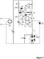
- FIG. 1A schematic of a SMPS connected to an AC mains 120 through rectifier B1 and input smoothing capacitor C1, and driving LEDs is shown in figure 1 .
- the SMPSis a buck converter.
- the convertercomprises a series arrangement of a control switch S1, a power switch S2, and an inductor L1.
- the loadwhich is shown as a series string of LEDs is connected in series with the inductor L1.
- power switch S2is a bipolar transistor which requires a relatively high base current.
- the base terminal of the switch S2is connected to the smoothed rectified mains input through a resistor R1 and a parallel arrangement of a diode D3 and a resistor R4.
- the value of resistor R4is chosen so as to set the required appropriate base current for the power switch S2, and diode D3 is provided so as to ensure that S2 can be switched off quickly.
- the SMPScomprises a controller 110 which has a supply terminal 114 and ground terminal 112. A capacitor C2 is connected across these terminals to provide a supply voltage Vcc to the controller 110. Also shown is a sense resistor R2 which is connected to the controller and used to sense the current through the inductor in order to control the switching.
- VccAs soon as Vcc rises above the start-up voltage, the controller starts switching.
- a switching mode power supply controllerconsumes more supply current in switching state than in non-switching state. For example additional supply current is needed to drive the power switch.
- VstartWhen the current through R1 is just enough to charge C2 to the start-up voltage level (Vstart), it may not be enough to supply the SMPS during operation. The supply voltage would then drop and could reach a voltage level were the SMPS cannot work properly anymore.
- Vstopunder-voltage-lock-out voltage
- a take-over supplycomprising diode D2 and resistor R3 is added to provide additional current as soon as the converter starts switching and the LED voltage rises above the Vcc level.
- a take-over supplycomprising diode D2 and resistor R3 is added to provide additional current as soon as the converter starts switching and the LED voltage rises above the Vcc level.
- an auxiliary winding on the primary side of the transformermay be included to provide power to the controller, once the SMPS is in operation.
- United States Patent Application publication number US2010/0309689 A1discloses a bootstrap circuit for a switch mode power supply, a controller for a switch mode voltage converter, a switch mode flyback converter comprising the bootstrap circuit, a switch mode forward converter comprising the bootstrap circuit, and a method of bootstrapping a switch mode power converter.
- the bootstrap circuitcomprises: a current bleed impedance (Rht 1 ) to bleed current from an input power supply (VH+); circuitry to deliver current from the input power supply (VH+) via the current bleed impedance (Rht 1 ) to the base of a power switch (Q 1 ) such that the power switch (Q 1 ) is operable to amplify the current delivered from the internal power supply; a passive circuit (Dst) to provide the amplified current to a reservoir capacitor (Cdd); and the passive circuit element (Dst) further to substantially block reverse current flow from the supply input (Vdd) to the emitter of the power switch (Q 1 ).
- a current bleed impedance (Rht 1 )to bleed current from an input power supply (VH+)
- circuitryto deliver current from the input power supply (VH+) via the current bleed impedance (Rht 1 ) to the base of a power switch (Q 1 ) such that the power switch (Q 1
- a switched mode power supplyfor converting an input voltage and comprising: a series arrangement of an inductor, a power switch and a control switch for controlling the power switch; a controller configured to control the control switch and having a supply terminal and a ground terminal; a capacitor coupled between the controller ground terminal and supply terminal and for providing power to the controller; a first current path arranged to provide charge to the capacitor only when the control switch is open and the power switch is closed; a connectable second current path arranged to draw current from the control terminal of the power switch thereby opening the power switch, and a connection switch configured to connect the second current path in response to a voltage across the capacitor exceeding a threshold voltage.
- chargemay be provided to the capacitor, from the input (such as a rectified mains).
- the capacitoris used to power the controller, it may be possible to thereby avoid the need for an auxiliary power supply for the controller.
- the power switchis a bipolar junction transistor and the current drawn from the control terminal of the power switch is provided by a base charge of the transistor in an on-state.
- the base charge in a bipolar transistoris generally much higher than any charge on the gate of a MOSFET.
- the switched mode power supplyfurther comprises a further current path through the base of the power switch thereby enabling a start-up of the switched mode power supply.
- the second current pathis a recycling path arranged to draw current from the control terminal of the power switch to charge the capacitor.
- the base chargemay be relatively high, and thus by recycling this charge to charge the capacitor, it might be possible to achieve a significant increase in efficiency of the circuit.
- the switched mode power supplyfurther comprises a current path between the power switch control terminal and a positive terminal of the input voltage, which may be a rectified mains.
- the current path arranged to provide charge to the capacitor when the power switch is closedcomprises a diode.
- the switched mode power supplymay be a buck converter and be arranged for connection of a load in series with the series arrangement.
- the switched mode power supplymay be a boost converter and be arranged for connection of a load in parallel with the control switch and power switch in series.
- the switched mode power supplymay be a flyback converter wherein the inductor is a primary winding of a transformer, and the switch mode power supply is arranged for connection of a load to a secondary winding of the transformer.
- a lighting circuitcomprising a switch mode power supply has described above, and the load, wherein the load is a string of LEDs.
- the input voltagemay be smoothed rectified mains supply.
- a method of controlling a switched mode power supplycomprising a series arrangement of a power switch, a control switch and an inductor, the arrangement being connected across a positive and a negative terminal of an input voltage, such as for example a rectified and smoothed mains; a controller having a supply terminal and a ground terminal; and a capacitor coupled between a ground terminal and a supply terminal of the controller and for providing power to the controller; the method comprising; operating the controller to periodically open and close the control switch; providing charge to the capacitor through a first current path only when the control switch is open and the power switch is closed; and in response to a voltage across the capacitor exceeding a threshold voltage, operating a connection switch to connect a second path thereby drawing current from the control terminal of the power switch thereby opening the power switch.
- FIG. 2shows a switched mode power supply according to embodiments, for converting an input voltage.
- the SMPSwhich may also be referred to as a switched mode power converter, comprises: a series arrangement of an inductor L1, a power switch S2, a control switch S1 for controlling the power switch; a controller 110 configured to control the control switch and having a supply terminal 112 and a ground terminal 114; a capacitor C2 coupled between the controller ground terminal and supply terminal and for providing power to the controller; a first current path 240 arranged to provide charge to the capacitor only when the control switch is open and the power switch is closed; a connectable second current path 250 arranged to draw current from the control terminal of the power switch thereby opening the power switch, and a connection switch S3 configured to connect the second current path in the event that, or in response to, a voltage across the capacitor exceeds a threshold voltage.
- the SMPSis shown to be connected to the AC mains through rectifier B1 and input smoothing capacitor C1, and drives a string of LEDs 230.
- the convertercomprises a series arrangement of a control switch S1, a power switch S2, and an inductor L1 (not necessarily in that order).
- the string of LEDscomprises the load, and is connected in series with the inductor L1.
- the controller 110has supply and ground terminals 114, 112. Capacitor C2 is connected across these terminals and provides a supply voltage Vcc to the controller 110.
- a sense resistor R2which is connected to the controller and used to sense the current through the inductor in order to control the switching.
- Power switch S2is shown as a bipolar transistor.
- a sense resistormay not be required in embodiments in which other means are used to determine the appropriate switching moment of the control or power switches.
- the power switch S2At start-up (which will be considered in more detail below), its base terminal is connected to the smoothed rectified mains input through resistor R1.
- resistor R1During normal operation, current is provided to the base through R4.
- a relatively small amount of currentmay also be provided through R1 - in a typical example, the base current is more than 10mA, and R4 thus has to be able supply this magnitude of current, whereas the value of R1 may be chosen to be able to supply only 1 mA or less.
- Discharging of the base charge through R4 when the power switch is open,is prevented by a diode D5; however, when the power switch is closed but the control switch is open, current can flow through D4, which thus is in the first current path, to charge the capacitor C2.
- the connectable current path, through which the base charge may discharge,is provided through diode D3 which connects the base terminal of the power switch to C2 via a switch S3.
- the connection status of this second current pathis thus determined by the closed/open status of switch S3.
- Switch S3may therefore be described as a connection switch.
- the status of this connection switchmay be determined, as shown in these embodiments, by a comparator 220, which compares the voltage at the base of the power switch with a threshold voltage.
- R4is chosen to provide the required level of base current for the power switch S2:
- Vcc13V
- Ube(S2)is the base emitter voltage across the power switch S2
- U(R2)is the voltage across the resistor R2 and assuming that the voltage drop across S1 is small and the peak voltage across R2 is 1Volt.
- Figure 3shows various signals associated with the operation of a switched mode power supply as described above with reference to figure 2 , over one-and-a-half switching cycles. Key moments in the switching cycles are shown at t0 - both switches closed, t1 - control switch S1 opens, t2 - power switch S2 starts to open, and t3 - power switch S3 completely open.
- t4represents the start of a new cycle and is thus equivalent to t0.
- the figureshows, from the top: the conduction status 310 of control switch S1, the conduction status 315 of power switch S2, the conduction status 320 of connection switch S3, the collector current 325 in power switch S2, the base current 330 of power switch S2, the current 335 through control switch S1, the current 340 through diode D4, the current 345 through the inductor L1, the voltage 350 at the base of S2, and the voltage Vcc 355 at the capacitor C2.
- control switch S1is switched on by controller 110.
- Control switch S1switches power switch S2 on via the emitter.
- the current in the switches and inductor L1increases linearly. Due to the base current and also the controller supply current, the Vcc voltage drops.
- control switch S1is switched off.
- the base (and emitter) voltage of power switch S2rise until diode D4 starts conducting.
- the currentthen flows through diode D4, charging Vcc capacitor C2.
- the Vcc voltage, emitter voltage and base voltagerise until the base voltage reaches the reference voltage Vref at moment t2.
- Connection switch S3is then closed and the base charge of power switch S2 is conducted to the capacitor C2 via connection switch S3 and diode D3.
- the signals shown in figure 3correspond to boundary mode conduction. That is to say, as soon as the inductor current 345 falls to 0, a new primary stroke starts.
- embodimentsmay also use either continuous conduction mode or discontinuous conduction mode.
- continuous conduction modethe inductor current does not return to zero, but the subsequent primary stroke starts earlier. This is shown at 390 in the upper cutaway section of figure 3 .
- discontinuous conduction modethe inductor current returns to 0, and there is a subsequent gap before the next subsequent primary stroke commences. This gap is shown at 395 in the lower cutaway in figure 3 .
- Figures 4-7show the current flow through the circuit depicted in figure 2 , at various times during the switching cycle: Figure 4 shows the current flow as dashed line 410 through the control and power switches S1 and S2 during interval t0-t1.
- the arrangement according to embodimentsenables charging of the capacitor C2 thereby providing power to the controller, during normal operation. This occurs during the period t1-2 shown in figure 3 .
- This current flowis shown as dashed line 510 in figure 5 .
- Thisis without the requirement for a separate auxiliary power supply (such as R3 and D2 shown in figure 1 ). It therefore may be possible to avoid the complexity and expense of a separate auxiliary power supply for the controller.
- this supplymay be very efficient. It should be noted that this effect is not the same as a linear regulator: in particular, S2 does not operate in linear mode - which is the case for a linear regulator supplying an SMPS.
- the supply voltage Vccis regulated according to the 'Vref' voltage: that is to say, as soon as Vcc exceeds V(ref), less the sum of the forward voltage U(D4) across D4 and the base-emitted voltage (Vbe(S2)) of S2, S2 is switched off. If a larger load is present on node Vcc, S3 will be kept non-conductive for a longer time after moment t1. The time interval t1-t2 will then be extended. Also when the load on the Vcc node is small, the time interval t1-t2 will be small. Thus the arrangement operates in a self-regulating manner.
- the stored base chargeenables the power switch S2 to remain closed during that time interval.
- Some embodimentsalso allow for recycling of this base charge as described above with reference to figure 2 . This occurs during period t2-t3 shown in figure 3 , and is depicted as dashed line 610 in figure 6 As shown in figure 2 , this is done by connecting the connectable current path, in particular the blocking diode D3, to capacitor C2, to make use of the base charge. It will be apparent to the skilled person that that the diode D3 may be connected to any other suitable point in the circuit. However, it will be appreciated that the current coming out of the base during t2-t3 is very large. The peak base current will be as high as the collector current in that time interval. Recycling the base charge by discharging it to Vcc instead of discharging it to ground, thus may provide a significant increase in efficiency.
- a diode D3may not be required, since the switch S3 is closed only at times when there is no risk of current flow in the "wrong" direction.
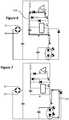
- Figure 8illustrates another embodiment according to the present disclosure.
- the comparator 220is replaced by a PNP switch S4 and a zener diode Z1, which provides the reference voltage Vref.
- the remainder of the circuit in this embodimentis similar to that shown in figure 2 .
- Figure 9illustrates yet another embodiment according to the present disclosure. This embodiment is similar to that shown in figure 8 , with the exception that the connection switch S4 is re re-arranged such that its collector current is conducted by D4, thereby making diode D3 redundant, and reducing the component count relative to that shown in figure 8 .
- Figure 10illustrates a further embodiment according to the present disclosure. This embodiment is similar to that shown in figure 9 , with the exception that blocking diode D5 has been eliminated: as has already been mentioned, and is shown in figure 3 , in order to rapidly discharge the base of S2 in time interval t2-t3, a high current is required. As this current is typically much higher than the base current during time interval t0-t1, D5 can be left out without changing the performance significantly; R4 is relatively high ohmic for the base discharge current.
- R4may be in the range of 100 ⁇ -1kQ, whereas the biasing resistor R1 may be typically be in the range of 100k ⁇ - 1M ⁇ .
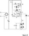
- FIG 11illustrates an embodiment in which this is put into effect.
- a further diode D6is included which blocks current from resistor R1 directly charging capacitor C2; rather it directs the start-up current through R1 to the base of S2.
- This currentis amplified by the current ratio of the bipolar transistor and the capacitor C2 is charged via D4.
- R1can now be chosen to be even more high ohmic - typically in the range 1-10M ⁇ , increasing the efficiency of the SMPS.
- this embodimentprovides for start-up current, and may result in high-efficiency operation than may generally be expected, for instance, from embodiments such as that shown in figure 10 .
- FIG. 12Two examples of such embodiments are shown in figures 12 and 13 .
- the circuit shown in figure 12is similar to that shown in figure 9 , except that S2 is implemented as a MOSFET, rather than a bipolar device.
- the gate charge of S2is used to keep S2 conductive in time interval t1-t2.
- D5For a circuit with a MOSFET it may be appropriate to include D5: without D5 the discharge of the gate charge during t1-t2 might be too high, which could result in that S2 is switched off prematurely.
- FIG. 13illustrates another example not falling within the scope of the claims in which S2 is implemented as a MOSFET.
- start-up resistor R1is reconnected to the gate of S2.
- the gate of S2is pulled up by R1 to the zener reference voltage, (Vref), plus the base-emitter voltage (Vbe(S3)) of S3.
- Vrefzener reference voltage
- Vbe(S3)base-emitter voltage
- start-up S2works as a linear regulator, supplying the capacitor C2 via diode D4. Because S2 is now a MOSFET with a high impedance gate, R1 can be made very high ohmic - 10M ⁇ or more, resulting in a very low dissipation in R1 and a high efficiency.
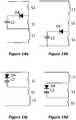
- Figure 14ashows the series arrangement of the power and control switches S2 and S1 and inductor L1, together with the first current path including it diode D4, which charges the capacitor C2 during interval t1 to t2, according to embodiment shown in the previous figures.
- the switches and inductorsmay be arranged differently; for instance as shown in figure 14b , the switches may be on the "low side" of the inductor L1.
- the skilled personwill be aware that most commonly n-type transistors are used for each of the power switch and control switch; however, the present disclosure is not limited to n-type switches.
- embodimentsare not limited to buck converter configurations.
- other embodimentsmay be linked with boost, buck-boost, of flyback configurations.
- the implementation for such other converter typeswill be immediately apparent to the skilled person, and do not require any modifications to the relevant parts of the circuit.
- Embodimentshave been described in which the duration of period t1 - t2 is determined by the time it takes for the voltage on the capacitor C2 to reach a threshold voltage.
- Other embodimentsmay include a time-limiting circuit, which limits the duration of the t1 - t2 interval in the event that C2 does not charge quickly enough - for instance due to a temporary heavy load in the controller. Such a circuit may force the connection switch S3 (or S4 as the case may be) to close at the end of a predetermined period, in the event that the threshold voltage has not been reached.
Landscapes
- Engineering & Computer Science (AREA)
- Power Engineering (AREA)
- Theoretical Computer Science (AREA)
- General Engineering & Computer Science (AREA)
- Physics & Mathematics (AREA)
- General Physics & Mathematics (AREA)
- Computer Hardware Design (AREA)
- Computing Systems (AREA)
- Dc-Dc Converters (AREA)
Description
- This disclosure relates to switched mode power supplies (SMPS) and to lighting circuit comprising such SMPS.
- In some designs of SMPS, the switching element comprises separate but series-connected power switch and control switches. This is currently most frequently the case, and often may be necessary, in designs in which the power switch is a high-voltage bipolar junction transistor. However it should be mentioned at the outset, that a separate power switch and control switch may also be used in designs in which the power switch is a high-voltage MOSFET. Since separate control and power switches are most commonly used with bipolar junction transistors, designs utilising these two switches are often loosely referred to as emitter switched converters. Relative to high-voltage MOSFETs, high-voltage bipolar devices may be significantly cheaper, but since they suffer the drawback of low voltage amplification, they typically require a large base driver current. Switched mode power supplies are typically operated under the control of a controller, which controls the timing of the switching of the switching element. In the case of emitter switched converters the switching element may switch the control switch, and the power switch is arranged and configured to switch following the operation of the control switch.
- A schematic of a SMPS connected to an
AC mains 120 through rectifier B1 and input smoothing capacitor C1, and driving LEDs is shown infigure 1 . In this case the SMPS is a buck converter. The converter comprises a series arrangement of a control switch S1, a power switch S2, and an inductor L1. In this arrangement, the load, which is shown as a series string of LEDs is connected in series with the inductor L1. As shown, power switch S2 is a bipolar transistor which requires a relatively high base current. In order to provide this base current for the power switch S2, the base terminal of the switch S2 is connected to the smoothed rectified mains input through a resistor R1 and a parallel arrangement of a diode D3 and a resistor R4. The value of resistor R4 is chosen so as to set the required appropriate base current for the power switch S2, and diode D3 is provided so as to ensure that S2 can be switched off quickly. The SMPS comprises acontroller 110 which has asupply terminal 114 andground terminal 112. A capacitor C2 is connected across these terminals to provide a supply voltage Vcc to thecontroller 110. Also shown is a sense resistor R2 which is connected to the controller and used to sense the current through the inductor in order to control the switching. - As soon as Vcc rises above the start-up voltage, the controller starts switching. However, typically a switching mode power supply controller consumes more supply current in switching state than in non-switching state. For example additional supply current is needed to drive the power switch. When the current through R1 is just enough to charge C2 to the start-up voltage level (Vstart), it may not be enough to supply the SMPS during operation. The supply voltage would then drop and could reach a voltage level were the SMPS cannot work properly anymore. Typically an under-voltage-lock-out voltage (Vstop) is therefore implemented that stops the operation of the SMPS. As soon as the SMPS stops operating, the supply current of the controller drops again, and the capacitor is able to recharge to the start-up voltage level, which will then repeat the situation were the SMPS starts and stops.
- To prevent this on and off operation, a take-over supply, comprising diode D2 and resistor R3 is added to provide additional current as soon as the converter starts switching and the LED voltage rises above the Vcc level. Alternatively, for flyback converters, an auxiliary winding on the primary side of the transformer may be included to provide power to the controller, once the SMPS is in operation.
- United States Patent Application publication number
US2010/0309689 A1 discloses a bootstrap circuit for a switch mode power supply, a controller for a switch mode voltage converter, a switch mode flyback converter comprising the bootstrap circuit, a switch mode forward converter comprising the bootstrap circuit, and a method of bootstrapping a switch mode power converter. The bootstrap circuit comprises: a current bleed impedance (Rht1) to bleed current from an input power supply (VH+); circuitry to deliver current from the input power supply (VH+) via the current bleed impedance (Rht1) to the base of a power switch (Q1) such that the power switch (Q1) is operable to amplify the current delivered from the internal power supply; a passive circuit (Dst) to provide the amplified current to a reservoir capacitor (Cdd); and the passive circuit element (Dst) further to substantially block reverse current flow from the supply input (Vdd) to the emitter of the power switch (Q1). - According to a first aspect, there is provided a switched mode power supply according to claim 1. We also disclose a switched mode power supply for converting an input voltage and comprising: a series arrangement of an inductor, a power switch and a control switch for controlling the power switch; a controller configured to control the control switch and having a supply terminal and a ground terminal; a capacitor coupled between the controller ground terminal and supply terminal and for providing power to the controller; a first current path arranged to provide charge to the capacitor only when the control switch is open and the power switch is closed; a connectable second current path arranged to draw current from the control terminal of the power switch thereby opening the power switch, and a connection switch configured to connect the second current path in response to a voltage across the capacitor exceeding a threshold voltage.
- By separating in time the occurrence of opening the control switch, and opening the power switch, charge may be provided to the capacitor, from the input (such as a rectified mains). In embodiments in which the capacitor is used to power the controller, it may be possible to thereby avoid the need for an auxiliary power supply for the controller.
- The power switch is a bipolar junction transistor and the current drawn from the control terminal of the power switch is provided
by a base charge of the transistor in an on-state. In arrangements where the control switch is separated from the power switch, it is most common to use a bipolar transistor since they generally may be less expensive than MOSFETs. The base charge in a bipolar transistor is generally much higher than any charge on the gate of a MOSFET. The switched mode power supply further comprises a further current path through the base of the power switch thereby enabling a start-up of the switched mode power supply.
In one or more embodiments the second current path is a recycling path arranged to draw current from the control terminal of the power switch to charge the capacitor. Particularly in the case that the power switch is a bipolar transistor, the base charge may be relatively high, and thus by recycling this charge to charge the capacitor, it might be possible to achieve a significant increase in efficiency of the circuit. - In one or more embodiments, the switched mode power supply further comprises a current path between the power switch control terminal and a positive terminal of the input voltage, which may be a rectified mains.
- The current path arranged to provide charge to the capacitor when the power switch is closed comprises a diode.
- The switched mode power supply may be a buck converter and be arranged for connection of a load in series with the series arrangement. Alternatively and without limitation, the switched mode power supply may be a boost converter and be arranged for connection of a load in parallel with the control switch and power switch in series. Yet further and again without limitation, the switched mode power supply may be a flyback converter wherein the inductor is a primary winding of a transformer, and the switch mode power supply is arranged for connection of a load to a secondary winding of the transformer.
- According to another aspect there is provided a lighting circuit comprising a switch mode power supply has described above, and the load, wherein the load is a string of LEDs. The input voltage may be smoothed rectified mains supply.
- We also disclose a method of controlling a switched mode power supply comprising a series arrangement of a power switch, a control switch and an inductor, the arrangement being connected across a positive and a negative terminal of an input voltage, such as for example a rectified and smoothed mains; a controller having a supply terminal and a ground terminal; and a capacitor coupled between a ground terminal and a supply terminal of the controller and for providing power to the controller; the method comprising; operating the controller to periodically open and close the control switch; providing charge to the capacitor through a first current path only when the control switch is open and the power switch is closed; and in response to a voltage across the capacitor exceeding a threshold voltage, operating a connection switch to connect a second path thereby drawing current from the control terminal of the power switch thereby opening the power switch.
- These and other aspects of the invention will be apparent from, and elucidated with reference to, the embodiments described hereinafter.
- Embodiments will be described, by way of example only, with reference to the drawings, in which
figure 1 shows a schematic of a lighting circuit of a SMPS connected to an AC mains and driving a lighting circuit;figure 2 illustrates a lighting circuit according to embodiments;figure 3 shows various signals associated with the circuit offigure 2 ;figures 4-7 illustrate the current flow through the circuit offigure 2 during one-and-a-half switching cycles;figure 8-13 illustrate example switched mode power supplys; andfigures 14 and15 illustrate example arrangements of a power switch, control switch, and inductor, and with associated current paths for charging a capacitor.- It should be noted that the Figures are diagrammatic and not drawn to scale. Relative dimensions and proportions of parts of these Figures have been shown exaggerated or reduced in size, for the sake of clarity and convenience in the drawings. The same reference signs are generally used to refer to corresponding or similar features in modified and different embodiments.
Figure 2 shows a switched mode power supply according to embodiments, for converting an input voltage. The SMPS, which may also be referred to as a switched mode power converter, comprises: a series arrangement of an inductor L1, a power switch S2, a control switch S1 for controlling the power switch; acontroller 110 configured to control the control switch and having asupply terminal 112 and aground terminal 114; a capacitor C2 coupled between the controller ground terminal and supply terminal and for providing power to the controller; a firstcurrent path 240 arranged to provide charge to the capacitor only when the control switch is open and the power switch is closed; a connectable secondcurrent path 250 arranged to draw current from the control terminal of the power switch thereby opening the power switch, and a connection switch S3 configured to connect the second current path in the event that, or in response to, a voltage across the capacitor exceeds a threshold voltage.- In the schematic of
figure 2 , the SMPS is shown to be connected to the AC mains through rectifier B1 and input smoothing capacitor C1, and drives a string ofLEDs 230. The converter comprises a series arrangement of a control switch S1, a power switch S2, and an inductor L1 (not necessarily in that order). The string of LEDs comprises the load, and is connected in series with the inductor L1. Thecontroller 110 has supply andground terminals controller 110. Also shown is a sense resistor R2 which is connected to the controller and used to sense the current through the inductor in order to control the switching. Power switch S2 is shown as a bipolar transistor. The skilled person will be familiar that a sense resistor may not be required in embodiments in which other means are used to determine the appropriate switching moment of the control or power switches. To provide base current for the power switch S2 at start-up (which will be considered in more detail below), its base terminal is connected to the smoothed rectified mains input through resistor R1. During normal operation, current is provided to the base through R4. A relatively small amount of current may also be provided through R1 - in a typical example, the base current is more than 10mA, and R4 thus has to be able supply this magnitude of current, whereas the value of R1 may be chosen to be able to supply only 1 mA or less. Discharging of the base charge through R4 when the power switch is open, is prevented by a diode D5; however, when the power switch is closed but the control switch is open, current can flow through D4, which thus is in the first current path, to charge the capacitor C2. The connectable current path, through which the base charge may discharge, is provided through diode D3 which connects the base terminal of the power switch to C2 via a switch S3. The connection status of this second current path is thus determined by the closed/open status of switch S3. Switch S3 may therefore be described as a connection switch. The status of this connection switch may be determined, as shown in these embodiments, by a comparator 220, which compares the voltage at the base of the power switch with a threshold voltage. - The value of R4 is chosen to provide the required level of base current for the power switch S2: For a typical high voltage bipolar transistor the current amplification can typically be as low as 12, so if the peak current through S1,S2, L1 needs to be 144mA, the base current needs to be at least 144mA/12=12mA. So if Vcc=13V, R4 needs to be about:

- D3 provides for fast discharge of the bass charge, in both the known solution, and according to embodiments: a low ohmic return path is needed for quick turn-off and high efficiency. Absent the time-interval t1-t2, after time interval t0-t1 where the base current is 12mA, time interval t2-t3 would immediately follow and the base current would be -144mA. This current would come from the base of S2. This high current cannot flow through R4 as this would require 140mA * 942ohm=132V across R4, so to discharge the base quickly D3 is added for recycling the base charge.
- In operation, when S1 is switched on, S2 is switched on via its emitter. The base current for transistor S2 is supplied via D5 and R4. When S1 is switched off, initially S3 is open and S2 remains in a conductive state due to the base charge of S2. The current through S2 now flows through D4 to the capacitor C2. This recharges the Vcc capacitor C2. The Vcc voltage therefore increases. Also the emitter voltage, shown as Vem, and the base voltage, shown as Vbase, each increase as Vcc increases. As soon as the base voltage reaches the 'Vref voltage for the comparator 220, S3 is closed by the comparator. The base charge is then discharged to capacitor C2 via D3 and S2 switches to the off-state. D3 is shown in the figure to make clear that the current may be only in this direction.
Figure 3 shows various signals associated with the operation of a switched mode power supply as described above with reference tofigure 2 , over one-and-a-half switching cycles. Key moments in the switching cycles are shown at t0 - both switches closed, t1 - control switch S1 opens, t2 - power switch S2 starts to open, and t3 - power switch S3 completely open. t4 represents the start of a new cycle and is thus equivalent to t0. The figure shows, from the top: theconduction status 310 of control switch S1, theconduction status 315 of power switch S2, theconduction status 320 of connection switch S3, the collector current 325 in power switch S2, the base current 330 of power switch S2, the current 335 through control switch S1, the current 340 through diode D4, the current 345 through the inductor L1, thevoltage 350 at the base of S2, and thevoltage Vcc 355 at the capacitor C2.- At moment t0, control switch S1 is switched on by
controller 110. Control switch S1 switches power switch S2 on via the emitter. The current in the switches and inductor L1 increases linearly. Due to the base current and also the controller supply current, the Vcc voltage drops. At moment t1, control switch S1 is switched off. The base (and emitter) voltage of power switch S2 rise until diode D4 starts conducting. The current then flows through diode D4, charging Vcc capacitor C2. The Vcc voltage, emitter voltage and base voltage rise until the base voltage reaches the reference voltage Vref at moment t2. Connection switch S3 is then closed and the base charge of power switch S2 is conducted to the capacitor C2 via connection switch S3 and diode D3. Once the base charge has been removed, shown at t3, power switch S2 is back in the non-conductive state. From t3 to t4 the stored energy in the inductor L1 is released in the LED output and C3. Diode D1 is the freewheeling diode of the converter. - It will be appreciated that the signals shown in
figure 3 correspond to boundary mode conduction. That is to say, as soon as the inductor current 345 falls to 0, a new primary stroke starts. However, embodiments may also use either continuous conduction mode or discontinuous conduction mode. In continuous conduction mode, the inductor current does not return to zero, but the subsequent primary stroke starts earlier. This is shown at 390 in the upper cutaway section offigure 3 . In discontinuous conduction mode, the inductor current returns to 0, and there is a subsequent gap before the next subsequent primary stroke commences. This gap is shown at 395 in the lower cutaway infigure 3 . Figures 4-7 show the current flow through the circuit depicted infigure 2 , at various times during the switching cycle:Figure 4 shows the current flow as dashedline 410 through the control and power switches S1 and S2 during interval t0-t1.- The arrangement according to embodiments enables charging of the capacitor C2 thereby providing power to the controller, during normal operation. This occurs during the period t1-2 shown in
figure 3 . This current flow is shown as dashedline 510 infigure 5 . This is without the requirement for a separate auxiliary power supply (such as R3 and D2 shown infigure 1 ). It therefore may be possible to avoid the complexity and expense of a separate auxiliary power supply for the controller. In embodiments in which S2 is fully conductive in time interval t1-t2, this supply may be very efficient. It should be noted that this effect is not the same as a linear regulator: in particular, S2 does not operate in linear mode - which is the case for a linear regulator supplying an SMPS. - The supply voltage Vcc is regulated according to the 'Vref' voltage: that is to say, as soon as Vcc exceeds V(ref), less the sum of the forward voltage U(D4) across D4 and the base-emitted voltage (Vbe(S2)) of S2, S2 is switched off. If a larger load is present on node Vcc, S3 will be kept non-conductive for a longer time after moment t1. The time interval t1-t2 will then be extended. Also when the load on the Vcc node is small, the time interval t1-t2 will be small. Thus the arrangement operates in a self-regulating manner.
- The stored base charge, during period t1 - t2, enables the power switch S2 to remain closed during that time interval. Some embodiments also allow for recycling of this base charge as described above with reference to
figure 2 . This occurs during period t2-t3 shown infigure 3 , and is depicted as dashedline 610 infigure 6 As shown infigure 2 , this is done by connecting the connectable current path, in particular the blocking diode D3, to capacitor C2, to make use of the base charge. It will be apparent to the skilled person that that the diode D3 may be connected to any other suitable point in the circuit. However, it will be appreciated that the current coming out of the base during t2-t3 is very large. The peak base current will be as high as the collector current in that time interval. Recycling the base charge by discharging it to Vcc instead of discharging it to ground, thus may provide a significant increase in efficiency. - Finally, during period t3-t4, the switches S1 and S2 are both open, corresponding to the secondary stroke. Current is then delivered to the load through the fly-wheeling diode D1.
- As will be discussed in more detail hereinbelow, in some embodiment a diode D3 may not be required, since the switch S3 is closed only at times when there is no risk of current flow in the "wrong" direction.
Figure 8 illustrates another embodiment according to the present disclosure. In this embodiment, the comparator 220 is replaced by a PNP switch S4 and a zener diode Z1, which provides the reference voltage Vref. The remainder of the circuit in this embodiment is similar to that shown infigure 2 .Figure 9 illustrates yet another embodiment according to the present disclosure. This embodiment is similar to that shown infigure 8 , with the exception that the connection switch S4 is re re-arranged such that its collector current is conducted by D4, thereby making diode D3 redundant, and reducing the component count relative to that shown infigure 8 .Figure 10 illustrates a further embodiment according to the present disclosure. This embodiment is similar to that shown infigure 9 , with the exception that blocking diode D5 has been eliminated: as has already been mentioned, and is shown infigure 3 , in order to rapidly discharge the base of S2 in time interval t2-t3, a high current is required. As this current is typically much higher than the base current during time interval t0-t1, D5 can be left out without changing the performance significantly; R4 is relatively high ohmic for the base discharge current. For example, R4 may be in the range of 100Ω -1kQ, whereas the biasing resistor R1 may be typically be in the range of 100kΩ - 1MΩ.- In the embodiment illustrated in
figure 10 a small base discharge current will flow in time interval t1-t2. Because the current required to discharge the base is much higher, this current will hardly affect the performance, whereas it lowers the component count even further. - In embodiments in which the power switch is a bipolar junction transistor, this can be used to provide the power for start-up:
figure 11 illustrates an embodiment in which this is put into effect. In this embodiment a further diode D6 is included which blocks current from resistor R1 directly charging capacitor C2; rather it directs the start-up current through R1 to the base of S2. This current is amplified by the current ratio of the bipolar transistor and the capacitor C2 is charged via D4. R1 can now be chosen to be even more high ohmic - typically in the range 1-10MΩ, increasing the efficiency of the SMPS. During normal operation, in time interval t0-t1 D6 is conductive to provide S2 with base current coming from C2, while during time interval t1-t2 (and all other time intervals) D6 blocks the base discharge current. Thus, in exchange for a higher component count, this embodiment provides for start-up current, and may result in high-efficiency operation than may generally be expected, for instance, from embodiments such as that shown infigure 10 . - As has already been mentioned, we also disclose a MOSFET rather than a bipolar transistor for the power switch S2 that does not fall within the scope of the claims. Two examples of such embodiments are shown in
figures 12 and13 . The circuit shown infigure 12 is similar to that shown infigure 9 , except that S2 is implemented as a MOSFET, rather than a bipolar device. Now the gate charge of S2 is used to keep S2 conductive in time interval t1-t2. For a circuit with a MOSFET it may be appropriate to include D5: without D5 the discharge of the gate charge during t1-t2 might be too high, which could result in that S2 is switched off prematurely. Figure 13 illustrates another example not falling within the scope of the claims in which S2 is implemented as a MOSFET. In this example, start-up resistor R1 is reconnected to the gate of S2. In this embodiment, during start-up the gate of S2 is pulled up by R1 to the zener reference voltage, (Vref), plus the base-emitter voltage (Vbe(S3)) of S3. During start-up S2 works as a linear regulator, supplying the capacitor C2 via diode D4. Because S2 is now a MOSFET with a high impedance gate, R1 can be made very high ohmic - 10MΩ or more, resulting in a very low dissipation in R1 and a high efficiency.Figure 14a shows the series arrangement of the power and control switches S2 and S1 and inductor L1, together with the first current path including it diode D4, which charges the capacitor C2 during interval t1 to t2, according to embodiment shown in the previous figures. However, in other embodiments of the switches and inductors may be arranged differently; for instance as shown infigure 14b , the switches may be on the "low side" of the inductor L1. The skilled person will be aware that most commonly n-type transistors are used for each of the power switch and control switch; however, the present disclosure is not limited to n-type switches. Arrangements for the first current path, in the case that the switches are p-type transistors corresponding to those infigure 14a and figure 14b , for high side switching and low side switching respectively, are shown infigures 14c and figure 14d . In each case the capacitor C2 is charged through diode D4 during the time period when control switch S1 is open but power switch S2 is closed.- Finally, it will be appreciated that the ordering of the components of the series arrangement of inductor, control switch and power switch may be different to those shown in
figure 14 . Although the arrangements offigure 14 are generally considered to be the most efficient layout of the series arrangements, others are possible and not excluded, for example the inductor may be between the two switches. Although not covered by the claims of the present invention, some of these arrangements, and the corresponding first current paths to charge the capacitor C2, are shown infigure 15 . - Whereas the embodiments described above have been illustrated with reference to a lighting circuit, and a string of LEDs in particular, it will be appreciated that the present disclosure is not limited thereto, and other embodiments may be associated with may comprise other forms of lighting, such as OLED or electroluminescent, or other loads which are not associated with lighting at all, but maybe without limitation motors, actuators, sensors, heating elements or other electrical loads.
- Furthermore, embodiments are not limited to buck converter configurations. Illustratively, other embodiments may be linked with boost, buck-boost, of flyback configurations. The implementation for such other converter types will be immediately apparent to the skilled person, and do not require any modifications to the relevant parts of the circuit.
- Embodiments have been described in which the duration of period t1 - t2 is determined by the time it takes for the voltage on the capacitor C2 to reach a threshold voltage. Other embodiments may include a time-limiting circuit, which limits the duration of the t1 - t2 interval in the event that C2 does not charge quickly enough - for instance due to a temporary heavy load in the controller. Such a circuit may force the connection switch S3 (or S4 as the case may be) to close at the end of a predetermined period, in the event that the threshold voltage has not been reached.

Claims (7)
- A switched mode power supply for converting an input voltage into a DC output voltage and comprising:an inductor (L1) arranged in series with a series arrangement of a power switch (S2), comprising a bipolar junction transistor, and a control switch (S1), the control switch connected to an emitter terminal of the power switch for controlling the power switch, the inductor (L1) arranged for connection to a load;a controller (110) configured to control the control switch and having a supply terminal (112) and a ground terminal (114);a capacitor (C2) coupled between the controller ground terminal and supply terminal and for providing power to the controller;a first current path between the emitter terminal of the power switch (S2) and the supply terminal of the capacitor (240), the first current path comprising a diode (D4) and arranged to provide a base charge of the bipolar junction transistor to the capacitor, said charge being provided by the first current path only when the control switch is open and the power switch is closed;a connectable second current path (250) between the control, base terminal of the power switch and the supply terminal of the capacitor, and arranged to draw current from the control terminal of the power switch thereby opening the power switch wherein the current drawn from the control terminal of the power switch is provided by a base charge of the bipolar junction transistor in an on-state,and a connection switch (S3) configured to connect the second current path in response to a voltage across the capacitor exceeding a threshold voltage;a further current path from the supply terminal of the capacitor to the central base terminal of the power switch and including a resistor (R4);and whereinthe controller is configured to open and close the control switch, wherein closing of the control switch is configured to close the power switch via the emitter terminal and thereby cause the current in the control switch, the power switch and inductor to rise, wherein the further current path is arranged to provide current to the base terminal at start-up and wherein opening of the control switch provides the base charge to the capacitor through the first current path, when the diode (D4) starts conducting, causing the voltage across the capacitor to rise and wherein when the voltage exceeds the threshold voltage, the connection switch is closed and the base charge is conducted to the capacitor by the second current path thereby discharging the base terminal and opening the power switch.
- A switched mode power supply according to claim 1, wherein the second current path is a recycling path arranged to draw current from the control terminal of the power switch to charge the capacitor.
- A switched mode power supply according to any previous claim, being a buck converter and arranged for connection of a load in series with the series arrangement.
- A switched mode power supply according to claims 1 or 2, being a boost converter and arranged for connection of a load in parallel with the control switch and power switch in series.
- A switched mode power supply according to claims 1 or 2, being a flyback converter wherein the inductor is a primary winding of a transformer, and arranged for connection of a load to a secondary winding of the transformer.
- A lighting circuit comprising a switched mode power supply according to claim 3 and 5 and the load, wherein the load is a string of LEDs.
- A lighting circuit according to claim 6, wherein the input voltage is a rectified and smoothed mains voltage.
Priority Applications (3)
| Application Number | Priority Date | Filing Date | Title |
|---|---|---|---|
| EP14177479.4AEP2975767B1 (en) | 2014-07-17 | 2014-07-17 | A switched mode power supply and lighting circuit |
| US14/728,929US9471138B2 (en) | 2014-07-17 | 2015-06-02 | Switched mode power supply, a controller therefor, a lighting circuit and a control method |
| CN201510418990.5ACN105305847B (en) | 2014-07-17 | 2015-07-16 | Switched-mode power supply and its controller, illuminating circuit and control method |
Applications Claiming Priority (1)
| Application Number | Priority Date | Filing Date | Title |
|---|---|---|---|
| EP14177479.4AEP2975767B1 (en) | 2014-07-17 | 2014-07-17 | A switched mode power supply and lighting circuit |
Publications (2)
| Publication Number | Publication Date |
|---|---|
| EP2975767A1 EP2975767A1 (en) | 2016-01-20 |
| EP2975767B1true EP2975767B1 (en) | 2020-01-22 |
Family
ID=51211088
Family Applications (1)
| Application Number | Title | Priority Date | Filing Date |
|---|---|---|---|
| EP14177479.4AActiveEP2975767B1 (en) | 2014-07-17 | 2014-07-17 | A switched mode power supply and lighting circuit |
Country Status (3)
| Country | Link |
|---|---|
| US (1) | US9471138B2 (en) |
| EP (1) | EP2975767B1 (en) |
| CN (1) | CN105305847B (en) |
Families Citing this family (5)
| Publication number | Priority date | Publication date | Assignee | Title |
|---|---|---|---|---|
| US9788369B2 (en)* | 2014-07-28 | 2017-10-10 | Silergy Semiconductor Technology (Hangzhou) Ltd | LED driver and LED driving method |
| WO2017009979A1 (en)* | 2015-07-15 | 2017-01-19 | 三菱電機株式会社 | Control circuit |
| US10075063B2 (en)* | 2017-01-13 | 2018-09-11 | Dialog Semiconductor Inc. | Dual stage Vcc charging for switched mode power supply |
| US11983063B2 (en)* | 2022-08-31 | 2024-05-14 | Apple Inc. | Scalable power delivery system |
| US12368437B2 (en) | 2023-09-06 | 2025-07-22 | Texas Instruments Incorporated | High voltage converter power stage |
Family Cites Families (13)
| Publication number | Priority date | Publication date | Assignee | Title |
|---|---|---|---|---|
| US20060132111A1 (en)* | 2004-08-02 | 2006-06-22 | Jacobs James K | Power supply with multiple modes of operation |
| US20110199796A1 (en) | 2008-08-28 | 2011-08-18 | Xin Wu | Structure of a power supply |
| US8487546B2 (en)* | 2008-08-29 | 2013-07-16 | Cirrus Logic, Inc. | LED lighting system with accurate current control |
| US20100309689A1 (en)* | 2009-06-03 | 2010-12-09 | David Coulson | Bootstrap Circuitry |
| CN201898641U (en)* | 2010-05-14 | 2011-07-13 | 皇家飞利浦电子股份有限公司 | Self-adaption circuits |
| IT1403159B1 (en)* | 2010-12-02 | 2013-10-04 | Osram Spa | CONVERTER DEVICE. |
| US8674605B2 (en)* | 2011-05-12 | 2014-03-18 | Osram Sylvania Inc. | Driver circuit for reduced form factor solid state light source lamp |
| JP6235464B2 (en)* | 2011-06-10 | 2017-11-22 | フィリップス ライティング ホールディング ビー ヴィ | Driving device and driving method for driving load, especially LED unit |
| US9351354B2 (en)* | 2011-06-17 | 2016-05-24 | Koninklijke Philips N.V. | Driver device for driving an LED unit |
| CN102280995A (en) | 2011-08-29 | 2011-12-14 | 上海新进半导体制造有限公司 | Switch power supply integrated circuit |
| US9461546B2 (en)* | 2013-02-08 | 2016-10-04 | Advanced Charging Technologies, LLC | Power device and method for delivering power to electronic devices |
| EP2787639A1 (en) | 2013-04-04 | 2014-10-08 | Nxp B.V. | Cascode bipolar transistor circuit |
| US9231472B2 (en)* | 2014-04-11 | 2016-01-05 | Infineon Technologies Austria Ag | System and method for a switched-mode power supply |
- 2014
- 2014-07-17EPEP14177479.4Apatent/EP2975767B1/enactiveActive
- 2015
- 2015-06-02USUS14/728,929patent/US9471138B2/enactiveActive
- 2015-07-16CNCN201510418990.5Apatent/CN105305847B/enactiveActive
Non-Patent Citations (1)
| Title |
|---|
| None* |
Also Published As
| Publication number | Publication date |
|---|---|
| CN105305847A (en) | 2016-02-03 |
| US9471138B2 (en) | 2016-10-18 |
| EP2975767A1 (en) | 2016-01-20 |
| CN105305847B (en) | 2018-03-06 |
| US20160018876A1 (en) | 2016-01-21 |
Similar Documents
| Publication | Publication Date | Title |
|---|---|---|
| US8520414B2 (en) | Controller for a power converter | |
| US8488355B2 (en) | Driver for a synchronous rectifier and power converter employing the same | |
| US9590608B2 (en) | Bootstrap refresh control circuit, voltage converter and associated method | |
| EP2975767B1 (en) | A switched mode power supply and lighting circuit | |
| US6504351B2 (en) | Systems and methods for controlling the charge profile during the commutation event of a synchronous switching transistor in a regulator | |
| EP2375554B1 (en) | Lighting device and illumination fixture using the same | |
| US20120112657A1 (en) | Low cost power supply circuit and method | |
| CN103227568A (en) | Flyback converter with primary side voltage sensing and overvoltage protection during low load operation | |
| CN107646165B (en) | LED driver and LED driving method | |
| EP3305023B1 (en) | An led driver circuit, and led arrangement and a driving method | |
| US8611118B2 (en) | Gate drive controller circuit with anti-saturation circuit and power up circuit therefor | |
| CN100502211C (en) | A self-driving circuit of a flyback converter synchronous rectifier | |
| CN109660131B (en) | Switching power supply circuit, power supply method and switching power supply system | |
| CN102035415B (en) | Constant-current implementation method for isolated AC/DC switched power supply for LED illumination drive and special device thereof | |
| Pouladi et al. | Battery operated soft switching resonant buck–boost LED driver with single magnetic element | |
| US11246202B2 (en) | LED lighting driver and drive method | |
| KR102661965B1 (en) | Power supplier and power supply method using the same | |
| US6348818B1 (en) | Voltage-adder LED driver | |
| US20130020958A1 (en) | Led driver operating in boundary condition mode | |
| CN110572046A (en) | DC/DC converter | |
| CN209642550U (en) | A kind of Switching Power Supply power supply circuit and switch power supply system | |
| Hwu et al. | An isolated high step-up converter with continuous input current and LC snubber | |
| JP6994957B2 (en) | Insulation synchronous rectification type DC / DC converter | |
| CN106601193B (en) | Light-emitting diode backlight driving circuit | |
| CN204089624U (en) | Inverse-excitation type switch power-supply |
Legal Events
| Date | Code | Title | Description |
|---|---|---|---|
| PUAI | Public reference made under article 153(3) epc to a published international application that has entered the european phase | Free format text:ORIGINAL CODE: 0009012 | |
| AK | Designated contracting states | Kind code of ref document:A1 Designated state(s):AL AT BE BG CH CY CZ DE DK EE ES FI FR GB GR HR HU IE IS IT LI LT LU LV MC MK MT NL NO PL PT RO RS SE SI SK SM TR | |
| AX | Request for extension of the european patent | Extension state:BA ME | |
| 17P | Request for examination filed | Effective date:20160720 | |
| RBV | Designated contracting states (corrected) | Designated state(s):AL AT BE BG CH CY CZ DE DK EE ES FI FR GB GR HR HU IE IS IT LI LT LU LV MC MK MT NL NO PL PT RO RS SE SI SK SM TR | |
| STAA | Information on the status of an ep patent application or granted ep patent | Free format text:STATUS: EXAMINATION IS IN PROGRESS | |
| 17Q | First examination report despatched | Effective date:20170630 | |
| GRAP | Despatch of communication of intention to grant a patent | Free format text:ORIGINAL CODE: EPIDOSNIGR1 | |
| STAA | Information on the status of an ep patent application or granted ep patent | Free format text:STATUS: GRANT OF PATENT IS INTENDED | |
| INTG | Intention to grant announced | Effective date:20190917 | |
| GRAJ | Information related to disapproval of communication of intention to grant by the applicant or resumption of examination proceedings by the epo deleted | Free format text:ORIGINAL CODE: EPIDOSDIGR1 | |
| STAA | Information on the status of an ep patent application or granted ep patent | Free format text:STATUS: EXAMINATION IS IN PROGRESS | |
| GRAP | Despatch of communication of intention to grant a patent | Free format text:ORIGINAL CODE: EPIDOSNIGR1 | |
| STAA | Information on the status of an ep patent application or granted ep patent | Free format text:STATUS: GRANT OF PATENT IS INTENDED | |
| GRAS | Grant fee paid | Free format text:ORIGINAL CODE: EPIDOSNIGR3 | |
| INTC | Intention to grant announced (deleted) | ||
| GRAA | (expected) grant | Free format text:ORIGINAL CODE: 0009210 | |
| STAA | Information on the status of an ep patent application or granted ep patent | Free format text:STATUS: THE PATENT HAS BEEN GRANTED | |
| INTG | Intention to grant announced | Effective date:20191203 | |
| AK | Designated contracting states | Kind code of ref document:B1 Designated state(s):AL AT BE BG CH CY CZ DE DK EE ES FI FR GB GR HR HU IE IS IT LI LT LU LV MC MK MT NL NO PL PT RO RS SE SI SK SM TR | |
| REG | Reference to a national code | Ref country code:GB Ref legal event code:FG4D | |
| REG | Reference to a national code | Ref country code:CH Ref legal event code:EP | |
| REG | Reference to a national code | Ref country code:AT Ref legal event code:REF Ref document number:1227596 Country of ref document:AT Kind code of ref document:T Effective date:20200215 | |
| REG | Reference to a national code | Ref country code:IE Ref legal event code:FG4D | |
| REG | Reference to a national code | Ref country code:DE Ref legal event code:R096 Ref document number:602014060264 Country of ref document:DE | |
| REG | Reference to a national code | Ref country code:NL Ref legal event code:MP Effective date:20200122 | |
| REG | Reference to a national code | Ref country code:LT Ref legal event code:MG4D | |
| PG25 | Lapsed in a contracting state [announced via postgrant information from national office to epo] | Ref country code:NL Free format text:LAPSE BECAUSE OF FAILURE TO SUBMIT A TRANSLATION OF THE DESCRIPTION OR TO PAY THE FEE WITHIN THE PRESCRIBED TIME-LIMIT Effective date:20200122 Ref country code:FI Free format text:LAPSE BECAUSE OF FAILURE TO SUBMIT A TRANSLATION OF THE DESCRIPTION OR TO PAY THE FEE WITHIN THE PRESCRIBED TIME-LIMIT Effective date:20200122 Ref country code:NO Free format text:LAPSE BECAUSE OF FAILURE TO SUBMIT A TRANSLATION OF THE DESCRIPTION OR TO PAY THE FEE WITHIN THE PRESCRIBED TIME-LIMIT Effective date:20200422 Ref country code:PT Free format text:LAPSE BECAUSE OF FAILURE TO SUBMIT A TRANSLATION OF THE DESCRIPTION OR TO PAY THE FEE WITHIN THE PRESCRIBED TIME-LIMIT Effective date:20200614 Ref country code:RS Free format text:LAPSE BECAUSE OF FAILURE TO SUBMIT A TRANSLATION OF THE DESCRIPTION OR TO PAY THE FEE WITHIN THE PRESCRIBED TIME-LIMIT Effective date:20200122 | |
| PG25 | Lapsed in a contracting state [announced via postgrant information from national office to epo] | Ref country code:HR Free format text:LAPSE BECAUSE OF FAILURE TO SUBMIT A TRANSLATION OF THE DESCRIPTION OR TO PAY THE FEE WITHIN THE PRESCRIBED TIME-LIMIT Effective date:20200122 Ref country code:GR Free format text:LAPSE BECAUSE OF FAILURE TO SUBMIT A TRANSLATION OF THE DESCRIPTION OR TO PAY THE FEE WITHIN THE PRESCRIBED TIME-LIMIT Effective date:20200423 Ref country code:IS Free format text:LAPSE BECAUSE OF FAILURE TO SUBMIT A TRANSLATION OF THE DESCRIPTION OR TO PAY THE FEE WITHIN THE PRESCRIBED TIME-LIMIT Effective date:20200522 Ref country code:SE Free format text:LAPSE BECAUSE OF FAILURE TO SUBMIT A TRANSLATION OF THE DESCRIPTION OR TO PAY THE FEE WITHIN THE PRESCRIBED TIME-LIMIT Effective date:20200122 Ref country code:LV Free format text:LAPSE BECAUSE OF FAILURE TO SUBMIT A TRANSLATION OF THE DESCRIPTION OR TO PAY THE FEE WITHIN THE PRESCRIBED TIME-LIMIT Effective date:20200122 Ref country code:BG Free format text:LAPSE BECAUSE OF FAILURE TO SUBMIT A TRANSLATION OF THE DESCRIPTION OR TO PAY THE FEE WITHIN THE PRESCRIBED TIME-LIMIT Effective date:20200422 | |
| REG | Reference to a national code | Ref country code:DE Ref legal event code:R097 Ref document number:602014060264 Country of ref document:DE | |
| PG25 | Lapsed in a contracting state [announced via postgrant information from national office to epo] | Ref country code:EE Free format text:LAPSE BECAUSE OF FAILURE TO SUBMIT A TRANSLATION OF THE DESCRIPTION OR TO PAY THE FEE WITHIN THE PRESCRIBED TIME-LIMIT Effective date:20200122 Ref country code:SM Free format text:LAPSE BECAUSE OF FAILURE TO SUBMIT A TRANSLATION OF THE DESCRIPTION OR TO PAY THE FEE WITHIN THE PRESCRIBED TIME-LIMIT Effective date:20200122 Ref country code:LT Free format text:LAPSE BECAUSE OF FAILURE TO SUBMIT A TRANSLATION OF THE DESCRIPTION OR TO PAY THE FEE WITHIN THE PRESCRIBED TIME-LIMIT Effective date:20200122 Ref country code:DK Free format text:LAPSE BECAUSE OF FAILURE TO SUBMIT A TRANSLATION OF THE DESCRIPTION OR TO PAY THE FEE WITHIN THE PRESCRIBED TIME-LIMIT Effective date:20200122 Ref country code:RO Free format text:LAPSE BECAUSE OF FAILURE TO SUBMIT A TRANSLATION OF THE DESCRIPTION OR TO PAY THE FEE WITHIN THE PRESCRIBED TIME-LIMIT Effective date:20200122 Ref country code:CZ Free format text:LAPSE BECAUSE OF FAILURE TO SUBMIT A TRANSLATION OF THE DESCRIPTION OR TO PAY THE FEE WITHIN THE PRESCRIBED TIME-LIMIT Effective date:20200122 Ref country code:ES Free format text:LAPSE BECAUSE OF FAILURE TO SUBMIT A TRANSLATION OF THE DESCRIPTION OR TO PAY THE FEE WITHIN THE PRESCRIBED TIME-LIMIT Effective date:20200122 Ref country code:SK Free format text:LAPSE BECAUSE OF FAILURE TO SUBMIT A TRANSLATION OF THE DESCRIPTION OR TO PAY THE FEE WITHIN THE PRESCRIBED TIME-LIMIT Effective date:20200122 | |
| REG | Reference to a national code | Ref country code:AT Ref legal event code:MK05 Ref document number:1227596 Country of ref document:AT Kind code of ref document:T Effective date:20200122 | |
| PLBE | No opposition filed within time limit | Free format text:ORIGINAL CODE: 0009261 | |
| STAA | Information on the status of an ep patent application or granted ep patent | Free format text:STATUS: NO OPPOSITION FILED WITHIN TIME LIMIT | |
| 26N | No opposition filed | Effective date:20201023 | |
| PG25 | Lapsed in a contracting state [announced via postgrant information from national office to epo] | Ref country code:IT Free format text:LAPSE BECAUSE OF FAILURE TO SUBMIT A TRANSLATION OF THE DESCRIPTION OR TO PAY THE FEE WITHIN THE PRESCRIBED TIME-LIMIT Effective date:20200122 Ref country code:AT Free format text:LAPSE BECAUSE OF FAILURE TO SUBMIT A TRANSLATION OF THE DESCRIPTION OR TO PAY THE FEE WITHIN THE PRESCRIBED TIME-LIMIT Effective date:20200122 | |
| PG25 | Lapsed in a contracting state [announced via postgrant information from national office to epo] | Ref country code:SI Free format text:LAPSE BECAUSE OF FAILURE TO SUBMIT A TRANSLATION OF THE DESCRIPTION OR TO PAY THE FEE WITHIN THE PRESCRIBED TIME-LIMIT Effective date:20200122 Ref country code:MC Free format text:LAPSE BECAUSE OF FAILURE TO SUBMIT A TRANSLATION OF THE DESCRIPTION OR TO PAY THE FEE WITHIN THE PRESCRIBED TIME-LIMIT Effective date:20200122 Ref country code:PL Free format text:LAPSE BECAUSE OF FAILURE TO SUBMIT A TRANSLATION OF THE DESCRIPTION OR TO PAY THE FEE WITHIN THE PRESCRIBED TIME-LIMIT Effective date:20200122 | |
| REG | Reference to a national code | Ref country code:CH Ref legal event code:PL | |
| GBPC | Gb: european patent ceased through non-payment of renewal fee | Effective date:20200717 | |
| REG | Reference to a national code | Ref country code:BE Ref legal event code:MM Effective date:20200731 | |
| PG25 | Lapsed in a contracting state [announced via postgrant information from national office to epo] | Ref country code:LU Free format text:LAPSE BECAUSE OF NON-PAYMENT OF DUE FEES Effective date:20200717 Ref country code:LI Free format text:LAPSE BECAUSE OF NON-PAYMENT OF DUE FEES Effective date:20200731 Ref country code:GB Free format text:LAPSE BECAUSE OF NON-PAYMENT OF DUE FEES Effective date:20200717 Ref country code:CH Free format text:LAPSE BECAUSE OF NON-PAYMENT OF DUE FEES Effective date:20200731 | |
| PG25 | Lapsed in a contracting state [announced via postgrant information from national office to epo] | Ref country code:BE Free format text:LAPSE BECAUSE OF NON-PAYMENT OF DUE FEES Effective date:20200731 | |
| PG25 | Lapsed in a contracting state [announced via postgrant information from national office to epo] | Ref country code:IE Free format text:LAPSE BECAUSE OF NON-PAYMENT OF DUE FEES Effective date:20200717 | |
| PG25 | Lapsed in a contracting state [announced via postgrant information from national office to epo] | Ref country code:TR Free format text:LAPSE BECAUSE OF FAILURE TO SUBMIT A TRANSLATION OF THE DESCRIPTION OR TO PAY THE FEE WITHIN THE PRESCRIBED TIME-LIMIT Effective date:20200122 Ref country code:MT Free format text:LAPSE BECAUSE OF FAILURE TO SUBMIT A TRANSLATION OF THE DESCRIPTION OR TO PAY THE FEE WITHIN THE PRESCRIBED TIME-LIMIT Effective date:20200122 Ref country code:CY Free format text:LAPSE BECAUSE OF FAILURE TO SUBMIT A TRANSLATION OF THE DESCRIPTION OR TO PAY THE FEE WITHIN THE PRESCRIBED TIME-LIMIT Effective date:20200122 | |
| PG25 | Lapsed in a contracting state [announced via postgrant information from national office to epo] | Ref country code:MK Free format text:LAPSE BECAUSE OF FAILURE TO SUBMIT A TRANSLATION OF THE DESCRIPTION OR TO PAY THE FEE WITHIN THE PRESCRIBED TIME-LIMIT Effective date:20200122 Ref country code:AL Free format text:LAPSE BECAUSE OF FAILURE TO SUBMIT A TRANSLATION OF THE DESCRIPTION OR TO PAY THE FEE WITHIN THE PRESCRIBED TIME-LIMIT Effective date:20200122 | |
| P01 | Opt-out of the competence of the unified patent court (upc) registered | Effective date:20230725 | |
| PGFP | Annual fee paid to national office [announced via postgrant information from national office to epo] | Ref country code:DE Payment date:20240619 Year of fee payment:11 | |
| PGFP | Annual fee paid to national office [announced via postgrant information from national office to epo] | Ref country code:FR Payment date:20250620 Year of fee payment:12 |