EP2974000B1 - Frequency selective logarithmic amplifier with intrinsic frequency demodulation capability - Google Patents
Frequency selective logarithmic amplifier with intrinsic frequency demodulation capabilityDownload PDFInfo
- Publication number
- EP2974000B1 EP2974000B1EP14764728.3AEP14764728AEP2974000B1EP 2974000 B1EP2974000 B1EP 2974000B1EP 14764728 AEP14764728 AEP 14764728AEP 2974000 B1EP2974000 B1EP 2974000B1
- Authority
- EP
- European Patent Office
- Prior art keywords
- frequency
- signal
- circuit
- digital
- lda
- Prior art date
- Legal status (The legal status is an assumption and is not a legal conclusion. Google has not performed a legal analysis and makes no representation as to the accuracy of the status listed.)
- Active
Links
Images


Classifications
- H—ELECTRICITY
- H04—ELECTRIC COMMUNICATION TECHNIQUE
- H04W—WIRELESS COMMUNICATION NETWORKS
- H04W52/00—Power management, e.g. Transmission Power Control [TPC] or power classes
- H04W52/04—Transmission power control [TPC]
- H04W52/52—Transmission power control [TPC] using AGC [Automatic Gain Control] circuits or amplifiers
- H—ELECTRICITY
- H03—ELECTRONIC CIRCUITRY
- H03D—DEMODULATION OR TRANSFERENCE OF MODULATION FROM ONE CARRIER TO ANOTHER
- H03D7/00—Transference of modulation from one carrier to another, e.g. frequency-changing
- H03D7/14—Balanced arrangements
- G—PHYSICS
- G06—COMPUTING OR CALCULATING; COUNTING
- G06G—ANALOGUE COMPUTERS
- G06G7/00—Devices in which the computing operation is performed by varying electric or magnetic quantities
- G06G7/12—Arrangements for performing computing operations, e.g. operational amplifiers
- G06G7/24—Arrangements for performing computing operations, e.g. operational amplifiers for evaluating logarithmic or exponential functions, e.g. hyperbolic functions
- H—ELECTRICITY
- H03—ELECTRONIC CIRCUITRY
- H03D—DEMODULATION OR TRANSFERENCE OF MODULATION FROM ONE CARRIER TO ANOTHER
- H03D1/00—Demodulation of amplitude-modulated oscillations
- H03D1/14—Demodulation of amplitude-modulated oscillations by means of non-linear elements having more than two poles
- H03D1/18—Demodulation of amplitude-modulated oscillations by means of non-linear elements having more than two poles of semiconductor devices
- H—ELECTRICITY
- H03—ELECTRONIC CIRCUITRY
- H03D—DEMODULATION OR TRANSFERENCE OF MODULATION FROM ONE CARRIER TO ANOTHER
- H03D11/00—Super-regenerative demodulator circuits
- H03D11/02—Super-regenerative demodulator circuits for amplitude-modulated oscillations
- H03D11/04—Super-regenerative demodulator circuits for amplitude-modulated oscillations by means of semiconductor devices having more than two electrodes
- H—ELECTRICITY
- H03—ELECTRONIC CIRCUITRY
- H03D—DEMODULATION OR TRANSFERENCE OF MODULATION FROM ONE CARRIER TO ANOTHER
- H03D11/00—Super-regenerative demodulator circuits
- H03D11/06—Super-regenerative demodulator circuits for angle-modulated oscillations
- H03D11/08—Super-regenerative demodulator circuits for angle-modulated oscillations by means of semiconductor devices having more than two electrodes
- H—ELECTRICITY
- H03—ELECTRONIC CIRCUITRY
- H03D—DEMODULATION OR TRANSFERENCE OF MODULATION FROM ONE CARRIER TO ANOTHER
- H03D3/00—Demodulation of angle-, frequency- or phase- modulated oscillations
- H—ELECTRICITY
- H03—ELECTRONIC CIRCUITRY
- H03G—CONTROL OF AMPLIFICATION
- H03G7/00—Volume compression or expansion in amplifiers
- H03G7/001—Volume compression or expansion in amplifiers without controlling loop
- H—ELECTRICITY
- H04—ELECTRIC COMMUNICATION TECHNIQUE
- H04B—TRANSMISSION
- H04B1/00—Details of transmission systems, not covered by a single one of groups H04B3/00 - H04B13/00; Details of transmission systems not characterised by the medium used for transmission
- H04B1/06—Receivers
- H04B1/16—Circuits
- H04B1/26—Circuits for superheterodyne receivers
- H04B1/28—Circuits for superheterodyne receivers the receiver comprising at least one semiconductor device having three or more electrodes
- H—ELECTRICITY
- H04—ELECTRIC COMMUNICATION TECHNIQUE
- H04L—TRANSMISSION OF DIGITAL INFORMATION, e.g. TELEGRAPHIC COMMUNICATION
- H04L27/00—Modulated-carrier systems
- H04L27/10—Frequency-modulated carrier systems, i.e. using frequency-shift keying
- H04L27/14—Demodulator circuits; Receiver circuits
- H—ELECTRICITY
- H04—ELECTRIC COMMUNICATION TECHNIQUE
- H04L—TRANSMISSION OF DIGITAL INFORMATION, e.g. TELEGRAPHIC COMMUNICATION
- H04L7/00—Arrangements for synchronising receiver with transmitter
- H04L7/02—Speed or phase control by the received code signals, the signals containing no special synchronisation information
- H04L7/033—Speed or phase control by the received code signals, the signals containing no special synchronisation information using the transitions of the received signal to control the phase of the synchronising-signal-generating means, e.g. using a phase-locked loop
- H—ELECTRICITY
- H03—ELECTRONIC CIRCUITRY
- H03D—DEMODULATION OR TRANSFERENCE OF MODULATION FROM ONE CARRIER TO ANOTHER
- H03D2200/00—Indexing scheme relating to details of demodulation or transference of modulation from one carrier to another covered by H03D
- H03D2200/0041—Functional aspects of demodulators
- H03D2200/006—Signal sampling
Definitions
- the subject matter disclosed hereinrelates to a regenerative selective logarithmic detector amplifier (LDA) with integrated FM demodulation capabilities. It can receive a wired or wireless FM modulated signal and amplify or demodulate it with high sensitivity, high skirt ratio and minimized noise when compared to the prior art. When used in conjunction with other circuits such as a phase lock loop (PLL) or mixer, it can improve interference rejection and frequency selectivity and be locked on a precise channel in frequency and phase.
- PLLphase lock loop
- the LDAproduces intermittent oscillations that are self-quenched when reaching a given threshold. It also embeds the circuitry to perform direct FM discrimination. This plus the fact that the instantaneous regeneration gain is low-medium permit to detect signals of small amplitudes buried in the noise.
- the LDAconverts an analog or digital FM, AM, or FM & AM modulated signal and produces a train of almost constant amplitude and quasi-digital pulses in an intermediate frequency over a wide dynamic range.
- a digital frequency to voltage convertermay be used to convert the pulse frequency in a digital voltage word with simple processing.
- a simple analog VFC or peak detectorcan be used to demodulate the input signal to baseband with audio or video bandwidth.
- Innovation factorsinclude direct FM demodulation, high sensitivity and signal regeneration from noise level, high skirt ratio and quasi digital output data without the need of AFC.
- Regenerative selective logarithmic detector amplifiersdisclosed herein have similarities to super-regenerative receivers (SRO) in term of circuit topology.
- the LDAis a phase sensitive regeneration detector, while the SRO is an amplitude sensitivity regeneration device.
- the LDAhas a self-quenching mechanism with low gain that amplifies the signal from the noise floor over a number of cycles.
- the SROhas external quenching and high gain that makes its electrical behaviors and performances quite different.
- the LDA and DC or baseband log ampsboth provide logarithmic amplification over a wide dynamic range.
- the LDAcan have an intrinsic capability to demodulate analog or digital FM or AM & FM simultaneously. Examples of LDAs can be found in U.S. Patent No. 7,911,235, issued to DockOn AG .
- the SROtypically suffers from poor selectivity and higher output noise when used for narrow band signals. SROs also may drift in temperature when the oscillator is LC based.
- the SRO receiverwas quickly replaced by the super-heterodyne receiver for mainstream radio, because the latter has superior selectivity and sensitivity.
- the SROis simple and low power, and has been used over many decades for remote control systems, short distance telemetry, and wireless security. Selectivity and drift limitations were addressed at the end of the 1980s by the use of SAW devices. In the first decade of the 21st century, articles show a renewed interest in SROs for use in low power receivers up to the GHz, range, and for moderate to high data rate applications.
- Baseband log ampsare based on multiple Gilbert cells, and typically provide a good linearity over a mid to large dynamic range at low to high frequencies.
- Simpler logarithmic amplifierse.g. DC log amps
- a self-quench superregenerative wave-signal receiveris known from GB648920A .
- Logarithmic detectorsare known from US2010/237935A1 .
- Super-regenerative demodulatorsare also known e.g. from US5479442 and JPS56138340 .
- LDALow-power digital filter
- SROstate of the art SROs
- log ampslog amps
- LDAscan have intrinsic ability to demodulate frequency with high skirt ratio, very high sensitivity and noise suppression, very high dynamic range, superior discrimination, and flexible placement in a receiver chain without drawback.
- Table 1compares various LDA, SRO. and amp technologies with their respective pros and cons.
- the LDA technology described hereinconcerns a regenerative logarithmic detector amplifier (LDA) with integrated FM demodulation (FM-LDA) that can receive wired or wireless FM, AM, or FM & AM signals with increased sensitivity, interference rejection, and bandwidth relative to circuits in current use.
- LDAregenerative logarithmic detector amplifier
- FM-LDAintegrated FM demodulation
- the LDAcan also amplify signals while minimizing noise.
- the FM-LDAachieves these goals with integral hardware that improves the signal-to-noise ratio SNR of an AM or FM input signal by restarting its cycle automatically, and without external means, whenever the input signal reaches a specific amplitude over time (threshold).
- the LDA circuitthereby convert amplitude or frequency modulated input to an output stream of low intermediate frequency ("IF') frequency pulses, in which the instantaneous frequency modulates with the input wave (i.e. AM/FM transposed to an IF band).
- IF'intermediate frequency
- This output streamis provided as a quasi-digital frequency-pulsed modulated signal.
- AM modulatedthe conversion is made through an intrinsic logarithmic scale and then output.
- the same frequency-pulsed modulated outputcan also be converted to baseband or demodulated (0Hz to F_max) to a voltage varying with time via the adjunction of an analog frequency to amplitude converter, a peak detector or a digital counter, logic inverter, and digital scaling circuit.
- the innovative FM-LDA circuitcan perform several functions, some simultaneously: Logarithmic amplification, signal regeneration, frequency conversion, noise filtering, interference rejection, and analog/digital amplitude/frequency demodulation. More:
- LDA technologycan be integrated into nearly every electronic system that would benefit from higher sensitivity, higher dynamic range, lower power consumption, better interference rejection, increased bandwidth, better signal to noise ratio SNR, longer range, and/or cleaner amplification.
- Figure Idepicts example input and output signals from an LDA.
- An LDAcan give a low-level input signal 101 within its frequency capture bandwidth, masked by white Gaussian input noise 102.
- the LDAcan regenerate an amplified input signal 103 over a number of periods, until reaching a threshold level. When the input threshold level is reached, the LDA can generate an output pulse, and restart its cycle.
- Gaussian noiseis random and uncorrelated with the input signal, and as the regenerated amplified input signal 103 increases, the noise can be averaged out and kept to the same value therefore not amplified over a number of periods, as shown by reduces noise 104.
- Figure 2depicts a combination of the input and output signals from Figure 1 .
- the resulting curve 202represents a regenerated and amplified signal with reduced jitter over time.
- This effectis similar to a LASER in which photons are amplified in a cavity at a specific wavelength.
- a standing wavebuilds up energy constructively over time.
- a discharge of higher energyis produced, and the process restarts.
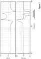
- Figure 3depicts an input with signal and noise 301, a regenerated signal 302, and output frequency pulses 303 at low level.
- Figure 4depicts an input with signal and noise 401, regenerated signal 402, and output frequency pulses 403 at higher input level.
- Figures 3 and 4show a longer time scale of the input, and the effect on output frequency: The input signal (including noise) is shown in at the top, the regenerated signal is shown in the middle, and the output repetition rate is shown at the bottom.
- the LDAtakes time to regenerate the signal and reach a constant threshold value. In the time window of Figure 3 , five regeneration cycles are created.
- Figure 4shows a higher input signal and a corresponding faster regeneration time to reach the threshold.
- the LDAproduces more regeneration cycles in the same time window.
- the output pulsesare almost constant in amplitude for any low-to-high input signals, which is remarkable given the large dynamic range involved.
- the output frequency of the LDAis proportional to the logarithm of the input voltage: or where:
- the output frequencycan be converted into voltage modulation in analog or digital form.
- the output voltage after low pass filteringbecomes or where:
- An LDA with FM demodulation circuitcan possess many intrinsic properties of value to a wide range of commercial technologies.
- the following paragraphsinclude a non-exclusive list of the types of value that may be possible from an LDA with FM demodulation circuit.
- LDAsability to filter random noise from weaker signals gives them the means to extract, for example, a few dBs of signal from the noise floor for smart phone devices or cellular base station receivers.
- LDA technologycan be integrated into mobile phones.
- cellular base stationscould use LDAs to recover weaker signals.
- LDAscan also reduce the power consumption of microprocessors, such as CMOS processors, by integrating the LDAs directly into processing chips.
- the LDAregenerates the input signal and actively reduce noise, the LDA can significantly increase the SNR ratio even if placed after the first or second block in an amplification chain. For instance, a very good sensitivity for FM radio demodulation at 88-108 MHz has been measured when combining an LDA with a low-noise amplifier.
- LDAscan demodulate directly analog/digital AM, FM and other modulations such as FH-SS, and n-ary analog and digital FM and AM modulations with addition of more circuitry such as PLL(s), mixer(s), synthesizer(s), etc.
- LDAscan regenerate many types of low level RF signals if tuned near or at the RF modulating frequency.
- Simplification of wireless digital receiverby replacing several functions of a standard digital receiver (RF to low intermediate frequency or to baseband with direct digital conversion).
- the LDAcan be used as a very low noise and high discrimination conversion gain amplifier with digital output.
- the LDAcan be regarded as a LC circuit with a variable conductance, the latter varying cyclically from positive to negative.
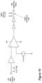
- Figure 5depicts time variant oscillations and quenching cycle of an LDA with FM demodulation capability. More specifically, Figure 5 depicts a cycle 501 from the start of the cycle 502 to the end of the cycle 503. The oscillation builds up 504 until it reaches a threshold level 505 where the oscillation is shunt 506 progressively to zero.
- Figure 6depicts a quadripole 600 with a parallel resonant circuit 601 and a series resonant circuit 602.
- the LDA with FM demodulation capabilityis based on the use of a quadripole made of a parallel and series resonator circuits 601 and 602 as shown in Figure 6 . It is designed to be a bandpass filter with a null phase in the passband.
- An example of parallel resonant circuitis a L an C connected in parallel.
- An example of series resonant circuitis a L an C mounted in series.
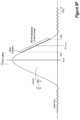
- the transfer function in amplitude and phase of the quadripole of Figure 6is shown in figure 7 .
- Horizontal scaleis frequency in Hz and vertical scales are respectively gain in dB and phase in degree.
- Figure 7depicts a bode plot showing the approximate response of the quadripole.
- the useful operating range for FM/AM demodulationin shown in the ellipse with dashed lines.
- the plots in Figure 7show the amplitude versus the frequency (top) and response phase vs. frequency (bottom).
- the gaincan be designed to be flat or rounded versus pointy with the two spikes as shown in the diagram.
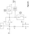
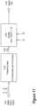
- Figure 8Adepicts a block Diagram of LDA with integral FM demodulation circuit.
- the behavior principleis the following:
- An amplifier A81is made to oscillate with the capacitor C81 in loopback.
- a typical amplifiermay be a NPN, PNP transistor, a FET transistor, A MOS transistor, a dual gate FET transistor, etc.
- the configuration of the active circuitcan be Darlington, common-base, common collector, common emitter, Cascode, differential pair, etc.
- Other types of amplifiersuch as single or multiple stages amplifiers, logic amplifier may be used.
- An amplifiercan be made by any number of processes, such as Silicon, Bi-CMOS, GaAs, or any other process.
- the simplest implementationis to have a 180-degree shift from the input 801 to the output of the amplifier A81 and the oscillation to be maintained with C81 as a weak or strong coupling.
- the value of C81reduces the amplifier gain to a low value as desired.
- the quadripoleis added to the output of A81 and due to its high lower attenuation in the passband makes the amplifier resonate at or around the center frequency.
- the optimal FM demodulation modehappens when the circuit is adjusted to the center of the null phase range and operates there as shown in Figure 7 .
- the maximum frequency deviation that can be demodulated without distortionis equal or larger than the null phase bandwidth, so the bandpass filter quadripole can be designed to accommodate the target deviation, whether narrow or wide.
- R81 and C83acting as a sampling circuit.
- the RC circuit R81 and C83When connected to the amplifier, it charges cyclically and as its potential grows, the voltage across R81 grows that increase the output current of the amplifier. At the same time, the input bias current of the amplifier reduces and at a given threshold switches off the amplifier and therefore the oscillations. At this point, the charge accumulated into C83 discharges in R83 and as a consequence the voltage on R81 and C83 decreases to zero. The cycle restarts and since the potential on R81 and C83 is low the amplifier bias current tends to increase and after a little period of time the oscillation build up again.
- the signal on R81 and C83is the output repetition frequency and its shape may resemble the envelope of the cyclic oscillation frequency shown in Figure 5 .
- the diode D81couples the amplifier to the RC circuit R81 and C83 and acts as a low pas filter with good RF behavior. It has a low impedance when in conduction (positive half cycle of the input voltage) and high impedance when in non-conduction (negative half cycle of the input voltage) acting as a rectifier and low pass filter when loaded with a RC circuit.
- the inputis weakly coupled to the top of diode D1.
- the input matchingis important and a good matching can improve the performance by a significant factor.
- An optional capacitormay be connected between the cathode of D81 and the bias of the amplifier to increase the coupling and facilitate the repetitive cycling.
- the diode D81can be replaced with an inductor of relatively high value e.g. ten times the value of the inductance(s) of the resonator and in a range of 100nH to 1mH. If the LDA oscillation operating frequency is too high, the parasitic may impact adversely the low pass effect and a more ideal component such as a diode may be used.
- D81can be replaced by an active component such as a transistor that is properly biased.
- FM discriminator or demodulatorsThere are several types of FM discriminator or demodulators: Foster-Seeley, Travis, quadrature detector, PLL amongst other.
- the Foster-Seeley discriminatoruses a special center-tapped transformer that is tuned for the frequency of use and two diodes in a full wave rectification. When there is no deviation, both halves of the transformer are equal. When a FM signal is applied, the balance is destroyed and a signal appears at the output that is proportional to the frequency deviation.
- the Travis discriminatoris similar to Forster-Seeley whereas the secondary of the transformer has a center tap and two opposite branches, each branch connected to a tuning circuit and a slope detector.
- First tuning circuitresonates slightly higher than the carrier, while the second one slightly lower.
- the outputis the difference between the voltages of slope detector 1 and 2.
- the inputis split in 2 and one of the paths is delayed by 90 degrees and applied to a resonant LC circuit
- the 2 signalsfinally feed a phase comparator and the result that is low pass filtered is the demodulated FM output.
- the PLLis one FM discriminator and was adopted with the easy access of integrated circuits.
- the phases of the incoming FM signal versus the one of a voltage-controlled oscillator (VCO)are compared.
- the resultis low pass filters and controls the VCO.
- a correction voltageappears at the phase detector that wants to compensate the phase difference by increasing or decreasing the phase and frequency of the VCO. If the loop bandwidth of the PLL is designed appropriately, the correction voltage to the VCO is also the demodulated output voltage.
- the LDA technologies disclosed hereinbring some important novelties.
- An S-curve characteristic outputis provided as other discriminators and the LDA simulates the performance of a Travis discriminator simply by having a low gain amplifier that is only oscillating if the phase of input and output are 180 degree from each of other.
- the S-curveexceeds the quadripole passband bandwidth.
- the FM-LDAdoes not need an automatic frequency control AFC as conventional FM discriminators and it does not need to sit exactly in the center of the S curve. In our implementation there is an auto-centering effect.
- the LDA oscillatorWhen the phase is distorted into the S-curve, the LDA oscillator tries to stay at the center of it. If the deviation goes high in frequency, the repetition rate decreases, if the deviation goes below or lower in frequency, the repetition goes faster. It is similar to having a power meter which can have three readings: close to center channel, center channel or above channel. If the S-curve is very wide, it can demodulate very wide FM. On the other side, if the S-curve is narrow, it can demodulate narrow FM.
- the output repetition frequencycontains the phase and frequency information and is modulated at a low intermediate frequency by the FM input signal.
- Standard FM discriminatorsemploy a constant amplitude. In the LDA technologies disclosed herein, this is provided intrinsically by the LDA that has a large amplitude input dynamic range and that provides an almost constant repetition rate amplitude regardless of the input amplitude large or very small.
- the baseband signalis recovered by an analog or digital frequency to voltage converter (FVC).
- the advantages hereinclude one or more of the following: very high sensitivity over a high dynamic range, constant repetition output amplitude, high skirt ratio (high selectivity), and simultaneous FM & AM demodulation that add a few more dB of amplitude to the baseband demodulation amplitude.
- Figures 8B and 8Cdepict other embodiments of an LDA with integral FM demodulation circuit and an alternate output.
- the embodiments in Figures 8B and 8Cinclude a low pass filter 802 configured to filter signals passing to an alternate output.
- the low pas filter 802filters signals exiting the parallel resonant circuit to the alternate output.
- the low pas filter 802filters signals that enter the parallel and series resonant circuits. Other variations of these embodiments are possible.
- the series resonant circuitmay be removed and the LDA may still demodulate analog or digital FM based on the slope detection method.
- Narrow band or relatively wide band FMmay be demodulated.
- Digital FMincludes modulation such as n-ary FSK, MSK and Gaussian filtered or not Gaussian filtered.
- An example of analog FMis audio FM modulation from 20-20KHz.
- An example of digital FM modulationis 4-GFSK.
- Fig 8Dshows the block diagram of the LDA. This is similar to Fig. 8A , 8B , 8C , 9 , and 14 where the series resonant circuit has been removed. All the other descriptions, functions and methods described in this patent continue to apply for this implementation for instance the analog or digital F!V converter.
- the optimal FM demodulation modehappens when the input RF modulated signal frequency is adjusted to the left or right slope of the frequency Bell shape of the LDA.
- Fig 8Eshows where a narrow band (NB) FM demodulation can be done versus the center of the LDA frequency Bell-shape response. Since the information is carried by the rate of change, little distortion is expected whether the deviation is up in the slope, centered in the slope or low in the slope.
- a preferred implementationis to demodulate on the right slope center where the analog (e.g. audio) or data is not inverted. Oppositely if demodulation is done on the left slope, the analog signal or data will be inverted. It may be un-inverted by negating the signal or multiplying it by -1 further on in the receiver chain.
- Fig. 8Fshows the demodulation of a relatively wideband (WB) FM signal.
- the LDAneeds to exhibit a wider bandwidth and may be designed such as the Q factor of the resonant circuit is lowered and other parameters of the LDA updated. This may include the amplifier AC and DC gain, the bias, the feedback capacitor C81 of figure 8B , amongst other. In consequence the response of the LDA provides more available slope bandwidth to demodulate the wide band FM modulates signal at shown on fig. 8F .
- the discriminated outputis shown following the matching network 803.
- an analog or digital frequency to voltage converterTo complete the FM demodulation output needs to be followed by an analog or digital frequency to voltage converter.
- Three alternate outputsare possible that may have a matching network 804 and a low pass filter 802. These three alternate may provide a higher power level of the demodulated signal and may not require a frequency to voltage converter if the low pass filter cut frequency is lower than the repetition frequency f rep .
- the signalis picked up from the input of the amplifier A81.
- the signalis picked up from the output of the amplifier A81.
- the signalis picked up from a split in the capacitors in the parallel resonant circuit.
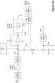
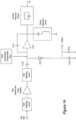
- Figure 9depicts an embodiment of a schematic of an LDA with FM demodulation.
- Figure 9shows an implementation of an LDA with FM demodulation capability.
- the parallel resonator circuit L91/C93 and series resonators circuit L92/C98are found on the collector of the amplifier.
- the amplifiercan be a NPN transistor.
- the transistorproviding a 180 degree phase shift between collector and emitter, C91 the feedback oscillator capacitor, VG91 the input source signal coupled through a capacitor (not shown), the bias VS92, R93, and C96, D92 the diode coupling to the RC circuit R94, C911 and the output VM91.
- An optional C97is shown for improving the quenching process.
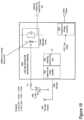
- Figure 10depicts an example of a conversion of a pseudo-digital frequency input 1001 to a digital output pulse stream 1002.
- the repetition frequency rateis quasi-digital and needs little processing to be shaped in to a digital signal.
- the amplitude peak to peakis smaller than around 0.5Vpp, it can be amplified. If as shown the amplitude is 0.1 Vpp, the gain is about 5 to 20. The amplification can be done in one or several steps. Thereafter the amplified signal is compared with a reference voltage V_ref and create a logic "1" when above V_ref and "0" otherwise.
- One or more logic gatescan be added to provide sharp edges and TTL level to the now digital signal.
- the digital repetition frequency output signal 1002can contain the information in phase and instantaneous frequency. As said earlier it can be carried over long distance or in a noisy environment and is noise insensitive since the information is not in amplitude.
- Figure 11depicts conversion of digital pulse stream 1101 to digital equivalent voltage sample 1105.
- the digital repetition frequency signal 1101can be converted into a digital voltage V(k) 1103 by going through an instantaneous frequency meter 1102.
- the digital repetition frequency signal 1101can be passed through a period meter followed by a digital inverse function.
- the digital voltage V(k) 1105is obtained after scaling 1104 as follow:
- FIG 12depicts an example of an analog frequency to voltage converter (FVC).
- the FVCcan be used in conjunction with the FM-LDA. It connects to the repetition frequency output of the LDA. As its name indicates, it provides an output with mean value being the converted voltage. Further low pass filtering may be added.
- Thisis a simple FVC but it has some limitations: the slew rate is slower than the previous digital approach for instance and typically needs a few pulses to settle to an accurate mean voltage value.
- Figure 13depicts one embodiment of an analog detector. Other embodiments are possible.
- the analog detectorcan be connected to the repetition frequency output (VM1), figure 9 or as well at the input of the amplifier, base of T91 of figure 4 . Further low pass filtering and amplification may be added.
- Figure 14depicts another implementation of an LDA.
- the temperature compensated bias 1404 for the amplifier input A141may be designed to temperature compensates the amplifier A141. For instance if the amplifier is made of a bipolar transistor, its VBE will change with -2mV/degree. If the DC bias voltage is made to decrease as well by -2mV/degree, the DC voltage on the emitter will remain constant and therefore the DC current through the resistor R141 as well.
- a temperature compensated current sourcemay be used.
- the amplifierWhen the amplifier is acting as a current amplifier with a constant low frequency gain, the output current will substantially be equal to the bias current multiplied by the gain.
- the amplifier output currentWith a temperature compensated bias current the amplifier output current will also be temperature compensated if we assume that the low frequency gain remain constant with temperature.
- the amplifieris made of a bipolar transistor, and if the DC base current is temperature compensated and constant, the DC collector current will be constant as well.
- the DC emitter currentis the addition of both base and collector currents, that is also constant.
- a constant current across the resistor R141creates a constant DC voltage irrelevant of the variation of the base-emitter voltage.
- the input bias current sourcebeing high impedance will automatically provide a voltage that will change with the base-emitter voltage VBE of - 2mV/degree and compensate it.
- An LDA with FM demodulationmay suffer from some weaknesses such as leak of RF energy from its oscillator throughout the input port. This is an aggravating factor for at least two reasons. First, when the LDA is used as the first stage in a RF receiver, the RF energy is fed backward to the antenna. This causes the antenna to radiate unwanted energy in possibly unintended frequency band(s) and cause EMI noise. Second, the leaking energy can be reflected back to the LDA input with a different phase versus the input signal-a fact that defeats the purpose of regeneration (regeneration is the slow buildup of a resonance phase coherent with the input signal). Therefore it reduces the RF sensitivity.
- the regenerative partcan improve the SNR when placed in first place or at any location in the receive chain. Therefore the regenerative LDA can make good use of a preceding low noise amplifier even in a noise limited amplifier receiver chain.
- Such LDAmay amplify further a signal buried in the noise because the dynamic range is extended on the low side (noise level) of the signal.
- the hypothetic addition of a LNAwould be of little use since the system would be noise limited.
- a matching circuit(s) 1401 at the LDA inputmay improve the coupling with the preceding circuit and reduce the input reflections.
- an isolator 1403 at the input 1402e.g., an amplifier with high factor of isolation
- the LDAcan be regarded as a LC circuit with variable conductance, the later varying cyclically from positive to negative. Consequently the input impedance may vary with time and moves, for example, on an arc in the low right quadrant of the Smith chart in relation with the time variant LDA oscillation cycle.
- Figure 15depicts examples of matching network designed with microstrip lines.
- the series microstripwill change the real part of the impedance and the shunt stub will adjust the imaginary part.
- the shunt stubcan be opened or shorted.
- the shunted stubcan be placed before or after the series microstrip line depending where the normalized load impedance is situated on the Smith chart. If the normalized load impedance is inside the 1+jx circle on the Smith chart then the stub should be placed after and if the normalized load impedance is outside the 1+jx circle on the Smith chart then the shunted stub should be placed before the series microstrip line.
- FIG. 16depicts examples of matching network designed with right-left handed transmission lines (CRLH-TLs).
- Figure 17depicts an example of a solution for matching at two frequencies using the matching network designed with right-left handed transmission lines (CRLH-TLs) shown in Figure 16 .
- CTLH-TLsright-left handed transmission lines
- the CRLH-TL B shown in Figure 17can be opened ended or short-circuited.
- the topology of Figure 17can be slightly modified for similar results.
- the CLAcan be moved to the right of CRA and LLA.
- the topology of Figure 17can be slightly modified for similar results.
- CLBcan moved to the right of CRB and LLB.
- the CRLH-TL Acan be designed to have a frequency f 1 with a phase ⁇ 1 and a frequency f 2 with a phase ⁇ 2 .
- a CRLH-TLcan be designed by using for example a series inductor LRA, a shunt capacitor CRA, a series capacitor CLA and a shunt inductor LLA.
- the CRLH-TL Bcan have, for example, a series inductor LRB, a shunt capacitor CRB, a series capacitor CLB and a shunt inductor LLB.
- the impedances of the CRLH-TL A and CRLH-TL Bcan be defined by:
- the series CRLH-TL Acan define the real part of the impedance and the shunt CRLH-TL B can define the imaginary part. It is also possible to design variable impedances by replacing the fixed components LRA, CRA, LLA, CLA and LRB, CRB, LLB, CLB by variable/tunable capacitors and variable/tunable inductors. Therefore, the impedances can be changed accordingly to the frequency of operation. For example these variable impedances can be inserted at the input and output of the LDA, between the LNA output and the LDA input. A variable matching can be inserted at the output of the repetition frequency. Or in order to have a variable/tunable LDA, it is possible to tune the oscillation frequency to different values by replacing the fixed values of the inductor and the capacitor by variable ones.
- Figure 18depicts one potential implementation of CRLH-TLs.
- the series branch CRLH-TLAis figure 18 is connected to the LDA and a parallel CRLH-TLB is connected to LNA/input and branch left open at the bottom where the topology of Figure 17 was modified such as CLA is moved to the right of CRA (toward LDA).
- FIG 19depicts an example of an LDA 1900 as a high sensitivity FM radio receiver and demodulator.
- the FM-LDAcan be used as RF front end for a FM radio.
- the FM radio channel antenna 1901can feed directly the LDA input 1902.
- An optional LNA 1903 and matching circuit 1904can be used to increase the sensitivity and reduce the leaking though the input port.
- the demodulated audio outputcan be obtained by converting the LDA output repetition rate into a voltage with a FVC 1905 either analog or digitally.
- the FM channelis selected with the DC voltage V_tune 1906 applied to the varicap.
- This configurationgives a wide band FM demodulation output.
- Other configurationsare possible where narrow band FM can be demodulated (e.g., using a PLL implementation, as discussed below).
- Figure 20depicts an example of a varicap circuit implementation for differential- or single-ended tuning voltage with a fixed reference voltage and potentiometer Rpl.
- Figure 20shows a possible implementation of a differential- or single-ended control of the varicap.
- a DC voltage V_tuneis applied on the varicap Cv through high impedance Rv201 and Rv202.
- the total additional capacitance C ADD of the varicap branchis C V series with C201 and C202, as follows:
- C201 and C202should be greater or much greater than Cv.
- the capacitance of C OTHERmay be the combination of all other contributions of capacitance seen at the bottom node of parallel resonance circuit. It may include the contribution of an active component's equivalent capacitance (e.g. transistor C_CE // C_CB), the one of the feedback capacitor C81 of Figure 8 , plus parasitic capacitance due the printed circuit, etc.
- the capacitance of the parallel circuitis removed and replaced by the arm of the varicap.
- the term C RES_PARALis zero in the formulas above.
- the adjustment of frequencyis done manually or mechanically with an adjustable capacitor or inductance.
- the capacitor of the parallel resonance circuitis replaced by an adjustable capacitor that adjusts the frequency radio channel.
- a bunch of fix selectable capacitorsmay be added to extend and cover the entire frequency bandwidth of 88MHz to 108MHz (i.e., a range of frequencies).
- capacitorsmay be chosen for instance to linearize the output frequency versus the input selection since the output frequency is roughly proportional to the inverse square root of the LC product.
- inductancemay be varied instead of or in addition to the capacitors with a sequence that can be binary, decimal or otherwise varied.
- one small-value varicapcan be added to a bank or inventory of fixed selectable capacitors.
- the small-value varicapcan be added to increase the adjustment resolution.
- several varicapscan be used in parallel.
- several capacitors, including at least C 1 , C 2 , and C 3can be placed in parallel.
- One capacitor C 1can have capacitance in a range of about 0.5C to about 1.5C;
- another capacitor C 2can have capacitance in a range of about 1C to about 3C;
- another capacitor C 3can have capacitance in a range of about 2C to about 6C.
- Additional capacitorscan be also be placed in parallel to supplement capacitors C 1 , C 2 , and C 3 .
- a collection of LC circuitcan be switched ON and OFF to change the oscillation frequency of the LDA.
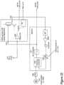
- FIG. 21depicts an LDA-pulsed oscillator 2104 locked in frequency and phase in a phase lock loop (PLL) 2102 to a precise reference frequency tuned to the desired FM radio channel.
- PLLphase lock loop
- the selection of the channelcan be controlled by a digital IC, a processor unit or by the end user with a "digital dialer" such as found in the FM car radios.
- the pulse oscillations of the LDA 2104are filtered, amplified and digitized and feeding a frequency divider by N 2103.
- a phase/frequency comparatorcompares the signal issued from the N divider and a reference signal.
- the reference signalcan be generated from a local oscillator 2101 such as a digital crystal oscillator divided by a counter M 2106.
- the phase/frequency comparator 2107creates a correction voltage proportional to the phase/frequency difference between both input signals.
- Several types of comparatorscan be used with various properties namely gain, output range, output impedance and type of output signal (pulse, variable voltage, etc.).
- a low pass filterfollows, that determines the loop response of the PLL.
- the filtered signal Vc(t)feeds the varicap of the parallel resonant circuit of the LDA 2104 as described previously. Effectively the log amp is used as a controlled VCO.
- the demodulated FM signalis the control voltage Vc(t).
- the loop bandwidth of the PLL 2102can be adjusted appropriately, in this configuration should be lower than the lowest audio frequency of the FM radio channel, say 50Hz.
- the PLL loop bandwidthis affected by the ratio M, the phase comparator gain in rad/s and the VCO gain in MHz/V.
- the comparison frequencymay be of 0.1MHz maximum or any modulo value below such as 50KHz, 25, 20, 10KHz, etc.
- M and Ncan adjusted for getting this value of 0.1MHz at the input of the phase comparator.
- the ratio Ncan be set to 10 ⁇ F_channel in MHz for instance 880 for 88.0MHz, 881 for 88.1 MHz, ..., 1079 for 107.9MHz and 1080 for 108.0MHz.
- An optional squelch function 2108can be added as usually used in FM radio. This can prevent noisy audio content from being passed through when there is no radio channel present.
- the squelch switch 2108may be controlled by the audio demodulated RMS value of the LDA audio output voltage. When the RMS value exceeds a given threshold, it is assumed that the LDA is locked onto a radio channel of sufficient level.
- demodulated audio outputsare possible.
- One possible outputis a narrow band FM (or phase) with the control voltage of the VCO (i.e., Vc(t)).
- Another possible outputis a wide band FM with the regular LDA pulse frequency output that is converted to voltage with a simple frequency-to-voltage converter.
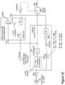
- Figure 22depicts an embodiment of an LDA-based FM radio receiver with digital channel tuning with antenna. This embodiment is similar to the previous one depicted in Figure 21 , with at least the following differences.
- the embodiment depicted in Figure 22can provide very high sensitivity due to its inclusion of an antenna 2210, a LNA 2209 and a regenerative LDA 2204.
- a suitable antennais a roughly omnidirectional small (e.g., 2 square inch) antenna 2210 that can be printed on the same printed circuit board embedding the magnetic H (loop) and electrical field E (monopole/dipole) reception for best coupling and penetration through partition such as a car dashboard.
- a very suitable and preferred printed antenna for this useis a CPL antenna that maximize both the H and E field due to its geometry.
- An LDA based FM radio receiver with the features described hereincan be built for digital radio, satellite radio, and the like. Similar types of topologies can be used for satellite radios and digital radios.
- An LDAcan be used in a FM receiver, an AM receiver, or a combined FM and AM receiver and demodulator.
- One advantage for the LDA receiver with FM demodulationis that it can demodulate FM, AM or both simultaneously. This provides a gain of a few dB versus conventional discriminators.
- Another advantageis the high skirt ration of the LDA that provides superior selectivity. For instance in the case of FM radio, a high skirt ratio can permit better audio quality when listening to a weak signal while a strong one is very close (e.g., it has the ability to discriminate both the strong and the week signal).
- Figure 23depicts a high-sensitivity, low-noise amplifier replacement based on FM-LDA and PLL for FSK or frequency hopping spread spectrum FH-SS modulations. This embodiment can target intrinsic demodulation of digital FM signals and digital FM FH-SS.
- the LDA 2304 in FM modecan demodulate intrinsically the FSK input 2310 modulation with a high sensitivity. Adding the LDA in a PLL 2302 can increase the selectivity with a higher skirt ratio, increase the interference rejection and permit to select precisely the narrow band or wide channel desired. This is a direct demodulation to BB or low IF and there is no super-heterodyne stage here.
- the input noise bandwidthmay cover the entire frequency band (more than the channel BW) or oppositely only one particular channel. However in both cases the regeneration factor may increase the signal-to-noise ratio.
- the outputmay be selected from one of the following and depending of the application:
- a set of selectable parallel and series resonatorscan be added to the LDA.
- the added complexitymay not be a relevant factor anymore.
- the circuitcan be used for amplification and demodulation of one or more frequency modulated signal(s) issued from one or more sensor(s).
- Typical applicationsmay cover sensor such as crystal resonator oscillating at a frequency function of the temperature or other physical parameters.
- the inputmay be wireless or wired.
- Some impedance matching or polarization/bias networkmay be used to interface the one or more sensor(s) and the FM-LDA.
- Other sensorsmay include piezoelectric sensors, accelerometers, even array of sensors. Modulation may include frequency chirping or sweeping.
- a super-heterodyne stagecan be added in the input such as shown in Figures 24A and 24B .
- Figure 24Adepicts an embodiment of a high-sensitivity, low-noise amplifier based on FM-LDA for FSK or FH-SS modulations with super-heterodyne topology.
- Figure 24A and 24Bdepicts an embodiment of a LNA replacement for a FSK receiver 2401 based on FM LDA and super heterodyne reception.
- the advantage of the super heterodyne topologymay be to generate a fix input frequency that permits to apply a high order filter and therefore gaining a high selectivity.
- the following circuits in the receive chainare treating a signal at a fix frequency whatever the channel selected since the variable channel frequency called RF in Fig. 24A , is selected by a variable frequency on LOI such as the mixer output 2402 provides an intermediate frequency IF that is equal to difference of the frequency of RF minus the one of LOI amongst other terms that are generally filtered out.
- LOIis selected by the receiver such as to select one channel amongst N channels in RF frequency and down-convert it in frequency to and intermediate fix frequency IF regardless of the channel selected.
- the LDAbeing intrinsically a narrow band amplifier and regenerative device, it filters-out the frequency components outside of his frequency bandwidth of operation with a high order of filtering. It exhibits the functionality of an active band pass filter with high order of filtering on both the high cutting frequency and low cutting frequency sides.
- One application of the LDAis providing more range, more signal-to-noise ratio, more dynamic range and more interference rejection as a component or sub-system replacement.
- the LDA solutionis integrated in an integrated circuit or a small module such as done currently for VCO modules in the industry, it may be a high performance drop-in replacement for a RF low noise amplifier LNA in a number of FM/FSK/FH-SS receivers. The value would be to increase the performance without completely redesigning the receiver but replacing one component.
- a standard RF LNAcan be replaced by a circuit based on the LDA with FM demodulation.
- a number of advantagescan be derived by making such a replacement, including without limitation:
- This embodimenthas also superior performance versus a classic super-heterodyne receiver, mainly the higher sensitivity, the higher dynamic range, the higher rejection of strong interferences, and the higher selectivity due to the high skirt ratio.
- This embodimentcan be used for FM narrow or wideband modulation, digital FSK or FM based FH-SS.
- local oscillators LO1 and LO2can fixed. If the signal is in a channel in a frequency band (i.e., a range of frequencies), local oscillators LO1 and LO2 can be adjustable. If the input signal is digital FM and frequency hopping spread spectrum, LO1 and LO2 can be agile and change their frequency and follow the input RF signal as it hopes from channel to channel.
- the super-heterodyne structure and high skirt ratio of the LDAprovide a high selectivity and high rejection of interferences. Whereas the LNA can cover the entire frequency band of use, the LDA technologies disclosed herein focus on the selected channel. The performance is therefore superior such as listed above.
- the input signal in figure 24Bis down converted using a mixer 2402 to a fix IF frequency at F_RF - F_LOI .
- the unwanted component at F_RF + F_LO!is filtered out by the LDA 2403 that is frequency selective and designed to match the IF frequency with a given bandwidth f_EF +/- BW.
- the LDA 2403is regenerating the input signal so provides a high sensitivity even after a mixer 2402.
- a LNA 2404can be integral to the LDA 2403 to further improve the sensitivity and increase the isolation to the input port and avoid RF energy to lick out on the input (mixer 2402 and antenna 2401).
- the output frequency repetition of the LDA 2403may be at least 1 to 2 times faster than the highest data input.
- the LDAis not synchronized with the symbol rate of the input data and in order to respect the Nyquist criteria, the output frequency F_rep should be at least twice higher than the highest input data rate.
- the LDAis synchronized with the symbol rate of the input data and in this case the output frequency F_rep may be at least once the highest input data rate because what may really count is the rate of change of F_rep that should be twice or more the one of the input data.
- Finally itis mixed (up converted) back to RF with another mixer 2406 and LO2 at the output RF frequency.
- the output signalcould contain an image at F_RF - 2 ⁇ F_rep. In most cases the following receiving stages may reject anyway signal out of the frequency channel therefore this may not cause any trouble. If needed, an image rejection mixer may be used to cancel the image at F_RF - 2 ⁇ F_rep.
- FIG. 25depicts an example of a FM-LDA LNA replacement.
- An LNA 2501can have an RF input 2502, a RF output 2503, one or more voltage supply 2507, and ground connections 2504. Additionally, it may have a connection the receiver reference frequency 2505 in order to be phase coherent. Also if there is more than one channel in the selected frequency band, a channel input information 2506 can be provided. It may be a digital word for instance the number 913 for 913MHz. This number can be coded in binary "1110010001", hexadecimal "391" or other.
- Figure 26depicts another embodiment of an LNA replacement for an FSK receiver based on LDA in FM mode and PLL. This implementation is similar to embodiment depicted in Figure 24B , but is simpler in some ways.
- the embodiment depicted in Figure 26can have a higher sensitivity, higher discrimination, and higher interference rejection.
- the LDA 2601may cover the entire frequency band of use, is wide band, and may be set to the correct channel with the use of a PLL 2602 locked to the reference local oscillator 2603.
- the input noise bandwidthcan be larger since it may contain the entire frequency band of use in which the channel is to be selected.
- the receive sensitivitymay be reduced: however since it is a regenerative system, it is not obvious to determine what may be the impact if any.
- Figure 27depicts an embodiment of a FM-LDA based FSK repeater.
- the implementation of such wireless repeateris similar to the LNA replacement. However, several differences are possible. One difference may be that the output image may not be or not well rejected since very close in frequency to the output RF of the mixer 2706 so the output mixer 2706 may be replaced by an image rejection mixer.
- An optional power amplifier 2707 and bandpass filter 2708may be added and finally feeding a re-emitting antenna 2709.
- Analog repeaterrequires that the retransmission frequency being at another channel otherwise the system may interfere itself and may oscillate. To retransmit in the same frequency some intelligence and memory may be used and the signal can be retransmitted not at the same time as the receive signal with time division multiple access TDMA or carrier sense multiple access with collision avoidance CSMA/CA protocols.
- the LDAmay demodulate the FM modulation and exhibit a repetition rate in an IF frequency that holds the information of amplitude and phase for which the instantaneous frequency variation of the pulse to pulse correspond to the input signal v(t).
- the signalcan be extracted by feeding a FVC and getting V_out(t) or applying a digital FVC.
- the repetitive output pulse signalis insensible to noise since the info is FM modulated. This may benefit applications where transmission of a signal over a noisy environment or over a long line is needed.
Landscapes
- Engineering & Computer Science (AREA)
- Physics & Mathematics (AREA)
- Power Engineering (AREA)
- Theoretical Computer Science (AREA)
- Mathematical Physics (AREA)
- Signal Processing (AREA)
- Computer Networks & Wireless Communication (AREA)
- Software Systems (AREA)
- Computer Hardware Design (AREA)
- General Physics & Mathematics (AREA)
- Nonlinear Science (AREA)
- Circuits Of Receivers In General (AREA)
- Amplifiers (AREA)
- Digital Transmission Methods That Use Modulated Carrier Waves (AREA)
Description
- The present application claims the benefit of
U.S. Provisional Application 61/789,829, filed March 15, 2013 - The subject matter disclosed herein relates to a regenerative selective logarithmic detector amplifier (LDA) with integrated FM demodulation capabilities. It can receive a wired or wireless FM modulated signal and amplify or demodulate it with high sensitivity, high skirt ratio and minimized noise when compared to the prior art. When used in conjunction with other circuits such as a phase lock loop (PLL) or mixer, it can improve interference rejection and frequency selectivity and be locked on a precise channel in frequency and phase. The LDA produces intermittent oscillations that are self-quenched when reaching a given threshold. It also embeds the circuitry to perform direct FM discrimination. This plus the fact that the instantaneous regeneration gain is low-medium permit to detect signals of small amplitudes buried in the noise. The LDA converts an analog or digital FM, AM, or FM & AM modulated signal and produces a train of almost constant amplitude and quasi-digital pulses in an intermediate frequency over a wide dynamic range. A digital frequency to voltage converter (VFC) may be used to convert the pulse frequency in a digital voltage word with simple processing. Alternatively a simple analog VFC or peak detector can be used to demodulate the input signal to baseband with audio or video bandwidth. Innovation factors include direct FM demodulation, high sensitivity and signal regeneration from noise level, high skirt ratio and quasi digital output data without the need of AFC.
- Regenerative selective logarithmic detector amplifiers (LDAs) disclosed herein have similarities to super-regenerative receivers (SRO) in term of circuit topology. However, the LDA is a phase sensitive regeneration detector, while the SRO is an amplitude sensitivity regeneration device. In particular, the LDA has a self-quenching mechanism with low gain that amplifies the signal from the noise floor over a number of cycles. In contrast, the SRO has external quenching and high gain that makes its electrical behaviors and performances quite different. There are also some similarities between the LDA and DC or baseband log amps: both provide logarithmic amplification over a wide dynamic range. Furthermore, the LDA can have an intrinsic capability to demodulate analog or digital FM or AM & FM simultaneously. Examples of LDAs can be found in
U.S. Patent No. 7,911,235, issued to DockOn AG . - The SRO typically suffers from poor selectivity and higher output noise when used for narrow band signals. SROs also may drift in temperature when the oscillator is LC based. The SRO receiver was quickly replaced by the super-heterodyne receiver for mainstream radio, because the latter has superior selectivity and sensitivity. However, the SRO is simple and low power, and has been used over many decades for remote control systems, short distance telemetry, and wireless security. Selectivity and drift limitations were addressed at the end of the 1980s by the use of SAW devices. In the first decade of the 21st century, articles show a renewed interest in SROs for use in low power receivers up to the GHz, range, and for moderate to high data rate applications.
- Baseband log amps are based on multiple Gilbert cells, and typically provide a good linearity over a mid to large dynamic range at low to high frequencies. Simpler logarithmic amplifiers (e.g. DC log amps) are based on transistor logarithmic current versus voltage transfer characteristic, and address applications ranging from DC to low frequency. A self-quench superregenerative wave-signal receiver is known from
GB648920A US2010/237935A1 . Super-regenerative demodulators are also known e.g. fromUS5479442 andJPS56138340 - The scope of the invention is defined by
independent claim 1. - Throughout the drawings, reference numbers may be re-used to indicate correspondence between referenced elements. The drawings are provided to illustrate examples described herein and are not intended to limit the scope of the disclosure.
Figure 1 depicts example input and output signals from an LDA.Figure 2 depicts a combination of the input and output signals fromFigure 1 .Figure 3 depicts an input with signal and noise, a regenerated signal, and output frequency pulses at low level.Figure 4 depicts an input with signal and noise, regenerated signal, and output frequency pulses at higher input level.Figure 5 depicts time variant oscillations and quenching cycle of an LDA with FM demodulation capability.Figure 6 depicts a quadripole with a parallel resonant circuit and a series resonant circuit.Figure 7 depicts a bode plot showing the approximate response of the quadripole.Figure 8A depicts an example of a block Diagram of LDA with integral FM demodulation circuit not covered by the scope of the claims.Figures 8B ,8C , and8D depict various embodiments of a block Diagram of LDA with integral FM demodulation circuit according to the invention.Figure 8E shows where a narrow band (NB) FM demodulation can be done versus the center of the LDA frequency Bell-shape response.Fig. 8F shows the demodulation of a relatively wideband (WB) FM signal.Figure 9 depicts an embodiment of a schematic of an LDA with FM demodulation not showing all the features ofclaim 1.Figure 10 depicts an example of a conversion of a pseudo-digital frequency input to a digital output pulse stream.Figure 11 depicts conversion of digital pulse stream to digital equivalent voltage sample.Figure 12 depicts an example of an analog frequency to voltage converter.Figure 13 depicts one embodiment of an analog detector.Figure 14 depicts another implementation of an LDA not showing all the features ofclaim 1.Figure 15 depicts examples of matching network designed with microstrip lines.Figure 16 depicts examples of matching network designed with right-left handed transmission lines (CRLH-TLs).Figure 17 depicts an example of a solution for matching at two frequencies using the matching network designed with right-left handed transmission lines (CRLH-TLs) shown inFigure 16 .Figure 18 depicts one potential implementation of CRLH-TLs.Figure 19 depicts an example of an LDA as a high sensitivity FM radio receiver and demodulator.Figure 20 depicts an example of a varicap circuit implementation for differential- or single-ended tuning voltage with a fixed reference voltage and potentiometer.Figure 21 depicts an embodiment of LDA-pulsed oscillator locked in frequency in a phase lock loop (PLL) to a precise reference frequency tuned to the desired FM radio channel where the antenna is integral of the resonant circuit of the LDA and radiowaves are coupled directly to the inductive part of the resonant circuit.Figure 22 depicts an embodiment of an LDA based FM radio receiver (FM-LDA) with digital channel tuning with a CPL antenna connected to the input RF_IN.Figure 23 depicts a high-sensitivity, low-noise amplifier replacement based on FM-LDA and PLL for FSK or FH-SS modulations with an antenna connected to the RF_IN input.Figure 24A depicts an embodiment of a high-sensitivity, low-noise amplifier based on FM-LDA for FSK or FH-SS modulations with super-heterodyne topology.Figure 24B depicts an embodiment of a LNA replacement for a FSK Receiver based on FM LDA and super heterodyne reception.Figure 25 depicts an example of a FM-LDA LNA replacement.Figure 26 depicts another embodiment of an LNA replacement for an FSK receiver based on LDA in FM mode and PLL.Figure 27 depicts an embodiment of a FM-LDA based FSK repeater. The implementation of such wireless repeater is similar to the LNA replacement.- The LDA technology described herein brings significant enhancements to the state of the art SROs and log amps. For examples, LDAs can have intrinsic ability to demodulate frequency with high skirt ratio, very high sensitivity and noise suppression, very high dynamic range, superior discrimination, and flexible placement in a receiver chain without drawback. Table 1 compares various LDA, SRO. and amp technologies with their respective pros and cons.
Table 1 - Comparison of LDA, SRO, and amp technologies Parameters LDAs SROs DC or baseband Log amps Receive sensitivity @ 1MHz bandwidth Very high, on the order of -114dBm Medium to high, on the order of -80dBm to -90dBm Medium to high, on the order of -80dBm to -90dBm Dynamic range (min. to max. signal level range) Very high, on the order of 100dB Medium. In the order of 20 to 60dB High. In the order of 40 to 90dB Ability to directly demodulate FM Yes No No FM, AM & both FM/AM incl. digital modulations AM only Demodulation discrimination (FM) Superior, high skirt ratio Up to 4dB higher than standard discriminators None None Reduce Noise Yes No No Noise Bandwidth dependent, typ. equal to noise power Maximum noise, min. 6dB above noise floor to be usable Maximum noise minus 10dB. min. 6dB above noise floor to be usable Placement in receive chain ANYWHERE without loss of receive sensitivity ANYWHERE with loss of receive sensitivity (except if upfront) N.A. Quenching process Self-quenched leading to very high sensitivity Externally quenched (or synchronized) N.A. Amplification mode Phase sensitive regeneration Amplitude sensitive regeneration multiple amplification Circuit topology Proprietary Generally Colpin oscillator- based Typically multi-stage Gilbert cells Gain Low High High - very high on the order of 30-70dB - The following other methods may be envisioned to process a weak signal buried into the noise: averaging, selective amplification, filtering, synchronized detection, spread spectrum and nonlinear RAMAN optic amplifier:
- Averaging: Noise is reduced over n periods; however the signal is NOT amplified. Also the averaging needs an accurate trigger for reference, and this trigger that may be noisy and problematic at low signal levels.
- Selective amplification and/or filtering: Amplification and or filtering are frequency dependent and stationary, so they do not provide any improvement over time in the frequency pass band, nor reduce the noise in that pass band. This is problematic if the bandwidth is large. Also, selective amplifiers have a limited noise rejection.
- Synchronized detection: uses a phase lock loop (PLL) to lock it to the input signal, which selectivity implies a narrow band unless more complicated methods are used, and may also be problematic at very low signal levels.
- Direct Sequence Spread Spectrum (DS-SS): Bits are spread over a wide frequency spectrum during the transmitting modulation process, eventually communicated over a lossy medium. The receiver dispreads energy and makes the demodulated signal appear much above the noise floor (e.g. GPS with a typical spreading factor of one thousand). By this means, very high attenuation can be overcome. Of course at the end this method can use a DS-SS transmitter that is not practical for many applications.
- RAMAN distributed optic amplifier. With such devices, the SNR can be improved and transport of data on fiber optic on hundreds or thousands of kilometers possible with minimum regeneration.
- The LDA technology described herein concerns a regenerative logarithmic detector amplifier (LDA) with integrated FM demodulation (FM-LDA) that can receive wired or wireless FM, AM, or FM & AM signals with increased sensitivity, interference rejection, and bandwidth relative to circuits in current use. The LDA can also amplify signals while minimizing noise.
- The FM-LDA achieves these goals with integral hardware that improves the signal-to-noise ratio SNR of an AM or FM input signal by restarting its cycle automatically, and without external means, whenever the input signal reaches a specific amplitude over time (threshold). The LDA circuit thereby convert amplitude or frequency modulated input to an output stream of low intermediate frequency ("IF') frequency pulses, in which the instantaneous frequency modulates with the input wave (i.e. AM/FM transposed to an IF band). This output stream is provided as a quasi-digital frequency-pulsed modulated signal. When AM modulated the conversion is made through an intrinsic logarithmic scale and then output.
- The same frequency-pulsed modulated output can also be converted to baseband or demodulated (0Hz to F_max) to a voltage varying with time via the adjunction of an analog frequency to amplitude converter, a peak detector or a digital counter, logic inverter, and digital scaling circuit.
- The innovative FM-LDA circuit can perform several functions, some simultaneously: Logarithmic amplification, signal regeneration, frequency conversion, noise filtering, interference rejection, and analog/digital amplitude/frequency demodulation. More:
- In AM mode, the output frequency is proportional to the logarithm of the input voltage.
- By amplifying the signal while reducing noise over n cycles, as part of the non-conventional process of frequency transformation, the LDA acts as a regenerative receiver and amplifier.
- An intrinsic log function converts linear input to logarithmic output, making the detection possible at very low input levels which allows for roughly 100 dB of usable dynamic range.
- The LDA can transcode an FM input to a different frequency
- The LDA can use adjustable frequencies to handle various channels and circuit boards.
- The LDA receiver circuit provides very high sensitivity
- The LDA is cost-effective, scalable, and capable of being integrated directly into IC chips
- The LDA can accommodate analog, digital, AM, and FM demodulation. Other type of demodulation such PM are feasible with the adjunction of additional circuitry - making it useful in a wide range of practical applications.
- Applications are numerous. LDA technology can be integrated into nearly every electronic system that would benefit from higher sensitivity, higher dynamic range, lower power consumption, better interference rejection, increased bandwidth, better signal to noise ratio SNR, longer range, and/or cleaner amplification.
- Figure I depicts example input and output signals from an LDA. An LDA can give a low-
level input signal 101 within its frequency capture bandwidth, masked by white Gaussian input noise 102. The LDA can regenerate an amplifiedinput signal 103 over a number of periods, until reaching a threshold level. When the input threshold level is reached, the LDA can generate an output pulse, and restart its cycle. - Because Gaussian noise is random and uncorrelated with the input signal, and as the regenerated amplified
input signal 103 increases, the noise can be averaged out and kept to the same value therefore not amplified over a number of periods, as shown by reduces noise 104. Figure 2 depicts a combination of the input and output signals fromFigure 1 . When combining input signals 201 over a number of periods, the resultingcurve 202 represents a regenerated and amplified signal with reduced jitter over time.- This effect is similar to a LASER in which photons are amplified in a cavity at a specific wavelength. At a resonance frequency, a standing wave builds up energy constructively over time. At the end of the buildup period, a discharge of higher energy is produced, and the process restarts.
- Another example to explain the regeneration process that takes place from the noise floor and the slow buildup of coherent energy (and reduction of amplitude jitter) is the following. There is a large noisy room with two similar mechanical forks of high quality factor and identical frequency resonance, each one at the other side of the room. The first fork (excitation source) is beating at a low and constant level. The second fork can barely "hear" the first one due to the high level of noise. After some time, the second fork will amplify and resonate at the tone frequency of the first one with high amplitude level irrespective of the noise level in the room due to its high quality factor, due to the weak coupling between both forks and finally due to its slow synchronous buildup of mechanical energy. An important factor is the slow response in order to build up the signal but average out the random noise.
Figure 3 depicts an input with signal andnoise 301, a regeneratedsignal 302, and output frequency pulses 303 at low level.Figure 4 depicts an input with signal andnoise 401, regeneratedsignal 402, andoutput frequency pulses 403 at higher input level.Figures 3 and4 show a longer time scale of the input, and the effect on output frequency: The input signal (including noise) is shown in at the top, the regenerated signal is shown in the middle, and the output repetition rate is shown at the bottom. When the input signal is at a low level, as shown inFigure 3 , the LDA takes time to regenerate the signal and reach a constant threshold value. In the time window ofFigure 3 , five regeneration cycles are created.Figure 4 shows a higher input signal and a corresponding faster regeneration time to reach the threshold. As a result, the LDA produces more regeneration cycles in the same time window. In addition, the output pulses are almost constant in amplitude for any low-to-high input signals, which is remarkable given the large dynamic range involved.- As far as the AM mode, the output frequency of the LDA is proportional to the logarithm of the input voltage:


- F0 is a minimum fix frequency,
- K and K2 are constant values,
- VINRMS(t) is the RMS value of the input signalVIN(t),
- LINdB the input levelLIN in dBm.
- Four(t) is the output frequency.
- If desired, the output frequency can be converted into voltage modulation in analog or digital form. In this case, the output voltage after low pass filtering becomes


- VOUT_RMS(t) is the output voltage, and
- K3 and K4 constant values.
- An LDA with FM demodulation circuit can possess many intrinsic properties of value to a wide range of commercial technologies. The following paragraphs include a non-exclusive list of the types of value that may be possible from an LDA with FM demodulation circuit.
- The conversion of voltage modulated input signals to frequency modulation in the IF range, and the use of logarithmic decompression, are particularly effective at reducing noise and expanding the dynamic range of weak signals relative to noise. These attributes make the LDA ideally suited to many applications, such as:
- splatter-prone radar; micro-signal medical devices like ultrasound, MRIs, and CAT scans; fish finders and sonar in general; and collision avoidance
- signal analyzers, power meters, and RF transmitter amplifiers
- wireless networks such as Wi-Fi
- simple, low power consumption frequency-to-digital converters based on LDAs, as a replacement for high resolution, fast, but expensive AD converters
- pipeline metering and communication in the oil, water, and gas industries
- replace expensive ADC converters with several possible configurations of LDAs. PLLs
- The ability of LDAs to filter random noise from weaker signals gives them the means to extract, for example, a few dBs of signal from the noise floor for smart phone devices or cellular base station receivers. To further reduce the output power of cell phones (improved RF budget link), and thereby extend their battery life and range by a factor n, LDA technology can be integrated into mobile phones. Further, cellular base stations could use LDAs to recover weaker signals. LDAs can also reduce the power consumption of microprocessors, such as CMOS processors, by integrating the LDAs directly into processing chips.
- Since the LDA regenerates the input signal and actively reduce noise, the LDA can significantly increase the SNR ratio even if placed after the first or second block in an amplification chain. For instance, a very good sensitivity for FM radio demodulation at 88-108 MHz has been measured when combining an LDA with a low-noise amplifier.
- LDAs can demodulate directly analog/digital AM, FM and other modulations such as FH-SS, and n-ary analog and digital FM and AM modulations with addition of more circuitry such as PLL(s), mixer(s), synthesizer(s), etc.
- LDAs can regenerate many types of low level RF signals if tuned near or at the RF modulating frequency.
- Simplification of wireless digital receiver by replacing several functions of a standard digital receiver (RF to low intermediate frequency or to baseband with direct digital conversion).
- In baseband microvolt sensors (e.g. audio bandwidth 20Hz - 20KHz), The LDA can be used as a very low noise and high discrimination conversion gain amplifier with digital output.
- In one embodiment, the LDA can be regarded as a LC circuit with a variable conductance, the latter varying cyclically from positive to negative.
Figure 5 depicts time variant oscillations and quenching cycle of an LDA with FM demodulation capability. More specifically,Figure 5 depicts a cycle 501 from the start of the cycle 502 to the end of the cycle 503. The oscillation builds up 504 until it reaches a threshold level 505 where the oscillation is shunt 506 progressively to zero. Figure 6 depicts a quadripole 600 with a parallel resonant circuit 601 and a series resonant circuit 602. The LDA with FM demodulation capability is based on the use of a quadripole made of a parallel and series resonator circuits 601 and 602 as shown inFigure 6 . It is designed to be a bandpass filter with a null phase in the passband. An example of parallel resonant circuit is a L an C connected in parallel. An example of series resonant circuit is a L an C mounted in series.- The transfer function in amplitude and phase of the quadripole of
Figure 6 is shown infigure 7 . Horizontal scale is frequency in Hz and vertical scales are respectively gain in dB and phase in degree. Figure 7 depicts a bode plot showing the approximate response of the quadripole. The useful operating range for FM/AM demodulation in shown in the ellipse with dashed lines. The plots inFigure 7 show the amplitude versus the frequency (top) and response phase vs. frequency (bottom). Depending on the design of the quadripole and interaction with the rest of the LDA, the gain can be designed to be flat or rounded versus pointy with the two spikes as shown in the diagram.Figure 8A depicts a block Diagram of LDA with integral FM demodulation circuit. The behavior principle is the following: An amplifier A81 is made to oscillate with the capacitor C81 in loopback. A typical amplifier may be a NPN, PNP transistor, a FET transistor, A MOS transistor, a dual gate FET transistor, etc. Also, the configuration of the active circuit can be Darlington, common-base, common collector, common emitter, Cascode, differential pair, etc. Other types of amplifier, such as single or multiple stages amplifiers, logic amplifier may be used. An amplifier can be made by any number of processes, such as Silicon, Bi-CMOS, GaAs, or any other process.- The simplest implementation is to have a 180-degree shift from the
input 801 to the output of the amplifier A81 and the oscillation to be maintained with C81 as a weak or strong coupling. In other word, the value of C81 reduces the amplifier gain to a low value as desired. The quadripole is added to the output of A81 and due to its high lower attenuation in the passband makes the amplifier resonate at or around the center frequency. The optimal FM demodulation mode happens when the circuit is adjusted to the center of the null phase range and operates there as shown inFigure 7 . Moreover the maximum frequency deviation that can be demodulated without distortion is equal or larger than the null phase bandwidth, so the bandpass filter quadripole can be designed to accommodate the target deviation, whether narrow or wide. - Another important piece of the LDA behavior is the RC circuit R81 and C83 acting as a sampling circuit. When connected to the amplifier, it charges cyclically and as its potential grows, the voltage across R81 grows that increase the output current of the amplifier. At the same time, the input bias current of the amplifier reduces and at a given threshold switches off the amplifier and therefore the oscillations. At this point, the charge accumulated into C83 discharges in R83 and as a consequence the voltage on R81 and C83 decreases to zero. The cycle restarts and since the potential on R81 and C83 is low the amplifier bias current tends to increase and after a little period of time the oscillation build up again.
- After low pass filtering, the signal on R81 and C83 is the output repetition frequency and its shape may resemble the envelope of the cyclic oscillation frequency shown in
Figure 5 . - The diode D81 couples the amplifier to the RC circuit R81 and C83 and acts as a low pas filter with good RF behavior. It has a low impedance when in conduction (positive half cycle of the input voltage) and high impedance when in non-conduction (negative half cycle of the input voltage) acting as a rectifier and low pass filter when loaded with a RC circuit.
- The input is weakly coupled to the top of diode D1. The input matching is important and a good matching can improve the performance by a significant factor. An optional capacitor may be connected between the cathode of D81 and the bias of the amplifier to increase the coupling and facilitate the repetitive cycling.
- In another implementation, the diode D81 can be replaced with an inductor of relatively high value e.g. ten times the value of the inductance(s) of the resonator and in a range of 100nH to 1mH. If the LDA oscillation operating frequency is too high, the parasitic may impact adversely the low pass effect and a more ideal component such as a diode may be used. In a further additional implementation, D81 can be replaced by an active component such as a transistor that is properly biased.
- There are several types of FM discriminator or demodulators: Foster-Seeley, Travis, quadrature detector, PLL amongst other. The Foster-Seeley discriminator uses a special center-tapped transformer that is tuned for the frequency of use and two diodes in a full wave rectification. When there is no deviation, both halves of the transformer are equal. When a FM signal is applied, the balance is destroyed and a signal appears at the output that is proportional to the frequency deviation.
- The Travis discriminator is similar to Forster-Seeley whereas the secondary of the transformer has a center tap and two opposite branches, each branch connected to a tuning circuit and a slope detector. First tuning circuit resonates slightly higher than the carrier, while the second one slightly lower. The output is the difference between the voltages of
slope detector 1 and 2. When a FM modulation is applied and deviates toward a frequency higher than the carrier, the voltage ofdetector 1 goes positive while the one of detector 2 negative. The output voltage and difference between both is positive. When a FM modulation deviates toward lower than carrier frequency, the opposite happens and the output voltage becomes negative. The addition of the two resonance curves of opposite signs, gives a nice "S" curve characteristic output, for which the large middle section is linear. - In the quadrature detector, the input is split in 2 and one of the paths is delayed by 90 degrees and applied to a resonant LC circuit The 2 signals finally feed a phase comparator and the result that is low pass filtered is the demodulated FM output.
- The PLL is one FM discriminator and was adopted with the easy access of integrated circuits. The phases of the incoming FM signal versus the one of a voltage-controlled oscillator (VCO) are compared. The result is low pass filters and controls the VCO. As the frequency of the input changes, a correction voltage appears at the phase detector that wants to compensate the phase difference by increasing or decreasing the phase and frequency of the VCO. If the loop bandwidth of the PLL is designed appropriately, the correction voltage to the VCO is also the demodulated output voltage.
- In contrast, the LDA technologies disclosed herein bring some important novelties. An S-curve characteristic output is provided as other discriminators and the LDA simulates the performance of a Travis discriminator simply by having a low gain amplifier that is only oscillating if the phase of input and output are 180 degree from each of other. However in the LDA technologies disclosed herein the S-curve exceeds the quadripole passband bandwidth. In consequence the FM-LDA does not need an automatic frequency control AFC as conventional FM discriminators and it does not need to sit exactly in the center of the S curve. In our implementation there is an auto-centering effect.
- When the phase is distorted into the S-curve, the LDA oscillator tries to stay at the center of it. If the deviation goes high in frequency, the repetition rate decreases, if the deviation goes below or lower in frequency, the repetition goes faster. It is similar to having a power meter which can have three readings: close to center channel, center channel or above channel. If the S-curve is very wide, it can demodulate very wide FM. On the other side, if the S-curve is narrow, it can demodulate narrow FM.
- The output repetition frequency contains the phase and frequency information and is modulated at a low intermediate frequency by the FM input signal. Standard FM discriminators employ a constant amplitude. In the LDA technologies disclosed herein, this is provided intrinsically by the LDA that has a large amplitude input dynamic range and that provides an almost constant repetition rate amplitude regardless of the input amplitude large or very small. The baseband signal is recovered by an analog or digital frequency to voltage converter (FVC).
- Since being regenerated by the FM-LDA, the advantages here include one or more of the following: very high sensitivity over a high dynamic range, constant repetition output amplitude, high skirt ratio (high selectivity), and simultaneous FM & AM demodulation that add a few more dB of amplitude to the baseband demodulation amplitude.
Figures 8B and8C depict other embodiments of an LDA with integral FM demodulation circuit and an alternate output. The embodiments inFigures 8B and8C include alow pass filter 802 configured to filter signals passing to an alternate output. InFigure 8B , thelow pas filter 802 filters signals exiting the parallel resonant circuit to the alternate output. InFigure 8C , thelow pas filter 802 filters signals that enter the parallel and series resonant circuits. Other variations of these embodiments are possible.- In another implementation of FM-LDA, the series resonant circuit may be removed and the LDA may still demodulate analog or digital FM based on the slope detection method. Narrow band or relatively wide band FM may be demodulated. Digital FM includes modulation such as n-ary FSK, MSK and Gaussian filtered or not Gaussian filtered. An example of analog FM is audio FM modulation from 20-20KHz. An example of digital FM modulation is 4-GFSK.
Fig 8D shows the block diagram of the LDA. This is similar toFig. 8A ,8B ,8C ,9 , and14 where the series resonant circuit has been removed. All the other descriptions, functions and methods described in this patent continue to apply for this implementation for instance the analog or digital F!V converter. - In that slope detection configuration, the optimal FM demodulation mode happens when the input RF modulated signal frequency is adjusted to the left or right slope of the frequency Bell shape of the LDA.
Fig 8E shows where a narrow band (NB) FM demodulation can be done versus the center of the LDA frequency Bell-shape response. Since the information is carried by the rate of change, little distortion is expected whether the deviation is up in the slope, centered in the slope or low in the slope. A preferred implementation is to demodulate on the right slope center where the analog (e.g. audio) or data is not inverted. Oppositely if demodulation is done on the left slope, the analog signal or data will be inverted. It may be un-inverted by negating the signal or multiplying it by -1 further on in the receiver chain. Fig. 8F shows the demodulation of a relatively wideband (WB) FM signal. For this to happen, the LDA needs to exhibit a wider bandwidth and may be designed such as the Q factor of the resonant circuit is lowered and other parameters of the LDA updated. This may include the amplifier AC and DC gain, the bias, the feedback capacitor C81 offigure 8B , amongst other. In consequence the response of the LDA provides more available slope bandwidth to demodulate the wide band FM modulates signal at shown onfig. 8F .- Coming back to
Fig. 8D , the discriminated output is shown following thematching network 803. To complete the FM demodulation output needs to be followed by an analog or digital frequency to voltage converter. Three alternate outputs are possible that may have amatching network 804 and alow pass filter 802. These three alternate may provide a higher power level of the demodulated signal and may not require a frequency to voltage converter if the low pass filter cut frequency is lower than the repetition frequency frep. In afirst alternative 805, the signal is picked up from the input of the amplifier A81. In asecond alternative 806, the signal is picked up from the output of the amplifier A81. In athird alternative 807, the signal is picked up from a split in the capacitors in the parallel resonant circuit. Figure 9 depicts an embodiment of a schematic of an LDA with FM demodulation.Figure 9 shows an implementation of an LDA with FM demodulation capability. The parallel resonator circuit L91/C93 and series resonators circuit L92/C98 are found on the collector of the amplifier. In one embodiment, the amplifier can be a NPN transistor. The transistor providing a 180 degree phase shift between collector and emitter, C91 the feedback oscillator capacitor, VG91 the input source signal coupled through a capacitor (not shown), the bias VS92, R93, and C96, D92 the diode coupling to the RC circuit R94, C911 and the output VM91. An optional C97 is shown for improving the quenching process.Figure 10 depicts an example of a conversion of apseudo-digital frequency input 1001 to a digitaloutput pulse stream 1002. As discussed earlier, the repetition frequency rate is quasi-digital and needs little processing to be shaped in to a digital signal. First if the amplitude peak to peak is smaller than around 0.5Vpp, it can be amplified. If as shown the amplitude is 0.1 Vpp, the gain is about 5 to 20. The amplification can be done in one or several steps. Thereafter the amplified signal is compared with a reference voltage V_ref and create a logic "1" when above V_ref and "0" otherwise. One or more logic gates can be added to provide sharp edges and TTL level to the now digital signal. The digital repetitionfrequency output signal 1002 can contain the information in phase and instantaneous frequency. As said earlier it can be carried over long distance or in a noisy environment and is noise insensitive since the information is not in amplitude.Figure 11 depicts conversion ofdigital pulse stream 1101 to digitalequivalent voltage sample 1105. The digitalrepetition frequency signal 1101 can be converted into a digital voltage V(k) 1103 by going through aninstantaneous frequency meter 1102. Alternatively, the digitalrepetition frequency signal 1101 can be passed through a period meter followed by a digital inverse function. The digital voltage V(k) 1105 is obtained after scaling 1104 as follow:
- F(k): kth sample of instantaneous frequency,
- K1: a constant in V/Hz
- V0: constant offset voltage that corresponds to the voltage(frequency) generated when the LDA input is terminated on 50 ohm. V(0) = F(k)*K1 at 50 Ohm
Figure 12 depicts an example of an analog frequency to voltage converter (FVC). The FVC can be used in conjunction with the FM-LDA. It connects to the repetition frequency output of the LDA. As its name indicates, it provides an output with mean value being the converted voltage. Further low pass filtering may be added. This is a simple FVC but it has some limitations: the slew rate is slower than the previous digital approach for instance and typically needs a few pulses to settle to an accurate mean voltage value.Figure 13 depicts one embodiment of an analog detector. Other embodiments are possible. The analog detector can be connected to the repetition frequency output (VM1),figure 9 or as well at the input of the amplifier, base of T91 offigure 4 . Further low pass filtering and amplification may be added.Figure 14 depicts another implementation of an LDA. In this preferred embodiment of a FM LDA demodulator, the temperature compensatedbias 1404 for the amplifier input A141 may be designed to temperature compensates the amplifier A141. For instance if the amplifier is made of a bipolar transistor, its VBE will change with -2mV/degree. If the DC bias voltage is made to decrease as well by -2mV/degree, the DC voltage on the emitter will remain constant and therefore the DC current through the resistor R141 as well.- In another implementation of bias source, a temperature compensated current source may be used. When the amplifier is acting as a current amplifier with a constant low frequency gain, the output current will substantially be equal to the bias current multiplied by the gain. With a temperature compensated bias current the amplifier output current will also be temperature compensated if we assume that the low frequency gain remain constant with temperature. For instance if the amplifier is made of a bipolar transistor, and if the DC base current is temperature compensated and constant, the DC collector current will be constant as well. The DC emitter current is the addition of both base and collector currents, that is also constant. A constant current across the resistor R141 creates a constant DC voltage irrelevant of the variation of the base-emitter voltage. The input bias current source being high impedance will automatically provide a voltage that will change with the base-emitter voltage VBE of - 2mV/degree and compensate it.
- An LDA with FM demodulation may suffer from some weaknesses such as leak of RF energy from its oscillator throughout the input port. This is an aggravating factor for at least two reasons. First, when the LDA is used as the first stage in a RF receiver, the RF energy is fed backward to the antenna. This causes the antenna to radiate unwanted energy in possibly unintended frequency band(s) and cause EMI noise. Second, the leaking energy can be reflected back to the LDA input with a different phase versus the input signal-a fact that defeats the purpose of regeneration (regeneration is the slow buildup of a resonance phase coherent with the input signal). Therefore it reduces the RF sensitivity.
- Also additional use of gain can be obtained when a low noise amplifier LNA precedes the log detector amplifier LDA. Indeed being a regenerative device, the LDA may not fully described by the noise law for linear circuits such as in conventional receiver chain where the first amplifier of the chain is the key element in determining the noise figure of the receiver, as defined per the Friis' formula:

- with NF: Total noise figure, ratio in dB
- F: total noise figure, ratio in linear
- FAi: Linear noise figure of the ith amplifier of the amplifying chain
- GAi: Linear gain of the ith amplifier
- In the case of a regenerative log amp, the regenerative part can improve the SNR when placed in first place or at any location in the receive chain. Therefore the regenerative LDA can make good use of a preceding low noise amplifier even in a noise limited amplifier receiver chain. Such LDA may amplify further a signal buried in the noise because the dynamic range is extended on the low side (noise level) of the signal. In such a noise-limited receiver but without LDA. the hypothetic addition of a LNA would be of little use since the system would be noise limited.
- For instance adding a 20dB gain LNA in front of a noise limited receiver without LDA would barely increase the sensitivity level by 0 to 2dB. On the other side, by using a log amp with regeneration factor of say 8dB would improve the sensitivity by a factor of 6 to 8dB.
- Therefore the addition of a matching circuit(s) 1401 at the LDA input may improve the coupling with the preceding circuit and reduce the input reflections. Furthermore the addition of an
isolator 1403 at the input 1402 (e.g., an amplifier with high factor of isolation) may further improve regeneration and gain opportunity. - As stated before, the LDA can be regarded as a LC circuit with variable conductance, the later varying cyclically from positive to negative. Consequently the input impedance may vary with time and moves, for example, on an arc in the low right quadrant of the Smith chart in relation with the time variant LDA oscillation cycle. Several input matching scenarios are possible:
- A fix matched conjugate at the mean value.
- A fix matched conjugate at the impedance value corresponding to the most interesting behavior point that is the signal buildup from the noise.
- A fix matched conjugate at the maximum oscillation amplitude level (point in time where the threshold is reached).
- A dual impedance matching at a point where a fix matched conjugate is at the mean value or at a point where a fix matched conjugate is at the impedance value corresponding to the most interesting behavior point that is the signal buildup from the noise.
- Variable impedance for instance in synchronicity with the LDA behavior cycle
Figure 15 depicts examples of matching network designed with microstrip lines. For example, the series microstrip will change the real part of the impedance and the shunt stub will adjust the imaginary part. The shunt stub can be opened or shorted. The shunted stub can be placed before or after the series microstrip line depending where the normalized load impedance is situated on the Smith chart. If the normalized load impedance is inside the 1+jx circle on the Smith chart then the stub should be placed after and if the normalized load impedance is outside the 1+jx circle on the Smith chart then the shunted stub should be placed before the series microstrip line.- It is possible to replace these conventional microstrip lines with composite right-left handed transmission lines (CRLH-TLs) in order to control different impedances at different frequencies.
Figure 16 depicts examples of matching network designed with right-left handed transmission lines (CRLH-TLs). Figure 17 depicts an example of a solution for matching at two frequencies using the matching network designed with right-left handed transmission lines (CRLH-TLs) shown inFigure 16 .- The CRLH-TL B shown in
Figure 17 can be opened ended or short-circuited. In an alternate implementation, the topology ofFigure 17 can be slightly modified for similar results. The CLA can be moved to the right of CRA and LLA. In another alternate implementation, the topology ofFigure 17 can be slightly modified for similar results. CLB can moved to the right of CRB and LLB. - For example the CRLH-TL A can be designed to have a frequency f1 with a phase Φ1 and a frequency f2 with a phase Φ2. A CRLH-TL can be designed by using for example a series inductor LRA, a shunt capacitor CRA, a series capacitor CLA and a shunt inductor LLA. The CRLH-TL B can have, for example, a series inductor LRB, a shunt capacitor CRB, a series capacitor CLB and a shunt inductor LLB. The impedances of the CRLH-TL A and CRLH-TL B can be defined by:


- The series CRLH-TL A can define the real part of the impedance and the shunt CRLH-TL B can define the imaginary part. It is also possible to design variable impedances by replacing the fixed components LRA, CRA, LLA, CLA and LRB, CRB, LLB, CLB by variable/tunable capacitors and variable/tunable inductors. Therefore, the impedances can be changed accordingly to the frequency of operation. For example these variable impedances can be inserted at the input and output of the LDA, between the LNA output and the LDA input. A variable matching can be inserted at the output of the repetition frequency. Or in order to have a variable/tunable LDA, it is possible to tune the oscillation frequency to different values by replacing the fixed values of the inductor and the capacitor by variable ones.
- Different implementations are possible. For example, it is possible to have a fixed CRLH-TL A with a variable CRLH-TL B. In another example, it is possible to have a variable CRLH-TL A with a fixed CRLH-TL B. In yet another example, it is possible to have a variable CRLH-TL A and a variable CRLH-TL B.
Figure 18 depicts one potential implementation of CRLH-TLs. The series branch CRLH-TLA isfigure 18 is connected to the LDA and a parallel CRLH-TLB is connected to LNA/input and branch left open at the bottom where the topology ofFigure 17 was modified such as CLA is moved to the right of CRA (toward LDA).Figure 19 depicts an example of anLDA 1900 as a high sensitivity FM radio receiver and demodulator. In this embodiment, the FM-LDA can be used as RF front end for a FM radio. The FM radio channel antenna 1901 can feed directly the LDA input 1902. Anoptional LNA 1903 and matching circuit 1904 can be used to increase the sensitivity and reduce the leaking though the input port. The demodulated audio output can be obtained by converting the LDA output repetition rate into a voltage with a FVC 1905 either analog or digitally. The FM channel is selected with the DC voltage V_tune 1906 applied to the varicap.- This configuration gives a wide band FM demodulation output. Other configurations are possible where narrow band FM can be demodulated (e.g., using a PLL implementation, as discussed below).
Figure 20 depicts an example of a varicap circuit implementation for differential- or single-ended tuning voltage with a fixed reference voltage and potentiometer Rpl.Figure 20 shows a possible implementation of a differential- or single-ended control of the varicap. A DC voltage V_tune is applied on the varicap Cv through high impedance Rv201 and Rv202.- In the model of small variations, and assuming that the top node of the parallel resonant circuit is at an AC ground, the total additional capacitance CADD of the varicap branch is CV series with C201 and C202, as follows:

- The total capacitance, CT, then becomes:

- In order to maximize the effect of Cv in its branch. C201 and C202 should be greater or much greater than Cv.
- The capacitance of COTHER may be the combination of all other contributions of capacitance seen at the bottom node of parallel resonance circuit. It may include the contribution of an active component's equivalent capacitance (e.g. transistor C_CE // C_CB), the one of the feedback capacitor C81 of
Figure 8 , plus parasitic capacitance due the printed circuit, etc. In another implementation the capacitance of the parallel circuit is removed and replaced by the arm of the varicap. In this case, the term CRES_PARAL is zero in the formulas above. - In this simpler implementation of a FM LDA based receiver, the adjustment of frequency is done manually or mechanically with an adjustable capacitor or inductance. The capacitor of the parallel resonance circuit is replaced by an adjustable capacitor that adjusts the frequency radio channel. Practically, a bunch of fix selectable capacitors may be added to extend and cover the entire frequency bandwidth of 88MHz to 108MHz (i.e., a range of frequencies).
- In a semi-digital implementation of the previous circuit, the fix capacitance of the parallel resonant circuit may be replaced by two or more fixed capacitors of same or different values and selectable independently, connected in parallel. Since the total capacitance between two nodes is additive when capacitors are added in parallel, a preferred implementation of this circuit will be to use a binary sequence so for instance C1=C, C2=2×C, C3=4×C,..., Cn=2N×C. With a binary sequence, every capacitance value from value C to value 2N - 1 can be produced plus zero.
- Other sequence of capacitors may be chosen for instance to linearize the output frequency versus the input selection since the output frequency is roughly proportional to the inverse square root of the LC product. In another embodiment, the inductance may be varied instead of or in addition to the capacitors with a sequence that can be binary, decimal or otherwise varied.
- In another embodiment, one small-value varicap can be added to a bank or inventory of fixed selectable capacitors. The small-value varicap can be added to increase the adjustment resolution. In yet embodiment, several varicaps can be used in parallel. For example, several capacitors, including at least C1, C2, and C3, can be placed in parallel. One capacitor C1 can have capacitance in a range of about 0.5C to about 1.5C; another capacitor C2 can have capacitance in a range of about 1C to about 3C; and another capacitor C3 can have capacitance in a range of about 2C to about 6C. Additional capacitors can be also be placed in parallel to supplement capacitors C1, C2, and C3. In yet another embodiment, a collection of LC circuit can be switched ON and OFF to change the oscillation frequency of the LDA.
- Some LDA implementations can have certain drawbacks. For example, some LDA implementations can have poor selectivity and possible drift with temperature.
Figure 21 depicts an LDA-pulsedoscillator 2104 locked in frequency and phase in a phase lock loop (PLL) 2102 to a precise reference frequency tuned to the desired FM radio channel. The selection of the channel can be controlled by a digital IC, a processor unit or by the end user with a "digital dialer" such as found in the FM car radios. - The pulse oscillations of the
LDA 2104 are filtered, amplified and digitized and feeding a frequency divider byN 2103. A phase/frequency comparator compares the signal issued from the N divider and a reference signal. The reference signal can be generated from alocal oscillator 2101 such as a digital crystal oscillator divided by acounter M 2106. The phase/frequency comparator 2107 creates a correction voltage proportional to the phase/frequency difference between both input signals. Several types of comparators can be used with various properties namely gain, output range, output impedance and type of output signal (pulse, variable voltage, etc.). A low pass filter follows, that determines the loop response of the PLL. The filtered signal Vc(t) feeds the varicap of the parallel resonant circuit of theLDA 2104 as described previously. Effectively the log amp is used as a controlled VCO. The demodulated FM signal is the control voltage Vc(t). To be effective, the loop bandwidth of thePLL 2102 can be adjusted appropriately, in this configuration should be lower than the lowest audio frequency of the FM radio channel, say 50Hz. The PLL loop bandwidth is affected by the ratio M, the phase comparator gain in rad/s and the VCO gain in MHz/V. - For an adjustment step of 0.1MHz in the FM radio band of 88.0MHz to 108.0MHz, the comparison frequency may be of 0.1MHz maximum or any modulo value below such as 50KHz, 25, 20, 10KHz, etc. In one embodiment, M and N can adjusted for getting this value of 0.1MHz at the input of the phase comparator. In this case, the ratio N can be set to 10×F_channel in MHz for
instance 880 for 88.0MHz, 881 for 88.1 MHz, ..., 1079 for 107.9MHz and 1080 for 108.0MHz. - An
optional squelch function 2108 can be added as usually used in FM radio. This can prevent noisy audio content from being passed through when there is no radio channel present. Thesquelch switch 2108 may be controlled by the audio demodulated RMS value of the LDA audio output voltage. When the RMS value exceeds a given threshold, it is assumed that the LDA is locked onto a radio channel of sufficient level. - Some advantages of this embodiment, as opposed to a standard FM radio receiver, include without limitation:
- No external antenna since the FM signal is received directly in the high impedance parallel resonant circuit of the LDA. This saves a non-negligible amount of assembly and cost since no external antenna is needed. However the RF sensitivity may be limited to the physical size of the later and miss to be high sensitivity if the circuit is put for instance into a car dash board or any non-free space location where there is excess of radio propagation attenuation.
- High selectivity due to PLL and FM-LDA high skirt ratio
- Simple/cheap FM radio front-end circuit
- Small PCB area (e.g., 1 square inch)
- May need as low a one inductance per circuit
- Digital frequency adjustment as current FM radios
- Mid to high sensitivity in the order of -110dBm
- Car application: Portion of dashboard needs to be non-conductive.
- Integration possible (component or integrated circuit)
- It should be noted that two demodulated audio outputs are possible. One possible output is a narrow band FM (or phase) with the control voltage of the VCO (i.e., Vc(t)). Another possible output is a wide band FM with the regular LDA pulse frequency output that is converted to voltage with a simple frequency-to-voltage converter.
Figure 22 depicts an embodiment of an LDA-based FM radio receiver with digital channel tuning with antenna. This embodiment is similar to the previous one depicted inFigure 21 , with at least the following differences. First, the embodiment depicted inFigure 22 can provide very high sensitivity due to its inclusion of anantenna 2210, aLNA 2209 and aregenerative LDA 2204. Second, a suitable antenna is a roughly omnidirectional small (e.g., 2 square inch)antenna 2210 that can be printed on the same printed circuit board embedding the magnetic H (loop) and electrical field E (monopole/dipole) reception for best coupling and penetration through partition such as a car dashboard. A very suitable and preferred printed antenna for this use is a CPL antenna that maximize both the H and E field due to its geometry.- An LDA based FM radio receiver with the features described herein can be built for digital radio, satellite radio, and the like. Similar types of topologies can be used for satellite radios and digital radios.
- An LDA can be used in a FM receiver, an AM receiver, or a combined FM and AM receiver and demodulator. One advantage for the LDA receiver with FM demodulation is that it can demodulate FM, AM or both simultaneously. This provides a gain of a few dB versus conventional discriminators. Another advantage is the high skirt ration of the LDA that provides superior selectivity. For instance in the case of FM radio, a high skirt ratio can permit better audio quality when listening to a weak signal while a strong one is very close (e.g., it has the ability to discriminate both the strong and the week signal).
Figure 23 depicts a high-sensitivity, low-noise amplifier replacement based on FM-LDA and PLL for FSK or frequency hopping spread spectrum FH-SS modulations. This embodiment can target intrinsic demodulation of digital FM signals and digital FM FH-SS.- The
LDA 2304 in FM mode can demodulate intrinsically theFSK input 2310 modulation with a high sensitivity. Adding the LDA in aPLL 2302 can increase the selectivity with a higher skirt ratio, increase the interference rejection and permit to select precisely the narrow band or wide channel desired. This is a direct demodulation to BB or low IF and there is no super-heterodyne stage here. The input noise bandwidth may cover the entire frequency band (more than the channel BW) or oppositely only one particular channel. However in both cases the regeneration factor may increase the signal-to-noise ratio. - The output may be selected from one of the following and depending of the application:
- F_Data_out: That output is the repetition frequency output also called F_rep. Each bit of data is provided as an instantaneous frequency (to be exact one over the instantaneous period of F_rep pulse to pulse). The output is quasi-digital and noise insensible! It can effectively be sent to long cable if needed without noise problem. Also since the data is in the frequency domain, there is no need of costly, power hungry fast ADC. Data can be extracted with the circuit discussed previously with respect to
Figures 10 and11 and data(k) delivered. - Data_out(t): Data is already converted in baseband frequency (0Hz to Fmax). The Data_out(t) output voltage can be slightly processed with limited signal shaping or de-emphasizing if previously emphasized.
- NB FM data_out(t): This is a narrow band (NB) FM voltage output that also happens to be the control voltage for the VCO of the PLL for which the value corresponds to the phase correction or narrow band FM for the PLL to attempt to follow the input signal. The bandwidth of the PLL should be set correctly (usually lower than the data rate) for the system to behave correctly.
- In another embodiment, and for further reducing the input noise bandwidth, a set of selectable parallel and series resonators can be added to the LDA. When implemented in an integrated circuit, the added complexity may not be a relevant factor anymore.
- In a further embodiment, the circuit can be used for amplification and demodulation of one or more frequency modulated signal(s) issued from one or more sensor(s). Typical applications may cover sensor such as crystal resonator oscillating at a frequency function of the temperature or other physical parameters. The input may be wireless or wired. Some impedance matching or polarization/bias network may be used to interface the one or more sensor(s) and the FM-LDA. Other sensors may include piezoelectric sensors, accelerometers, even array of sensors. Modulation may include frequency chirping or sweeping. In yet another embodiment, if the selectivity is of paramount importance, a super-heterodyne stage can be added in the input such as shown in
Figures 24A and24B .Figure 24A depicts an embodiment of a high-sensitivity, low-noise amplifier based on FM-LDA for FSK or FH-SS modulations with super-heterodyne topology. Figure 24A and24B depicts an embodiment of a LNA replacement for aFSK receiver 2401 based on FM LDA and super heterodyne reception. At the circuit level, the advantage of the super heterodyne topology may be to generate a fix input frequency that permits to apply a high order filter and therefore gaining a high selectivity. Also the following circuits in the receive chain are treating a signal at a fix frequency whatever the channel selected since the variable channel frequency called RF inFig. 24A , is selected by a variable frequency on LOI such as themixer output 2402 provides an intermediate frequency IF that is equal to difference of the frequency of RF minus the one of LOI amongst other terms that are generally filtered out. In another words, LOI is selected by the receiver such as to select one channel amongst N channels in RF frequency and down-convert it in frequency to and intermediate fix frequency IF regardless of the channel selected. The LDA being intrinsically a narrow band amplifier and regenerative device, it filters-out the frequency components outside of his frequency bandwidth of operation with a high order of filtering. It exhibits the functionality of an active band pass filter with high order of filtering on both the high cutting frequency and low cutting frequency sides. One application of the LDA is providing more range, more signal-to-noise ratio, more dynamic range and more interference rejection as a component or sub-system replacement. If the LDA solution is integrated in an integrated circuit or a small module such as done currently for VCO modules in the industry, it may be a high performance drop-in replacement for a RF low noise amplifier LNA in a number of FM/FSK/FH-SS receivers. The value would be to increase the performance without completely redesigning the receiver but replacing one component.- In the embodiment of
Fig. 24B , a standard RF LNA can be replaced by a circuit based on the LDA with FM demodulation. A number of advantages can be derived by making such a replacement, including without limitation: - higher sensitivity (recover very weak signals),
- higher selectivity due to high skirt ratio (reject close and far frequency interferences),
- higher dynamic range (weak to strong signal),
- lower noise bandwidth (does not amplify an entire frequency band as a usual LNA).
- higher rejection of interferences,
- higher rejection of saturation due to mid-strong interferences outside of the frequency band of use.
- This embodiment has also superior performance versus a classic super-heterodyne receiver, mainly the higher sensitivity, the higher dynamic range, the higher rejection of strong interferences, and the higher selectivity due to the high skirt ratio. This embodiment can be used for FM narrow or wideband modulation, digital FSK or FM based FH-SS.
- If the RF input signal is on a fix FM band, local oscillators LO1 and LO2 can fixed. If the signal is in a channel in a frequency band (i.e., a range of frequencies), local oscillators LO1 and LO2 can be adjustable. If the input signal is digital FM and frequency hopping spread spectrum, LO1 and LO2 can be agile and change their frequency and follow the input RF signal as it hopes from channel to channel. The super-heterodyne structure and high skirt ratio of the LDA provide a high selectivity and high rejection of interferences. Whereas the LNA can cover the entire frequency band of use, the LDA technologies disclosed herein focus on the selected channel. The performance is therefore superior such as listed above.
- The input signal in
figure 24B is down converted using amixer 2402 to a fix IF frequency at F_RF - F_LOI . The unwanted component at F_RF + F_LO! is filtered out by theLDA 2403 that is frequency selective and designed to match the IF frequency with a given bandwidth f_EF +/- BW. TheLDA 2403 is regenerating the input signal so provides a high sensitivity even after amixer 2402. ALNA 2404 can be integral to theLDA 2403 to further improve the sensitivity and increase the isolation to the input port and avoid RF energy to lick out on the input (mixer 2402 and antenna 2401). The output frequency repetition of theLDA 2403 may be at least 1 to 2 times faster than the highest data input. 2 scenarios may appear: First, the LDA is not synchronized with the symbol rate of the input data and in order to respect the Nyquist criteria, the output frequency F_rep should be at least twice higher than the highest input data rate. 2) Second, the LDA is synchronized with the symbol rate of the input data and in this case the output frequency F_rep may be at least once the highest input data rate because what may really count is the rate of change of F_rep that should be twice or more the one of the input data. Finally it is mixed (up converted) back to RF with anothermixer 2406 and LO2 at the output RF frequency. - It should be noted that the output signal could contain an image at F_RF - 2×F_rep. In most cases the following receiving stages may reject anyway signal out of the frequency channel therefore this may not cause any trouble. If needed, an image rejection mixer may be used to cancel the image at F_RF - 2×F_rep.
Figure 25 depicts an example of a FM-LDA LNA replacement. AnLNA 2501 can have anRF input 2502, aRF output 2503, one ormore voltage supply 2507, andground connections 2504. Additionally, it may have a connection thereceiver reference frequency 2505 in order to be phase coherent. Also if there is more than one channel in the selected frequency band, achannel input information 2506 can be provided. It may be a digital word for instance the number 913 for 913MHz. This number can be coded in binary "1110010001", hexadecimal "391" or other.Figure 26 depicts another embodiment of an LNA replacement for an FSK receiver based on LDA in FM mode and PLL. This implementation is similar to embodiment depicted inFigure 24B , but is simpler in some ways. When compared to a RF LNA, the embodiment depicted inFigure 26 can have a higher sensitivity, higher discrimination, and higher interference rejection. There is no heterodyning so theLDA 2601 may cover the entire frequency band of use, is wide band, and may be set to the correct channel with the use of aPLL 2602 locked to the referencelocal oscillator 2603. The input noise bandwidth can be larger since it may contain the entire frequency band of use in which the channel is to be selected. As a consequence the receive sensitivity may be reduced: however since it is a regenerative system, it is not obvious to determine what may be the impact if any.Figure 27 depicts an embodiment of a FM-LDA based FSK repeater. The implementation of such wireless repeater is similar to the LNA replacement. However, several differences are possible. One difference may be that the output image may not be or not well rejected since very close in frequency to the output RF of themixer 2706 so theoutput mixer 2706 may be replaced by an image rejection mixer. Anoptional power amplifier 2707 andbandpass filter 2708 may be added and finally feeding are-emitting antenna 2709. Analog repeater requires that the retransmission frequency being at another channel otherwise the system may interfere itself and may oscillate. To retransmit in the same frequency some intelligence and memory may be used and the signal can be retransmitted not at the same time as the receive signal with time division multiple access TDMA or carrier sense multiple access with collision avoidance CSMA/CA protocols.- Another benefit of the a FM LDA versus a classic FM detector is that simultaneous demodulation of FM and AM can bring an addition of about 4dB or more of demodulated baseband volume. The LDA may demodulate the FM modulation and exhibit a repetition rate in an IF frequency that holds the information of amplitude and phase for which the instantaneous frequency variation of the pulse to pulse correspond to the input signal v(t). The signal can be extracted by feeding a FVC and getting V_out(t) or applying a digital FVC. The repetitive output pulse signal is insensible to noise since the info is FM modulated. This may benefit applications where transmission of a signal over a noisy environment or over a long line is needed.
- Conditional language used herein, such as, among others, "can," "could," "might," "may," "e.g.," and the like, unless specifically stated otherwise, or otherwise understood within the context as used, is generally intended to convey that certain examples include, while other examples do not include, certain features, elements, and/or steps. Thus, such conditional language is not generally intended to imply that features, elements and/or steps are in any way required for one or more examples or that one or more examples necessarily include logic for deciding, with or without author input or prompting, whether these features, elements and/or steps are included or are to be performed in any particular example. The terms "comprising," "including," "having," and the like are synonymous and are used inclusively, in an open-ended fashion, and do not exclude additional elements, features, acts, operations, and so forth. Also, the term "or" is used in its inclusive sense (and not in its exclusive sense) so that when used, for example, to connect a list of elements, the term "or" means one, some, or all of the elements in the list.
- While certain example or illustrative examples have been described, these examples have been presented by way of example only, and are not intended to limit the scope of the subject matter disclosed herein. Indeed, the novel systems described herein may be embodied in a variety of other forms.


Claims (15)
- A logarithmic detector amplifier, LDA, system for use in a receive chain of a communication device, the system comprising:an amplifying circuit (A81) configured to receive an input signal and to generate an oscillation based on the input signal;a quadripole resonant circuit coupled to an output of the amplifying circuit and configured to establish a frequency of operation of the system wherein the quadripole resonant circuit is a four-terminal network having parallel and series resonant circuits where the parallel and series resonant circuits are coupled between an output of the amplifier and ground and are designed to be a bandpass filter having a transfer function including a passband with a null phase;a first low pass filter circuit configured to filter signals exiting the parallel resonant circuit or filter signals entering the parallel and series resonant circuits, and configured to output a first RF output signal from a first output;a sampling circuit (C83, R81) coupled to an input of the amplifying circuit and configured to terminate the oscillation based on a predetermined threshold so as to periodically clamp and restart the oscillation, thereby generating a series of voltage spikes, wherein a repetition frequency of the voltage spikes carries frequency modulation, FM, and amplitude modulation, AM, information of the input signal transposed to an intermediate frequency, IF, band and is output as a second output signal from a second output; anda second low pass filter circuit (D81) coupled between the amplifier circuit and the sampling circuit to isolate the second output signal from the input signal and the oscillation generated by the amplifying circuit.
- The system of claim 1, wherein the second low pass filter circuit and the sampling circuit comprise a circuit including a diode or a circuit including an inductor.
- The system of claim 1, wherein the system further comprises:
a frequency to voltage circuit configured to receive the voltage spikes and demodulate the FM and AM modulation information by bringing the FM and AM modulation information to a baseband frequency. - The system of claim 1, wherein the system is configured to:demodulate one or both of the FM and AM modulation information; ordemodulate one or both of the FM and AM modulation information regardless of a strength of the input signal, wherein the demodulation of one or both of the FM and AM modulation provides an improved detection sensitivity; orregenerate the input signal from a noise floor based on an intrinsic low gain and structure to provide a high signal sensitivity; orconvert the second output signal from a repetition frequency output signal to a voltage output signal using one or more of a frequency to voltage converter or an analog detector.
- The system of claim 1, wherein the system is configured to convert the second output signal from a repetition frequency output signal to a digital voltage signal by shaping the repetition frequency output signal to digital pulses and performing at least one of the following:performing an instant frequency measurement followed by performing a digital scaling function to obtain the digital voltage output signal; ormeasuring a period followed by performing an inverter function and digital scaling function to obtain the digital voltage output signal.
- The system of claim 5, wherein:periods of time between digital pulses of the digital voltage output signal are counted using a clock at a particular rate; orperiods of time between digital pulses of the digital voltage output signal are counted using the clock at the particular rate, wherein the clock of period substantially 2N time smaller than the minimum period of time to measure from the digital voltage output signal is used to provide a digital voltage output signal with N bits of binary accuracy.
- The system of claim 1, wherein:the quadripole resonant circuit comprises an LC circuit; orthe amplifying circuit comprises one or more of a transistor, an amplifier, a diode, a field-effect transistor, FET, a metal-oxide-semiconductor, MOS, a dual gate amplifier, a GaN amplifier, a Si amplifier, or a silicon complementary metal-oxide-semiconductor, SiCMOS.
- The system of claim 1, wherein the system is configured to receive an input bias, wherein the input bias comprises:one or more of a temperature compensated current source or a temperature compensated voltage source; orone or more of a current source or a voltage source.
- The system of claim 1, further comprising:a matching circuit configured to receive at least one of the input signal or the second output signal and to improve matching and coupling of one or more of the input signal or the second output signal; andan isolation circuit between the input signal and the matching circuit, the isolation circuit configured to reduce leakage of backward energy.
- The system of claim 9, wherein the isolation circuit comprises;
a passive circuit having one or more of a circulator, a splitter, a coupler, and an attenuator. - The system of claim 1, wherein the quadripole resonant circuit is configured to cause the amplifying circuit to resonate at a target frequency that is variable and based on at least one parameter of the system.
- The system of claim 11, wherein:the at least one parameter of the system comprises a capacitance of the quadripole resonant circuit; orthe at least one parameter of the system comprises the capacitance of the quadripole resonant circuit, wherein the target frequency is varied by varying the capacitance of the quadripole resonant circuit.
- The system of claim 11, wherein:the target frequency is varied by varying a capacitance of a parallel resonance circuit of the quadripole resonant circuit; orthe target frequency is varied by varying the capacitance of a parallel resonance circuit of the quadripole resonant circuit and one of:the parallel resonance circuit of the quadripole resonant circuit has either a variable capacitance or an adjustable capacitance, and wherein the capacitance of the parallel resonance circuit of the quadripole resonant circuit can be varied using either an analog controller or a digital controller, orthe parallel resonance circuit of the quadripole resonant circuit has either the variable capacitance or the adjustable capacitance, and wherein the capacitance of the parallel resonance circuit of the quadripole resonant circuit can be varied using either an analog controller or a digital controller, and wherein the digital controller comprises a microcontroller, a field programmable gate array, FPGA, or a logic circuit; orthe capacitance of the parallel resonance circuit of the quadripole resonant circuit can be varied using an analog controller, and wherein the analog controller comprises on or more of a variable cap button, a potentiometer, or a microcontroller with a digital to analog controller.
- The system of claim 11, wherein:the second output signal has an output repetition frequency that is varied by varying the predetermined threshold level of the sampling circuit, said threshold level can be varied by changing a value of resistance, a value of capacitance, or values of both resistance and capacitance; orthe target frequency is varied by varying a bias of the amplifying circuit; orthe target frequency is variable within a range from about 88MHz to about 108MHz; orthe input signal is a digital FM modulation RF signal, and wherein the digital FM modulation RF signal comprises one or more of a frequency-shift keying, FSK, signal, a Gaussian frequency-shift keying, GFSK, signal, an n-FSK signal, a Gaussian n-FSK signal, a minimum-shift keying, MSK, signal, or a Gaussian minimum shift keying, GMSK, signal, a Gaussian filtering, a n-ary FSK signal, digital modulation; orthe input signal is the digital FM modulation RF signal, and wherein the digital FM modulation RF signal comprises one or more of the frequency-shift keying, FSK, signal, the Gaussian frequency-shift keying, GFSK, signal, the n-FSK signal, the Gaussian n-FSK signal, the minimum-shift keying, MSK, signal, or the Gaussian minimum shift keying, GMSK, signal, the Gaussian filtering, the n-ary FSK signal, digital modulation, wherein the target frequency comprises at least one of about 1GHz, about 168MHz, about 433MHz, about 868MHz, and about 902MHz.
- The system of claim 11, further comprising:a phase lock loop, PLL in a closed loop configuration and configured to compare the oscillation to a reference phase or a reference frequency, and wherein the PLL is configured to change the target frequency within a range of values; orthe phase lock loop, PLL, in the closed loop configuration and configured to compare the oscillation to the reference phase or the reference frequency, and wherein the PLL is configured to change the target frequency within the range of values and wherein one of:the change of the target frequency by the PLL can be done to precisely select a particular channel, to correct drift associated with temperature, or to adjust for fix tolerances; orthe PLL is configured to change the target frequency by changing a parameter of the PLL, and wherein the parameter of the PLL comprises at least one of a divider M or a reference divider N or a reference frequency.
Applications Claiming Priority (2)
| Application Number | Priority Date | Filing Date | Title |
|---|---|---|---|
| US201361789829P | 2013-03-15 | 2013-03-15 | |
| PCT/US2014/029577WO2014144958A1 (en) | 2013-03-15 | 2014-03-14 | Frequency selective logarithmic amplifier with intrinsic frequency demodulation capability |
Publications (3)
| Publication Number | Publication Date |
|---|---|
| EP2974000A1 EP2974000A1 (en) | 2016-01-20 |
| EP2974000A4 EP2974000A4 (en) | 2017-04-05 |
| EP2974000B1true EP2974000B1 (en) | 2024-07-17 |
Family
ID=51529274
Family Applications (1)
| Application Number | Title | Priority Date | Filing Date |
|---|---|---|---|
| EP14764728.3AActiveEP2974000B1 (en) | 2013-03-15 | 2014-03-14 | Frequency selective logarithmic amplifier with intrinsic frequency demodulation capability |
Country Status (7)
| Country | Link |
|---|---|
| US (3) | US9684807B2 (en) |
| EP (1) | EP2974000B1 (en) |
| JP (1) | JP6416195B2 (en) |
| KR (3) | KR102268740B1 (en) |
| CN (1) | CN105453419B (en) |
| FI (1) | FI2974000T3 (en) |
| WO (1) | WO2014144958A1 (en) |
Families Citing this family (27)
| Publication number | Priority date | Publication date | Assignee | Title |
|---|---|---|---|---|
| WO2014089122A1 (en) | 2012-12-03 | 2014-06-12 | Patrick Rada | In medium communication system using log detector amplifier |
| EP2974000B1 (en) | 2013-03-15 | 2024-07-17 | Dockon AG | Frequency selective logarithmic amplifier with intrinsic frequency demodulation capability |
| US9236892B2 (en) | 2013-03-15 | 2016-01-12 | Dockon Ag | Combination of steering antennas, CPL antenna(s), and one or more receive logarithmic detector amplifiers for SISO and MIMO applications |
| EP2973994B1 (en) | 2013-03-15 | 2021-07-21 | Dockon AG | Logarithmic amplifier with universal demodulation capabilities |
| US9048943B2 (en) | 2013-03-15 | 2015-06-02 | Dockon Ag | Low-power, noise insensitive communication channel using logarithmic detector amplifier (LDA) demodulator |
| WO2015038191A1 (en) | 2013-09-12 | 2015-03-19 | Dockon Ag | Logarithmic detector amplifier system for use as high sensitivity selective receiver without frequency conversion |
| US11183974B2 (en) | 2013-09-12 | 2021-11-23 | Dockon Ag | Logarithmic detector amplifier system in open-loop configuration for use as high sensitivity selective receiver without frequency conversion |
| US11082014B2 (en) | 2013-09-12 | 2021-08-03 | Dockon Ag | Advanced amplifier system for ultra-wide band RF communication |
| CN104811257A (en)* | 2014-10-29 | 2015-07-29 | 深圳市同洲电子股份有限公司 | Test system and method of satellite receiver |
| KR102408298B1 (en) | 2015-10-21 | 2022-06-13 | 삼성전자주식회사 | Receiver and operating method thereof |
| JP6267250B2 (en)* | 2016-02-25 | 2018-01-24 | 株式会社Subaru | Hydraulic circuit abnormality detection device and hydraulic circuit abnormality detection method |
| US10395542B2 (en)* | 2016-03-28 | 2019-08-27 | Cisco Technology, Inc. | Drone traffic engineering |
| US10761159B2 (en)* | 2017-03-01 | 2020-09-01 | Scanmed, Llc | Dual tuned MRI resonator and coil package and method |
| CN107565912B (en)* | 2017-08-25 | 2020-11-06 | 东南大学 | Low-noise amplifier circuit with interference suppression |
| CN108666728B (en)* | 2018-05-07 | 2023-07-07 | 西南应用磁学研究所 | Self-feedback RF soft magnetic power combiner |
| KR20180090960A (en) | 2018-06-04 | 2018-08-14 | (주)한솔이십일 | Dmb and fm signal in-plant integrated-transmission system and dmb and fm signal selection amplifier |
| US11386036B2 (en)* | 2018-08-06 | 2022-07-12 | Texas Instruments Incorporated | Embedded universal serial bus 2 repeater |
| TWI750426B (en)* | 2018-11-14 | 2021-12-21 | 國家中山科學研究院 | Frequency shift key modulation and demodulation device of communication transceiver |
| CN109472846B (en)* | 2018-12-27 | 2022-11-29 | 燕山大学 | Method for obtaining bode diagram by processing sweep frequency data by MATLAB |
| KR102727159B1 (en)* | 2019-01-09 | 2024-11-12 | 한국전자통신연구원 | Method and apparatus for backscatter communication in pattern-based demodulation |
| CN109686332B (en)* | 2019-01-24 | 2021-04-30 | 合肥鑫晟光电科技有限公司 | Compensation module, logic gate circuit, gate drive circuit and display device |
| US11454715B2 (en)* | 2019-12-06 | 2022-09-27 | Infineon Technologies Ag | Radar signal modulator with bandwidth compensation and frequency offset sequence |
| CN111142079A (en)* | 2019-12-18 | 2020-05-12 | 北京海兰信数据科技股份有限公司 | Navigation radar receiver system |
| CN111490839B (en)* | 2020-04-20 | 2021-11-30 | 吉林省广播电视研究所(吉林省广播电视局科技信息中心) | Frequency modulation broadcasting frequency measurement demodulation electronic system |
| CN111751611B (en)* | 2020-07-20 | 2023-04-21 | 北京卫星环境工程研究所 | Weak current measurement system |
| CN116097537A (en)* | 2020-09-04 | 2023-05-09 | 华为数字能源技术有限公司 | Apparatus and method for improved grid synchronization of unidirectional power converters |
| CN116055268B (en)* | 2023-03-30 | 2023-06-13 | 苏州浪潮智能科技有限公司 | Continuous time linear equalization circuit, chip interconnection physical interface circuit and receiving end |
Citations (2)
| Publication number | Priority date | Publication date | Assignee | Title |
|---|---|---|---|---|
| JPS56138340A (en)* | 1980-03-31 | 1981-10-28 | Matsushita Electric Works Ltd | Reception signal level detecting system for superregenerative receiver |
| US5479442A (en)* | 1992-08-31 | 1995-12-26 | Futaba Denshi Kogyo K.K. | Spectrum spread receiver and spectrum spread transmitter-receiver including same |
Family Cites Families (156)
| Publication number | Priority date | Publication date | Assignee | Title |
|---|---|---|---|---|
| NL16958C (en) | 1921-06-27 | |||
| US2363651A (en) | 1943-03-06 | 1944-11-28 | Rca Corp | Superregenerative receiver system |
| GB648920A (en)* | 1947-11-28 | 1951-01-17 | Hazeltine Corp | Self-quench superregenerative wave-signal receiver |
| BE489199A (en)* | 1948-05-22 | |||
| CA640327A (en) | 1958-07-12 | 1962-04-24 | N.V. Philips Gloeilampenfabrieken | Circuit arrangement for converting an electric signal logarithmically |
| US3199031A (en) | 1962-05-03 | 1965-08-03 | Jack R Harris | Generation and use of control signal in superregenerative receivers |
| US3337807A (en) | 1963-09-17 | 1967-08-22 | Hughes Aircraft Co | Superregenerative amplifier-detector |
| US3320530A (en) | 1964-07-08 | 1967-05-16 | Nexus Res Lab Inc | Quasi-logarithmic multimeter for providing an output which is a linear function of the logarithmic of the input |
| US3602819A (en)* | 1969-05-07 | 1971-08-31 | Western Electric Co | Sensitivity or noise level measurement circuit and method |
| US3668535A (en) | 1970-01-15 | 1972-06-06 | Varian Associates | Logarithmic rf amplifier employing successive detection |
| US3724954A (en) | 1972-01-14 | 1973-04-03 | Photo Electronics Corp | Logarithmic circuit with automatic compensation for variations in conditions of operations |
| JPS5312808B2 (en) | 1972-02-07 | 1978-05-04 | ||
| US3965426A (en)* | 1974-01-10 | 1976-06-22 | Tandy Corporation | Frequency modulated signal pre-amplifier with amplitude modulated signal bypass |
| US4034298A (en)* | 1975-10-17 | 1977-07-05 | General Electric Company | Cascode FM tuner for a radio receiver |
| US4042883A (en)* | 1976-03-25 | 1977-08-16 | Motorola, Inc. | Automatic noise limiter |
| CA1111500A (en) | 1977-03-11 | 1981-10-27 | Shigeo Matsuura | Self-oscillation mixer circuits |
| NL7806727A (en) | 1978-06-22 | 1979-12-28 | Philips Nv | EQUALIZATION NETWORK. |
| JPS5696507A (en) | 1979-12-15 | 1981-08-04 | Matsushita Electric Works Ltd | Superregenerative receiver |
| JPS56138342A (en) | 1980-03-31 | 1981-10-28 | Matsushita Electric Works Ltd | Battery power supply type superregenerative receiver |
| US4510624A (en) | 1983-09-22 | 1985-04-09 | Motorola, Inc. | Noise blanking arrangement to minimize blanker splatter |
| US4609994A (en) | 1984-01-16 | 1986-09-02 | The University Of Manitoba | Apparatus for continuous long-term monitoring of acoustic emission |
| JPS60249436A (en)* | 1984-05-25 | 1985-12-10 | Matsushita Electric Ind Co Ltd | Input switching device of receiver |
| US4577503A (en) | 1984-09-04 | 1986-03-25 | International Business Machines Corporation | Method and device for detecting a specific acoustic spectral feature |
| US4579005A (en) | 1984-11-15 | 1986-04-01 | Manning Technologies, Inc. | Single crystal Doppler flowmeter |
| US4813057A (en)* | 1984-12-03 | 1989-03-14 | Charles A. Phillips | Time domain radio transmission system |
| US4660192A (en)* | 1985-04-11 | 1987-04-21 | Pomatto Sr Robert P | Simultaneous AM and FM transmitter and receiver |
| JP2698349B2 (en)* | 1987-03-18 | 1998-01-19 | ソニー 株式会社 | FM communication equipment |
| NL8800510A (en)* | 1988-02-29 | 1989-09-18 | Philips Nv | LINEAR AMPLIFY AND DEMODULATION OF AN AM-MODULATED SIGNAL AND INTEGRATED SEMICONDUCTOR ELEMENT THEREFOR. |
| US5170500A (en)* | 1990-08-03 | 1992-12-08 | Goldstar Products Co., Limited | Intermediate frequency circuit for cellular telephone transceiver using surface acoustic wave filter |
| US5847663A (en)* | 1994-03-04 | 1998-12-08 | Chasek; Norman E. | Multi purpose communications system for intelligent roadways based on time-companded, spoken advisories |
| US5621756A (en) | 1995-01-30 | 1997-04-15 | Motorola, Inc. | Method super-regenerative transceiver, and computer system for providing short range communication with reduced current drain |
| JP3455934B2 (en)* | 1995-04-11 | 2003-10-14 | 日本電信電話株式会社 | Modulator |
| US6035002A (en) | 1995-06-05 | 2000-03-07 | The Chamberlain Group, Inc. | Digital super-regenerative detector RF receiver |
| US5742897A (en)* | 1995-11-06 | 1998-04-21 | Ford Global Technologies, Inc. | Matching transformer for dual-band radio receiver |
| JPH09260976A (en)* | 1996-03-19 | 1997-10-03 | Nec Corp | Field effect transistor amplifier |
| US5771026A (en)* | 1996-03-28 | 1998-06-23 | Sti-Co Industries, Inc. | Disguised broadband antenna system for vehicles |
| JPH1075273A (en) | 1996-08-30 | 1998-03-17 | Denso Corp | Reception signal amplifier |
| US5789996A (en) | 1997-04-02 | 1998-08-04 | Harris Corporation | N-way RF power combiner/divider |
| JPH10290122A (en) | 1997-04-14 | 1998-10-27 | Omron Corp | Super regenerative detector and system using the same |
| US5995814A (en)* | 1997-06-13 | 1999-11-30 | Lucent Technologies Inc. | Single-stage dual-band low-noise amplifier for use in a wireless communication system receiver |
| US6484012B1 (en)* | 1997-08-04 | 2002-11-19 | Wireless Facilities, Inc. | Inter-band communication repeater system |
| US6148048A (en)* | 1997-09-26 | 2000-11-14 | Cirrus Logic, Inc. | Receive path implementation for an intermediate frequency transceiver |
| JPH11261351A (en) | 1998-03-09 | 1999-09-24 | Matsushita Electric Ind Co Ltd | Power amplifier MMIC |
| JP2000022450A (en) | 1998-06-30 | 2000-01-21 | Omron Corp | Device and method for receiving signal, transmission/ reception device and network system |
| US6470757B2 (en) | 1998-09-03 | 2002-10-29 | Hak Soo Chang | Ultrasonic flow velocity measuring method |
| US6668165B1 (en) | 1998-11-09 | 2003-12-23 | Skyworks Solutions, Inc. | Inverted super regenerative receiver |
| JP3186718B2 (en) | 1998-11-18 | 2001-07-11 | 日本電気株式会社 | Carrier detection circuit |
| EP1138130A2 (en) | 1998-12-08 | 2001-10-04 | Telital R & D Denmark | Dual antenna system |
| JP2000183782A (en)* | 1998-12-18 | 2000-06-30 | Omron Corp | Transmitter-receiver |
| CA2260456A1 (en) | 1999-01-27 | 2000-07-27 | Mark Cloutier | A frequency-locked loop with gated reference and vco inputs |
| US6421535B1 (en) | 1999-05-12 | 2002-07-16 | Xetron Corporation | Superregenerative circuit |
| US6389881B1 (en) | 1999-05-27 | 2002-05-21 | Acoustic Systems, Inc. | Method and apparatus for pattern match filtering for real time acoustic pipeline leak detection and location |
| GB9914500D0 (en) | 1999-06-22 | 1999-08-25 | Axon Instr Limited | Flow meter |
| US6518856B1 (en) | 1999-10-13 | 2003-02-11 | Signal Technology Corporation | RF power divider/combiner circuit |
| FR2811141B1 (en) | 2000-06-29 | 2002-09-20 | Thomson Multimedia Sa | T-CIRCUIT REALIZED IN MICRO-TAPE TECHNOLOGY WITH PHASE ELEMENT |
| MXPA03000516A (en) | 2000-07-21 | 2004-05-31 | Itron Inc | Spread spectrum meter reading system utilizing low-speed/high-power frequency hopping. |
| US6420937B1 (en) | 2000-08-29 | 2002-07-16 | Matsushita Electric Industrial Co., Ltd. | Voltage controlled oscillator with power amplifier |
| US6670849B1 (en) | 2000-08-30 | 2003-12-30 | Skyworks Solutions, Inc. | System for closed loop power control using a linear or a non-linear power amplifier |
| US7369871B2 (en) | 2000-09-20 | 2008-05-06 | Skyworks Solutions, Inc. | System and method for allowing a TDMA/CDMA portable transceiver to operate with closed loop power control |
| FR2815791B1 (en)* | 2000-10-24 | 2003-03-07 | France Telecom | METHOD FOR TRANSFORMING BANDPASS FILTERS TO FACILITATE THEIR PRODUCTION, AND DEVICES OBTAINED THEREBY |
| US20020111151A1 (en)* | 2001-02-15 | 2002-08-15 | Irion Reed A. | Block downconverter using a SBAR bandpass filter in a superheterodyne receiver |
| DE60207546T2 (en) | 2001-04-11 | 2006-07-27 | Kyocera Wireless Corp., San Diego | ANTENNA INTERFACE UNIT |
| US7348894B2 (en) | 2001-07-13 | 2008-03-25 | Exxon Mobil Upstream Research Company | Method and apparatus for using a data telemetry system over multi-conductor wirelines |
| US7173966B2 (en) | 2001-08-31 | 2007-02-06 | Broadband Physics, Inc. | Compensation for non-linear distortion in a modem receiver |
| GB0122227D0 (en) | 2001-09-13 | 2001-11-07 | Koninl Philips Electronics Nv | Active tunable filter circuit |
| JP3906792B2 (en)* | 2002-01-22 | 2007-04-18 | 松下電器産業株式会社 | High frequency signal receiving apparatus and manufacturing method thereof |
| US7302237B2 (en) | 2002-07-23 | 2007-11-27 | Mercury Computer Systems, Inc. | Wideband signal generators, measurement devices, methods of signal generation, and methods of signal analysis |
| JP4316198B2 (en)* | 2002-07-24 | 2009-08-19 | 富士通マイクロエレクトロニクス株式会社 | Semiconductor device, receiver, and control method of semiconductor device |
| JP2004179801A (en)* | 2002-11-25 | 2004-06-24 | Keio Gijuku | Uwb relaying apparatus and uwb communication apparatus |
| US7590084B2 (en)* | 2003-02-14 | 2009-09-15 | Onlive, Inc. | Self-configuring, adaptive, three-dimensional, wireless network |
| US7215936B2 (en)* | 2003-04-02 | 2007-05-08 | Bogdan Sadowski | Super-regenerative receiver including phase-locked loop |
| US7043223B2 (en) | 2003-05-14 | 2006-05-09 | Winbond Electronics Corp. | Super-regenerative radio frequency receiver and its data receiving method |
| US7423931B2 (en) | 2003-07-08 | 2008-09-09 | Lawrence Livermore National Security, Llc | Acoustic system for communication in pipelines |
| US7263138B2 (en) | 2003-09-25 | 2007-08-28 | Microchip Technology Incorporated | Q-quenching super-regenerative receiver |
| TWI373925B (en) | 2004-02-10 | 2012-10-01 | Tridev Res L L C | Tunable resonant circuit, tunable voltage controlled oscillator circuit, tunable low noise amplifier circuit and method of tuning a resonant circuit |
| US8385910B2 (en) | 2004-05-20 | 2013-02-26 | Qualcomm Incorporated | Systems and methods for testing signal processing control |
| US7272375B2 (en)* | 2004-06-30 | 2007-09-18 | Silicon Laboratories Inc. | Integrated low-IF terrestrial audio broadcast receiver and associated method |
| KR100754635B1 (en) | 2004-08-04 | 2007-09-05 | 삼성전자주식회사 | Power Dividers / Synthesizers in Communication Systems |
| US7400904B2 (en)* | 2004-12-03 | 2008-07-15 | Itron, Inc. | Dual mode AM-FM receiver with I-Q decoding, such as for utility data collection |
| US7359686B2 (en)* | 2005-02-16 | 2008-04-15 | Microtune (Texas), L.P. | Radio-frequency amplifier system |
| US7405613B2 (en)* | 2005-04-06 | 2008-07-29 | Integration Associates Inc. | Differential slope demodulator for low-IF frequencies |
| FR2888060A1 (en)* | 2005-07-01 | 2007-01-05 | St Microelectronics Sa | PASS-BAND FILTERING CIRCUIT WITH ACOUSTIC RESONATORS |
| KR100736045B1 (en)* | 2005-08-17 | 2007-07-06 | 삼성전자주식회사 | Tuner and apparatus for receiving broadcast signal including same |
| US7697912B2 (en) | 2005-09-22 | 2010-04-13 | Freescale Semiconductor, Inc. | Method to adjustably convert a first data signal having a first time domain to a second data signal having a second time domain |
| EP1780888A1 (en) | 2005-10-12 | 2007-05-02 | STMicroelectronics S.r.l. | Notch filter and apparatus for receiving and transmitting radio-frequency signals which comprises said filter |
| KR100665330B1 (en) | 2005-12-19 | 2007-01-09 | 삼성전기주식회사 | Supergenerative Receiver |
| US7751790B2 (en) | 2006-09-28 | 2010-07-06 | Broadcom Corporation | Hybrid on-chip-off-chip transformer |
| US7542741B2 (en) | 2006-01-31 | 2009-06-02 | Skyworks Solutions, Inc. | System and method for power mapping to compensate for power amplifier gain control variations |
| FR2898224A1 (en) | 2006-03-03 | 2007-09-07 | Commissariat Energie Atomique | ULTRA-WIDEBAND RECEPTION DEVICE AND METHOD USING SUPER-REGENERATION DETECTOR |
| NO325703B1 (en) | 2006-03-16 | 2008-07-07 | Sensorteknikk As | Method of recording the characteristic state, quantity and composition of a streaming medium |
| US8299937B2 (en) | 2006-08-07 | 2012-10-30 | Agency For Science, Technology And Research | Self-powered in-pipe fluid meter and piping network comprising a plurality of such fluid meters |
| US8073410B2 (en) | 2006-10-30 | 2011-12-06 | Skyworks Solutions, Inc. | System and method for closed loop power control calibration |
| US7751996B1 (en) | 2006-12-12 | 2010-07-06 | Sprint Communications Company L.P. | Measurement system for determining desired/undesired ratio of wireless video signals |
| GB2444955A (en) | 2006-12-20 | 2008-06-25 | Univ Sheffield | Leak detection device for fluid filled pipelines |
| US20080176529A1 (en) | 2007-01-19 | 2008-07-24 | Lexiwave Technology (Hong Kong), Limited | Superregenerative system |
| TW200849913A (en) | 2007-01-26 | 2008-12-16 | Agency Science Tech & Res | A radio frequency identification transceiver |
| US8265769B2 (en) | 2007-01-31 | 2012-09-11 | Medtronic, Inc. | Chopper-stabilized instrumentation amplifier for wireless telemetry |
| US7683694B2 (en)* | 2007-03-14 | 2010-03-23 | Quantance, Inc. | Low noise logarithmic detector |
| US8622991B2 (en) | 2007-03-19 | 2014-01-07 | Insuline Medical Ltd. | Method and device for drug delivery |
| US8781595B2 (en) | 2007-04-30 | 2014-07-15 | Medtronic, Inc. | Chopper mixer telemetry circuit |
| US7567099B2 (en) | 2007-05-01 | 2009-07-28 | Dialogic Corporation | Filterless digital frequency locked loop |
| AU2007353763B2 (en)* | 2007-05-22 | 2013-10-10 | Telstra Corporation Limited | A repeater system for extended cell coverage |
| KR100885300B1 (en) | 2007-07-03 | 2009-02-23 | 한국전자통신연구원 | Frequency selective baseband frequency modulation and demodulation device and method with frequency diversity, transmitting and receiving device using same |
| US7714757B2 (en) | 2007-09-26 | 2010-05-11 | Medtronic, Inc. | Chopper-stabilized analog-to-digital converter |
| GB0721481D0 (en)* | 2007-11-01 | 2007-12-12 | Odaenathus Ltd | Improvements in and relating to logarithmic amplifiers |
| EP2220761B1 (en) | 2007-11-02 | 2011-03-23 | ST-Ericsson SA | Pll calibration |
| KR101192231B1 (en)* | 2007-11-16 | 2012-10-17 | 홀린워스 펀드, 엘.엘.씨. | Filter design methods and filters based on metamaterial structures |
| US20090147837A1 (en) | 2007-12-07 | 2009-06-11 | Eddie Lau | Wireless system synchronization using frequency shift modulation and on-off keying modulation |
| TWI344263B (en) | 2008-01-25 | 2011-06-21 | Univ Nat Taiwan | Low-noise amplifier |
| EP2086269B1 (en) | 2008-01-31 | 2017-03-15 | Mediatek Inc. | A transmit power controller |
| GB0805393D0 (en) | 2008-03-26 | 2008-04-30 | Dockon Ltd | Improvements in and relating to antennas |
| US8164528B2 (en) | 2008-03-26 | 2012-04-24 | Dockon Ag | Self-contained counterpoise compound loop antenna |
| AU2009262099B2 (en) | 2008-06-27 | 2014-01-09 | Exxonmobil Research And Engineering Company | A method and apparatus for real time enhancing of the operation of a fluid transport pipeline |
| US8368485B2 (en) | 2008-07-01 | 2013-02-05 | Dockon Ag | Radio frequency combiners/splitters |
| GB0811990D0 (en) | 2008-07-01 | 2008-08-06 | Dockon Ltd | Improvements in and relating to radio frequency combiners/splitters |
| US8644776B1 (en) | 2008-08-25 | 2014-02-04 | Peregrine Semiconductor Corporation | Systems and methods for providing improved power performance in wireless communication systems |
| NO330636B1 (en) | 2009-02-23 | 2011-05-30 | Roxar Flow Measurement As | Device and method for acoustic-based sand monitoring by a rudder system |
| ITTO20090160A1 (en) | 2009-03-03 | 2010-09-04 | Galileo Avionica Spa | DIVIDER / COMBINATOR WITH NINE WAYS, WITH N DIFFERENT FROM TWO POWER, MADE IN PLANAR, MONOLITHIC AND SINGLE-FACE TECHNOLOGY FOR AVIONIC RADAR DISTRIBUTION NETWORKS WITH A BEAM ELECTRONICS SCANNING ANTENNA |
| US8655441B2 (en) | 2009-04-16 | 2014-02-18 | Massachusetts Institute Of Technology | Methods and apparatus for monitoring patients and delivering therapeutic stimuli |
| US20100308999A1 (en) | 2009-06-05 | 2010-12-09 | Chornenky Todd E | Security and monitoring apparatus |
| US8457908B2 (en) | 2009-06-11 | 2013-06-04 | University Of Washington | Sensing events affecting liquid flow in a liquid distribution system |
| US8536950B2 (en) | 2009-08-03 | 2013-09-17 | Qualcomm Incorporated | Multi-stage impedance matching |
| US8346492B2 (en) | 2009-10-21 | 2013-01-01 | Acoustic Systems, Inc. | Integrated acoustic leak detection system using intrusive and non-intrusive sensors |
| US8676521B2 (en) | 2009-10-26 | 2014-03-18 | Fluke Corporation | System and method for handling wide dynamic range signals encountered in vibration analysis using a logarithmic amplifier |
| US8644773B2 (en) | 2009-12-10 | 2014-02-04 | Skyworks Solutions, Inc. | Multiband low noise amplifier (LNA) with parallel resonant feedback |
| US8542768B2 (en) | 2009-12-21 | 2013-09-24 | Dali Systems Co. Ltd. | High efficiency, remotely reconfigurable remote radio head unit system and method for wireless communications |
| US8649739B2 (en)* | 2010-01-06 | 2014-02-11 | Rfaxis, Inc. | Increased receive sensitivity radio frequency front end integrated circuits |
| US8395460B2 (en) | 2010-01-12 | 2013-03-12 | Xg Technology, Inc. | Low loss RF transceiver combiner |
| GB2477143B (en) | 2010-01-22 | 2012-05-30 | Alere Switzerland Gmbh | Bi-stable oscillator |
| FR2956538B1 (en) | 2010-02-15 | 2012-03-16 | St Microelectronics Sa | CONTINUOUS-TIME DIGITAL / CONVERTER CONVERTER |
| US8724731B2 (en) | 2010-02-26 | 2014-05-13 | Intersil Americas Inc. | Methods and systems for noise and interference cancellation |
| US8643449B2 (en)* | 2010-03-26 | 2014-02-04 | Avago Technologies General Ip (Singapore) Pte. Ltd. | Impedance matching circuit capable of efficiently isolating paths for multi-band power amplifier |
| US8886147B2 (en)* | 2010-07-20 | 2014-11-11 | Broadcom Corporation | Concurrent impedance and noise matching transconductance amplifier and receiver implementing same |
| US8409807B2 (en) | 2010-10-22 | 2013-04-02 | T2 Biosystems, Inc. | NMR systems and methods for the rapid detection of analytes |
| US8792506B2 (en) | 2010-11-01 | 2014-07-29 | Indian Institute Of Technology Bombay | Inter-domain routing in an n-ary-tree and source-routing based communication framework |
| US9379454B2 (en) | 2010-11-08 | 2016-06-28 | Blackberry Limited | Method and apparatus for tuning antennas in a communication device |
| US8971433B2 (en) | 2010-11-12 | 2015-03-03 | Microsoft Technology Licensing Llc | Compressive wireless modulation |
| US8164532B1 (en) | 2011-01-18 | 2012-04-24 | Dockon Ag | Circular polarized compound loop antenna |
| FR2970816B1 (en) | 2011-01-24 | 2013-11-15 | St Microelectronics Sa | RADIOFREQUENCY COMBINER |
| JP2014514879A (en) | 2011-05-02 | 2014-06-19 | アールエフアクシス インコーポレイテッド | Power amplifier with coexistence filter |
| GB2491804B (en) | 2011-05-11 | 2018-01-17 | Syrinix Ltd | Pipeline fault detection system and monitor unit |
| US8571511B2 (en)* | 2011-06-10 | 2013-10-29 | Analog Devices, Inc. | Apparatus and method for a wideband RF mixer |
| JP5575073B2 (en) | 2011-09-06 | 2014-08-20 | 株式会社東芝 | Oscillator and wireless communication device |
| HK1201641A1 (en) | 2011-11-04 | 2015-09-04 | 多康公司 | Capacitively coupled compound loop antenna |
| KR101815955B1 (en) | 2011-11-18 | 2018-01-09 | 삼성전자주식회사 | Receiver and transmitter of coping with interference in super-regenerative communication system,and method using the devices |
| JP5874441B2 (en)* | 2012-02-29 | 2016-03-02 | 富士通株式会社 | amplifier |
| US8918070B2 (en) | 2012-05-04 | 2014-12-23 | Analog Devices, Inc. | Frequency tuning for LC circuits |
| US20140141738A1 (en) | 2012-11-19 | 2014-05-22 | Rf Micro Devices, Inc. | Self-tuning amplification device |
| WO2014089122A1 (en) | 2012-12-03 | 2014-06-12 | Patrick Rada | In medium communication system using log detector amplifier |
| KR101987284B1 (en) | 2012-12-13 | 2019-06-10 | 삼성전자주식회사 | Apparatus and method for setting threshold for detecting received symbol adaptively in a ook receiver |
| EP2973994B1 (en) | 2013-03-15 | 2021-07-21 | Dockon AG | Logarithmic amplifier with universal demodulation capabilities |
| US9048943B2 (en) | 2013-03-15 | 2015-06-02 | Dockon Ag | Low-power, noise insensitive communication channel using logarithmic detector amplifier (LDA) demodulator |
| US9236892B2 (en) | 2013-03-15 | 2016-01-12 | Dockon Ag | Combination of steering antennas, CPL antenna(s), and one or more receive logarithmic detector amplifiers for SISO and MIMO applications |
| EP2974000B1 (en) | 2013-03-15 | 2024-07-17 | Dockon AG | Frequency selective logarithmic amplifier with intrinsic frequency demodulation capability |
| WO2015038191A1 (en) | 2013-09-12 | 2015-03-19 | Dockon Ag | Logarithmic detector amplifier system for use as high sensitivity selective receiver without frequency conversion |
| US9755580B2 (en)* | 2015-11-13 | 2017-09-05 | Ethertronics, Inc. | Tunable logarithmic amplifier |
- 2014
- 2014-03-14EPEP14764728.3Apatent/EP2974000B1/enactiveActive
- 2014-03-14CNCN201480022030.0Apatent/CN105453419B/enactiveActive
- 2014-03-14KRKR1020207022090Apatent/KR102268740B1/enactiveActive
- 2014-03-14JPJP2016503147Apatent/JP6416195B2/enactiveActive
- 2014-03-14KRKR1020157029593Apatent/KR102226415B1/enactiveActive
- 2014-03-14USUS14/213,972patent/US9684807B2/enactiveActive
- 2014-03-14KRKR1020207035419Apatent/KR102332682B1/enactiveActive
- 2014-03-14WOPCT/US2014/029577patent/WO2014144958A1/enactiveApplication Filing
- 2014-03-14FIFIEP14764728.3Tpatent/FI2974000T3/enactive
- 2017
- 2017-04-21USUS15/493,677patent/US20170238269A1/ennot_activeAbandoned
- 2017-04-21USUS15/493,617patent/US11012953B2/enactiveActive
Patent Citations (2)
| Publication number | Priority date | Publication date | Assignee | Title |
|---|---|---|---|---|
| JPS56138340A (en)* | 1980-03-31 | 1981-10-28 | Matsushita Electric Works Ltd | Reception signal level detecting system for superregenerative receiver |
| US5479442A (en)* | 1992-08-31 | 1995-12-26 | Futaba Denshi Kogyo K.K. | Spectrum spread receiver and spectrum spread transmitter-receiver including same |
Also Published As
| Publication number | Publication date |
|---|---|
| US20140273898A1 (en) | 2014-09-18 |
| WO2014144958A1 (en) | 2014-09-18 |
| KR102332682B1 (en) | 2021-12-02 |
| US11012953B2 (en) | 2021-05-18 |
| KR20200142102A (en) | 2020-12-21 |
| US20170222603A1 (en) | 2017-08-03 |
| EP2974000A1 (en) | 2016-01-20 |
| JP6416195B2 (en) | 2018-10-31 |
| KR20160005690A (en) | 2016-01-15 |
| CN105453419B (en) | 2020-06-30 |
| EP2974000A4 (en) | 2017-04-05 |
| CN105453419A (en) | 2016-03-30 |
| US9684807B2 (en) | 2017-06-20 |
| KR20200095582A (en) | 2020-08-10 |
| JP2016516364A (en) | 2016-06-02 |
| US20170238269A1 (en) | 2017-08-17 |
| KR102268740B1 (en) | 2021-06-24 |
| FI2974000T3 (en) | 2024-08-29 |
| KR102226415B1 (en) | 2021-03-11 |
Similar Documents
| Publication | Publication Date | Title |
|---|---|---|
| EP2974000B1 (en) | Frequency selective logarithmic amplifier with intrinsic frequency demodulation capability | |
| US9356561B2 (en) | Logarithmic amplifier with universal demodulation capabilities | |
| US9048943B2 (en) | Low-power, noise insensitive communication channel using logarithmic detector amplifier (LDA) demodulator | |
| US11095255B2 (en) | Amplifier system for use as high sensitivity selective receiver without frequency conversion | |
| US11171678B2 (en) | Two-port mixers and systems, receivers, and methods using same | |
| Spiridon et al. | Making homodyne receivers ready for monolithic integration in multi-standard wireless transceivers |
Legal Events
| Date | Code | Title | Description |
|---|---|---|---|
| PUAI | Public reference made under article 153(3) epc to a published international application that has entered the european phase | Free format text:ORIGINAL CODE: 0009012 | |
| 17P | Request for examination filed | Effective date:20151014 | |
| AK | Designated contracting states | Kind code of ref document:A1 Designated state(s):AL AT BE BG CH CY CZ DE DK EE ES FI FR GB GR HR HU IE IS IT LI LT LU LV MC MK MT NL NO PL PT RO RS SE SI SK SM TR | |
| AX | Request for extension of the european patent | Extension state:BA ME | |
| DAX | Request for extension of the european patent (deleted) | ||
| RIC1 | Information provided on ipc code assigned before grant | Ipc:G08C 19/28 20060101ALI20161123BHEP Ipc:G06G 7/24 20060101ALI20161123BHEP Ipc:H03D 7/00 20060101AFI20161123BHEP Ipc:H03D 11/08 20060101ALI20161123BHEP Ipc:H03D 11/04 20060101ALI20161123BHEP Ipc:H03D 3/00 20060101ALI20161123BHEP Ipc:H03D 1/18 20060101ALI20161123BHEP | |
| A4 | Supplementary search report drawn up and despatched | Effective date:20170303 | |
| RIC1 | Information provided on ipc code assigned before grant | Ipc:H03D 3/00 20060101ALI20170227BHEP Ipc:G08C 19/28 20060101ALI20170227BHEP Ipc:H03D 7/00 20060101AFI20170227BHEP Ipc:G06G 7/24 20060101ALI20170227BHEP Ipc:H03D 1/18 20060101ALI20170227BHEP Ipc:H03D 11/08 20060101ALI20170227BHEP Ipc:H03D 11/04 20060101ALI20170227BHEP | |
| STAA | Information on the status of an ep patent application or granted ep patent | Free format text:STATUS: EXAMINATION IS IN PROGRESS | |
| 17Q | First examination report despatched | Effective date:20200430 | |
| P01 | Opt-out of the competence of the unified patent court (upc) registered | Effective date:20230519 | |
| GRAP | Despatch of communication of intention to grant a patent | Free format text:ORIGINAL CODE: EPIDOSNIGR1 | |
| STAA | Information on the status of an ep patent application or granted ep patent | Free format text:STATUS: GRANT OF PATENT IS INTENDED | |
| INTG | Intention to grant announced | Effective date:20231212 | |
| GRAJ | Information related to disapproval of communication of intention to grant by the applicant or resumption of examination proceedings by the epo deleted | Free format text:ORIGINAL CODE: EPIDOSDIGR1 | |
| STAA | Information on the status of an ep patent application or granted ep patent | Free format text:STATUS: EXAMINATION IS IN PROGRESS | |
| GRAP | Despatch of communication of intention to grant a patent | Free format text:ORIGINAL CODE: EPIDOSNIGR1 | |
| STAA | Information on the status of an ep patent application or granted ep patent | Free format text:STATUS: GRANT OF PATENT IS INTENDED | |
| INTC | Intention to grant announced (deleted) | ||
| INTG | Intention to grant announced | Effective date:20240314 | |
| GRAS | Grant fee paid | Free format text:ORIGINAL CODE: EPIDOSNIGR3 | |
| GRAA | (expected) grant | Free format text:ORIGINAL CODE: 0009210 | |
| STAA | Information on the status of an ep patent application or granted ep patent | Free format text:STATUS: THE PATENT HAS BEEN GRANTED | |
| AK | Designated contracting states | Kind code of ref document:B1 Designated state(s):AL AT BE BG CH CY CZ DE DK EE ES FI FR GB GR HR HU IE IS IT LI LT LU LV MC MK MT NL NO PL PT RO RS SE SI SK SM TR | |
| REG | Reference to a national code | Ref country code:GB Ref legal event code:FG4D | |
| REG | Reference to a national code | Ref country code:CH Ref legal event code:EP | |
| REG | Reference to a national code | Ref country code:DE Ref legal event code:R096 Ref document number:602014090518 Country of ref document:DE | |
| REG | Reference to a national code | Ref country code:IE Ref legal event code:FG4D Ref country code:NL Ref legal event code:FP | |
| REG | Reference to a national code | Ref country code:SE Ref legal event code:TRGR | |
| REG | Reference to a national code | Ref country code:FI Ref legal event code:FGE | |
| REG | Reference to a national code | Ref country code:LT Ref legal event code:MG9D | |
| PG25 | Lapsed in a contracting state [announced via postgrant information from national office to epo] | Ref country code:PT Free format text:LAPSE BECAUSE OF FAILURE TO SUBMIT A TRANSLATION OF THE DESCRIPTION OR TO PAY THE FEE WITHIN THE PRESCRIBED TIME-LIMIT Effective date:20241118 | |
| REG | Reference to a national code | Ref country code:AT Ref legal event code:MK05 Ref document number:1705083 Country of ref document:AT Kind code of ref document:T Effective date:20240717 | |
| PG25 | Lapsed in a contracting state [announced via postgrant information from national office to epo] | Ref country code:PT Free format text:LAPSE BECAUSE OF FAILURE TO SUBMIT A TRANSLATION OF THE DESCRIPTION OR TO PAY THE FEE WITHIN THE PRESCRIBED TIME-LIMIT Effective date:20241118 | |
| PG25 | Lapsed in a contracting state [announced via postgrant information from national office to epo] | Ref country code:NO Free format text:LAPSE BECAUSE OF FAILURE TO SUBMIT A TRANSLATION OF THE DESCRIPTION OR TO PAY THE FEE WITHIN THE PRESCRIBED TIME-LIMIT Effective date:20241017 | |
| PG25 | Lapsed in a contracting state [announced via postgrant information from national office to epo] | Ref country code:PL Free format text:LAPSE BECAUSE OF FAILURE TO SUBMIT A TRANSLATION OF THE DESCRIPTION OR TO PAY THE FEE WITHIN THE PRESCRIBED TIME-LIMIT Effective date:20240717 Ref country code:GR Free format text:LAPSE BECAUSE OF FAILURE TO SUBMIT A TRANSLATION OF THE DESCRIPTION OR TO PAY THE FEE WITHIN THE PRESCRIBED TIME-LIMIT Effective date:20241018 | |
| PG25 | Lapsed in a contracting state [announced via postgrant information from national office to epo] | Ref country code:BG Free format text:LAPSE BECAUSE OF FAILURE TO SUBMIT A TRANSLATION OF THE DESCRIPTION OR TO PAY THE FEE WITHIN THE PRESCRIBED TIME-LIMIT Effective date:20240717 | |
| PG25 | Lapsed in a contracting state [announced via postgrant information from national office to epo] | Ref country code:LV Free format text:LAPSE BECAUSE OF FAILURE TO SUBMIT A TRANSLATION OF THE DESCRIPTION OR TO PAY THE FEE WITHIN THE PRESCRIBED TIME-LIMIT Effective date:20240717 | |
| PG25 | Lapsed in a contracting state [announced via postgrant information from national office to epo] | Ref country code:IS Free format text:LAPSE BECAUSE OF FAILURE TO SUBMIT A TRANSLATION OF THE DESCRIPTION OR TO PAY THE FEE WITHIN THE PRESCRIBED TIME-LIMIT Effective date:20241117 Ref country code:AT Free format text:LAPSE BECAUSE OF FAILURE TO SUBMIT A TRANSLATION OF THE DESCRIPTION OR TO PAY THE FEE WITHIN THE PRESCRIBED TIME-LIMIT Effective date:20240717 | |
| PG25 | Lapsed in a contracting state [announced via postgrant information from national office to epo] | Ref country code:HR Free format text:LAPSE BECAUSE OF FAILURE TO SUBMIT A TRANSLATION OF THE DESCRIPTION OR TO PAY THE FEE WITHIN THE PRESCRIBED TIME-LIMIT Effective date:20240717 | |
| PG25 | Lapsed in a contracting state [announced via postgrant information from national office to epo] | Ref country code:RS Free format text:LAPSE BECAUSE OF FAILURE TO SUBMIT A TRANSLATION OF THE DESCRIPTION OR TO PAY THE FEE WITHIN THE PRESCRIBED TIME-LIMIT Effective date:20241017 Ref country code:ES Free format text:LAPSE BECAUSE OF FAILURE TO SUBMIT A TRANSLATION OF THE DESCRIPTION OR TO PAY THE FEE WITHIN THE PRESCRIBED TIME-LIMIT Effective date:20240717 | |
| PG25 | Lapsed in a contracting state [announced via postgrant information from national office to epo] | Ref country code:RS Free format text:LAPSE BECAUSE OF FAILURE TO SUBMIT A TRANSLATION OF THE DESCRIPTION OR TO PAY THE FEE WITHIN THE PRESCRIBED TIME-LIMIT Effective date:20241017 Ref country code:PL Free format text:LAPSE BECAUSE OF FAILURE TO SUBMIT A TRANSLATION OF THE DESCRIPTION OR TO PAY THE FEE WITHIN THE PRESCRIBED TIME-LIMIT Effective date:20240717 Ref country code:NO Free format text:LAPSE BECAUSE OF FAILURE TO SUBMIT A TRANSLATION OF THE DESCRIPTION OR TO PAY THE FEE WITHIN THE PRESCRIBED TIME-LIMIT Effective date:20241017 Ref country code:LV Free format text:LAPSE BECAUSE OF FAILURE TO SUBMIT A TRANSLATION OF THE DESCRIPTION OR TO PAY THE FEE WITHIN THE PRESCRIBED TIME-LIMIT Effective date:20240717 Ref country code:IS Free format text:LAPSE BECAUSE OF FAILURE TO SUBMIT A TRANSLATION OF THE DESCRIPTION OR TO PAY THE FEE WITHIN THE PRESCRIBED TIME-LIMIT Effective date:20241117 Ref country code:HR Free format text:LAPSE BECAUSE OF FAILURE TO SUBMIT A TRANSLATION OF THE DESCRIPTION OR TO PAY THE FEE WITHIN THE PRESCRIBED TIME-LIMIT Effective date:20240717 Ref country code:GR Free format text:LAPSE BECAUSE OF FAILURE TO SUBMIT A TRANSLATION OF THE DESCRIPTION OR TO PAY THE FEE WITHIN THE PRESCRIBED TIME-LIMIT Effective date:20241018 Ref country code:ES Free format text:LAPSE BECAUSE OF FAILURE TO SUBMIT A TRANSLATION OF THE DESCRIPTION OR TO PAY THE FEE WITHIN THE PRESCRIBED TIME-LIMIT Effective date:20240717 Ref country code:BG Free format text:LAPSE BECAUSE OF FAILURE TO SUBMIT A TRANSLATION OF THE DESCRIPTION OR TO PAY THE FEE WITHIN THE PRESCRIBED TIME-LIMIT Effective date:20240717 Ref country code:AT Free format text:LAPSE BECAUSE OF FAILURE TO SUBMIT A TRANSLATION OF THE DESCRIPTION OR TO PAY THE FEE WITHIN THE PRESCRIBED TIME-LIMIT Effective date:20240717 | |
| PG25 | Lapsed in a contracting state [announced via postgrant information from national office to epo] | Ref country code:RO Free format text:LAPSE BECAUSE OF FAILURE TO SUBMIT A TRANSLATION OF THE DESCRIPTION OR TO PAY THE FEE WITHIN THE PRESCRIBED TIME-LIMIT Effective date:20240717 Ref country code:DK Free format text:LAPSE BECAUSE OF FAILURE TO SUBMIT A TRANSLATION OF THE DESCRIPTION OR TO PAY THE FEE WITHIN THE PRESCRIBED TIME-LIMIT Effective date:20240717 Ref country code:SM Free format text:LAPSE BECAUSE OF FAILURE TO SUBMIT A TRANSLATION OF THE DESCRIPTION OR TO PAY THE FEE WITHIN THE PRESCRIBED TIME-LIMIT Effective date:20240717 | |
| REG | Reference to a national code | Ref country code:DE Ref legal event code:R097 Ref document number:602014090518 Country of ref document:DE | |
| PG25 | Lapsed in a contracting state [announced via postgrant information from national office to epo] | Ref country code:EE Free format text:LAPSE BECAUSE OF FAILURE TO SUBMIT A TRANSLATION OF THE DESCRIPTION OR TO PAY THE FEE WITHIN THE PRESCRIBED TIME-LIMIT Effective date:20240717 | |
| PG25 | Lapsed in a contracting state [announced via postgrant information from national office to epo] | Ref country code:CZ Free format text:LAPSE BECAUSE OF FAILURE TO SUBMIT A TRANSLATION OF THE DESCRIPTION OR TO PAY THE FEE WITHIN THE PRESCRIBED TIME-LIMIT Effective date:20240717 | |
| PG25 | Lapsed in a contracting state [announced via postgrant information from national office to epo] | Ref country code:SK Free format text:LAPSE BECAUSE OF FAILURE TO SUBMIT A TRANSLATION OF THE DESCRIPTION OR TO PAY THE FEE WITHIN THE PRESCRIBED TIME-LIMIT Effective date:20240717 | |
| PGFP | Annual fee paid to national office [announced via postgrant information from national office to epo] | Ref country code:NL Payment date:20250427 Year of fee payment:12 | |
| PLBE | No opposition filed within time limit | Free format text:ORIGINAL CODE: 0009261 | |
| STAA | Information on the status of an ep patent application or granted ep patent | Free format text:STATUS: NO OPPOSITION FILED WITHIN TIME LIMIT | |
| 26N | No opposition filed | Effective date:20250422 | |
| PGFP | Annual fee paid to national office [announced via postgrant information from national office to epo] | Ref country code:FI Payment date:20250425 Year of fee payment:12 | |
| PGFP | Annual fee paid to national office [announced via postgrant information from national office to epo] | Ref country code:DE Payment date:20250429 Year of fee payment:12 | |
| PGFP | Annual fee paid to national office [announced via postgrant information from national office to epo] | Ref country code:FR Payment date:20250425 Year of fee payment:12 | |
| PGFP | Annual fee paid to national office [announced via postgrant information from national office to epo] | Ref country code:SE Payment date:20250430 Year of fee payment:12 |