EP2973974B1 - Dc-dc boost converter for photovoltaic applications based on the concept of the three-state switching cell - Google Patents
Dc-dc boost converter for photovoltaic applications based on the concept of the three-state switching cellDownload PDFInfo
- Publication number
- EP2973974B1 EP2973974B1EP13731785.5AEP13731785AEP2973974B1EP 2973974 B1EP2973974 B1EP 2973974B1EP 13731785 AEP13731785 AEP 13731785AEP 2973974 B1EP2973974 B1EP 2973974B1
- Authority
- EP
- European Patent Office
- Prior art keywords
- terminal
- coupled
- boost converter
- converter
- switch
- Prior art date
- Legal status (The legal status is an assumption and is not a legal conclusion. Google has not performed a legal analysis and makes no representation as to the accuracy of the status listed.)
- Active
Links
Images


Classifications
- H—ELECTRICITY
- H02—GENERATION; CONVERSION OR DISTRIBUTION OF ELECTRIC POWER
- H02M—APPARATUS FOR CONVERSION BETWEEN AC AND AC, BETWEEN AC AND DC, OR BETWEEN DC AND DC, AND FOR USE WITH MAINS OR SIMILAR POWER SUPPLY SYSTEMS; CONVERSION OF DC OR AC INPUT POWER INTO SURGE OUTPUT POWER; CONTROL OR REGULATION THEREOF
- H02M3/00—Conversion of DC power input into DC power output
- H02M3/02—Conversion of DC power input into DC power output without intermediate conversion into AC
- H02M3/04—Conversion of DC power input into DC power output without intermediate conversion into AC by static converters
- H02M3/10—Conversion of DC power input into DC power output without intermediate conversion into AC by static converters using discharge tubes with control electrode or semiconductor devices with control electrode
- H02M3/145—Conversion of DC power input into DC power output without intermediate conversion into AC by static converters using discharge tubes with control electrode or semiconductor devices with control electrode using devices of a triode or transistor type requiring continuous application of a control signal
- H02M3/155—Conversion of DC power input into DC power output without intermediate conversion into AC by static converters using discharge tubes with control electrode or semiconductor devices with control electrode using devices of a triode or transistor type requiring continuous application of a control signal using semiconductor devices only
- H02M3/156—Conversion of DC power input into DC power output without intermediate conversion into AC by static converters using discharge tubes with control electrode or semiconductor devices with control electrode using devices of a triode or transistor type requiring continuous application of a control signal using semiconductor devices only with automatic control of output voltage or current, e.g. switching regulators
- H02M3/158—Conversion of DC power input into DC power output without intermediate conversion into AC by static converters using discharge tubes with control electrode or semiconductor devices with control electrode using devices of a triode or transistor type requiring continuous application of a control signal using semiconductor devices only with automatic control of output voltage or current, e.g. switching regulators including plural semiconductor devices as final control devices for a single load
- H—ELECTRICITY
- H02—GENERATION; CONVERSION OR DISTRIBUTION OF ELECTRIC POWER
- H02M—APPARATUS FOR CONVERSION BETWEEN AC AND AC, BETWEEN AC AND DC, OR BETWEEN DC AND DC, AND FOR USE WITH MAINS OR SIMILAR POWER SUPPLY SYSTEMS; CONVERSION OF DC OR AC INPUT POWER INTO SURGE OUTPUT POWER; CONTROL OR REGULATION THEREOF
- H02M1/00—Details of apparatus for conversion
- H02M1/0064—Magnetic structures combining different functions, e.g. storage, filtering or transformation
- H—ELECTRICITY
- H02—GENERATION; CONVERSION OR DISTRIBUTION OF ELECTRIC POWER
- H02M—APPARATUS FOR CONVERSION BETWEEN AC AND AC, BETWEEN AC AND DC, OR BETWEEN DC AND DC, AND FOR USE WITH MAINS OR SIMILAR POWER SUPPLY SYSTEMS; CONVERSION OF DC OR AC INPUT POWER INTO SURGE OUTPUT POWER; CONTROL OR REGULATION THEREOF
- H02M3/00—Conversion of DC power input into DC power output
- H02M3/02—Conversion of DC power input into DC power output without intermediate conversion into AC
- H02M3/04—Conversion of DC power input into DC power output without intermediate conversion into AC by static converters
- H02M3/10—Conversion of DC power input into DC power output without intermediate conversion into AC by static converters using discharge tubes with control electrode or semiconductor devices with control electrode
- H02M3/145—Conversion of DC power input into DC power output without intermediate conversion into AC by static converters using discharge tubes with control electrode or semiconductor devices with control electrode using devices of a triode or transistor type requiring continuous application of a control signal
- H02M3/155—Conversion of DC power input into DC power output without intermediate conversion into AC by static converters using discharge tubes with control electrode or semiconductor devices with control electrode using devices of a triode or transistor type requiring continuous application of a control signal using semiconductor devices only
- H02M3/156—Conversion of DC power input into DC power output without intermediate conversion into AC by static converters using discharge tubes with control electrode or semiconductor devices with control electrode using devices of a triode or transistor type requiring continuous application of a control signal using semiconductor devices only with automatic control of output voltage or current, e.g. switching regulators
- H02M3/158—Conversion of DC power input into DC power output without intermediate conversion into AC by static converters using discharge tubes with control electrode or semiconductor devices with control electrode using devices of a triode or transistor type requiring continuous application of a control signal using semiconductor devices only with automatic control of output voltage or current, e.g. switching regulators including plural semiconductor devices as final control devices for a single load
- H02M3/1584—Conversion of DC power input into DC power output without intermediate conversion into AC by static converters using discharge tubes with control electrode or semiconductor devices with control electrode using devices of a triode or transistor type requiring continuous application of a control signal using semiconductor devices only with automatic control of output voltage or current, e.g. switching regulators including plural semiconductor devices as final control devices for a single load with a plurality of power processing stages connected in parallel
- H02M3/1586—Conversion of DC power input into DC power output without intermediate conversion into AC by static converters using discharge tubes with control electrode or semiconductor devices with control electrode using devices of a triode or transistor type requiring continuous application of a control signal using semiconductor devices only with automatic control of output voltage or current, e.g. switching regulators including plural semiconductor devices as final control devices for a single load with a plurality of power processing stages connected in parallel switched with a phase shift, i.e. interleaved
- Y—GENERAL TAGGING OF NEW TECHNOLOGICAL DEVELOPMENTS; GENERAL TAGGING OF CROSS-SECTIONAL TECHNOLOGIES SPANNING OVER SEVERAL SECTIONS OF THE IPC; TECHNICAL SUBJECTS COVERED BY FORMER USPC CROSS-REFERENCE ART COLLECTIONS [XRACs] AND DIGESTS
- Y02—TECHNOLOGIES OR APPLICATIONS FOR MITIGATION OR ADAPTATION AGAINST CLIMATE CHANGE
- Y02E—REDUCTION OF GREENHOUSE GAS [GHG] EMISSIONS, RELATED TO ENERGY GENERATION, TRANSMISSION OR DISTRIBUTION
- Y02E10/00—Energy generation through renewable energy sources
- Y02E10/50—Photovoltaic [PV] energy
- Y02E10/56—Power conversion systems, e.g. maximum power point trackers
Definitions
- the present inventionrelates generally to power conversion, more particularly to PV power conditioning systems with maximum power point tracking (MPPT) and still more particularly to ultra-high efficiency DC-DC PWM converters for solar energy harvesting.
- MPPTmaximum power point tracking
- Torrico-Bascope G. V. et alA single phase PFC 3kW converter using a tree-state switching cell", Power Electronics Specialists Conference, 2004. Pesc. 04. 2004 IEEE 35th Annual, Aachen, Germany, 20 - 25 June 2004, Piscataway, NJ, USA, IEEE, US, 20 June 2004, page 4037 discloses a related DC-DC boost converter with a three-state switching cell, TSSC, which comprises two functional switches.
- EP 0 834 982 A2 , EP 2 506 413 A2 and WO 2006/137744 A1disclose further related DC-DC boost converters.
- Torrico-BascopeR. P. et al "A New Isolated DC-DC Boost Converter using Three-State Switching Cell", Applied Power Electronics Conference and Exposition", 2008, APEC 2008, TWENTY-THIRD ANNUAL IEEE, IEEE, PISCATAWAY, NJ, USA, pages 607-613 discloses a snubber circuit comprising a flyback transformer.
- the reliability of the converteris also increased due to the reduction of the current stress on the semiconductors and the improved thermal distribution in the unit.
- the concept of the three-state switching cell technologyhas been applied.
- the main characteristics of this technologyare the possibility to achieve high frequency, high efficiency, high power density and low cost due to the reduction of the losses and avoiding the complexity and the cost using silicon carbide technology.
- switch on each legis also split in order to reduce the voltage stress.
- Two switchesare connected in series, each with its own voltage balancing network in parallel with the respective switch and thereby guarantying voltage cascading in semiconductors in order to use low voltage devices to replace high voltage switches.
- the present inventionprovides significant advantages over alternative solutions that can be obtainable with today's technology.
- the circuit according to the present inventionit is possible to achieve the desired combination of extremely high efficiency, high power density and low cost.
- the present inventionprovides a DC-DC boost converter based on the application of the three-state switching cell technology in the converter.
- the main characteristics of applying this technologyare the possibility to achieve high frequency, high efficiency, high power density, and low cost due to the reduction of the losses and avoiding the complexity and the cost using silicon carbide semiconductors.
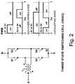
- the concept of the three-state switching cellis for instance described in Ref 2. With the topological circuit described in figure 2 it is possible to improve the performance of energy conversion from an unregulated input to a well regulated output. Those topologies are for high current application and high power, with high efficiency compared to all classical non-isolated DC-DC PWM converters.
- a DC-DC boost converterfor photovoltaic applications, said DC-DC converter comprising:
- the three-state switching cellcomprises switches S1, S2, S3 and S4 where each of the switches is coupled in parallel with a respective voltage balancing circuit.
- the three-state switching cellcomprises a first series connection of switches S1 and S2, each connected in parallel with its individual voltage balancing circuit and a second series connection of switches S3 and S4, each connected in parallel with its individual voltage balancing circuit.
- the voltage balancing circuitsare resistor-capacitor-diode (RCD) networks.
- the switches S1, S2, S3 and S4are silicon MOSFET's or insulated gate bipolar transistors (IGBT).
- the output terminal of the convertermay be coupled to the common (ground) terminal of the converter via a series connection of capacitors.
- the DC-DC boost converter's output terminalis coupled to the common (ground) terminal of the converter via a voltage divider comprising a second capacitor in series with a third capacitor such that a second output terminal is provided at the connection between the second and third capacitors.
- the present inventionrelates to the use of a DC-DC boost converter as disclosed above as a power conditioning converter for photovoltaic devices and systems.
- boost converter according to the present inventionprovides a number of important technical effects, such as: Extremely High efficiency (greater than 99.4%).
- the converter according to the present inventioncan be implemented for any power level, as there is no inherent limitation in the topological circuit.
- the circuitcan also be extended for any number of converters and different kind of connections (series/parallel) using the concept of the three-state switching cell (3SSC).
- SSCthree-state switching cell
- the circuitis applied for PV system but it can be utilized at other applications where DC-DC converter is required.
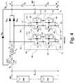
- FIG. 3there is illustrated a schematic diagram of an embodiment of the PWM boost converter according to the invention based on a three-state switching cell (3SSC).
- the converter according to this embodimenthas two input terminals 1, 2 and three output terminals 6, 7 and 8.
- the DC-DC converterreceives input power from any PV array 3, 4 (those connected in series or parallel) providing a voltage in parallel with Ci, 5. It can be seen that the input is connected in series from the input PV source through a flyback transformer Tf, 36, to the 3SSC input CT, 14, which flyback transformer 36 has two windings L B and L S coupled magnetically in a magnetic core with turn-ratio n1:a. From CT, 14, to the output terminal P, 6, the winding L S and the diode D S (this diode can either be a silicon or a silicon carbide diode) 18 are connected. This branch is working as a lossless snubber in order to avoid the recovery current from diodes D B1 and D B2 .
- the three-State switching cellis linked between the output terminals P and N, reference numerals 6 and 8 and the intermediate terminal CT, 14 of a flyback transformer 37.
- the three-state switching cell 21has four terminals 55, 56, 59 and 60, and is consisting of this autotransformer Ta, 37, with turn-ratio n2:1, end terminals 16, 17, respectively, and an intermediate terminal 15.
- the autotransformer 37is acting as a current splitter; two diodes DB1 and DB2, 19, 20, respectively, (which diodes must be silicon diodes) are connected to an output filter and the four switches (S1 - S4), reference numerals 22, 23, 24 and 25, respectively.
- the switches (S1, S2 and S3, S4) of the three-state switching cell 21are respectively connected in series together with their voltage balancing RCD network 26, 27, 28, 29, respectively, to guarantee voltage sharing across each switch.
- the switches S1 through S4can in practice be implemented in different ways, for instance using low voltage silicon MOSFET's or IGBT's as illustrated at 32.
- the switches 22, 23, 24, 25are each coupled in parallel with a separate passive voltage balancing network 26, 27, 28, 29 and the first switch 22 is coupled in series with the second switch 23 and said third switch 24 is coupled in series with said fourth switch 25.
- the passive voltage balancing networks 26, 27, 28, 29each comprise a resistor 47, 48, 49, 50, a capacitor 51, 52, 53, 54 and a diode 43, 44, 45, 46.
- the resistor 47, 48, 49, 50is coupled in parallel with said diode 43, 44, 45, 46, and that this parallel coupling is coupled in series with said capacitor 51, 52, 53, 54.
- the switches 22, 23, 24, 25can for instance be implemented by means of MOSFET's 39, 40, 41, 42, where each separate of the passive voltage balancing networks 26, 27, 28, 29 are coupled between the drain and source terminals of each separate MOSFET with said capacitor 51, 52, 53, 54 coupled to the drain terminal and said parallel connection of a diode 43, 44, 45, 46 and a resistor 47, 48, 49, 50 is coupled to the source terminal of the respective MOSFET.
- the converteris provided with a snubber circuit 18, 36 that is connected between the input terminal 1 and the output terminal 6 of the converter.
- the snubber circuitcomprises a flyback transformer 36, one end terminal 13 of which is connected to the input terminal 1 of the converter, an intermediate terminal 14 that is connected to the intermediate terminal 15 of the first autotransformer 37, where the second end terminal 12 of the flyback transformer 36 is connected to one terminal of a diode 18, the second terminal of which is connected to the output terminal 6 of the converter.
- An output filteris coupled between the P and N output terminals 6, 8 of the converter.
- this filtercomprises a capacitive network comprising capacitors C 1 , C 2 and C 3 , 9, 10 and 11, respectively, but it is understood that other filter configurations may be used instead, and that the application of such alternative filters would fall within the scope of the invention.
- the series connection of C 2 and C 3provides a three-level DC-link P-MP-N voltage to supply any multi-level voltage source inverters.
- the capacitors C 1 , C 2 and C 3could for instance be film-capacitors or electrolytic capacitors.
- FIG 4there is shown an embodiment of the DC-DC converter according to the invention, in which the switches S1 through S4 are implemented using MOSTEF's.
- Figure 4corresponds to figure 3 except from the detailed description of the 3SSC indicated by reference numeral 38 in figure 4 .
- the switches S1, S2, S3 and S4have been implemented by means of MOSFET transistors 39, 40, 41, 42, and the respective voltage balancing RCD network are coupled between each respective MOSFET's source and drain terminals and consists of a capacitor 51, 52, 53, 54 in series with a parallel circuit consisting of a diode 43 in parallel with a resistor as indicated by reference numerals 43, 47; 44, 48; 45, 49 and 46, 50, respectively.
- the input terminals 55 and 56 of the three-state switching cellare coupled to the respective drain terminals of the MOSFTE's 39 and 41, and the respective source terminals of MOSFET's 39 and 41 are connected to the respective drain terminals of the MOSFETS's 40 and 42.
- the source terminals of MOSFET's 40 and 42are both connected to the N-terminal 8 of the converter.
- figure 5(a)shows the states (on/off) of the switches S 1 and S 2 as a function of time; figure 5(b) shows the states (on/off) of the switches S 3 and S 4 as a function of time; figure 5(c) shows the current I LB through the autotransformer 36 from end terminal 13 out of the intermediate terminal 14 hereof as a function of time; figure 5(d) shows the currents I S1 and I S2 through the switches S 1 and S 2 respectively as a function of time; figure 5(e) shows the current I DB1 through the diode 19 in figure 3 as a function of time; figure 5(f) shows the current I DS through the diode 18 in the snubber circuit as a function of time; figure 5(g) shows the voltages V S1 and V S2 over the switches S 1 and S 2 , respectively, as a function of time; figure 5(h) shows the voltage V
- the voltage gaini.e. the ratio between the output voltage Vo and the input voltage Vin of the converter as a function of the duty cycle D of the pulse width modulation (PWM) used in the switching three-state switching cell.
- PWMpulse width modulation
- Ref 1Chung-Yuen Won, a.t. al. "Interleaved Soft-Switching Boost converter for Photovoltaic Power-Generation System", IEEE Transactions on Power Electronics, Vol. 26, No 4, April 2011 .
Landscapes
- Engineering & Computer Science (AREA)
- Power Engineering (AREA)
- Dc-Dc Converters (AREA)
Description
- The present invention relates generally to power conversion, more particularly to PV power conditioning systems with maximum power point tracking (MPPT) and still more particularly to ultra-high efficiency DC-DC PWM converters for solar energy harvesting.
- The developing trends of the AC-DC, DC-DC converters are very high efficiency, high power density, and low cost. With PWM AC/DC, DC-DC Converters it is easier to achieve high efficiency due to their features and simplicity to add soft-switching cells into the main topological circuits. Furthermore, it is possible to increase the switching frequency in order to reduce the size of the reactive components.
- However, there are still certain existing drawbacks regarding the soft-switched PWM converters at high voltage and high power applications, e.g. the high voltage across of switches and the high peak current through the switches resulting in high power losses and large volume of the heat-sinks. Furthermore, the classic PWM converters are less efficient and more difficult to optimize due to the reactive components and suitable semiconductors for high voltage and for high power levels. For instance silicon (Si) technology is being replaced by silicon carbide (SiC) technology, but this technology is still quite expensive today. However, the performance of silicon carbide semiconductors is not as expected in terms of efficiency based in the experiences from practical testing in the laboratory.
- The most widely used converter type for photovoltaic (PV) power conditioning converters found in the industry today is the boost converter with active and passive snubbers, due to its availability the possibility to implement maximum power point tracking (MPPT) and achieve high efficiency. For high current applications and for high power applications in particular, it has been common to use two or more converters and couple them in parallel. This topology has been described in different papers, c.f. for instance Ref. 1.
- When high power is being processed, semiconductors like IGBT, MOSFET, JFET, JBT, diodes, GTO, MCT and others have been the chosen solution for the active switches in the applications found in the industry. However using those devices has been associated with many problems that are limiting the efficiency and/or power density. Among these problems are:
- Current sharing between paralleled devices.
- Reduction of the switching frequency due to the increased commutation losses which increases the weight and the size of the unit.
- Another drawback of the existing solutions is that the voltage-levels are too high and require high voltage semiconductors that are at least capable to handle more than 1.2kV to fulfill the PV system requirements. This reduces the performance and increases the volume, compromising the efficiency of the converter. However the existing silicon carbide technology can solve these kinds of problems, although they are still an expensive solution. Achieving high efficiency in the topological circuits existing in the market today is possible with an increased number of semiconductors (reducing the conduction losses). Further, reducing the switching frequency (to reduce the switching losses) will increase the size of the reactive components, which will increase the power density.
- It is also possible to use silicon carbide semiconductors instead of silicon semiconductors, but this will increase the costs of the converter.
- Further, if the converter is going to be optimized for high power density, the efficiency will be further reduced.
- The choice for optimization in the solutions existing today is either efficiency or high density, but never both, and none of these choices will therefore provide a low cost solution.
- Traditionally, paralleling of converters has been the way to solve the demand for increased DC-power, but due to the issues mentioned above, this is not the optimal solution for high efficiency, and high power density and low cost.Torrico-Bascope G. V. et al "A single phase PFC 3kW converter using a tree-state switching cell", Power Electronics Specialists Conference, 2004. Pesc. 04. 2004 IEEE 35th Annual, Aachen, Germany, 20 - 25 June 2004, Piscataway, NJ, USA, IEEE, US, 20 June 2004, page 4037discloses a related DC-DC boost converter with a three-state switching cell, TSSC, which comprises two functional switches.
EP 0 834 982 A2EP 2 506 413 A2WO 2006/137744 A1 disclose further related DC-DC boost converters. - Torrico-Bascope R. P. et al "A New Isolated DC-DC Boost Converter using Three-State Switching Cell", Applied Power Electronics Conference and Exposition", 2008, APEC 2008, TWENTY-THIRD ANNUAL IEEE, IEEE, PISCATAWAY, NJ, USA, pages 607-613 discloses a snubber circuit comprising a flyback transformer.
- On this background, it is an object of the invention to provide an ultra-high efficiency DC-DC boost converter that overcomes or at least reduces the problems of the prior art.
- On the above background it is an object of the present invention to provide a topological circuit especially suitable for high power, high efficiency, high power density and low cost applications in the art of power electronics for PV power generation systems or others applications, where it can be required.
- In order to overcome the various drawbacks mentioned above, there is according to the invention provided a DC-DC boost converter with which it is possible to achieve very high efficiency, high power density and low cost at least due to following features:
- Simplified implementation of maximum power point tracking (MPPT) for PV system.
- Avoiding the use of silicon carbide semiconductors for high voltage and high frequency.
- Interleaving characteristics of the converter that reduces the current stress through the switches and reduces the number of components of input/output filter.
- Simplified passive snubber avoiding using silicon carbide diodes for the main boost diodes.
- Splitting the power switch in series on each switch in order to reduce the voltage stress and
- consequently reduce the losses and avoiding utilizing silicon carbide semiconductors.
- Simplified and more efficient converter, due to the function of operation of the three-state switching cell used in the converter according to the invention.
- Increased reliability due to a better thermal distribution.
- Simplified and more efficient layout on the converter control strategy of semiconductors, which also reduces the losses.
- An approach that is most suitable for high power is using converters with multilevel features for voltage and current instead.
- In order to reduce the voltage stress when the output voltage is high, a series connection of the semiconductors is recommended. In order to reduce the current stress, connecting the semiconductors in parallel is preferred. In order to increase the efficiency, low voltage semiconductors in series are used, and replacing a single switch with a voltage balancing arrangement network is preferred. The complexity of this is increasing with the number of switches. However, the cost is still lower compared to silicon carbide semiconductors or modules.
- Using standard silicon semiconductors is not only increasing the efficiency, but also simplifying the driving circuitry, reducing the complexity of the drivers that are offered for silicon carbide technology. Furthermore, the discrete solution is also cheaper than the semiconductors module.
- The ripple of the current and voltage in the input and output is higher in the classic solution. Hence, larger input and output filters are required in the classic solution, increasing the volume and cost.
- The reliability of the converter is also increased due to the reduction of the current stress on the semiconductors and the improved thermal distribution in the unit.
- In the converter according to the invention the concept of the three-state switching cell technology has been applied. As described above, the main characteristics of this technology are the possibility to achieve high frequency, high efficiency, high power density and low cost due to the reduction of the losses and avoiding the complexity and the cost using silicon carbide technology.
- Another important feature of the present invention is that the switch on each leg is also split in order to reduce the voltage stress. Two switches are connected in series, each with its own voltage balancing network in parallel with the respective switch and thereby guarantying voltage cascading in semiconductors in order to use low voltage devices to replace high voltage switches.
- The present invention provides significant advantages over alternative solutions that can be obtainable with today's technology. Thus with the circuit according to the present invention it is possible to achieve the desired combination of extremely high efficiency, high power density and low cost.
- The present invention provides a DC-DC boost converter based on the application of the three-state switching cell technology in the converter. As described above, the main characteristics of applying this technology are the possibility to achieve high frequency, high efficiency, high power density, and low cost due to the reduction of the losses and avoiding the complexity and the cost using silicon carbide semiconductors. The concept of the three-state switching cell is for instance described in
Ref 2. With the topological circuit described infigure 2 it is possible to improve the performance of energy conversion from an unregulated input to a well regulated output. Those topologies are for high current application and high power, with high efficiency compared to all classical non-isolated DC-DC PWM converters. - Thus, according to a first aspect of the invention there is provided a DC-DC boost converter for photovoltaic applications, said DC-DC converter comprising:
- (i) an input terminal, an output terminal and a common or ground terminal;
- (ii) a first autotransformer comprising an intermediate terminal and first and second end terminals;
- (iii) a first diode, one terminal of which is coupled to said first end terminal of said first autotransformer;
- (iv) a second diode, one terminal of which is coupled to said second end terminal of said first autotransformer;
- (v) where the second terminals of said diodes are connected to said output terminal;
- (vi) where the output terminal is coupled to said common terminal of the converter through a filter;
- According to an embodiment of the DC-DC boost converter of the invention the three-state switching cell comprises switches S1, S2, S3 and S4 where each of the switches is coupled in parallel with a respective voltage balancing circuit.
- According to an embodiment of the DC-DC boost converter of the invention the three-state switching cell comprises a first series connection of switches S1 and S2, each connected in parallel with its individual voltage balancing circuit and a second series connection of switches S3 and S4, each connected in parallel with its individual voltage balancing circuit.
- According to an embodiment of the DC-DC boost converter of the invention the voltage balancing circuits are resistor-capacitor-diode (RCD) networks.
- According to an embodiment of the DC-DC boost converter of the invention the switches S1, S2, S3 and S4 are silicon MOSFET's or insulated gate bipolar transistors (IGBT).
- In order to provide multi-level output voltages from the converter, the output terminal of the converter may be coupled to the common (ground) terminal of the converter via a series connection of capacitors. According to a specific embodiment of the invention the DC-DC boost converter's output terminal is coupled to the common (ground) terminal of the converter via a voltage divider comprising a second capacitor in series with a third capacitor such that a second output terminal is provided at the connection between the second and third capacitors.
- According to a second aspect, the present invention relates to the use of a DC-DC boost converter as disclosed above as a power conditioning converter for photovoltaic devices and systems.
- A number of important technical effects are provided by the boost converter according to the present invention, such as:
Extremely High efficiency (greater than 99.4%). - High power density due to the reduction of the ripple of current and voltage in the input/output filters due to the characteristics of the topological circuit.
- Low cost for high power application impacting in the size as well as the weight and the volume.
- High reliability due to better thermal distribution.
- Simple autotransformer and PCB assembly.
- The converter according to the present invention can be implemented for any power level, as there is no inherent limitation in the topological circuit.
- The circuit can also be extended for any number of converters and different kind of connections (series/parallel) using the concept of the three-state switching cell (3SSC).
- The circuit is applied for PV system but it can be utilized at other applications where DC-DC converter is required.
- Further objects, features, advantages and properties of the DC-DC boost converter according to the invention will become apparent from the detailed description.
- In the following detailed portion of the description, the invention will be explained in more detail with reference to the exemplary embodiments shown in the drawings, in which:
Figure 1 shows a soft-switching boost converter as described in Reference 1: (a) a single-switch soft-switching boost converter; (b) an interleaved soft switching boost converter (ISSBC);Figure 2 shows the concept of the three-state switching cell (3SSC) as described inReference 2;Figure 3 shows an embodiment of a DC-DC boost converter according to the invention based on the concept of the three-state switching cell with lossless snubber and voltage balance network across switches;Figure 4 shows an embodiment of the invention with the switches implemented by semiconductor configurations;Figure 5 shows key waveforms of operation mode of the converter according to the invention; andFigure 6 shows the voltage gain of the converter according to the invention as a function of duty cycle D.- In the following detailed description of the invention a specific embodiment of a DC-DC boost converter according to the teachings of the present invention will be described.
- Referring to
Figure 3 there is illustrated a schematic diagram of an embodiment of the PWM boost converter according to the invention based on a three-state switching cell (3SSC). The converter according to this embodiment has twoinput terminals output terminals - The DC-DC converter receives input power from any
PV array 3, 4 (those connected in series or parallel) providing a voltage in parallel with Ci, 5. It can be seen that the input is connected in series from the input PV source through a flyback transformer Tf, 36, to the 3SSC input CT, 14, whichflyback transformer 36 has two windings LB and LS coupled magnetically in a magnetic core with turn-ratio n1:a. From CT, 14, to the output terminal P, 6, the winding LS and the diode DS (this diode can either be a silicon or a silicon carbide diode) 18 are connected. This branch is working as a lossless snubber in order to avoid the recovery current from diodes DB1 and DB2. - The three-State switching cell is linked between the output terminals P and N,
reference numerals 6 and 8 and the intermediate terminal CT, 14 of aflyback transformer 37. The three-state switching cell 21 has fourterminals end terminals intermediate terminal 15. Theautotransformer 37 is acting as a current splitter; two diodes DB1 and DB2, 19, 20, respectively, (which diodes must be silicon diodes) are connected to an output filter and the four switches (S1 - S4),reference numerals - The switches (S1, S2 and S3, S4) of the three-
state switching cell 21 are respectively connected in series together with their voltagebalancing RCD network - The
switches voltage balancing network first switch 22 is coupled in series with thesecond switch 23 and saidthird switch 24 is coupled in series with saidfourth switch 25. - The passive
voltage balancing networks resistor capacitor diode resistor diode capacitor - As described in detail below, the
switches voltage balancing networks capacitor diode resistor - According to the invention, the converter is provided with a
snubber circuit input terminal 1 and theoutput terminal 6 of the converter. - The snubber circuit comprises a
flyback transformer 36, one end terminal 13 of which is connected to theinput terminal 1 of the converter, anintermediate terminal 14 that is connected to theintermediate terminal 15 of thefirst autotransformer 37, where thesecond end terminal 12 of theflyback transformer 36 is connected to one terminal of adiode 18, the second terminal of which is connected to theoutput terminal 6 of the converter. - An output filter is coupled between the P and
N output terminals 6, 8 of the converter. In the shown embodiment of the invention, this filter comprises a capacitive network comprising capacitors C1, C2 and C3, 9, 10 and 11, respectively, but it is understood that other filter configurations may be used instead, and that the application of such alternative filters would fall within the scope of the invention. The series connection of C2 and C3 provides a three-level DC-link P-MP-N voltage to supply any multi-level voltage source inverters. The capacitors C1, C2 and C3 could for instance be film-capacitors or electrolytic capacitors. - With reference to
figure 4 there is shown an embodiment of the DC-DC converter according to the invention, in which the switches S1 through S4 are implemented using MOSTEF's.Figure 4 corresponds tofigure 3 except from the detailed description of the 3SSC indicated byreference numeral 38 infigure 4 . - In the embodiment shown in
figure 4 the switches S1, S2, S3 and S4 have been implemented by means ofMOSFET transistors capacitor diode 43 in parallel with a resistor as indicated byreference numerals 43, 47; 44, 48; 45, 49 and 46, 50, respectively. Theinput terminals - With reference to
figure 5 there is shown key waveforms of operation mode of the converter according to the invention. More specifically,figure 5(a) shows the states (on/off) of the switches S1 and S2 as a function of time;figure 5(b) shows the states (on/off) of the switches S3 and S4 as a function of time;figure 5(c) shows the current ILB through theautotransformer 36 from end terminal 13 out of theintermediate terminal 14 hereof as a function of time;figure 5(d) shows the currents IS1 and IS2 through the switches S1 and S2 respectively as a function of time;figure 5(e) shows the current IDB1 through thediode 19 infigure 3 as a function of time;figure 5(f) shows the current IDS through thediode 18 in the snubber circuit as a function of time;figure 5(g) shows the voltages VS1 and VS2 over the switches S1 and S2, respectively, as a function of time;figure 5(h) shows the voltage VDB1 over thediode 19 infigure 3 as a function of time; andfigure 5(i) shows the voltage VDS over thesnubber diode 19 as a function of time. - With reference to
figure 6 there is shown the voltage gain, i.e. the ratio between the output voltage Vo and the input voltage Vin of the converter as a function of the duty cycle D of the pulse width modulation (PWM) used in the switching three-state switching cell. - Although the teaching of this application has been described in detail for purpose of illustration, it is understood that such detail is solely for that purpose, and variations can be made therein by those skilled in the art without departing from the scope of the teaching of this application.
- The term "comprising" as used in the claims does not exclude other elements or steps and the term "a" or "an" as used in the claims does not exclude a plurality.
- Ref 1:Chung-Yuen Won, a.t. al. "Interleaved Soft-Switching Boost converter for Photovoltaic Power-Generation System", IEEE Transactions on Power Electronics, Vol. 26,.
- Ref 2:G. V. T. Bascopé e Ivo Barbi, "Generation of a family of non-isolated DC-DC PWM converters using a three-state switching cell", IEEE 31th Annual Power Electronics Specialists Conference, Volume: 2, pp:858-863, 18-23 June, 2000.
the input terminal of the converter, an intermediate terminal of which flyback transformer is connected to the intermediate terminal of the first autotransformer, and where the second end terminal of the flyback transformer is connected to one terminal of a diode, the second terminal of which is connected to the output terminal of the converter.
Claims (9)
- A DC-DC boost converter for photovoltaic applications, said DC-DC converter comprising:(i) an input terminal (1), an output terminal (6) and a common or ground terminal (8);(ii) a first autotransformer (37) comprising an intermediate terminal (15) and first and second end terminals (16, 17);(iii) a first diode (19), one terminal of which is coupled to said first end terminal (16) of said first autotransformer (37);(iv) a second diode (20), one terminal of which is coupled to said second end terminal (17) of said first autotransformer (37);(v) where the second terminals of said diodes (19, 29) are connected to said output terminal (6);(vi) where the output terminal (6) is coupled to said common terminal (8) of the converter through a filter (9, 10, 11);wherein a three-state switching cell (21) is provided comprising four terminals (55, 56, 59 and 60) and four switches (22, 23, 24, 25), wherein a first terminal (55) is connected to the first switch S1, a second terminal (56) is connected to the second switch S2, a third terminal (59) is connected to the third switch S3 and a fourth terminal (60) is connected to the fourth switch, and wherein said first terminal (55) of the three-state switching cell (21) is connected to said first end terminal (16) of said first autotransformer (37), said third terminal (59) of the three-state switching cell (21) is connected to said second end terminal (17) of said first autotransformer (37) and said second and fourth terminals (56, 60) of the three-state switching cell (21) is connected to said common or ground terminal (8) of the converter,characterized in that a snubber circuit (18, 36) is provided between said input terminal (1) and said output terminal (6) of the converter, wherein said snubber circuit comprises a flyback transformer (36), one end terminal (13) of which is connected to said input terminal (1) of the converter, an intermediate terminal (14) of which flyback transformer (36) is connected to the intermediate terminal (15) of said first autotransformer (37), and where the second end terminal (12) of the flyback transformer (36) is connected to one terminal of a diode (18), the second terminal of which is connected to the output terminal (6) of the converter.
- A DC-DC boost converter according to claim 1, wherein said switches (22, 23, 24, 25) each are coupled in parallel with a separate passive voltage balancing network (26, 27, 28, 29) and that said first switch (22) is coupled in series with said second switch (23) and said third switch (24) is coupled in series with said fourth switch (25).
- A DC-DC boost converter according to claim 2, wherein said passive voltage balancing networks (26, 27, 28, 29) each comprise a resistor (47, 48, 49, 50), a capacitor (51, 52, 53, 54) and a diode (43, 44, 45, 46) .
- A DC-DC boost converter according to claim 3, wherein said resistor (47, 48, 49, 50) is coupled in parallel with said diode (43, 44, 45, 46), and that this parallel coupling is coupled in series with said capacitor (51, 52, 53, 54).
- A DC-DC boost converter according to claim 2, 3 or 4 wherein said switches (22, 23, 24, 25) are implemented by means of MOSFETs (39, 40, 41, 42), where each separate of said passive voltage balancing networks (26, 27, 28, 29) are coupled between the drain and source terminals of each separate MOSFET with said capacitor (51, 52, 53, 54) coupled to the drain terminal and said parallel connection of a diode(43, 44, 45, 46) and a resistor(47, 48, 49, 50) is coupled to the source terminal of the respective MOSFET.
- A DC-DC boost converter according to any of the preceding claims, wherein said first and second diodes (19, 20) are silicon diodes.
- A DC-DC boost converter according to any of the preceding claims, wherein said output terminal (6) is coupled to said common terminal (8) via a voltage divider comprising a second capacitor (10) in series with a third capacitor (11) and that a second output terminal (7) is provided at the connection between the second and third capacitors (10, 11) .
- A DC-DC boost converter according to claim 2, 3 or 4, wherein said switches (22, 23, 24, 25) are implemented by insulated gate bipolar transistors, IGBT's.
- The use of a DC-DC boost converter according to any of the preceding claims 1 to 8 as a power conditioning converter for photovoltaic devices and systems.
Applications Claiming Priority (1)
| Application Number | Priority Date | Filing Date | Title |
|---|---|---|---|
| PCT/EP2013/063413WO2014206463A1 (en) | 2013-06-26 | 2013-06-26 | Dc-dc boost converter for photovoltaic applications based on the concept of the three-state switching cell |
Publications (2)
| Publication Number | Publication Date |
|---|---|
| EP2973974A1 EP2973974A1 (en) | 2016-01-20 |
| EP2973974B1true EP2973974B1 (en) | 2020-05-13 |
Family
ID=48699805
Family Applications (1)
| Application Number | Title | Priority Date | Filing Date |
|---|---|---|---|
| EP13731785.5AActiveEP2973974B1 (en) | 2013-06-26 | 2013-06-26 | Dc-dc boost converter for photovoltaic applications based on the concept of the three-state switching cell |
Country Status (3)
| Country | Link |
|---|---|
| EP (1) | EP2973974B1 (en) |
| CN (1) | CN105612687B (en) |
| WO (1) | WO2014206463A1 (en) |
Cited By (1)
| Publication number | Priority date | Publication date | Assignee | Title |
|---|---|---|---|---|
| US20230132923A1 (en)* | 2019-12-27 | 2023-05-04 | Korea Aerospace Research Institute | Dc-dc conversion device having coupling inductor |
Families Citing this family (7)
| Publication number | Priority date | Publication date | Assignee | Title |
|---|---|---|---|---|
| JP6406130B2 (en)* | 2015-05-28 | 2018-10-17 | 株式会社富士通ゼネラル | Power supply |
| JP6987779B2 (en)* | 2016-04-11 | 2022-01-05 | ワイ−チャージ リミテッド | Optical wireless power supply system |
| KR102005880B1 (en)* | 2017-12-01 | 2019-10-01 | 한국항공우주연구원 | DC to DC Converting System |
| CN108258905B (en)* | 2018-02-12 | 2024-04-12 | 广州金升阳科技有限公司 | Boost circuit and control method thereof |
| CN111934549A (en)* | 2020-07-14 | 2020-11-13 | 中国电子科技集团公司第十八研究所 | Low ripple boost converter |
| KR20230022686A (en)* | 2021-08-09 | 2023-02-16 | 현대자동차주식회사 | Converter using an active clamp and solarcell system having the same |
| DE102023108367A1 (en)* | 2023-03-31 | 2024-10-02 | Infineon Technologies Ag | voltage booster and voltage booster system |
Family Cites Families (5)
| Publication number | Priority date | Publication date | Assignee | Title |
|---|---|---|---|---|
| US5841647A (en)* | 1996-10-07 | 1998-11-24 | Kabushiki Kaisha Toshiba | Power conversion system |
| NO323385B1 (en)* | 2005-06-24 | 2007-04-16 | Eltek Energy As | Control method and device for inverters using a TSSC |
| GB201105145D0 (en)* | 2011-03-28 | 2011-05-11 | Tdk Lambda Uk Ltd | Controller |
| CN102723869A (en)* | 2012-06-13 | 2012-10-10 | 华为技术有限公司 | Power converter |
| CN102931817B (en)* | 2012-10-23 | 2016-03-09 | 华为技术有限公司 | A kind of tri-state switch unit three-phase interleaved converter |
- 2013
- 2013-06-26WOPCT/EP2013/063413patent/WO2014206463A1/enactiveApplication Filing
- 2013-06-26CNCN201380077679.8Apatent/CN105612687B/enactiveActive
- 2013-06-26EPEP13731785.5Apatent/EP2973974B1/enactiveActive
Non-Patent Citations (1)
| Title |
|---|
| RENE P TORRICO-BASCOPE ET AL: "A new isolated DC-DC boost converter using three-state switching cell", APPLIED POWER ELECTRONICS CONFERENCE AND EXPOSITION, 2008. APEC 2008. TWENTY-THIRD ANNUAL IEEE, IEEE, PISCATAWAY, NJ, USA, 24 February 2008 (2008-02-24), pages 607 - 613, XP031253309, ISBN: 978-1-4244-1873-2* |
Cited By (2)
| Publication number | Priority date | Publication date | Assignee | Title |
|---|---|---|---|---|
| US20230132923A1 (en)* | 2019-12-27 | 2023-05-04 | Korea Aerospace Research Institute | Dc-dc conversion device having coupling inductor |
| US12316222B2 (en)* | 2019-12-27 | 2025-05-27 | Korean Aerospace Research Institute | DC-DC conversion device having coupling inductor |
Also Published As
| Publication number | Publication date |
|---|---|
| CN105612687A (en) | 2016-05-25 |
| WO2014206463A1 (en) | 2014-12-31 |
| CN105612687B (en) | 2018-08-14 |
| EP2973974A1 (en) | 2016-01-20 |
Similar Documents
| Publication | Publication Date | Title |
|---|---|---|
| EP2973974B1 (en) | Dc-dc boost converter for photovoltaic applications based on the concept of the three-state switching cell | |
| Revathi et al. | Non isolated high gain DC-DC converter topologies for PV applications–A comprehensive review | |
| Tofoli et al. | Survey on non‐isolated high‐voltage step‐up dc–dc topologies based on the boost converter | |
| EP2571154B1 (en) | PV inverter with input parallel output series connected flyback converters feeding a fullbridge grid converter | |
| Nouri et al. | A non-isolated three-phase high step-up DC–DC converter suitable for renewable energy systems | |
| US20040125618A1 (en) | Multiple energy-source power converter system | |
| KR20060060825A (en) | High Efficiency DC Power Converter with Parallel Power Transmission Method | |
| Siwakoti et al. | Power electronics converters—An overview | |
| AU2009201940A1 (en) | High efficiency, multi-source photovoltaic inverter | |
| EP2514086A2 (en) | Resonant circuit and resonant dc/dc converter | |
| Khalili et al. | Fully soft-switched non-isolated high step-down DC–DC converter with reduced voltage stress and expanding capability | |
| Liao et al. | A GaN-based flying-capacitor multilevel boost converter for high step-up conversion | |
| Hassanpour et al. | Soft-switching bidirectional step-up/down partial power converter with reduced components stress | |
| Surapaneni et al. | A Z-source-derived coupled-inductor-based high voltage gain microinverter | |
| Yu et al. | A novel dual-input ZVS DC/DC converter for low-power energy harvesting applications | |
| Gunawardena et al. | A soft-switched current-fed dual-input isolated DC–DC converter topology | |
| Daryaei et al. | High efficiency and full MPPT range partial power processing PV module-integrated converter | |
| Packnezhad et al. | Fully soft switched interleaved high step-up/down bidirectional converter with no pulsating current at low voltage source | |
| Alcazar et al. | High voltage gain boost converter based on three-state switching cell and voltage multipliers | |
| de Paula et al. | An extensive review of nonisolated DC-DC boost-based converters | |
| Sidorov et al. | High-efficiency quad-mode parallel PV power optimizer for DC microgrids | |
| Yu et al. | Design considerations of a multiple-input isolated single ended primary inductor converter (SEPIC) for distributed generation sources | |
| Gupta et al. | Soft-switching mechanism for a high-gain, interleaved hybrid boost converter | |
| Salvador et al. | Nonisolated high step‐up DC‐DC interleaved SEPIC converter based on voltage multiplier cells | |
| Wu et al. | ZVS three‐phase current‐fed push–pull converter employing a simple active‐clamp circuit for voltage step‐up applications |
Legal Events
| Date | Code | Title | Description |
|---|---|---|---|
| PUAI | Public reference made under article 153(3) epc to a published international application that has entered the european phase | Free format text:ORIGINAL CODE: 0009012 | |
| 17P | Request for examination filed | Effective date:20151015 | |
| AK | Designated contracting states | Kind code of ref document:A1 Designated state(s):AL AT BE BG CH CY CZ DE DK EE ES FI FR GB GR HR HU IE IS IT LI LT LU LV MC MK MT NL NO PL PT RO RS SE SI SK SM TR | |
| AX | Request for extension of the european patent | Extension state:BA ME | |
| RIN1 | Information on inventor provided before grant (corrected) | Inventor name:TORRICO-BASCOPE, GROVER VICTOR Inventor name:MA, JUN | |
| DAX | Request for extension of the european patent (deleted) | ||
| STAA | Information on the status of an ep patent application or granted ep patent | Free format text:STATUS: EXAMINATION IS IN PROGRESS | |
| 17Q | First examination report despatched | Effective date:20190529 | |
| GRAP | Despatch of communication of intention to grant a patent | Free format text:ORIGINAL CODE: EPIDOSNIGR1 | |
| STAA | Information on the status of an ep patent application or granted ep patent | Free format text:STATUS: GRANT OF PATENT IS INTENDED | |
| RIC1 | Information provided on ipc code assigned before grant | Ipc:H02M 3/158 20060101AFI20200120BHEP Ipc:H02M 1/00 20060101ALI20200120BHEP | |
| INTG | Intention to grant announced | Effective date:20200207 | |
| GRAS | Grant fee paid | Free format text:ORIGINAL CODE: EPIDOSNIGR3 | |
| GRAA | (expected) grant | Free format text:ORIGINAL CODE: 0009210 | |
| STAA | Information on the status of an ep patent application or granted ep patent | Free format text:STATUS: THE PATENT HAS BEEN GRANTED | |
| AK | Designated contracting states | Kind code of ref document:B1 Designated state(s):AL AT BE BG CH CY CZ DE DK EE ES FI FR GB GR HR HU IE IS IT LI LT LU LV MC MK MT NL NO PL PT RO RS SE SI SK SM TR | |
| REG | Reference to a national code | Ref country code:GB Ref legal event code:FG4D | |
| REG | Reference to a national code | Ref country code:CH Ref legal event code:EP | |
| REG | Reference to a national code | Ref country code:DE Ref legal event code:R096 Ref document number:602013069055 Country of ref document:DE | |
| REG | Reference to a national code | Ref country code:AT Ref legal event code:REF Ref document number:1271556 Country of ref document:AT Kind code of ref document:T Effective date:20200615 | |
| REG | Reference to a national code | Ref country code:LT Ref legal event code:MG4D | |
| REG | Reference to a national code | Ref country code:NL Ref legal event code:MP Effective date:20200513 | |
| PG25 | Lapsed in a contracting state [announced via postgrant information from national office to epo] | Ref country code:SE Free format text:LAPSE BECAUSE OF FAILURE TO SUBMIT A TRANSLATION OF THE DESCRIPTION OR TO PAY THE FEE WITHIN THE PRESCRIBED TIME-LIMIT Effective date:20200513 Ref country code:NO Free format text:LAPSE BECAUSE OF FAILURE TO SUBMIT A TRANSLATION OF THE DESCRIPTION OR TO PAY THE FEE WITHIN THE PRESCRIBED TIME-LIMIT Effective date:20200813 Ref country code:GR Free format text:LAPSE BECAUSE OF FAILURE TO SUBMIT A TRANSLATION OF THE DESCRIPTION OR TO PAY THE FEE WITHIN THE PRESCRIBED TIME-LIMIT Effective date:20200814 Ref country code:LT Free format text:LAPSE BECAUSE OF FAILURE TO SUBMIT A TRANSLATION OF THE DESCRIPTION OR TO PAY THE FEE WITHIN THE PRESCRIBED TIME-LIMIT Effective date:20200513 Ref country code:PT Free format text:LAPSE BECAUSE OF FAILURE TO SUBMIT A TRANSLATION OF THE DESCRIPTION OR TO PAY THE FEE WITHIN THE PRESCRIBED TIME-LIMIT Effective date:20200914 Ref country code:FI Free format text:LAPSE BECAUSE OF FAILURE TO SUBMIT A TRANSLATION OF THE DESCRIPTION OR TO PAY THE FEE WITHIN THE PRESCRIBED TIME-LIMIT Effective date:20200513 Ref country code:IS Free format text:LAPSE BECAUSE OF FAILURE TO SUBMIT A TRANSLATION OF THE DESCRIPTION OR TO PAY THE FEE WITHIN THE PRESCRIBED TIME-LIMIT Effective date:20200913 | |
| PG25 | Lapsed in a contracting state [announced via postgrant information from national office to epo] | Ref country code:LV Free format text:LAPSE BECAUSE OF FAILURE TO SUBMIT A TRANSLATION OF THE DESCRIPTION OR TO PAY THE FEE WITHIN THE PRESCRIBED TIME-LIMIT Effective date:20200513 Ref country code:HR Free format text:LAPSE BECAUSE OF FAILURE TO SUBMIT A TRANSLATION OF THE DESCRIPTION OR TO PAY THE FEE WITHIN THE PRESCRIBED TIME-LIMIT Effective date:20200513 Ref country code:RS Free format text:LAPSE BECAUSE OF FAILURE TO SUBMIT A TRANSLATION OF THE DESCRIPTION OR TO PAY THE FEE WITHIN THE PRESCRIBED TIME-LIMIT Effective date:20200513 Ref country code:BG Free format text:LAPSE BECAUSE OF FAILURE TO SUBMIT A TRANSLATION OF THE DESCRIPTION OR TO PAY THE FEE WITHIN THE PRESCRIBED TIME-LIMIT Effective date:20200813 | |
| REG | Reference to a national code | Ref country code:AT Ref legal event code:MK05 Ref document number:1271556 Country of ref document:AT Kind code of ref document:T Effective date:20200513 | |
| PG25 | Lapsed in a contracting state [announced via postgrant information from national office to epo] | Ref country code:NL Free format text:LAPSE BECAUSE OF FAILURE TO SUBMIT A TRANSLATION OF THE DESCRIPTION OR TO PAY THE FEE WITHIN THE PRESCRIBED TIME-LIMIT Effective date:20200513 Ref country code:AL Free format text:LAPSE BECAUSE OF FAILURE TO SUBMIT A TRANSLATION OF THE DESCRIPTION OR TO PAY THE FEE WITHIN THE PRESCRIBED TIME-LIMIT Effective date:20200513 | |
| PG25 | Lapsed in a contracting state [announced via postgrant information from national office to epo] | Ref country code:ES Free format text:LAPSE BECAUSE OF FAILURE TO SUBMIT A TRANSLATION OF THE DESCRIPTION OR TO PAY THE FEE WITHIN THE PRESCRIBED TIME-LIMIT Effective date:20200513 Ref country code:RO Free format text:LAPSE BECAUSE OF FAILURE TO SUBMIT A TRANSLATION OF THE DESCRIPTION OR TO PAY THE FEE WITHIN THE PRESCRIBED TIME-LIMIT Effective date:20200513 Ref country code:CZ Free format text:LAPSE BECAUSE OF FAILURE TO SUBMIT A TRANSLATION OF THE DESCRIPTION OR TO PAY THE FEE WITHIN THE PRESCRIBED TIME-LIMIT Effective date:20200513 Ref country code:IT Free format text:LAPSE BECAUSE OF FAILURE TO SUBMIT A TRANSLATION OF THE DESCRIPTION OR TO PAY THE FEE WITHIN THE PRESCRIBED TIME-LIMIT Effective date:20200513 Ref country code:SM Free format text:LAPSE BECAUSE OF FAILURE TO SUBMIT A TRANSLATION OF THE DESCRIPTION OR TO PAY THE FEE WITHIN THE PRESCRIBED TIME-LIMIT Effective date:20200513 Ref country code:AT Free format text:LAPSE BECAUSE OF FAILURE TO SUBMIT A TRANSLATION OF THE DESCRIPTION OR TO PAY THE FEE WITHIN THE PRESCRIBED TIME-LIMIT Effective date:20200513 Ref country code:DK Free format text:LAPSE BECAUSE OF FAILURE TO SUBMIT A TRANSLATION OF THE DESCRIPTION OR TO PAY THE FEE WITHIN THE PRESCRIBED TIME-LIMIT Effective date:20200513 Ref country code:EE Free format text:LAPSE BECAUSE OF FAILURE TO SUBMIT A TRANSLATION OF THE DESCRIPTION OR TO PAY THE FEE WITHIN THE PRESCRIBED TIME-LIMIT Effective date:20200513 | |
| REG | Reference to a national code | Ref country code:CH Ref legal event code:PL | |
| REG | Reference to a national code | Ref country code:DE Ref legal event code:R097 Ref document number:602013069055 Country of ref document:DE | |
| PG25 | Lapsed in a contracting state [announced via postgrant information from national office to epo] | Ref country code:SK Free format text:LAPSE BECAUSE OF FAILURE TO SUBMIT A TRANSLATION OF THE DESCRIPTION OR TO PAY THE FEE WITHIN THE PRESCRIBED TIME-LIMIT Effective date:20200513 Ref country code:MC Free format text:LAPSE BECAUSE OF FAILURE TO SUBMIT A TRANSLATION OF THE DESCRIPTION OR TO PAY THE FEE WITHIN THE PRESCRIBED TIME-LIMIT Effective date:20200513 Ref country code:PL Free format text:LAPSE BECAUSE OF FAILURE TO SUBMIT A TRANSLATION OF THE DESCRIPTION OR TO PAY THE FEE WITHIN THE PRESCRIBED TIME-LIMIT Effective date:20200513 | |
| PLBE | No opposition filed within time limit | Free format text:ORIGINAL CODE: 0009261 | |
| STAA | Information on the status of an ep patent application or granted ep patent | Free format text:STATUS: NO OPPOSITION FILED WITHIN TIME LIMIT | |
| PG25 | Lapsed in a contracting state [announced via postgrant information from national office to epo] | Ref country code:LU Free format text:LAPSE BECAUSE OF NON-PAYMENT OF DUE FEES Effective date:20200626 | |
| REG | Reference to a national code | Ref country code:BE Ref legal event code:MM Effective date:20200630 | |
| 26N | No opposition filed | Effective date:20210216 | |
| PG25 | Lapsed in a contracting state [announced via postgrant information from national office to epo] | Ref country code:LI Free format text:LAPSE BECAUSE OF NON-PAYMENT OF DUE FEES Effective date:20200630 Ref country code:IE Free format text:LAPSE BECAUSE OF NON-PAYMENT OF DUE FEES Effective date:20200626 Ref country code:CH Free format text:LAPSE BECAUSE OF NON-PAYMENT OF DUE FEES Effective date:20200630 | |
| PG25 | Lapsed in a contracting state [announced via postgrant information from national office to epo] | Ref country code:SI Free format text:LAPSE BECAUSE OF FAILURE TO SUBMIT A TRANSLATION OF THE DESCRIPTION OR TO PAY THE FEE WITHIN THE PRESCRIBED TIME-LIMIT Effective date:20200513 Ref country code:BE Free format text:LAPSE BECAUSE OF NON-PAYMENT OF DUE FEES Effective date:20200630 | |
| REG | Reference to a national code | Ref country code:GB Ref legal event code:732E Free format text:REGISTERED BETWEEN 20211111 AND 20211117 | |
| REG | Reference to a national code | Ref country code:DE Ref legal event code:R081 Ref document number:602013069055 Country of ref document:DE Owner name:HUAWEI DIGITAL POWER TECHNOLOGIES CO., LTD., S, CN Free format text:FORMER OWNER: HUAWEI TECHNOLOGIES CO., LTD., SHENZHEN, GUANGDONG, CN | |
| PG25 | Lapsed in a contracting state [announced via postgrant information from national office to epo] | Ref country code:TR Free format text:LAPSE BECAUSE OF FAILURE TO SUBMIT A TRANSLATION OF THE DESCRIPTION OR TO PAY THE FEE WITHIN THE PRESCRIBED TIME-LIMIT Effective date:20200513 Ref country code:MT Free format text:LAPSE BECAUSE OF FAILURE TO SUBMIT A TRANSLATION OF THE DESCRIPTION OR TO PAY THE FEE WITHIN THE PRESCRIBED TIME-LIMIT Effective date:20200513 Ref country code:CY Free format text:LAPSE BECAUSE OF FAILURE TO SUBMIT A TRANSLATION OF THE DESCRIPTION OR TO PAY THE FEE WITHIN THE PRESCRIBED TIME-LIMIT Effective date:20200513 | |
| PG25 | Lapsed in a contracting state [announced via postgrant information from national office to epo] | Ref country code:MK Free format text:LAPSE BECAUSE OF FAILURE TO SUBMIT A TRANSLATION OF THE DESCRIPTION OR TO PAY THE FEE WITHIN THE PRESCRIBED TIME-LIMIT Effective date:20200513 | |
| P01 | Opt-out of the competence of the unified patent court (upc) registered | Effective date:20230524 | |
| PGFP | Annual fee paid to national office [announced via postgrant information from national office to epo] | Ref country code:DE Payment date:20250429 Year of fee payment:13 | |
| PGFP | Annual fee paid to national office [announced via postgrant information from national office to epo] | Ref country code:GB Payment date:20250508 Year of fee payment:13 | |
| PGFP | Annual fee paid to national office [announced via postgrant information from national office to epo] | Ref country code:FR Payment date:20250508 Year of fee payment:13 |