EP2972280B1 - Chemical sensor with consistent sensor surface areas - Google Patents
Chemical sensor with consistent sensor surface areasDownload PDFInfo
- Publication number
- EP2972280B1 EP2972280B1EP14712488.7AEP14712488AEP2972280B1EP 2972280 B1EP2972280 B1EP 2972280B1EP 14712488 AEP14712488 AEP 14712488AEP 2972280 B1EP2972280 B1EP 2972280B1
- Authority
- EP
- European Patent Office
- Prior art keywords
- dielectric
- conductive element
- opening
- chemical sensor
- floating gate
- Prior art date
- Legal status (The legal status is an assumption and is not a legal conclusion. Google has not performed a legal analysis and makes no representation as to the accuracy of the status listed.)
- Active
Links
Images


Classifications
- G—PHYSICS
- G01—MEASURING; TESTING
- G01N—INVESTIGATING OR ANALYSING MATERIALS BY DETERMINING THEIR CHEMICAL OR PHYSICAL PROPERTIES
- G01N27/00—Investigating or analysing materials by the use of electric, electrochemical, or magnetic means
- G01N27/26—Investigating or analysing materials by the use of electric, electrochemical, or magnetic means by investigating electrochemical variables; by using electrolysis or electrophoresis
- G01N27/403—Cells and electrode assemblies
- G01N27/414—Ion-sensitive or chemical field-effect transistors, i.e. ISFETS or CHEMFETS
- G01N27/4148—Integrated circuits therefor, e.g. fabricated by CMOS processing
- B—PERFORMING OPERATIONS; TRANSPORTING
- B01—PHYSICAL OR CHEMICAL PROCESSES OR APPARATUS IN GENERAL
- B01L—CHEMICAL OR PHYSICAL LABORATORY APPARATUS FOR GENERAL USE
- B01L3/00—Containers or dishes for laboratory use, e.g. laboratory glassware; Droppers
- B01L3/50—Containers for the purpose of retaining a material to be analysed, e.g. test tubes
- B01L3/502—Containers for the purpose of retaining a material to be analysed, e.g. test tubes with fluid transport, e.g. in multi-compartment structures
- B01L3/5027—Containers for the purpose of retaining a material to be analysed, e.g. test tubes with fluid transport, e.g. in multi-compartment structures by integrated microfluidic structures, i.e. dimensions of channels and chambers are such that surface tension forces are important, e.g. lab-on-a-chip
- B01L3/502761—Containers for the purpose of retaining a material to be analysed, e.g. test tubes with fluid transport, e.g. in multi-compartment structures by integrated microfluidic structures, i.e. dimensions of channels and chambers are such that surface tension forces are important, e.g. lab-on-a-chip specially adapted for handling suspended solids or molecules independently from the bulk fluid flow, e.g. for trapping or sorting beads, for physically stretching molecules
- H—ELECTRICITY
- H10—SEMICONDUCTOR DEVICES; ELECTRIC SOLID-STATE DEVICES NOT OTHERWISE PROVIDED FOR
- H10D—INORGANIC ELECTRIC SEMICONDUCTOR DEVICES
- H10D64/00—Electrodes of devices having potential barriers
- H10D64/01—Manufacture or treatment
- H10D64/031—Manufacture or treatment of data-storage electrodes
- H10D64/035—Manufacture or treatment of data-storage electrodes comprising conductor-insulator-conductor-insulator-semiconductor structures
- B—PERFORMING OPERATIONS; TRANSPORTING
- B01—PHYSICAL OR CHEMICAL PROCESSES OR APPARATUS IN GENERAL
- B01L—CHEMICAL OR PHYSICAL LABORATORY APPARATUS FOR GENERAL USE
- B01L2200/00—Solutions for specific problems relating to chemical or physical laboratory apparatus
- B01L2200/06—Fluid handling related problems
- B01L2200/0647—Handling flowable solids, e.g. microscopic beads, cells, particles
- B01L2200/0668—Trapping microscopic beads
- B—PERFORMING OPERATIONS; TRANSPORTING
- B01—PHYSICAL OR CHEMICAL PROCESSES OR APPARATUS IN GENERAL
- B01L—CHEMICAL OR PHYSICAL LABORATORY APPARATUS FOR GENERAL USE
- B01L2300/00—Additional constructional details
- B01L2300/06—Auxiliary integrated devices, integrated components
- B01L2300/0627—Sensor or part of a sensor is integrated
- B01L2300/0636—Integrated biosensor, microarrays
- B—PERFORMING OPERATIONS; TRANSPORTING
- B01—PHYSICAL OR CHEMICAL PROCESSES OR APPARATUS IN GENERAL
- B01L—CHEMICAL OR PHYSICAL LABORATORY APPARATUS FOR GENERAL USE
- B01L2300/00—Additional constructional details
- B01L2300/08—Geometry, shape and general structure
- B01L2300/0861—Configuration of multiple channels and/or chambers in a single devices
- B01L2300/0877—Flow chambers
- G—PHYSICS
- G01—MEASURING; TESTING
- G01N—INVESTIGATING OR ANALYSING MATERIALS BY DETERMINING THEIR CHEMICAL OR PHYSICAL PROPERTIES
- G01N27/00—Investigating or analysing materials by the use of electric, electrochemical, or magnetic means
- G01N27/26—Investigating or analysing materials by the use of electric, electrochemical, or magnetic means by investigating electrochemical variables; by using electrolysis or electrophoresis
- G01N27/403—Cells and electrode assemblies
- G01N27/414—Ion-sensitive or chemical field-effect transistors, i.e. ISFETS or CHEMFETS
- G01N27/4145—Ion-sensitive or chemical field-effect transistors, i.e. ISFETS or CHEMFETS specially adapted for biomolecules, e.g. gate electrode with immobilised receptors
Definitions
- the present disclosurerelates to sensors for chemical analysis, and to methods for manufacturing such sensors.
- a variety of types of chemical sensorshave been used in the detection of chemical processes.
- One typeis a chemically-sensitive field effect transistor (chemFET).
- a chemFETincludes a source and a drain separated by a channel region, and a chemically sensitive area coupled to the channel region.
- the operation of the chemFETis based on the modulation of channel conductance, caused by changes in charge at the sensitive area due to a chemical reaction occurring nearby.
- the modulation of the channel conductancechanges the threshold voltage of the chemFET, which can be measured to detect and/or determine characteristics of the chemical reaction.
- the threshold voltagemay for example be measured by applying appropriate bias voltages to the source and drain, and measuring a resulting current flowing through the chemFET.
- the threshold voltagemay be measured by driving a known current through the chemFET, and measuring a resulting voltage at the source or drain.
- ISFETion-sensitive field effect transistor
- An ion-sensitive field effect transistoris a type of chemFET that includes an ion-sensitive layer at the sensitive area.
- the presence of ions in an analyte solutionalters the surface potential at the interface between the ion-sensitive layer and the analyte solution, due to the protonation or deprotonation of surface charge groups caused by the ions present in the analyte solution.
- the change in surface potential at the sensitive area of the ISFETaffects the threshold voltage of the device, which can be measured to indicate the presence and/or concentration of ions within the solution.
- Arrays of ISFETsmay be used for monitoring chemical reactions, such as DNA sequencing reactions, based on the detection of ions present, generated, or used during the reactions.
- chemFETsor other types of chemical sensors may be employed to detect and measure static and/or dynamic amounts or concentrations of a variety of analytes (e.g. hydrogen ions, other ions, compounds, etc.) in a variety of processes.
- the processesmay for example be biological or chemical reactions, cell or tissue cultures or monitoring neural activity, nucleic acid sequencing, etc.
- a chemical sensorin one embodiment, includes a chemically-sensitive field effect transistor including a floating gate conductor having an upper surface; a material defining an opening extending to the upper surface of the floating gate conductor, the material comprising a first dielectric underlying a second dielectric; and a conductive element contacting the upper surface of the floating gate conductor and extending a distance along a sidewall of the opening, wherein the conductive element extends along the sidewall between 5% of the sidewall and 85% of the sidewall .
- the opening of the chemical sensormay include a lower portion within the first dielectric, and an upper portion within the second dielectric.
- a width of the lower portion of the openingis substantially the same as a width of the upper portion.
- the conductive elementis conformal with a shape of the opening.
- the conductive elementextends to an upper surface of the second dielectric.
- the conductive elementincludes an inner surface defining a lower portion of a reaction region for the chemical sensor, and the second dielectric includes an inner surface defining an upper portion of the opening.
- the conductive elementcomprises an electrically conductive material, and an inner surface of the conductive element includes an oxide of the electrically conductive material.
- a sensing surface of the chemical sensorincludes an inner surface of the conductive element.
- the chemically-sensitive field effect transistorgenerates a sensor signal in response to a chemical reaction occurring proximate to the conductive element.
- the floating gate conductorcomprises a plurality of conductors electrically coupled to one another and separated by dielectric layers, and the floating gate conductor is an uppermost conductor in the plurality of conductors.
- a method for manufacturing a chemical sensorincludes forming a chemically-sensitive field effect transistor including a floating gate conductor having an upper surface; forming a material defining an opening extending to the upper surface of the floating gate conductor, the material comprising a first dielectric underlying a second dielectric; and forming a conductive element contacting the upper surface of the floating gate conductor and extending a distance along a sidewall of the opening, wherein the conductive element extends along the sidewall between 5% of the sidewall and 85% of the sidewall .
- forming the material and forming the conductive elementmay include forming the first dielectric on the floating gate conductor, the first dielectric defining a cavity extending to the upper surface of the floating gate conductor; forming the second dielectric thereon; etching the second dielectric to expose the conductive element, thereby defining an opening; and forming the conductive element within the opening.
- forming the conductive element within the openingmay include depositing a conductive material within the opening and on an upper surface of the first dielectric; and removing at least a portion of the conductive material from the upper surface of the second dielectric.
- removing at least the portion of the conductive materialmay comprises depositing a layer of photoresist within the opening; and removing at least a portion of the conductive material together with the photoresist from the upper surface of the second dielectric.
- the conductive materialcomprises titanium.
- the openingis a nanowell.
- the forming a conductive elementincludes depositing a conductive material conformally within the opening.
- the conductive elementincludes an inner surface defining a lower portion of a reaction region for the chemical sensor, and the second dielectric includes an inner surface defining an upper portion of the opening.
- a chemical detection deviceincludes low noise chemical sensors, such as chemically-sensitive field effect transistors (chemFETs), for detecting chemical reactions within overlying, operationally associated reaction regions. Reducing the plan or top view area (or footprint) of individual chemical sensors and the overlying reaction regions allows for higher density devices. However, as the dimensions of the chemical sensors are reduced, Applicants have found that a corresponding reduction in the sensing surface area of the sensors can significantly impact performance. For example, for chemical sensors having sensing surfaces defined at the bottom of the reaction regions, reducing the plan view dimensions (e.g. the width or diameter) of the reaction regions results in a similar reduction in the sensing surface areas.
- chemFETschemically-sensitive field effect transistors
- Chemical sensors described hereinhave sensing surface areas which are not limited to a two-dimensional area at the bottom of the reaction regions.
- the sensing surface of the chemical sensorincludes a generally horizontal portion along the bottom surface of the reaction region, as well as a generally vertical portion extending along a sidewall of an opening containing the reaction region. The distance that the generally vertical portion extends along the sidewall is defined by the thickness of a dielectric material that forms a lower portion of the opening.
- the dielectric materialcan be deposited using a process (e.g. thin film deposition) which results in very small thickness variation across the array. In doing so, the sensor surface areas of the chemical sensors can be very well controlled, resulting in uniform chemical sensor performance across the array and thus simplifying the downstream signal processing.
- the chemical sensorBy extending the sensing surface in the generally vertical direction, the chemical sensor can have a small footprint, while also having a sufficiently large sensing surface area to avoid the noise issues associated with small sensing surfaces.
- the footprint of a chemical sensoris determined in part by the width (e.g. diameter) of the overlying reaction region and can be made small, allowing for a high density array.
- the sensing surfaceextends a controlled distance up the sidewall, the sensing surface area can be relatively large. As a result, low noise chemical sensors can be provided in a high density array, such that the characteristics of reactions can be accurately dctcctcd.
- FIG. 1illustrates a block diagram of components of a system for nucleic acid sequencing according to an exemplary embodiment.
- the componentsinclude a flow cell 101 on an integrated circuit device 100, a reference electrode 108, a plurality of reagents 114 for sequencing, a valve block 116, a wash solution 110, a valve 112, a fluidics controller 118, lines 120/122/126, passages 104/109/111, a waste container 106, an array controller 124, and a user interface 128.
- the integrated circuit device 100includes a microwell array 107 overlying a sensor array that includes chemical sensors as described herein.
- the flow cell 101includes an inlet 102, an outlet 103, and a flow chamber 105 defining a flow path for the reagents 114 over the microwell array 107.
- the reference electrode 108may be of any suitable type or shape, including a concentric cylinder with a fluid passage or a wire inserted into a lumen of passage 111.
- the reagents 114may be driven through the fluid pathways, valves, and flow cell 101 by pumps, gas pressure, vacuum, or other suitable methods, and may be discarded into the waste container 106 after exiting the outlet 103 of the flow cell 101.
- the fluidics controller 118may control driving forces for the reagents 114 and the operation of valve 112 and valve block 116 with suitable software.
- the microwell array 107includes reaction regions, also referred to herein as microwells, which are operationally associated with corresponding chemical sensors in the sensor array. For example, each reaction region may be coupled to a chemical sensor suitable for detecting an analyte or reaction property of interest within that reaction region.
- the microwell array 107may be integrated in the integrated circuit device 100, so that the microwell array 107 and the sensor array are part of a single device or chip.
- the flow cell 101may have a variety of configurations for controlling the path and flow rate of reagents 114 over the microwell array 107.
- the array controller 124provides bias voltages and timing and control signals to the integrated circuit device 100 for reading the chemical sensors of the sensor array.
- the array controller 124also provides a reference bias voltage to the reference electrode 108 to bias the reagents 114 flowing over the microwell array 107.
- the array controller 124collects and processes output signals from the chemical sensors of the sensor array through output ports on the integrated circuit device 100 via bus 127.
- the array controller 124may be a computer or other computing means.
- the array controller 124may include memory for storage of data and software applications, a processor for accessing data and executing applications, and components that facilitate communication with the various components of the system in FIG. 1 .
- the array controller 124is external to the integrated circuit device 100. In some alternative embodiments, some or all of the functions performed by the array controller 124 are carried out by a controller or other data processor on the integrated circuit device 100.
- the values of the output signals from the chemical sensorsindicate physical and/or chemical parameters of one or more reactions taking place in the corresponding reaction regions in the microwell array 107.
- the values of the output signalsmay be processed using the techniques disclosed in Rearick et al., U.S. Pat. Appl. No. 13/339,846, filed December 29, 2011 , based on U.S. Prov. Pat. Appl. Nos. 61/428,743, filed December 30, 2010 , and 61/429,328, filed January 3, 2011 , and in Hubbell, U.S. Pat. Appl. No. 13/339,753, filed December 29, 2011 , based on U.S. Prov. Pat. Appl.
- the user interface 128may display information about the flow cell 101 and the output signals received from chemical sensors in the sensor array on the integrated circuit device 100.
- the user interface 128may also display instrument settings and controls, and allow a user to enter or set instrument settings and controls.
- the fluidics controller 118may control delivery of the individual reagents 114 to the flow cell 101 and integrated circuit device 100 in a predetermined sequence, for predetermined durations, at predetermined flow rates.
- the array controller 124can then collect and analyze the output signals of the chemical sensors indicating chemical reactions occurring in response to the delivery of the reagents 114.
- the systemmay also monitor and control the temperature of the integrated circuit device 100, so that reactions take place and measurements are made at a known predetermined temperature.
- the systemmay be configured to let a single fluid or reagent contact the reference electrode 108 throughout an entire multi-step reaction during operation.
- the valve 112may be shut to prevent any wash solution 110 from flowing into passage 109 as the reagents 114 are flowing. Although the flow of wash solution may be stopped, there may still be uninterrupted fluid and electrical communication between the reference electrode 108, passage 109, and the microwell array 107.
- the distance between the reference electrode 108 and the junction between passages 109 and 111may be selected so that little or no amount of the reagents flowing in passage 109 (and possibly diffusing into passage 111) reach the reference electrode 108.
- the wash solution 110may be selected as being in continuous contact with the reference electrode 108, which may be especially useful for multi-step reactions using frequent wash steps.
- FIG. 2illustrates cross-sectional and expanded views of a portion of the integrated circuit device 100 and flow cell 101.
- the integrated circuit device 100includes the microwell array 107 of reaction regions operationally associated with sensor array 205.
- the flow chamber 105 of the flow cell 101confines a reagent flow 208 of delivered reagents across open ends of the reaction regions in the microwell array 107.
- the volume, shape, aspect ratio (such as base width-to-well depth ratio), and other dimensional characteristics of the reaction regionsmay be selected based on the nature of the reaction taking place, as well as the reagents, byproducts, or labeling techniques (if any) that are employed.
- the chemical sensors of the sensor array 205are responsive to (and generate output signals related to) chemical reactions within associated reaction regions in the microwell array 107 to detect an analyte or reaction property of interest.
- the chemical sensors of the sensor array 205may for example be chemically sensitive field-effect transistors (chemFETs), such as ion-sensitive field effect transistors (ISFETs). Examples of chemical sensors and array configurations that may be used in embodiments are described in Schultz et al., U.S. Pat. Appl. No. 12/785,667 (now U.S. Patent No. 8,546,128), filed May 24, 2010 , titled "Fluidics System for Sequential Delivery of Reagents"; Rotherberg et al., U.S. Pat.
- FIG. 3illustrates a cross-sectional view of two representative chemical sensors and their corresponding reaction regions according to a first embodiment.
- two chemical sensors 350, 351are shown, representing a small portion of a sensor array that can include millions of chemical sensors.
- Chemical sensor 350is coupled to corresponding reaction region 301, and chemical sensor 351 is coupled to corresponding reaction region 302.
- Chemical sensor 350is representative of the chemical sensors in the sensor array.
- the chemical sensor 350is a chemically-sensitive field effect transistor (chemFET), more specifically an ion-sensitive field effect transistor (ISFET) in this example.
- the chemical sensor 350includes a floating gate structure 318 having a sensor plate 320 coupled to the reaction region 301 by an electrically conductive element 370.
- the sensor plate 320is the uppermost floating gate conductor in the floating gate structure 318.
- the floating gate structure 318includes multiple patterned layers of conductive material within layers of dielectric material 319.
- the chemical sensor 350also includes a source region 321 and a drain region 322 within a semiconductor substrate 354.
- the source region 321 and the drain region 322comprise doped semiconductor material have a conductivity type different from the conductivity type of the substrate 354.
- the source region 321 and the drain region 322may comprise doped P-type semiconductor material, and the substrate may comprise doped N-type semiconductor material.
- Channel region 323separates the source region 321 and the drain region 322.
- the floating gate structure 318overlies the channel region 323, and is separated from the substrate 354 by a gate dielectric 352.
- the gate dielectric 352may be for example silicon dioxide. Alternatively, other dielectrics may be used for the gate dielectric 352.
- the reaction region 301is within an opening having a sidewall 303 extending through dielectric materials 310, 308 to the upper surface of the sensor plate 320.
- Each of the dielectric materials 310, 308may comprise one or more layers of material, such as silicon dioxide or silicon nitride.
- the openingincludes a lower portion 314 within dielectric material 308 and proximate to the sensor plate 320.
- the openingalso includes an upper portion 315 within the dielectric material 310 and extending from the lower portion 314 to the upper surface of the dielectric material 310.
- the width of the upper portion 315 of the openingis substantially the same as the width of the lower portion 314 of the opening.
- the width of the upper portion 315 of the openingmay be greater than the width of the lower portion 314 of the opening, or vice versa.
- the openingmay for example have a circular cross-section.
- the openingmay be non-circular.
- the cross-sectionmay be square, rectangular, hexagonal, or irregularly shaped.
- the dimensions of the openings, and their pitch,can vary from embodiment to embodiment.
- the openingscan have a characteristic diameter, defined as the square root of 4 times the plan view cross-sectional area (A) divided by Pi (e.g., sqrt(4 ⁇ A/ ⁇ )), of not greater than 5 micrometers, such as not greater than 3.5 micrometers, not greater than 2.0 micrometers, not greater than 1.6 micrometers, not greater than 1.0 micrometers, not greater than 0.8 micrometers, not greater than 0.6 micrometers, not greater than 0.4 micrometers, not greater than 0.2 micrometers or even not greater than 0.1 micrometers.
- the lower portion 314 of the openingincludes the electrically conductive element 370 on the sidewall 303 of the dielectric material 310.
- the inner surface 371 of the electrically conductive element 370defines a lower segment of the reaction region 301. That is, there is no intervening deposited material layer between the inner surface 371 of the electrically conductive element 370 and the reaction region 301 for the chemical sensor 350.
- the inner surface 371 of the electrically conductive element 370is conformal to the opening and acts as the sensing surface for the chemical sensor 350. It should be understood by those skilled in the art that precise shape and dimension of the electrically conductive element 370, as with all other materials illustrated in the figures, is process dependant.
- the electrically conductive element 370is a conformal layer of material within the lower portion 314 of the opening, such that the electrically conductive element 370 extends across the upper surface of the sensor plate 320. In the illustrated embodiment, the electrically conductive element 370 extends beyond the lower portion 314 of the opening and into the upper portion 315 of the opening.
- the inner surface of the dielectric material 310defines an upper segment of the reaction region 301.
- the conductive elementextends along the sidewall between 5% of the sidewall and 85% of the sidewall
- the conductive element 370may for example extend along at least 5% of the sidewall 303, at least 10%, at least 25%, at least 50%, at least 75%, or at least 85% of the sidewall 303, or even extend along 99% of the sidewall 303.
- the conformal inner surface 371 of the electrically conductive element 370allows the chemical sensor 350 to have a small plan view area, while also having a sufficiently large surface area to avoid the noise issues associated with small sensing surfaces.
- the plan view area of the chemical sensor 350is determined in part by the width (or diameter) of the reaction region 301 and can be made small, allowing for a high density array.
- the sensing surfaceextends up the sidewall 303, the sensing surface area depends upon the distance of this extension and the circumference of the reaction region 301, and can be relatively large. As a result, low noise chemical sensors 350, 351 can be provided in a high density array, such that the characteristics of reactions can be accurately detected.
- a thin oxide of the material of the electrically conductive element 370may be grown which acts as a sensing material (e.g. an ion-sensitive sensing material) for the chemical sensor 350. Whether an oxide is formed depends on the conductive material, the manufacturing processes performed, and the conditions under which the device is operated.
- the electrically conductive element 370may be titanium nitride, and titanium oxide or titanium oxynitride may be grown on the inner surface 371 of the conductive element 370 during manufacturing and/or during exposure to solutions during use.
- the electrically conductive element 370is shown as a single layer of material.
- the electrically conductive element 370may comprise one or more layers of a variety of electrically conductive materials, such as metals or ceramics, depending upon the embodiment.
- the conductive materialcan be for example a metallic material or alloy thereof, or can be a ceramic material, or a combination thereof.
- An exemplary metallic materialincludes one of aluminum, copper, nickel, titanium, silver, gold, platinum, hafnium, lanthanum, tantalum, tungsten, iridium, zirconium, palladium, or a combination thereof.
- An exemplary ceramic materialincludes one of titanium nitride, titanium aluminum nitride, titanium oxynitride, tantalum nitride or a combination thereof.
- an additional conformal sensing material(not shown) is deposited on the conductive element 370 and within the openings.
- the sensing materialmay comprise one or more of a variety of different materials to facilitate sensitivity to particular ions.
- silicon nitride or silicon oxynitride, as well as metal oxides such as silicon oxide, aluminum or tantalum oxidesgenerally provide sensitivity to hydrogen ions
- sensing materials comprising polyvinyl chloride containing valinomycinprovide sensitivity to potassium ions.
- Materials sensitive to other ionssuch as sodium, silver, iron, bromine, iodine, calcium, and nitrate may also be used, depending upon the embodiment.
- reactants, wash solutions, and other reagentsmay move in and out of the reaction region 301 by a diffusion mechanism 340.
- the chemical sensor 350is responsive to (and generates an output signal related to) the amount of charge 324 proximate to the conductive element 370.
- the presence of charge 324 in an analyte solutionalters the surface potential at the interface between the conductive element 370 and the analyte solution within the reaction region 301.
- Changes in the charge 324cause changes in the voltage on the floating gate structure 318, which in turn changes in the threshold voltage of the transistor. This change in threshold voltage can be measured by measuring the current in the channel region 323 between the source region 321 and a drain region 322.
- the chemical sensor 350can be used directly to provide a current-based output signal on an array line connected to the source region 321 or drain region 322, or indirectly with additional circuitry to provide a voltage-based output signal.
- the charge 324may be more highly concentrated near the bottom of the reaction region 301, the distance that the conductive element 370 extends up the sidewall 303 of the opening is a tradeoff between the amplitude of the desired signal detected in response to the charge 324, and the fluidic noise due to random fluctuation of charge between the conductive element 370 and the analyte solution. Increasing the distance that the conductive element 370 extends up the sidewall 303 increases the fluidic interface area for the chemical sensor 350, which acts to reduce the fluidic noise.
- the concentration of charge 324decreases with distance from the bottom of the reaction region 301.
- upper sidewall segments of the conductive element 370detect portions of the signal from areas having lower charge concentration, which can reduce the overall amplitude of the desired signal detected by the sensor 350.
- decreasing the distance the conductive element 370 extends up the sidewall 303reduces the sensing surface area and thus increases the fluidic noise, but also increases the overall amplitude of the desired signal detected by the sensor 350.
- the conductive element 370extends along the sidewall 303 at which SNR is maximum.
- the optimal distancecan vary from embodiment to embodiment depending on the material characteristics of the conductive element 370 and the dielectric material 310, the volume, shape, aspect ratio (such as base width-to-well depth ratio), and other dimensional characteristics of the reaction regions, the nature of the reaction taking place, as well as the reagents, byproducts, or labeling techniques (if any) that are employed.
- the optimal distancemay for example be determined empirically.
- the distance the conductive element 370 extends along the sidewall 303is defined by the etch time of the deposited layer, for example.
- the dielectric material 310 and electrically conductive element 370can be etched using a timed etch process, for example, which results in selectivity of distance 309 (e.g. the distance dielectric material 310 extends beyond electrically conductive element 370). In doing so, the sensor surface areas of the chemical sensors can be controlled, resulting in uniform chemical sensor performance across the array and simplifying the downstream signal processing.
- reactions carried out in the reaction region 301can be analytical reactions to identify or determine characteristics or properties of an analyte of interest. Such reactions can generate directly or indirectly byproducts that affect the amount of charge adjacent to the electrically conductive element 370. If such byproducts arc produced in small amounts or rapidly decay or react with other constituents, multiple copies of the same analyte may be analyzed in the reaction region 301 at the same time in order to increase the output signal generated. In an embodiment, multiple copies of an analyte may be attached to a solid phase support 312, as shown in FIG. 3 , either before or after deposition into the reaction region 301.
- the solid phase support 312may be microparticles, nanoparticles, beads, solid or porous gels, or the like.
- solid phase support 312is also referred herein as a particle.
- multiple, connected copiesmay be made by rolling circle amplification (RCA), exponential RCA, Recombinase Polymerase Amplification (RPA), Polymerase Chain Reaction amplification (PCR), emulsion PCR amplification, or like techniques, to produce an amplicon without the need of a solid support.
- RCArolling circle amplification
- RPARecombinase Polymerase Amplification
- PCRPolymerase Chain Reaction amplification
- emulsion PCR amplificationor like techniques
- a nucleotide incorporation eventmay be determined by detecting ions (e.g., hydrogen ions) that are generated as natural by-products of polymerase-catalyzed nucleotide extension reactions.
- ionse.g., hydrogen ions
- sample or template nucleic acidwhich may be a fragment of a nucleic acid sequence of interest, for example, and which may be directly or indirectly attached as a clonal population to a solid support, such as a particle, microparticle, bead, etc.
- the sample or template nucleic acidmay be operably associated to a primer and polymerase and may be subjected to repeated cycles or "flows" of deoxynucleoside triphosphate ("dNTP") addition (which may be referred to herein as "nucleotide flows" from which nucleotide incorporations may result) and washing.
- dNTPdeoxynucleoside triphosphate
- the primermay be annealed to the sample or template so that the primer's 3' end can be extended by a polymerase whenever dNTPs complementary to the next base in the template are added. Then, based on the known sequence of nucleotide flows and on measured output signals of the chemical sensors indicative of ion concentration during each nucleotide flow, the identity of the type, sequence and number of nucleotide(s) associated with a sample nucleic acid present in a reaction region coupled to a chemical sensor can be determined.
- FIGS. 4 to 12illustrate stages in a manufacturing process for forming an array of chemical sensors and corresponding reaction regions according to a first embodiment.
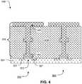
- FIG. 4illustrates a structure 400 formed in a first stage.
- the structure 400includes the floating gate structures (e.g. floating gate structure 318) for the chemical sensors 350, 351.
- the structure 400can be formed by depositing a layer of gate dielectric material on the semiconductor substrate 354, and depositing a layer of polysilicon (or other electrically conductive material) on the layer of gate dielectric material.
- the layer of polysilicon and the layer gate dielectric materialcan then be etched using an etch mask to form the gate dielectric elements (e.g. gate dielectric 352) and the lowermost conductive material element of the floating gate structures.
- ion implantationcan then be performed to form the source and drain regions (e.g. source region 321 and a drain region 322) of the chemical sensors.
- a first layer of the dielectric material 319can then be deposited over the lowermost conductive material elements.
- Conductive plugscan then be formed within vias etched in the first layer of dielectric material 319 to contact the lowermost conductive material elements of the floating gate structures.
- a layer of conductive materialcan then be deposited on the first layer of the dielectric material 319 and patterned to form second conductive material elements electrically connected to the conductive plugs. This process can then be repeated multiple times to form the completed floating gate structure 318 shown in FIG. 4 .
- Forming the structure 400 in FIG. 4can also include forming additional elements such as array lines (e.g. row lines, column lines, etc.) for accessing the chemical sensors, additional doped regions in the substrate 354, and other circuitry (e.g. select switches, access circuitry, bias circuitry etc.) used to operate the chemical sensors, depending upon the device and array configuration in which the chemical sensors described herein are implemented.
- the elements of the structuremay for example be manufactured using techniques described in Schultz et al., U.S. Pat. Appl. No. 12/785,667 (now U.S. Patent No.
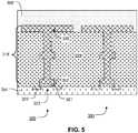
- dielectric material 308 having a given thicknessis deposited on the structure 400 illustrated in FIG. 4 , resulting in the structure illustrated in FIG. 5 .
- the dielectric material 308comprises one or more dielectric layers of dielectric.
- the dielectric material 308may be deposited using a process which results in very small variation in the thickness across the array.
- the dielectric material 308may comprise silicon oxide and be deposited using high density plasma (HDP) deposition.
- HDPhigh density plasma
- Various other techniquesmay be used, such as sputtering, reactive sputtering, atomic layer deposition (ALD), low pressure chemical vapor deposition (LPCVD), plasma enhanced chemical vapor deposition (PECVD), metal organic chemical vapor deposition (MOCVD), etc.
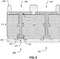
- the dielectric material 308 of the structure in FIG. 5is etched to form cavities 600, 602 extending to the upper surfaces of the floating gate structures of the chemical sensors 350, 351, resulting in the structure illustrated in FIG. 6 .
- the cavities 600, 602may for example be formed by using a lithographic process to pattern a layer of photoresist on the dielectric material 308 to define the locations of the cavities 600, 602, and then anisotropically etching the dielectric material 308 using the patterned photoreist as an etch mask.
- the anisotropic etching of the dielectric material 308may for example be a dry etch process, such as a fluorine based Reactive Ion Etching (RIE) process.
- dielectric material 310is formed on the structure illustrated in FIG. 6 , resulting in the structure illustrated in FIG. 7 .
- the dielectric material 310may comprise one or more layers of deposited dielectric material, such as silicon dioxide or silicon nitride.
- the conductive material 900comprises one or more layers of electrically conductive material.
- the conductive material 900may be a layer of titanium nitride, or a layer of titanium.
- other and/or additional conductive materialsmay be used, such as those described above with reference to the conductive element 370.
- more than one layer of conductive materialmay be deposited.
- the conductive material 900may be deposited using various techniques, such as sputtering, reactive sputtering, atomic layer deposition (ALD), low pressure chemical vapor deposition (LPCVD), plasma enhanced chemical vapor deposition (PECVD), metal organic chemical vapor deposition (MOCVD), etc.
- ALDatomic layer deposition
- LPCVDlow pressure chemical vapor deposition
- PECVDplasma enhanced chemical vapor deposition
- MOCVDmetal organic chemical vapor deposition
- material 1000is formed on the structure illustrated in FIG. 9 , resulting in the structure illustrated in FIG. 10 .
- the material 1000may comprise one or more layers of deposited dielectric material, such as silicon dioxide or silicon nitride.
- material 1000may comprise photoresist.
- a partial etch of material 1000 and conductive material 900is performed such that distance 309 of dielectric material 310 is revealed (that is, distance 309 of sidewall 303 is exposed), resulting in the structure illustrated in FIG. 11 .
- Material 1000 and electrically conductive material 900may be etched together or separately depending on the process and/or material(s) used.
- a partial etchmay be performed using at least one of an O2 resist etch, Ar sputter breakthrough etch, and Hydrogen Bromide Titanium etch.
- material 1000is etched to form openings defining reaction regions 301, 302 extending to the conductive element 370, 900, resulting in the structure illustrated in FIG. 12 .
- residual photoresistmay need to be cleaned from the opening using techniques known to those skilled in the art, for example, O2 plasma ash.
- FIG. 13illustrates a cross-sectional view of two representative chemical sensors and their corresponding reaction regions according to a second embodiment.
- the structure of the two representative chemical sensors illustrated in FIG. 13differs in one aspect from the two representative chemical sensors illustrated in FIG. 3 in that FIG. 13 includes vias over sensor plates 320 on top of which the microwells/nanowells are built. Accordingly, fabrication for the structure in FIG. 3 is different from fabrication of FIG. 13 , as is explained in greater detail below.
- FIGS. 14-25illustrate stages in a manufacturing process for forming an array of chemical devices and corresponding well structures according to an exemplary embodiment.
- FIG. 14illustrates a structure 1400 including the floating gate structures (e.g. floating gate structure 318) for the chemical devices 350, 351.
- the structure 1400can be formed in accordance with the structure 400 described in detail above with reference to FIG. 4 .
- a dielectric material 1503may be formed on the sensor plate 320 of the field effect transistor of the chemical device 350.
- FIG. 16the dielectric material 1503 of the structure 1500 in FIG.
- openings 1618, 1620are etched to form openings 1618, 1620 (for vias) extending to the upper surfaces of the floating gate structures of the chemical devices 350, 351, resulting in the structure 1600 illustrated in FIG. 16 .
- the openings 1618, 1620may, for example, be formed by using a lithographic process to pattern a layer of photoresist on the dielectric material 1503 to define the locations of the openings 1618, 1620, and then anisotropically etching the dielectric material 1503 using the patterned photoreist as an etch mask.
- the anisotropic etching of the dielectric material 1503may, for example, be a dry etch process, such as a fluorine based Reactive Ion Etching (RIE) process.
- RIEfluorine based Reactive Ion Etching
- the openings 1618, 1620are separated by a distance 1630 and the openings 1618, 1620 are of a suitable dimension for a via.
- the separation distance 1630may be a minimum feature size for the process (e.g. a lithographic process) used to form the openings 1618, 1620. In such a case, the distance 1630 may be significantly more than the width 1620.
- a layer of conductive material 1704is deposited on the structure 1600 illustrated in FIG. 16 , resulting in the structure 1700 illustrated in FIG. 17 .
- Conductive material 1704may be referred to as a conductive liner.
- the conductive material 1704may comprise one or more layers of electrically conductive material.
- the conductive material 1704may be a layer of titanium nitride, or a layer of titanium. Alternatively, other and/or additional conductive materials may be used, such as those described above with reference to the electrically conductive element. In addition, more than one layer of conductive material may be deposited.
- the conductive material 1704may be deposited using various techniques, such as sputtering, reactive sputtering, atomic layer deposition (ALD), low pressure chemical vapor deposition (LPCVD), plasma enhanced chemical vapor deposition (PECVD), metal organic chemical vapor deposition (MOCVD), etc.
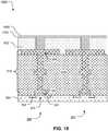
- a layer of conductive material 1805such as tungsten, for example, is deposited on the structure 1700 illustrated in FIG. 17 , resulting in the structure 1800 illustrated in FIG. 18 .
- the conductive material 1805may be deposited using various techniques, such as sputtering, reactive sputtering, atomic layer deposition (ALD), low pressure chemical vapor deposition (LPCVD), plasma enhanced chemical vapor deposition (PECVD), metal organic chemical vapor deposition (MOCVD), etc. or any other suitable techniques.
- conductive material 1704 and conductive material 1805are planarized using a Chemical Mechanical Planarization (CMP) process, for example, resulting in the structure 1900 illustrated in FIG. 19 .
- CMPChemical Mechanical Planarization
- a via barrier linermay be formed on the planarized conductive material 1704 and conductive material 1805.
- the via barrier linermay comprise titanium nitride.
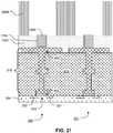
- dielectric material 2006is formed on the structure illustrated in FIG. 19 , resulting in the structure illustrated in FIG. 20 .
- the dielectric material 2006may comprise one or more layers of deposited dielectric material, such as silicon dioxide or silicon nitride.
- dielectric material 2006is etched to form openings extending to planarized conductive material 1704 and conductive material 1805 and dielectric material 1503, resulting in the structure illustrated in FIG. 21 .
- Dielectric material 1503may be partially etched when the openings are formed such that conductive material 1704 and conductive material 1805 are raised above dielectric material 1503 and protrude into the opening, as seen in the illustrated embodiment.
- a conformal layer of conductive material 2200is deposited on the structure illustrated in FIG.
- the conductive material 2200comprises one or more layers of electrically conductive material.
- the conductive material 2200may be a layer of titanium nitride, or a layer of titanium.
- other and/or additional conductive materialsmay be used, such as those described above with reference to the conductive element 370.
- more than one layer of conductive materialmay be deposited.
- the conductive material 2200may be deposited using various techniques, such as sputtering, reactive sputtering, atomic layer deposition (ALD), low pressure chemical vapor deposition (LPCVD), plasma enhanced chemical vapor deposition (PECVD), metal organic chemical vapor deposition (MOCVD), etc.
- material 2300is formed on the structure illustrated in FIG. 22 , resulting in the structure illustrated in FIG. 23 .
- the material 2300may comprise one or more layers of deposited dielectric material, such as silicon dioxide or silicon nitride.
- material 2300may comprise photoresist.
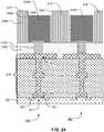
- a partial etch of material 2300 and conductive material 2200is performed such that distance 1309 of dielectric material 310 is revealed (that is, distance 309 of sidewall 1303 is exposed), resulting in the structure illustrated in FIG. 24 .
- Material 2300 and conductive material 2200may be etched together or separately depending on the process and/or material(s) used.
- a partial etchmay be performed using at least one of an O2 resist etch, Ar sputter breakthrough etch, and Hydrogen Bromide Titanium etch.
- material 2300is etched to form openings defining reaction regions 301, 302 extending to the conductive elements 370, 2200, resulting in the structure illustrated in FIG. 25 .
- residual photoresistmay need to be cleaned from the opening using techniques known to those skilled in the art, for example, O2 plasma ash.
Landscapes
- Chemical & Material Sciences (AREA)
- Health & Medical Sciences (AREA)
- Life Sciences & Earth Sciences (AREA)
- Physics & Mathematics (AREA)
- General Health & Medical Sciences (AREA)
- Microelectronics & Electronic Packaging (AREA)
- Engineering & Computer Science (AREA)
- Chemical Kinetics & Catalysis (AREA)
- Analytical Chemistry (AREA)
- Molecular Biology (AREA)
- Electrochemistry (AREA)
- Biochemistry (AREA)
- General Physics & Mathematics (AREA)
- Immunology (AREA)
- Pathology (AREA)
- Computer Hardware Design (AREA)
- Fluid Mechanics (AREA)
- Dispersion Chemistry (AREA)
- Hematology (AREA)
- Clinical Laboratory Science (AREA)
- Investigating Or Analyzing Materials By The Use Of Electric Means (AREA)
- Apparatus Associated With Microorganisms And Enzymes (AREA)
Description
- This application claims priority to
U.S. Provisional Application No. 61/900,907 filed November 6, 2013 61/790,866 filed March 15, 2013 - The present disclosure relates to sensors for chemical analysis, and to methods for manufacturing such sensors.
- A variety of types of chemical sensors have been used in the detection of chemical processes. One type is a chemically-sensitive field effect transistor (chemFET). A chemFET includes a source and a drain separated by a channel region, and a chemically sensitive area coupled to the channel region. The operation of the chemFET is based on the modulation of channel conductance, caused by changes in charge at the sensitive area due to a chemical reaction occurring nearby. The modulation of the channel conductance changes the threshold voltage of the chemFET, which can be measured to detect and/or determine characteristics of the chemical reaction. The threshold voltage may for example be measured by applying appropriate bias voltages to the source and drain, and measuring a resulting current flowing through the chemFET. As another example, the threshold voltage may be measured by driving a known current through the chemFET, and measuring a resulting voltage at the source or drain.
- An ion-sensitive field effect transistor (ISFET) is a type of chemFET that includes an ion-sensitive layer at the sensitive area. The presence of ions in an analyte solution alters the surface potential at the interface between the ion-sensitive layer and the analyte solution, due to the protonation or deprotonation of surface charge groups caused by the ions present in the analyte solution. The change in surface potential at the sensitive area of the ISFET affects the threshold voltage of the device, which can be measured to indicate the presence and/or concentration of ions within the solution. Arrays of ISFETs may be used for monitoring chemical reactions, such as DNA sequencing reactions, based on the detection of ions present, generated, or used during the reactions. See, for example,
Rothberg et al., U.S. Pat. Appl. No. 12/002,291 (nowU.S. Patent No. 7,948,015), filed December 14, 2009 , based on U.S. Prov. Pat. Appl. Nos.60/956,324, filed August 16, 2007 60/968,748, filed July 10, 2007 60/870,073, filed December 14, 2006 - An issue that arises in the operation of large scale chemical sensor arrays is the susceptibility of the sensor output signals to noise. Specifically, the noise affects the accuracy of the downstream signal processing used to determine the characteristics of the chemical and/or biological process being detected by the sensors. In addition, chemical sensor performance variation across the array results in undesirable differences in the sensor output signals, which further complicates the downstream signal processing. It is therefore desirable to provide devices including low noise chemical sensors, and methods for manufacturing such devices.
- In one embodiment, a chemical sensor is described. The chemical sensor includes a chemically-sensitive field effect transistor including a floating gate conductor having an upper surface; a material defining an opening extending to the upper surface of the floating gate conductor, the material comprising a first dielectric underlying a second dielectric; and a conductive element contacting the upper surface of the floating gate conductor and extending a distance along a sidewall of the opening, wherein the conductive element extends along the sidewall between 5% of the sidewall and 85% of the sidewall . In an exemplary embodiment, the opening of the chemical sensor may include a lower portion within the first dielectric, and an upper portion within the second dielectric. In another embodiment, a width of the lower portion of the opening is substantially the same as a width of the upper portion. In yet another embodiment, the conductive element is conformal with a shape of the opening. In one embodiment, the conductive element extends to an upper surface of the second dielectric. In an exemplary embodiment, the conductive element includes an inner surface defining a lower portion of a reaction region for the chemical sensor, and the second dielectric includes an inner surface defining an upper portion of the opening. In an exemplary embodiment, the conductive element comprises an electrically conductive material, and an inner surface of the conductive element includes an oxide of the electrically conductive material. In another embodiment, a sensing surface of the chemical sensor includes an inner surface of the conductive element. In yet another embodiment, the chemically-sensitive field effect transistor generates a sensor signal in response to a chemical reaction occurring proximate to the conductive element. In one embodiment, the floating gate conductor comprises a plurality of conductors electrically coupled to one another and separated by dielectric layers, and the floating gate conductor is an uppermost conductor in the plurality of conductors.
- In another embodiment, a method for manufacturing a chemical sensor is described. The method includes forming a chemically-sensitive field effect transistor including a floating gate conductor having an upper surface; forming a material defining an opening extending to the upper surface of the floating gate conductor, the material comprising a first dielectric underlying a second dielectric; and forming a conductive element contacting the upper surface of the floating gate conductor and extending a distance along a sidewall of the opening, wherein the conductive element extends along the sidewall between 5% of the sidewall and 85% of the sidewall . In an exemplary embodiment, forming the material and forming the conductive element may include forming the first dielectric on the floating gate conductor, the first dielectric defining a cavity extending to the upper surface of the floating gate conductor; forming the second dielectric thereon; etching the second dielectric to expose the conductive element, thereby defining an opening; and forming the conductive element within the opening. According to another embodiment, forming the conductive element within the opening may include depositing a conductive material within the opening and on an upper surface of the first dielectric; and removing at least a portion of the conductive material from the upper surface of the second dielectric. In yet another embodiment, removing at least the portion of the conductive material may comprises depositing a layer of photoresist within the opening; and removing at least a portion of the conductive material together with the photoresist from the upper surface of the second dielectric. In one embodiment, the conductive material comprises titanium. In an exemplary embodiment, the opening is a nanowell. In an exemplary embodiment, the forming a conductive element includes depositing a conductive material conformally within the opening. In another embodiment, the conductive element includes an inner surface defining a lower portion of a reaction region for the chemical sensor, and the second dielectric includes an inner surface defining an upper portion of the opening.
- Particular aspects of one embodiment of the subject matter described in this specification are set forth in the drawings and the description below. Other features, aspects, and advantages of the subject matter will become apparent from the description, the drawings, and the claims.
FIG. 1 illustrates a block diagram of components of a system for nucleic acid sequencing according to an exemplary embodiment.FIG. 2 illustrates a cross-sectional view of a portion of the integrated circuit device and flow cell according to an exemplary embodiment.FIG. 3 illustrates a cross-sectional view of two representative chemical sensors and their corresponding reaction regions according to a first embodiment.FIGS. 4 to 12 illustrate stages in a manufacturing process for forming an array of chemical sensors and corresponding reaction regions according to a first embodiment.FIGS. 13 to 25 illustrate stages in a manufacturing process for forming an array of chemical sensors and corresponding reaction regions according to a second embodiment.- A chemical detection device is described that includes low noise chemical sensors, such as chemically-sensitive field effect transistors (chemFETs), for detecting chemical reactions within overlying, operationally associated reaction regions. Reducing the plan or top view area (or footprint) of individual chemical sensors and the overlying reaction regions allows for higher density devices. However, as the dimensions of the chemical sensors are reduced, Applicants have found that a corresponding reduction in the sensing surface area of the sensors can significantly impact performance. For example, for chemical sensors having sensing surfaces defined at the bottom of the reaction regions, reducing the plan view dimensions (e.g. the width or diameter) of the reaction regions results in a similar reduction in the sensing surface areas. Applicants have found that as the sensing surface area is reduced to technology limits, fluidic noise due to the random fluctuation of charge on the sensing surface contributes to an increasing proportion of the total variation in sensing surface potential. This can significantly reduce the signal-to-noise ratio (SNR) of the sensor output signal, which affects the accuracy of the downstream signal processing used to determine the characteristics of the chemical and/or biological process being detected by the sensor.
- Chemical sensors described herein have sensing surface areas which are not limited to a two-dimensional area at the bottom of the reaction regions. In embodiments described herein, the sensing surface of the chemical sensor includes a generally horizontal portion along the bottom surface of the reaction region, as well as a generally vertical portion extending along a sidewall of an opening containing the reaction region. The distance that the generally vertical portion extends along the sidewall is defined by the thickness of a dielectric material that forms a lower portion of the opening. The dielectric material can be deposited using a process (e.g. thin film deposition) which results in very small thickness variation across the array. In doing so, the sensor surface areas of the chemical sensors can be very well controlled, resulting in uniform chemical sensor performance across the array and thus simplifying the downstream signal processing. By extending the sensing surface in the generally vertical direction, the chemical sensor can have a small footprint, while also having a sufficiently large sensing surface area to avoid the noise issues associated with small sensing surfaces. The footprint of a chemical sensor is determined in part by the width (e.g. diameter) of the overlying reaction region and can be made small, allowing for a high density array. In addition, because the sensing surface extends a controlled distance up the sidewall, the sensing surface area can be relatively large. As a result, low noise chemical sensors can be provided in a high density array, such that the characteristics of reactions can be accurately dctcctcd.
FIG. 1 illustrates a block diagram of components of a system for nucleic acid sequencing according to an exemplary embodiment. The components include aflow cell 101 on anintegrated circuit device 100, areference electrode 108, a plurality ofreagents 114 for sequencing, avalve block 116, awash solution 110, avalve 112, afluidics controller 118,lines 120/122/126,passages 104/109/111, awaste container 106, anarray controller 124, and auser interface 128. Theintegrated circuit device 100 includes amicrowell array 107 overlying a sensor array that includes chemical sensors as described herein. Theflow cell 101 includes aninlet 102, anoutlet 103, and aflow chamber 105 defining a flow path for thereagents 114 over themicrowell array 107. Thereference electrode 108 may be of any suitable type or shape, including a concentric cylinder with a fluid passage or a wire inserted into a lumen ofpassage 111. Thereagents 114 may be driven through the fluid pathways, valves, and flowcell 101 by pumps, gas pressure, vacuum, or other suitable methods, and may be discarded into thewaste container 106 after exiting theoutlet 103 of theflow cell 101. Thefluidics controller 118 may control driving forces for thereagents 114 and the operation ofvalve 112 and valve block 116 with suitable software.- The
microwell array 107 includes reaction regions, also referred to herein as microwells, which are operationally associated with corresponding chemical sensors in the sensor array. For example, each reaction region may be coupled to a chemical sensor suitable for detecting an analyte or reaction property of interest within that reaction region. Themicrowell array 107 may be integrated in theintegrated circuit device 100, so that themicrowell array 107 and the sensor array are part of a single device or chip. Theflow cell 101 may have a variety of configurations for controlling the path and flow rate ofreagents 114 over themicrowell array 107. Thearray controller 124 provides bias voltages and timing and control signals to theintegrated circuit device 100 for reading the chemical sensors of the sensor array. Thearray controller 124 also provides a reference bias voltage to thereference electrode 108 to bias thereagents 114 flowing over themicrowell array 107. - During an experiment, the
array controller 124 collects and processes output signals from the chemical sensors of the sensor array through output ports on theintegrated circuit device 100 viabus 127. Thearray controller 124 may be a computer or other computing means. Thearray controller 124 may include memory for storage of data and software applications, a processor for accessing data and executing applications, and components that facilitate communication with the various components of the system inFIG. 1 . In the illustrated embodiment, thearray controller 124 is external to theintegrated circuit device 100. In some alternative embodiments, some or all of the functions performed by thearray controller 124 are carried out by a controller or other data processor on theintegrated circuit device 100. The values of the output signals from the chemical sensors indicate physical and/or chemical parameters of one or more reactions taking place in the corresponding reaction regions in themicrowell array 107. For example, in an exemplary embodiment, the values of the output signals may be processed using the techniques disclosed inRearick et al., U.S. Pat. Appl. No. 13/339,846, filed December 29, 2011 61/428,743, filed December 30, 2010 61/429,328, filed January 3, 2011 U.S. Pat. Appl. No. 13/339,753, filed December 29, 2011 61/428,097, filed December 29, 2010 user interface 128 may display information about theflow cell 101 and the output signals received from chemical sensors in the sensor array on theintegrated circuit device 100. Theuser interface 128 may also display instrument settings and controls, and allow a user to enter or set instrument settings and controls. - The
fluidics controller 118 may control delivery of theindividual reagents 114 to theflow cell 101 andintegrated circuit device 100 in a predetermined sequence, for predetermined durations, at predetermined flow rates. Thearray controller 124 can then collect and analyze the output signals of the chemical sensors indicating chemical reactions occurring in response to the delivery of thereagents 114. During the experiment, the system may also monitor and control the temperature of theintegrated circuit device 100, so that reactions take place and measurements are made at a known predetermined temperature. - The system may be configured to let a single fluid or reagent contact the
reference electrode 108 throughout an entire multi-step reaction during operation. Thevalve 112 may be shut to prevent anywash solution 110 from flowing intopassage 109 as thereagents 114 are flowing. Although the flow of wash solution may be stopped, there may still be uninterrupted fluid and electrical communication between thereference electrode 108,passage 109, and themicrowell array 107. The distance between thereference electrode 108 and the junction betweenpassages reference electrode 108. In an exemplary embodiment, thewash solution 110 may be selected as being in continuous contact with thereference electrode 108, which may be especially useful for multi-step reactions using frequent wash steps. FIG. 2 illustrates cross-sectional and expanded views of a portion of theintegrated circuit device 100 and flowcell 101. Theintegrated circuit device 100 includes themicrowell array 107 of reaction regions operationally associated withsensor array 205. During operation, theflow chamber 105 of theflow cell 101 confines areagent flow 208 of delivered reagents across open ends of the reaction regions in themicrowell array 107. The volume, shape, aspect ratio (such as base width-to-well depth ratio), and other dimensional characteristics of the reaction regions may be selected based on the nature of the reaction taking place, as well as the reagents, byproducts, or labeling techniques (if any) that are employed. The chemical sensors of thesensor array 205 are responsive to (and generate output signals related to) chemical reactions within associated reaction regions in themicrowell array 107 to detect an analyte or reaction property of interest. The chemical sensors of thesensor array 205 may for example be chemically sensitive field-effect transistors (chemFETs), such as ion-sensitive field effect transistors (ISFETs). Examples of chemical sensors and array configurations that may be used in embodiments are described inSchultz et al., U.S. Pat. Appl. No. 12/785,667 (nowU.S. Patent No. 8,546,128), filed May 24, 2010 , titled "Fluidics System for Sequential Delivery of Reagents"; Rotherberg et al.,U.S. Pat. Appl. No. 12/721,458 (nowU.S. Patent No. 8,306,757), filed March 10, 2010 , titled "Methods and Apparatus for Measuring Analytes Using Large Scale FET Arrays"; Rotherberg et al.,U.S. Pat. Appl. No. 12/475,311, filed May 29, 2009 U.S. Pat. Appl. No. 12/474,897, filed May 29, 2009 U.S. Pat. Appl. No. 12/002,781, filed December 17, 2007 , titled "Methods and Apparatus for Measuring Analytes Using Large Scale FET Arrays"; andU.S. Pat. Appl. No. 12/474,897 (nowU.S. Patent No. 7,575,865) filed August 1, 2005 , titled "Methods of Amplifying and Sequencing Nucleic Acids.FIG. 3 illustrates a cross-sectional view of two representative chemical sensors and their corresponding reaction regions according to a first embodiment. InFIG. 3 , twochemical sensors Chemical sensor 350 is coupled tocorresponding reaction region 301, andchemical sensor 351 is coupled tocorresponding reaction region 302.Chemical sensor 350 is representative of the chemical sensors in the sensor array. In the illustrated example, thechemical sensor 350 is a chemically-sensitive field effect transistor (chemFET), more specifically an ion-sensitive field effect transistor (ISFET) in this example. Thechemical sensor 350 includes a floatinggate structure 318 having asensor plate 320 coupled to thereaction region 301 by an electricallyconductive element 370. As can be seen inFig. 3 , thesensor plate 320 is the uppermost floating gate conductor in the floatinggate structure 318. In the illustrated example, the floatinggate structure 318 includes multiple patterned layers of conductive material within layers ofdielectric material 319.- The
chemical sensor 350 also includes asource region 321 and adrain region 322 within asemiconductor substrate 354. Thesource region 321 and thedrain region 322 comprise doped semiconductor material have a conductivity type different from the conductivity type of thesubstrate 354. For example, thesource region 321 and thedrain region 322 may comprise doped P-type semiconductor material, and the substrate may comprise doped N-type semiconductor material.Channel region 323 separates thesource region 321 and thedrain region 322. The floatinggate structure 318 overlies thechannel region 323, and is separated from thesubstrate 354 by agate dielectric 352. Thegate dielectric 352 may be for example silicon dioxide. Alternatively, other dielectrics may be used for thegate dielectric 352. - As shown in
FIG. 3 , thereaction region 301 is within an opening having asidewall 303 extending throughdielectric materials sensor plate 320. Each of thedielectric materials lower portion 314 withindielectric material 308 and proximate to thesensor plate 320. The opening also includes anupper portion 315 within thedielectric material 310 and extending from thelower portion 314 to the upper surface of thedielectric material 310. In the illustrated embodiment, the width of theupper portion 315 of the opening is substantially the same as the width of thelower portion 314 of the opening. However, depending on the material(s) and/or etch process used to create the opening, the width of theupper portion 315 of the opening may be greater than the width of thelower portion 314 of the opening, or vice versa. The opening may for example have a circular cross-section. Alternatively, the opening may be non-circular. For example, the cross-section may be square, rectangular, hexagonal, or irregularly shaped. The dimensions of the openings, and their pitch, can vary from embodiment to embodiment. In some embodiments, the openings can have a characteristic diameter, defined as the square root of 4 times the plan view cross-sectional area (A) divided by Pi (e.g., sqrt(4∗A/π)), of not greater than 5 micrometers, such as not greater than 3.5 micrometers, not greater than 2.0 micrometers, not greater than 1.6 micrometers, not greater than 1.0 micrometers, not greater than 0.8 micrometers, not greater than 0.6 micrometers, not greater than 0.4 micrometers, not greater than 0.2 micrometers or even not greater than 0.1 micrometers. - The
lower portion 314 of the opening includes the electricallyconductive element 370 on thesidewall 303 of thedielectric material 310. In the illustrated embodiment, theinner surface 371 of the electricallyconductive element 370 defines a lower segment of thereaction region 301. That is, there is no intervening deposited material layer between theinner surface 371 of the electricallyconductive element 370 and thereaction region 301 for thechemical sensor 350. As a result of this structure, theinner surface 371 of the electricallyconductive element 370 is conformal to the opening and acts as the sensing surface for thechemical sensor 350. It should be understood by those skilled in the art that precise shape and dimension of the electricallyconductive element 370, as with all other materials illustrated in the figures, is process dependant. - In the illustrated embodiment, the electrically
conductive element 370 is a conformal layer of material within thelower portion 314 of the opening, such that the electricallyconductive element 370 extends across the upper surface of thesensor plate 320. In the illustrated embodiment, the electricallyconductive element 370 extends beyond thelower portion 314 of the opening and into theupper portion 315 of the opening. The inner surface of thedielectric material 310 defines an upper segment of thereaction region 301. According to the claimed invention, the conductive element extends along the sidewall between 5% of the sidewall and 85% of the sidewall, in examples outside the scope of the appended claims, theconductive element 370 may for example extend along at least 5% of thesidewall 303, at least 10%, at least 25%, at least 50%, at least 75%, or at least 85% of thesidewall 303, or even extend along 99% of thesidewall 303. The conformalinner surface 371 of the electricallyconductive element 370 allows thechemical sensor 350 to have a small plan view area, while also having a sufficiently large surface area to avoid the noise issues associated with small sensing surfaces. The plan view area of thechemical sensor 350 is determined in part by the width (or diameter) of thereaction region 301 and can be made small, allowing for a high density array. In addition, because the sensing surface extends up thesidewall 303, the sensing surface area depends upon the distance of this extension and the circumference of thereaction region 301, and can be relatively large. As a result, lownoise chemical sensors - During manufacturing and/or operation of the device, a thin oxide of the material of the electrically
conductive element 370 may be grown which acts as a sensing material (e.g. an ion-sensitive sensing material) for thechemical sensor 350. Whether an oxide is formed depends on the conductive material, the manufacturing processes performed, and the conditions under which the device is operated. For example, in one embodiment the electricallyconductive element 370 may be titanium nitride, and titanium oxide or titanium oxynitride may be grown on theinner surface 371 of theconductive element 370 during manufacturing and/or during exposure to solutions during use. In the illustrated example, the electricallyconductive element 370 is shown as a single layer of material. More generally, the electricallyconductive element 370 may comprise one or more layers of a variety of electrically conductive materials, such as metals or ceramics, depending upon the embodiment. The conductive material can be for example a metallic material or alloy thereof, or can be a ceramic material, or a combination thereof. An exemplary metallic material includes one of aluminum, copper, nickel, titanium, silver, gold, platinum, hafnium, lanthanum, tantalum, tungsten, iridium, zirconium, palladium, or a combination thereof. An exemplary ceramic material includes one of titanium nitride, titanium aluminum nitride, titanium oxynitride, tantalum nitride or a combination thereof. In some alternative embodiments, an additional conformal sensing material (not shown) is deposited on theconductive element 370 and within the openings. The sensing material may comprise one or more of a variety of different materials to facilitate sensitivity to particular ions. For example, silicon nitride or silicon oxynitride, as well as metal oxides such as silicon oxide, aluminum or tantalum oxides, generally provide sensitivity to hydrogen ions, whereas sensing materials comprising polyvinyl chloride containing valinomycin provide sensitivity to potassium ions. Materials sensitive to other ions such as sodium, silver, iron, bromine, iodine, calcium, and nitrate may also be used, depending upon the embodiment. - In operation, reactants, wash solutions, and other reagents may move in and out of the
reaction region 301 by adiffusion mechanism 340. Thechemical sensor 350 is responsive to (and generates an output signal related to) the amount of charge 324 proximate to theconductive element 370. The presence of charge 324 in an analyte solution alters the surface potential at the interface between theconductive element 370 and the analyte solution within thereaction region 301. Changes in the charge 324 cause changes in the voltage on the floatinggate structure 318, which in turn changes in the threshold voltage of the transistor. This change in threshold voltage can be measured by measuring the current in thechannel region 323 between thesource region 321 and adrain region 322. As a result, thechemical sensor 350 can be used directly to provide a current-based output signal on an array line connected to thesource region 321 or drainregion 322, or indirectly with additional circuitry to provide a voltage-based output signal. Because the charge 324 may be more highly concentrated near the bottom of thereaction region 301, the distance that theconductive element 370 extends up thesidewall 303 of the opening is a tradeoff between the amplitude of the desired signal detected in response to the charge 324, and the fluidic noise due to random fluctuation of charge between theconductive element 370 and the analyte solution. Increasing the distance that theconductive element 370 extends up thesidewall 303 increases the fluidic interface area for thechemical sensor 350, which acts to reduce the fluidic noise. However, due to the diffusion of charge 324 out of thereaction region 301, the concentration of charge 324 decreases with distance from the bottom of thereaction region 301. As a result, upper sidewall segments of theconductive element 370 detect portions of the signal from areas having lower charge concentration, which can reduce the overall amplitude of the desired signal detected by thesensor 350. In contrast, decreasing the distance theconductive element 370 extends up thesidewall 303 reduces the sensing surface area and thus increases the fluidic noise, but also increases the overall amplitude of the desired signal detected by thesensor 350. - For a very small sensing surface area, Applicants have found that the fluidic noise changes as a function of the sensing surface area differently than the amplitude of the desired signal. Because the SNR of the sensor output signal is the ratio of these two quantities, there is an optimal distance the
conductive element 370 extends along thesidewall 303 at which SNR is maximum. The optimal distance can vary from embodiment to embodiment depending on the material characteristics of theconductive element 370 and thedielectric material 310, the volume, shape, aspect ratio (such as base width-to-well depth ratio), and other dimensional characteristics of the reaction regions, the nature of the reaction taking place, as well as the reagents, byproducts, or labeling techniques (if any) that are employed. The optimal distance may for example be determined empirically. - As described in more detail below with respect to
FIGS. 4 to 12 , the distance theconductive element 370 extends along thesidewall 303 is defined by the etch time of the deposited layer, for example. Thedielectric material 310 and electricallyconductive element 370 can be etched using a timed etch process, for example, which results in selectivity of distance 309 (e.g. thedistance dielectric material 310 extends beyond electrically conductive element 370). In doing so, the sensor surface areas of the chemical sensors can be controlled, resulting in uniform chemical sensor performance across the array and simplifying the downstream signal processing. - In an embodiment, reactions carried out in the
reaction region 301 can be analytical reactions to identify or determine characteristics or properties of an analyte of interest. Such reactions can generate directly or indirectly byproducts that affect the amount of charge adjacent to the electricallyconductive element 370. If such byproducts arc produced in small amounts or rapidly decay or react with other constituents, multiple copies of the same analyte may be analyzed in thereaction region 301 at the same time in order to increase the output signal generated. In an embodiment, multiple copies of an analyte may be attached to asolid phase support 312, as shown inFIG. 3 , either before or after deposition into thereaction region 301. Thesolid phase support 312 may be microparticles, nanoparticles, beads, solid or porous gels, or the like. For simplicity and ease of explanation,solid phase support 312 is also referred herein as a particle. For a nucleic acid analyte, multiple, connected copies may be made by rolling circle amplification (RCA), exponential RCA, Recombinase Polymerase Amplification (RPA), Polymerase Chain Reaction amplification (PCR), emulsion PCR amplification, or like techniques, to produce an amplicon without the need of a solid support. - In various examples, which are not covered by the appended claims, the methods, systems, and computer readable media described herein may advantageously be used to process and/or analyze data and signals obtained from electronic or charged-based nucleic acid sequencing. In electronic or charged-based sequencing (such as, pH-based sequencing), a nucleotide incorporation event may be determined by detecting ions (e.g., hydrogen ions) that are generated as natural by-products of polymerase-catalyzed nucleotide extension reactions. This may be used to sequence a sample or template nucleic acid, which may be a fragment of a nucleic acid sequence of interest, for example, and which may be directly or indirectly attached as a clonal population to a solid support, such as a particle, microparticle, bead, etc. The sample or template nucleic acid may be operably associated to a primer and polymerase and may be subjected to repeated cycles or "flows" of deoxynucleoside triphosphate ("dNTP") addition (which may be referred to herein as "nucleotide flows" from which nucleotide incorporations may result) and washing. The primer may be annealed to the sample or template so that the primer's 3' end can be extended by a polymerase whenever dNTPs complementary to the next base in the template are added. Then, based on the known sequence of nucleotide flows and on measured output signals of the chemical sensors indicative of ion concentration during each nucleotide flow, the identity of the type, sequence and number of nucleotide(s) associated with a sample nucleic acid present in a reaction region coupled to a chemical sensor can be determined.
FIGS. 4 to 12 illustrate stages in a manufacturing process for forming an array of chemical sensors and corresponding reaction regions according to a first embodiment.FIG. 4 illustrates astructure 400 formed in a first stage. Thestructure 400 includes the floating gate structures (e.g. floating gate structure 318) for thechemical sensors structure 400 can be formed by depositing a layer of gate dielectric material on thesemiconductor substrate 354, and depositing a layer of polysilicon (or other electrically conductive material) on the layer of gate dielectric material. The layer of polysilicon and the layer gate dielectric material can then be etched using an etch mask to form the gate dielectric elements (e.g. gate dielectric 352) and the lowermost conductive material element of the floating gate structures. Following formation of an ion-implantation mask, ion implantation can then be performed to form the source and drain regions (e.g. source region 321 and a drain region 322) of the chemical sensors. A first layer of thedielectric material 319 can then be deposited over the lowermost conductive material elements. Conductive plugs can then be formed within vias etched in the first layer ofdielectric material 319 to contact the lowermost conductive material elements of the floating gate structures. A layer of conductive material can then be deposited on the first layer of thedielectric material 319 and patterned to form second conductive material elements electrically connected to the conductive plugs. This process can then be repeated multiple times to form the completed floatinggate structure 318 shown inFIG. 4 . Alternatively, other and/or additional techniques may be performed to form the structure. Forming thestructure 400 inFIG. 4 can also include forming additional elements such as array lines (e.g. row lines, column lines, etc.) for accessing the chemical sensors, additional doped regions in thesubstrate 354, and other circuitry (e.g. select switches, access circuitry, bias circuitry etc.) used to operate the chemical sensors, depending upon the device and array configuration in which the chemical sensors described herein are implemented. In some embodiments, the elements of the structure may for example be manufactured using techniques described inSchultz et al., U.S. Pat. Appl. No. 12/785,667 (nowU.S. Patent No. 8,546,128), filed May 24, 2010 , titled "Fluidics System for Sequential Delivery of Reagents";Rotherberg et al., U.S. Pat. Appl. No. 12/721,458 (nowU.S. Patent No. 8,306,757), filed March 10, 2010 , titled "Methods and Apparatus for Measuring Analytes Using Large Scale FET Arrays";Rotherberg et al., U.S. Pat. Appl. No. 12/475,311, filed May 29, 2009 Rotherberg et al., U.S. Pat. Appl. No. 12/474,897, filed May 29, 2009 Rotherberg et al., U.S. Pat. Appl. No. 12/002,781, filed December 17, 2007 , titled "Methods and Apparatus for Measuring Analytes Using Large Scale FET Arrays"; andU.S. Pat. Appl. No. 12/474,897 (nowU.S. Patent No. 7,575,865) filed August 1, 2005 , titled "Methods of Amplifying and Sequencing Nucleic Acids'.- Next,
dielectric material 308 having a given thickness is deposited on thestructure 400 illustrated inFIG. 4 , resulting in the structure illustrated inFIG. 5 . Thedielectric material 308 comprises one or more dielectric layers of dielectric. Thedielectric material 308 may be deposited using a process which results in very small variation in the thickness across the array. For example, thedielectric material 308 may comprise silicon oxide and be deposited using high density plasma (HDP) deposition. Various other techniques may be used, such as sputtering, reactive sputtering, atomic layer deposition (ALD), low pressure chemical vapor deposition (LPCVD), plasma enhanced chemical vapor deposition (PECVD), metal organic chemical vapor deposition (MOCVD), etc. Next, thedielectric material 308 of the structure inFIG. 5 is etched to formcavities chemical sensors FIG. 6 . Thecavities dielectric material 308 to define the locations of thecavities dielectric material 308 using the patterned photoreist as an etch mask. The anisotropic etching of thedielectric material 308 may for example be a dry etch process, such as a fluorine based Reactive Ion Etching (RIE) process. Next,dielectric material 310 is formed on the structure illustrated inFIG. 6 , resulting in the structure illustrated inFIG. 7 . Thedielectric material 310 may comprise one or more layers of deposited dielectric material, such as silicon dioxide or silicon nitride. - Next,
dielectric material 310 is etched to form openings definingreaction regions sensor plate 320, resulting in the structure illustrated inFIG. 8 . Next, a conformal layer ofconductive material 900 is deposited on the structure illustrated inFIG. 8 , resulting in the structure illustrated inFIG. 9 . Theconductive material 900 comprises one or more layers of electrically conductive material. For example, theconductive material 900 may be a layer of titanium nitride, or a layer of titanium. Alternatively, other and/or additional conductive materials may be used, such as those described above with reference to theconductive element 370. In addition, more than one layer of conductive material may be deposited. Theconductive material 900 may be deposited using various techniques, such as sputtering, reactive sputtering, atomic layer deposition (ALD), low pressure chemical vapor deposition (LPCVD), plasma enhanced chemical vapor deposition (PECVD), metal organic chemical vapor deposition (MOCVD), etc. - Next,
material 1000 is formed on the structure illustrated inFIG. 9 , resulting in the structure illustrated inFIG. 10 . Thematerial 1000 may comprise one or more layers of deposited dielectric material, such as silicon dioxide or silicon nitride. Alternatively,material 1000 may comprise photoresist. In one embodiment, where thematerial 1000 comprises photoresist, a partial etch ofmaterial 1000 andconductive material 900 is performed such thatdistance 309 ofdielectric material 310 is revealed (that is,distance 309 ofsidewall 303 is exposed), resulting in the structure illustrated inFIG. 11 .Material 1000 and electricallyconductive material 900 may be etched together or separately depending on the process and/or material(s) used. For example, a partial etch may be performed using at least one of an O2 resist etch, Ar sputter breakthrough etch, and Hydrogen Bromide Titanium etch. Next,material 1000 is etched to form openings definingreaction regions conductive element FIG. 12 . In one embodiment, residual photoresist may need to be cleaned from the opening using techniques known to those skilled in the art, for example, O2 plasma ash. FIG. 13 illustrates a cross-sectional view of two representative chemical sensors and their corresponding reaction regions according to a second embodiment. The structure of the two representative chemical sensors illustrated inFIG. 13 differs in one aspect from the two representative chemical sensors illustrated inFIG. 3 in thatFIG. 13 includes vias oversensor plates 320 on top of which the microwells/nanowells are built. Accordingly, fabrication for the structure inFIG. 3 is different from fabrication ofFIG. 13 , as is explained in greater detail below.FIGS. 14-25 illustrate stages in a manufacturing process for forming an array of chemical devices and corresponding well structures according to an exemplary embodiment.FIG. 14 illustrates astructure 1400 including the floating gate structures (e.g. floating gate structure 318) for thechemical devices structure 1400 can be formed in accordance with thestructure 400 described in detail above with reference toFIG. 4 . As illustrated in thestructure 1500 illustrated inFIG. 15 , adielectric material 1503 may be formed on thesensor plate 320 of the field effect transistor of thechemical device 350. Next, as illustrated inFIG. 16 , thedielectric material 1503 of thestructure 1500 inFIG. 15 is etched to formopenings 1618, 1620 (for vias) extending to the upper surfaces of the floating gate structures of thechemical devices structure 1600 illustrated inFIG. 16 . Theopenings dielectric material 1503 to define the locations of theopenings dielectric material 1503 using the patterned photoreist as an etch mask. The anisotropic etching of thedielectric material 1503 may, for example, be a dry etch process, such as a fluorine based Reactive Ion Etching (RIE) process. In the illustrated embodiment, theopenings distance 1630 and theopenings separation distance 1630 may be a minimum feature size for the process (e.g. a lithographic process) used to form theopenings distance 1630 may be significantly more than thewidth 1620. Next, a layer ofconductive material 1704 is deposited on thestructure 1600 illustrated inFIG. 16 , resulting in thestructure 1700 illustrated inFIG. 17 .Conductive material 1704 may be referred to as a conductive liner. Theconductive material 1704 may comprise one or more layers of electrically conductive material. For example, theconductive material 1704 may be a layer of titanium nitride, or a layer of titanium. Alternatively, other and/or additional conductive materials may be used, such as those described above with reference to the electrically conductive element. In addition, more than one layer of conductive material may be deposited. Theconductive material 1704 may be deposited using various techniques, such as sputtering, reactive sputtering, atomic layer deposition (ALD), low pressure chemical vapor deposition (LPCVD), plasma enhanced chemical vapor deposition (PECVD), metal organic chemical vapor deposition (MOCVD), etc.- Next, a layer of
conductive material 1805 such as tungsten, for example, is deposited on thestructure 1700 illustrated inFIG. 17 , resulting in thestructure 1800 illustrated inFIG. 18 . Theconductive material 1805 may be deposited using various techniques, such as sputtering, reactive sputtering, atomic layer deposition (ALD), low pressure chemical vapor deposition (LPCVD), plasma enhanced chemical vapor deposition (PECVD), metal organic chemical vapor deposition (MOCVD), etc. or any other suitable techniques. Next,conductive material 1704 andconductive material 1805 are planarized using a Chemical Mechanical Planarization (CMP) process, for example, resulting in thestructure 1900 illustrated inFIG. 19 . As an optional, additional step, a via barrier liner (not shown) may be formed on the planarizedconductive material 1704 andconductive material 1805. For example, the via barrier liner may comprise titanium nitride. - Next,
dielectric material 2006 is formed on the structure illustrated inFIG. 19 , resulting in the structure illustrated inFIG. 20 . Thedielectric material 2006 may comprise one or more layers of deposited dielectric material, such as silicon dioxide or silicon nitride. Next,dielectric material 2006 is etched to form openings extending to planarizedconductive material 1704 andconductive material 1805 anddielectric material 1503, resulting in the structure illustrated inFIG. 21 .Dielectric material 1503 may be partially etched when the openings are formed such thatconductive material 1704 andconductive material 1805 are raised abovedielectric material 1503 and protrude into the opening, as seen in the illustrated embodiment. Next, a conformal layer ofconductive material 2200 is deposited on the structure illustrated inFIG. 21 , resulting in the structure illustrated inFIG. 22 . Theconductive material 2200 comprises one or more layers of electrically conductive material. For example, theconductive material 2200 may be a layer of titanium nitride, or a layer of titanium. Alternatively, other and/or additional conductive materials may be used, such as those described above with reference to theconductive element 370. In addition, more than one layer of conductive material may be deposited. Theconductive material 2200 may be deposited using various techniques, such as sputtering, reactive sputtering, atomic layer deposition (ALD), low pressure chemical vapor deposition (LPCVD), plasma enhanced chemical vapor deposition (PECVD), metal organic chemical vapor deposition (MOCVD), etc. - Next,
material 2300 is formed on the structure illustrated inFIG. 22 , resulting in the structure illustrated inFIG. 23 . Thematerial 2300 may comprise one or more layers of deposited dielectric material, such as silicon dioxide or silicon nitride. Alternatively,material 2300 may comprise photoresist. In one embodiment, where thematerial 2300 comprises photoresist, a partial etch ofmaterial 2300 andconductive material 2200 is performed such thatdistance 1309 ofdielectric material 310 is revealed (that is,distance 309 ofsidewall 1303 is exposed), resulting in the structure illustrated inFIG. 24 .Material 2300 andconductive material 2200 may be etched together or separately depending on the process and/or material(s) used. For example, a partial etch may be performed using at least one of an O2 resist etch, Ar sputter breakthrough etch, and Hydrogen Bromide Titanium etch. Next,material 2300 is etched to form openings definingreaction regions conductive elements FIG. 25 . In one embodiment, residual photoresist may need to be cleaned from the opening using techniques known to those skilled in the art, for example, O2 plasma ash. - While the present invention is disclosed by reference to the preferred embodiments and examples detailed above, it is to be understood that these examples are intended in an illustrative rather than in a limiting sense. It is contemplated that modifications and combinations will readily occur to those skilled in the art, which modifications and combinations will be within the scope of the following claims. What is claimed is:
Claims (15)
- A chemical sensor (350; 351) comprising:a chemically-sensitive field effect transistor including a floating gate conductor having an upper surface;a material defining an opening extending to the upper surface of the floating gate conductor, the material comprising a first dielectric (308) underlying a second dielectric (310); anda conductive element (370) contacting the upper surface of the floating gate conductor and extending a distance along a sidewall of the opening (308),characterised in that the conductive element (370) extends along the sidewall between 5% of the sidewall and 85% of the sidewall.
- The chemical sensor (350; 351) of claim 1, wherein the opening includes a lower portion within the first dielectric (308), and an upper portion within the second dielectric (310).
- The chemical sensor (350; 351) of claim 2, wherein a width of the lower portion of the opening is substantially the same as a width of the upper portion.
- The chemical sensor (350; 351) of claim 2, wherein the conductive element is conformal with a shape of the opening.
- The chemical sensor (350; 351) of claim 1, wherein the conductive element extends to an upper surface of the second dielectric (310).
- The chemical sensor (350; 351) of claim 1, wherein the conductive element (370) includes an inner surface defining a lower portion of a reaction region (301; 302) for the chemical sensor (350; 351), and the second dielectric (310) includes an inner surface defining an upper portion of the opening.
- The chemical sensor (350; 351) of claim 1, wherein the conductive element (370) comprises an electrically conductive material, and an inner surface of the conductive element (370) includes an oxide of the electrically conductive material.
- The chemical sensor (350; 351) of claim 1, wherein a sensing surface of the chemical sensor (301; 302) includes an inner surface of the conductive element (370).
- The chemical sensor (350; 351) of claim 1, wherein the chemically-sensitive field effect transistor generates a sensor signal in response to a chemical reaction occurring proximate to the conductive element.
- The chemical sensor (350; 351) of claim 1, wherein the floating gate conductor comprises a plurality of conductors electrically coupled to one another and separated by dielectric layers, and the floating gate conductor is an uppermost conductor in the plurality of conductors.
- A method for manufacturing a chemical sensor (350; 351), the method comprising:forming a chemically-sensitive field effect transistor including a floating gate conductor having an upper surface;forming a material defining an opening extending to the upper surface of the floating gate conductor, the material comprising a first dielectric (308) underlying a second dielectric (310); andforming a conductive element (370) contacting the upper surface of the floating gate conductor and extending a distance along a sidewall of the opening,characterised in that the conductive element (370) extends along the sidewall between 5% of the sidewall and 85% of the sidewall.
- The method of claim 11, wherein forming the material and forming the conductive element (370) include:forming the first dielectric (308) on the floating gate conductor, the first dielectric (308) defining a cavity extending to the upper surface of the floating gate conductor;forming the second dielectric (310) thereon;etching the second dielectric (310) to expose the conductive element, thereby defining an opening; andforming the conductive element (370) within the opening.
- The method of claim 12, wherein forming the conductive element (370) within the opening comprises:
depositing a conductive material within the opening and on an upper surface of the first dielectric (308); and removing at least a portion of the conductive material from the upper surface of the second dielectric (310). - The method of claim 13, wherein removing at least the portion of the conductive material comprises:depositing a layer of photoresist within the opening and; andremoving at least a portion of the conductive material together with the photoresist from the upper surface of the second dielectric (310).
- The method of claim 11, wherein the conductive material comprises titanium.
Applications Claiming Priority (3)
| Application Number | Priority Date | Filing Date | Title |
|---|---|---|---|
| US201361790866P | 2013-03-15 | 2013-03-15 | |
| US201361900907P | 2013-11-06 | 2013-11-06 | |
| PCT/US2014/020900WO2014149780A1 (en) | 2013-03-15 | 2014-03-05 | Chemical sensor with consistent sensor surface areas |
Publications (2)
| Publication Number | Publication Date |
|---|---|
| EP2972280A1 EP2972280A1 (en) | 2016-01-20 |
| EP2972280B1true EP2972280B1 (en) | 2021-09-29 |
Family
ID=50349935
Family Applications (1)
| Application Number | Title | Priority Date | Filing Date |
|---|---|---|---|
| EP14712488.7AActiveEP2972280B1 (en) | 2013-03-15 | 2014-03-05 | Chemical sensor with consistent sensor surface areas |
Country Status (5)
| Country | Link |
|---|---|
| US (3) | US20140264472A1 (en) |
| EP (1) | EP2972280B1 (en) |
| JP (2) | JP2016510895A (en) |
| CN (1) | CN105264366B (en) |
| WO (1) | WO2014149780A1 (en) |
Families Citing this family (22)
| Publication number | Priority date | Publication date | Assignee | Title |
|---|---|---|---|---|
| CA2672315A1 (en) | 2006-12-14 | 2008-06-26 | Ion Torrent Systems Incorporated | Methods and apparatus for measuring analytes using large scale fet arrays |
| US8776573B2 (en) | 2009-05-29 | 2014-07-15 | Life Technologies Corporation | Methods and apparatus for measuring analytes |
| JP2013540259A (en) | 2010-06-30 | 2013-10-31 | ライフ テクノロジーズ コーポレーション | Array column integrator |
| WO2012003363A1 (en) | 2010-06-30 | 2012-01-05 | Life Technologies Corporation | Ion-sensing charge-accumulation circuits and methods |
| US11307166B2 (en) | 2010-07-01 | 2022-04-19 | Life Technologies Corporation | Column ADC |
| US9970984B2 (en) | 2011-12-01 | 2018-05-15 | Life Technologies Corporation | Method and apparatus for identifying defects in a chemical sensor array |
| US9841398B2 (en) | 2013-01-08 | 2017-12-12 | Life Technologies Corporation | Methods for manufacturing well structures for low-noise chemical sensors |
| JP6671274B2 (en) | 2013-03-15 | 2020-03-25 | ライフ テクノロジーズ コーポレーション | Chemical device with thin conductive element |
| EP2972280B1 (en)* | 2013-03-15 | 2021-09-29 | Life Technologies Corporation | Chemical sensor with consistent sensor surface areas |
| US10458942B2 (en) | 2013-06-10 | 2019-10-29 | Life Technologies Corporation | Chemical sensor array having multiple sensors per well |
| US9023674B2 (en)* | 2013-09-20 | 2015-05-05 | Taiwan Semiconductor Manufacturing Company, Ltd. | Biosensing well array with protective layer |
| KR102593647B1 (en) | 2014-12-18 | 2023-10-26 | 라이프 테크놀로지스 코포레이션 | High data rate integrated circuit with transmitter configuration |
| US10077472B2 (en) | 2014-12-18 | 2018-09-18 | Life Technologies Corporation | High data rate integrated circuit with power management |
| JP6352843B2 (en)* | 2015-03-24 | 2018-07-04 | 東芝メモリ株式会社 | Semiconductor memory device |
| CN107923869B (en)* | 2015-08-25 | 2021-10-08 | 生命技术公司 | Design of deep microwell and method of making the same |
| CN108291251A (en) | 2015-09-22 | 2018-07-17 | 生命技术公司 | System and method for foranalysis of nucleic acids |
| EP3510388A1 (en)* | 2016-09-09 | 2019-07-17 | Life Technologies Corporation | Chemically-sensitive field-effect transistor with microwell structure and method for producing the same |
| WO2018187511A1 (en)* | 2017-04-04 | 2018-10-11 | Life Technologies Corporation | Method for making a well disposed over a sensor |
| CN107090404B (en)* | 2017-04-21 | 2019-08-13 | 京东方科技集团股份有限公司 | A kind of gene sequencing chip and gene order surveying method, gene sequencing device |
| US11338294B2 (en) | 2017-04-27 | 2022-05-24 | Polybiomics, Inc. | Orthogonal polybiosensing and imaging systems |
| EP3615921A4 (en)* | 2017-04-27 | 2021-04-14 | Polybiomics, Inc. | Orthogonal polybiosensing and imaging systems |
| CN112585459B (en)* | 2018-08-17 | 2024-01-02 | 生命技术公司 | Method of forming an ion sensor |
Family Cites Families (521)
| Publication number | Priority date | Publication date | Assignee | Title |
|---|---|---|---|---|
| US3531258A (en) | 1967-11-16 | 1970-09-29 | Us Health Education & Welfare | Apparatus for the automated synthesis of peptides |
| DE2413703C3 (en) | 1974-03-21 | 1979-01-04 | Max-Planck-Gesellschaft Zur Foerderung Der Wissenschaften E.V., 3400 Goettingen | Valve arrangement for the supply of liquid or gaseous substances to a processing vessel |
| JPS5530312B2 (en) | 1975-01-16 | 1980-08-09 | ||
| US5132418A (en) | 1980-02-29 | 1992-07-21 | University Patents, Inc. | Process for preparing polynucleotides |
| JPS57136158A (en) | 1981-02-17 | 1982-08-23 | Sumitomo Electric Ind Ltd | Ph electrode |
| GB2096824A (en) | 1981-04-09 | 1982-10-20 | Sibbald Alastair | Chemically sensitive field effect transistor |
| EP0065202B1 (en) | 1981-05-15 | 1986-03-12 | Licentia Patent-Verwaltungs-GmbH | Method for measuring ionic concentrations |
| FR2510260A1 (en) | 1981-07-24 | 1983-01-28 | Suisse Fond Rech Microtech | ION-SENSITIVE SEMICONDUCTOR DEVICE |
| US4438354A (en) | 1981-08-14 | 1984-03-20 | American Microsystems, Incorporated | Monolithic programmable gain-integrator stage |
| US4411741A (en) | 1982-01-12 | 1983-10-25 | University Of Utah | Apparatus and method for measuring the concentration of components in fluids |
| US4558845A (en) | 1982-09-22 | 1985-12-17 | Hunkapiller Michael W | Zero dead volume valve |
| NL8302964A (en) | 1983-08-24 | 1985-03-18 | Cordis Europ | DEVICE FOR DETERMINING THE ACTIVITY OF AN ION (PION) IN A LIQUID. |
| NL8303792A (en) | 1983-11-03 | 1985-06-03 | Cordis Europ | Apparatus provided with an measuring circuit based on an ISFET; ISFET SUITABLE FOR USE IN THE MEASURING CIRCUIT AND METHOD FOR MANUFACTURING AN ISFET TO BE USED IN THE MEASURING CIRCUIT |
| JPS60128345A (en) | 1983-12-15 | 1985-07-09 | Olympus Optical Co Ltd | Measuring device for ion concentration |
| US4660063A (en) | 1985-03-18 | 1987-04-21 | General Electric Company | Immersion type ISFET |
| DE3513168A1 (en) | 1985-04-12 | 1986-10-16 | Thomas 8000 München Dandekar | BIOSENSOR CONSISTING OF A SEMICONDUCTOR BASED ON SILICON OR CARBON-BASED (ELECTRONIC PART) AND NUCLEIN BASE (OR. OTHER BIOL. MONOMERS) |
| US4743954A (en) | 1985-06-07 | 1988-05-10 | University Of Utah | Integrated circuit for a chemical-selective sensor with voltage output |
| US4863849A (en) | 1985-07-18 | 1989-09-05 | New York Medical College | Automatable process for sequencing nucleotide |
| EP0213825A3 (en) | 1985-08-22 | 1989-04-26 | Molecular Devices Corporation | Multiple chemically modulated capacitance |
| GB8522785D0 (en) | 1985-09-14 | 1985-10-16 | Emi Plc Thorn | Chemical-sensitive semiconductor device |
| US5140393A (en) | 1985-10-08 | 1992-08-18 | Sharp Kabushiki Kaisha | Sensor device |
| US4822566A (en) | 1985-11-19 | 1989-04-18 | The Johns Hopkins University | Optimized capacitive sensor for chemical analysis and measurement |
| JPS62237349A (en) | 1986-04-08 | 1987-10-17 | Nec Corp | Instrument for measuring distribution of hydrogen ion concentration |
| US4864229A (en) | 1986-05-03 | 1989-09-05 | Integrated Ionics, Inc. | Method and apparatus for testing chemical and ionic sensors |
| US4722830A (en) | 1986-05-05 | 1988-02-02 | General Electric Company | Automated multiple stream analysis system |
| US5082788A (en) | 1986-08-27 | 1992-01-21 | Porton Instruments, Inc. | Method of sequencing peptides and proteins using a valve block assembly |
| US5113870A (en) | 1987-05-01 | 1992-05-19 | Rossenfeld Joel P | Method and apparatus for the analysis, display and classification of event related potentials by interpretation of P3 responses |
| US4927736A (en) | 1987-07-21 | 1990-05-22 | Hoechst Celanese Corporation | Hydroxy polyimides and high temperature positive photoresists therefrom |
| ATE147511T1 (en) | 1988-02-08 | 1997-01-15 | I Stat Corp | METAL OXIDE ELECTRODE |
| US4971903A (en) | 1988-03-25 | 1990-11-20 | Edward Hyman | Pyrophosphate-based method and apparatus for sequencing nucleic acids |
| US4874499A (en) | 1988-05-23 | 1989-10-17 | Massachusetts Institute Of Technology | Electrochemical microsensors and method of making such sensors |
| US5200051A (en) | 1988-11-14 | 1993-04-06 | I-Stat Corporation | Wholly microfabricated biosensors and process for the manufacture and use thereof |
| US4893088A (en) | 1988-11-16 | 1990-01-09 | Harris Corporation | Transimpedance focal plane processor |
| US4990974A (en) | 1989-03-02 | 1991-02-05 | Thunderbird Technologies, Inc. | Fermi threshold field effect transistor |
| JPH02250331A (en) | 1989-03-24 | 1990-10-08 | Hitachi Ltd | Semiconductor device and its manufacture |
| DE68925897T2 (en) | 1989-04-28 | 1996-10-02 | Ibm | Gate array cell, consisting of FETs of various and optimized sizes |
| JP2789109B2 (en) | 1989-05-25 | 1998-08-20 | 三菱電機株式会社 | Semiconductor device and manufacturing method thereof |
| US6919211B1 (en) | 1989-06-07 | 2005-07-19 | Affymetrix, Inc. | Polypeptide arrays |
| US5143854A (en) | 1989-06-07 | 1992-09-01 | Affymax Technologies N.V. | Large scale photolithographic solid phase synthesis of polypeptides and receptor binding screening thereof |
| JP3001104B2 (en) | 1989-10-04 | 2000-01-24 | オリンパス光学工業株式会社 | Sensor structure and method of manufacturing the same |
| IT1238117B (en) | 1989-10-16 | 1993-07-07 | Marelli Autronica | SWITCHED CAPACITORS CIRCUIT, INTEGRABLE IN MOS TECHNOLOGY, WITH DOUBLE HALF-wave RECTIFIER AND INTEGRATOR FUNCTION |
| US5110441A (en) | 1989-12-14 | 1992-05-05 | Monsanto Company | Solid state ph sensor |
| JP3120237B2 (en) | 1990-01-10 | 2000-12-25 | セイコーインスツルメンツ株式会社 | Image sensor |
| US5126022A (en) | 1990-02-28 | 1992-06-30 | Soane Tecnologies, Inc. | Method and device for moving molecules by the application of a plurality of electrical fields |
| US6054034A (en) | 1990-02-28 | 2000-04-25 | Aclara Biosciences, Inc. | Acrylic microchannels and their use in electrophoretic applications |
| US5126759A (en) | 1990-06-26 | 1992-06-30 | Eastman Kodak Company | Non-impact printer with token bit control of data and current regulation signals |
| US5202576A (en) | 1990-08-29 | 1993-04-13 | Texas Instruments Incorporated | Asymmetrical non-volatile memory cell, arrays and methods for fabricating same |
| US5317407A (en) | 1991-03-11 | 1994-05-31 | General Electric Company | Fixed-pattern noise correction circuitry for solid-state imager |
| KR940010562B1 (en) | 1991-09-06 | 1994-10-24 | 손병기 | Method for manufacturing a photosensitive field effect transistor having a Ta_2O_5 hydrogen ion sensing film |
| JPH0580115A (en) | 1991-09-19 | 1993-04-02 | Fujitsu Ltd | Nonvolatile random access memory device and method of detecting floating gate voltage level in nonvolatile random access memory device |
| CA2121797A1 (en) | 1991-10-21 | 1993-04-29 | James W. Holm-Kennedy | Method and device for biochemical sensing |
| US5846708A (en) | 1991-11-19 | 1998-12-08 | Massachusetts Institiute Of Technology | Optical and electrical methods and apparatus for molecule detection |
| US5637469A (en) | 1992-05-01 | 1997-06-10 | Trustees Of The University Of Pennsylvania | Methods and apparatus for the detection of an analyte utilizing mesoscale flow systems |
| US5498392A (en) | 1992-05-01 | 1996-03-12 | Trustees Of The University Of Pennsylvania | Mesoscale polynucleotide amplification device and method |
| US5587128A (en) | 1992-05-01 | 1996-12-24 | The Trustees Of The University Of Pennsylvania | Mesoscale polynucleotide amplification devices |
| JPH0645875A (en) | 1992-07-24 | 1994-02-18 | Nec Corp | Switched capacitor circuit |
| US5313984A (en) | 1992-09-24 | 1994-05-24 | Santa Barbara Research Center | Multi-fluid, variable sequence, zero dead volume valve and system |
| DE4232532A1 (en) | 1992-09-29 | 1994-04-28 | Ct Fuer Intelligente Sensorik | Ion-sensitive field effect transistor mfr. for higher reliability - involves electrostatic protection by diodes within well and substrate of CMOS structure in conjunction with pseudo-reference electrode |
| US5284566A (en) | 1993-01-04 | 1994-02-08 | Bacharach, Inc. | Electrochemical gas sensor with wraparound reference electrode |
| US5436149A (en) | 1993-02-19 | 1995-07-25 | Barnes; Wayne M. | Thermostable DNA polymerase with enhanced thermostability and enhanced length and efficiency of primer extension |
| WO1994026029A1 (en) | 1993-04-26 | 1994-11-10 | Unifet Incorporated | Method and apparatus for multiplexing devices having long thermal time constants |
| DE69333722T2 (en)* | 1993-05-31 | 2005-12-08 | Stmicroelectronics S.R.L., Agrate Brianza | Method for improving the adhesion between dielectric layers, at their interface, in the manufacture of semiconductor devices |
| JP3413664B2 (en) | 1993-08-12 | 2003-06-03 | ソニー株式会社 | Charge transfer device |
| US5965452A (en) | 1996-07-09 | 1999-10-12 | Nanogen, Inc. | Multiplexed active biologic array |
| JPH07169861A (en) | 1993-12-14 | 1995-07-04 | Nec Corp | Nonvolatile semiconductor memory device |
| US5414284A (en)* | 1994-01-19 | 1995-05-09 | Baxter; Ronald D. | ESD Protection of ISFET sensors |
| US6021172A (en) | 1994-01-28 | 2000-02-01 | California Institute Of Technology | Active pixel sensor having intra-pixel charge transfer with analog-to-digital converter |
| AU1911795A (en) | 1994-02-09 | 1995-08-29 | Abbott Laboratories | Diagnostic flow cell device |
| JP3351088B2 (en) | 1994-03-28 | 2002-11-25 | 松下電工株式会社 | Power supply |
| US5439839A (en) | 1994-07-13 | 1995-08-08 | Winbond Electronics Corporation | Self-aligned source/drain MOS process |
| US6001229A (en) | 1994-08-01 | 1999-12-14 | Lockheed Martin Energy Systems, Inc. | Apparatus and method for performing microfluidic manipulations for chemical analysis |
| DE4430811C1 (en) | 1994-08-30 | 1995-09-07 | Fraunhofer Ges Forschung | Ion-sensitive FET prodn., useful for mfg. integrated liq. sensor circuit |
| US6654505B2 (en) | 1994-10-13 | 2003-11-25 | Lynx Therapeutics, Inc. | System and apparatus for sequential processing of analytes |
| US5631704A (en) | 1994-10-14 | 1997-05-20 | Lucent Technologies, Inc. | Active pixel sensor and imaging system having differential mode |
| US5490971A (en) | 1994-10-25 | 1996-02-13 | Sippican, Inc. | Chemical detector |
| US5585069A (en) | 1994-11-10 | 1996-12-17 | David Sarnoff Research Center, Inc. | Partitioned microelectronic and fluidic device array for clinical diagnostics and chemical synthesis |
| US5830645A (en) | 1994-12-09 | 1998-11-03 | The Regents Of The University Of California | Comparative fluorescence hybridization to nucleic acid arrays |
| US6001299A (en) | 1995-02-21 | 1999-12-14 | Japan Vilene Company, Ltd. | Process and apparatus for manufacturing an electret article |
| DE19512117A1 (en) | 1995-04-04 | 1996-10-10 | Itt Ind Gmbh Deutsche | Measuring device |
| US5856174A (en) | 1995-06-29 | 1999-01-05 | Affymetrix, Inc. | Integrated nucleic acid diagnostic device |
| FR2736205B1 (en) | 1995-06-30 | 1997-09-19 | Motorola Semiconducteurs | SEMICONDUCTOR SENSOR DEVICE AND ITS FORMING METHOD |
| US5646558A (en) | 1995-09-27 | 1997-07-08 | Intel Corporation | Plurality of distinct multiplexers that operate as a single multiplexer |
| US5702964A (en) | 1995-10-17 | 1997-12-30 | Lg Semicon, Co., Ltd. | Method for forming a semiconductor device having a floating gate |
| US6825047B1 (en) | 1996-04-03 | 2004-11-30 | Applera Corporation | Device and method for multiple analyte detection |
| US6074827A (en) | 1996-07-30 | 2000-06-13 | Aclara Biosciences, Inc. | Microfluidic method for nucleic acid purification and processing |
| CA2263851A1 (en) | 1996-08-21 | 1998-02-26 | Damien Dunnington | Rapid process for arraying and synthesizing bead-based combinatorial libraries |
| JPH1078827A (en) | 1996-09-02 | 1998-03-24 | Yokogawa Electric Corp | IC start circuit |
| GB9620209D0 (en) | 1996-09-27 | 1996-11-13 | Cemu Bioteknik Ab | Method of sequencing DNA |
| US5894284A (en) | 1996-12-02 | 1999-04-13 | Motorola, Inc. | Common-mode output sensing circuit |
| US5958703A (en) | 1996-12-03 | 1999-09-28 | Glaxo Group Limited | Use of modified tethers in screening compound libraries |
| IL129767A0 (en) | 1996-12-12 | 2000-02-29 | Prolume Ltd | Apparatus and method for detecting and identifying infectious agents |
| US20030215857A1 (en) | 1996-12-20 | 2003-11-20 | Roche Diagnostics Gmbh | Method for the direct, exponential amplification and sequencing of DNA molecules and its application |
| US6605428B2 (en) | 1996-12-20 | 2003-08-12 | Roche Diagnostics Gmbh | Method for the direct, exponential amplification and sequencing of DNA molecules and its application |
| DE19653439A1 (en) | 1996-12-20 | 1998-07-02 | Svante Dr Paeaebo | Methods for the direct, exponential amplification and sequencing of DNA molecules and their application |
| US5912560A (en) | 1997-02-25 | 1999-06-15 | Waferscale Integration Inc. | Charge pump circuit for voltage boosting in integrated semiconductor circuits |
| US5793230A (en) | 1997-02-26 | 1998-08-11 | Sandia Corporation | Sensor readout detector circuit |
| US6197557B1 (en) | 1997-03-05 | 2001-03-06 | The Regents Of The University Of Michigan | Compositions and methods for analysis of nucleic acids |
| US7622294B2 (en) | 1997-03-14 | 2009-11-24 | Trustees Of Tufts College | Methods for detecting target analytes and enzymatic reactions |
| US6327410B1 (en) | 1997-03-14 | 2001-12-04 | The Trustees Of Tufts College | Target analyte sensors utilizing Microspheres |
| US6391622B1 (en) | 1997-04-04 | 2002-05-21 | Caliper Technologies Corp. | Closed-loop biochemical analyzers |
| CA2286573C (en) | 1997-04-16 | 2004-10-26 | Immunological Associates Of Denver | Nucleic acid archiving |
| US6872527B2 (en) | 1997-04-16 | 2005-03-29 | Xtrana, Inc. | Nucleic acid archiving |
| US5944970A (en)* | 1997-04-29 | 1999-08-31 | Honeywell Inc. | Solid state electrochemical sensors |
| US5911873A (en) | 1997-05-02 | 1999-06-15 | Rosemount Analytical Inc. | Apparatus and method for operating an ISFET at multiple drain currents and gate-source voltages allowing for diagnostics and control of isopotential points |
| US7220550B2 (en) | 1997-05-14 | 2007-05-22 | Keensense, Inc. | Molecular wire injection sensors |
| US6969488B2 (en) | 1998-05-22 | 2005-11-29 | Solexa, Inc. | System and apparatus for sequential processing of analytes |
| AU736321B2 (en) | 1997-05-23 | 2001-07-26 | Lynx Therapeutics, Inc. | System and apparatus for sequential processing of analytes |
| JP4231560B2 (en) | 1997-05-29 | 2009-03-04 | 株式会社堀場製作所 | Method and apparatus for electrochemical measurement of chemical quantity distribution |
| US6002299A (en) | 1997-06-10 | 1999-12-14 | Cirrus Logic, Inc. | High-order multipath operational amplifier with dynamic offset reduction, controlled saturation current limiting, and current feedback for enhanced conditional stability |
| FR2764702B1 (en) | 1997-06-11 | 1999-09-03 | Lyon Ecole Centrale | METHOD FOR IDENTIFYING AND / OR DETERMINING BIOLOGICAL SUBSTANCES PRESENT IN A CONDUCTIVE LIQUID, DEVICE AND AFFINITY SENSOR USEFUL FOR THE IMPLEMENTATION OF THIS PROCESS |
| US5923421A (en) | 1997-07-24 | 1999-07-13 | Lockheed Martin Energy Research Corporation | Chemical detection using calorimetric spectroscopy |
| US6465178B2 (en) | 1997-09-30 | 2002-10-15 | Surmodics, Inc. | Target molecule attachment to surfaces |
| US6511803B1 (en) | 1997-10-10 | 2003-01-28 | President And Fellows Of Harvard College | Replica amplification of nucleic acid arrays |
| US6485944B1 (en) | 1997-10-10 | 2002-11-26 | President And Fellows Of Harvard College | Replica amplification of nucleic acid arrays |
| AU737174B2 (en) | 1997-10-10 | 2001-08-09 | President & Fellows Of Harvard College | Replica amplification of nucleic acid arrays |
| JP2001520377A (en) | 1997-10-15 | 2001-10-30 | アクレイラ バイオサイエンシズ,インコーポレイティド | Laminated micro structural device and method of manufacturing laminated micro structural device |
| KR100251528B1 (en) | 1997-10-22 | 2000-04-15 | 김덕중 | Sense field effect transistor having multi-sense source pad |
| US6369737B1 (en) | 1997-10-30 | 2002-04-09 | The Board Of Trustees Of The Leland Stanford Junior University | Method and apparatus for converting a low dynamic range analog signal to a large dynamic range floating-point digital representation |
| EP0928101A3 (en) | 1997-12-31 | 2001-05-02 | Texas Instruments Incorporated | CMOS area array sensors |
| JP4183789B2 (en) | 1998-01-14 | 2008-11-19 | 株式会社堀場製作所 | Detection device for physical and / or chemical phenomena |
| US7090975B2 (en) | 1998-03-13 | 2006-08-15 | Promega Corporation | Pyrophosphorolysis and incorporation of nucleotide method for nucleic acid detection |
| CA2325886C (en) | 1998-04-09 | 2009-07-21 | California Institute Of Technology | Electronic techniques for analyte detection |
| JP3813818B2 (en) | 1998-05-01 | 2006-08-23 | アリゾナ ボード オブ リージェンツ | Method for determining the nucleotide sequence of oligonucleotides and DNA molecules |
| US7875440B2 (en) | 1998-05-01 | 2011-01-25 | Arizona Board Of Regents | Method of determining the nucleotide sequence of oligonucleotides and DNA molecules |
| US6780591B2 (en) | 1998-05-01 | 2004-08-24 | Arizona Board Of Regents | Method of determining the nucleotide sequence of oligonucleotides and DNA molecules |
| WO1999067641A2 (en) | 1998-06-24 | 1999-12-29 | Illumina, Inc. | Decoding of array sensors with microspheres |
| US6195585B1 (en) | 1998-06-26 | 2001-02-27 | Advanced Bionics Corporation | Remote monitoring of implantable cochlear stimulator |
| US6787111B2 (en) | 1998-07-02 | 2004-09-07 | Amersham Biosciences (Sv) Corp. | Apparatus and method for filling and cleaning channels and inlet ports in microchips used for biological analysis |
| JP4137239B2 (en) | 1998-08-03 | 2008-08-20 | 株式会社堀場製作所 | ISFET array |
| US6191444B1 (en) | 1998-09-03 | 2001-02-20 | Micron Technology, Inc. | Mini flash process and circuit |
| KR100324914B1 (en) | 1998-09-25 | 2002-02-28 | 니시무로 타이죠 | Test method of substrate |
| WO2000028337A2 (en) | 1998-11-06 | 2000-05-18 | Onguard Systems, Inc. | Electronic circuit with a non-continuous discharge path |
| EP1055121A1 (en) | 1998-12-11 | 2000-11-29 | Symyx Technologies, Inc. | Sensor array-based system and method for rapid materials characterization |
| US6232075B1 (en) | 1998-12-14 | 2001-05-15 | Li-Cor, Inc. | Heterogeneous assay for pyrophosphate detection |
| DE19857953C2 (en) | 1998-12-16 | 2001-02-15 | Conducta Endress & Hauser | Device for measuring the concentration of ions in a measuring liquid |
| US6429027B1 (en) | 1998-12-28 | 2002-08-06 | Illumina, Inc. | Composite arrays utilizing microspheres |
| US6361671B1 (en) | 1999-01-11 | 2002-03-26 | The Regents Of The University Of California | Microfabricated capillary electrophoresis chip and method for simultaneously detecting multiple redox labels |
| GB9901475D0 (en) | 1999-01-22 | 1999-03-17 | Pyrosequencing Ab | A method of DNA sequencing |
| US20020150909A1 (en) | 1999-02-09 | 2002-10-17 | Stuelpnagel John R. | Automated information processing in randomly ordered arrays |
| AU2823100A (en) | 1999-02-22 | 2000-09-14 | Yissum Research Development Company Of The Hebrew University Of Jerusalem | A hybrid electrical device with biological components |
| US6632655B1 (en) | 1999-02-23 | 2003-10-14 | Caliper Technologies Corp. | Manipulation of microparticles in microfluidic systems |
| US6355431B1 (en) | 1999-04-20 | 2002-03-12 | Illumina, Inc. | Detection of nucleic acid amplification reactions using bead arrays |
| US20050181440A1 (en) | 1999-04-20 | 2005-08-18 | Illumina, Inc. | Nucleic acid sequencing using microsphere arrays |
| US20030108867A1 (en) | 1999-04-20 | 2003-06-12 | Chee Mark S | Nucleic acid sequencing using microsphere arrays |
| US6399952B1 (en) | 1999-05-12 | 2002-06-04 | Aclara Biosciences, Inc. | Multiplexed fluorescent detection in microfluidic devices |
| US7097973B1 (en) | 1999-06-14 | 2006-08-29 | Alpha Mos | Method for monitoring molecular species within a medium |
| US6818395B1 (en) | 1999-06-28 | 2004-11-16 | California Institute Of Technology | Methods and apparatus for analyzing polynucleotide sequences |
| WO2001006253A2 (en) | 1999-07-16 | 2001-01-25 | Board Of Regents, The University Of Texas System | Detection system based on an analyte reactive particle |
| US6459398B1 (en) | 1999-07-20 | 2002-10-01 | D.S.P.C. Technologies Ltd. | Pulse modulated digital to analog converter (DAC) |
| US6977145B2 (en) | 1999-07-28 | 2005-12-20 | Serono Genetics Institute S.A. | Method for carrying out a biochemical protocol in continuous flow in a microreactor |
| US6423536B1 (en) | 1999-08-02 | 2002-07-23 | Molecular Dynamics, Inc. | Low volume chemical and biochemical reaction system |
| US6274320B1 (en) | 1999-09-16 | 2001-08-14 | Curagen Corporation | Method of sequencing a nucleic acid |
| US7244559B2 (en) | 1999-09-16 | 2007-07-17 | 454 Life Sciences Corporation | Method of sequencing a nucleic acid |
| US7211390B2 (en) | 1999-09-16 | 2007-05-01 | 454 Life Sciences Corporation | Method of sequencing a nucleic acid |
| US6671341B1 (en) | 1999-09-17 | 2003-12-30 | Agere Systems, Inc. | Glitch-free phase switching synthesizer |
| US7124221B1 (en) | 1999-10-19 | 2006-10-17 | Rambus Inc. | Low latency multi-level communication interface |
| US6878255B1 (en) | 1999-11-05 | 2005-04-12 | Arrowhead Center, Inc. | Microfluidic devices with thick-film electrochemical detection |
| GB9926956D0 (en) | 1999-11-13 | 2000-01-12 | Koninkl Philips Electronics Nv | Amplifier |
| US6518024B2 (en) | 1999-12-13 | 2003-02-11 | Motorola, Inc. | Electrochemical detection of single base extension |
| US20030148301A1 (en) | 1999-12-10 | 2003-08-07 | Toshiya Aono | Method of detecting nucleotide polymorphism |
| EP1241266A4 (en) | 1999-12-10 | 2004-11-17 | Toyo Boseki | Method of detecting nucleotide polymorphism |
| JP2001175340A (en) | 1999-12-14 | 2001-06-29 | Matsushita Electric Ind Co Ltd | Potential generation circuit |
| US6372291B1 (en)* | 1999-12-23 | 2002-04-16 | Applied Materials, Inc. | In situ deposition and integration of silicon nitride in a high density plasma reactor |
| DE19963509A1 (en) | 1999-12-28 | 2001-07-05 | Merck Patent Gmbh | Process for the production of high-purity sulfuric acid |
| WO2001061865A1 (en) | 2000-02-14 | 2001-08-23 | Koninklijke Philips Electronics N.V. | Current-to-voltage converter with controllable gain, and signal processing circuit comprising such converter |
| WO2001061044A1 (en) | 2000-02-15 | 2001-08-23 | Lynx Therapeutics, Inc. | Data analysis and display system for ligation-based dna sequencing |
| CA2400457A1 (en) | 2000-02-16 | 2001-08-23 | Illumina, Inc. | Parallel genotyping of multiple patient samples |
| US6649416B1 (en) | 2000-02-18 | 2003-11-18 | Trustees Of Tufts College | Intelligent electro-optical sensor array and method for analyte detection |
| FR2805826B1 (en) | 2000-03-01 | 2002-09-20 | Nucleica | NEW DNA CHIPS |
| ES2420279T3 (en) | 2000-03-02 | 2013-08-23 | Microchips, Inc. | Microfabricated devices and methods for storage and selective exposure of chemicals |
| JP3442338B2 (en) | 2000-03-17 | 2003-09-02 | 株式会社日立製作所 | DNA analyzer, DNA base sequencer, DNA base sequence determination method, and reaction module |
| DE50107049D1 (en) | 2000-03-30 | 2005-09-15 | Infineon Technologies Ag | SENSOR ARRANGEMENT AND METHOD FOR DETECTING A CONDITION OF A TRANSISTOR OF A SENSOR ARRANGEMENT |
| US6475889B1 (en)* | 2000-04-11 | 2002-11-05 | Cree, Inc. | Method of forming vias in silicon carbide and resulting devices and circuits |
| US20040002470A1 (en) | 2000-04-13 | 2004-01-01 | Tim Keith | Novel human gene relating to respiratory diseases, obesity, and inflammatory bowel disease |
| US6413792B1 (en) | 2000-04-24 | 2002-07-02 | Eagle Research Development, Llc | Ultra-fast nucleic acid sequencing device and a method for making and using the same |
| US7001792B2 (en) | 2000-04-24 | 2006-02-21 | Eagle Research & Development, Llc | Ultra-fast nucleic acid sequencing device and a method for making and using the same |
| US8232582B2 (en) | 2000-04-24 | 2012-07-31 | Life Technologies Corporation | Ultra-fast nucleic acid sequencing device and a method for making and using the same |
| EP1285252A1 (en) | 2000-04-24 | 2003-02-26 | Eagle Research & Development, LLC | An ultra-fast nucleic acid sequencing device and a method for making and using the same |
| US7682837B2 (en) | 2000-05-05 | 2010-03-23 | Board Of Trustees Of Leland Stanford Junior University | Devices and methods to form a randomly ordered array of magnetic beads and uses thereof |
| US8133698B2 (en) | 2000-05-15 | 2012-03-13 | Silver James H | Sensors for detecting substances indicative of stroke, ischemia, infection or inflammation |
| US20020042388A1 (en) | 2001-05-01 | 2002-04-11 | Cooper Mark J. | Lyophilizable and enhanced compacted nucleic acids |
| US20020168678A1 (en) | 2000-06-07 | 2002-11-14 | Li-Cor, Inc. | Flowcell system for nucleic acid sequencing |
| AU2001271401A1 (en) | 2000-06-23 | 2002-01-08 | The United States Of America As Represented By The Secretary Of The Navy | Microelectronic device and method for label-free detection and quantification ofbiological and chemical molecules |
| CN100462433C (en) | 2000-07-07 | 2009-02-18 | 维西根生物技术公司 | real-time sequencing |
| US6611037B1 (en) | 2000-08-28 | 2003-08-26 | Micron Technology, Inc. | Multi-trench region for accumulation of photo-generated charge in a CMOS imager |
| US6939451B2 (en) | 2000-09-19 | 2005-09-06 | Aclara Biosciences, Inc. | Microfluidic chip having integrated electrodes |
| CA2425476C (en) | 2000-10-10 | 2011-02-01 | Biotrove, Inc. | Apparatus for assay, synthesis and storage, and methods of manufacture, use, and manipulation thereof |
| US6537881B1 (en) | 2000-10-16 | 2003-03-25 | Advanced Micro Devices, Inc. | Process for fabricating a non-volatile memory device |
| US6558626B1 (en) | 2000-10-17 | 2003-05-06 | Nomadics, Inc. | Vapor sensing instrument for ultra trace chemical detection |
| AU2002241803A1 (en) | 2000-10-20 | 2002-06-18 | The Board Of Trustees Of The Leland Stanford Junior University | Transient electrical signal based methods and devices for characterizing molecular interaction and/or motion in a sample |
| US6770472B2 (en) | 2000-11-17 | 2004-08-03 | The Board Of Trustees Of The Leland Stanford Junior University | Direct DNA sequencing with a transcription protein and a nanometer scale electrometer |
| CA2430888C (en) | 2000-12-11 | 2013-10-22 | President And Fellows Of Harvard College | Nanosensors |
| GB2370410A (en) | 2000-12-22 | 2002-06-26 | Seiko Epson Corp | Thin film transistor sensor |
| DE10065013B4 (en) | 2000-12-23 | 2009-12-24 | Robert Bosch Gmbh | Method for producing a micromechanical component |
| KR20020055785A (en) | 2000-12-29 | 2002-07-10 | 구본준, 론 위라하디락사 | IPS mode Liquid crystal display device |
| US6958216B2 (en) | 2001-01-10 | 2005-10-25 | The Trustees Of Boston College | DNA-bridged carbon nanotube arrays |
| JP2002221510A (en) | 2001-01-26 | 2002-08-09 | Japan Science & Technology Corp | Storage type chemical / physical phenomenon detection device |
| JP4809983B2 (en) | 2001-02-14 | 2011-11-09 | 明彦 谷岡 | Apparatus and method for detecting interaction between biopolymer and ligand |
| EP1236804A1 (en) | 2001-03-02 | 2002-09-04 | Boehringer Mannheim Gmbh | A method for determination of a nucleic acid using a control |
| US8114591B2 (en) | 2001-03-09 | 2012-02-14 | Dna Electronics Ltd. | Sensing apparatus and method |
| DE10111458B4 (en) | 2001-03-09 | 2008-09-11 | Siemens Ag | analyzer |
| GB0105831D0 (en) | 2001-03-09 | 2001-04-25 | Toumaz Technology Ltd | Method for dna sequencing utilising enzyme linked field effect transistors |
| CA2440754A1 (en) | 2001-03-12 | 2002-09-19 | Stephen Quake | Methods and apparatus for analyzing polynucleotide sequences by asynchronous base extension |
| US7027932B2 (en) | 2001-03-21 | 2006-04-11 | Olympus Optical Co., Ltd. | Biochemical examination method |
| JP2002272463A (en) | 2001-03-22 | 2002-09-24 | Olympus Optical Co Ltd | Method for judging form of monobasic polymorphism |
| US20040146849A1 (en) | 2002-01-24 | 2004-07-29 | Mingxian Huang | Biochips including ion transport detecting structures and methods of use |
| US20050058990A1 (en) | 2001-03-24 | 2005-03-17 | Antonio Guia | Biochip devices for ion transport measurement, methods of manufacture, and methods of use |
| AU2002307152A1 (en) | 2001-04-06 | 2002-10-21 | California Institute Of Technology | Nucleic acid amplification utilizing microfluidic devices |
| US6418968B1 (en) | 2001-04-20 | 2002-07-16 | Nanostream, Inc. | Porous microfluidic valves |
| WO2002086162A1 (en) | 2001-04-23 | 2002-10-31 | Samsung Electronics Co., Ltd. | Molecular detection chip including mosfet, molecular detection device employing the chip, and molecular detection method using the device |
| KR100455283B1 (en) | 2001-04-23 | 2004-11-08 | 삼성전자주식회사 | Molecular detection chip including MOSFET fabricated in the sidewall of molecular flux channel, molecular detection apparatus having the same, fabrication method for the same, and method for molecular detection using the molecular detection apparatus |
| KR100442838B1 (en) | 2001-12-11 | 2004-08-02 | 삼성전자주식회사 | Method for detecting immobilization of probes and method for detecting binding degree between the probes and target samples |
| US6571189B2 (en) | 2001-05-14 | 2003-05-27 | Hewlett-Packard Company | System and method for scanner calibration |
| US20040023253A1 (en) | 2001-06-11 | 2004-02-05 | Sandeep Kunwar | Device structure for closely spaced electrodes |
| JP2005520484A (en) | 2001-07-06 | 2005-07-14 | 454 コーポレイション | Method for isolating independent parallel chemical microreactions using a porous filter |
| US7668697B2 (en) | 2006-02-06 | 2010-02-23 | Andrei Volkov | Method for analyzing dynamic detectable events at the single molecule level |
| DE10133363A1 (en) | 2001-07-10 | 2003-01-30 | Infineon Technologies Ag | Measuring cell and measuring field with such measuring cells as well as using a measuring cell and using a measuring field |
| US7485443B2 (en) | 2001-07-17 | 2009-02-03 | Northwestern University | Solid-phase reactions |
| JP2003032908A (en) | 2001-07-19 | 2003-01-31 | Nisshinbo Ind Inc | Capacitor assembled battery, control method therefor, control device therefor, and power storage system for automobile |
| DK1412487T3 (en) | 2001-07-30 | 2010-08-30 | Meso Scale Technologies Llc | Assay electrodes having immobilized lipid / protein layers and methods for preparing and using these |
| US6490220B1 (en) | 2001-08-13 | 2002-12-03 | Micron Technology, Inc. | Method for reliably shutting off oscillator pulses to a charge-pump |
| JP4623887B2 (en) | 2001-08-27 | 2011-02-02 | オー・エイチ・ティー株式会社 | Sensor for inspection device and inspection device |
| US6929944B2 (en) | 2001-08-31 | 2005-08-16 | Beckman Coulter, Inc. | Analysis using a distributed sample |
| GB0121602D0 (en) | 2001-09-06 | 2001-10-24 | Randox Lab Ltd | Molecular array |
| US20030054396A1 (en) | 2001-09-07 | 2003-03-20 | Weiner Michael P. | Enzymatic light amplification |
| DE10151021A1 (en) | 2001-10-16 | 2003-04-30 | Infineon Technologies Ag | Sensor arrangement |
| DE10151020A1 (en) | 2001-10-16 | 2003-04-30 | Infineon Technologies Ag | Circuit arrangement, sensor array and biosensor array |
| US6795117B2 (en) | 2001-11-06 | 2004-09-21 | Candela Microsystems, Inc. | CMOS image sensor with noise cancellation |
| US20030124599A1 (en) | 2001-11-14 | 2003-07-03 | Shiping Chen | Biochemical analysis system with combinatorial chemistry applications |
| CN100429509C (en) | 2001-11-16 | 2008-10-29 | 株式会社Bio-X | FET type sensor |
| DE60127469T2 (en) | 2001-12-19 | 2007-12-06 | Hitachi High-Technologies Corp. | POTENTIOMETRIC DNA MICROARRAY, METHOD FOR THE PRODUCTION AND METHOD FOR NUCLEIC ACID ANALYSIS |
| US20050106587A1 (en) | 2001-12-21 | 2005-05-19 | Micronas Gmbh | Method for determining of nucleic acid analytes |
| US6518146B1 (en) | 2002-01-09 | 2003-02-11 | Motorola, Inc. | Semiconductor device structure and method for forming |
| FR2835058B1 (en) | 2002-01-21 | 2004-03-12 | Centre Nat Rech Scient | METHOD FOR DETECTING AT LEAST ONE CHARACTERISTIC PARAMETER OF PROBE MOLECULES FIXED ON AT LEAST ONE ACTIVE ZONE OF A SENSOR |
| US7772383B2 (en) | 2002-01-25 | 2010-08-10 | The Trustees Of Princeton University | Chemical PCR: Compositions for enhancing polynucleotide amplification reactions |
| KR100403637B1 (en) | 2002-01-26 | 2003-10-30 | 삼성전자주식회사 | Power amplifier clipping circuit for minimizing output distortion |
| US6614301B2 (en) | 2002-01-31 | 2003-09-02 | Intel Corporation | Differential amplifier offset adjustment |
| US7276749B2 (en) | 2002-02-05 | 2007-10-02 | E-Phocus, Inc. | Image sensor with microcrystalline germanium photodiode layer |
| US6926865B2 (en) | 2002-02-11 | 2005-08-09 | Matsushita Electric Industrial Co., Ltd. | Method and apparatus for detecting DNA hybridization |
| JP2003258128A (en) | 2002-02-27 | 2003-09-12 | Nec Electronics Corp | Nonvolatile semiconductor memory device, method of manufacturing the same, and method of operating the same |
| US7223371B2 (en) | 2002-03-14 | 2007-05-29 | Micronics, Inc. | Microfluidic channel network device |
| US6953958B2 (en) | 2002-03-19 | 2005-10-11 | Cornell Research Foundation, Inc. | Electronic gain cell based charge sensor |
| JP2003279532A (en) | 2002-03-22 | 2003-10-02 | Horiba Ltd | Chemical concentration sensor and method for measuring the same |
| JP3856380B2 (en) | 2002-04-26 | 2006-12-13 | テイカ株式会社 | Composite piezoelectric vibrator and manufacturing method thereof |
| JP2003322633A (en) | 2002-05-01 | 2003-11-14 | Seiko Epson Corp | Sensor cell, biosensor, and manufacturing method thereof |
| US20030215791A1 (en) | 2002-05-20 | 2003-11-20 | Applied Spectral Imaging Ltd. | Method of and system for multiplexed analysis by spectral imaging |
| US6828685B2 (en) | 2002-06-14 | 2004-12-07 | Hewlett-Packard Development Company, L.P. | Memory device having a semiconducting polymer film |
| US6894930B2 (en) | 2002-06-19 | 2005-05-17 | Sandisk Corporation | Deep wordline trench to shield cross coupling between adjacent cells for scaled NAND |
| US20040136866A1 (en) | 2002-06-27 | 2004-07-15 | Nanosys, Inc. | Planar nanowire based sensor elements, devices, systems and methods for using and making same |
| US7092757B2 (en) | 2002-07-12 | 2006-08-15 | Cardiac Pacemakers, Inc. | Minute ventilation sensor with dynamically adjusted excitation current |
| US6885827B2 (en) | 2002-07-30 | 2005-04-26 | Amplification Technologies, Inc. | High sensitivity, high resolution detection of signals |
| EP1525470A2 (en) | 2002-07-31 | 2005-04-27 | Infineon Technologies AG | Sensor arrangement |
| US7842377B2 (en) | 2003-08-08 | 2010-11-30 | Boston Scientific Scimed, Inc. | Porous polymeric particle comprising polyvinyl alcohol and having interior to surface porosity-gradient |
| JP3980030B2 (en) | 2002-08-12 | 2007-09-19 | 株式会社日立ハイテクノロジーズ | Nucleic acid detection method and nucleic acid detection apparatus using DNA microarray |
| US7267751B2 (en) | 2002-08-20 | 2007-09-11 | Nanogen, Inc. | Programmable multiplexed active biologic array |
| GB0219541D0 (en) | 2002-08-22 | 2002-10-02 | Secr Defence | Method and apparatus for stand-off chemical detection |
| JP4092990B2 (en) | 2002-09-06 | 2008-05-28 | 株式会社日立製作所 | Biological and chemical sample inspection equipment |
| US8449824B2 (en) | 2002-09-09 | 2013-05-28 | Yizhong Sun | Sensor instrument system including method for detecting analytes in fluids |
| US7595883B1 (en) | 2002-09-16 | 2009-09-29 | The Board Of Trustees Of The Leland Stanford Junior University | Biological analysis arrangement and approach therefor |
| SE0202867D0 (en) | 2002-09-27 | 2002-09-27 | Pyrosequencing Ab | New sequencing method |
| CN1500887A (en) | 2002-10-01 | 2004-06-02 | ���µ�����ҵ��ʽ���� | Primer extension reaction detection method, base type discrimination method and device thereof |
| US7303875B1 (en) | 2002-10-10 | 2007-12-04 | Nanosys, Inc. | Nano-chem-FET based biosensors |
| DE10247889A1 (en) | 2002-10-14 | 2004-04-22 | Infineon Technologies Ag | Solid-state sensor assembly has a number of sensor components on or in a substrate and an electrical signal converter coupled to a sensor element |
| US20040079636A1 (en) | 2002-10-25 | 2004-04-29 | Chin Hsia | Biomedical ion sensitive semiconductor sensor and sensor array |
| WO2004040291A1 (en) | 2002-10-29 | 2004-05-13 | Cornell Research Foundation, Inc. | Chemical-sensitive floating gate field effect transistor |
| US6700814B1 (en) | 2002-10-30 | 2004-03-02 | Motorola, Inc. | Sense amplifier bias circuit for a memory having at least two distinct resistance states |
| KR101032670B1 (en) | 2002-11-01 | 2011-05-06 | 조지아 테크 리서치 코오포레이션 | Sacrificial compositions, methods of use thereof and methods of dissolution thereof |
| DE10251757B4 (en) | 2002-11-05 | 2006-03-09 | Micronas Holding Gmbh | Device for determining the concentration of ligands contained in a sample to be examined |
| US7022288B1 (en) | 2002-11-13 | 2006-04-04 | The United States Of America As Represented By The Secretary Of The Navy | Chemical detection sensor system |
| US20040130377A1 (en) | 2002-11-26 | 2004-07-08 | Akira Takeda | Switched capacitor amplifier circuit and electronic device |
| DE10255755B4 (en) | 2002-11-28 | 2006-07-13 | Schneider, Christian, Dr. | Integrated electronic circuit with field effect sensors for the detection of biomolecules |
| WO2004051231A1 (en) | 2002-11-29 | 2004-06-17 | Nec Corporation | Separator and separating method |
| US7163659B2 (en) | 2002-12-03 | 2007-01-16 | Hewlett-Packard Development Company, L.P. | Free-standing nanowire sensor and method for detecting an analyte in a fluid |
| WO2004052540A2 (en) | 2002-12-05 | 2004-06-24 | Protasis Corporation | Configurable microfluidic substrate assembly |
| US20040197803A1 (en) | 2002-12-06 | 2004-10-07 | Hidenobu Yaku | Method, primer and kit for determining base type |
| US7575865B2 (en) | 2003-01-29 | 2009-08-18 | 454 Life Sciences Corporation | Methods of amplifying and sequencing nucleic acids |
| DE602004026033D1 (en) | 2003-01-29 | 2010-04-29 | 454 Corp | SECONDARY SEQUENCING |
| US20050006234A1 (en) | 2003-02-13 | 2005-01-13 | Arjang Hassibi | Semiconductor electrochemical bio-sensor array |
| US7317484B2 (en) | 2003-02-26 | 2008-01-08 | Digital Imaging Systems Gmbh | CMOS APS readout scheme that combines reset drain current and the source follower output |
| US20070262363A1 (en) | 2003-02-28 | 2007-11-15 | Board Of Regents, University Of Texas System | Low temperature fabrication of discrete silicon-containing substrates and devices |
| KR100700126B1 (en) | 2003-03-10 | 2007-03-28 | 가시오게산키 가부시키가이샤 | DNA analyzer, DNA sensor, and analysis method |
| JP4586329B2 (en) | 2003-03-10 | 2010-11-24 | カシオ計算機株式会社 | DNA analyzer and analysis method |
| TW586228B (en) | 2003-03-19 | 2004-05-01 | Univ Chung Yuan Christian | Method for fabricating a titanium nitride sensing membrane on an EGFET |
| TWI235236B (en) | 2003-05-09 | 2005-07-01 | Univ Chung Yuan Christian | Ion-sensitive circuit |
| JP2004343441A (en) | 2003-05-15 | 2004-12-02 | Denso Corp | Light receiving circuit and distance measuring unit |
| JP3760411B2 (en) | 2003-05-21 | 2006-03-29 | インターナショナル・ビジネス・マシーンズ・コーポレーション | Active matrix panel inspection apparatus, inspection method, and active matrix OLED panel manufacturing method |
| US7291496B2 (en) | 2003-05-22 | 2007-11-06 | University Of Hawaii | Ultrasensitive biochemical sensor |
| WO2004109282A1 (en) | 2003-06-10 | 2004-12-16 | Yissum Research Development Company Of The Hebrew University Of Jerusalem | Electronic device for communication with living cells |
| US7250115B2 (en) | 2003-06-12 | 2007-07-31 | Agilent Technologies, Inc | Nanopore with resonant tunneling electrodes |
| US6795006B1 (en) | 2003-07-18 | 2004-09-21 | Zarlink Semiconductor Ab | Integrator reset mechanism |
| WO2005015156A2 (en) | 2003-08-04 | 2005-02-17 | Idaho Research Foundation, Inc. | Molecular detector |
| JP2005077210A (en) | 2003-08-29 | 2005-03-24 | National Institute For Materials Science | Biomolecule detection element and nucleic acid analysis method using the same |
| EP1685380A2 (en) | 2003-09-18 | 2006-08-02 | Parallele Bioscience, Inc. | System and methods for enhancing signal-to-noise ratios of microarray-based measurements |
| GB0322010D0 (en)* | 2003-09-19 | 2003-10-22 | Univ Cambridge Tech | Detection of molecular interactions using field effect transistors |
| JP2005124126A (en) | 2003-09-24 | 2005-05-12 | Seiko Epson Corp | Impedance circuit network, filter circuit using the same, amplifier circuit, semiconductor integrated circuit, electronic device, and wireless communication device |
| US7008550B2 (en) | 2003-09-25 | 2006-03-07 | Hitachi Global Storage Technologies Netherlands B.V. | Method for forming a read transducer by ion milling and chemical mechanical polishing to eliminate nonuniformity near the MR sensor |
| GB0323224D0 (en) | 2003-10-03 | 2003-11-05 | Rolls Royce Plc | A module for a fuel cell stack |
| US20070087401A1 (en) | 2003-10-17 | 2007-04-19 | Andy Neilson | Analysis of metabolic activity in cells using extracellular flux rate measurements |
| US7317216B2 (en) | 2003-10-31 | 2008-01-08 | University Of Hawaii | Ultrasensitive biochemical sensing platform |
| US7981362B2 (en) | 2003-11-04 | 2011-07-19 | Meso Scale Technologies, Llc | Modular assay plates, reader systems and methods for test measurements |
| US7067886B2 (en) | 2003-11-04 | 2006-06-27 | International Business Machines Corporation | Method of assessing potential for charging damage in SOI designs and structures for eliminating potential for damage |
| US20050095602A1 (en) | 2003-11-04 | 2005-05-05 | West Jason A. | Microfluidic integrated microarrays for biological detection |
| DE10352917A1 (en) | 2003-11-11 | 2005-06-16 | Endress + Hauser Conducta Gesellschaft für Mess- und Regeltechnik mbH + Co. KG | Sensor arrangement with several potentiometric sensors |
| US7169560B2 (en) | 2003-11-12 | 2007-01-30 | Helicos Biosciences Corporation | Short cycle methods for sequencing polynucleotides |
| WO2005054431A2 (en) | 2003-12-01 | 2005-06-16 | 454 Corporation | Method for isolation of independent, parallel chemical micro-reactions using a porous filter |
| US7279588B2 (en) | 2003-12-02 | 2007-10-09 | Seoul National University Foundation | Dinuclear metal complex and pyrophosphate assay using the same |
| US8758688B2 (en) | 2003-12-22 | 2014-06-24 | Imec | Microelectronic structures for patterned deposition of molecules onto surfaces |
| US6998666B2 (en) | 2004-01-09 | 2006-02-14 | International Business Machines Corporation | Nitrided STI liner oxide for reduced corner device impact on vertical device performance |
| US7462512B2 (en)* | 2004-01-12 | 2008-12-09 | Polytechnic University | Floating gate field effect transistors for chemical and/or biological sensing |
| JP4065855B2 (en)* | 2004-01-21 | 2008-03-26 | 株式会社日立製作所 | Biological and chemical sample inspection equipment |
| CA2538232A1 (en) | 2004-01-21 | 2005-08-11 | Rosemount Analytical Inc. | Ion sensitive field effect transistor (isfet) sensor with improved gate configuration |
| ES2432040T3 (en) | 2004-01-28 | 2013-11-29 | 454 Life Sciences Corporation | Nucleic acid amplification with continuous flow emulsion |
| JP3903183B2 (en) | 2004-02-03 | 2007-04-11 | 独立行政法人物質・材料研究機構 | Gene detection field effect device and gene polymorphism analysis method using the same |
| US7129883B2 (en) | 2004-02-23 | 2006-10-31 | Sony Corporation | Method and apparatus for AD conversion, semiconductor device for detecting distribution of physical quantity, and electronic apparatus |
| JP2005242001A (en) | 2004-02-26 | 2005-09-08 | Agilent Technol Inc | TFT array test method |
| CA2557841A1 (en) | 2004-02-27 | 2005-09-09 | President And Fellows Of Harvard College | Polony fluorescent in situ sequencing beads |
| US7622279B2 (en) | 2004-03-03 | 2009-11-24 | The Trustees Of Columbia University In The City Of New York | Photocleavable fluorescent nucleotides for DNA sequencing on chip constructed by site-specific coupling chemistry |
| US20060057604A1 (en) | 2004-03-15 | 2006-03-16 | Thinkfar Nanotechnology Corporation | Method for electrically detecting oligo-nucleotides with nano-particles |
| JP4127679B2 (en) | 2004-03-18 | 2008-07-30 | 株式会社東芝 | Nucleic acid detection cassette and nucleic acid detection apparatus |
| DE102004014537A1 (en) | 2004-03-23 | 2005-10-13 | Fujitsu Ltd., Kawasaki | Chip-integrated detector for analyzing liquids |
| JP4734234B2 (en) | 2004-03-24 | 2011-07-27 | 独立行政法人科学技術振興機構 | Measuring method and system for detecting morphology and information related to biomolecules using IS-FET |
| US20050221473A1 (en) | 2004-03-30 | 2005-10-06 | Intel Corporation | Sensor array integrated circuits |
| US8138496B2 (en) | 2004-04-01 | 2012-03-20 | Nanyang Technological University | Addressable transistor chip for conducting assays |
| US7117605B2 (en) | 2004-04-13 | 2006-10-10 | Gyrodata, Incorporated | System and method for using microgyros to measure the orientation of a survey tool within a borehole |
| US7544979B2 (en) | 2004-04-16 | 2009-06-09 | Technion Research & Development Foundation Ltd. | Ion concentration transistor and dual-mode sensors |
| US7462452B2 (en) | 2004-04-30 | 2008-12-09 | Pacific Biosciences Of California, Inc. | Field-switch sequencing |
| TWI261801B (en) | 2004-05-24 | 2006-09-11 | Rohm Co Ltd | Organic EL drive circuit and organic EL display device using the same organic EL drive circuit |
| ITTO20040386A1 (en) | 2004-06-09 | 2004-09-09 | Infm Istituto Naz Per La Fisi | FIELD-EFFECTIVE DEVICE FOR THE DETECTION OF SMALL QUANTITIES OF ELECTRIC CHARGE, SUCH AS THOSE GENERATED IN BIOMOLECULAR PROCESSES, IMMOBILIZED NEAR THE SURFACE. |
| US7264934B2 (en) | 2004-06-10 | 2007-09-04 | Ge Healthcare Bio-Sciences Corp. | Rapid parallel nucleic acid analysis |
| US7361946B2 (en)* | 2004-06-28 | 2008-04-22 | Nitronex Corporation | Semiconductor device-based sensors |
| US20060024711A1 (en) | 2004-07-02 | 2006-02-02 | Helicos Biosciences Corporation | Methods for nucleic acid amplification and sequence determination |
| GB2416210B (en) | 2004-07-13 | 2008-02-20 | Christofer Toumazou | Ion sensitive field effect transistors |
| JP3874772B2 (en) | 2004-07-21 | 2007-01-31 | 株式会社日立製作所 | Biologically related substance measuring apparatus and measuring method |
| JP4455215B2 (en) | 2004-08-06 | 2010-04-21 | キヤノン株式会社 | Imaging device |
| US7276453B2 (en) | 2004-08-10 | 2007-10-02 | E.I. Du Pont De Nemours And Company | Methods for forming an undercut region and electronic devices incorporating the same |
| TWI258173B (en) | 2004-10-08 | 2006-07-11 | Ind Tech Res Inst | Polysilicon thin-film ion sensitive FET device and fabrication method thereof |
| US7190026B2 (en) | 2004-08-23 | 2007-03-13 | Enpirion, Inc. | Integrated circuit employable with a power converter |
| US7888013B2 (en) | 2004-08-27 | 2011-02-15 | National Institute For Materials Science | Method of analyzing DNA sequence using field-effect device, and base sequence analyzer |
| US20070212681A1 (en) | 2004-08-30 | 2007-09-13 | Benjamin Shapiro | Cell canaries for biochemical pathogen detection |
| JP4775262B2 (en) | 2004-09-03 | 2011-09-21 | 三菱化学株式会社 | Sensor unit, reaction field cell unit and analyzer |
| DE102004044299A1 (en) | 2004-09-10 | 2006-03-30 | Forschungszentrum Jülich GmbH | Apparatus and method for detecting charged macromolecules |
| US7609303B1 (en) | 2004-10-12 | 2009-10-27 | Melexis Tessenderlo Nv | Low noise active pixel image sensor using a modified reset value |
| JP2006138846A (en) | 2004-10-14 | 2006-06-01 | Toshiba Corp | Nucleic acid detection sensor, nucleic acid detection chip and nucleic acid detection apparatus |
| US7534097B2 (en) | 2004-10-15 | 2009-05-19 | Nanyang Technological University | Method and apparatus for controlling multi-fluid flow in a micro channel |
| US7381936B2 (en) | 2004-10-29 | 2008-06-03 | Ess Technology, Inc. | Self-calibrating anti-blooming circuit for CMOS image sensor having a spillover protection performance in response to a spillover condition |
| WO2006052242A1 (en) | 2004-11-08 | 2006-05-18 | Seirad, Inc. | Methods and systems for compressing and comparing genomic data |
| WO2007008246A2 (en) | 2004-11-12 | 2007-01-18 | The Board Of Trustees Of The Leland Stanford Junior University | Charge perturbation detection system for dna and other molecules |
| EP1812772A4 (en) | 2004-11-18 | 2011-04-27 | Morgan Res Corp | Miniature fourier transform spectrophotometer |
| US20060205061A1 (en) | 2004-11-24 | 2006-09-14 | California Institute Of Technology | Biosensors based upon actuated desorption |
| JP4637914B2 (en)* | 2004-11-26 | 2011-02-23 | ミクロナス ゲーエムベーハー | Electrical components |
| JP4678676B2 (en) | 2004-12-10 | 2011-04-27 | 株式会社堀場製作所 | Method or apparatus for measuring physical or chemical phenomena |
| US7417231B2 (en) | 2004-12-22 | 2008-08-26 | Cti Pet Systems, Inc. | Fourier re-binning of time-of-flight positron emission tomography data |
| US7499513B1 (en) | 2004-12-23 | 2009-03-03 | Xilinx, Inc. | Method and apparatus for providing frequency synthesis and phase alignment in an integrated circuit |
| KR100623177B1 (en) | 2005-01-25 | 2006-09-13 | 삼성전자주식회사 | Dielectric structure having high dielectric constant, manufacturing method thereof, nonvolatile semiconductor memory device comprising same and manufacturing method thereof |
| US7476504B2 (en) | 2005-01-31 | 2009-01-13 | Pacific Biosciences Of California, Inc. | Use of reversible extension terminator in nucleic acid sequencing |
| US20060199493A1 (en) | 2005-02-04 | 2006-09-07 | Hartmann Richard Jr | Vent assembly |
| US20060182664A1 (en) | 2005-02-14 | 2006-08-17 | Peck Bill J | Flow cell devices, systems and methods of using the same |
| US9040237B2 (en) | 2005-03-04 | 2015-05-26 | Intel Corporation | Sensor arrays and nucleic acid sequencing applications |
| US7826980B2 (en) | 2005-03-11 | 2010-11-02 | National University Corporation Toyohashi University Of Technology | Cumulative chemical/physical phenomenon detecting apparatus |
| JP2006284225A (en) | 2005-03-31 | 2006-10-19 | Horiba Ltd | Potential measuring method and measuring instrument |
| AU2006235320A1 (en) | 2005-04-05 | 2006-10-19 | Protein Discovery, Inc. | Improved methods and devices for concentration and fractionation of analytes for chemical analysis including Matrix-Assisted Laser Desorption/Ionization (MALDI) Mass Spectrometry (MS) |
| US20060228721A1 (en) | 2005-04-12 | 2006-10-12 | Leamon John H | Methods for determining sequence variants using ultra-deep sequencing |
| TWI287041B (en) | 2005-04-27 | 2007-09-21 | Jung-Tang Huang | An ultra-rapid DNA sequencing method with nano-transistors array based devices |
| GB0509275D0 (en) | 2005-05-06 | 2005-06-15 | Univ Cranfield | Synthetic receptor |
| US20060269927A1 (en) | 2005-05-25 | 2006-11-30 | Lieber Charles M | Nanoscale sensors |
| DE102005027245A1 (en) | 2005-06-13 | 2006-12-21 | Siemens Ag | CMOS (complementary metal oxide semiconductor) circuit arrangement has operating circuit region with decoder to address at least one of sensor and actuator elements, and evaluation and driver circuits for sensor and actuator elements |
| CN1881457A (en) | 2005-06-14 | 2006-12-20 | 松下电器产业株式会社 | Method of controlling an actuator, and disk apparatus using the same method |
| EP2620510B2 (en) | 2005-06-15 | 2020-02-19 | Complete Genomics Inc. | Single molecule arrays for genetic and chemical analysis |
| WO2007002204A2 (en) | 2005-06-21 | 2007-01-04 | The Trustees Of Columbia University In The City Of New York | Pyrosequencing methods and related compostions |
| TW200701588A (en) | 2005-06-29 | 2007-01-01 | Leadtrend Tech Corp | Dual loop voltage regulation circuit of power supply chip |
| US7890891B2 (en) | 2005-07-11 | 2011-02-15 | Peregrine Semiconductor Corporation | Method and apparatus improving gate oxide reliability by controlling accumulated charge |
| JP2007035726A (en) | 2005-07-22 | 2007-02-08 | Rohm Co Ltd | Semiconductor device, module and electronic device |
| WO2007019039A1 (en) | 2005-08-08 | 2007-02-15 | Corning Incorporated | Method for increasing a read-out speed of a ccd-detector |
| WO2007017252A1 (en) | 2005-08-08 | 2007-02-15 | Microgan Gmbh | Wide-gap semiconductor sensor with insulating cover layer |
| US7365597B2 (en) | 2005-08-19 | 2008-04-29 | Micron Technology, Inc. | Switched capacitor amplifier with higher gain and improved closed-loop gain accuracy |
| SG130066A1 (en) | 2005-08-26 | 2007-03-20 | Micron Technology Inc | Microelectronic device packages, stacked microelectronic device packages, and methods for manufacturing microelectronic devices |
| JP4353958B2 (en) | 2005-09-15 | 2009-10-28 | 株式会社日立製作所 | DNA measuring apparatus and DNA measuring method |
| CA2624243C (en) | 2005-09-29 | 2013-12-31 | Siemens Medical Solutions Usa, Inc. | Microfluidic chip for synthesizing radioactively labeled molecules suitable for human imaging with positron emission tomography |
| US7466258B1 (en) | 2005-10-07 | 2008-12-16 | Cornell Research Foundation, Inc. | Asynchronous analog-to-digital converter and method |
| US7794584B2 (en) | 2005-10-12 | 2010-09-14 | The Research Foundation Of State University Of New York | pH-change sensor and method |
| US20070096164A1 (en) | 2005-10-31 | 2007-05-03 | Peters Kevin F | Sensing system |
| US7335526B2 (en) | 2005-10-31 | 2008-02-26 | Hewlett-Packard Development Company, L.P. | Sensing system |
| US7239188B1 (en) | 2005-11-01 | 2007-07-03 | Integrated Device Technology, Inc. | Locked-loop integrated circuits having speed tracking circuits therein |
| TWI295729B (en) | 2005-11-01 | 2008-04-11 | Univ Nat Yunlin Sci & Tech | Preparation of a ph sensor, the prepared ph sensor, systems comprising the same, and measurement using the systems |
| US20090075383A1 (en) | 2005-11-04 | 2009-03-19 | Bio Syntech Canada Inc. | Composition and method for efficient delivery of nucleic acids to cells using chitosan |
| US7538827B2 (en) | 2005-11-17 | 2009-05-26 | Chunghwa Picture Tubes, Ltd. | Pixel structure |
| US7576037B2 (en) | 2005-11-18 | 2009-08-18 | Mei Technologies, Inc. | Process and apparatus for combinatorial synthesis |
| US20080178692A1 (en) | 2007-01-29 | 2008-07-31 | Searete Llc, A Limited Liability Corporation Of The State Of Delaware | Fluidic methods |
| US7566913B2 (en) | 2005-12-02 | 2009-07-28 | Nitronex Corporation | Gallium nitride material devices including conductive regions and methods associated with the same |
| GB2436619B (en) | 2005-12-19 | 2010-10-06 | Toumaz Technology Ltd | Sensor circuits |
| KR100718144B1 (en) | 2006-01-09 | 2007-05-14 | 삼성전자주식회사 | FET-based sensor for ionic material detection, ionic material detection device including the same, and ionic material detection method using the same |
| JP2007243003A (en) | 2006-03-10 | 2007-09-20 | Oki Electric Ind Co Ltd | Manufacturing method of semiconductor device |
| AU2007227415B2 (en) | 2006-03-17 | 2012-11-08 | The Government Of The United States Of America, As Represented By The Secretary, Department Of Health And Human Services | Apparatus for microarray binding sensors having biological probe materials using carbon nanotube transistors |
| US20070233477A1 (en) | 2006-03-30 | 2007-10-04 | Infima Ltd. | Lossless Data Compression Using Adaptive Context Modeling |
| US7923240B2 (en) | 2006-03-31 | 2011-04-12 | Intel Corporation | Photo-activated field effect transistor for bioanalyte detection |
| US7590211B1 (en) | 2006-04-07 | 2009-09-15 | Altera Corporation | Programmable logic device integrated circuit with communications channels having sharing phase-locked-loop circuitry |
| WO2007123908A2 (en) | 2006-04-18 | 2007-11-01 | Advanced Liquid Logic, Inc. | Droplet-based multiwell operations |
| KR100723426B1 (en) | 2006-04-26 | 2007-05-30 | 삼성전자주식회사 | FIELD EFFECT TRANSISTOR FOR IONIC MATERIAL DETECTION AND ION MATERIAL DETECTING METHOD |
| ATE540750T1 (en) | 2006-05-11 | 2012-01-15 | Raindance Technologies Inc | MICROFLUIDIC DEVICE AND METHOD |
| WO2007138937A1 (en) | 2006-05-26 | 2007-12-06 | Semiconductor Energy Laboratory Co., Ltd. | Semiconductor device and manufacturing method thereof |
| JP4211805B2 (en) | 2006-06-01 | 2009-01-21 | エプソンイメージングデバイス株式会社 | Electro-optical device and electronic apparatus |
| JP4404074B2 (en) | 2006-06-30 | 2010-01-27 | ソニー株式会社 | Solid-state imaging device, data transmission method, and imaging device |
| US8129978B2 (en) | 2006-07-13 | 2012-03-06 | National University Corporation Nagoya University | Material detector |
| KR100799577B1 (en) | 2006-08-31 | 2008-01-30 | 한국전자통신연구원 | Method for manufacturing sensor for detecting gas and biochemicals, integrated circuit including the sensor and method for manufacturing same |
| CN101528647A (en) | 2006-09-01 | 2009-09-09 | 纳幕尔杜邦公司 | A non-ignitable gaseous composition comprising difluoromethane and tetrafluoroethylene |
| US7960776B2 (en) | 2006-09-27 | 2011-06-14 | Cornell Research Foundation, Inc. | Transistor with floating gate and electret |
| US20080085219A1 (en) | 2006-10-05 | 2008-04-10 | Beebe David J | Microfluidic platform and method |
| US8231831B2 (en) | 2006-10-06 | 2012-07-31 | Sharp Laboratories Of America, Inc. | Micro-pixelated fluid-assay structure |
| WO2008133719A2 (en) | 2006-11-06 | 2008-11-06 | Biowarn Llc | Methodology and apparatus for the detection of biological substances |
| DE102006052863B4 (en) | 2006-11-09 | 2018-03-01 | Fraunhofer-Gesellschaft zur Förderung der angewandten Forschung e.V. | Protective structure for semiconductor sensors and their use |
| WO2008070375A2 (en) | 2006-11-09 | 2008-06-12 | Complete Genomics, Inc. | Selection of dna adaptor orientation |
| JP2010511885A (en)* | 2006-12-08 | 2010-04-15 | コーニンクレッカ フィリップス エレクトロニクス エヌ ヴィ | Method for manufacturing a semiconductor sensor device and semiconductor sensor device obtained by such a method |
| US20080136933A1 (en) | 2006-12-11 | 2008-06-12 | Digital Imaging Systems Gmbh | Apparatus for controlling operation of a multiple photosensor pixel image sensor |
| US8262900B2 (en) | 2006-12-14 | 2012-09-11 | Life Technologies Corporation | Methods and apparatus for measuring analytes using large scale FET arrays |
| CA2672315A1 (en) | 2006-12-14 | 2008-06-26 | Ion Torrent Systems Incorporated | Methods and apparatus for measuring analytes using large scale fet arrays |
| US8349167B2 (en) | 2006-12-14 | 2013-01-08 | Life Technologies Corporation | Methods and apparatus for detecting molecular interactions using FET arrays |
| US7972828B2 (en) | 2006-12-19 | 2011-07-05 | Sigma-Aldrich Co. | Stabilized compositions of thermostable DNA polymerase and anionic or zwitterionic detergent |
| US7932034B2 (en) | 2006-12-20 | 2011-04-26 | The Board Of Trustees Of The Leland Stanford Junior University | Heat and pH measurement for sequencing of DNA |
| US7486145B2 (en) | 2007-01-10 | 2009-02-03 | International Business Machines Corporation | Circuits and methods for implementing sub-integer-N frequency dividers using phase rotators |
| JP4325684B2 (en) | 2007-02-20 | 2009-09-02 | 株式会社デンソー | Sensor control apparatus and applied voltage characteristic adjusting method |
| US8031809B2 (en) | 2007-02-28 | 2011-10-04 | Seiko Epson Corporation | Template pulse generating circuit, communication device, and communication method |
| ES2440572T3 (en) | 2007-03-02 | 2014-01-29 | Dna Electronics Ltd | Detection apparatus for controlling nucleic acid amplification, using an ion-sensitive field effect transistor (ISFET) to detect pH |
| JP2008215974A (en) | 2007-03-02 | 2008-09-18 | Citizen Holdings Co Ltd | Field effect transistor type ion sensor |
| EP1975246A1 (en) | 2007-03-29 | 2008-10-01 | Micronas Holding GmbH | Label free sequencing on a solid surface using a field effect transistor |
| CN101848757B (en) | 2007-07-13 | 2013-12-04 | 里兰斯坦福初级大学理事会 | Method and apparatus using electric field for improved biological assays |
| WO2009011164A1 (en)* | 2007-07-19 | 2009-01-22 | Renesas Technology Corp. | Semiconductor device, and its manufacturing method |
| WO2009014155A1 (en) | 2007-07-25 | 2009-01-29 | Semiconductor Energy Laboratory Co., Ltd. | Photoelectric conversion device and electronic device having the same |
| US7609093B2 (en) | 2007-08-03 | 2009-10-27 | Tower Semiconductor Ltd. | Comparator with low supply current spike and input offset cancellation |
| EP2657869A3 (en) | 2007-08-29 | 2015-06-03 | Applied Biosystems, LLC | Alternative nucleic acid sequencing methods |
| US20100285601A1 (en) | 2007-09-28 | 2010-11-11 | Agency For Science, Technology And Research | Method of electrically detecting a nucleic acid molecule |
| US7936042B2 (en) | 2007-11-13 | 2011-05-03 | International Business Machines Corporation | Field effect transistor containing a wide band gap semiconductor material in a drain |
| KR100940415B1 (en) | 2007-12-03 | 2010-02-02 | 주식회사 동부하이텍 | Method for measuring on-resistance of back drain structure wafer |
| CN101896624A (en) | 2007-12-13 | 2010-11-24 | Nxp股份有限公司 | A biosensor device and a method of sequencing biological particles |
| US8124936B1 (en) | 2007-12-13 | 2012-02-28 | The United States Of America As Represented By The Secretary Of The Army | Stand-off chemical detector |
| US8388893B2 (en) | 2007-12-20 | 2013-03-05 | National University Corporation Toyohashi University Of Technology | Combined detector |
| US20090194416A1 (en) | 2008-01-31 | 2009-08-06 | Chung Yuan Christian University | Potentiometric biosensor for detection of creatinine and forming method thereof |
| DE102008012899A1 (en) | 2008-03-06 | 2009-09-10 | Robert Bosch Gmbh | Method for operating a gas sensor |
| US8067731B2 (en) | 2008-03-08 | 2011-11-29 | Scott Technologies, Inc. | Chemical detection method and system |
| US7885490B2 (en) | 2008-03-10 | 2011-02-08 | Octrolix Bv | Optical chemical detector and method |
| JP5259219B2 (en) | 2008-03-19 | 2013-08-07 | 株式会社三社電機製作所 | Power supply |
| US7667501B2 (en) | 2008-03-19 | 2010-02-23 | Texas Instruments Incorporated | Correlated double sampling technique |
| US20090273386A1 (en) | 2008-05-01 | 2009-11-05 | Custom One Design, Inc | Apparatus for current-to-voltage integration for current-to-digital converter |
| TWI377342B (en) | 2008-05-08 | 2012-11-21 | Univ Nat Yunlin Sci & Tech | Method for forming an extended gate field effect transistor (egfet) based sensor and the sensor formed thereby |
| JP5377888B2 (en) | 2008-06-03 | 2013-12-25 | オリンパスメディカルシステムズ株式会社 | Imaging device and in-subject image acquisition device |
| US7821806B2 (en) | 2008-06-18 | 2010-10-26 | Nscore Inc. | Nonvolatile semiconductor memory circuit utilizing a MIS transistor as a memory cell |
| CN102203282B (en) | 2008-06-25 | 2014-04-30 | 生命技术公司 | Methods and apparatus for measuring analytes using large scale FET arrays |
| GB2461127B (en) | 2008-06-25 | 2010-07-14 | Ion Torrent Systems Inc | Methods and apparatus for measuring analytes using large scale FET arrays |
| JP2011525990A (en) | 2008-06-26 | 2011-09-29 | ライフ テクノロジーズ コーポレーション | Method and apparatus for detecting molecular interactions using FET arrays |
| US7893718B2 (en) | 2008-08-13 | 2011-02-22 | Samsung Electronics Co., Ltd. | High-speed multiplexer and semiconductor device including the same |
| JP5260193B2 (en) | 2008-09-03 | 2013-08-14 | ルネサスエレクトロニクス株式会社 | Semiconductor integrated circuit and switching noise leveling method thereof |
| KR101026468B1 (en) | 2008-09-10 | 2011-04-01 | 한국전자통신연구원 | Biomolecule Detection Device and Detection Method |
| CN101676714A (en) | 2008-09-16 | 2010-03-24 | 中研应用感测科技股份有限公司 | integrated ion sensor |
| US8945912B2 (en)* | 2008-09-29 | 2015-02-03 | The Board Of Trustees Of The University Of Illinois | DNA sequencing and amplification systems using nanoscale field effect sensor arrays |
| US20100137143A1 (en) | 2008-10-22 | 2010-06-03 | Ion Torrent Systems Incorporated | Methods and apparatus for measuring analytes |
| US8546128B2 (en) | 2008-10-22 | 2013-10-01 | Life Technologies Corporation | Fluidics system for sequential delivery of reagents |
| US20100301398A1 (en) | 2009-05-29 | 2010-12-02 | Ion Torrent Systems Incorporated | Methods and apparatus for measuring analytes |
| EP2342552B1 (en) | 2008-10-22 | 2022-09-14 | Life Technologies Corporation | Floating gate chemical field effect transistor array with bilayer gate dielectric |
| US8248356B2 (en) | 2008-10-24 | 2012-08-21 | Au Optronics Corp. | Driving circuit for detecting line short defects |
| US8634817B2 (en) | 2008-10-28 | 2014-01-21 | Qualcomm Incorporated | Location information for control of mode/technology |
| US7898277B2 (en) | 2008-12-24 | 2011-03-01 | Agere Systems Inc. | Hot-electronic injection testing of transistors on a wafer |
| US8101479B2 (en) | 2009-03-27 | 2012-01-24 | National Semiconductor Corporation | Fabrication of asymmetric field-effect transistors using L-shaped spacers |
| US9309557B2 (en) | 2010-12-17 | 2016-04-12 | Life Technologies Corporation | Nucleic acid amplification |
| US9334531B2 (en) | 2010-12-17 | 2016-05-10 | Life Technologies Corporation | Nucleic acid amplification |
| US8673627B2 (en)* | 2009-05-29 | 2014-03-18 | Life Technologies Corporation | Apparatus and methods for performing electrochemical reactions |
| US20120261274A1 (en) | 2009-05-29 | 2012-10-18 | Life Technologies Corporation | Methods and apparatus for measuring analytes |
| US8776573B2 (en) | 2009-05-29 | 2014-07-15 | Life Technologies Corporation | Methods and apparatus for measuring analytes |
| AT508322B1 (en) | 2009-06-05 | 2012-04-15 | Boehler Schmiedetechnik Gmbh & Co Kg | METHOD FOR THE HOT FORMING OF A WORKPIECE |
| US20110037121A1 (en) | 2009-08-16 | 2011-02-17 | Tung-Hsing Lee | Input/output electrostatic discharge device with reduced junction breakdown voltage |
| JP2011041205A (en) | 2009-08-18 | 2011-02-24 | Panasonic Corp | Voltage generation circuit, digital/analog converter, lamp wave generation circuit, analog/digital converter, image sensor system and voltage generation method |
| SG188863A1 (en) | 2009-09-11 | 2013-04-30 | Agency Science Tech & Res | Method of determining a sensitivity of a biosensor arrangement, and biosensor sensitivity determining system |
| CN102054839B (en)* | 2009-10-28 | 2014-12-31 | 无锡华润上华半导体有限公司 | Metal oxide semiconductor (MOS) field effect transistor (FET) structure and preparation method thereof |
| US9018684B2 (en)* | 2009-11-23 | 2015-04-28 | California Institute Of Technology | Chemical sensing and/or measuring devices and methods |
| US8545248B2 (en) | 2010-01-07 | 2013-10-01 | Life Technologies Corporation | System to control fluid flow based on a leak detected by a sensor |
| TWI422818B (en)* | 2010-01-11 | 2014-01-11 | Nat Chip Implementation Ct Nat Applied Res Lab | Hydrogen ion sensing field effect transistor and manufacturing method thereof |
| US9088208B2 (en) | 2010-01-27 | 2015-07-21 | Intersil Americas LLC | System and method for high precision current sensing |
| WO2011106634A2 (en) | 2010-02-26 | 2011-09-01 | Life Technologies Corporation | Modified proteins and methods of making and using same |
| US8878257B2 (en) | 2010-06-04 | 2014-11-04 | Freescale Semiconductor, Inc. | Methods and apparatus for an ISFET |
| TWI539172B (en) | 2010-06-30 | 2016-06-21 | 生命技術公司 | Methods and apparatus for testing isfet arrays |
| JP2013540259A (en) | 2010-06-30 | 2013-10-31 | ライフ テクノロジーズ コーポレーション | Array column integrator |
| WO2012003363A1 (en) | 2010-06-30 | 2012-01-05 | Life Technologies Corporation | Ion-sensing charge-accumulation circuits and methods |
| EP2589065B1 (en) | 2010-07-03 | 2015-08-19 | Life Technologies Corporation | Chemically sensitive sensor with lightly doped drains |
| US8227877B2 (en)* | 2010-07-14 | 2012-07-24 | Macronix International Co., Ltd. | Semiconductor bio-sensors and methods of manufacturing the same |
| US8383896B2 (en) | 2010-07-28 | 2013-02-26 | Monsanto Technology Llc | Soybean variety A1023758 |
| US20120045368A1 (en)* | 2010-08-18 | 2012-02-23 | Life Technologies Corporation | Chemical Coating of Microwell for Electrochemical Detection Device |
| WO2012027391A1 (en) | 2010-08-23 | 2012-03-01 | Life Technologies Corporation | Temperature control of chemical detection system |
| US8453494B2 (en)* | 2010-09-13 | 2013-06-04 | National Semiconductor Corporation | Gas detector that utilizes an electric field to assist in the collection and removal of gas molecules |
| WO2012036679A1 (en) | 2010-09-15 | 2012-03-22 | Life Technologies Corporation | Methods and apparatus for measuring analytes |
| US8796036B2 (en) | 2010-09-24 | 2014-08-05 | Life Technologies Corporation | Method and system for delta double sampling |
| GB201017023D0 (en) | 2010-10-08 | 2010-11-24 | Dna Electronics Ltd | ISFET switch |
| CN102466652A (en)* | 2010-11-19 | 2012-05-23 | 财团法人工业技术研究院 | Blood Analysis Microsystem |
| JP5735268B2 (en) | 2010-12-20 | 2015-06-17 | サムソン エレクトロ−メカニックス カンパニーリミテッド. | High frequency semiconductor switch |
| WO2012092515A2 (en) | 2010-12-30 | 2012-07-05 | Life Technologies Corporation | Methods, systems, and computer readable media for nucleic acid sequencing |
| JP5613605B2 (en) | 2011-03-28 | 2014-10-29 | ルネサスエレクトロニクス株式会社 | Clock generation circuit, processor system using the same, and clock frequency control method |
| WO2012152308A1 (en)* | 2011-05-06 | 2012-11-15 | X-Fab Semiconductor Foundries Ag | Ion sensitive field effect transistor |
| US9518953B2 (en) | 2011-09-07 | 2016-12-13 | Technion Research And Development Foundation Ltd. | Ion sensitive detector |
| WO2013049463A2 (en) | 2011-09-30 | 2013-04-04 | Stc.Unm | Double gate ion sensitive field effect transistor |
| WO2013055553A1 (en) | 2011-10-03 | 2013-04-18 | Life Technologies Corporation | Electric field directed loading of microwell array |
| US9459234B2 (en)* | 2011-10-31 | 2016-10-04 | Taiwan Semiconductor Manufacturing Company, Ltd., (“TSMC”) | CMOS compatible BioFET |
| US8547151B2 (en) | 2011-11-30 | 2013-10-01 | Taiwan Semiconductor Manufacturing Company, Ltd. | Phase-locked loops that share a loop filter |
| AT12462U3 (en) | 2012-01-09 | 2013-05-15 | Plansee Se | X-RAY STREAM WITH AT LEAST PARTICULARLY RADIAL LAYERED GRINDING STRUCTURE |
| US9194840B2 (en) | 2012-01-19 | 2015-11-24 | Life Technologies Corporation | Sensor arrays and methods for making same |
| US8747748B2 (en)* | 2012-01-19 | 2014-06-10 | Life Technologies Corporation | Chemical sensor with conductive cup-shaped sensor surface |
| US8821798B2 (en) | 2012-01-19 | 2014-09-02 | Life Technologies Corporation | Titanium nitride as sensing layer for microwell structure |
| US8847637B1 (en) | 2012-05-24 | 2014-09-30 | Massachusetts Institute Of Technology | Time-interleaved multi-modulus frequency divider |
| US8786331B2 (en) | 2012-05-29 | 2014-07-22 | Life Technologies Corporation | System for reducing noise in a chemical sensor array |
| EP2677307B1 (en)* | 2012-06-21 | 2016-05-11 | Nxp B.V. | Integrated circuit with sensors and manufacturing method |
| WO2014077783A1 (en) | 2012-11-15 | 2014-05-22 | Nanyang Technological University | Image capture device and image capture system |
| US8728844B1 (en)* | 2012-12-05 | 2014-05-20 | Taiwan Semiconductor Manufacturing Company, Ltd. | Backside CMOS compatible bioFET with no plasma induced damage |
| US8962366B2 (en) | 2013-01-28 | 2015-02-24 | Life Technologies Corporation | Self-aligned well structures for low-noise chemical sensors |
| US8841217B1 (en) | 2013-03-13 | 2014-09-23 | Life Technologies Corporation | Chemical sensor with protruded sensor surface |
| US8963216B2 (en) | 2013-03-13 | 2015-02-24 | Life Technologies Corporation | Chemical sensor with sidewall spacer sensor surface |
| US9389199B2 (en)* | 2013-03-14 | 2016-07-12 | Taiwan Semiconductor Manufacturing Company, Ltd. | Backside sensing bioFET with enhanced performance |
| EP2972280B1 (en)* | 2013-03-15 | 2021-09-29 | Life Technologies Corporation | Chemical sensor with consistent sensor surface areas |
| US9228974B2 (en)* | 2013-04-10 | 2016-01-05 | Taiwan Semiconductor Manufacturing Company, Ltd. | Biosensing well array by self-alignment and selective etching |
| US10458942B2 (en) | 2013-06-10 | 2019-10-29 | Life Technologies Corporation | Chemical sensor array having multiple sensors per well |
| US20140367748A1 (en) | 2013-06-14 | 2014-12-18 | International Business Machines Corporation | EXTENDED GATE SENSOR FOR pH SENSING |
| US9023674B2 (en)* | 2013-09-20 | 2015-05-05 | Taiwan Semiconductor Manufacturing Company, Ltd. | Biosensing well array with protective layer |
| US20150097214A1 (en)* | 2013-10-09 | 2015-04-09 | Taiwan Semiconductor Manufacturing Company Limited | Structures, apparatuses and methods for fabricating sensors in multi-layer structures |
| US9488615B2 (en)* | 2014-12-17 | 2016-11-08 | Taiwan Semiconductor Manufacturing Co., Ltd. | Biosensor with a sensing surface on an interlayer dielectric |
| US10006910B2 (en) | 2014-12-18 | 2018-06-26 | Agilome, Inc. | Chemically-sensitive field effect transistors, systems, and methods for manufacturing and using the same |
| US10048220B2 (en) | 2015-10-08 | 2018-08-14 | Taiwan Semiconductor Manufacturing Company Ltd. | Biosensor field effect transistor having specific well structure and method of forming the same |
- 2014
- 2014-03-05EPEP14712488.7Apatent/EP2972280B1/enactiveActive
- 2014-03-05WOPCT/US2014/020900patent/WO2014149780A1/enactiveApplication Filing
- 2014-03-05JPJP2016500687Apatent/JP2016510895A/enactivePending
- 2014-03-05USUS14/198,417patent/US20140264472A1/ennot_activeAbandoned
- 2014-03-05CNCN201480016068.7Apatent/CN105264366B/enactiveActive
- 2015
- 2015-11-12USUS14/939,101patent/US9671363B2/enactiveActive
- 2017
- 2017-06-05USUS15/614,589patent/US10422767B2/enactiveActive
- 2019
- 2019-11-01JPJP2019199636Apatent/JP2020042034A/enactivePending
Also Published As
| Publication number | Publication date |
|---|---|
| JP2016510895A (en) | 2016-04-11 |
| EP2972280A1 (en) | 2016-01-20 |
| US20140264472A1 (en) | 2014-09-18 |
| WO2014149780A1 (en) | 2014-09-25 |
| US20160077045A1 (en) | 2016-03-17 |
| US20180128773A1 (en) | 2018-05-10 |
| US10422767B2 (en) | 2019-09-24 |
| CN105264366B (en) | 2019-04-16 |
| CN105264366A (en) | 2016-01-20 |
| US9671363B2 (en) | 2017-06-06 |
| JP2020042034A (en) | 2020-03-19 |
Similar Documents
| Publication | Publication Date | Title |
|---|---|---|
| US10422767B2 (en) | Chemical sensor with consistent sensor surface areas | |
| US9995708B2 (en) | Chemical sensor with sidewall spacer sensor surface | |
| US8841217B1 (en) | Chemical sensor with protruded sensor surface | |
| US8962366B2 (en) | Self-aligned well structures for low-noise chemical sensors | |
| US10481124B2 (en) | Chemical device with thin conductive element | |
| JP2020042034A6 (en) | Chemical sensor with consistent sensor surface area | |
| EP4130730B1 (en) | Chemical sensor array having multiple sensors per well | |
| US9116117B2 (en) | Chemical sensor with sidewall sensor surface | |
| EP2972279B1 (en) | Chemical sensors with consistent sensor surface areas | |
| US10436742B2 (en) | Methods for manufacturing well structures for low-noise chemical sensors | |
| US9835585B2 (en) | Chemical sensor with protruded sensor surface | |
| US20140264465A1 (en) | Chemical sensors with partially extended sensor surfaces | |
| US20140273324A1 (en) | Methods for manufacturing chemical sensors with extended sensor surfaces | |
| TWI655429B (en) | Chemical sensors with consistent sensor surface areas and method manufacturing the same | |
| TW201518721A (en) | Chemical sensors with consistent sensor surface areas |
Legal Events
| Date | Code | Title | Description |
|---|---|---|---|
| PUAI | Public reference made under article 153(3) epc to a published international application that has entered the european phase | Free format text:ORIGINAL CODE: 0009012 | |
| 17P | Request for examination filed | Effective date:20151015 | |
| AK | Designated contracting states | Kind code of ref document:A1 Designated state(s):AL AT BE BG CH CY CZ DE DK EE ES FI FR GB GR HR HU IE IS IT LI LT LU LV MC MK MT NL NO PL PT RO RS SE SI SK SM TR | |
| AX | Request for extension of the european patent | Extension state:BA ME | |
| DAX | Request for extension of the european patent (deleted) | ||
| RAP1 | Party data changed (applicant data changed or rights of an application transferred) | Owner name:LIFE TECHNOLOGIES CORPORATION | |
| STAA | Information on the status of an ep patent application or granted ep patent | Free format text:STATUS: EXAMINATION IS IN PROGRESS | |
| 17Q | First examination report despatched | Effective date:20170621 | |
| GRAP | Despatch of communication of intention to grant a patent | Free format text:ORIGINAL CODE: EPIDOSNIGR1 | |
| STAA | Information on the status of an ep patent application or granted ep patent | Free format text:STATUS: GRANT OF PATENT IS INTENDED | |
| RIC1 | Information provided on ipc code assigned before grant | Ipc:B01L 3/00 20060101ALN20210315BHEP Ipc:H01L 21/28 20060101ALI20210315BHEP Ipc:G01N 27/414 20060101AFI20210315BHEP | |
| INTG | Intention to grant announced | Effective date:20210421 | |
| GRAS | Grant fee paid | Free format text:ORIGINAL CODE: EPIDOSNIGR3 | |
| GRAA | (expected) grant | Free format text:ORIGINAL CODE: 0009210 | |
| STAA | Information on the status of an ep patent application or granted ep patent | Free format text:STATUS: THE PATENT HAS BEEN GRANTED | |
| AK | Designated contracting states | Kind code of ref document:B1 Designated state(s):AL AT BE BG CH CY CZ DE DK EE ES FI FR GB GR HR HU IE IS IT LI LT LU LV MC MK MT NL NO PL PT RO RS SE SI SK SM TR | |
| REG | Reference to a national code | Ref country code:GB Ref legal event code:FG4D | |
| REG | Reference to a national code | Ref country code:CH Ref legal event code:EP Ref country code:AT Ref legal event code:REF Ref document number:1434619 Country of ref document:AT Kind code of ref document:T Effective date:20211015 | |
| REG | Reference to a national code | Ref country code:DE Ref legal event code:R096 Ref document number:602014080362 Country of ref document:DE | |
| REG | Reference to a national code | Ref country code:IE Ref legal event code:FG4D | |
| REG | Reference to a national code | Ref country code:LT Ref legal event code:MG9D | |
| PG25 | Lapsed in a contracting state [announced via postgrant information from national office to epo] | Ref country code:SE Free format text:LAPSE BECAUSE OF FAILURE TO SUBMIT A TRANSLATION OF THE DESCRIPTION OR TO PAY THE FEE WITHIN THE PRESCRIBED TIME-LIMIT Effective date:20210929 Ref country code:RS Free format text:LAPSE BECAUSE OF FAILURE TO SUBMIT A TRANSLATION OF THE DESCRIPTION OR TO PAY THE FEE WITHIN THE PRESCRIBED TIME-LIMIT Effective date:20210929 Ref country code:HR Free format text:LAPSE BECAUSE OF FAILURE TO SUBMIT A TRANSLATION OF THE DESCRIPTION OR TO PAY THE FEE WITHIN THE PRESCRIBED TIME-LIMIT Effective date:20210929 Ref country code:FI Free format text:LAPSE BECAUSE OF FAILURE TO SUBMIT A TRANSLATION OF THE DESCRIPTION OR TO PAY THE FEE WITHIN THE PRESCRIBED TIME-LIMIT Effective date:20210929 Ref country code:NO Free format text:LAPSE BECAUSE OF FAILURE TO SUBMIT A TRANSLATION OF THE DESCRIPTION OR TO PAY THE FEE WITHIN THE PRESCRIBED TIME-LIMIT Effective date:20211229 Ref country code:BG Free format text:LAPSE BECAUSE OF FAILURE TO SUBMIT A TRANSLATION OF THE DESCRIPTION OR TO PAY THE FEE WITHIN THE PRESCRIBED TIME-LIMIT Effective date:20211229 Ref country code:LT Free format text:LAPSE BECAUSE OF FAILURE TO SUBMIT A TRANSLATION OF THE DESCRIPTION OR TO PAY THE FEE WITHIN THE PRESCRIBED TIME-LIMIT Effective date:20210929 | |
| REG | Reference to a national code | Ref country code:NL Ref legal event code:MP Effective date:20210929 | |
| REG | Reference to a national code | Ref country code:AT Ref legal event code:MK05 Ref document number:1434619 Country of ref document:AT Kind code of ref document:T Effective date:20210929 | |
| PG25 | Lapsed in a contracting state [announced via postgrant information from national office to epo] | Ref country code:LV Free format text:LAPSE BECAUSE OF FAILURE TO SUBMIT A TRANSLATION OF THE DESCRIPTION OR TO PAY THE FEE WITHIN THE PRESCRIBED TIME-LIMIT Effective date:20210929 Ref country code:GR Free format text:LAPSE BECAUSE OF FAILURE TO SUBMIT A TRANSLATION OF THE DESCRIPTION OR TO PAY THE FEE WITHIN THE PRESCRIBED TIME-LIMIT Effective date:20211230 | |
| PG25 | Lapsed in a contracting state [announced via postgrant information from national office to epo] | Ref country code:AT Free format text:LAPSE BECAUSE OF FAILURE TO SUBMIT A TRANSLATION OF THE DESCRIPTION OR TO PAY THE FEE WITHIN THE PRESCRIBED TIME-LIMIT Effective date:20210929 | |
| PG25 | Lapsed in a contracting state [announced via postgrant information from national office to epo] | Ref country code:IS Free format text:LAPSE BECAUSE OF FAILURE TO SUBMIT A TRANSLATION OF THE DESCRIPTION OR TO PAY THE FEE WITHIN THE PRESCRIBED TIME-LIMIT Effective date:20220129 Ref country code:SK Free format text:LAPSE BECAUSE OF FAILURE TO SUBMIT A TRANSLATION OF THE DESCRIPTION OR TO PAY THE FEE WITHIN THE PRESCRIBED TIME-LIMIT Effective date:20210929 Ref country code:RO Free format text:LAPSE BECAUSE OF FAILURE TO SUBMIT A TRANSLATION OF THE DESCRIPTION OR TO PAY THE FEE WITHIN THE PRESCRIBED TIME-LIMIT Effective date:20210929 Ref country code:PT Free format text:LAPSE BECAUSE OF FAILURE TO SUBMIT A TRANSLATION OF THE DESCRIPTION OR TO PAY THE FEE WITHIN THE PRESCRIBED TIME-LIMIT Effective date:20220131 Ref country code:PL Free format text:LAPSE BECAUSE OF FAILURE TO SUBMIT A TRANSLATION OF THE DESCRIPTION OR TO PAY THE FEE WITHIN THE PRESCRIBED TIME-LIMIT Effective date:20210929 Ref country code:NL Free format text:LAPSE BECAUSE OF FAILURE TO SUBMIT A TRANSLATION OF THE DESCRIPTION OR TO PAY THE FEE WITHIN THE PRESCRIBED TIME-LIMIT Effective date:20210929 Ref country code:ES Free format text:LAPSE BECAUSE OF FAILURE TO SUBMIT A TRANSLATION OF THE DESCRIPTION OR TO PAY THE FEE WITHIN THE PRESCRIBED TIME-LIMIT Effective date:20210929 Ref country code:EE Free format text:LAPSE BECAUSE OF FAILURE TO SUBMIT A TRANSLATION OF THE DESCRIPTION OR TO PAY THE FEE WITHIN THE PRESCRIBED TIME-LIMIT Effective date:20210929 Ref country code:CZ Free format text:LAPSE BECAUSE OF FAILURE TO SUBMIT A TRANSLATION OF THE DESCRIPTION OR TO PAY THE FEE WITHIN THE PRESCRIBED TIME-LIMIT Effective date:20210929 Ref country code:AL Free format text:LAPSE BECAUSE OF FAILURE TO SUBMIT A TRANSLATION OF THE DESCRIPTION OR TO PAY THE FEE WITHIN THE PRESCRIBED TIME-LIMIT Effective date:20210929 | |
| REG | Reference to a national code | Ref country code:DE Ref legal event code:R097 Ref document number:602014080362 Country of ref document:DE | |
| PG25 | Lapsed in a contracting state [announced via postgrant information from national office to epo] | Ref country code:DK Free format text:LAPSE BECAUSE OF FAILURE TO SUBMIT A TRANSLATION OF THE DESCRIPTION OR TO PAY THE FEE WITHIN THE PRESCRIBED TIME-LIMIT Effective date:20210929 | |
| PLBE | No opposition filed within time limit | Free format text:ORIGINAL CODE: 0009261 | |
| STAA | Information on the status of an ep patent application or granted ep patent | Free format text:STATUS: NO OPPOSITION FILED WITHIN TIME LIMIT | |
| 26N | No opposition filed | Effective date:20220630 | |
| PG25 | Lapsed in a contracting state [announced via postgrant information from national office to epo] | Ref country code:MC Free format text:LAPSE BECAUSE OF FAILURE TO SUBMIT A TRANSLATION OF THE DESCRIPTION OR TO PAY THE FEE WITHIN THE PRESCRIBED TIME-LIMIT Effective date:20210929 | |
| REG | Reference to a national code | Ref country code:CH Ref legal event code:PL | |
| PG25 | Lapsed in a contracting state [announced via postgrant information from national office to epo] | Ref country code:SI Free format text:LAPSE BECAUSE OF FAILURE TO SUBMIT A TRANSLATION OF THE DESCRIPTION OR TO PAY THE FEE WITHIN THE PRESCRIBED TIME-LIMIT Effective date:20210929 | |
| REG | Reference to a national code | Ref country code:BE Ref legal event code:MM Effective date:20220331 | |
| PG25 | Lapsed in a contracting state [announced via postgrant information from national office to epo] | Ref country code:LU Free format text:LAPSE BECAUSE OF NON-PAYMENT OF DUE FEES Effective date:20220305 Ref country code:LI Free format text:LAPSE BECAUSE OF NON-PAYMENT OF DUE FEES Effective date:20220331 Ref country code:IT Free format text:LAPSE BECAUSE OF FAILURE TO SUBMIT A TRANSLATION OF THE DESCRIPTION OR TO PAY THE FEE WITHIN THE PRESCRIBED TIME-LIMIT Effective date:20210929 Ref country code:IE Free format text:LAPSE BECAUSE OF NON-PAYMENT OF DUE FEES Effective date:20220305 Ref country code:CH Free format text:LAPSE BECAUSE OF NON-PAYMENT OF DUE FEES Effective date:20220331 | |
| PG25 | Lapsed in a contracting state [announced via postgrant information from national office to epo] | Ref country code:BE Free format text:LAPSE BECAUSE OF NON-PAYMENT OF DUE FEES Effective date:20220331 | |
| PG25 | Lapsed in a contracting state [announced via postgrant information from national office to epo] | Ref country code:HU Free format text:LAPSE BECAUSE OF FAILURE TO SUBMIT A TRANSLATION OF THE DESCRIPTION OR TO PAY THE FEE WITHIN THE PRESCRIBED TIME-LIMIT; INVALID AB INITIO Effective date:20140305 | |
| PG25 | Lapsed in a contracting state [announced via postgrant information from national office to epo] | Ref country code:SM Free format text:LAPSE BECAUSE OF FAILURE TO SUBMIT A TRANSLATION OF THE DESCRIPTION OR TO PAY THE FEE WITHIN THE PRESCRIBED TIME-LIMIT Effective date:20210929 Ref country code:MK Free format text:LAPSE BECAUSE OF FAILURE TO SUBMIT A TRANSLATION OF THE DESCRIPTION OR TO PAY THE FEE WITHIN THE PRESCRIBED TIME-LIMIT Effective date:20210929 Ref country code:CY Free format text:LAPSE BECAUSE OF FAILURE TO SUBMIT A TRANSLATION OF THE DESCRIPTION OR TO PAY THE FEE WITHIN THE PRESCRIBED TIME-LIMIT Effective date:20210929 | |
| PG25 | Lapsed in a contracting state [announced via postgrant information from national office to epo] | Ref country code:MT Free format text:LAPSE BECAUSE OF FAILURE TO SUBMIT A TRANSLATION OF THE DESCRIPTION OR TO PAY THE FEE WITHIN THE PRESCRIBED TIME-LIMIT Effective date:20210929 | |
| PGFP | Annual fee paid to national office [announced via postgrant information from national office to epo] | Ref country code:DE Payment date:20250220 Year of fee payment:12 | |
| PGFP | Annual fee paid to national office [announced via postgrant information from national office to epo] | Ref country code:FR Payment date:20250307 Year of fee payment:12 | |
| PGFP | Annual fee paid to national office [announced via postgrant information from national office to epo] | Ref country code:GB Payment date:20250307 Year of fee payment:12 |