EP2953175B1 - Light emitting device module - Google Patents
Light emitting device moduleDownload PDFInfo
- Publication number
- EP2953175B1 EP2953175B1EP15170349.3AEP15170349AEP2953175B1EP 2953175 B1EP2953175 B1EP 2953175B1EP 15170349 AEP15170349 AEP 15170349AEP 2953175 B1EP2953175 B1EP 2953175B1
- Authority
- EP
- European Patent Office
- Prior art keywords
- light emitting
- emitting device
- phosphor layer
- layer
- lens
- Prior art date
- Legal status (The legal status is an assumption and is not a legal conclusion. Google has not performed a legal analysis and makes no representation as to the accuracy of the status listed.)
- Not-in-force
Links
Images


Classifications
- H—ELECTRICITY
- H10—SEMICONDUCTOR DEVICES; ELECTRIC SOLID-STATE DEVICES NOT OTHERWISE PROVIDED FOR
- H10H—INORGANIC LIGHT-EMITTING SEMICONDUCTOR DEVICES HAVING POTENTIAL BARRIERS
- H10H20/00—Individual inorganic light-emitting semiconductor devices having potential barriers, e.g. light-emitting diodes [LED]
- H10H20/80—Constructional details
- H10H20/85—Packages
- H10H20/851—Wavelength conversion means
- H10H20/8514—Wavelength conversion means characterised by their shape, e.g. plate or foil
- H—ELECTRICITY
- H10—SEMICONDUCTOR DEVICES; ELECTRIC SOLID-STATE DEVICES NOT OTHERWISE PROVIDED FOR
- H10H—INORGANIC LIGHT-EMITTING SEMICONDUCTOR DEVICES HAVING POTENTIAL BARRIERS
- H10H20/00—Individual inorganic light-emitting semiconductor devices having potential barriers, e.g. light-emitting diodes [LED]
- H10H20/80—Constructional details
- H10H20/85—Packages
- H10H20/857—Interconnections, e.g. lead-frames, bond wires or solder balls
- H—ELECTRICITY
- H10—SEMICONDUCTOR DEVICES; ELECTRIC SOLID-STATE DEVICES NOT OTHERWISE PROVIDED FOR
- H10H—INORGANIC LIGHT-EMITTING SEMICONDUCTOR DEVICES HAVING POTENTIAL BARRIERS
- H10H20/00—Individual inorganic light-emitting semiconductor devices having potential barriers, e.g. light-emitting diodes [LED]
- H10H20/80—Constructional details
- H10H20/85—Packages
- H10H20/8506—Containers
- H—ELECTRICITY
- H10—SEMICONDUCTOR DEVICES; ELECTRIC SOLID-STATE DEVICES NOT OTHERWISE PROVIDED FOR
- H10H—INORGANIC LIGHT-EMITTING SEMICONDUCTOR DEVICES HAVING POTENTIAL BARRIERS
- H10H20/00—Individual inorganic light-emitting semiconductor devices having potential barriers, e.g. light-emitting diodes [LED]
- H10H20/80—Constructional details
- H10H20/85—Packages
- H10H20/851—Wavelength conversion means
- H—ELECTRICITY
- H10—SEMICONDUCTOR DEVICES; ELECTRIC SOLID-STATE DEVICES NOT OTHERWISE PROVIDED FOR
- H10H—INORGANIC LIGHT-EMITTING SEMICONDUCTOR DEVICES HAVING POTENTIAL BARRIERS
- H10H20/00—Individual inorganic light-emitting semiconductor devices having potential barriers, e.g. light-emitting diodes [LED]
- H10H20/80—Constructional details
- H10H20/85—Packages
- H10H20/852—Encapsulations
- H10H20/853—Encapsulations characterised by their shape
- H—ELECTRICITY
- H10—SEMICONDUCTOR DEVICES; ELECTRIC SOLID-STATE DEVICES NOT OTHERWISE PROVIDED FOR
- H10H—INORGANIC LIGHT-EMITTING SEMICONDUCTOR DEVICES HAVING POTENTIAL BARRIERS
- H10H20/00—Individual inorganic light-emitting semiconductor devices having potential barriers, e.g. light-emitting diodes [LED]
- H10H20/80—Constructional details
- H10H20/85—Packages
- H10H20/852—Encapsulations
- H10H20/854—Encapsulations characterised by their material, e.g. epoxy or silicone resins
- H—ELECTRICITY
- H10—SEMICONDUCTOR DEVICES; ELECTRIC SOLID-STATE DEVICES NOT OTHERWISE PROVIDED FOR
- H10H—INORGANIC LIGHT-EMITTING SEMICONDUCTOR DEVICES HAVING POTENTIAL BARRIERS
- H10H20/00—Individual inorganic light-emitting semiconductor devices having potential barriers, e.g. light-emitting diodes [LED]
- H10H20/80—Constructional details
- H10H20/85—Packages
- H10H20/855—Optical field-shaping means, e.g. lenses
- H—ELECTRICITY
- H01—ELECTRIC ELEMENTS
- H01L—SEMICONDUCTOR DEVICES NOT COVERED BY CLASS H10
- H01L2224/00—Indexing scheme for arrangements for connecting or disconnecting semiconductor or solid-state bodies and methods related thereto as covered by H01L24/00
- H01L2224/01—Means for bonding being attached to, or being formed on, the surface to be connected, e.g. chip-to-package, die-attach, "first-level" interconnects; Manufacturing methods related thereto
- H01L2224/10—Bump connectors; Manufacturing methods related thereto
- H01L2224/12—Structure, shape, material or disposition of the bump connectors prior to the connecting process
- H01L2224/14—Structure, shape, material or disposition of the bump connectors prior to the connecting process of a plurality of bump connectors
- H—ELECTRICITY
- H01—ELECTRIC ELEMENTS
- H01L—SEMICONDUCTOR DEVICES NOT COVERED BY CLASS H10
- H01L2224/00—Indexing scheme for arrangements for connecting or disconnecting semiconductor or solid-state bodies and methods related thereto as covered by H01L24/00
- H01L2224/01—Means for bonding being attached to, or being formed on, the surface to be connected, e.g. chip-to-package, die-attach, "first-level" interconnects; Manufacturing methods related thereto
- H01L2224/10—Bump connectors; Manufacturing methods related thereto
- H01L2224/15—Structure, shape, material or disposition of the bump connectors after the connecting process
- H01L2224/16—Structure, shape, material or disposition of the bump connectors after the connecting process of an individual bump connector
- H01L2224/161—Disposition
- H01L2224/16151—Disposition the bump connector connecting between a semiconductor or solid-state body and an item not being a semiconductor or solid-state body, e.g. chip-to-substrate, chip-to-passive
- H01L2224/16221—Disposition the bump connector connecting between a semiconductor or solid-state body and an item not being a semiconductor or solid-state body, e.g. chip-to-substrate, chip-to-passive the body and the item being stacked
- H01L2224/16225—Disposition the bump connector connecting between a semiconductor or solid-state body and an item not being a semiconductor or solid-state body, e.g. chip-to-substrate, chip-to-passive the body and the item being stacked the item being non-metallic, e.g. insulating substrate with or without metallisation
- H—ELECTRICITY
- H01—ELECTRIC ELEMENTS
- H01L—SEMICONDUCTOR DEVICES NOT COVERED BY CLASS H10
- H01L2224/00—Indexing scheme for arrangements for connecting or disconnecting semiconductor or solid-state bodies and methods related thereto as covered by H01L24/00
- H01L2224/01—Means for bonding being attached to, or being formed on, the surface to be connected, e.g. chip-to-package, die-attach, "first-level" interconnects; Manufacturing methods related thereto
- H01L2224/42—Wire connectors; Manufacturing methods related thereto
- H01L2224/47—Structure, shape, material or disposition of the wire connectors after the connecting process
- H01L2224/48—Structure, shape, material or disposition of the wire connectors after the connecting process of an individual wire connector
- H01L2224/4805—Shape
- H01L2224/4809—Loop shape
- H01L2224/48091—Arched
- H—ELECTRICITY
- H01—ELECTRIC ELEMENTS
- H01L—SEMICONDUCTOR DEVICES NOT COVERED BY CLASS H10
- H01L2224/00—Indexing scheme for arrangements for connecting or disconnecting semiconductor or solid-state bodies and methods related thereto as covered by H01L24/00
- H01L2224/01—Means for bonding being attached to, or being formed on, the surface to be connected, e.g. chip-to-package, die-attach, "first-level" interconnects; Manufacturing methods related thereto
- H01L2224/42—Wire connectors; Manufacturing methods related thereto
- H01L2224/47—Structure, shape, material or disposition of the wire connectors after the connecting process
- H01L2224/48—Structure, shape, material or disposition of the wire connectors after the connecting process of an individual wire connector
- H01L2224/481—Disposition
- H01L2224/48151—Connecting between a semiconductor or solid-state body and an item not being a semiconductor or solid-state body, e.g. chip-to-substrate, chip-to-passive
- H01L2224/48221—Connecting between a semiconductor or solid-state body and an item not being a semiconductor or solid-state body, e.g. chip-to-substrate, chip-to-passive the body and the item being stacked
- H01L2224/48225—Connecting between a semiconductor or solid-state body and an item not being a semiconductor or solid-state body, e.g. chip-to-substrate, chip-to-passive the body and the item being stacked the item being non-metallic, e.g. insulating substrate with or without metallisation
- H01L2224/48227—Connecting between a semiconductor or solid-state body and an item not being a semiconductor or solid-state body, e.g. chip-to-substrate, chip-to-passive the body and the item being stacked the item being non-metallic, e.g. insulating substrate with or without metallisation connecting the wire to a bond pad of the item
- H—ELECTRICITY
- H01—ELECTRIC ELEMENTS
- H01L—SEMICONDUCTOR DEVICES NOT COVERED BY CLASS H10
- H01L2224/00—Indexing scheme for arrangements for connecting or disconnecting semiconductor or solid-state bodies and methods related thereto as covered by H01L24/00
- H01L2224/01—Means for bonding being attached to, or being formed on, the surface to be connected, e.g. chip-to-package, die-attach, "first-level" interconnects; Manufacturing methods related thereto
- H01L2224/42—Wire connectors; Manufacturing methods related thereto
- H01L2224/47—Structure, shape, material or disposition of the wire connectors after the connecting process
- H01L2224/49—Structure, shape, material or disposition of the wire connectors after the connecting process of a plurality of wire connectors
- H01L2224/491—Disposition
- H01L2224/49105—Connecting at different heights
- H01L2224/49107—Connecting at different heights on the semiconductor or solid-state body
- H—ELECTRICITY
- H01—ELECTRIC ELEMENTS
- H01L—SEMICONDUCTOR DEVICES NOT COVERED BY CLASS H10
- H01L2924/00—Indexing scheme for arrangements or methods for connecting or disconnecting semiconductor or solid-state bodies as covered by H01L24/00
- H01L2924/15—Details of package parts other than the semiconductor or other solid state devices to be connected
- H01L2924/181—Encapsulation
- H—ELECTRICITY
- H10—SEMICONDUCTOR DEVICES; ELECTRIC SOLID-STATE DEVICES NOT OTHERWISE PROVIDED FOR
- H10H—INORGANIC LIGHT-EMITTING SEMICONDUCTOR DEVICES HAVING POTENTIAL BARRIERS
- H10H20/00—Individual inorganic light-emitting semiconductor devices having potential barriers, e.g. light-emitting diodes [LED]
- H10H20/01—Manufacture or treatment
- H10H20/036—Manufacture or treatment of packages
- H10H20/0361—Manufacture or treatment of packages of wavelength conversion means
- H—ELECTRICITY
- H10—SEMICONDUCTOR DEVICES; ELECTRIC SOLID-STATE DEVICES NOT OTHERWISE PROVIDED FOR
- H10H—INORGANIC LIGHT-EMITTING SEMICONDUCTOR DEVICES HAVING POTENTIAL BARRIERS
- H10H20/00—Individual inorganic light-emitting semiconductor devices having potential barriers, e.g. light-emitting diodes [LED]
- H10H20/01—Manufacture or treatment
- H10H20/036—Manufacture or treatment of packages
- H10H20/0363—Manufacture or treatment of packages of optical field-shaping means
Definitions
- Embodimentsrelate to a light emitting device module.
- Group III-V compound semiconductorssuch as, for example, GaN and AIGaN are widely used for optoelectronics and electronics because of many advantages such as, for example, easily controllable wide band gap energy.
- light emitting devicessuch as light emitting diodes or laser diodes, which use group III-V or II-VI compound semiconductors, are capable of emitting visible and ultraviolet light of various colors such as red, green, and blue owing to development of device materials and thin film growth techniques.
- These light emitting devicesare also capable of emitting white light with high luminous efficacy through use of phosphors or color combination and have several advantages of low power consumption, semi-permanent lifespan, fast response speed, safety, and environmental friendliness as compared to conventional light sources such as, for example, fluorescent lamps and incandescent lamps.
- CCFLsCold Cathode Fluorescence Lamps
- LCDLiquid Crystal Display
- a light emitting structurewhich includes a first conductive semiconductor layer, an active layer, and a second conductive semiconductor layer, is disposed on a substrate formed of, for example, sapphire and a first electrode and a second electrode are respectively disposed on the first conductive semiconductor layer and the second conductive semiconductor layer.
- the light emitting deviceemits light having energy determined by an intrinsic energy-band of a material constituting the active layer in which electrons introduced through the first conductive semiconductor layer and holes introduced through the second conductive semiconductor layer meet each other.
- Light emitted from the active layermay vary based on the composition of the material constituting the active layer, and may be blue light, ultraviolet (UV) or deep UV light, for example.
- the light emitting device as described abovemay be mounted in a package form to, for example, a backlight unit or a lighting apparatus.
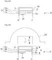
- FIG. 1is a view illustrating a conventional light emitting device module.
- a light emitting device 10is disposed on the bottom of a cavity of a package body 110 and a molding part 160 including phosphors 162 is charged around the light emitting device 10.
- the molding part 160may serve as a lens.
- a first lead frame 121 and a second lead frame 122may be arranged in the package body 110.
- the light emitting device 10may be electrically connected to the first lead frame 121 and the second lead frame 122 via wires 140 and 145 respectively.
- a reflective layer Rmay be formed on the surface of the package body 110 and serve to reflect light emitted from the light emitting device 10 upward.
- the package body 110may be connected to a circuit board 180 such as, for example, a Printed Circuit Board (PCB) to receive current required for driving of the light emitting device 10.
- a circuit board 180such as, for example, a Printed Circuit Board (PCB) to receive current required for driving of the light emitting device 10.
- PCBPrinted Circuit Board
- the conventional light emitting device module as described abovehas the following problems.
- the wires and the lead framesare required to supply current to the light emitting device and these materials may cause a cost increase. Moreover, the wires may hinder the progress of light emitted from the light emitting device, deteriorating light extraction efficiency.
- the reflective layer R as described abovemay be formed of a high reflectivity metal, thus being discolored.
- PPApolypthalamide
- US 2011/198643 A1discloses a light emitting device package including a body; first and second electrode layers on the body; a light emitting device electrically connected to the first and second electrode layers on the body; a luminescent layer on the light emitting device; and an encapsulant layer including particles on the luminescent layer.
- JP 2013 012516 Adiscloses a light-emitting device comprising a light-emitting element, a wavelength conversion layer which absorbs light from the light-emitting element to convert the light into light having a different wavelength; a protruding portion surrounding part or all of an upper surface of the wavelength conversion layer; and a wavelength conversion portion which absorbs light from the light-emitting element to convert the light into light having a different wavelength.
- US 2005/032257 A1discloses a method for bonding a transparent optical element to a light emitting device having stack of layers including semiconductor layers comprising an active region.
- the transparent optical elementcan be lens or optical concentrator.
- US 2014/103378 A1discloses a light emitting diode structure which has an optical lens placed on a substrate and an encapsulating ring-shaped dam, the light emitting diode being covered by a wavelength conversion material layer.
- Embodimentsprovide a light emitting device module which is capable of achieving reduced manufacturing costs and improved light extraction efficiency and preventing discoloration of, for example, a package body.
- a light emitting device moduleincludes the features as recited in claim 1.
- the phosphor layermay be disposed to extend from the side surface of the light emitting device to a surface of the circuit board, and the void may be generated in a region surrounded by the phosphor layer and the circuit board.
- the voidmay be filled with air.
- the light emitting devicemay be a flip chip type light emitting device.
- the phosphor layer disposed on the side surface of the light emitting devicemay be located higher than a height of the light emitting structure.
- the light emitting devicemay have a first side surface and a second side surface facing each other, and a distance between the phosphor layer and the circuit board at the first side surface may be equal to a distance between the phosphor layer and the circuit board at the second side surface.
- the phosphor layer and the lensmay comprise silicon.
- the lensmay come into contact with the phosphor layer and the circuit board.
- the lensmay have a recess and the light emitting device may be inserted into the recess.
- the recessmay have a depth equal to a height of the phosphor layer.
- a height of the phosphor layer at the side surface of the light emitting deviceis equal to a height of the light emitting device.
- a thickness of the phosphor layer at the side surface of the light emitting devicemay be equal to a thickness of the phosphor layer at the upper surface of the light emitting device.
- the light emitting devicemay have a first side surface and a second side surface facing each other, and a thickness of the phosphor layer at the first side surface may be equal to a thickness of the phosphor layer at the second side surface.
- a thickness of the lens at the periphery thereof outside the light emitting deviceis greater than a height of the light emitting device and less than the sum of the height of the light emitting device and a height of the phosphor layer.
- a thickness of the lens at the center thereofmay be within a range from two times to three times the sum of a height of the light emitting device and a height of the phosphor layer.
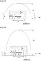
- FIG. 2is a view illustrating a first embodiment of a light emitting device module.
- the light emitting device moduleincludes a circuit board 280, a light emitting device 20 electrically connected to first and second conductive layers 281 and 282 on the circuit board 280, a phosphor layer 260 surrounding the light emitting device 20, and a lens 270 disposed over the phosphor layer 260 and the circuit board 280.
- the circuit board 280may be, for example, a Printed Circuit Board (PCB), a metal PCB, or an FR-4 board.
- the first conductive layer 281 and the second conductive layer 282 on the circuit board 280may be electrically connected to a first electrode 26a and a second electrode 26c of the light emitting device 20 respectively.
- the light emitting device 20may be a flip chip type light emitting device as illustrated.
- a buffer layer 22 and a light emitting structure 24are sequentially disposed on a substrate 21.
- the light emitting structure 24includes a first conductivity type (conductive) semiconductor layer 24a, an active layer 24b, and a second conductivity type (conductive) semiconductor layer 24c.
- the first electrode 26a and the second electrode 26cmay be disposed respectively on the first conductive semiconductor layer 24a and the second conductive semiconductor layer 24c.
- the substrate 21may be formed of a material suitable for semiconductor material growth, or a carrier wafer.
- the substrate 21may be formed of a highly thermally conductive material and include a conductive substrate or an insulation substrate.
- the substrate 21may utilize at least one selected from among sapphire (Al 2 O 3 ), SiO 2 , SiC, Si, GaAs, GaN, ZnO, GaP, InP, Ge, and Ga 2 O 3 .
- the buffer layer 22may be formed of AIN, for example.
- the first conductive semiconductor layer 24amay be formed of a compound semiconductor such as, for example, a group III-V or II-VI compound semiconductor and may be doped with a first conductive dopant.
- the first conductive semiconductor layer 24amay be formed of a semiconductor material having a composition of Al x In y Ga (1-x-y) N (0 ⁇ x ⁇ 1, 0 ⁇ y ⁇ 1, 0 ⁇ x+y ⁇ 1).
- the first conductive semiconductor layer 24amay be formed of any one or more materials selected from among AIGaN, GaN, InAIGaN, AIGaAs, GaP, GaAs, GaAsP, and AlGaInP.
- the first conductive dopantmay include an n-type dopant such as Si, Ge, Sn, Se, and Te.
- the first conductive semiconductor layer 24amay have a single layer or multi-layer form, without being limited thereto.
- the active layer 24bis disposed on the upper surface of the first conductive semiconductor layer 24a and may include any one of a single-well structure, a multi-well structure, a single-quantum well structure, a multi-quantum well structure, a quantum dot structure and a quantum wire structure.
- the active layer 24bis formed of a group III-V compound semiconductor and includes a well layer and a barrier layer having a pair structure of any one or more of AlGaN/AlGaN, InGaN/GaN, InGaN/InGaN, AIGaN/GaN, InAIGaN/GaN, GaAs(InGaAs)/AlGaAs, and GaP(InGaP)/AlGaP, without being limited thereto.
- the well layermay be formed of a material having a smaller energy band gap than an energy band gap of the barrier layer.
- the second conductive semiconductor layer 24cmay be formed of a compound semiconductor on the surface of the active layer 24b.
- the second conductive semiconductor layer 24cmay be formed of a compound semiconductor such as a group III-V or II-VI compound semiconductor and may be doped with a second conductive dopant.
- the second conductive semiconductor layer 24cmay be formed of, for example, a semiconductor material having a composition of In x Al y Ga 1-x-y N (0 ⁇ x ⁇ 1, 0 ⁇ y ⁇ 1, 0 ⁇ x+y ⁇ 1).
- the second conductive semiconductor layer 24cmay be formed of any one or more material selected from among AIGaN, GaN, AlInN, AlGaAs, GaP, GaAs, GaAsP, and AlGaInP.
- the second conductive semiconductor layer 24cmay be doped with the second conductive dopant.
- the second conductive dopantmay be a p-type dopant such as Mg, Zn, Ca, Sr, and Ba.
- the second conductive semiconductor layer 24cmay have a single layer or multi-layer form, without being limited thereto.
- a light transmission conductive layer formed of, for example, an Indium Tin Oxide (ITO)may be formed on the second conductive semiconductor layer 24c, which may improve current spreading effects from the second electrode 26c to the second conductive semiconductor layer 24c.
- ITOIndium Tin Oxide
- Portions of the second conductive semiconductor layer 24c, the active layer 24b and the first conductive semiconductor layer 24aare removed via mesa etching to expose the first conductive semiconductor layer 24a for acquisition of an area where the first electrode 26a will be formed.
- the first electrode 26a and the second electrode 26care disposed respectively on the first conductive semiconductor layer 24a and the second conductive semiconductor layer 24c.
- the first electrode 26a and the second electrode 26cmay be formed of at least one selected from among aluminum (Al), titanium (Ti), chrome (Cr), nickel (Ni), copper (Cu), and gold (Au) and have a single-layer or multi-layer form.
- a passivation layermay be formed around the light emitting structure 24.
- the passivation layermay be formed of an insulation material.
- the passivation layermay be formed of an oxide or nitride. More specifically, the passivation layer may be formed of a silicon oxide (SiO 2 ) layer, an oxide nitride layer, or an oxide aluminum layer.
- the first electrode 26a and the second electrode 26c of the light emitting device 20may be electrically connected to the first conductive layer 281 and the second conductive layer 282 of the circuit board 280 respectively via a conductive adhesive.
- solders 28a and 28cmay be used for bonding.
- the phosphor layer 260is disposed around the light emitting device 20.
- the phosphor layer 260is disposed on the upper surface and the side surface of the light emitting device 20.
- the phosphor layer 260extends from the side surface of the light emitting device 20 to the surface of the circuit board 280 so as to come into contact with the surface of the circuit board 280.
- the phosphor layer 260may comprise phosphors and a basic material comprising a silicon based polymer material such as, for example, a resin or rubber. As first wavelength light emitted from the light emitting device 20 excites the phosphors, second wavelength light may be emitted from the phosphors.
- Voidsmay be generated between the light emitting device 20 and the circuit board 280 in a region inside the phosphor layer 260.
- the voidsmay be filled with air.
- the phosphor layer 260surrounds the light emitting device 20 while coming into contact with the circuit board 280. Therefore, the voids may be generated in a region surrounded by the phosphor layer 260 on the side surface of the light emitting device 20 and the underlying circuit board 280. At this time, the voids may come into contact with the light emitting structure 24 of the light emitting device 20.
- the phosphor layer 260comes into contact with the light emitting device 20, more particularly, the upper surface of the substrate 21 at an area designated by "b1".
- the lens 270comes into contact with the phosphor layer 260 at an area designated by "b21” and also comes into contact with the circuit board 280 at an area designated by "b22”.
- the lens 270may comprise the same material as the above-described phosphor layer 260.
- the lens 270may comprise a silicon based polymer material such as, for example, a resin or rubber.
- the lens 270may have a convex portion at a central region thereof corresponding to the light emitting device 20.
- FIGs. 3A to 3Care views illustrating a process of manufacturing the light emitting device module of FIG. 2 .
- the phosphor layer 260is disposed around the flip chip type light emitting device 20.
- the phosphor layer 260may be disposed in a conformal coating or film form.
- the upper surfaces u2 and u1 of the phosphor layer 260may be respectively located higher than the first and second conductive semiconductor layers 24a and 24c or the first and second electrodes 26a and 26c.
- the phosphor layer 260 disposed around the light emitting device 20is inserted into a recess formed in the lens 270.
- a depth t of the recess formed in the lens 270is equal to a height h of the phosphor layer 260.
- the lens 270 and the phosphor layer 260may be attached to each other using the silicon based polymer material serving as a basic material as described above without requiring an adhesive.
- the light emitting device 20 inserted in the recess of the lens 270is coupled to the circuit board 280.
- solders 28a and 28cwhich serve as a conductive adhesive, are arranged on the first conductive layer 281 and the second conductive layer 282 on the circuit board 280.
- the first electrode 26a and the second electrode 26c of the light emitting device 20may be respectively fixed to the first conductive layer 281 and the second conductive layer 282 via the solders 28a and 28c.
- FIG. 4is a view illustrating a second embodiment of a light emitting device module.
- the light emitting device module 200b of the present embodimentis substantially equal to that of the above-described first embodiment, there is a difference in that the phosphor layer 260 does not come into contact with the circuit board 280.
- each of the upper surfaces u1 and u2 of the phosphor layer 260has the same height as the first conductive semiconductor layer 24a or the second conductive semiconductor layer 24c adjacent thereto, such that voids may laterally come into contact with the lens 270.
- FIG. 5is a view illustrating a third embodiment of a light emitting device module.
- the light emitting device module 200cis substantially equal to those of the first embodiment and the second embodiment as described above except that, while the heights of the upper surfaces u1 and u2 of the phosphor layer 260 are higher than those of the first conductive semiconductor layer 24a and the second conductive semiconductor layer 24c, the phosphor layer 260 may do not come into contact with the circuit board 280 and voids may laterally come into contact with the phosphor layer 260 and the lens 270.
- distances d1 and d2 between the upper surfaces u1 and u2 of the phosphor layer 260 and the circuit board 280may be equal to each other at both sides of the light emitting device 20.
- thicknesses t1 and t2 of the phosphor layer 260 at both sides of the light emitting device 20may be equal to a thickness t3 of the phosphor layer 260 at the upper surface of the light emitting device 20.
- wires and lead framesare omitted and the flip chip type light emitting device is directly coupled to the circuit board, which may result in reduced material costs and enhanced luminous efficacy owing to reduction in light absorption or shielding caused by wires.
- omission of a package body and a reflective layer on the package bodymay prevent distortion of color temperatures due to discoloration of the package body and the reflective layer.
- FIGs. 6A to 6Dare comparative views of light emitting device modules according to embodiments and a comparative embodiment.
- a light emitting deviceis briefly illustrated in a hexahedral shape and a circuit board below the light emitting device is omitted.
- a phosphor layeris disposed on the side surface and the upper surface of a light emitting device.
- Either side of the light emitting devicemay have a width w1 of 1000 ⁇ m and a height h1 of 250 ⁇ m.
- a thickness w2 of the phosphor layer at one side surface of the light emitting devicemay be 100 ⁇ m and a thickness h2 of the phosphor layer at the upper surface of the light emitting device may be 100 ⁇ m.
- a light emitting device and a phosphor layerhave the same shape as those of the comparative embodiment of FIG. 6A and there is a difference in that a lens is disposed on the side surface and the upper surface of the phosphor layer.
- the lensmay have a thickness h3 of 200 ⁇ m at the periphery thereof and may have a thickness h4 of 850 ⁇ m at the center thereof.
- the lenshas a central convex portion and the thickness h4 at the center of the lens may be a thickness of the convex portion.
- FIG. 6Cwhich is an embodiment of the invention as claimed, is identical to that of FIG. 6B except that the lens has a thickness h3 of 300 ⁇ m at the periphery thereof.
- FIG. 6Dis identical to that of FIG. 6B except that the lens has a thickness h4 of 1460 ⁇ m at the center thereof.
- the light output of the light emitting device module according to the comparative embodiment of FIG. 6Ais 100
- the light outputs of the light emitting device modules illustrated in FIGs. 6B to 6Dare respectively 106.7, 107.2 and 104.0.
- the view angle of the light emitting device module according to the comparative embodiment of FIG. 6Ais 137.3°
- the view angles of the light emitting device modules illustrated in FIGs. 6B to 6Dare respectively 150.29°, 143.88°, and 139.64°.
- the light output of the light emitting device moduleis improved.
- the light emitting device modules of FIGs. 6B and 6Cin which the thickness h4 of the lens at the center thereof is within a range from two times to three times the total height h1+h2 of the light emitting device and the phosphor layer, have higher light outputs and wider view angles than the light emitting device module of FIG. 6D in which the thickness h4 of the lens at the center thereof is four times or more the total height h1+h2 of the light emitting device and the phosphor layer.
- FIGs. 7A to 7Dare other comparative views of light emitting device modules according to embodiments and a comparative embodiment.
- a lensmay have a flat central region other than a convex central region.
- the light emitting device module of FIG. 7Afurther includes a lens disposed on the side surface and the upper surface of the phosphor layer as compared to the light emitting device module of FIG. 6A .
- Either side of the light emitting devicemay have the width w1 of 1000 ⁇ m and the height h1 of 250 ⁇ m.
- the thickness w2 of the phosphor layer at one side surface of the light emitting devicemay be 100 ⁇ m and the thickness h2 of the phosphor layer at the upper surface of the light emitting device may be 100 ⁇ m.
- a thickness w3 of the side surface of the lensmay be 100 ⁇ m and a thickness h3 of the upper surface of the lens may be 100 ⁇ m.
- the thickness h3 of the upper surface of the lensmay be 200 ⁇ m.
- the thickness w3 of the side surface of the lensmay be 200 ⁇ m.
- the thickness w3 of the side surface of the lens and the thickness h3 of the upper surface of the lensmay be 200 ⁇ m respectively.
- the light output of the light emitting device module according to the comparative embodiment of FIG. 6Ais 100
- the light outputs of the light emitting device modules illustrated in FIGs. 7A to 7Dare respectively 102.3, 102.8, 102.2 and 102.7.
- the view angle of the light emitting device module according to the comparative embodiment of FIG. 6Ais 137.3° and the view angles of the light emitting device modules illustrated in FIGs. 7A to 7D are respectively 143.15°, 145.78°, 142.21°, and 148.85°.
- the light emitting device module of FIG. 7Bwhen the thickness w3 of the side surface of the lens is equal to the thickness w2 of the side surface of the phosphor layer and the thickness h3 of the upper surface of the lens is about two times the thickness h2 of the upper surface of the phosphor layer, the light emitting device module may has the greatest light output.
- the light emitting device module of FIG. 7Bwhen the thickness w3 of the side surface of the lens is equal to the thickness w2 of the side surface of the phosphor layer and the thickness h3 of the upper surface of the lens is about two times the thickness h2 of the upper surface of the phosphor layer, the light emitting device module may has the greatest light output.
- the light emitting device modulemay have the greatest view angle.
- the light emitting device module as described abovemay be used as a light source.
- the light emitting device modulemay be used as a light source of, for example, an image display apparatus and a lighting apparatus.
- FIGs. 8A to 8Care views illustrating an array of the light emitting device modules as described above.
- the light emitting device modules 200a as described abovemay be arranged in a single line on a single circuit board 280 so as to be used in a lighting apparatus or to be used as an edge type light source in an image display apparatus.
- a plurality of light emitting device modulesmay be arranged in plural rows and columns on a single circuit board 280.
- the light emitting device modulesmay be used as a vertical type light source in an image display apparatus.
- the light emitting device modulesWhen the light emitting device modules are used as a light source of an image display apparatus or a lighting apparatus, reduced material costs and enhanced luminous efficacy may be accomplished and the entire light source may achieve uniform color temperature.
- a light emitting device modulemay achieve reduced material costs and enhanced luminous efficacy owing to reduction in light absorption or shielding caused by wires because wires and lead frames are omitted and a flip chip type light emitting device is directly coupled to a circuit board.
- the light emitting device modulemay prevent distortion of color temperatures due to discoloration of the package body and the reflective layer.
Landscapes
- Led Device Packages (AREA)
Description
- This application claims priority to Korean Patent Application No.
10-2014-0066694 - Embodiments relate to a light emitting device module.
- Group III-V compound semiconductors such as, for example, GaN and AIGaN are widely used for optoelectronics and electronics because of many advantages such as, for example, easily controllable wide band gap energy.
- In particular, light emitting devices, such as light emitting diodes or laser diodes, which use group III-V or II-VI compound semiconductors, are capable of emitting visible and ultraviolet light of various colors such as red, green, and blue owing to development of device materials and thin film growth techniques. These light emitting devices are also capable of emitting white light with high luminous efficacy through use of phosphors or color combination and have several advantages of low power consumption, semi-permanent lifespan, fast response speed, safety, and environmental friendliness as compared to conventional light sources such as, for example, fluorescent lamps and incandescent lamps.
- Accordingly, application sectors of the light emitting devices are expanded up to transmission modules of optical communication means, light emitting diode backlights to replace Cold Cathode Fluorescence Lamps (CCFLs) which serve as backlights of Liquid Crystal Display (LCD) apparatuses, white light emitting diode lighting apparatus to replace fluorescent lamps or incandescent lamps, vehicular headlamps, and traffic lights.
- In a light emitting device, a light emitting structure, which includes a first conductive semiconductor layer, an active layer, and a second conductive semiconductor layer, is disposed on a substrate formed of, for example, sapphire and a first electrode and a second electrode are respectively disposed on the first conductive semiconductor layer and the second conductive semiconductor layer. The light emitting device emits light having energy determined by an intrinsic energy-band of a material constituting the active layer in which electrons introduced through the first conductive semiconductor layer and holes introduced through the second conductive semiconductor layer meet each other. Light emitted from the active layer may vary based on the composition of the material constituting the active layer, and may be blue light, ultraviolet (UV) or deep UV light, for example.
- The light emitting device as described above may be mounted in a package form to, for example, a backlight unit or a lighting apparatus.
FIG. 1 is a view illustrating a conventional light emitting device module.- In the light
emitting device module 100, alight emitting device 10 is disposed on the bottom of a cavity of apackage body 110 and amolding part 160 includingphosphors 162 is charged around thelight emitting device 10. Themolding part 160 may serve as a lens. - A
first lead frame 121 and asecond lead frame 122 may be arranged in thepackage body 110. Thelight emitting device 10 may be electrically connected to thefirst lead frame 121 and thesecond lead frame 122 viawires - A reflective layer R may be formed on the surface of the
package body 110 and serve to reflect light emitted from thelight emitting device 10 upward. - The
package body 110 may be connected to acircuit board 180 such as, for example, a Printed Circuit Board (PCB) to receive current required for driving of thelight emitting device 10. - However, the conventional light emitting device module as described above has the following problems.
- The wires and the lead frames are required to supply current to the light emitting device and these materials may cause a cost increase. Moreover, the wires may hinder the progress of light emitted from the light emitting device, deteriorating light extraction efficiency.
- In addition, the reflective layer R as described above may be formed of a high reflectivity metal, thus being discolored. For example, polypthalamide (PPA) constituting the package body may be easily discolored by heat.
US 2011/198643 A1 discloses a light emitting device package including a body; first and second electrode layers on the body; a light emitting device electrically connected to the first and second electrode layers on the body; a luminescent layer on the light emitting device; and an encapsulant layer including particles on the luminescent layer.JP 2013 012516 A US 2005/032257 A1 discloses a method for bonding a transparent optical element to a light emitting device having stack of layers including semiconductor layers comprising an active region. The transparent optical element can be lens or optical concentrator.US 2014/103378 A1 discloses a light emitting diode structure which has an optical lens placed on a substrate and an encapsulating ring-shaped dam, the light emitting diode being covered by a wavelength conversion material layer.- Embodiments provide a light emitting device module which is capable of achieving reduced manufacturing costs and improved light extraction efficiency and preventing discoloration of, for example, a package body.
- In one embodiment, a light emitting device module includes the features as recited in claim 1.
- The phosphor layer may be disposed to extend from the side surface of the light emitting device to a surface of the circuit board, and the void may be generated in a region surrounded by the phosphor layer and the circuit board.
- The void may be filled with air.
- The light emitting device may be a flip chip type light emitting device.
- The phosphor layer disposed on the side surface of the light emitting device may be located higher than a height of the light emitting structure.
- The light emitting device may have a first side surface and a second side surface facing each other, and a distance between the phosphor layer and the circuit board at the first side surface may be equal to a distance between the phosphor layer and the circuit board at the second side surface.
- The phosphor layer and the lens may comprise silicon.
- The lens may come into contact with the phosphor layer and the circuit board.
- The lens may have a recess and the light emitting device may be inserted into the recess.
- The recess may have a depth equal to a height of the phosphor layer.
- A height of the phosphor layer at the side surface of the light emitting device is equal to a height of the light emitting device.
- A thickness of the phosphor layer at the side surface of the light emitting device may be equal to a thickness of the phosphor layer at the upper surface of the light emitting device.
- The light emitting device may have a first side surface and a second side surface facing each other, and a thickness of the phosphor layer at the first side surface may be equal to a thickness of the phosphor layer at the second side surface.
- A thickness of the lens at the periphery thereof outside the light emitting device is greater than a height of the light emitting device and less than the sum of the height of the light emitting device and a height of the phosphor layer.
- A thickness of the lens at the center thereof may be within a range from two times to three times the sum of a height of the light emitting device and a height of the phosphor layer.
- This disclosure comprises embodiments, some of which are embodiments of the invention as claimed.
- Arrangements and embodiments may be described in detail with reference to the following drawings in which like reference numerals refer to like elements and wherein:
FIG. 1 is a view illustrating a conventional light emitting device module;FIG. 2 is a view illustrating a first embodiment of a light emitting device module;FIGs. 3A to 3C are views illustrating a process of manufacturing the light emitting device module ofFIG. 2 ;FIG. 4 is a view illustrating a second embodiment of a light emitting device module;FIG. 5 is a view illustrating a third embodiment of a light emitting device module;FIGs. 6A to 6D are comparative views of light emitting device modules according to embodiments and a comparative embodiment;FIG. 6C is an embodiment of the invention as claimed;FIGs. 7A to 7D are other comparative views of light emitting device modules according to embodiments and a comparative embodiment;FIGs. 8A to 8C are views illustrating an array of the above-described light emitting device modules.- Hereinafter, exemplary embodiments to concretely realize the above objects will be described in detail with reference to the accompanying drawings.
- In the following description of the embodiments, it will be understood that, when each element is referred to as being formed "on" or "under" the other element, it can be directly "on" or "under" the other element or be indirectly formed with one or more intervening elements therebetween. In addition, it will also be understood that "on" or "under" the element may mean an upward direction and a downward direction of the element.
FIG. 2 is a view illustrating a first embodiment of a light emitting device module.- The light emitting device module according to the present embodiment, designated by
reference numeral 200a, includes acircuit board 280, alight emitting device 20 electrically connected to first and secondconductive layers circuit board 280, aphosphor layer 260 surrounding thelight emitting device 20, and alens 270 disposed over thephosphor layer 260 and thecircuit board 280. - The
circuit board 280 may be, for example, a Printed Circuit Board (PCB), a metal PCB, or an FR-4 board. The firstconductive layer 281 and the secondconductive layer 282 on thecircuit board 280 may be electrically connected to afirst electrode 26a and asecond electrode 26c of thelight emitting device 20 respectively. - The
light emitting device 20 may be a flip chip type light emitting device as illustrated. Abuffer layer 22 and alight emitting structure 24 are sequentially disposed on asubstrate 21. Thelight emitting structure 24 includes a first conductivity type (conductive)semiconductor layer 24a, anactive layer 24b, and a second conductivity type (conductive)semiconductor layer 24c. Thefirst electrode 26a and thesecond electrode 26c may be disposed respectively on the firstconductive semiconductor layer 24a and the secondconductive semiconductor layer 24c. - The
substrate 21 may be formed of a material suitable for semiconductor material growth, or a carrier wafer. Thesubstrate 21 may be formed of a highly thermally conductive material and include a conductive substrate or an insulation substrate. For example, thesubstrate 21 may utilize at least one selected from among sapphire (Al2O3), SiO2, SiC, Si, GaAs, GaN, ZnO, GaP, InP, Ge, and Ga2O3. - When the
substrate 21 is formed of, for example, sapphire and thelight emitting structure 24 comprising, for example, GaN or AIGaN is disposed on thesubstrate 21, for example, dislocation, melt-back, cracking, pitting, and surface morphology defects that deteriorate crystallization may occur due to great lattice mismatch between GaN or AIGaN and sapphire and a great difference between thermal expansion coefficients thereof. Therefore, thebuffer layer 22 may be formed of AIN, for example. - The first
conductive semiconductor layer 24a may be formed of a compound semiconductor such as, for example, a group III-V or II-VI compound semiconductor and may be doped with a first conductive dopant. The firstconductive semiconductor layer 24a may be formed of a semiconductor material having a composition of AlxInyGa(1-x-y)N (0≤x≤1, 0≤y≤1, 0≤x+y≤1). For example, the firstconductive semiconductor layer 24a may be formed of any one or more materials selected from among AIGaN, GaN, InAIGaN, AIGaAs, GaP, GaAs, GaAsP, and AlGaInP. - When the first
conductive semiconductor layer 24a is an n-type semiconductor layer, the first conductive dopant may include an n-type dopant such as Si, Ge, Sn, Se, and Te. The firstconductive semiconductor layer 24a may have a single layer or multi-layer form, without being limited thereto. - The
active layer 24b is disposed on the upper surface of the firstconductive semiconductor layer 24a and may include any one of a single-well structure, a multi-well structure, a single-quantum well structure, a multi-quantum well structure, a quantum dot structure and a quantum wire structure. - The
active layer 24b is formed of a group III-V compound semiconductor and includes a well layer and a barrier layer having a pair structure of any one or more of AlGaN/AlGaN, InGaN/GaN, InGaN/InGaN, AIGaN/GaN, InAIGaN/GaN, GaAs(InGaAs)/AlGaAs, and GaP(InGaP)/AlGaP, without being limited thereto. The well layer may be formed of a material having a smaller energy band gap than an energy band gap of the barrier layer. - The second
conductive semiconductor layer 24c may be formed of a compound semiconductor on the surface of theactive layer 24b. The secondconductive semiconductor layer 24c may be formed of a compound semiconductor such as a group III-V or II-VI compound semiconductor and may be doped with a second conductive dopant. The secondconductive semiconductor layer 24c may be formed of, for example, a semiconductor material having a composition of InxAlyGa1-x-yN (0≤x≤1, 0≤y≤1, 0≤x+y≤1). For example, the secondconductive semiconductor layer 24c may be formed of any one or more material selected from among AIGaN, GaN, AlInN, AlGaAs, GaP, GaAs, GaAsP, and AlGaInP. - The second
conductive semiconductor layer 24c may be doped with the second conductive dopant. When the secondconductive semiconductor layer 24c is a p-type semiconductor layer, the second conductive dopant may be a p-type dopant such as Mg, Zn, Ca, Sr, and Ba. The secondconductive semiconductor layer 24c may have a single layer or multi-layer form, without being limited thereto. - Although not illustrated, a light transmission conductive layer formed of, for example, an Indium Tin Oxide (ITO) may be formed on the second
conductive semiconductor layer 24c, which may improve current spreading effects from thesecond electrode 26c to the secondconductive semiconductor layer 24c. - Portions of the second
conductive semiconductor layer 24c, theactive layer 24b and the firstconductive semiconductor layer 24a are removed via mesa etching to expose the firstconductive semiconductor layer 24a for acquisition of an area where thefirst electrode 26a will be formed. - The
first electrode 26a and thesecond electrode 26c are disposed respectively on the firstconductive semiconductor layer 24a and the secondconductive semiconductor layer 24c. Thefirst electrode 26a and thesecond electrode 26c may be formed of at least one selected from among aluminum (Al), titanium (Ti), chrome (Cr), nickel (Ni), copper (Cu), and gold (Au) and have a single-layer or multi-layer form. - Although not illustrated, a passivation layer may be formed around the
light emitting structure 24. The passivation layer may be formed of an insulation material. Specifically, the passivation layer may be formed of an oxide or nitride. More specifically, the passivation layer may be formed of a silicon oxide (SiO2) layer, an oxide nitride layer, or an oxide aluminum layer. - The
first electrode 26a and thesecond electrode 26c of thelight emitting device 20 may be electrically connected to the firstconductive layer 281 and the secondconductive layer 282 of thecircuit board 280 respectively via a conductive adhesive. In the present embodiment, solders 28a and 28c may be used for bonding. - The
phosphor layer 260 is disposed around thelight emitting device 20. Thephosphor layer 260 is disposed on the upper surface and the side surface of thelight emitting device 20. - In the present embodiment, the
phosphor layer 260 extends from the side surface of thelight emitting device 20 to the surface of thecircuit board 280 so as to come into contact with the surface of thecircuit board 280. - The
phosphor layer 260 may comprise phosphors and a basic material comprising a silicon based polymer material such as, for example, a resin or rubber. As first wavelength light emitted from thelight emitting device 20 excites the phosphors, second wavelength light may be emitted from the phosphors. - Voids may be generated between the light emitting
device 20 and thecircuit board 280 in a region inside thephosphor layer 260. The voids may be filled with air. - In the present embodiment, the
phosphor layer 260 surrounds thelight emitting device 20 while coming into contact with thecircuit board 280. Therefore, the voids may be generated in a region surrounded by thephosphor layer 260 on the side surface of thelight emitting device 20 and theunderlying circuit board 280. At this time, the voids may come into contact with thelight emitting structure 24 of thelight emitting device 20. - In
FIG. 2 , thephosphor layer 260 comes into contact with thelight emitting device 20, more particularly, the upper surface of thesubstrate 21 at an area designated by "b1". Thelens 270 comes into contact with thephosphor layer 260 at an area designated by "b21" and also comes into contact with thecircuit board 280 at an area designated by "b22". - The
lens 270 may comprise the same material as the above-describedphosphor layer 260. Specifically, thelens 270 may comprise a silicon based polymer material such as, for example, a resin or rubber. As exemplarily illustrated, thelens 270 may have a convex portion at a central region thereof corresponding to thelight emitting device 20. FIGs. 3A to 3C are views illustrating a process of manufacturing the light emitting device module ofFIG. 2 .- As exemplarily illustrated in
FIG. 3A , thephosphor layer 260 is disposed around the flip chip typelight emitting device 20. Thephosphor layer 260 may be disposed in a conformal coating or film form. As illustrated, the upper surfaces u2 and u1 of thephosphor layer 260 may be respectively located higher than the first and secondconductive semiconductor layers second electrodes - Then, as exemplarily illustrated in
FIG. 3B , thephosphor layer 260 disposed around thelight emitting device 20 is inserted into a recess formed in thelens 270. At this time, a depth t of the recess formed in thelens 270 is equal to a height h of thephosphor layer 260. At this time, thelens 270 and thephosphor layer 260 may be attached to each other using the silicon based polymer material serving as a basic material as described above without requiring an adhesive. - Then, as exemplarily illustrated in
FIG. 3C , thelight emitting device 20 inserted in the recess of thelens 270 is coupled to thecircuit board 280. - At this time, the
solders conductive layer 281 and the secondconductive layer 282 on thecircuit board 280. Thefirst electrode 26a and thesecond electrode 26c of thelight emitting device 20 may be respectively fixed to the firstconductive layer 281 and the secondconductive layer 282 via thesolders FIG. 4 is a view illustrating a second embodiment of a light emitting device module.- Although the light emitting device module 200b of the present embodiment is substantially equal to that of the above-described first embodiment, there is a difference in that the
phosphor layer 260 does not come into contact with thecircuit board 280. - That is, each of the upper surfaces u1 and u2 of the
phosphor layer 260 has the same height as the firstconductive semiconductor layer 24a or the secondconductive semiconductor layer 24c adjacent thereto, such that voids may laterally come into contact with thelens 270. FIG. 5 is a view illustrating a third embodiment of a light emitting device module.- The light emitting
device module 200c according to the present embodiment is substantially equal to those of the first embodiment and the second embodiment as described above except that, while the heights of the upper surfaces u1 and u2 of thephosphor layer 260 are higher than those of the firstconductive semiconductor layer 24a and the secondconductive semiconductor layer 24c, thephosphor layer 260 may do not come into contact with thecircuit board 280 and voids may laterally come into contact with thephosphor layer 260 and thelens 270. - In
FIG. 5 , distances d1 and d2 between the upper surfaces u1 and u2 of thephosphor layer 260 and thecircuit board 280 may be equal to each other at both sides of thelight emitting device 20. In addition, thicknesses t1 and t2 of thephosphor layer 260 at both sides of thelight emitting device 20 may be equal to a thickness t3 of thephosphor layer 260 at the upper surface of thelight emitting device 20. - In the light emitting device modules according to the embodiments, wires and lead frames are omitted and the flip chip type light emitting device is directly coupled to the circuit board, which may result in reduced material costs and enhanced luminous efficacy owing to reduction in light absorption or shielding caused by wires. In addition, omission of a package body and a reflective layer on the package body may prevent distortion of color temperatures due to discoloration of the package body and the reflective layer.
FIGs. 6A to 6D are comparative views of light emitting device modules according to embodiments and a comparative embodiment. InFIGs. 6A to 6D , a light emitting device is briefly illustrated in a hexahedral shape and a circuit board below the light emitting device is omitted.- In the comparative embodiment of
FIG. 6A , a phosphor layer is disposed on the side surface and the upper surface of a light emitting device. Either side of the light emitting device may have a width w1 of 1000µm and a height h1 of 250µm. In addition, a thickness w2 of the phosphor layer at one side surface of the light emitting device may be 100µm and a thickness h2 of the phosphor layer at the upper surface of the light emitting device may be 100µm. - In the embodiment of
FIG. 6B , a light emitting device and a phosphor layer have the same shape as those of the comparative embodiment ofFIG. 6A and there is a difference in that a lens is disposed on the side surface and the upper surface of the phosphor layer. The lens may have a thickness h3 of 200µm at the periphery thereof and may have a thickness h4 of 850µm at the center thereof. Here, the lens has a central convex portion and the thickness h4 at the center of the lens may be a thickness of the convex portion. - The embodiment of
FIG. 6C , which is an embodiment of the invention as claimed, is identical to that ofFIG. 6B except that the lens has a thickness h3 of 300µm at the periphery thereof. - The embodiment of
FIG. 6D is identical to that ofFIG. 6B except that the lens has a thickness h4 of 1460µm at the center thereof. - Assuming that the light output of the light emitting device module according to the comparative embodiment of
FIG. 6A is 100, the light outputs of the light emitting device modules illustrated inFIGs. 6B to 6D are respectively 106.7, 107.2 and 104.0. In addition, the view angle of the light emitting device module according to the comparative embodiment ofFIG. 6A is 137.3°, and the view angles of the light emitting device modules illustrated inFIGs. 6B to 6D are respectively 150.29°, 143.88°, and 139.64°. - In
FIGs. 6A to 6D , when the thickness h3 of the lens at the periphery thereof is greater than the height h1 of the light emitting device and less than the total height h1+h2 of the light emitting device and the phosphor layer, the light output of the light emitting device module is improved. In addition, the light emitting device modules ofFIGs. 6B and6C , in which the thickness h4 of the lens at the center thereof is within a range from two times to three times the total height h1+h2 of the light emitting device and the phosphor layer, have higher light outputs and wider view angles than the light emitting device module ofFIG. 6D in which the thickness h4 of the lens at the center thereof is four times or more the total height h1+h2 of the light emitting device and the phosphor layer. FIGs. 7A to 7D are other comparative views of light emitting device modules according to embodiments and a comparative embodiment.- Differently from the light emitting device modules of
FIGs. 6B to 6D , in the light emitting device modules ofFIGs. 7A to 7D , a lens may have a flat central region other than a convex central region. - The light emitting device module of
FIG. 7A further includes a lens disposed on the side surface and the upper surface of the phosphor layer as compared to the light emitting device module ofFIG. 6A . Either side of the light emitting device may have the width w1 of 1000µm and the height h1 of 250µm. The thickness w2 of the phosphor layer at one side surface of the light emitting device may be 100µm and the thickness h2 of the phosphor layer at the upper surface of the light emitting device may be 100µm. In addition, a thickness w3 of the side surface of the lens may be 100µm and a thickness h3 of the upper surface of the lens may be 100µm. - Although the light emitting device module of
FIG. 7B is identical to that of the embodiment ofFIG. 7A , the thickness h3 of the upper surface of the lens may be 200µm. - Although the light emitting device module of
FIG. 7C is identical to that of the embodiment ofFIG. 7A , the thickness w3 of the side surface of the lens may be 200µm. - Although the light emitting device module of
FIG. 7D is identical to that of the embodiment ofFIG. 7A , the thickness w3 of the side surface of the lens and the thickness h3 of the upper surface of the lens may be 200µm respectively. - Assuming that the light output of the light emitting device module according to the comparative embodiment of
FIG. 6A is 100, the light outputs of the light emitting device modules illustrated inFIGs. 7A to 7D are respectively 102.3, 102.8, 102.2 and 102.7. In addition, the view angle of the light emitting device module according to the comparative embodiment ofFIG. 6A is 137.3° and the view angles of the light emitting device modules illustrated inFIGs. 7A to 7D are respectively 143.15°, 145.78°, 142.21°, and 148.85°. - In
FIGs. 7A to 7D , when the lens is disposed on the upper surface and the side surface of the phosphor layer, the light output is improved and the view angle is increased. In particular, as in the light emitting device module ofFIG. 7B , when the thickness w3 of the side surface of the lens is equal to the thickness w2 of the side surface of the phosphor layer and the thickness h3 of the upper surface of the lens is about two times the thickness h2 of the upper surface of the phosphor layer, the light emitting device module may has the greatest light output. In addition, as in the light emitting device module ofFIG. 7D , when the thickness w3 of the side surface of the lens and the thickness h3 of the upper surface of the lens are respectively about two times the thickness w2 of the side surface of the phosphor layer and the thickness h2 of the upper surface of the phosphor layer, the light emitting device module may have the greatest view angle. - The light emitting device module as described above may be used as a light source. For example, the light emitting device module may be used as a light source of, for example, an image display apparatus and a lighting apparatus.
FIGs. 8A to 8C are views illustrating an array of the light emitting device modules as described above.- As exemplarily illustrated in
FIGs. 8A and8B , the light emittingdevice modules 200a as described above may be arranged in a single line on asingle circuit board 280 so as to be used in a lighting apparatus or to be used as an edge type light source in an image display apparatus. - As exemplarily illustrated in
FIG. 8C , a plurality of light emitting device modules may be arranged in plural rows and columns on asingle circuit board 280. In particular, the light emitting device modules may be used as a vertical type light source in an image display apparatus. - When the light emitting device modules are used as a light source of an image display apparatus or a lighting apparatus, reduced material costs and enhanced luminous efficacy may be accomplished and the entire light source may achieve uniform color temperature.
- As is apparent from the above description, a light emitting device module according to the embodiments may achieve reduced material costs and enhanced luminous efficacy owing to reduction in light absorption or shielding caused by wires because wires and lead frames are omitted and a flip chip type light emitting device is directly coupled to a circuit board. In addition, through omission of a package body and a reflective layer on the package body, the light emitting device module may prevent distortion of color temperatures due to discoloration of the package body and the reflective layer.
- Although embodiments have been described with reference to a number of illustrative embodiments thereof, it should be understood that numerous other modifications and embodiments can be devised by those skilled in the art. More particularly, various variations and modifications are possible in the component parts and/or arrangements of the subject combination arrangement within the scope of the appended claims, which define the invention. In addition to variations and modifications in the component parts and/or arrangements, alternative uses will also be apparent to those skilled in the art.
Claims (10)
- A light emitting device module comprising:a circuit board (280);a light emitting device (20) bonded to a conductive layer (281, 282) on the circuit board (280) via a conductive adhesive (28a, 28c),the light emitting device (20) comprising a light emitting structure (24) on a substrate (21) and the light emitting structure (24) comprising a first conductivity type semiconductor layer (24a), an active layer (24b) and a second conductivity type semiconductor layer (24c);a phosphor layer (260) disposed on a side surface and an upper surface of the light emitting device (20); anda lens (270) disposed on the circuit board (270) and the phosphor layer (260),wherein a void is disposed between the light emitting structure (24) and the circuit board (280); anda height of the phosphor layer (260) at the side surface of the light emitting device (20) is equal to a height of the light emitting device (20);characterized in thatthe thickness of the lens (270) at the periphery thereof outside of the light emitting device (20) is greater than a height of the light emitting device (20) and less than the sum of the height of the light emitting device (20) and a height of the phosphor layer (260).
- The module according to claim 1, wherein the void is filled with air.
- The module according to claim 1, wherein the light emitting device (20) is a flip chip type light emitting device (20).
- The module according to claim 1, wherein the phosphor layer (260) disposed on the side surface of the light emitting device (20) is located higher than a height of the light emitting structure (24).
- The module according to claim 1, wherein the lens (270) comes into contact with the phosphor layer (260) and the circuit board(280).
- The module according to claim 1, wherein the lens (270) has a recess and the light emitting device (20) is disposed in the recess.
- The module according to claim 6, wherein the recess has a depth equal to a height of the phosphor layer (260).
- The module according to claim 1, wherein a thickness of the phosphor layer (260) at the side surface of the light emitting device (20) is equal to a thickness of the phosphor layer (260) at the upper surface of the light emitting device (20).
- The module according to claim 1, wherein the light emitting device (20) has a first side surface and a second side surface facing each other, and a thickness of the phosphor layer (260) at the first side surface is equal to a thickness of the phosphor layer (260) at the second side surface.
- The module according to claim 1, wherein a height of the lens (270) is within a range from two times to three times the sum of a height of the light emitting device (20) and a height of the phosphor layer(260).
Applications Claiming Priority (1)
| Application Number | Priority Date | Filing Date | Title |
|---|---|---|---|
| KR1020140066694AKR102189129B1 (en) | 2014-06-02 | 2014-06-02 | Light emitting device module |
Publications (2)
| Publication Number | Publication Date |
|---|---|
| EP2953175A1 EP2953175A1 (en) | 2015-12-09 |
| EP2953175B1true EP2953175B1 (en) | 2018-10-24 |
Family
ID=53269414
Family Applications (1)
| Application Number | Title | Priority Date | Filing Date |
|---|---|---|---|
| EP15170349.3ANot-in-forceEP2953175B1 (en) | 2014-06-02 | 2015-06-02 | Light emitting device module |
Country Status (4)
| Country | Link |
|---|---|
| US (1) | US9768363B2 (en) |
| EP (1) | EP2953175B1 (en) |
| KR (1) | KR102189129B1 (en) |
| CN (1) | CN105322084A (en) |
Families Citing this family (9)
| Publication number | Priority date | Publication date | Assignee | Title |
|---|---|---|---|---|
| DE102017102112A1 (en)* | 2016-02-04 | 2017-08-10 | Epistar Corporation | Light-emitting element and its production method |
| JP6955135B2 (en) | 2016-10-19 | 2021-10-27 | 日亜化学工業株式会社 | Light emitting device and its manufacturing method |
| US10325791B1 (en)* | 2017-12-13 | 2019-06-18 | Facebook Technologies, Llc | Formation of elastomeric layer on selective regions of light emitting device |
| KR102675945B1 (en)* | 2018-09-18 | 2024-06-17 | 삼성전자주식회사 | A light-generating device |
| CN111477732B (en) | 2019-01-24 | 2021-10-08 | 隆达电子股份有限公司 | Light emitting device |
| KR102787183B1 (en)* | 2019-10-02 | 2025-03-28 | 삼성디스플레이 주식회사 | Display device and fabricating method for display device |
| KR102294340B1 (en)* | 2019-10-10 | 2021-08-26 | 셀리온 주식회사 | Led illuminating apparatus with high radiation angle of light using three-dimensional printing process and method for manufacturing the same |
| KR102791690B1 (en)* | 2020-01-08 | 2025-04-07 | 엘지전자 주식회사 | Method of display device using semiconductor light emitting devices |
| WO2022119050A1 (en)* | 2020-12-03 | 2022-06-09 | 삼성전자주식회사 | Led chip and display device comprising same |
Citations (4)
| Publication number | Priority date | Publication date | Assignee | Title |
|---|---|---|---|---|
| US20050032257A1 (en)* | 2000-09-12 | 2005-02-10 | Camras Michael D. | Method of forming light emitting devices with improved light extraction efficiency |
| KR20090040770A (en)* | 2007-10-22 | 2009-04-27 | 삼성전기주식회사 | Light emitting diode chip, manufacturing method and high output light emitting device |
| DE102011080458A1 (en)* | 2011-08-04 | 2013-02-07 | Osram Opto Semiconductors Gmbh | OPTOELECTRONIC ARRANGEMENT AND METHOD FOR PRODUCING AN OPTOELECTRONIC ARRANGEMENT |
| JP2013138132A (en)* | 2011-12-28 | 2013-07-11 | Nichia Chem Ind Ltd | Manufacturing method of light emitting device |
Family Cites Families (15)
| Publication number | Priority date | Publication date | Assignee | Title |
|---|---|---|---|---|
| KR101311635B1 (en)* | 2003-12-09 | 2013-09-26 | 젤코어 엘엘씨 | Surface mount light emitting chip package |
| US7352011B2 (en) | 2004-11-15 | 2008-04-01 | Philips Lumileds Lighting Company, Llc | Wide emitting lens for LED useful for backlighting |
| JP5038631B2 (en)* | 2006-02-03 | 2012-10-03 | 新光電気工業株式会社 | Light emitting device |
| US9660153B2 (en)* | 2007-11-14 | 2017-05-23 | Cree, Inc. | Gap engineering for flip-chip mounted horizontal LEDs |
| US20100109025A1 (en)* | 2008-11-05 | 2010-05-06 | Koninklijke Philips Electronics N.V. | Over the mold phosphor lens for an led |
| US8044420B2 (en)* | 2009-01-15 | 2011-10-25 | Advanced Semiconductor Engineering, Inc. | Light emitting diode package structure |
| KR20110080318A (en)* | 2010-01-05 | 2011-07-13 | 엘지이노텍 주식회사 | Light emitting device package |
| KR20120032899A (en) | 2010-09-29 | 2012-04-06 | 삼성엘이디 주식회사 | Light emitting diode package and manufacturing method for the same |
| KR20120078878A (en) | 2011-01-03 | 2012-07-11 | 삼성엘이디 주식회사 | Light distribution lens and light module of illumination device having the same |
| KR20120119350A (en)* | 2011-04-21 | 2012-10-31 | 삼성전자주식회사 | Light emitting device module and method for manufacturing the same |
| JP5772293B2 (en) | 2011-06-28 | 2015-09-02 | 日亜化学工業株式会社 | Light emitting device and manufacturing method thereof |
| GB2506138B (en) | 2012-09-20 | 2014-11-19 | Cooper Technologies Co | Lens and light emitting device incorporating a lens |
| TWI481083B (en)* | 2012-10-16 | 2015-04-11 | Lextar Electronics Corp | Light-emitting diode structure |
| US9318674B2 (en)* | 2013-02-05 | 2016-04-19 | Cree, Inc. | Submount-free light emitting diode (LED) components and methods of fabricating same |
| CN203351658U (en) | 2013-07-29 | 2013-12-18 | 深圳市天电光电科技有限公司 | White-light LED lighting structure |
- 2014
- 2014-06-02KRKR1020140066694Apatent/KR102189129B1/ennot_activeExpired - Fee Related
- 2015
- 2015-06-01USUS14/726,944patent/US9768363B2/enactiveActive
- 2015-06-02CNCN201510295516.8Apatent/CN105322084A/enactivePending
- 2015-06-02EPEP15170349.3Apatent/EP2953175B1/ennot_activeNot-in-force
Patent Citations (4)
| Publication number | Priority date | Publication date | Assignee | Title |
|---|---|---|---|---|
| US20050032257A1 (en)* | 2000-09-12 | 2005-02-10 | Camras Michael D. | Method of forming light emitting devices with improved light extraction efficiency |
| KR20090040770A (en)* | 2007-10-22 | 2009-04-27 | 삼성전기주식회사 | Light emitting diode chip, manufacturing method and high output light emitting device |
| DE102011080458A1 (en)* | 2011-08-04 | 2013-02-07 | Osram Opto Semiconductors Gmbh | OPTOELECTRONIC ARRANGEMENT AND METHOD FOR PRODUCING AN OPTOELECTRONIC ARRANGEMENT |
| JP2013138132A (en)* | 2011-12-28 | 2013-07-11 | Nichia Chem Ind Ltd | Manufacturing method of light emitting device |
Also Published As
| Publication number | Publication date |
|---|---|
| KR20150138605A (en) | 2015-12-10 |
| EP2953175A1 (en) | 2015-12-09 |
| US20150349219A1 (en) | 2015-12-03 |
| KR102189129B1 (en) | 2020-12-09 |
| CN105322084A (en) | 2016-02-10 |
| US9768363B2 (en) | 2017-09-19 |
Similar Documents
| Publication | Publication Date | Title |
|---|---|---|
| EP2953175B1 (en) | Light emitting device module | |
| US9559278B2 (en) | Light emitting device package | |
| CN111164753B (en) | Semiconductor device and headlamp comprising same | |
| EP2830094B1 (en) | Light emitting device | |
| US10361351B2 (en) | Semiconductor light emitting element package including solder bump | |
| US8741671B2 (en) | Method for manufacturing light emitting device having an active layer formed over a Ga-face | |
| CN109757120B (en) | Light emitting device packaging | |
| KR20180040073A (en) | Light emitting device, light emitting device package and lighting apparatus | |
| KR102474695B1 (en) | Light emitting device | |
| KR102552655B1 (en) | Light emitting device package and light module | |
| US10672954B2 (en) | Light emitting device package | |
| KR102542297B1 (en) | Light emitting device package | |
| KR102610607B1 (en) | Light emitting device package | |
| KR20190105341A (en) | Light emitting device package | |
| KR20190065011A (en) | Light emitting device package | |
| KR102509064B1 (en) | Light emitting device package and lighting apparatus | |
| KR102249649B1 (en) | Light emitting device package and light unit | |
| KR102170217B1 (en) | Light emitting device | |
| KR102320865B1 (en) | Light emitting device | |
| KR20190105339A (en) | Light emitting device package | |
| KR20190025400A (en) | Light emitting device package and light emitting apparatus | |
| KR20190021989A (en) | Light emitting device package | |
| KR20120013759A (en) | Light emitting device package and manufacturing method thereof | |
| KR20160118030A (en) | Lught emitting device | |
| KR20120016696A (en) | Light emitting device package and manufacturing method thereof |
Legal Events
| Date | Code | Title | Description |
|---|---|---|---|
| PUAI | Public reference made under article 153(3) epc to a published international application that has entered the european phase | Free format text:ORIGINAL CODE: 0009012 | |
| AK | Designated contracting states | Kind code of ref document:A1 Designated state(s):AL AT BE BG CH CY CZ DE DK EE ES FI FR GB GR HR HU IE IS IT LI LT LU LV MC MK MT NL NO PL PT RO RS SE SI SK SM TR | |
| AX | Request for extension of the european patent | Extension state:BA ME | |
| 17P | Request for examination filed | Effective date:20160428 | |
| RBV | Designated contracting states (corrected) | Designated state(s):AL AT BE BG CH CY CZ DE DK EE ES FI FR GB GR HR HU IE IS IT LI LT LU LV MC MK MT NL NO PL PT RO RS SE SI SK SM TR | |
| 17Q | First examination report despatched | Effective date:20160705 | |
| STAA | Information on the status of an ep patent application or granted ep patent | Free format text:STATUS: EXAMINATION IS IN PROGRESS | |
| RAP1 | Party data changed (applicant data changed or rights of an application transferred) | Owner name:LG INNOTEK CO., LTD. | |
| GRAP | Despatch of communication of intention to grant a patent | Free format text:ORIGINAL CODE: EPIDOSNIGR1 | |
| STAA | Information on the status of an ep patent application or granted ep patent | Free format text:STATUS: GRANT OF PATENT IS INTENDED | |
| INTG | Intention to grant announced | Effective date:20180517 | |
| GRAS | Grant fee paid | Free format text:ORIGINAL CODE: EPIDOSNIGR3 | |
| GRAA | (expected) grant | Free format text:ORIGINAL CODE: 0009210 | |
| STAA | Information on the status of an ep patent application or granted ep patent | Free format text:STATUS: THE PATENT HAS BEEN GRANTED | |
| AK | Designated contracting states | Kind code of ref document:B1 Designated state(s):AL AT BE BG CH CY CZ DE DK EE ES FI FR GB GR HR HU IE IS IT LI LT LU LV MC MK MT NL NO PL PT RO RS SE SI SK SM TR | |
| REG | Reference to a national code | Ref country code:CH Ref legal event code:EP | |
| REG | Reference to a national code | Ref country code:IE Ref legal event code:FG4D | |
| REG | Reference to a national code | Ref country code:AT Ref legal event code:REF Ref document number:1057713 Country of ref document:AT Kind code of ref document:T Effective date:20181115 | |
| REG | Reference to a national code | Ref country code:DE Ref legal event code:R096 Ref document number:602015018560 Country of ref document:DE | |
| REG | Reference to a national code | Ref country code:NL Ref legal event code:MP Effective date:20181024 | |
| REG | Reference to a national code | Ref country code:LT Ref legal event code:MG4D | |
| REG | Reference to a national code | Ref country code:AT Ref legal event code:MK05 Ref document number:1057713 Country of ref document:AT Kind code of ref document:T Effective date:20181024 | |
| PG25 | Lapsed in a contracting state [announced via postgrant information from national office to epo] | Ref country code:NL Free format text:LAPSE BECAUSE OF FAILURE TO SUBMIT A TRANSLATION OF THE DESCRIPTION OR TO PAY THE FEE WITHIN THE PRESCRIBED TIME-LIMIT Effective date:20181024 | |
| PG25 | Lapsed in a contracting state [announced via postgrant information from national office to epo] | Ref country code:FI Free format text:LAPSE BECAUSE OF FAILURE TO SUBMIT A TRANSLATION OF THE DESCRIPTION OR TO PAY THE FEE WITHIN THE PRESCRIBED TIME-LIMIT Effective date:20181024 Ref country code:BG Free format text:LAPSE BECAUSE OF FAILURE TO SUBMIT A TRANSLATION OF THE DESCRIPTION OR TO PAY THE FEE WITHIN THE PRESCRIBED TIME-LIMIT Effective date:20190124 Ref country code:PL Free format text:LAPSE BECAUSE OF FAILURE TO SUBMIT A TRANSLATION OF THE DESCRIPTION OR TO PAY THE FEE WITHIN THE PRESCRIBED TIME-LIMIT Effective date:20181024 Ref country code:HR Free format text:LAPSE BECAUSE OF FAILURE TO SUBMIT A TRANSLATION OF THE DESCRIPTION OR TO PAY THE FEE WITHIN THE PRESCRIBED TIME-LIMIT Effective date:20181024 Ref country code:LV Free format text:LAPSE BECAUSE OF FAILURE TO SUBMIT A TRANSLATION OF THE DESCRIPTION OR TO PAY THE FEE WITHIN THE PRESCRIBED TIME-LIMIT Effective date:20181024 Ref country code:AT Free format text:LAPSE BECAUSE OF FAILURE TO SUBMIT A TRANSLATION OF THE DESCRIPTION OR TO PAY THE FEE WITHIN THE PRESCRIBED TIME-LIMIT Effective date:20181024 Ref country code:ES Free format text:LAPSE BECAUSE OF FAILURE TO SUBMIT A TRANSLATION OF THE DESCRIPTION OR TO PAY THE FEE WITHIN THE PRESCRIBED TIME-LIMIT Effective date:20181024 Ref country code:LT Free format text:LAPSE BECAUSE OF FAILURE TO SUBMIT A TRANSLATION OF THE DESCRIPTION OR TO PAY THE FEE WITHIN THE PRESCRIBED TIME-LIMIT Effective date:20181024 Ref country code:NO Free format text:LAPSE BECAUSE OF FAILURE TO SUBMIT A TRANSLATION OF THE DESCRIPTION OR TO PAY THE FEE WITHIN THE PRESCRIBED TIME-LIMIT Effective date:20190124 Ref country code:IS Free format text:LAPSE BECAUSE OF FAILURE TO SUBMIT A TRANSLATION OF THE DESCRIPTION OR TO PAY THE FEE WITHIN THE PRESCRIBED TIME-LIMIT Effective date:20190224 | |
| PG25 | Lapsed in a contracting state [announced via postgrant information from national office to epo] | Ref country code:PT Free format text:LAPSE BECAUSE OF FAILURE TO SUBMIT A TRANSLATION OF THE DESCRIPTION OR TO PAY THE FEE WITHIN THE PRESCRIBED TIME-LIMIT Effective date:20190224 Ref country code:AL Free format text:LAPSE BECAUSE OF FAILURE TO SUBMIT A TRANSLATION OF THE DESCRIPTION OR TO PAY THE FEE WITHIN THE PRESCRIBED TIME-LIMIT Effective date:20181024 Ref country code:GR Free format text:LAPSE BECAUSE OF FAILURE TO SUBMIT A TRANSLATION OF THE DESCRIPTION OR TO PAY THE FEE WITHIN THE PRESCRIBED TIME-LIMIT Effective date:20190125 Ref country code:RS Free format text:LAPSE BECAUSE OF FAILURE TO SUBMIT A TRANSLATION OF THE DESCRIPTION OR TO PAY THE FEE WITHIN THE PRESCRIBED TIME-LIMIT Effective date:20181024 Ref country code:SE Free format text:LAPSE BECAUSE OF FAILURE TO SUBMIT A TRANSLATION OF THE DESCRIPTION OR TO PAY THE FEE WITHIN THE PRESCRIBED TIME-LIMIT Effective date:20181024 | |
| REG | Reference to a national code | Ref country code:DE Ref legal event code:R097 Ref document number:602015018560 Country of ref document:DE | |
| PG25 | Lapsed in a contracting state [announced via postgrant information from national office to epo] | Ref country code:CZ Free format text:LAPSE BECAUSE OF FAILURE TO SUBMIT A TRANSLATION OF THE DESCRIPTION OR TO PAY THE FEE WITHIN THE PRESCRIBED TIME-LIMIT Effective date:20181024 Ref country code:IT Free format text:LAPSE BECAUSE OF FAILURE TO SUBMIT A TRANSLATION OF THE DESCRIPTION OR TO PAY THE FEE WITHIN THE PRESCRIBED TIME-LIMIT Effective date:20181024 Ref country code:DK Free format text:LAPSE BECAUSE OF FAILURE TO SUBMIT A TRANSLATION OF THE DESCRIPTION OR TO PAY THE FEE WITHIN THE PRESCRIBED TIME-LIMIT Effective date:20181024 | |
| PG25 | Lapsed in a contracting state [announced via postgrant information from national office to epo] | Ref country code:EE Free format text:LAPSE BECAUSE OF FAILURE TO SUBMIT A TRANSLATION OF THE DESCRIPTION OR TO PAY THE FEE WITHIN THE PRESCRIBED TIME-LIMIT Effective date:20181024 Ref country code:SM Free format text:LAPSE BECAUSE OF FAILURE TO SUBMIT A TRANSLATION OF THE DESCRIPTION OR TO PAY THE FEE WITHIN THE PRESCRIBED TIME-LIMIT Effective date:20181024 Ref country code:SK Free format text:LAPSE BECAUSE OF FAILURE TO SUBMIT A TRANSLATION OF THE DESCRIPTION OR TO PAY THE FEE WITHIN THE PRESCRIBED TIME-LIMIT Effective date:20181024 Ref country code:RO Free format text:LAPSE BECAUSE OF FAILURE TO SUBMIT A TRANSLATION OF THE DESCRIPTION OR TO PAY THE FEE WITHIN THE PRESCRIBED TIME-LIMIT Effective date:20181024 | |
| PLBE | No opposition filed within time limit | Free format text:ORIGINAL CODE: 0009261 | |
| STAA | Information on the status of an ep patent application or granted ep patent | Free format text:STATUS: NO OPPOSITION FILED WITHIN TIME LIMIT | |
| 26N | No opposition filed | Effective date:20190725 | |
| PG25 | Lapsed in a contracting state [announced via postgrant information from national office to epo] | Ref country code:SI Free format text:LAPSE BECAUSE OF FAILURE TO SUBMIT A TRANSLATION OF THE DESCRIPTION OR TO PAY THE FEE WITHIN THE PRESCRIBED TIME-LIMIT Effective date:20181024 | |
| PG25 | Lapsed in a contracting state [announced via postgrant information from national office to epo] | Ref country code:MC Free format text:LAPSE BECAUSE OF FAILURE TO SUBMIT A TRANSLATION OF THE DESCRIPTION OR TO PAY THE FEE WITHIN THE PRESCRIBED TIME-LIMIT Effective date:20181024 | |
| REG | Reference to a national code | Ref country code:CH Ref legal event code:PL | |
| GBPC | Gb: european patent ceased through non-payment of renewal fee | Effective date:20190602 | |
| REG | Reference to a national code | Ref country code:BE Ref legal event code:MM Effective date:20190630 | |
| PG25 | Lapsed in a contracting state [announced via postgrant information from national office to epo] | Ref country code:TR Free format text:LAPSE BECAUSE OF FAILURE TO SUBMIT A TRANSLATION OF THE DESCRIPTION OR TO PAY THE FEE WITHIN THE PRESCRIBED TIME-LIMIT Effective date:20181024 | |
| PG25 | Lapsed in a contracting state [announced via postgrant information from national office to epo] | Ref country code:IE Free format text:LAPSE BECAUSE OF NON-PAYMENT OF DUE FEES Effective date:20190602 Ref country code:GB Free format text:LAPSE BECAUSE OF NON-PAYMENT OF DUE FEES Effective date:20190602 | |
| PG25 | Lapsed in a contracting state [announced via postgrant information from national office to epo] | Ref country code:CH Free format text:LAPSE BECAUSE OF NON-PAYMENT OF DUE FEES Effective date:20190630 Ref country code:LI Free format text:LAPSE BECAUSE OF NON-PAYMENT OF DUE FEES Effective date:20190630 Ref country code:BE Free format text:LAPSE BECAUSE OF NON-PAYMENT OF DUE FEES Effective date:20190630 Ref country code:LU Free format text:LAPSE BECAUSE OF NON-PAYMENT OF DUE FEES Effective date:20190602 | |
| PG25 | Lapsed in a contracting state [announced via postgrant information from national office to epo] | Ref country code:FR Free format text:LAPSE BECAUSE OF NON-PAYMENT OF DUE FEES Effective date:20190630 | |
| PG25 | Lapsed in a contracting state [announced via postgrant information from national office to epo] | Ref country code:CY Free format text:LAPSE BECAUSE OF FAILURE TO SUBMIT A TRANSLATION OF THE DESCRIPTION OR TO PAY THE FEE WITHIN THE PRESCRIBED TIME-LIMIT Effective date:20181024 | |
| PG25 | Lapsed in a contracting state [announced via postgrant information from national office to epo] | Ref country code:MT Free format text:LAPSE BECAUSE OF FAILURE TO SUBMIT A TRANSLATION OF THE DESCRIPTION OR TO PAY THE FEE WITHIN THE PRESCRIBED TIME-LIMIT Effective date:20181024 Ref country code:HU Free format text:LAPSE BECAUSE OF FAILURE TO SUBMIT A TRANSLATION OF THE DESCRIPTION OR TO PAY THE FEE WITHIN THE PRESCRIBED TIME-LIMIT; INVALID AB INITIO Effective date:20150602 | |
| REG | Reference to a national code | Ref country code:DE Ref legal event code:R081 Ref document number:602015018560 Country of ref document:DE Owner name:SUZHOU LEKIN SEMICONDUCTOR CO. LTD., TAICANG, CN Free format text:FORMER OWNER: LG INNOTEK CO., LTD., SEOUL, KR | |
| PG25 | Lapsed in a contracting state [announced via postgrant information from national office to epo] | Ref country code:MK Free format text:LAPSE BECAUSE OF FAILURE TO SUBMIT A TRANSLATION OF THE DESCRIPTION OR TO PAY THE FEE WITHIN THE PRESCRIBED TIME-LIMIT Effective date:20181024 | |
| PGFP | Annual fee paid to national office [announced via postgrant information from national office to epo] | Ref country code:DE Payment date:20230502 Year of fee payment:9 | |
| REG | Reference to a national code | Ref country code:DE Ref legal event code:R079 Ref document number:602015018560 Country of ref document:DE Free format text:PREVIOUS MAIN CLASS: H01L0033500000 Ipc:H10H0020851000 | |
| REG | Reference to a national code | Ref country code:DE Ref legal event code:R119 Ref document number:602015018560 Country of ref document:DE | |
| PG25 | Lapsed in a contracting state [announced via postgrant information from national office to epo] | Ref country code:DE Free format text:LAPSE BECAUSE OF NON-PAYMENT OF DUE FEES Effective date:20250101 |