EP2950381B1 - Smart battery with a circuit for managing the input voltage, and method for manufacturing the battery - Google Patents
Smart battery with a circuit for managing the input voltage, and method for manufacturing the batteryDownload PDFInfo
- Publication number
- EP2950381B1 EP2950381B1EP14170402.3AEP14170402AEP2950381B1EP 2950381 B1EP2950381 B1EP 2950381B1EP 14170402 AEP14170402 AEP 14170402AEP 2950381 B1EP2950381 B1EP 2950381B1
- Authority
- EP
- European Patent Office
- Prior art keywords
- circuit board
- printed circuit
- electrical connection
- battery
- smart battery
- Prior art date
- Legal status (The legal status is an assumption and is not a legal conclusion. Google has not performed a legal analysis and makes no representation as to the accuracy of the status listed.)
- Active
Links
Images


Classifications
- H—ELECTRICITY
- H02—GENERATION; CONVERSION OR DISTRIBUTION OF ELECTRIC POWER
- H02J—CIRCUIT ARRANGEMENTS OR SYSTEMS FOR SUPPLYING OR DISTRIBUTING ELECTRIC POWER; SYSTEMS FOR STORING ELECTRIC ENERGY
- H02J7/00—Circuit arrangements for charging or depolarising batteries or for supplying loads from batteries
- H02J7/0042—Circuit arrangements for charging or depolarising batteries or for supplying loads from batteries characterised by the mechanical construction
- H—ELECTRICITY
- H01—ELECTRIC ELEMENTS
- H01M—PROCESSES OR MEANS, e.g. BATTERIES, FOR THE DIRECT CONVERSION OF CHEMICAL ENERGY INTO ELECTRICAL ENERGY
- H01M10/00—Secondary cells; Manufacture thereof
- H01M10/42—Methods or arrangements for servicing or maintenance of secondary cells or secondary half-cells
- H01M10/425—Structural combination with electronic components, e.g. electronic circuits integrated to the outside of the casing
- H01M10/4257—Smart batteries, e.g. electronic circuits inside the housing of the cells or batteries
- H—ELECTRICITY
- H01—ELECTRIC ELEMENTS
- H01M—PROCESSES OR MEANS, e.g. BATTERIES, FOR THE DIRECT CONVERSION OF CHEMICAL ENERGY INTO ELECTRICAL ENERGY
- H01M10/00—Secondary cells; Manufacture thereof
- H01M10/04—Construction or manufacture in general
- H01M10/0404—Machines for assembling batteries
- H—ELECTRICITY
- H01—ELECTRIC ELEMENTS
- H01M—PROCESSES OR MEANS, e.g. BATTERIES, FOR THE DIRECT CONVERSION OF CHEMICAL ENERGY INTO ELECTRICAL ENERGY
- H01M50/00—Constructional details or processes of manufacture of the non-active parts of electrochemical cells other than fuel cells, e.g. hybrid cells
- H01M50/10—Primary casings; Jackets or wrappings
- H01M50/102—Primary casings; Jackets or wrappings characterised by their shape or physical structure
- H01M50/109—Primary casings; Jackets or wrappings characterised by their shape or physical structure of button or coin shape
- H—ELECTRICITY
- H01—ELECTRIC ELEMENTS
- H01M—PROCESSES OR MEANS, e.g. BATTERIES, FOR THE DIRECT CONVERSION OF CHEMICAL ENERGY INTO ELECTRICAL ENERGY
- H01M10/00—Secondary cells; Manufacture thereof
- H01M10/42—Methods or arrangements for servicing or maintenance of secondary cells or secondary half-cells
- H01M10/425—Structural combination with electronic components, e.g. electronic circuits integrated to the outside of the casing
- H01M2010/4271—Battery management systems including electronic circuits, e.g. control of current or voltage to keep battery in healthy state, cell balancing
- Y—GENERAL TAGGING OF NEW TECHNOLOGICAL DEVELOPMENTS; GENERAL TAGGING OF CROSS-SECTIONAL TECHNOLOGIES SPANNING OVER SEVERAL SECTIONS OF THE IPC; TECHNICAL SUBJECTS COVERED BY FORMER USPC CROSS-REFERENCE ART COLLECTIONS [XRACs] AND DIGESTS
- Y02—TECHNOLOGIES OR APPLICATIONS FOR MITIGATION OR ADAPTATION AGAINST CLIMATE CHANGE
- Y02E—REDUCTION OF GREENHOUSE GAS [GHG] EMISSIONS, RELATED TO ENERGY GENERATION, TRANSMISSION OR DISTRIBUTION
- Y02E60/00—Enabling technologies; Technologies with a potential or indirect contribution to GHG emissions mitigation
- Y02E60/10—Energy storage using batteries
- Y—GENERAL TAGGING OF NEW TECHNOLOGICAL DEVELOPMENTS; GENERAL TAGGING OF CROSS-SECTIONAL TECHNOLOGIES SPANNING OVER SEVERAL SECTIONS OF THE IPC; TECHNICAL SUBJECTS COVERED BY FORMER USPC CROSS-REFERENCE ART COLLECTIONS [XRACs] AND DIGESTS
- Y02—TECHNOLOGIES OR APPLICATIONS FOR MITIGATION OR ADAPTATION AGAINST CLIMATE CHANGE
- Y02P—CLIMATE CHANGE MITIGATION TECHNOLOGIES IN THE PRODUCTION OR PROCESSING OF GOODS
- Y02P70/00—Climate change mitigation technologies in the production process for final industrial or consumer products
- Y02P70/50—Manufacturing or production processes characterised by the final manufactured product
- Y—GENERAL TAGGING OF NEW TECHNOLOGICAL DEVELOPMENTS; GENERAL TAGGING OF CROSS-SECTIONAL TECHNOLOGIES SPANNING OVER SEVERAL SECTIONS OF THE IPC; TECHNICAL SUBJECTS COVERED BY FORMER USPC CROSS-REFERENCE ART COLLECTIONS [XRACs] AND DIGESTS
- Y10—TECHNICAL SUBJECTS COVERED BY FORMER USPC
- Y10T—TECHNICAL SUBJECTS COVERED BY FORMER US CLASSIFICATION
- Y10T29/00—Metal working
- Y10T29/49—Method of mechanical manufacture
- Y10T29/49002—Electrical device making
- Y10T29/49108—Electric battery cell making
- Y10T29/49112—Electric battery cell making including laminating of indefinite length material
Definitions
- the inventionrelates to a smart battery, which is provided with an electronic circuit for managing the supply voltage.
- the inventionalso relates to a method of manufacturing a smart battery.
- an electronic circuit for managing the supply voltageis integrated into the structure of the battery.
- Such an electronic circuitmay comprise a battery end of life detector (EOL), an oscillator stage, a power management unit, or even a communication interface.
- the electronic circuitalso includes a DC-DC converter between the external positive terminal and the internal positive terminal.
- This DC-DC converteris operated continuously or when the supply voltage is close to or equal to an end of battery life (EOL) threshold. It can be a boost converter (Boost) or a buck converter. This allows in particular to extend the life of the battery while providing sufficient supply voltage above a minimum limit.
- This batterycan also be of the rechargeable type.
- the US Patent 6,198,250 B1which describes such a battery or smart battery, which includes a controller circuit.
- the controller circuitis connected to the power terminals of the battery or battery. This controller circuit extends the life of the battery.
- the controller circuitincludes a DC-DC converter clocked by an oscillator to convert the voltage of the battery or battery in an output voltage, which may be higher than a cut-off voltage or an end-of-battery voltage. The converter can be switched on as soon as the battery voltage reaches a battery end-of-life voltage threshold so as to prolong the life of the battery.
- the controller circuitis connected in a central position to the rear cover of the battery, which constitutes the negative terminal of the battery and to one of the electrochemical substances defining a negative pole.
- the controller circuitis connected by an input terminal to one of the electrochemical substances defining an internal positive pole via an electrical connection tab.
- the controller circuitis connected by an output terminal to a partition defining an external positive terminal of the battery via another electrical connection tab.
- An insulatormust still be provided between the controller circuit and the electrochemical substances.
- the arrangement of the controller circuitoccupies a relatively large place in the structure of the battery, which is a drawback. Such an arrangement of the controller circuit thus does not allow to easily dispose of it in a battery of smaller size, that is to say in a battery smaller than a battery type AAA.
- the inventiontherefore aims to provide a smart battery, which is provided with an electronic module electronic circuit for managing the supply voltage and can equip a battery of a conventional structure of small size.
- the inventionrelates to a smart battery provided with an electronic module with electronic circuit for managing the supply voltage, which comprises the characteristics mentioned in the independent claim 1.
- the printed circuit board carrying the electronic circuitcomprises conductive tracks only on a first face and with a second insulating face that can be attached to one or the other of the chemical substances.
- the electronic circuitis connected from an output terminal to one or more first electrical connection pads on the first face of the printed circuit board by one or more conductive tracks.
- the first connection pad or padsare directly connected to the bowl as an external positive terminal of the battery.
- the electronic circuitis also connected to the two chemical substances via one or more seconds and third pads by conductive tracks.
- the second connection padsare arranged on tabs fixed on the support heels of an insulating support and the third pads are arranged on other tabs folded at 180 ° and connected to the second chemical substance.
- the second connection padscontact an inner wall of the lid, which is connected to the first chemical substance.
- the inventionrelates to a method of manufacturing a smart battery, which comprises the characteristics mentioned in the independent claim 25.
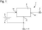
- the figure 1schematically represents the components of the smart battery 1.
- This batterycan be in the form of a battery or button cell as explained below to be placed in a battery housing of an electric instrument, such as a watch .
- This smart battery in the form of a button batteryis used to power the electronic elements of the electric instrument.
- the smart battery 1comprises at least one electronic circuit 8 for managing the supply voltage.
- the electronic circuitis connected by one of its connection pads 18 to an internal positive terminal 5 of the battery, which is defined as the cathode 5, and is also connected for its operation to an internal negative terminal 4 of the battery, which is defined as the anode.
- the internal negative terminal 4 of the batterycan be directly connected to an external negative terminal 2, while the output of the electronic circuit 8 can be directly connected to an external positive terminal 3.
- the power supply of an electric instrumentis supplied by the two external terminals 2 and 3 of the battery structure.
- the cathode 5 and the anode 4 of the batteryconsist of two chemical substances connected to one another with the interposition of a separator. These two chemicals react chemically in an electrolyte medium to create electrical energy supplied by the cathode 5 and the anode 4.
- These chemicalscan be made of lithium (Li) to define the anode 4 and manganese oxide ( MnO2) to define the cathode 5.
- the electronic circuit 8can comprise between the cathode 5 and the external positive terminal 3, a DC-DC converter, a processing or control unit connected to the converter, and an oscillator for controlling the DC-DC converter and the processing unit.
- the DC-DC convertermay advantageously be a Buck type converter, that is to say a converter lowering the supply voltage. This converter can be continuously in operation until the voltage supplied by the battery reaches an end of battery life (EOL) threshold. In this case, a direct connection between the external positive terminal 3 and the cathode 5 is performed by being controlled by the processing unit.
- the DC-DC converter of the electronic circuit 8can be configured according to a programming stored in a memory of the processing unit to be able to act as a voltage booster or a voltage step-down. It can also be configured to account for a charging or discharging mode of the battery. In the case of a battery charge, the DC-DC converter can instead be configured as a voltage booster for example.
- the electronic circuit 8Since the electronic circuit 8 must be arranged in a small battery 1, such as a button-type battery, the number of electronic components must be reduced.
- the size of the battery structuremay be of the order of 20 mm in diameter and 3.2 mm in thickness. It can be advantageously envisaged to integrate all the electronic components into a single integrated circuit. In this case, it is necessary use an oscillator with a built-in MEMS resonator or a fully integrated RC type oscillator.
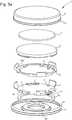
- This battery 1mainly comprises a first chemical substance 4 and a second chemical substance 5, which are connected to each other via a separator 6, and an electronic module 7, 8, 9, which comprises the electronic circuit 8 for managing the supply voltage.
- the electronic circuitis electrically connected to the first and second chemical substances.
- the first chemical substancedefines the anode 4, while the second chemical substance defines the cathode 5.
- the first and second chemical substancesreact chemically in a traditional electrolyte medium. This makes it possible to create an electric power supplied between the cathode 5, which is an internal positive terminal of the battery and the anode 4, which is an internal negative terminal of the battery.
- the first chemical substance 4is lithium (Li)
- the second chemical substance 5is manganese oxide (MnO2).
- the smart battery 1still includes a box 2, 3 enclosing all the components of the battery.
- This boxis composed of a bowl 3 and a lid 2, both of which are made of an electrically conductive material since the lid is the external negative terminal and the bowl is the external positive terminal of the battery.
- the lid 2may be generally cylindrical in shape with an upper part, which may be flat, and a cylindrical side wall, which is terminated by a peripheral rim 13 for fixing.
- the bowl 3comprises a bottom and an edge portion 14 to allow to be fixed in isolation to the lid in particular by a crimping operation.
- the lid 2is mounted on the bowl 3.
- the side wall with the peripheral edge 13 of the lid 2is inserted into the opening of the portion of the bowl. border 14 of the bowl 3.
- the componentsare held pressed between the inner surface of the upper part of the lid 2 and the bottom of the bowl 3.
- the edge portion 14is folded towards the peripheral edge 13 of the outer surface of the lid wall by the operation crimping for example with interposition of a seal shown in black on the figure 2a . Thanks to this seal, it electrically isolates the lid 2 of the bowl 3 while sealing the finished battery.
- the second chemical substance 5, which defines the cathode of the batteryis connected to the electronic circuit 8 as explained hereinafter.
- the connection of the second chemical substance with an input terminal of the electronic circuit 8constitutes the internal positive terminal of the smart battery 1.
- the electronic module carrying the electronic circuit 8is mounted on one side of the second chemical substance 5.
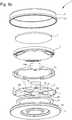
- This electronic modulecomprises a printed circuit board 7, on one side of which is mounted and connected at least the electronic circuit 8, which is encapsulated in an encapsulating material 9.
- the printed circuit board 7preferably has only a first face with a layer of conductive tracks 26, 27, 28 and an insulating layer on the layer of conductive tracks.
- a second insulating face of the printed circuit board 7is fixed or in contact with the second chemical substance 5.
- the electronic circuit 8is disposed in a central position of the printed circuit board 7.
- the electronic circuit 8is connected to at least a first electrical connection pad 23 by at least one first conductive track 26 on the first face of the printed circuit board 7.
- the first conductive track 26is connected to at least one output terminal of the electronic circuit 8.
- itcan be provided at least three first electrical connection pads 23 regularly spaced and describing portions of a circle.
- These first three connection pads 23are preferably identical and arranged midway between the center and the periphery of the printed circuit board 7.
- conductors 26to each connect the first corresponding connection pad 23.
- Each first connection pad 23is intended to come into contact with an electrical connection area 3a of the bowl 3, which defines the external positive terminal of the battery.
- This connection zone 3amay advantageously be of annular shape with a diameter equivalent to the diameter described by the first connection pads 23.
- This connection zone 3aextends towards the inside of the battery from the bottom of the bowl 3.
- the electronic circuit 8is further connected to at least a second electrical connection pad 17 by at least one second conductive track 27.
- This second electrical connection pad 17must be connected to the internal negative terminal, which is also the external negative terminal 2 as explained below.
- This external negative terminal of the coveris in direct contact with the first chemical substance 4, which defines the anode.
- the second conductive track 27is connected to at least one ground terminal of the electronic circuit 8.
- the three second connection pads 17are preferably each arranged on a corresponding first tab 7 'of the printed circuit board 7.
- the first three tabs 7'extend outward from the periphery, which may be circular, of the printed circuit board 7. Preferably, they may have a curvature for the connection of the second connection pads 17 to the inner surface of the wall of the lid 2.
- the first three tabs of identical shapeare arranged at the periphery being regularly spaced from each other, that is to say the center of each first tab is spaced 120 ° from the center of another first adjacent tab.
- the entire printed circuit board 7may be rigid or flexible. It can be envisaged to have the rigid fixing base of the printed circuit board 7, which carries the electronic circuit 8, while at least the first three tabs 7 'can be designed flexible.
- the printed circuit board 7is preferably a standard polyimide (PI) insulating substrate on which conductive traces, in particular copper tracks, are etched. An insulation or cover layer also of polyimide (PI) is deposited on the copper layer to isolate all the conductive tracks as shown by the dashed lines in particular at the figure 4a .
- PIpolyimide
- the electronic circuit 8is further connected to at least a third electrical connection pad 18 by at least one third conductive track 28.
- This third electrical connection pad 18must be connected to the internal positive terminal, which is in direct connection with the second chemical substance 5 corresponding to the cathode as explained below.
- the third conductive track 28is connected to at least one input terminal of the electronic circuit 8.
- the three third connection pads 18are preferably each disposed on a corresponding second tab 7 "of the printed circuit board 7.
- the three second tabs 7"extend outwardly from the circular periphery of the printed circuit board 7 before folding.
- Each second tabis bent 180 ° with respect to the base of the printed circuit board and fixed to the second face of the printed circuit board 7. After folding and fixing the second tabs, each third connection pad 18 is provided to electrically contact the second chemical substance 5.
- the three second tabs 7 "of identical shapeare arranged at the periphery being regularly spaced from each other, that is to say the center of each second tab is spaced 120 ° from the center of another adjacent tab
- the periphery of the printed circuit board 7thus comprises regularly spaced and alternately the first three tabs 7 'and the second three tabs 7 "for connection to the two chemical substances 4 and 5 with the second and third connection pads 17 and 18 .
- the three second tabs 7can be designed flexible to facilitate their folding and fixing.
- the fixing base of the printed circuit board 7can be rigid.
- the printed circuit board 7is mounted on an insulating support 10, which may be made of plastic material.
- the printed circuit board 7can be fixed for example by bonding to this insulating support 10, which is also fixed or bonded peripherally to the second chemical substance 5.
- This insulating supportcan be of generally annular shape with a central opening for the fixing the second face of the printed circuit board 7 to the second chemical substance 5.
- said insulating support 10has a lug 11 of cylindrical shape adapted to be inserted in a hole 12 of the printed circuit board 7. The hole is of diameter equal to or slightly greater than the diameter of the lug 11.
- the insulating support 10also has at the periphery at least one support heel 10a, and preferably three support heels 10a for supporting and fixing the first three tabs 7 '.
- the outer attachment surface of each support heel 10acorresponds to that of each first tab to be fixed.
- the outer surface of each bead 10ais bent to facilitate the attachment of each tab 7 'and allow to slightly bend and frictionally contact each second connection pad 17 on the inner surface of the lid wall 2 during assembly of the battery components. This frictional connection of the second connection pads is facilitated by the adaptation of the three beads 10a at the periphery of the insulating support 10.
- a sealing ring 15fixed to the bottom of the bowl 3 and which surrounds the annular connection zone 3a.
- the electronic circuit 8is first mounted on a first face of the printed circuit board 7, which comprises only one layer of conductive tracks 26, 27, 28 not intersecting and an insulating layer on the layer of conductive tracks.
- the electronic circuit 8is electrically connected in a conventional manner to the various conductive tracks before encapsulating the electronic circuit in an encapsulation material 9.
- the second tabs 7 "of the printed circuit boardare each folded by 180 ° and fixed on the second insulating face of the printed circuit board
- the third connection pads 18are thus on the side of the second face for connection with the second chemical substance 5, which defines the cathode.
- the first tabs 7 'of the printed circuit boardare curved and the second insulating faces of the first tabs are glued to the support heels 10a of complementary shape of the insulating support 10 while inserting the lug 11 of the support in the positioning hole 12 of the printed circuit board 7.
- the first insulated conductor track face of the printed circuit boardis disposed on the sealing ring 15, which is fixed on an inner side on the bottom of the bowl 3.
- This sealing ringmay be of glue material to allow to stick the first face of the printed circuit board on the sealing ring.
- the second chemical substance 5, which defines the cathode of the battery,is fixed on the insulating support 10 in contact with the second face of the printed circuit board 7 and the third connection pads 18. Before or after fixing the second substance 5 on the support 10, the separator 6 and the first chemical substance 4 are assembled on the second chemical substance 5.
- the cover 2is then mounted on the bowl 3 by pressing the support heels 10a, on which are fixed the first tabs 7 'externally carrying the second connection pads 17.
- An electrical contact including frictioncan be established between the inner surface of the wall of the cover 2 and the connection pads 17.
- the peripheral edge 13 for fixing the coveris inserted into the opening of the bowl by pressing the inner spacers components of the battery.
- the edge portion 14is folded towards the peripheral edge 13 of the outer surface of the wall of the lid. By performing this crimping operation, a seal is compressed between the edge portion 14 and the peripheral edge 13 to electrically isolate the lid 2 of the bowl 3 and seal the finished battery.
- connection to the two chemical substances of the electronic circuit for managing the supply voltage on the printed circuit boardcan be carried out in another way, for example by means of conductive connection tabs.
- the electronic circuitcan be placed on the periphery of the printed circuit board and a connection to the two chemical substances can be performed through conductive holes through the printed circuit board.
- the first connection padscan come into contact with an electrical connection area of the cover, which defines the external negative terminal of the battery according to the configuration of the connection arrangement of the electronic circuit.
- connection padscan directly contact the first chemical substance with the first tabs bent 180 ° and the second side of the printed circuit board attached to the first chemical substance.
- the connection area of the lidis of annular shape of diameter equivalent to the diameter described by the first connection pads.
- the second face of the printed circuit boardmay be attached or in contact with the first chemical substance, while the second chemical substance may be directly bonded to the external positive terminal of the cuvette.
Landscapes
- Engineering & Computer Science (AREA)
- Chemical & Material Sciences (AREA)
- Chemical Kinetics & Catalysis (AREA)
- Electrochemistry (AREA)
- General Chemical & Material Sciences (AREA)
- Manufacturing & Machinery (AREA)
- Microelectronics & Electronic Packaging (AREA)
- Power Engineering (AREA)
- Battery Mounting, Suspending (AREA)
- Primary Cells (AREA)
- Secondary Cells (AREA)
- Connection Of Batteries Or Terminals (AREA)
Description
Translated fromFrenchL'invention concerne une batterie intelligente, qui est munie d'un circuit électronique de gestion de la tension d'alimentation.The invention relates to a smart battery, which is provided with an electronic circuit for managing the supply voltage.
L'invention concerne également un procédé de fabrication d'une batterie intelligente.The invention also relates to a method of manufacturing a smart battery.
Pour la conception d'une batterie intelligente, un circuit électronique de gestion de la tension d'alimentation est intégré dans la structure de la batterie. Un tel circuit électronique peut comprendre un détecteur de fin de vie de batterie (EOL), un étage oscillateur, une unité de gestion de la puissance, voire une interface de communication. Le circuit électronique comprend également un convertisseur DC-DC entre la borne positive externe et la borne positive interne. Ce convertisseur DC-DC est mis en fonction de manière continue ou quand la tension d'alimentation est proche ou égale à un seuil de fin de vie de batterie (EOL). Il peut s'agir d'un convertisseur élévateur de tension (Boost) ou d'un convertisseur abaisseur de tension (Buck). Cela permet notamment de prolonger la durée de vie de la batterie tout en fournissant une tension suffisante d'alimentation au-dessus d'une limite minimale. Cette batterie peut aussi être du type rechargeable.For the design of a smart battery, an electronic circuit for managing the supply voltage is integrated into the structure of the battery. Such an electronic circuit may comprise a battery end of life detector (EOL), an oscillator stage, a power management unit, or even a communication interface. The electronic circuit also includes a DC-DC converter between the external positive terminal and the internal positive terminal. This DC-DC converter is operated continuously or when the supply voltage is close to or equal to an end of battery life (EOL) threshold. It can be a boost converter (Boost) or a buck converter. This allows in particular to extend the life of the battery while providing sufficient supply voltage above a minimum limit. This battery can also be of the rechargeable type.
Comme indiqué ci-devant, on peut citer le
Selon la figure 5B du brevet
Une autre batterie intelligente, qui pourrait être considérée comme l'état de la technique le plus proche de l'objet de l'invention, est décrite dans le brevet
L'invention a donc pour but de fournir une batterie intelligente, qui est munie d'un module électronique à circuit électronique de gestion de la tension d'alimentation et pouvant équiper une batterie d'une structure conventionnelle de petite dimension.The invention therefore aims to provide a smart battery, which is provided with an electronic module electronic circuit for managing the supply voltage and can equip a battery of a conventional structure of small size.
A cet effet, l'invention concerne une batterie intelligente munie d'un module électronique à circuit électronique de gestion de la tension d'alimentation, qui comprend les caractéristiques mentionnées dans la revendication indépendante 1.To this end, the invention relates to a smart battery provided with an electronic module with electronic circuit for managing the supply voltage, which comprises the characteristics mentioned in the
Des formes d'exécution particulières de la batterie intelligente sont définies dans les revendications dépendantes 2 à 24.Particular embodiments of the smart battery are defined in
Un avantage de la batterie intelligente réside dans le fait que toute l'électronique peut être intégrée dans une structure de batterie standard de petite dimension. La plaque à circuit imprimé portant le circuit électronique ne comprend des pistes conductrices que sur une première face et avec une seconde face isolante susceptible d'être fixée à l'une ou l'autre des substances chimiques.An advantage of the smart battery is that all electronics can be integrated into a standard small battery structure. The printed circuit board carrying the electronic circuit comprises conductive tracks only on a first face and with a second insulating face that can be attached to one or the other of the chemical substances.
Avantageusement le circuit électronique est relié depuis une borne de sortie à une ou plusieurs premières plages de connexion électrique sur la première face de la plaque à circuit imprimé par une ou plusieurs pistes conductrices. La ou les premières plages de connexion sont reliées directement de préférence à la cuvette comme borne positive externe de la batterie. Le circuit électronique est également relié aux deux substances chimiques par l'intermédiaire d'une ou plusieurs secondes et troisièmes plages de connexion par des pistes conductrices. De préférence, les secondes plages de connexion sont disposées sur des onglets fixés sur des talons supports d'un support isolant et les troisièmes plages de connexion sont disposées sur d'autres onglets pliés à 180° et connectés à la seconde substance chimique. Les secondes plages de connexion contactent une paroi intérieure du couvercle, qui est reliée à la première substance chimique.Advantageously, the electronic circuit is connected from an output terminal to one or more first electrical connection pads on the first face of the printed circuit board by one or more conductive tracks. The first connection pad or pads are directly connected to the bowl as an external positive terminal of the battery. The electronic circuit is also connected to the two chemical substances via one or more seconds and third pads by conductive tracks. Preferably, the second connection pads are arranged on tabs fixed on the support heels of an insulating support and the third pads are arranged on other tabs folded at 180 ° and connected to the second chemical substance. The second connection pads contact an inner wall of the lid, which is connected to the first chemical substance.
A cet effet, l'invention concerne un procédé de fabrication d'une batterie intelligente, qui comprend les caractéristiques mentionnées dans la revendication indépendante 25.To this end, the invention relates to a method of manufacturing a smart battery, which comprises the characteristics mentioned in the independent claim 25.
Des étapes particulières du procédé de fabrication sont définies dans les revendications dépendante 26 à 30.Particular steps of the manufacturing process are defined in the
Les buts, avantages et caractéristiques de la batterie intelligente munie d'un module électronique à circuit électronique de gestion de la tension d'alimentation, et de son procédé de fabrication apparaîtront mieux dans la description suivante sur la base d'au moins une forme d'exécution non limitative et illustrée par les dessins sur lesquels :
- la
figure 1 représente de manière simplifiée les composants de la batterie intelligente munie du circuit électronique de gestion de la tension d'alimentation selon l'invention, - les
figures 2a et2b représentent des vues en coupe diamétrale de la batterie intelligente selon l'invention une fois assemblée ou en vue en éclaté, - les
figures 3a et3b représentent des vues tridimensionnelles en éclaté de dessus et de dessous de la batterie intelligente selon l'invention, et - les
figures 4a et 4b représentent des vues tridimensionnelles de dessous et de dessus du module électronique de la batterie intelligente selon l'invention.
- the
figure 1 represents in simplified manner the components of the smart battery provided with the electronic circuit for managing the supply voltage according to the invention, - the
Figures 2a and2b represent diametrical sectional views of the smart battery according to the invention when assembled or in exploded view, - the
figures 3a and3b represent three-dimensional views exploded from above and below of the smart battery according to the invention, and - the
Figures 4a and 4b represent three-dimensional views from below and from above of the electronic module of the smart battery according to the invention.
Dans la description suivante, tous les composants intégrés de la batterie intelligente, qui sont bien connus d'un homme du métier dans ce domaine technique, ne sont décrits que de manière simplifiée.In the following description, all integrated components of the smart battery, which are well known to those skilled in this technical field, are described only in a simplified manner.
La
La batterie intelligente 1 comprend au moins un circuit électronique 8 de gestion de la tension d'alimentation. Le circuit électronique est relié par une de ses plages de connexion 18 à une borne positive interne 5 de la batterie, qui est définie comme la cathode 5, et est aussi relié pour son fonctionnement à une borne négative interne 4 de la batterie, qui est définie comme l'anode. La borne négative interne 4 de la batterie peut être directement reliée à une borne négative externe 2, alors que la sortie du circuit électronique 8 peut être reliée directement à une borne positive externe 3. L'alimentation électrique d'un instrument électrique est fournie par les deux bornes externes 2 et 3 de la structure de la batterie.The
La cathode 5 et l'anode 4 de la batterie sont constituées par deux substances chimiques liées l'une à l'autre avec interposition d'un séparateur. Ces deux substances chimiques réagissent chimiquement dans un milieu électrolyte pour créer une énergie électrique fournie par la cathode 5 et l'anode 4. Ces substances chimiques peuvent être constituées de Lithium (Li) pour définir l'anode 4 et d'oxyde de manganèse (MnO2) pour définir la cathode 5.The
Le circuit électronique 8 peut comprendre entre la cathode 5 et la borne positive externe 3, un convertisseur DC-DC, une unité de traitement ou contrôle reliée au convertisseur, et un oscillateur pour contrôler le convertisseur DC-DC et l'unité de traitement. De manière à économiser de l'énergie de la batterie, le convertisseur DC-DC peut être avantageusement un convertisseur du type Buck, c'est-à-dire un convertisseur abaissant la tension d'alimentation. Ce convertisseur peut être continuellement en fonction jusqu'à ce que la tension fournie par la batterie atteigne un seuil de fin de vie de pile (EOL). Dans ce cas de figure, une connexion directe entre la borne positive externe 3 et la cathode 5 est effectuée en étant commandé par l'unité de traitement.The
Le convertisseur DC-DC du circuit électronique 8 peut être configuré selon une programmation mémorisée dans une mémoire de l'unité de traitement pour pouvoir agir comme un élévateur de tension ou un abaisseur de tension. Il peut être configuré également pour tenir compte d'un mode de charge ou de décharge de la batterie. Dans le cas d'une charge de la batterie, le convertisseur DC-DC peut plutôt être configuré comme un élévateur de tension par exemple.The DC-DC converter of the
Comme le circuit électronique 8 doit être disposé dans une batterie 1 de petite dimension, telle qu'une batterie du type bouton, le nombre de composants électroniques doit être réduit. La taille de la structure de batterie peut être de l'ordre de 20 mm de diamètre et 3.2 mm d'épaisseur. Il peut être avantageusement envisagé d'intégrer tous les composants électroniques dans un unique circuit intégré. Dans ce cas de figure, il est nécessaire d'utiliser un oscillateur avec un résonateur du type MEMS intégré ou un oscillateur du type RC complètement intégré.Since the
La structure de la batterie intelligente 1 est maintenant décrite en référence aux
La première substance chimique définit l'anode 4, alors que la seconde substance chimique définit la cathode 5. Les première et seconde substances chimiques réagissent chimiquement dans un milieu électrolyte traditionnel. Cela permet de créer une énergie électrique fournie entre la cathode 5, qui est une borne positive interne de la batterie et l'anode 4, qui est une borne négative interne de la batterie. Avantageusement, la première substance chimique 4 est du Lithium (Li), alors que la seconde substance chimique 5 est de l'oxyde de manganèse (MnO2).The first chemical substance defines the
La batterie intelligente 1 comprend encore une boîte 2, 3 enfermant tous les composants de la batterie. Cette boîte est composée d'une cuvette 3 et d'un couvercle 2, qui sont tous les deux réalisés dans un matériau conducteur d'électricité étant donné que le couvercle est la borne négative externe et la cuvette est la borne positive externe de la batterie. Le couvercle 2 peut être de forme générale cylindrique avec une partie supérieure, qui peut être plane, et une paroi latérale cylindrique, qui est terminée par une bordure périphérique 13 de fixation. La cuvette 3 comprend un fond et une portion de bordure 14 pour permettre d'être fixée de manière isolée au couvercle notamment par une opération de sertissage.The
Une fois que les composants intérieurs de la batterie sont montés depuis le fond de la cuvette 3, le couvercle 2 est monté sur la cuvette 3. La paroi latérale avec la bordure périphérique 13 du couvercle 2 est insérée dans l'ouverture de la portion de bordure 14 de la cuvette 3. Les composants sont maintenus pressés entre la surface intérieure de la partie supérieure du couvercle 2 et le fond de la cuvette 3. Après cela, la portion de bordure 14 est repliée vers la bordure périphérique 13 de la surface extérieure de la paroi du couvercle par l'opération de sertissage par exemple avec interposition d'une garniture d'étanchéité représentée en noire sur la
La première substance chimique 4, qui définit l'anode de la batterie, vient directement en contact de la surface intérieure de la partie supérieure du couvercle 2, qui représente également la borne négative externe 2 de la batterie. Par contre, la seconde substance chimique 5, qui définit la cathode de la batterie, est reliée au circuit électronique 8 comme expliqué ci-après. La liaison de la seconde substance chimique avec une borne d'entrée du circuit électronique 8 constitue la borne positive interne de la batterie intelligente 1.The
Le module électronique portant le circuit électronique 8 est monté sur une face de la seconde substance chimique 5. Ce module électronique comprend une plaque à circuit imprimé 7, sur une face de laquelle est monté et connecté au moins le circuit électronique 8, qui est encapsulé dans un matériau d'encapsulation 9. La plaque à circuit imprimé 7 ne présente de préférence qu'une première face avec une couche de pistes conductrices 26, 27, 28 et une couche d'isolation sur la couche de pistes conductrices. Une seconde face isolante de la plaque à circuit imprimé 7 est fixée ou en contact de la seconde substance chimique 5. De préférence le circuit électronique 8 est disposé dans une position centrale de la plaque à circuit imprimé 7.The electronic module carrying the
Le circuit électronique 8 est relié à au moins une première plage de connexion électrique 23 par au moins une première piste conductrice 26 sur la première face de la plaque à circuit imprimé 7. La première piste conductrice 26 est reliée à au moins une borne de sortie du circuit électronique 8. De préférence, il peut être prévu au moins trois premières plages de connexion électrique 23 régulièrement espacées et décrivant des portions de cercle. Ces trois premières plages de connexion 23 sont de préférence identiques et disposées à mi-distance entre le centre et la périphérie de la plaque à circuit imprimé 7. De ce fait, il peut être également prévu, depuis le circuit électronique 8, trois premières pistes conductrices 26 pour relier chacune la première plage de connexion correspondante 23.The
Chaque première plage de connexion 23 est destinée à venir en contact d'une zone de connexion électrique 3a de la cuvette 3, qui définit la borne positive externe de la batterie. Cette zone de connexion 3a peut avantageusement être de forme annulaire de diamètre équivalent au diamètre décrit par les premières plages de connexion 23. Cette zone de connexion 3a s'étend vers l'intérieur de la batterie depuis le fond de la cuvette 3. Une fois que tous les composants sont montés entre le couvercle 2 et la cuvette 3, cette zone de connexion électrique 3a vient s'appuyer sur chaque première plage de connexion 23 pour établir une connexion électrique. Il peut aussi être prévu de souder les premières plages de connexion 23 sur la zone de connexion électrique 3a.Each
Le circuit électronique 8 est encore relié à au moins une seconde plage de connexion électrique 17 par au moins une seconde piste conductrice 27. Cette seconde plage de connexion électrique 17 doit être connectée à la borne négative interne, qui est aussi la borne négative externe 2 comme expliqué ci-après. Cette borne négative externe du couvercle est en contact direct avec la première substance chimique 4, qui définit l'anode. La seconde piste conductrice 27 est reliée à au moins une borne de masse du circuit électronique 8. De préférence, il est prévu trois secondes plages de connexion électrique 17 et trois secondes pistes conductrices 27 reliées chacune à une seconde plage de connexion 17 correspondante.The
Les trois secondes plages de connexion 17 sont de préférence disposées chacune sur un premier onglet 7' correspondant de la plaque à circuit imprimé 7. Les trois premiers onglets 7' s'étendent vers l'extérieur de la périphérie, qui peut être circulaire, de la plaque à circuit imprimé 7. De préférence, ils peuvent présenter une courbure pour la connexion des secondes plages de connexion 17 à la surface intérieure de la paroi du couvercle 2. Préférentiellement, les trois premiers onglets de forme identique sont disposés en périphérie en étant régulièrement espacés les uns des autres, c'est-à-dire le centre de chaque premier onglet est espacé de 120° du centre d'un autre premier onglet adjacent.The three
Il est à noter que toute la plaque à circuit imprimé 7 peut être rigide ou flexible. Il peut être envisagé d'avoir la base de fixation rigide de la plaque à circuit imprimé 7, qui porte le circuit électronique 8, alors qu'au moins les trois premiers onglets 7' peuvent être conçus flexibles. La plaque à circuit imprimé 7 est de préférence un substrat isolant en poly-imide (PI) standard sur lequel des pistes conductrices notamment en cuivre sont gravées. Une couche d'isolation ou de couverture également en poly-imide (PI) est déposée sur la couche de cuivre pour isoler toutes les pistes conductrices comme montré par les traits interrompus notamment à la
Le circuit électronique 8 est encore relié à au moins une troisième plage de connexion électrique 18 par au moins une troisième piste conductrice 28. Cette troisième plage de connexion électrique 18 doit être connectée à la borne positive interne, qui est en liaison directe avec la seconde substance chimique 5 correspondant à la cathode comme expliqué ci-après. La troisième piste conductrice 28 est reliée à au moins une borne d'entrée du circuit électronique 8. De préférence, il est prévu trois troisièmes plages de connexion électrique 18 et trois troisièmes pistes conductrices 28 reliées chacune à une troisième plage de connexion 18 correspondante.The
Les trois troisièmes plages de connexion 18 sont de préférence disposées chacune sur un second onglet 7" correspondant de la plaque à circuit imprimé 7. Les trois seconds onglets 7" s'étendent vers l'extérieur de la périphérie circulaire de la plaque à circuit imprimé 7 avant pliage. Chaque second onglet est plié de 180° par rapport à la base de fixation de la plaque à circuit imprimé et fixé sur la seconde face de la plaque à circuit imprimé 7. Après pliage et fixation des seconds onglets, chaque troisième plage de connexion 18 est prévue pour venir contacter électriquement la seconde substance chimique 5.The three
Préférentiellement, les trois seconds onglets 7" de forme identique sont disposés en périphérie en étant régulièrement espacés les uns des autres, c'est-à-dire le centre de chaque second onglet est espacé de 120° du centre d'un autre onglet adjacent. Chaque second onglet 7" est également disposé régulièrement espacé entre deux premiers onglets 7' voisins. La périphérie de la plaque à circuit imprimé 7 comprend donc régulièrement espacés et en alternance les trois premiers onglets 7' et les trois seconds onglets 7" pour la connexion aux deux substances chimiques 4 et 5 avec les secondes et troisièmes plages de connexion 17 et 18.Preferably, the three
Comme pour les trois premiers onglets 7', les trois seconds onglets 7" peuvent être conçus flexibles pour faciliter leur pliage et fixation. Par contre, la base de fixation de la plaque à circuit imprimé 7 peut être rigide.As for the first three tabs 7 ', the three
La plaque à circuit imprimé 7 est montée sur un support isolant 10, qui peut être réalisé en matériau plastique. La plaque à circuit imprimé 7 peut être fixée par exemple par collage à ce support isolant 10, qui est également fixé ou collé en périphérie à la seconde substance chimique 5. Ce support isolant peut être de forme générale annulaire avec ainsi une ouverture centrale pour la fixation de la seconde face de la plaque à circuit imprimé 7 à la seconde substance chimique 5. Pour le positionnement avant fixation de la plaque à circuit imprimé 7 sur le support, ledit support isolant 10 présente un ergot 11 de forme cylindrique adapté pour être inséré dans un trou 12 de la plaque à circuit imprimé 7. Le trou est de diamètre égal ou légèrement supérieur au diamètre de l'ergot 11.The printed
Le support isolant 10 présente encore en périphérie au moins un talon support 10a, et de préférence trois talons supports 10a pour supporter et fixer les trois premiers onglets 7'. La surface de fixation extérieure de chaque talon support 10a correspond à celle de chaque premier onglet à fixer. De préférence, la surface extérieure de chaque talon 10a est courbée pour faciliter la fixation de chaque onglet 7' et permettre de légèrement fléchir et contacter par frottement chaque seconde plage de connexion 17 sur la surface intérieure de la paroi du couvercle 2 lors du montage des composants de la batterie. Cette connexion par frottement des secondes plages de connexion est facilitée par l'adaptation des trois talons 10a en périphérie du support isolant 10.The insulating
Il peut encore être prévu un anneau d'étanchéité 15 fixé au fond de la cuvette 3 et qui entoure la zone annulaire de connexion 3a. La première face avec la couche isolante de la plaque à circuit imprimé 7 comprime l'anneau d'étanchéité pour venir connecter la zone de connexion 3a sur les premières plages de connexion 23.It can also be provided a
Il est expliqué maintenant les différentes étapes du procédé de fabrication de la batterie intelligente 1. Dans des étapes préliminaires, le circuit électronique 8 est tout d'abord monté sur une première face de la plaque à circuit imprimé 7, qui ne comprend qu'une couche de pistes conductrices 26, 27, 28 ne se croisant pas et une couche d'isolation sur la couche de pistes conductrices. Le circuit électronique 8 est relié électriquement de manière traditionnelle aux différentes pistes conductrices avant d'encapsuler le circuit électronique dans un matériau d'encapsulation 9. Les seconds onglets 7" de la plaque à circuit imprimé sont chacun pliés de 180° et fixés sur la seconde face isolante de la plaque à circuit imprimé. Les troisièmes plages de connexion 18 sont ainsi du côté de la seconde face pour une connexion avec la seconde substance chimique 5, qui définit la cathode.The different steps of the process for manufacturing the
Une fois le module électronique terminé, les premiers onglets 7' de la plaque à circuit imprimé sont courbés et les secondes faces isolantes des premiers onglets sont collées sur les talons supports 10a de forme complémentaire du support isolant 10 tout en insérant l'ergot 11 du support dans le trou 12 de positionnement de la plaque à circuit imprimé 7. La première face à pistes conductrices isolées de la plaque à circuit imprimé est disposée sur l'anneau d'étanchéité 15, qui est fixé d'un côté intérieur sur le fond de la cuvette 3. Cet anneau d'étanchéité peut être en matériau de colle pour permettre de coller la première face de la plaque à circuit imprimé sur l'anneau d'étanchéité.Once the electronic module is completed, the first tabs 7 'of the printed circuit board are curved and the second insulating faces of the first tabs are glued to the
La seconde substance chimique 5, qui définit la cathode de la batterie, est fixée sur le support isolant 10 en contact de la seconde face de la plaque à circuit imprimé 7 et des troisièmes plages de connexion 18. Avant ou après avoir fixé la seconde substance chimique 5 sur le support 10, le séparateur 6 et la première substance chimique 4 sont assemblés sur la seconde substance chimique 5.The
Le couvercle 2 est ensuite monté sur la cuvette 3 en pressant les talons supports 10a, sur lesquels sont fixés les premiers onglets 7' portant extérieurement les secondes plages de connexion 17. Un contact électrique notamment par frottement peut ainsi être établi entre la surface intérieure de la paroi du couvercle 2 et les plages de connexion 17. En étant guidé par les talons supports 10a, la bordure périphérique 13 de fixation du couvercle est inséré dans l'ouverture de la cuvette en pressant les composants intercalaires intérieurs de la batterie.The
Une fois le couvercle 2 positionné sur la cuvette 3, la portion de bordure 14 est repliée vers la bordure périphérique 13 de la surface extérieure de la paroi du couvercle. En effectuant cette opération de sertissage, une garniture d'étanchéité est comprimée entre la portion de bordure 14 et la bordure périphérique 13 afin d'isoler électriquement le couvercle 2 de la cuvette 3 et assurer l'étanchéité de la batterie terminée.Once the
A partir de la description qui vient d'être faite, plusieurs variantes de la batterie intelligente munie du module électronique à circuit électronique de gestion de la tension d'alimentation peuvent être conçues par l'homme du métier sans sortir du cadre de l'invention définie par les revendications. La connexion aux deux substances chimiques du circuit électronique de gestion de la tension d'alimentation sur la plaque à circuit imprimé peut être effectuée d'une autre manière par exemple au moyen de pattes conductrices de connexion. Le circuit électronique peut être placé en périphérie de la plaque à circuit imprimé et une connexion aux deux substances chimiques peut être effectuée par des trous conducteurs à travers la plaque à circuit imprimé. Les premières plages de connexion peuvent venir en contact d'une zone de connexion électrique du couvercle, qui définit la borne négative externe de la batterie en fonction de la configuration de l'agencement de connexion du circuit électronique. Les secondes plages de connexion peuvent venir contacter directement la première substance chimique avec les premiers onglets pliés de 180° et la seconde face de la plaque à circuit imprimé fixé sur la première substance chimique. La zone de connexion du couvercle est de forme annulaire de diamètre équivalent au diamètre décrit par les premières plages de connexion. La seconde face de la plaque à circuit imprimé peut être fixée ou en contact de la première substance chimique, alors que la seconde substance chimique peut être directement liée à la borne positive externe de la cuvette.From the description that has just been given, several variants of the smart battery provided with the electronic module electronic circuit for managing the supply voltage can be designed by those skilled in the art without departing from the scope of the invention defined by the claims. The connection to the two chemical substances of the electronic circuit for managing the supply voltage on the printed circuit board can be carried out in another way, for example by means of conductive connection tabs. The electronic circuit can be placed on the periphery of the printed circuit board and a connection to the two chemical substances can be performed through conductive holes through the printed circuit board. The first connection pads can come into contact with an electrical connection area of the cover, which defines the external negative terminal of the battery according to the configuration of the connection arrangement of the electronic circuit. The second connection pads can directly contact the first chemical substance with the first tabs bent 180 ° and the second side of the printed circuit board attached to the first chemical substance. The connection area of the lid is of annular shape of diameter equivalent to the diameter described by the first connection pads. The second face of the printed circuit board may be attached or in contact with the first chemical substance, while the second chemical substance may be directly bonded to the external positive terminal of the cuvette.
Claims (30)
- Smart battery (1), which includes an electronic module provided with an electronic circuit (8) for controlling the supply voltage, said electronic module being arranged in a case structure, which includes a cup (3) made of electrically conductive material and a cover (2) made of electrically conductive material, said cover (2) being fixed to the cup (3) by means of a sealing gasket, the cup defining an external positive terminal of the battery, whereas the cover defines an external negative terminal of the battery, the battery further including inside the case structure, a first chemical substance (4) as the anode, connected to a second chemical substance (5) as the cathode,
characterized in that the electronic module includes a printed circuit board (7) having a first face with a layer of conductive paths (26, 27, 28), the electronic circuit (8) being mounted and connected to conductive paths (26, 27, 28) on the first face, and a second insulating face fixed to or in contact with one of the chemical substances,
in that the electronic circuit (8) is connected, from an output terminal, to at least a first electrical connection pad (23) on the first face of the printed circuit board (7) by at least a first conductive path (26), the first electrical connection pad being connected directly to the cup (3) or to the cover (2),
in that the electronic circuit (8) is also connected to at least a second electrical connection pad (17) by at least a second conductive path (27), said second electrical connection pad being electrically connected to the first chemical substance defining an internal negative terminal, and which is connected to the cover, if the first connection pad is connected directly to the cup, and
in that the electronic circuit (8) is also connected to at least a third electrical connection pad (18) by at least a third conductive path (28), said third electrical connection pad being electrically connected to the second chemical substance defining an internal positive terminal, which is connected to the cup, if the first connection pad is connected directly to the cover. - Smart battery (1) according to claim 1,characterized in that an insulation layer is deposited on the layer of conductive paths (26, 27, 28), leaving access to the first electrical connection pad (23) for direct electrical connection to the cup (3) or to the cover (2).
- Smart battery (1) according to claim 2,characterized in that the printed circuit board (7) is flexible.
- Smart battery (1) according to claim 2,characterized in that the battery includes three first electrical connection pads (23).
- Smart battery (1) according to claim 4,characterized in that the three first electrical connection pads (23) are identical and disposed midway between the centre and the periphery of the circular printed circuit board (7).
- Smart battery (1) according to claim 5,characterized in that the three first electrical connection pads (23) are evenly spaced and describe portions of a circle.
- Smart battery (1) according to claim 6,characterized in that the three first electrical connection pads (23) come into contact with an electrical connection area (3a) of the cup (3) or of the cover (2), the electrical connection area (3a) being of annular shape and of equivalent diameter to the diameter described by the three first electrical connection pads (23).
- Smart battery (1) according to claim 1,characterized in that the electronic circuit (8) is disposed in a central portion of the printed circuit board (7).
- Smart battery (1) according to claim 1,characterized in that the second electrical connection pad (17) is disposed on a first tab (7') of the printed circuit board (7).
- Smart battery (1) according to claim 9,characterized in that the first tab (7') extends outwards from the periphery of the printed circuit board (7).
- Smart battery (1) according to claim 10,characterized in that the battery includes three second electrical connection pads (17), which are each disposed on a corresponding first tab (7') of the printed circuit board (7).
- Smart battery (1) according to claim 11,characterized in that the three identically-shaped first tabs (7') are disposed at the periphery of the circular printed circuit board (7), evenly spaced from each other, with the centre of each first tab separated by 120° from the centre of another adjacent first tab.
- Smart battery (1) according to claim 1,characterized in that the third electrical connection pad (18) is disposed on a second tab (7") of the printed circuit board (7).
- Smart battery (1) according to claim 13,characterized in that the second tab (7") extends outwards from the periphery of the printed circuit board (7).
- Smart battery (1) according to claim 14,characterized in that the battery includes three third electrical connection pads (18), which are each disposed on a corresponding second tab (7") of the printed circuit board (7).
- Smart battery (1) according to claim 15,characterized in that the three identically-shaped second tabs (7") are disposed at the periphery of the circular printed circuit board (7), evenly spaced from each other, with the centre of each second tab separated by 120° from the centre of another adjacent second tab.
- Smart battery (1) according to claim 16,characterized in that each second tab (7") is fixed to the second face of the printed circuit board (7), folded at 180° relative to a securing base of the printed circuit board, so as to electrically contact the second chemical substance.
- Smart battery (1) according to claim 1,characterized in that the battery includes three second electrical connection pads (17) each disposed on a corresponding first tab (7') of the printed circuit board (7) and three third electrical connection pads (18) each disposed on a corresponding second tab (7") of the printed circuit board, andin that the periphery of the printed circuit board (7) therefore includes, alternately and evenly spaced, the three first tabs (7') and the three second tabs (7") for connection to the two chemical substances (4, 5) with the second and third electrical connection pads (17, 18).
- Smart battery (1) according to claim 18,characterized in that the three first tabs (7') and the three second tabs (7") of the printed circuit board (7) are made of flexible material.
- Smart battery (1) according to claim 18,characterized in that the printed circuit board (7) is mounted on an insulating substrate (10) of annular shape, which is fixed to one of the chemical substances, andin that the second face of the printed circuit board (7) is fixed to one of the chemical substances through an opening in the insulating support (10).
- Smart battery (1) according to claim 20,characterized in that the insulating support (10) has at the periphery thereof three support heels (10a) for supporting and securing the three first tabs (7').
- Smart battery (1) according to claim 21,characterized in that the external securing surface of each support heel (10a) corresponds to that of each first tab to be secured, with one external surface of each heel (10a) being bent.
- Smart battery (1) according to claim 22,characterized in that the second electrical connection pads (17) are connected directly to the cover (2),in that the three third electrical connection pads (18), which are on the three second tabs (7") folded and fixed onto the second face of the printed circuit board (7), are electrically connected to the second chemical substance (5), andin that the three first electrical connection pads (23) are connected directly to the cup (3).
- Smart battery (1) according to claim 1,characterized in that the electronic circuit (8), which is mounted and connected to conductive paths (26, 27, 28) on the first face of the printed circuit board, is encapsulated in an encapsulation material, andin that the electronic circuit (8) includes a DC-DC converter, a processing unit connected to the converter, and an oscillator for controlling the DC-DC converter and the processing unit, said DC-DC converter being configured to step down the battery supply voltage until the voltage supplied by the battery reaches an end-of-life threshold.
- Method for manufacturing a smart battery (1) according to any of the preceding claims, the method including the steps consisting in:- mounting and electrically connecting the electronic circuit (8) on a first face of the printed circuit board (7), which includes a layer of conductive paths (26, 27, 28), at least a first conductive path (26) connecting an output terminal of the electronic circuit to at least a first electrical connection pad (23), at least a second conductive path (27) connecting an earth terminal of the electronic circuit to at least a second electrical connection pad (17), and at least a third conductive path (28) connecting an input terminal of the electronic circuit to at least a third electrical connection pad (18),- fixing or placing in contact a second insulating face of the printed circuit board (7) on one of the first and second chemical substances (4, 5), which are secured to each other,- electrically connecting the second electrical connection pad (17) to the first chemical substance (4),- electrically connecting the third electrical connection pad (18) to the second chemical substance (5),- placing the assembly of the electronic module and the first and second chemical substances in the cup (3),- mounting the cover (2), which includes a peripheral mounting edge (13), on the cup (3) by inserting said peripheral edge into an opening in the cup, the first electrical connection pad (23) being connected directly to the cup (3) or to the cover (2), and- folding down an edge portion (14) of the cup towards the peripheral edge (13) of the cover with the insertion of a sealing gasket to insulate the cover (2) from the cup (3).
- Manufacturing method according to claim 25, the method including, after mounting and electrically connecting the electronic circuit (8) on the first face of the printed circuit board (7), the steps of:- mounting the printed circuit board (7) on an insulating support (10) of annular shape,- fixing the insulating support to one of the chemical substances, and- fixing the second face of the printed circuit board (7) onto one of the chemical substances through an opening in the insulating support (10).
- Manufacturing method according to claim 26, wherein the second electrical connection pad (17) is disposed on a first tab (7'), which extends outwards at the periphery of the printed circuit board (7), and the third electrical connection pad (18) is disposed on a second tab (7") which extends outwards at the periphery of the printed circuit board (7),characterized in that before or after the electronic circuit (8) is mounted and electrically connected on the first face of the printed circuit board (7), the second tab is folded at 180° and fixed onto the second face of the printed circuit board, andin that the third electrical connection pad (18) comes into contact with the second chemical substance (5) when the second face of the printed circuit board is fixed to the second chemical substance.
- Manufacturing method according to claim 27, wherein the insulating support (10) includes at the periphery thereof at least one support heel (10a),characterized in that the second face of the first tab (7') is bent and bonded onto the complementary-shaped support heel (10a) of the insulating support.
- Manufacturing method according to claim 28, wherein three first tabs (7') are provided with three second connection pads (17), and three second tabs (7") with three third connection pads (18), the three first tabs and the three second tabs being evenly spaced and arranged alternately at the periphery of the printed circuit board, and wherein the insulating support (10) includes three support heels (10a) evenly spaced at the periphery,characterized in that before or after the electronic circuit (8) is mounted and electrically connected on the first face of the printed circuit board (7), the three second tabs (7") are folded at 180° and fixed onto the second face of the printed circuit board, andin that the second faces of the three first tabs (7') are bent and bonded onto the corresponding support heel (10a).
- Manufacturing method according to claim 29,characterized in that before the cover (2) is assembled, the first face of the printed circuit board (7) is placed on a sealing ring (15), which is fixed, on an inner side, to the base of the cup (3), andin that during assembly of the cover, an inner wall of the cover contacts the second connection pads (17), which are disposed on the first tabs (7') fixed to the support heels (10a), and an annular area (3a) of the base of the cup contacts the first electrical connection pad or pads (23).
Priority Applications (6)
| Application Number | Priority Date | Filing Date | Title |
|---|---|---|---|
| EP14170402.3AEP2950381B1 (en) | 2014-05-28 | 2014-05-28 | Smart battery with a circuit for managing the input voltage, and method for manufacturing the battery |
| US14/695,400US9728987B2 (en) | 2014-05-28 | 2015-04-24 | Smart battery with a supply voltage control circuit and method for manufacturing the battery |
| TW104113386ATWI670885B (en) | 2014-05-28 | 2015-04-27 | Smart battery with a supply voltage control circuit and method for manufacturing the battery |
| CN201510241194.9ACN105322243B (en) | 2014-05-28 | 2015-05-13 | Intelligent battery with source voltage control circuit and the method for manufacturing the battery |
| JP2015102475AJP6111286B2 (en) | 2014-05-28 | 2015-05-20 | Smart battery with supply voltage control circuit and method of manufacturing the battery |
| HK16109412.3AHK1222041B (en) | 2014-05-28 | 2016-08-08 | Smart battery with a supply voltage control circuit and method for manufacturing the battery |
Applications Claiming Priority (1)
| Application Number | Priority Date | Filing Date | Title |
|---|---|---|---|
| EP14170402.3AEP2950381B1 (en) | 2014-05-28 | 2014-05-28 | Smart battery with a circuit for managing the input voltage, and method for manufacturing the battery |
Publications (2)
| Publication Number | Publication Date |
|---|---|
| EP2950381A1 EP2950381A1 (en) | 2015-12-02 |
| EP2950381B1true EP2950381B1 (en) | 2016-12-14 |
Family
ID=50819661
Family Applications (1)
| Application Number | Title | Priority Date | Filing Date |
|---|---|---|---|
| EP14170402.3AActiveEP2950381B1 (en) | 2014-05-28 | 2014-05-28 | Smart battery with a circuit for managing the input voltage, and method for manufacturing the battery |
Country Status (5)
| Country | Link |
|---|---|
| US (1) | US9728987B2 (en) |
| EP (1) | EP2950381B1 (en) |
| JP (1) | JP6111286B2 (en) |
| CN (1) | CN105322243B (en) |
| TW (1) | TWI670885B (en) |
Families Citing this family (9)
| Publication number | Priority date | Publication date | Assignee | Title |
|---|---|---|---|---|
| CN114497782B (en) | 2015-09-08 | 2025-02-21 | 伏特技术有限公司 | Voltage regulating device and rechargeable battery having the same |
| US11527781B2 (en) | 2017-03-07 | 2022-12-13 | Volt Technology Limited | Battery with built-in voltage regulation device |
| CN108110201B (en)* | 2017-12-27 | 2021-08-24 | 惠州亿纬锂能股份有限公司 | Pole piece fixing mechanism and button cell |
| DE102018212710A1 (en)* | 2018-07-31 | 2020-02-06 | Robert Bosch Gmbh | Electrical energy store, device and / or vehicle and method for producing an electrical energy store |
| KR102787047B1 (en)* | 2019-05-10 | 2025-03-25 | 삼성에스디아이 주식회사 | Battery monitoring module |
| KR102505607B1 (en) | 2019-12-31 | 2023-03-03 | 삼성에스디아이 주식회사 | Battery pack |
| WO2021235243A1 (en)* | 2020-05-21 | 2021-11-25 | 株式会社村田製作所 | Battery pack and electronic device |
| DE102023111815B4 (en)* | 2023-05-05 | 2025-07-10 | esperta GmbH | Battery, in particular button cell, and method for its production |
| CN118040005B (en)* | 2024-03-22 | 2025-01-07 | 蜂巢能源科技股份有限公司 | Annular battery module assembly process |
Family Cites Families (18)
| Publication number | Priority date | Publication date | Assignee | Title |
|---|---|---|---|---|
| JP3344054B2 (en)* | 1993-12-29 | 2002-11-11 | ソニー株式会社 | Non-aqueous electrolyte secondary battery |
| JPH07272748A (en)* | 1994-03-31 | 1995-10-20 | Japan Storage Battery Co Ltd | Cell device |
| JP3018896B2 (en)* | 1994-04-01 | 2000-03-13 | 日本電池株式会社 | Battery device |
| JP2979963B2 (en)* | 1994-07-21 | 1999-11-22 | 日本電池株式会社 | Rechargeable battery |
| JPH09139235A (en)* | 1995-11-16 | 1997-05-27 | Japan Storage Battery Co Ltd | Battery device |
| US5637418A (en)* | 1996-02-08 | 1997-06-10 | Motorola, Inc. | Package for a flat electrochemical device |
| FR2748605B1 (en)* | 1996-05-07 | 1998-08-07 | Gerard Lemaire | METHOD FOR MANUFACTURING A BASIC BATTERY GENERATOR OR INTELLIGENT BATTERY |
| US6198250B1 (en) | 1998-04-02 | 2001-03-06 | The Procter & Gamble Company | Primary battery having a built-in controller to extend battery run time |
| US6074775A (en)* | 1998-04-02 | 2000-06-13 | The Procter & Gamble Company | Battery having a built-in controller |
| CA2305887A1 (en)* | 1999-04-21 | 2000-10-21 | Arthur Descombes | Protective circuit for battery |
| JP5064621B2 (en)* | 2001-09-04 | 2012-10-31 | 日立マクセルエナジー株式会社 | Information battery |
| US7705558B2 (en)* | 2003-10-31 | 2010-04-27 | Denovo Research, Llc | In situ rechargeable battery and charging stand |
| JP4499680B2 (en)* | 2005-03-30 | 2010-07-07 | 三星エスディアイ株式会社 | Cylindrical lithium ion secondary battery |
| TW200915698A (en)* | 2007-09-29 | 2009-04-01 | Acer Inc | Device to change the efficacy of charging or discharging based on the status of battery |
| US20090186169A1 (en)* | 2008-01-17 | 2009-07-23 | Harris Corporation | Three-dimensional liquid crystal polymer multilayer circuit board including battery and related methods |
| EP2301134B1 (en)* | 2008-07-11 | 2015-12-16 | EM Microelectronic-Marin SA | Power supply unit having a voltage converter |
| US9219288B2 (en)* | 2010-01-05 | 2015-12-22 | Samsung Sdi Co., Ltd. | Secondary battery |
| CN102117929A (en)* | 2010-01-05 | 2011-07-06 | 三星Sdi株式会社 | Secondary battery and smart card |
- 2014
- 2014-05-28EPEP14170402.3Apatent/EP2950381B1/enactiveActive
- 2015
- 2015-04-24USUS14/695,400patent/US9728987B2/enactiveActive
- 2015-04-27TWTW104113386Apatent/TWI670885B/enactive
- 2015-05-13CNCN201510241194.9Apatent/CN105322243B/enactiveActive
- 2015-05-20JPJP2015102475Apatent/JP6111286B2/enactiveActive
Non-Patent Citations (1)
| Title |
|---|
| None* |
Also Published As
| Publication number | Publication date |
|---|---|
| TW201611383A (en) | 2016-03-16 |
| CN105322243B (en) | 2017-08-22 |
| HK1222041A1 (en) | 2017-06-16 |
| JP6111286B2 (en) | 2017-04-05 |
| US9728987B2 (en) | 2017-08-08 |
| US20150349388A1 (en) | 2015-12-03 |
| TWI670885B (en) | 2019-09-01 |
| CN105322243A (en) | 2016-02-10 |
| EP2950381A1 (en) | 2015-12-02 |
| JP2015225857A (en) | 2015-12-14 |
Similar Documents
| Publication | Publication Date | Title |
|---|---|---|
| EP2950381B1 (en) | Smart battery with a circuit for managing the input voltage, and method for manufacturing the battery | |
| FR2504735A1 (en) | CONTACT DEVICE FOR GALVANIC BATTERY | |
| EP1416582B1 (en) | Portable electronic device with an electric connection inside the device case | |
| EP0948072B1 (en) | Prismatic rechargeable or primary cell with bobbin mounted coil | |
| TWI482333B (en) | Galvanic element for high stresses | |
| EP0958634B1 (en) | Method for making a smart battery generator cell | |
| FR2676309A1 (en) | BATTERY AND METHOD FOR ASSEMBLING MULTIPLE ELECTROCHEMICAL BATTERIES. | |
| FR2561447A1 (en) | LEAD ACCUMULATOR | |
| EP1213783A1 (en) | Battery with wound electrodes and heat dissipating means | |
| FR2773912A1 (en) | THIN TYPE WATERPROOF CELL ELEMENT, AND MANUFACTURING METHOD THEREOF | |
| CH713523B1 (en) | Portable electronic object such as a timepiece that can be worn on the wrist. | |
| EP0512906B1 (en) | Battery of nickel-hydrogen accumulators | |
| EP0863559A1 (en) | Thin type accumulator device comprising an electrochemical cell and electrical contact means | |
| EP1315051A1 (en) | Small electronic object that can be wrist worn | |
| WO2007068810A1 (en) | Fuel cell with current collectors integrated with the solid electrolyte and process for manufacturing such a fuel cell | |
| EP0186804A1 (en) | Wrist-mounted electronic device | |
| EP2131414B1 (en) | Connector, in particular for an energy storage device | |
| FR2692077A1 (en) | Accumulators with bipolar electrodes. | |
| CA2948387C (en) | Cutaneous device, in particular a pulse generator for electrical stimulation | |
| FR2479571A1 (en) | BATTERY TERMINAL STRUCTURE AND METHOD OF MOUNTING THE TERMINAL | |
| CN207010738U (en) | A kind of back splint battery | |
| FR2932023A1 (en) | Connector for energy storage device in motor vehicle, has armature partially drowned in plastic material of support, and electric power terminal mounted on armature, where armature is realized from steel sheet | |
| HK1222041B (en) | Smart battery with a supply voltage control circuit and method for manufacturing the battery | |
| EP3555950B1 (en) | Method for manufacturing an electronic object comprising a body and a porous-membrane battery | |
| CH719767B1 (en) | Button cell. |
Legal Events
| Date | Code | Title | Description |
|---|---|---|---|
| AK | Designated contracting states | Kind code of ref document:A1 Designated state(s):AL AT BE BG CH CY CZ DE DK EE ES FI FR GB GR HR HU IE IS IT LI LT LU LV MC MK MT NL NO PL PT RO RS SE SI SK SM TR | |
| AX | Request for extension of the european patent | Extension state:BA ME | |
| PUAI | Public reference made under article 153(3) epc to a published international application that has entered the european phase | Free format text:ORIGINAL CODE: 0009012 | |
| 17P | Request for examination filed | Effective date:20160602 | |
| RBV | Designated contracting states (corrected) | Designated state(s):AL AT BE BG CH CY CZ DE DK EE ES FI FR GB GR HR HU IE IS IT LI LT LU LV MC MK MT NL NO PL PT RO RS SE SI SK SM TR | |
| GRAP | Despatch of communication of intention to grant a patent | Free format text:ORIGINAL CODE: EPIDOSNIGR1 | |
| INTG | Intention to grant announced | Effective date:20160915 | |
| GRAS | Grant fee paid | Free format text:ORIGINAL CODE: EPIDOSNIGR3 | |
| GRAA | (expected) grant | Free format text:ORIGINAL CODE: 0009210 | |
| AK | Designated contracting states | Kind code of ref document:B1 Designated state(s):AL AT BE BG CH CY CZ DE DK EE ES FI FR GB GR HR HU IE IS IT LI LT LU LV MC MK MT NL NO PL PT RO RS SE SI SK SM TR | |
| REG | Reference to a national code | Ref country code:GB Ref legal event code:FG4D Free format text:NOT ENGLISH | |
| REG | Reference to a national code | Ref country code:CH Ref legal event code:EP | |
| REG | Reference to a national code | Ref country code:IE Ref legal event code:FG4D Free format text:LANGUAGE OF EP DOCUMENT: FRENCH | |
| REG | Reference to a national code | Ref country code:AT Ref legal event code:REF Ref document number:854327 Country of ref document:AT Kind code of ref document:T Effective date:20170115 | |
| REG | Reference to a national code | Ref country code:DE Ref legal event code:R096 Ref document number:602014005424 Country of ref document:DE | |
| PG25 | Lapsed in a contracting state [announced via postgrant information from national office to epo] | Ref country code:LV Free format text:LAPSE BECAUSE OF FAILURE TO SUBMIT A TRANSLATION OF THE DESCRIPTION OR TO PAY THE FEE WITHIN THE PRESCRIBED TIME-LIMIT Effective date:20161214 | |
| REG | Reference to a national code | Ref country code:CH Ref legal event code:NV Representative=s name:ICB INGENIEURS CONSEILS EN BREVETS SA, CH | |
| REG | Reference to a national code | Ref country code:LT Ref legal event code:MG4D | |
| REG | Reference to a national code | Ref country code:NL Ref legal event code:MP Effective date:20161214 | |
| REG | Reference to a national code | Ref country code:FR Ref legal event code:PLFP Year of fee payment:4 | |
| PG25 | Lapsed in a contracting state [announced via postgrant information from national office to epo] | Ref country code:SE Free format text:LAPSE BECAUSE OF FAILURE TO SUBMIT A TRANSLATION OF THE DESCRIPTION OR TO PAY THE FEE WITHIN THE PRESCRIBED TIME-LIMIT Effective date:20161214 Ref country code:GR Free format text:LAPSE BECAUSE OF FAILURE TO SUBMIT A TRANSLATION OF THE DESCRIPTION OR TO PAY THE FEE WITHIN THE PRESCRIBED TIME-LIMIT Effective date:20170315 Ref country code:LT Free format text:LAPSE BECAUSE OF FAILURE TO SUBMIT A TRANSLATION OF THE DESCRIPTION OR TO PAY THE FEE WITHIN THE PRESCRIBED TIME-LIMIT Effective date:20161214 Ref country code:NO Free format text:LAPSE BECAUSE OF FAILURE TO SUBMIT A TRANSLATION OF THE DESCRIPTION OR TO PAY THE FEE WITHIN THE PRESCRIBED TIME-LIMIT Effective date:20170314 | |
| REG | Reference to a national code | Ref country code:AT Ref legal event code:MK05 Ref document number:854327 Country of ref document:AT Kind code of ref document:T Effective date:20161214 | |
| PG25 | Lapsed in a contracting state [announced via postgrant information from national office to epo] | Ref country code:RS Free format text:LAPSE BECAUSE OF FAILURE TO SUBMIT A TRANSLATION OF THE DESCRIPTION OR TO PAY THE FEE WITHIN THE PRESCRIBED TIME-LIMIT Effective date:20161214 Ref country code:FI Free format text:LAPSE BECAUSE OF FAILURE TO SUBMIT A TRANSLATION OF THE DESCRIPTION OR TO PAY THE FEE WITHIN THE PRESCRIBED TIME-LIMIT Effective date:20161214 Ref country code:HR Free format text:LAPSE BECAUSE OF FAILURE TO SUBMIT A TRANSLATION OF THE DESCRIPTION OR TO PAY THE FEE WITHIN THE PRESCRIBED TIME-LIMIT Effective date:20161214 | |
| PG25 | Lapsed in a contracting state [announced via postgrant information from national office to epo] | Ref country code:NL Free format text:LAPSE BECAUSE OF FAILURE TO SUBMIT A TRANSLATION OF THE DESCRIPTION OR TO PAY THE FEE WITHIN THE PRESCRIBED TIME-LIMIT Effective date:20161214 | |
| PG25 | Lapsed in a contracting state [announced via postgrant information from national office to epo] | Ref country code:EE Free format text:LAPSE BECAUSE OF FAILURE TO SUBMIT A TRANSLATION OF THE DESCRIPTION OR TO PAY THE FEE WITHIN THE PRESCRIBED TIME-LIMIT Effective date:20161214 Ref country code:SK Free format text:LAPSE BECAUSE OF FAILURE TO SUBMIT A TRANSLATION OF THE DESCRIPTION OR TO PAY THE FEE WITHIN THE PRESCRIBED TIME-LIMIT Effective date:20161214 Ref country code:CZ Free format text:LAPSE BECAUSE OF FAILURE TO SUBMIT A TRANSLATION OF THE DESCRIPTION OR TO PAY THE FEE WITHIN THE PRESCRIBED TIME-LIMIT Effective date:20161214 Ref country code:IS Free format text:LAPSE BECAUSE OF FAILURE TO SUBMIT A TRANSLATION OF THE DESCRIPTION OR TO PAY THE FEE WITHIN THE PRESCRIBED TIME-LIMIT Effective date:20170414 Ref country code:RO Free format text:LAPSE BECAUSE OF FAILURE TO SUBMIT A TRANSLATION OF THE DESCRIPTION OR TO PAY THE FEE WITHIN THE PRESCRIBED TIME-LIMIT Effective date:20161214 | |
| PG25 | Lapsed in a contracting state [announced via postgrant information from national office to epo] | Ref country code:IT Free format text:LAPSE BECAUSE OF FAILURE TO SUBMIT A TRANSLATION OF THE DESCRIPTION OR TO PAY THE FEE WITHIN THE PRESCRIBED TIME-LIMIT Effective date:20161214 Ref country code:LU Free format text:LAPSE BECAUSE OF NON-PAYMENT OF DUE FEES Effective date:20170531 Ref country code:PT Free format text:LAPSE BECAUSE OF FAILURE TO SUBMIT A TRANSLATION OF THE DESCRIPTION OR TO PAY THE FEE WITHIN THE PRESCRIBED TIME-LIMIT Effective date:20170414 Ref country code:AT Free format text:LAPSE BECAUSE OF FAILURE TO SUBMIT A TRANSLATION OF THE DESCRIPTION OR TO PAY THE FEE WITHIN THE PRESCRIBED TIME-LIMIT Effective date:20161214 Ref country code:SM Free format text:LAPSE BECAUSE OF FAILURE TO SUBMIT A TRANSLATION OF THE DESCRIPTION OR TO PAY THE FEE WITHIN THE PRESCRIBED TIME-LIMIT Effective date:20161214 Ref country code:ES Free format text:LAPSE BECAUSE OF FAILURE TO SUBMIT A TRANSLATION OF THE DESCRIPTION OR TO PAY THE FEE WITHIN THE PRESCRIBED TIME-LIMIT Effective date:20161214 Ref country code:PL Free format text:LAPSE BECAUSE OF FAILURE TO SUBMIT A TRANSLATION OF THE DESCRIPTION OR TO PAY THE FEE WITHIN THE PRESCRIBED TIME-LIMIT Effective date:20161214 Ref country code:BG Free format text:LAPSE BECAUSE OF FAILURE TO SUBMIT A TRANSLATION OF THE DESCRIPTION OR TO PAY THE FEE WITHIN THE PRESCRIBED TIME-LIMIT Effective date:20170314 | |
| REG | Reference to a national code | Ref country code:DE Ref legal event code:R097 Ref document number:602014005424 Country of ref document:DE | |
| PLBE | No opposition filed within time limit | Free format text:ORIGINAL CODE: 0009261 | |
| STAA | Information on the status of an ep patent application or granted ep patent | Free format text:STATUS: NO OPPOSITION FILED WITHIN TIME LIMIT | |
| 26N | No opposition filed | Effective date:20170915 | |
| PG25 | Lapsed in a contracting state [announced via postgrant information from national office to epo] | Ref country code:DK Free format text:LAPSE BECAUSE OF FAILURE TO SUBMIT A TRANSLATION OF THE DESCRIPTION OR TO PAY THE FEE WITHIN THE PRESCRIBED TIME-LIMIT Effective date:20161214 | |
| PG25 | Lapsed in a contracting state [announced via postgrant information from national office to epo] | Ref country code:MC Free format text:LAPSE BECAUSE OF FAILURE TO SUBMIT A TRANSLATION OF THE DESCRIPTION OR TO PAY THE FEE WITHIN THE PRESCRIBED TIME-LIMIT Effective date:20161214 | |
| REG | Reference to a national code | Ref country code:IE Ref legal event code:MM4A | |
| PG25 | Lapsed in a contracting state [announced via postgrant information from national office to epo] | Ref country code:SI Free format text:LAPSE BECAUSE OF FAILURE TO SUBMIT A TRANSLATION OF THE DESCRIPTION OR TO PAY THE FEE WITHIN THE PRESCRIBED TIME-LIMIT Effective date:20161214 | |
| PG25 | Lapsed in a contracting state [announced via postgrant information from national office to epo] | Ref country code:LU Free format text:LAPSE BECAUSE OF NON-PAYMENT OF DUE FEES Effective date:20170528 | |
| REG | Reference to a national code | Ref country code:FR Ref legal event code:PLFP Year of fee payment:5 | |
| REG | Reference to a national code | Ref country code:BE Ref legal event code:MM Effective date:20170531 | |
| PG25 | Lapsed in a contracting state [announced via postgrant information from national office to epo] | Ref country code:IE Free format text:LAPSE BECAUSE OF NON-PAYMENT OF DUE FEES Effective date:20170528 | |
| PG25 | Lapsed in a contracting state [announced via postgrant information from national office to epo] | Ref country code:BE Free format text:LAPSE BECAUSE OF NON-PAYMENT OF DUE FEES Effective date:20170531 | |
| PG25 | Lapsed in a contracting state [announced via postgrant information from national office to epo] | Ref country code:MT Free format text:LAPSE BECAUSE OF FAILURE TO SUBMIT A TRANSLATION OF THE DESCRIPTION OR TO PAY THE FEE WITHIN THE PRESCRIBED TIME-LIMIT Effective date:20161214 | |
| GBPC | Gb: european patent ceased through non-payment of renewal fee | Effective date:20180528 | |
| PG25 | Lapsed in a contracting state [announced via postgrant information from national office to epo] | Ref country code:GB Free format text:LAPSE BECAUSE OF NON-PAYMENT OF DUE FEES Effective date:20180528 | |
| PG25 | Lapsed in a contracting state [announced via postgrant information from national office to epo] | Ref country code:HU Free format text:LAPSE BECAUSE OF FAILURE TO SUBMIT A TRANSLATION OF THE DESCRIPTION OR TO PAY THE FEE WITHIN THE PRESCRIBED TIME-LIMIT; INVALID AB INITIO Effective date:20140528 | |
| PG25 | Lapsed in a contracting state [announced via postgrant information from national office to epo] | Ref country code:CY Free format text:LAPSE BECAUSE OF FAILURE TO SUBMIT A TRANSLATION OF THE DESCRIPTION OR TO PAY THE FEE WITHIN THE PRESCRIBED TIME-LIMIT Effective date:20161214 | |
| PG25 | Lapsed in a contracting state [announced via postgrant information from national office to epo] | Ref country code:MK Free format text:LAPSE BECAUSE OF FAILURE TO SUBMIT A TRANSLATION OF THE DESCRIPTION OR TO PAY THE FEE WITHIN THE PRESCRIBED TIME-LIMIT Effective date:20161214 | |
| PG25 | Lapsed in a contracting state [announced via postgrant information from national office to epo] | Ref country code:TR Free format text:LAPSE BECAUSE OF FAILURE TO SUBMIT A TRANSLATION OF THE DESCRIPTION OR TO PAY THE FEE WITHIN THE PRESCRIBED TIME-LIMIT Effective date:20161214 | |
| PG25 | Lapsed in a contracting state [announced via postgrant information from national office to epo] | Ref country code:AL Free format text:LAPSE BECAUSE OF FAILURE TO SUBMIT A TRANSLATION OF THE DESCRIPTION OR TO PAY THE FEE WITHIN THE PRESCRIBED TIME-LIMIT Effective date:20161214 | |
| P01 | Opt-out of the competence of the unified patent court (upc) registered | Effective date:20230611 | |
| PGFP | Annual fee paid to national office [announced via postgrant information from national office to epo] | Ref country code:DE Payment date:20250423 Year of fee payment:12 | |
| PGFP | Annual fee paid to national office [announced via postgrant information from national office to epo] | Ref country code:FR Payment date:20250423 Year of fee payment:12 | |
| PGFP | Annual fee paid to national office [announced via postgrant information from national office to epo] | Ref country code:CH Payment date:20250601 Year of fee payment:12 |