EP2950147A1 - Environmental system including vaccum scavenge for an immersion lithography apparatus - Google Patents
Environmental system including vaccum scavenge for an immersion lithography apparatusDownload PDFInfo
- Publication number
- EP2950147A1 EP2950147A1EP15162756.9AEP15162756AEP2950147A1EP 2950147 A1EP2950147 A1EP 2950147A1EP 15162756 AEP15162756 AEP 15162756AEP 2950147 A1EP2950147 A1EP 2950147A1
- Authority
- EP
- European Patent Office
- Prior art keywords
- fluid
- gap
- stage
- exposure apparatus
- optical assembly
- Prior art date
- Legal status (The legal status is an assumption and is not a legal conclusion. Google has not performed a legal analysis and makes no representation as to the accuracy of the status listed.)
- Granted
Links
- 230000007613environmental effectEffects0.000titleclaimsabstractdescription64
- 238000000671immersion lithographyMethods0.000titledescription4
- 239000012530fluidSubstances0.000claimsabstractdescription317
- 238000007654immersionMethods0.000claimsabstractdescription139
- 230000003287optical effectEffects0.000claimsabstractdescription130
- 230000004888barrier functionEffects0.000claimsabstractdescription87
- 238000000034methodMethods0.000claimsdescription58
- 238000004519manufacturing processMethods0.000claimsdescription12
- XLYOFNOQVPJJNP-UHFFFAOYSA-NwaterSubstancesOXLYOFNOQVPJJNP-UHFFFAOYSA-N0.000claimsdescription10
- 238000005276aeratorMethods0.000claimsdescription3
- 230000002401inhibitory effectEffects0.000claims2
- 238000001914filtrationMethods0.000claims1
- 238000005086pumpingMethods0.000claims1
- 238000004891communicationMethods0.000abstractdescription25
- 238000005259measurementMethods0.000abstractdescription14
- 230000003094perturbing effectEffects0.000abstract1
- 235000012431wafersNutrition0.000description117
- 238000013461designMethods0.000description23
- 238000005286illuminationMethods0.000description15
- 230000008569processEffects0.000description14
- 239000000758substrateSubstances0.000description13
- 238000000206photolithographyMethods0.000description12
- 239000004065semiconductorSubstances0.000description8
- 238000001459lithographyMethods0.000description5
- 239000000203mixtureSubstances0.000description5
- 229920002120photoresistant polymerPolymers0.000description5
- 238000012545processingMethods0.000description5
- 230000000717retained effectEffects0.000description5
- 230000000712assemblyEffects0.000description4
- 238000000429assemblyMethods0.000description4
- 238000003384imaging methodMethods0.000description4
- 238000012546transferMethods0.000description4
- 238000006243chemical reactionMethods0.000description3
- 238000005530etchingMethods0.000description3
- 238000001704evaporationMethods0.000description3
- 239000000463materialSubstances0.000description3
- 239000003921oilSubstances0.000description3
- 238000012805post-processingMethods0.000description3
- 238000007781pre-processingMethods0.000description3
- 230000005855radiationEffects0.000description3
- 230000015572biosynthetic processEffects0.000description2
- 230000008859changeEffects0.000description2
- 239000000356contaminantSubstances0.000description2
- 230000000694effectsEffects0.000description2
- 229920001971elastomerPolymers0.000description2
- 230000008020evaporationEffects0.000description2
- 239000011521glassSubstances0.000description2
- 238000002347injectionMethods0.000description2
- 239000007924injectionSubstances0.000description2
- 239000007788liquidSubstances0.000description2
- 229920003023plasticPolymers0.000description2
- 239000004033plasticSubstances0.000description2
- 230000002000scavenging effectEffects0.000description2
- 239000004215Carbon black (E152)Substances0.000description1
- 229920002449FKMPolymers0.000description1
- 229920000459Nitrile rubberPolymers0.000description1
- WUKWITHWXAAZEY-UHFFFAOYSA-Lcalcium difluorideChemical compound[F-].[F-].[Ca+2]WUKWITHWXAAZEY-UHFFFAOYSA-L0.000description1
- 230000003749cleanlinessEffects0.000description1
- 238000010276constructionMethods0.000description1
- 239000010408filmSubstances0.000description1
- 239000010436fluoriteSubstances0.000description1
- NBVXSUQYWXRMNV-UHFFFAOYSA-NfluoromethaneChemical compoundFCNBVXSUQYWXRMNV-UHFFFAOYSA-N0.000description1
- 229930195733hydrocarbonNatural products0.000description1
- 150000002430hydrocarbonsChemical class0.000description1
- 238000009413insulationMethods0.000description1
- 238000005468ion implantationMethods0.000description1
- 150000002500ionsChemical class0.000description1
- 239000004973liquid crystal related substanceSubstances0.000description1
- QSHDDOUJBYECFT-UHFFFAOYSA-NmercuryChemical compound[Hg]QSHDDOUJBYECFT-UHFFFAOYSA-N0.000description1
- 229910052753mercuryInorganic materials0.000description1
- 229910052751metalInorganic materials0.000description1
- 239000002184metalSubstances0.000description1
- 238000012544monitoring processMethods0.000description1
- 230000003647oxidationEffects0.000description1
- 238000007254oxidation reactionMethods0.000description1
- 238000012858packaging processMethods0.000description1
- 238000009428plumbingMethods0.000description1
- 229920001084poly(chloroprene)Polymers0.000description1
- 230000036316preloadEffects0.000description1
- 239000010453quartzSubstances0.000description1
- 238000011084recoveryMethods0.000description1
- 239000012858resilient materialSubstances0.000description1
- VYPSYNLAJGMNEJ-UHFFFAOYSA-Nsilicon dioxideInorganic materialsO=[Si]=OVYPSYNLAJGMNEJ-UHFFFAOYSA-N0.000description1
- 239000002210silicon-based materialSubstances0.000description1
- 229910001220stainless steelInorganic materials0.000description1
- 239000010935stainless steelSubstances0.000description1
- 230000003068static effectEffects0.000description1
- 239000010409thin filmSubstances0.000description1
- 238000007740vapor depositionMethods0.000description1
- 238000009834vaporizationMethods0.000description1
- 230000008016vaporizationEffects0.000description1
Images


Classifications
- G—PHYSICS
- G03—PHOTOGRAPHY; CINEMATOGRAPHY; ANALOGOUS TECHNIQUES USING WAVES OTHER THAN OPTICAL WAVES; ELECTROGRAPHY; HOLOGRAPHY
- G03F—PHOTOMECHANICAL PRODUCTION OF TEXTURED OR PATTERNED SURFACES, e.g. FOR PRINTING, FOR PROCESSING OF SEMICONDUCTOR DEVICES; MATERIALS THEREFOR; ORIGINALS THEREFOR; APPARATUS SPECIALLY ADAPTED THEREFOR
- G03F7/00—Photomechanical, e.g. photolithographic, production of textured or patterned surfaces, e.g. printing surfaces; Materials therefor, e.g. comprising photoresists; Apparatus specially adapted therefor
- G03F7/70—Microphotolithographic exposure; Apparatus therefor
- G03F7/708—Construction of apparatus, e.g. environment aspects, hygiene aspects or materials
- G03F7/70858—Environment aspects, e.g. pressure of beam-path gas, temperature
- G03F7/70866—Environment aspects, e.g. pressure of beam-path gas, temperature of mask or workpiece
- G03F7/70875—Temperature, e.g. temperature control of masks or workpieces via control of stage temperature
- G—PHYSICS
- G03—PHOTOGRAPHY; CINEMATOGRAPHY; ANALOGOUS TECHNIQUES USING WAVES OTHER THAN OPTICAL WAVES; ELECTROGRAPHY; HOLOGRAPHY
- G03F—PHOTOMECHANICAL PRODUCTION OF TEXTURED OR PATTERNED SURFACES, e.g. FOR PRINTING, FOR PROCESSING OF SEMICONDUCTOR DEVICES; MATERIALS THEREFOR; ORIGINALS THEREFOR; APPARATUS SPECIALLY ADAPTED THEREFOR
- G03F7/00—Photomechanical, e.g. photolithographic, production of textured or patterned surfaces, e.g. printing surfaces; Materials therefor, e.g. comprising photoresists; Apparatus specially adapted therefor
- G03F7/20—Exposure; Apparatus therefor
- G03F7/2041—Exposure; Apparatus therefor in the presence of a fluid, e.g. immersion; using fluid cooling means
- G—PHYSICS
- G03—PHOTOGRAPHY; CINEMATOGRAPHY; ANALOGOUS TECHNIQUES USING WAVES OTHER THAN OPTICAL WAVES; ELECTROGRAPHY; HOLOGRAPHY
- G03F—PHOTOMECHANICAL PRODUCTION OF TEXTURED OR PATTERNED SURFACES, e.g. FOR PRINTING, FOR PROCESSING OF SEMICONDUCTOR DEVICES; MATERIALS THEREFOR; ORIGINALS THEREFOR; APPARATUS SPECIALLY ADAPTED THEREFOR
- G03F7/00—Photomechanical, e.g. photolithographic, production of textured or patterned surfaces, e.g. printing surfaces; Materials therefor, e.g. comprising photoresists; Apparatus specially adapted therefor
- G03F7/70—Microphotolithographic exposure; Apparatus therefor
- G03F7/70216—Mask projection systems
- G03F7/70341—Details of immersion lithography aspects, e.g. exposure media or control of immersion liquid supply
- G—PHYSICS
- G03—PHOTOGRAPHY; CINEMATOGRAPHY; ANALOGOUS TECHNIQUES USING WAVES OTHER THAN OPTICAL WAVES; ELECTROGRAPHY; HOLOGRAPHY
- G03F—PHOTOMECHANICAL PRODUCTION OF TEXTURED OR PATTERNED SURFACES, e.g. FOR PRINTING, FOR PROCESSING OF SEMICONDUCTOR DEVICES; MATERIALS THEREFOR; ORIGINALS THEREFOR; APPARATUS SPECIALLY ADAPTED THEREFOR
- G03F7/00—Photomechanical, e.g. photolithographic, production of textured or patterned surfaces, e.g. printing surfaces; Materials therefor, e.g. comprising photoresists; Apparatus specially adapted therefor
- G03F7/70—Microphotolithographic exposure; Apparatus therefor
- G03F7/70691—Handling of masks or workpieces
- G03F7/70775—Position control, e.g. interferometers or encoders for determining the stage position
- G—PHYSICS
- G03—PHOTOGRAPHY; CINEMATOGRAPHY; ANALOGOUS TECHNIQUES USING WAVES OTHER THAN OPTICAL WAVES; ELECTROGRAPHY; HOLOGRAPHY
- G03F—PHOTOMECHANICAL PRODUCTION OF TEXTURED OR PATTERNED SURFACES, e.g. FOR PRINTING, FOR PROCESSING OF SEMICONDUCTOR DEVICES; MATERIALS THEREFOR; ORIGINALS THEREFOR; APPARATUS SPECIALLY ADAPTED THEREFOR
- G03F7/00—Photomechanical, e.g. photolithographic, production of textured or patterned surfaces, e.g. printing surfaces; Materials therefor, e.g. comprising photoresists; Apparatus specially adapted therefor
- G03F7/70—Microphotolithographic exposure; Apparatus therefor
- G03F7/708—Construction of apparatus, e.g. environment aspects, hygiene aspects or materials
- G03F7/70808—Construction details, e.g. housing, load-lock, seals or windows for passing light in or out of apparatus
- G03F7/70816—Bearings
- G—PHYSICS
- G03—PHOTOGRAPHY; CINEMATOGRAPHY; ANALOGOUS TECHNIQUES USING WAVES OTHER THAN OPTICAL WAVES; ELECTROGRAPHY; HOLOGRAPHY
- G03F—PHOTOMECHANICAL PRODUCTION OF TEXTURED OR PATTERNED SURFACES, e.g. FOR PRINTING, FOR PROCESSING OF SEMICONDUCTOR DEVICES; MATERIALS THEREFOR; ORIGINALS THEREFOR; APPARATUS SPECIALLY ADAPTED THEREFOR
- G03F7/00—Photomechanical, e.g. photolithographic, production of textured or patterned surfaces, e.g. printing surfaces; Materials therefor, e.g. comprising photoresists; Apparatus specially adapted therefor
- G03F7/70—Microphotolithographic exposure; Apparatus therefor
- G03F7/708—Construction of apparatus, e.g. environment aspects, hygiene aspects or materials
- G03F7/70858—Environment aspects, e.g. pressure of beam-path gas, temperature
- G03F7/70866—Environment aspects, e.g. pressure of beam-path gas, temperature of mask or workpiece
- G—PHYSICS
- G03—PHOTOGRAPHY; CINEMATOGRAPHY; ANALOGOUS TECHNIQUES USING WAVES OTHER THAN OPTICAL WAVES; ELECTROGRAPHY; HOLOGRAPHY
- G03F—PHOTOMECHANICAL PRODUCTION OF TEXTURED OR PATTERNED SURFACES, e.g. FOR PRINTING, FOR PROCESSING OF SEMICONDUCTOR DEVICES; MATERIALS THEREFOR; ORIGINALS THEREFOR; APPARATUS SPECIALLY ADAPTED THEREFOR
- G03F7/00—Photomechanical, e.g. photolithographic, production of textured or patterned surfaces, e.g. printing surfaces; Materials therefor, e.g. comprising photoresists; Apparatus specially adapted therefor
- G03F7/70—Microphotolithographic exposure; Apparatus therefor
- G03F7/708—Construction of apparatus, e.g. environment aspects, hygiene aspects or materials
- G03F7/70858—Environment aspects, e.g. pressure of beam-path gas, temperature
- G03F7/709—Vibration, e.g. vibration detection, compensation, suppression or isolation
- H—ELECTRICITY
- H01—ELECTRIC ELEMENTS
- H01L—SEMICONDUCTOR DEVICES NOT COVERED BY CLASS H10
- H01L21/00—Processes or apparatus adapted for the manufacture or treatment of semiconductor or solid state devices or of parts thereof
- H01L21/02—Manufacture or treatment of semiconductor devices or of parts thereof
- H01L21/027—Making masks on semiconductor bodies for further photolithographic processing not provided for in group H01L21/18 or H01L21/34
- H01L21/0271—Making masks on semiconductor bodies for further photolithographic processing not provided for in group H01L21/18 or H01L21/34 comprising organic layers
- H01L21/0273—Making masks on semiconductor bodies for further photolithographic processing not provided for in group H01L21/18 or H01L21/34 comprising organic layers characterised by the treatment of photoresist layers
- H01L21/0274—Photolithographic processes
Definitions
- Provisional Application Serial No. 60/462,112filed on April 10, 2003 and entitled "VACUUM RING SYSTEM AND WICK RING SYSTEM FOR IMMERSION LITHOGRAPHY METHOD AND DEVICE FOR CONTROLLING THERMAL DISTORTION IN ELEMENTS OF A LITHOGRAPHY STSTEM” and Provisional Application Serial No. 60/484,476 filed on July 1, 2003 and entitled “FLUID CONTROL SYSTEM FOR IMMERSION LITHOGRAPHY TOOL".
- provisional Application Serial Nos. 60/462,112 and 60/484,476are incorporated herein by reference.
- Lithography exposure apparatusesare commonly used to transfer images from a reticle onto a semiconductor wafer during semiconductor processing.
- a typical exposure apparatusincludes an illumination source, a reticle stage assembly that positions a reticle, an optical assembly, a wafer stage assembly that positions a semiconductor wafer, and a measurement system that precisely monitors the position of the reticle and the wafer.
- Immersion lithography systemsutilize a layer of immersion fluid that completely fills a gap between the optical assembly and the wafer.
- the waferis moved rapidly in a typical lithography system and it would be expected to carry the immersion fluid away from the gap.
- This immersion fluid that escapes from the gapcan interfere with the operation of other components of the lithography system.
- the immersion fluid and its vaporcan interfere with the measurement system that monitors the position of the wafer.
- the present inventionis directed to an environmental system for controlling an environment in a gap between an optical assembly and a device that is retained by a device stage.
- the environmental systemincludes a fluid barrier and an immersion fluid system.
- the fluid barrieris positioned near the device and encircles the gap.
- the immersion fluid systemdelivers an immersion fluid that fills the gap.
- the immersion fluid systemcollects the immersion fluid that is directly between the fluid barrier and at least one of the device and the device stage.
- the fluid barrierincludes a scavenge inlet that is positioned near the device, and the immersion fluid system includes a low pressure source that is in fluid communication with the scavenge inlet. Additionally, the fluid barrier can confine and contain the immersion fluid and any of the vapor from the immersion fluid in the area near the gap.
- the environmental systemincludes a bearing fluid source that directs a bearing fluid between the fluid barrier and the device to support the fluid barrier relative to the device.
- the fluid barrierincludes a bearing outlet that is positioned near the device. Further, the bearing outlet is in fluid communication with the bearing fluid source.
- the environmental systemcan include a pressure equalizer that allows the pressure in the gap to be approximately equal to the pressure outside the fluid barrier.
- the pressure equalizeris a channel that extends through the fluid barrier.
- the device stagecan include a stage surface that is in approximately the same plane as a device exposed surface of the device.
- the device stagecan include a device holder that retains the device, a guard that defines the stage surface, and a mover assembly that moves one of the device holder and the guard so that the device exposed surface is approximately in the same plane as the stage surface.
- the mover assemblymoves the guard relative to the device and the device holder. In another embodiment, the mover assembly moves the device holder and the device relative to the guard.
- the present inventionis also directed to an exposure apparatus, a wafer, a device, a method for controlling an environment in a gap, a method for making an exposure apparatus, a method for making a device, and a method for manufacturing a wafer.
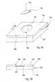
- FIG 1is a schematic illustration of a precision assembly, namely an exposure apparatus 10 having features of the present invention.
- the exposure apparatus 10includes an apparatus frame 12, an illumination system 14 (irradiation apparatus), an optical assembly 16, a reticle stage assembly 18, a device stage assembly 20, a measurement system 22, a control system 24, and a fluid environmental system 26.
- the design of the components of the exposure apparatus 10can be varied to suit the design requirements of the exposure apparatus 10.
- a number of Figuresinclude an orientation system that illustrates an X axis, a Y axis that is orthogonal to the X axis, and a Z axis that is orthogonal to the X and Y axes. It should be noted that these axes can also be referred to as the first, second and third axes.
- the exposure apparatus 10is particularly useful as a lithographic device that transfers a pattern (not shown) of an integrated circuit from a reticle 28 onto a semiconductor wafer 30 (illustrated in phantom).
- the wafer 30is also referred to generally as a device or work piece.
- the exposure apparatus 10mounts to a mounting base 32, e.g., the ground, a base, or floor or some other supporting structure.
- the exposure apparatus 10can be used as a scanning type photolithography system that exposes the pattern from the reticle 28 onto the wafer 30 with the reticle 28 and the wafer 30 moving synchronously.
- a scanning type lithographic devicethe reticle 28 is moved perpendicularly to an optical axis of the optical assembly 16 by the reticle stage assembly 18 and the wafer 30 is moved perpendicularly to the optical axis of the optical assembly 16 by the wafer stage assembly 20. Scanning of the reticle 28 and the wafer 30 occurs while the reticle 28 and the wafer 30 are moving synchronously.
- the exposure apparatus 10can be a step-and-repeat type photolithography system that exposes the reticle 28 while the reticle 28 and the wafer 30 are stationary.
- the wafer 30is in a constant position relative to the reticle 28 and the optical assembly 16 during the exposure of an individual field.
- the wafer 30is consecutively moved with the wafer stage assembly 20 perpendicularly to the optical axis of the optical assembly 16 so that the next field of the wafer 30 is brought into position relative to the optical assembly 16 and the reticle 28 for exposure.
- the images on the reticle 28are sequentially exposed onto the fields of the wafer 30, and then the next field of the wafer 30 is brought into position relative to the optical assembly 16 and the reticle 28.
- the use of the exposure apparatus 10 provided hereinis not limited to a photolithography system for semiconductor manufacturing.
- the exposure apparatus 10, for example,can be used as an LCD photolithography system that exposes a liquid crystal display device pattern onto a rectangular glass plate or a photolithography system for manufacturing a thin film magnetic head.
- the apparatus frame 12supports the components of the exposure apparatus 10.
- the apparatus frame 12 illustrated in Figure 1supports the reticle stage assembly 18, the wafer stage assembly 20, the optical assembly 16 and the illumination system 14 above the mounting base 32.
- the illumination system 14includes an illumination source 34 and an illumination optical assembly 36.
- the illumination source 34emits a beam (irradiation) of light energy.
- the illumination optical assembly 36guides the beam of light energy from the illumination source 34 to the optical assembly 16.
- the beamilluminates selectively different portions of the reticle 28 and exposes the wafer 30.
- the illumination source 34is illustrated as being supported above the reticle stage assembly 18. Typically, however, the illumination source 34 is secured to one of the sides of the apparatus frame 12 and the energy beam from the illumination source 34 is directed to above the reticle stage assembly 18 with the illumination optical assembly 36.
- the illumination source 34can be a light source such as a mercury g-line source (436 nm) or i-line source (365 nm), a KrF excimer laser (248 nm), an ArF excimer laser (193 nm) or a F 2 laser (157 nm).
- the optical assembly 16projects and/or focuses the light passing through the reticle 28 to the wafer 30. Depending upon the design of the exposure apparatus 10, the optical assembly 16 can magnify or reduce the image illuminated on the reticle 28. It could also be a 1x magnification system.
- optical assembly 16When far ultra-violet radiation such as from the excimer laser is used, glass materials such as quartz and fluorite that transmit far ultra-violet rays can be used in the optical assembly 16.
- the optical assembly 16can be either catadioptric or refractive.
- the catadioptric type optical systemcan be considered.
- the catadioptric type of optical systeminclude the disclosure Japan Patent Application Disclosure No. 8-171054 published in the Official Gazette for Laid-Open Patent Applications and its counterpart U.S. Patent No, 5,668,672 , as well as Japan Patent Application Disclosure No. 10-20195 and its counterpart U.S. Patent No. 5,835,275 .
- the reflecting optical devicecan be a catadioptric optical system incorporating a beam splitter and concave mirror.
- Japan Patent Application Disclosure No. 8-334695published in the Official Gazette for Laid-Open Patent Applications and its counterpart U.S. Patent No.
- the optical assembly 16is secured to the apparatus frame 12 with one or more optical mount isolators 37.
- the optical mount isolators 37inhibit vibration of the apparatus frame 12 from causing vibration to the optical assembly 16.
- Each optical mount isolator 37can include a pneumatic cylinder (not shown) that isolates vibration and an actuator (not shown) that isolates vibration and controls the position with at least two degrees of motion.
- Suitable optical mount isolators 37are sold by Integrated Dynamics Engineering, located in Wobum, MA.
- two spaced apart optical mount isolators 37are shown as being used to secure the optical assembly 16 to the apparatus frame 12.
- three spaced apart optical mount isolators 37can be used to kinematically secure the optical assembly 16 to the apparatus frame 12.
- the reticle stage assembly 18holds and positions the reticle 28 relative to the optical assembly 16 and the wafer 30.
- the reticle stage assembly 18includes a reticle stage 38 that retains the reticle 28 and a reticle stage mover assembly 40 that moves and positions the reticle stage 38 and reticle 28.
- the device stage assembly 20holds and positions the wafer 30 with respect to the projected image of the illuminated portions of the reticle 28.
- the device stage assembly 20includes a device stage 42 that retains the wafer 30, a device stage base 43 that supports and guides the device stage 42, and a device stage mover assembly 44 that moves and positions the device stage 42 and the wafer 28 relative to the optical assembly 16 and the device stage base 43.
- the device stage 42is described in more detail below.
- Each stage mover assembly 40, 44can move the respective stage 38, 42 with three degrees of freedom, less than three degrees of freedom, or more than three degrees of freedom.
- each stage mover assembly 40, 44can move the respective stage 38, 42 with one, two, three, four, five or six degrees of freedom.
- the reticle stage mover assembly 40 and the device stage mover assembly 44can each include one or more movers, such as rotary motors, voice coil motors, linear motors utilizing a Lorentz force to generate drive force, electromagnetic movers, planar motors, or some other force movers.
- one of the stagescould be driven by a planar motor, which drives the stage by an electromagnetic force generated by a magnet unit having two-dimensionally arranged magnets and an armature coil unit having two-dimensionally arranged coils in facing positions.
- a planar motorwhich drives the stage by an electromagnetic force generated by a magnet unit having two-dimensionally arranged magnets and an armature coil unit having two-dimensionally arranged coils in facing positions.
- either the magnet unit or the armature coil unitis connected to the stage base and the other unit is mounted on the moving plane side of the stage.
- reaction forces generated by the wafer (substrate) stage motioncan be mechanically transferred to the floor (ground) by use of a frame member as described in US Patent No. 5,528,100 and published Japanese Patent Application Disclosure No. 8-136475 .
- reaction forces generated by the reticle (mask) stage motioncan be mechanically transferred to the floor (ground) by use of a frame member as described in US Patent No. 5,874,820 and published Japanese Patent Application Disclosure No. 8-330224 .
- the disclosures in US Patent Numbers 5,528,100 and 5,874,820 and Japanese Patent Application Disclosure No. 8-330224are incorporated herein by reference.
- the measurement system 22monitors movement of the reticle 28 and the wafer 30 relative to the optical assembly 16 or some other reference. With this information, the control system 24 can control the reticle stage assembly 18 to precisely position the reticle 28 and the device stage assembly 20 to precisely position the wafer 30.
- the design of the measurement system 22can vary. For example, the measurement system 22 can utilize multiple laser interferometers, encoders, mirrors, and/or other measuring device. The stability of the measurement system 22 is essential for accurate transfer of an image from the reticle 28 to the wafer 30.
- the control system 24receives information from the measurement system 22 and controls the stage mover assemblies 18, 20 to precisely position the reticle 28 and the wafer 30. Additionally, the control system 24 can control the operation of the environmental system 26.
- the control system 24can include one or more processors and circuits.
- the environmental system 26controls the environment in a gap 246 (illustrated in Figure 2B ) between the optical assembly 16 and the wafer 30.
- the gap 246includes an imaging field 250 (illustrated in Figure 2A ).
- the imaging field 250includes the area adjacent to the region of the wafer 30 that is being exposed and the area in which the beam of light energy travels between the optical assembly 16 and the wafer 30.
- the environment system 26can control the environment in the exposure area 250.
- the desired environment created and/or controlled in the gap 246 by the environmental system 26can vary accordingly to the wafer 30 and the design of the rest of the components of the exposure apparatus 10, including the illumination system 14.
- the desired controlled environmentcan be a fluid such as water.
- the environmental system 26is described in more detail below.
- a photolithography system(an exposure apparatus) according to the embodiments described herein can be built by assembling various subsystems, including each element listed in the appended claims, in such a manner that prescribed mechanical accuracy, electrical accuracy, and optical accuracy are maintained.
- every optical systemis adjusted to achieve its optical accuracy.
- every mechanical system and every electrical systemare adjusted to achieve their respective mechanical and electrical accuracies.
- the process of assembling each subsystem into a photolithography systemincludes mechanical interfaces, electrical circuit wiring connections and air pressure plumbing connections between each subsystem. Needless to say, there is also a process where each subsystem is assembled prior to assembling a photolithography system from the various subsystems. Once a photolithography system is assembled using the various subsystems, a total adjustment is performed to make sure that accuracy is maintained in the complete photolithography system. Additionally, it is desirable to manufacture an exposure system in a clean room where the temperature and cleanliness are controlled.
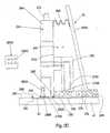
- Figure 2Ais a cut-away view taken on line 2A-2A in Figure 1 that illustrates a portion of the exposure apparatus 10 including the optical assembly 16, the device stage 42, the environmental system 26, and the wafer 30.
- the imaging field 250(Illustrated in phantom) is also illustrated in Figure 2A .
- the environmental system 26fills the imaging field 250 and the rest of the gap 246 (illustrated in Figure 2B ) with an immersion fluid 248 (illustrated in Figure 2B ).
- the term "fluid”shall mean and include a liquid and/or a gas, including any fluid vapor.
- the environmental system 26includes an immersion fluid system 252 and a fluid barrier 254.
- the immersion fluid system 252delivers and/or injects the immersion fluid 248 into the gap 246 and captures the immersion fluid 248 flowing from the gap 246, and
- the fluid barrier 254inhibits the flow of the immersion fluid 248 away from near the gap 246.
- the design of the immersion fluid system 252can vary.
- the immersion fluid system 252can inject the immersion fluid 24B at one or more locations at or near the gap 246 and/or the edge of the optical assembly 16.
- the immersion fluid 248may be injected directly between the optical assembly 16 and the wafer 30.
- the immersion fluid system 252can scavenge the immersion fluid 248 at one or more locations at or near the gap 246 and/or the edge of the optical assembly 16.
- the immersion fluid system 252includes four, spaced apart injector/scavenge pads 258 (illustrated in phantom) positioned near the perimeter of the optical assembly 16 and an injector/scavenge source 260. These components are described in more detail below.
- Figure 2Aalso illustrates that the optical assembly 16 includes an optical housing 262A, a last optical element 262B, and an element retainer 262C that secures the last optical element 262B to the optical housing 262A.
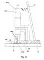
- Figure 2Bis a cut-away view of the portion of the exposure apparatus 10 of Figure 2A , including (i) the optical assembly 16 with the optical housing 262A, the optical element 262B, and the element retainer 262C, (ii) the device stage 42, and (iii) the environmental system 26.
- Figure 2Balso illustrates the gap 246 between the last optical element 262B and the wafer 30, and that the immersion fluid 248 (illustrated as circles) fills the gap 246.
- the gap 246is approximately 1mm.
- the fluid barrier 254contains the immersion fluid 248, including any fluid vapor 249 (illustrated as triangles) in the area near the gap 246 and forms and defines an interior chamber 263 around the gap 246.
- the fluid barrier 254includes a containment frame 264 (also referred to herein as a surrounding member), a seal 266, and a frame support 268.
- the interior chamber 263represents the enclosed volume defined by the containment frame 264, the seal 266, the optical housing 262A and the wafer 30.
- the fluid barrier 254restricts the flow of the immersion fluid 248 from the gap 246, assists in maintaining the gap 246 full of the immersion fluid 248, allows for the recovery of the immersion fluid 248 that escapes from the gap 246, and contains any vapor 249 from the fluid.
- the fluid barrier 254encircles and runs entirely around the gap 246. Further, in one embodiment, the fluid barrier 254 confines the immersion fluid 248 and its vapor 249 to a region on the wafer 30 and the device stage 42 centered on the optical assembly 16.
- Containment of both the immersion fluid 248 and its vapor 249can be important for the stability of the lithography tool.
- stage measurement interferometersare sensitive to the index of refraction of the ambient atmosphere. For the case of air with some water vapor present at room temperature and 633 nm laser light for the interferometer beam, a change of 1% in relative humidity causes a change in refractive index of approximately 10 -8 . For a 1 m total beam path this can represent an error of 10 nm in stage position. If the immersion fluid 248 is water, a droplet of water 7 mm in diameter evaporating into a 1 m 3 volume changes the relative humidity by 1%.
- Relative humidityis typically monitored and corrected for by the control system 24, but this is based on the assumption that the relative humidity is uniform, so that its value is the same in the interferometer beams as at the monitoring point. However, if droplets of water and its attendant vapor are scattered around on the wafer and stage surfaces, the assumption of uniform relative humidity may not be valid.
- water evaporationmay also create temperature control problems.
- the heat of vaporization of wateris about 44 kJ/mole. Evaporation of the 7 mm drop mentioned above will absorb about 430 J which must be supplied by the adjacent surfaces.
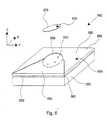
- Figure 2Cillustrates a perspective view of one embodiment of the containment frame 264.
- the containment frame 264is annular ring shaped and encircles the gap 246 (illustrated in Figure 2B ).
- the containment frame 264includes a top side 270A, an opposed bottom side 270B (also referred to as a first surface) that faces the wafer 30, an inner side 270C that faces the gap 246, and an outer side 270D.
- top and bottomare used merely for convenience and the orientation of the containment frame 264 can be rotated.
- the containment frame 264can have another shape.
- the containment frame 264can be rectangular frame shaped or octagonal frame shaped.
- the containment frame 254may be temperature controlled to stabilize the temperature of the immersion fluid 248.
- the seal 266seals the containment frame 264 to the optical assembly 16 and allows for some motion of the containment frame 264 relative to the optical assembly 16.
- the seal 266is made of a flexible, resilient material that is not influenced by the immersion fluid 248. Suitable materials for the seal 266 include rubber, Buna-N, neoprene, Viton or plastic. Alternatively the seal 266 may be a bellows made of a metal such as stainless steel or rubber or a plastic.
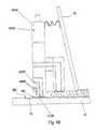
- Figure 2Dillustrates an enlarged view of a portion of Figure 2B , in partial cut-away.
- the frame support 268connects and supports the containment frame 264 to the apparatus frame 12 and the optical assembly 16 above the wafer 30 and the device stage 42.
- the frame support 268supports all of the weight of the containment frame 264.
- the frame support 268can support only a portion of the weight of the containment frame 264.
- the frame support 268can include one or more support assemblies 274.
- the frame support 268can include three spaced apart support assemblies 274 (only two are illustrated). In this embodiment, each support assembly 274 extends between the apparatus frame 12 and the top side 270A of the containment frame 264.
- each support assembly 274is a flexure.
- the term "flexure”shall mean a part that has relatively high stiffness in some directions and relatively low stiffness in other directions.
- the flexurescooperate (i) to be relatively stiff along the X axis and along the Y axis, and (ii) to be relatively flexible along the Z axis.
- the ratio of relatively stiff to relatively flexibleis at least approximately 100/1, and can be at least approximately 1000/1.
- the flexurescan allow for motion of the containment frame 264 along the Z axis and inhibit motion of the containment frame 264 along the X axis and the Y axis.
- the support assembly 274passively supports the containment frame 264.
- each support assembly 274can be an actuator that can be used to adjust the position of the containment frame 264 relative to the wafer 30 and the device stage 42.
- the frame support 268can include a frame measurement system 275 that monitors the position of the containment frame 264.
- the frame measurement system 275can monitor the position of the containment frame 264 along the Z axis, about the X axis, and/or about the Y axis. With this information, the support assemblies 274 can be used to adjust the position of the containment frame 264. In this embodiment, the support assembly 274 can actively adjust the position of the containment frame 264.
- the environmental system 26includes one or more pressure equalizers 276 that can be used to control the pressure in the chamber 263.
- the pressure equalizers 276inhibit atmospheric pressure changes or pressure changes associated with the fluid control from creating forces between the containment frame 264 and the wafer 30 or the last optical element 262B.
- the pressure equalizers 276can cause the pressure on the inside of the chamber 263 and/or in the gap 246 to be approximately equal to the pressure on the outside of the chamber 263.
- each pressure equalizer 276can be a channel that extends through the containment frame 264.
- a tube 277(only one is illustrated) is attached to the channel of each pressure equalizer 276 to convey any fluid vapor away from the measurement system 22 (illustrated in Figure 1 ).
- the pressure equalizer 276allow for a pressure difference of less than approximately 0.01, 0.05, 0.1, 0.5, or 1.0 PSI.
- FIG. 2Balso illustrates several injector/scavenge pads 258.
- Figure 2Dillustrates one injector/scavenge pad 258 in more detail.
- each of the injector/scavenge pads 258includes a pad outlet 278A and a pad inlet 278B that are in fluid communication with the injector/scavenge source 260.
- the injector/scavenge source 260provides immersion fluid 248 to the pad outlet 278A that is released into the chamber 263 and draws immersion fluid 248 through the pad inlets 278B from the chamber 263.
- Figures 2B and 2Dalso illustrate that the immersion fluid 248 in the chamber 263 sits on top of the wafer 30. As the wafer 30 moves under the optical assembly 16, it will drag the immersion fluid 248 in the vicinity of a top, device surface 279 of the wafer 30 with the wafer 30 into the gap 246.
- the device stage 42includes a stage surface 280 that has approximately the same height along the Z axis as the top, device exposed surface 279 of the wafer 30. Stated another way, in one embodiment, the stage surface 280 is in approximately the same plane as the device exposed surface 279. In alternative embodiments, for example, approximately the same plane shall mean that the planes are within approximately 1, 10, 100 or 500 microns. As a result thereof, the distance between the bottom side 270B of the containment frame 264 and the wafer 30 is approximately equal to the distance between the bottom side 270B of the containment frame 264 and the device stage 42. In one embodiment, for example, the device stage 42 can include a disk shaped recess 282 for receiving the wafer 30. Alternative designs of the device stage 42 are discussed below.
- Figure 2Dillustrates that a frame gap 284 exists between the bottom side 270B of the containment frame 264 and the wafer 30 and/or the device stage 42 to allow for ease of movement of the device stage 42 and the wafer 30 relative to the containment frame 264.
- the size of the frame gap 284can vary.
- the frame gap 284can be between approximately 5 ⁇ m and 3 mm.
- the frame gap 284can be approximately 5, 10, 50, 100, 150, 200, 250, 300, 400, or 500 microns.
- the distance between the bottom side 270B and at least one of the wafer 30 and/or the device stage 42is shorter than a distance between the end surface (e.g. the last optical element 262B or the bottom of the optical housing 262A) of the optical assembly 16 and at least one of the wafer 30 and/or the device stage 42.
- a wafer gap 285can exist between the edge of the wafer 30 and the wafer stage 42.
- the wafer gap 285is as narrow as possible to minimize leakage when the wafer 30 is off-center from the optical assembly 16 and lying partly within and partly outside the fluid containment frame 264 region.
- the wafer gap 285can be approximately 1, 10, 50, 100, 500, or 1000 microns.
- Figure 2Dalso illustrates that some of the immersion fluid 248 flows between the containment frame 264 and the wafer 30 and/or the device stage 42.
- the containment frame 264includes one or more scavenge inlets 286 that are positioned at or near the bottom side 270B of the containment frame 264.
- the one or more scavenge inlets 286are in fluid communication with the injector/scavenge source 260 (illustrated in Figure 2B ).
- the immersion fluid 248 that escapes in the frame gap 284can be scavenged by the injector/scavenge source 260.
- the bottom side 270B of the containment frame 264includes one scavenge inlet 286 that is substantially annular groove shaped and is substantially concentric with the optical assembly 16.
- the bottom side 270B of the containment frame 264can include a plurality of spaced apart annular groove shaped, scavenge inlets 286 that are substantially concentric with the optical assembly 16 to inhibit the immersion fluid 248 from completely exiting the frame gap 284.
- a plurality of spaced apart apertures oriented in a circlecan be used instead of an annular shaped groove.
- the injector/scavenge source 260applies a vacuum and/or partial vacuum on the scavenge inlet 286.
- the partial vacuumdraws the immersion fluid 248 between (i) a small land area 288 on the bottom side 270B, and (ii) the wafer 30 and/or the device stage 42.
- the immersion fluid 248 in the frame gap 284acts as a fluid bearing 289A (illustrated as an arrow) that supports the containment frame 264 above the wafer 30 and/or the device stage 42, allows for the containment frame 264 to float with minimal friction on the wafer 30 and/or the device stage 42, and allows for a relatively small frame gap 284.
- most of the immersion fluid 248is confined within the fluid barrier 254 and most of the leakage around the periphery is scavenged within the narrow frame gap 284.
- the environmental system 26can include a device for creating an additional fluid bearing 289B (illustrated as an arrow) between the containment frame 264 and the wafer 30 and/or the device stage 42.
- the containment frame 264can include one or more bearing outlets 290A that are in fluid communication with a bearing fluid source 290B of a bearing fluid 290C (illustrated as triangles).
- the bearing fluid 290Cis air.
- the bearing fluid source 290Bprovides pressurized air 290C to the bearing outlet 290A to create the aerostatic bearing 289B.
- the fluid bearings 289A, 289Bcan support all or a portion of the weight of the containment frame 264.
- one or both of the fluid bearings 289A, 289Bsupport approximately 1, 5, 10, 20, 30, 40, 50, 60, 70, 80, 90, or 100 percent of the weight of the containment frame 264.
- the concentric fluid bearings 289A, 289Bare used to maintain the frame gap 284.
- the bearing fluid 290Ccan have the same composition or a different composition than the immersion fluid 248. However, some of the bearing fluid 290C may escape from the fluid barrier 254. In one embodiment, the type of bearing fluid 290C is be chosen so that the bearing fluid 290C and its vapor do not interfere with the measurement system 22 or temperature stability of the exposure apparatus 10.
- the partial vacuum in the scavenge inlets 286pulls and urges the containment frame 264 towards the wafer 30.
- the fluid bearing 289Bsupports part of the weight of the containment frame 264 as well as opposes the pre-load imposed by the partial vacuum in the scavenge inlets 286.
- the pressurized air 290Chelps to contain the immersion fluid 248 within the containment frame 264.
- the immersion fluid 248 in the frame gap 284is mostly drawn out through the scavenge inlets 286.
- any immersion fluid 248 which leaks beyond the scavenge inlets 286is pushed back to the scavenge inlets 286 by the bearing fluid 290C.
- the frame gap 284may vary radially, from the inner side 270C to the outer side 270D, to optimize bearing and scavenging functions.
- the bearing outlet 290Ais substantially annular groove shaped, is substantially concentric with the optical assembly 16 and the scavenge inlet 286, and has a diameter that is greater than the diameter of the scavenge inlet 286.
- the bottom side 270B of the containment frame 264can include a plurality of spaced apart annular groove shaped, bearing outlets 290A that are substantially concentric with the optical assembly 16.
- a plurality of spaced apart apertures oriented in a circlecan be used instead of an annular shaped groove.
- a magnetic type bearingcould be used to support the containment frame 264.
- FIG. 2Eis an illustration of the portion of the exposure apparatus 10 of Figure 2A with the device stage 42 and the wafer 30 moved relative to the optical assembly 16. In this position, the wafer 30 and the device stage 42 are no longer centered under the optical assembly 16, and the fluid bearings 289A, 289A (illustrated in Figure 2D ) support the containment frame 264 above the wafer 30 and the device stage 42.
- Figure 3is a first embodiment of the injector/scavenge source 260.
- the injector/scavenge source 260includes (i) a low pressure source 392A, e.g. a pump, having an inlet that is at a vacuum or partial vacuum that is in fluid communication with the scavenge inlet 286 (illustrated in Figure 2D ) and the pad inlets 278B (illustrated in Figures 2B and 2D ) and a pump outlet that provides pressurized immersion fluid 248, (ii) a filter 392B in fluid communication with the pump outlet that filters the immersion fluid 248, (iii) an aerator 392C in fluid communication with the filter 392B that removes any air, contaminants, or gas from the immersion fluid 248, (iv) a temperature control 392D in fluid communication with the aerator 392C that controls the temperature of the immersion fluid 248, (v) a reservoir 392E in fluid communication with the temperature control 392D that retains the immersion fluid 248, and
- control system 24(illustrated in Figure 1 ) to control the flow rate of the immersion fluid 248 to the pad outlets 278A, the temperature of the immersion fluid 248 at the pad outlets 278A, the pressure of the immersion fluid 248 at the pad outlets 278A, and/or the pressure at the scavenge inlets 286 and the pad inlets 278B.
- the injector/scavenge source 260can include (i) a pair of pressure sensors 392G that measure the pressure near the pad outlets 278A, the scavenge inlet 286 and the pad inlets 278B, (ii) a flow sensor 392H that measures the flow to the pad outlets 278A, and/or (iii) a temperature sensor 3921 that measures the temperature of the immersion fluid 248 delivered to the pad outlets 278A.
- the information from these sensors 392G-392Ican be transferred to the control system 24 so that that control system 24 can appropriately adjust the other components of the injector/scavenge source 260 to achieve the desired temperature, flow and/or pressure of the immersion fluid 248.
- orientation of the components of the injector/scavenge source 260can be varied. Further, one or more of the components may not be necessary and/or some of the components can be duplicated.
- the injector/scavenge source 260can include multiple pumps, multiple reservoirs, temperature controllers or other components.
- the environmental system 26can include multiple injector/scavenge sources 26.
- the rate at which the immersion fluid 248 is pumped into and out of the chamber 263can be adjusted to suit the design requirements of the system. Further, the rate at which the immersion fluid 248 is scavenged from the pad inlets 278B and the scavenge inlets 286 can vary. In one embodiment, the immersion fluid 248 is scavenged from the pad inlets 278B at a first rate and is scavenged from the scavenge inlets 286 at a second rate. As an example, the first rate can be between approximately 0.1- 5 liters/minute and the second rate can be between approximately 0.01- 0.5 liters/minute. However, other first and second rates can be utilized.
- the rates at which the immersion fluid 248 is pumped into and out of the chamber 263can be adjusted to (i) control the leakage of the immersion fluid 248 below the fluid barrier, (ii) control the leakage of the immersion fluid 248 from the wafer gap 285 when the wafer 30 is off-center from the optical assembly 16, and/or (iii) control the temperature and purity of the immersion fluid 248 in the gap 246.
- the ratescan be increased in the event the wafer 30 is off-center, the temperature of the immersion fluid 248 becomes too high and/or there is an unacceptable percentage of contaminants in the immersion fluid 248 in the gap 246.
- the type of immersion fluid 248can be varied to suit the design requirements of the apparatus 10.
- the immersion fluid 248is water.
- the immersion fluid 248can be a fluorocarbon fluid, Fomblin oil, a hydrocarbon oil, or another type of oil.
- the fluidshould satisfy certain conditions: 1) it must be relatively transparent to the exposure radiation; 2) its refractive index must be comparable to that of the last optical element 262B; 3) it should not react chemically with components of the exposure system 10 with which it comes into contact; 4) it must be homogeneous; and 5) its viscosity should be low enough to avoid transmitting vibrations of a significant magnitude from the stage system to the last optical element 262B.
- Figure 4Ais an enlarged view of a portion of another embodiment of the fluid barrier 454A, a portion of the wafer 30, and a portion of the device stage 42.
- the fluid barrier 454Ais somewhat similar to the corresponding component described above and illustrated in Figure 2D .
- the containment frame 464Aincludes two concentric, scavenge inlets 486A that are positioned at the bottom side 470B of the containment frame 464A.
- the two scavenge inlets 486Aare in fluid communication with the injector/scavenge source 260 (illustrated in Figure 2B ).
- the immersion fluid 248 that escapes in the frame gap 284can be scavenged by the injector/scavenge source 260.
- the bottom side 470B of the containment frame 464includes two scavenge inlets 486A that are each substantially annular groove shaped and are substantially concentric with the optical assembly 16.
- the injector/scavenge source 260applies a vacuum or partial vacuum on the scavenge inlets 486A.
- the partial vacuumdraws the immersion fluid 248 between a small land area 488 on the bottom side 470B and the wafer 30 and/or the device stage 42.
- the majority of the immersion fluid 248flows under the land 488 and into the inner scavenge inlet 486A.
- the immersion fluid 248 not removed at the inner scavenge inlet 486Ais drawn into the outer scavenge inlet 486A.
- Figure 4Bis an enlarged view of a portion of another embodiment of the fluid barrier 454B, a portion of the wafer 30, and a portion of the device stage 42.
- the fluid barrier 454Bis somewhat similar to the corresponding component described above and illustrated in Figure 2D .
- the containment frame 464Bincludes one bearing outlet 490B and two scavenge inlets 486B that are positioned at the bottom side 470B.
- the scavenge inlets 486Bare in fluid communication with the injector/scavenge source 260 (illustrated in Figure 2B ) and the bearing outlet 490B is in fluid communication with the bearing fluid source 290C (illustrated in Figure 2D ).
- the bearing outlet 490Bis positioned within and concentric with the scavenge inlets 486B. Stated another way, the bearing outlet 490B has a smaller diameter than the scavenge inlets 486B and the bearing outlet 490B is closer to the optical assembly 16 than the scavenge inlets 486B.
- the bearing fluid 290C(illustrated in Figure 2D ) can be a liquid that is the same in composition as the immersion fluid 248. With this design, the bearing fluid 290C in the frame gap 284 can be scavenged by the injector/scavenge source 260 via the scavenge inlets 4868.
- Figure 4Cis an enlarged view of a portion of another embodiment of the fluid barrier 454C, a portion of the wafer 30, and a portion of the device stage 42.
- the fluid barrier 454Cis somewhat similar to the corresponding component described above and illustrated in Figure 2D .
- the containment frame 464Cincludes one bearing outlet 490C and two scavenge inlets 486C that are positioned at the bottom side 470B.
- the scavenge inlets 486Care in fluid communication with the injector/scavenge source 260 (illustrated in Figure 2B ) and the bearing outlet 490C is in fluid communication with the bearing fluid source 290C (illustrated in Figure 2D ).
- the bearing outlet 490Cis positioned between the two scavenge inlets 486C.
- the inner scavenge inlet 486Chas a smaller diameter than the bearing outlet 490C and the bearing outlet 490C has a smaller diameter than the outer scavenge inlet 486C.
- the inner scavenge inlet 486Cis closer to the optical assembly 16 than the bearing outlet 490C.
- Figure 5Ais a cut-away view of a portion of another embodiment of the exposure apparatus 510, including the optical assembly 516, the device stage 542, and the environmental system 526 that are similar to the corresponding components described above.
- Figure 5Aalso illustrates the wafer 30, the gap 546, and that the immersion fluid 548 fills the gap 546.
- Figure 5Billustrates an enlarged portion of the Figure 5A taken on line 5B-5B.
- the fluid barrier 554includes an inner barrier 555 in addition to the containment frame 564, the seal 566, and the frame support 568.
- the inner barrier 555is annular ring shaped, encircles the bottom of the optical assembly 516, is concentric with the optical assembly 516, and is positioned within the containment frame 564 adjacent to the seal 566.
- the inner barrier 555can serve several purposes.
- the inner barrier 555can limit the amount of immersion fluid 548 escaping to the containment frame 564, reducing the scavenging requirements at the scavenge inlets 586, and also reducing the leakage of immersion fluid 548 into the wafer gap 285 when the wafer 30 is off-center from the optical assembly 516 and lying partly within and partly outside the fluid containment frame 564 region.
- the fluid injection/scavenge pads 558can be used to recover the majority of the immersion fluid 548 from the chamber 563.
- the immersion fluid 548is maintained at or near the level of the top of the inner barrier 555, pressure surges associated with injection of the immersion fluid 548 can be reduced, because excess immersion fluid 548 overflows the top of the inner barrier 555, creating a static pressure head. Some pressure surge may remain even in this situation due to surface tension effects. These effects can be reduced by increasing the distance W shown in Fig. 5B . For example, if the immersion fluid is water, W should preferably be several mm or more. Additionally, the remaining pressure surge can be reduced or eliminated by adjusting the "wettability" of the surfaces of inner barrier 555 and optical assembly 516 in contact with the immersion fluid 548 to reduce surface tension forces.
- the inner barrier 555can maintain a significant fluid height difference with a gap of approximately 50 ⁇ m between the bottom of the inner barrier 55 and the top of the wafer 30 or the device stage 42.
- Figure 6is a perspective view of one embodiment of a device stage 642 with a wafer 630 positioned above the device stage 642.
- the device stage 642includes a device table 650, a device holder 652, a guard 654, and a guard mover assembly 656.
- the device table 650is generally rectangular plate shaped.
- the device holder 652retains the wafer 630.
- the device holder 652is a chuck or another type of clamp that is secured to the device table 650.
- the guard 654surrounds and/or encircles the wafer 630.
- the guard 654is generally rectangular plate shaped and includes a circular shaped aperture 658 for receiving the wafer 630.
- the guard 654can include a first section 660 and a second section 662.
- One or more of the sections 660, 662can be moved, removed or recessed to provide easy access for loading and removing the wafer 630.
- the guard mover assembly 656secures the guard 654 to the device table 650, and moves and positions the guard 654 relative to the device table 650, the device holder 652, and the wafer 630. With this design, the guard mover assembly 656 can move the guard 654 so that the top, stage surface 680 of the guard 654 is approximately at the same Z height as the top device exposed surface 679 of the wafer 630. Stated another way, the guard mover assembly 656 moves the guard 654 so that the device exposed surface 680 is approximately in the same plane as the device exposed surface 679. As a result thereof, the guard 654 can be moved to adjust for wafers 630 of alternative heights.
- the design of the guard mover assembly 656can be varied.
- the guard mover assembly 656can include one or more rotary motors, voice coil motors, linear motors, electromagnetic actuators, and/or some other type of force actuators.
- the guard mover assembly 656moves and positions the guard 654 along the Z axis, about the X axis and about the Y axis under the control of the control system 24 (illustrated in Figure 1 ).
- a sensor 681(illustrated as a box) can be used to measure the relative heights of the guard surface 680 and the wafer top surface 679. Information from the sensor 681 can be transferred to the control system 24 (illustrated in Figure 1 ) which uses information from the height sensor 681 to control the guard mover assembly 656.
- Figure 7Ais a perspective view of another embodiment of a device stage 742 with a wafer 730 positioned above the device stage 742.
- Figure 7Bis a cut-away view taken from Figure 7A .
- the device stage 742includes a device table 750, a device holder 752, a guard 754, and a holder mover assembly 756.
- the device table 750is generally rectangular plate shaped.
- the device holder 752retains the wafer 730.
- the guard 754is generally rectangular plate shaped and includes a circular shaped aperture 758 for the wafer 730. In this embodiment, the guard 754 is fixedly secured to the device table 750.
- the holder mover assembly 756secures the device holder 752 to the device table 750 and moves and positions the device holder 752 relative to the device table 750 and the guard 754. With this design, the holder mover assembly 756 can move the device holder 752 and the wafer 730 so that the top stage surface 780 of the guard 754 is approximately at the same Z height as the top device exposed surface 779 of the wafer 730.
- a sensor 781can be used to measure the relative heights of the top stage surface 780 and the top device exposed surface 779. The information from the sensor 781 can be transferred to the control system 24 (illustrated in Figure 1 ) which uses information from the height sensor to control the holder mover assembly 756.
- the holder mover assembly 756can include one or more rotary motors, voice coil motors, linear motors, electromagnetic actuators, and/or some other type of force actuators.
- the holder mover assembly 756moves and positions the device holder 750 and the wafer 730 along the Z axis, about the X axis and about the Y axis under the control of the control system 24 (illustrated in Figure 1 ).
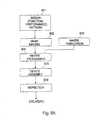
- step 801the device's function and performance characteristics are designed.
- step 802a mask (reticle) having a pattern is designed according to the previous designing step, and in a parallel step 803 a wafer is made from a silicon material.
- the mask pattern designed in step 802is exposed onto the wafer from step 803 in step 804 by a photolithography system described hereinabove in accordance with the present invention.
- step 805the semiconductor device is assembled (including the dicing process, bonding process and packaging process), finally, the device is then inspected in step 806.
- FIG 8Billustrates a detailed flowchart example of the above-mentioned step 804 in the case of fabricating semiconductor devices.
- step 811oxidation step
- step 812CVD step
- step 813electrode formation step
- step 814ion implantation step
- ionsare implanted in the wafer.
- steps 811 - 814form the preprocessing steps for wafers during wafer processing, and selection is made at each step according to processing requirements.
- step 815photoresist formation step
- step 816exposure step
- step 817developing step
- step 818etching step
- steps other than residual photoresistexposed material surface
- step 819photoresist removal step
Landscapes
- General Physics & Mathematics (AREA)
- Physics & Mathematics (AREA)
- Health & Medical Sciences (AREA)
- Engineering & Computer Science (AREA)
- Environmental & Geological Engineering (AREA)
- Public Health (AREA)
- Epidemiology (AREA)
- Atmospheric Sciences (AREA)
- Toxicology (AREA)
- Life Sciences & Earth Sciences (AREA)
- Manufacturing & Machinery (AREA)
- Computer Hardware Design (AREA)
- Microelectronics & Electronic Packaging (AREA)
- Power Engineering (AREA)
- Condensed Matter Physics & Semiconductors (AREA)
- Exposure And Positioning Against Photoresist Photosensitive Materials (AREA)
- Exposure Of Semiconductors, Excluding Electron Or Ion Beam Exposure (AREA)
Abstract
Description
- This application claims priority on Provisional Application Serial No.
60/462,112 filed on April 10, 2003 60/484,476 filed on July 1, 2003 60/462,112 60/484,476 - Lithography exposure apparatuses are commonly used to transfer images from a reticle onto a semiconductor wafer during semiconductor processing. A typical exposure apparatus includes an illumination source, a reticle stage assembly that positions a reticle, an optical assembly, a wafer stage assembly that positions a semiconductor wafer, and a measurement system that precisely monitors the position of the reticle and the wafer.
- Immersion lithography systems utilize a layer of immersion fluid that completely fills a gap between the optical assembly and the wafer. The wafer is moved rapidly in a typical lithography system and it would be expected to carry the immersion fluid away from the gap. This immersion fluid that escapes from the gap can interfere with the operation of other components of the lithography system. For example, the immersion fluid and its vapor can interfere with the measurement system that monitors the position of the wafer.
- The present invention is directed to an environmental system for controlling an environment in a gap between an optical assembly and a device that is retained by a device stage. The environmental system includes a fluid barrier and an immersion fluid system. The fluid barrier is positioned near the device and encircles the gap. The immersion fluid system delivers an immersion fluid that fills the gap.
- In one embodiment, the immersion fluid system collects the immersion fluid that is directly between the fluid barrier and at least one of the device and the device stage. In this embodiment, the fluid barrier includes a scavenge inlet that is positioned near the device, and the immersion fluid system includes a low pressure source that is in fluid communication with the scavenge inlet. Additionally, the fluid barrier can confine and contain the immersion fluid and any of the vapor from the immersion fluid in the area near the gap.
- In another embodiment, the environmental system includes a bearing fluid source that directs a bearing fluid between the fluid barrier and the device to support the fluid barrier relative to the device. In this embodiment, the fluid barrier includes a bearing outlet that is positioned near the device. Further, the bearing outlet is in fluid communication with the bearing fluid source.
- Additionally, the environmental system can include a pressure equalizer that allows the pressure in the gap to be approximately equal to the pressure outside the fluid barrier. In one embodiment, for example, the pressure equalizer is a channel that extends through the fluid barrier.
- Moreover, the device stage can include a stage surface that is in approximately the same plane as a device exposed surface of the device. As an example, the device stage can include a device holder that retains the device, a guard that defines the stage surface, and a mover assembly that moves one of the device holder and the guard so that the device exposed surface is approximately in the same plane as the stage surface. In one embodiment, the mover assembly moves the guard relative to the device and the device holder. In another embodiment, the mover assembly moves the device holder and the device relative to the guard.
- The present invention is also directed to an exposure apparatus, a wafer, a device, a method for controlling an environment in a gap, a method for making an exposure apparatus, a method for making a device, and a method for manufacturing a wafer.
Figure 1 is a side illustration of an exposure apparatus having features of the present invention;Figure 2A is a cut-away view taken online 2A-2A ofFigure 1 ;Figure 2B is a cut-away view taken online 2B-2B ofFigure 2A ;Figure 2C is a perspective view of a containment frame having features of the present invention;Figure 2D is an enlarged detailed view taken online 2D-2D inFigure 2B ;Figure 2E is an illustration of the portion of the exposure apparatus ofFigure 2A with a wafer stage moved relative to an optical assembly;Figure 3 is a side illustration of an injector/scavenge source having features of the present invention;Figure 4A is an enlarged detailed view of a portion of another embodiment of a fluid barrier;Figure 4B is an enlarged detailed view of a portion of yet another embodiment of a fluid barrier;Figure 4C is an enlarged detailed view of a portion of still another embodiment of a fluid barrier;Figure 5A is a cut-away view of a portion of another embodiment of an exposure apparatus;Figure 5B is an enlarged detailed view taken online 5B-5B inFigure 5A ;Figure 6 is a perspective view of one embodiment of a device stage having features of the present invention;Figure 7A is a perspective view of yet embodiment of a device stage having features of the present invention;Figure 7B is a cut-away view taken online 7B-7B inFigure 7A ;Figure 8A is a flow chart that outlines a process for manufacturing a device in accordance with the present invention; andFigure 8B is a flow chart that outlines device processing in more detail.Figure 1 is a schematic illustration of a precision assembly, namely anexposure apparatus 10 having features of the present invention. Theexposure apparatus 10 includes anapparatus frame 12, an illumination system 14 (irradiation apparatus), anoptical assembly 16, areticle stage assembly 18, adevice stage assembly 20, ameasurement system 22, acontrol system 24, and a fluidenvironmental system 26. The design of the components of theexposure apparatus 10 can be varied to suit the design requirements of theexposure apparatus 10.- A number of Figures include an orientation system that illustrates an X axis, a Y axis that is orthogonal to the X axis, and a Z axis that is orthogonal to the X and Y axes. It should be noted that these axes can also be referred to as the first, second and third axes.
- The
exposure apparatus 10 is particularly useful as a lithographic device that transfers a pattern (not shown) of an integrated circuit from areticle 28 onto a semiconductor wafer 30 (illustrated in phantom). Thewafer 30 is also referred to generally as a device or work piece. Theexposure apparatus 10 mounts to amounting base 32, e.g., the ground, a base, or floor or some other supporting structure. - There are a number of different types of lithographic devices. For example, the
exposure apparatus 10 can be used as a scanning type photolithography system that exposes the pattern from thereticle 28 onto thewafer 30 with thereticle 28 and thewafer 30 moving synchronously. In a scanning type lithographic device, thereticle 28 is moved perpendicularly to an optical axis of theoptical assembly 16 by thereticle stage assembly 18 and thewafer 30 is moved perpendicularly to the optical axis of theoptical assembly 16 by thewafer stage assembly 20. Scanning of thereticle 28 and thewafer 30 occurs while thereticle 28 and thewafer 30 are moving synchronously. - Alternatively, the
exposure apparatus 10 can be a step-and-repeat type photolithography system that exposes thereticle 28 while thereticle 28 and thewafer 30 are stationary. In the step and repeat process, thewafer 30 is in a constant position relative to thereticle 28 and theoptical assembly 16 during the exposure of an individual field. Subsequently, between consecutive exposure steps, thewafer 30 is consecutively moved with thewafer stage assembly 20 perpendicularly to the optical axis of theoptical assembly 16 so that the next field of thewafer 30 is brought into position relative to theoptical assembly 16 and thereticle 28 for exposure. Following this process, the images on thereticle 28 are sequentially exposed onto the fields of thewafer 30, and then the next field of thewafer 30 is brought into position relative to theoptical assembly 16 and thereticle 28. - However, the use of the
exposure apparatus 10 provided herein is not limited to a photolithography system for semiconductor manufacturing. Theexposure apparatus 10, for example, can be used as an LCD photolithography system that exposes a liquid crystal display device pattern onto a rectangular glass plate or a photolithography system for manufacturing a thin film magnetic head. - The
apparatus frame 12 supports the components of theexposure apparatus 10. Theapparatus frame 12 illustrated inFigure 1 supports thereticle stage assembly 18, thewafer stage assembly 20, theoptical assembly 16 and theillumination system 14 above the mountingbase 32. - The
illumination system 14 includes anillumination source 34 and an illuminationoptical assembly 36. Theillumination source 34 emits a beam (irradiation) of light energy. The illuminationoptical assembly 36 guides the beam of light energy from theillumination source 34 to theoptical assembly 16. The beam illuminates selectively different portions of thereticle 28 and exposes thewafer 30. InFigure 1 , theillumination source 34 is illustrated as being supported above thereticle stage assembly 18. Typically, however, theillumination source 34 is secured to one of the sides of theapparatus frame 12 and the energy beam from theillumination source 34 is directed to above thereticle stage assembly 18 with the illuminationoptical assembly 36. - The
illumination source 34 can be a light source such as a mercury g-line source (436 nm) or i-line source (365 nm), a KrF excimer laser (248 nm), an ArF excimer laser (193 nm) or a F2 laser (157 nm). Theoptical assembly 16 projects and/or focuses the light passing through thereticle 28 to thewafer 30. Depending upon the design of theexposure apparatus 10, theoptical assembly 16 can magnify or reduce the image illuminated on thereticle 28. It could also be a 1x magnification system. - When far ultra-violet radiation such as from the excimer laser is used, glass materials such as quartz and fluorite that transmit far ultra-violet rays can be used in the
optical assembly 16. Theoptical assembly 16 can be either catadioptric or refractive. - Also, with an exposure device that employs radiation of wavelength 200 nm or lower, use of the catadioptric type optical system can be considered. Examples of the catadioptric type of optical system include the disclosure Japan Patent Application Disclosure No.
8-171054 U.S. Patent No, 5,668,672 , as well as Japan Patent Application Disclosure No.10-20195 U.S. Patent No. 5,835,275 . In these cases, the reflecting optical device can be a catadioptric optical system incorporating a beam splitter and concave mirror. Japan Patent Application Disclosure No.8-334695 published in the Official Gazette for Laid-Open Patent Applications and its counterpartU.S. Patent No. 5,689,377 as well as Japan Patent Application Disclosure No.10-3039 and its counterpartU.S. Patent Application No. 873,605 (Application Date: 6-12-97) also use a reflecting-refracting type of optical system incorporating a concave mirror, etc., but without a beam splitter, and can also be employed with this invention. As far as is permitted, the disclosures in the above-mentioned U.S. patents, as well as the Japan patent applications published in the Official Gazette for Laid-Open Patent Applications are incorporated herein by reference. - In one embodiment, the
optical assembly 16 is secured to theapparatus frame 12 with one or moreoptical mount isolators 37. Theoptical mount isolators 37 inhibit vibration of theapparatus frame 12 from causing vibration to theoptical assembly 16. Eachoptical mount isolator 37 can include a pneumatic cylinder (not shown) that isolates vibration and an actuator (not shown) that isolates vibration and controls the position with at least two degrees of motion. Suitableoptical mount isolators 37 are sold by Integrated Dynamics Engineering, located in Wobum, MA. For ease of illustration, two spaced apartoptical mount isolators 37 are shown as being used to secure theoptical assembly 16 to theapparatus frame 12. However, for example, three spaced apartoptical mount isolators 37 can be used to kinematically secure theoptical assembly 16 to theapparatus frame 12. - The
reticle stage assembly 18 holds and positions thereticle 28 relative to theoptical assembly 16 and thewafer 30. In one embodiment, thereticle stage assembly 18 includes areticle stage 38 that retains thereticle 28 and a reticlestage mover assembly 40 that moves and positions thereticle stage 38 andreticle 28. - Somewhat similarly, the
device stage assembly 20 holds and positions thewafer 30 with respect to the projected image of the illuminated portions of thereticle 28. In one embodiment, thedevice stage assembly 20 includes adevice stage 42 that retains thewafer 30, adevice stage base 43 that supports and guides thedevice stage 42, and a devicestage mover assembly 44 that moves and positions thedevice stage 42 and thewafer 28 relative to theoptical assembly 16 and thedevice stage base 43. Thedevice stage 42 is described in more detail below. - Each
stage mover assembly respective stage stage mover assembly respective stage stage mover assembly 40 and the devicestage mover assembly 44 can each include one or more movers, such as rotary motors, voice coil motors, linear motors utilizing a Lorentz force to generate drive force, electromagnetic movers, planar motors, or some other force movers. - Alternatively, one of the stages could be driven by a planar motor, which drives the stage by an electromagnetic force generated by a magnet unit having two-dimensionally arranged magnets and an armature coil unit having two-dimensionally arranged coils in facing positions. With this type of driving system, either the magnet unit or the armature coil unit is connected to the stage base and the other unit is mounted on the moving plane side of the stage.
- Movement of the stages as described above generates reaction forces that can affect performance of the photolithography system. Reaction forces generated by the wafer (substrate) stage motion can be mechanically transferred to the floor (ground) by use of a frame member as described in
US Patent No. 5,528,100 and published Japanese Patent Application Disclosure No.8-136475 . Additionally, reaction forces generated by the reticle (mask) stage motion can be mechanically transferred to the floor (ground) by use of a frame member as described inUS Patent No. 5,874,820 and published Japanese Patent Application Disclosure No.8-330224 . As far as is permitted, the disclosures inUS Patent Numbers 5,528,100 and5,874,820 and Japanese Patent Application Disclosure No.8-330224 are incorporated herein by reference. - The
measurement system 22 monitors movement of thereticle 28 and thewafer 30 relative to theoptical assembly 16 or some other reference. With this information, thecontrol system 24 can control thereticle stage assembly 18 to precisely position thereticle 28 and thedevice stage assembly 20 to precisely position thewafer 30. The design of themeasurement system 22 can vary. For example, themeasurement system 22 can utilize multiple laser interferometers, encoders, mirrors, and/or other measuring device. The stability of themeasurement system 22 is essential for accurate transfer of an image from thereticle 28 to thewafer 30. - The
control system 24 receives information from themeasurement system 22 and controls thestage mover assemblies reticle 28 and thewafer 30. Additionally, thecontrol system 24 can control the operation of theenvironmental system 26. Thecontrol system 24 can include one or more processors and circuits. - The
environmental system 26 controls the environment in a gap 246 (illustrated inFigure 2B ) between theoptical assembly 16 and thewafer 30. Thegap 246 includes an imaging field 250 (illustrated inFigure 2A ). Theimaging field 250 includes the area adjacent to the region of thewafer 30 that is being exposed and the area in which the beam of light energy travels between theoptical assembly 16 and thewafer 30. With this design, theenvironment system 26 can control the environment in theexposure area 250. - The desired environment created and/or controlled in the
gap 246 by theenvironmental system 26 can vary accordingly to thewafer 30 and the design of the rest of the components of theexposure apparatus 10, including theillumination system 14. For example, the desired controlled environment can be a fluid such as water. Theenvironmental system 26 is described in more detail below. - A photolithography system (an exposure apparatus) according to the embodiments described herein can be built by assembling various subsystems, including each element listed in the appended claims, in such a manner that prescribed mechanical accuracy, electrical accuracy, and optical accuracy are maintained. In order to maintain the various accuracies, prior to and following assembly, every optical system is adjusted to achieve its optical accuracy. Similarly, every mechanical system and every electrical system are adjusted to achieve their respective mechanical and electrical accuracies. The process of assembling each subsystem into a photolithography system includes mechanical interfaces, electrical circuit wiring connections and air pressure plumbing connections between each subsystem. Needless to say, there is also a process where each subsystem is assembled prior to assembling a photolithography system from the various subsystems. Once a photolithography system is assembled using the various subsystems, a total adjustment is performed to make sure that accuracy is maintained in the complete photolithography system. Additionally, it is desirable to manufacture an exposure system in a clean room where the temperature and cleanliness are controlled.
Figure 2A is a cut-away view taken online 2A-2A inFigure 1 that illustrates a portion of theexposure apparatus 10 including theoptical assembly 16, thedevice stage 42, theenvironmental system 26, and thewafer 30. The imaging field 250 (Illustrated in phantom) is also illustrated inFigure 2A .- In one embodiment, the
environmental system 26 fills theimaging field 250 and the rest of the gap 246 (illustrated inFigure 2B ) with an immersion fluid 248 (illustrated inFigure 2B ). As used herein, the term "fluid" shall mean and include a liquid and/or a gas, including any fluid vapor. - The design of the
environmental system 26 and the components of theenvironmental system 26 can be varied. In the embodiment illustrated inFigure 2A , theenvironmental system 26 includes animmersion fluid system 252 and afluid barrier 254. In this embodiment, (i) theimmersion fluid system 252 delivers and/or injects theimmersion fluid 248 into thegap 246 and captures theimmersion fluid 248 flowing from thegap 246, and (ii) thefluid barrier 254 inhibits the flow of theimmersion fluid 248 away from near thegap 246. - The design of the
immersion fluid system 252 can vary. For example, theimmersion fluid system 252 can inject the immersion fluid 24B at one or more locations at or near thegap 246 and/or the edge of theoptical assembly 16. Alternatively, theimmersion fluid 248 may be injected directly between theoptical assembly 16 and thewafer 30. Further, theimmersion fluid system 252 can scavenge theimmersion fluid 248 at one or more locations at or near thegap 246 and/or the edge of theoptical assembly 16. In the embodiment illustrated inFigure 2A , theimmersion fluid system 252 includes four, spaced apart injector/scavenge pads 258 (illustrated in phantom) positioned near the perimeter of theoptical assembly 16 and an injector/scavengesource 260. These components are described in more detail below. Figure 2A also illustrates that theoptical assembly 16 includes anoptical housing 262A, a lastoptical element 262B, and anelement retainer 262C that secures the lastoptical element 262B to theoptical housing 262A.Figure 2B is a cut-away view of the portion of theexposure apparatus 10 ofFigure 2A , including (i) theoptical assembly 16 with theoptical housing 262A, theoptical element 262B, and theelement retainer 262C, (ii) thedevice stage 42, and (iii) theenvironmental system 26.Figure 2B also illustrates thegap 246 between the lastoptical element 262B and thewafer 30, and that the immersion fluid 248 (illustrated as circles) fills thegap 246. In one embodiment, thegap 246 is approximately 1mm.- In one embodiment, the
fluid barrier 254 contains theimmersion fluid 248, including any fluid vapor 249 (illustrated as triangles) in the area near thegap 246 and forms and defines aninterior chamber 263 around thegap 246. In the embodiment illustrated inFigure 2B , thefluid barrier 254 includes a containment frame 264 (also referred to herein as a surrounding member), aseal 266, and aframe support 268. Theinterior chamber 263 represents the enclosed volume defined by thecontainment frame 264, theseal 266, theoptical housing 262A and thewafer 30. Thefluid barrier 254 restricts the flow of theimmersion fluid 248 from thegap 246, assists in maintaining thegap 246 full of theimmersion fluid 248, allows for the recovery of theimmersion fluid 248 that escapes from thegap 246, and contains anyvapor 249 from the fluid. In one embodiment, thefluid barrier 254 encircles and runs entirely around thegap 246. Further, in one embodiment, thefluid barrier 254 confines theimmersion fluid 248 and itsvapor 249 to a region on thewafer 30 and thedevice stage 42 centered on theoptical assembly 16. - Containment of both the
immersion fluid 248 and itsvapor 249 can be important for the stability of the lithography tool. For example, stage measurement interferometers are sensitive to the index of refraction of the ambient atmosphere. For the case of air with some water vapor present at room temperature and 633 nm laser light for the interferometer beam, a change of 1% in relative humidity causes a change in refractive index of approximately 10-8. For a 1 m total beam path this can represent an error of 10 nm in stage position. If theimmersion fluid 248 is water, a droplet ofwater 7 mm in diameter evaporating into a 1 m3 volume changes the relative humidity by 1%. Relative humidity is typically monitored and corrected for by thecontrol system 24, but this is based on the assumption that the relative humidity is uniform, so that its value is the same in the interferometer beams as at the monitoring point. However, if droplets of water and its attendant vapor are scattered around on the wafer and stage surfaces, the assumption of uniform relative humidity may not be valid. - In addition to the risk to the interferometer beams, water evaporation may also create temperature control problems. The heat of vaporization of water is about 44 kJ/mole. Evaporation of the 7 mm drop mentioned above will absorb about 430 J which must be supplied by the adjacent surfaces.
Figure 2C illustrates a perspective view of one embodiment of thecontainment frame 264. In this embodiment, thecontainment frame 264 is annular ring shaped and encircles the gap 246 (illustrated inFigure 2B ). Additionally, in this embodiment, thecontainment frame 264 includes atop side 270A, an opposedbottom side 270B (also referred to as a first surface) that faces thewafer 30, aninner side 270C that faces thegap 246, and anouter side 270D. It should be noted that the terms top and bottom are used merely for convenience and the orientation of thecontainment frame 264 can be rotated. It should also be noted that thecontainment frame 264 can have another shape. Alternatively, for example, thecontainment frame 264 can be rectangular frame shaped or octagonal frame shaped.- Additionally, as provided herein, the
containment frame 254 may be temperature controlled to stabilize the temperature of theimmersion fluid 248. - Referring back to
Figure 2B , theseal 266 seals thecontainment frame 264 to theoptical assembly 16 and allows for some motion of thecontainment frame 264 relative to theoptical assembly 16. In one embodiment, theseal 266 is made of a flexible, resilient material that is not influenced by theimmersion fluid 248. Suitable materials for theseal 266 include rubber, Buna-N, neoprene, Viton or plastic. Alternatively theseal 266 may be a bellows made of a metal such as stainless steel or rubber or a plastic. Figure 2D illustrates an enlarged view of a portion ofFigure 2B , in partial cut-away. Theframe support 268 connects and supports thecontainment frame 264 to theapparatus frame 12 and theoptical assembly 16 above thewafer 30 and thedevice stage 42. In one embodiment, theframe support 268 supports all of the weight of thecontainment frame 264. Alternatively, for example, theframe support 268 can support only a portion of the weight of thecontainment frame 264. In one embodiment, theframe support 268 can include one ormore support assemblies 274. For example, theframe support 268 can include three spaced apart support assemblies 274 (only two are illustrated). In this embodiment, eachsupport assembly 274 extends between theapparatus frame 12 and thetop side 270A of thecontainment frame 264.- In one embodiment, each
support assembly 274 is a flexure. As used herein, the term "flexure" shall mean a part that has relatively high stiffness in some directions and relatively low stiffness in other directions. In one embodiment, the flexures cooperate (i) to be relatively stiff along the X axis and along the Y axis, and (ii) to be relatively flexible along the Z axis. The ratio of relatively stiff to relatively flexible is at least approximately 100/1, and can be at least approximately 1000/1. Stated another way, the flexures can allow for motion of thecontainment frame 264 along the Z axis and inhibit motion of thecontainment frame 264 along the X axis and the Y axis. In this embodiment, thesupport assembly 274 passively supports thecontainment frame 264. - Alternatively, for example, each
support assembly 274 can be an actuator that can be used to adjust the position of thecontainment frame 264 relative to thewafer 30 and thedevice stage 42. Additionally, theframe support 268 can include aframe measurement system 275 that monitors the position of thecontainment frame 264. For example, theframe measurement system 275 can monitor the position of thecontainment frame 264 along the Z axis, about the X axis, and/or about the Y axis. With this information, thesupport assemblies 274 can be used to adjust the position of thecontainment frame 264. In this embodiment, thesupport assembly 274 can actively adjust the position of thecontainment frame 264. - In one embodiment, the
environmental system 26 includes one ormore pressure equalizers 276 that can be used to control the pressure in thechamber 263. Stated another way, thepressure equalizers 276 inhibit atmospheric pressure changes or pressure changes associated with the fluid control from creating forces between thecontainment frame 264 and thewafer 30 or the lastoptical element 262B. For example, thepressure equalizers 276 can cause the pressure on the inside of thechamber 263 and/or in thegap 246 to be approximately equal to the pressure on the outside of thechamber 263. For example, eachpressure equalizer 276 can be a channel that extends through thecontainment frame 264. In one embodiment, a tube 277 (only one is illustrated) is attached to the channel of eachpressure equalizer 276 to convey any fluid vapor away from the measurement system 22 (illustrated inFigure 1 ). In alternative embodiments, thepressure equalizer 276 allow for a pressure difference of less than approximately 0.01, 0.05, 0.1, 0.5, or 1.0 PSI. Figure 2B also illustrates several injector/scavenge pads 258.Figure 2D illustrates one injector/scavenge pad 258 in more detail. In this embodiment, each of the injector/scavenge pads 258 includes apad outlet 278A and apad inlet 278B that are in fluid communication with the injector/scavengesource 260. At the appropriate time, the injector/scavengesource 260 providesimmersion fluid 248 to thepad outlet 278A that is released into thechamber 263 and drawsimmersion fluid 248 through thepad inlets 278B from thechamber 263.Figures 2B and2D also illustrate that theimmersion fluid 248 in thechamber 263 sits on top of thewafer 30. As thewafer 30 moves under theoptical assembly 16, it will drag theimmersion fluid 248 in the vicinity of a top,device surface 279 of thewafer 30 with thewafer 30 into thegap 246.- In one embodiment, referring to
Figures 2B and2D , thedevice stage 42 includes astage surface 280 that has approximately the same height along the Z axis as the top, device exposedsurface 279 of thewafer 30. Stated another way, in one embodiment, thestage surface 280 is in approximately the same plane as the device exposedsurface 279. In alternative embodiments, for example, approximately the same plane shall mean that the planes are within approximately 1, 10, 100 or 500 microns. As a result thereof, the distance between thebottom side 270B of thecontainment frame 264 and thewafer 30 is approximately equal to the distance between thebottom side 270B of thecontainment frame 264 and thedevice stage 42. In one embodiment, for example, thedevice stage 42 can include a disk shapedrecess 282 for receiving thewafer 30. Alternative designs of thedevice stage 42 are discussed below. Figure 2D illustrates that aframe gap 284 exists between thebottom side 270B of thecontainment frame 264 and thewafer 30 and/or thedevice stage 42 to allow for ease of movement of thedevice stage 42 and thewafer 30 relative to thecontainment frame 264. The size of theframe gap 284 can vary. For example, theframe gap 284 can be between approximately 5µm and 3 mm. In alternative examples, theframe gap 284 can be approximately 5, 10, 50, 100, 150, 200, 250, 300, 400, or 500 microns.- In certain embodiments, the distance between the
bottom side 270B and at least one of thewafer 30 and/or thedevice stage 42 is shorter than a distance between the end surface (e.g. the lastoptical element 262B or the bottom of theoptical housing 262A) of theoptical assembly 16 and at least one of thewafer 30 and/or thedevice stage 42. - Additionally, a
wafer gap 285 can exist between the edge of thewafer 30 and thewafer stage 42. In one embodiment, thewafer gap 285 is as narrow as possible to minimize leakage when thewafer 30 is off-center from theoptical assembly 16 and lying partly within and partly outside thefluid containment frame 264 region. For example, in alternative embodiments, thewafer gap 285 can be approximately 1, 10, 50, 100, 500, or 1000 microns. Figure 2D also illustrates that some of theimmersion fluid 248 flows between thecontainment frame 264 and thewafer 30 and/or thedevice stage 42. in one embodiment, thecontainment frame 264 includes one or morescavenge inlets 286 that are positioned at or near thebottom side 270B of thecontainment frame 264. The one or morescavenge inlets 286 are in fluid communication with the injector/scavenge source 260 (illustrated inFigure 2B ). With this design, theimmersion fluid 248 that escapes in theframe gap 284 can be scavenged by the injector/scavengesource 260. In the embodiment illustrated inFigure 2D , thebottom side 270B of thecontainment frame 264 includes onescavenge inlet 286 that is substantially annular groove shaped and is substantially concentric with theoptical assembly 16. Alternatively, for example, thebottom side 270B of thecontainment frame 264 can include a plurality of spaced apart annular groove shaped, scavengeinlets 286 that are substantially concentric with theoptical assembly 16 to inhibit theimmersion fluid 248 from completely exiting theframe gap 284. Still alternatively, a plurality of spaced apart apertures oriented in a circle can be used instead of an annular shaped groove.- In one embodiment, the injector/scavenge
source 260 applies a vacuum and/or partial vacuum on thescavenge inlet 286. The partial vacuum draws theimmersion fluid 248 between (i) asmall land area 288 on thebottom side 270B, and (ii) thewafer 30 and/or thedevice stage 42. Theimmersion fluid 248 in theframe gap 284 acts as a fluid bearing 289A (illustrated as an arrow) that supports thecontainment frame 264 above thewafer 30 and/or thedevice stage 42, allows for thecontainment frame 264 to float with minimal friction on thewafer 30 and/or thedevice stage 42, and allows for a relativelysmall frame gap 284. With this embodiment, most of theimmersion fluid 248 is confined within thefluid barrier 254 and most of the leakage around the periphery is scavenged within thenarrow frame gap 284. - Additionally, the
environmental system 26 can include a device for creating an additional fluid bearing 289B (illustrated as an arrow) between thecontainment frame 264 and thewafer 30 and/or thedevice stage 42. For example, thecontainment frame 264 can include one ormore bearing outlets 290A that are in fluid communication with a bearingfluid source 290B of a bearingfluid 290C (illustrated as triangles). In one embodiment, the bearing fluid 290C is air. In this embodiment, the bearingfluid source 290B providespressurized air 290C to thebearing outlet 290A to create theaerostatic bearing 289B. Thefluid bearings containment frame 264. In alternative embodiments, one or both of thefluid bearings containment frame 264. In one embodiment, theconcentric fluid bearings frame gap 284. - Depending upon the design, the bearing
fluid 290C can have the same composition or a different composition than theimmersion fluid 248. However, some of the bearing fluid 290C may escape from thefluid barrier 254. In one embodiment, the type of bearing fluid 290C is be chosen so that the bearing fluid 290C and its vapor do not interfere with themeasurement system 22 or temperature stability of theexposure apparatus 10. - In another embodiment, the partial vacuum in the
scavenge inlets 286 pulls and urges thecontainment frame 264 towards thewafer 30. in this embodiment, thefluid bearing 289B supports part of the weight of thecontainment frame 264 as well as opposes the pre-load imposed by the partial vacuum in thescavenge inlets 286. - In addition, the
pressurized air 290C helps to contain theimmersion fluid 248 within thecontainment frame 264. As provided above, theimmersion fluid 248 in theframe gap 284 is mostly drawn out through thescavenge inlets 286. In this embodiment, anyimmersion fluid 248 which leaks beyond thescavenge inlets 286 is pushed back to thescavenge inlets 286 by the bearing fluid 290C. - The
frame gap 284 may vary radially, from theinner side 270C to theouter side 270D, to optimize bearing and scavenging functions. - In
Figure 2D , thebearing outlet 290A is substantially annular groove shaped, is substantially concentric with theoptical assembly 16 and thescavenge inlet 286, and has a diameter that is greater than the diameter of thescavenge inlet 286. Alternatively, for example, thebottom side 270B of thecontainment frame 264 can include a plurality of spaced apart annular groove shaped, bearingoutlets 290A that are substantially concentric with theoptical assembly 16. Still alternatively, a plurality of spaced apart apertures oriented in a circle can be used instead of an annular shaped groove. Alternatively, for example, a magnetic type bearing could be used to support thecontainment frame 264. - As illustrated in
Figures 2B and2D , thewafer 30 is centered under theoptical assembly 16. In this position, thefluid bearings containment frame 264 above thewafer 30.Figure 2E is an illustration of the portion of theexposure apparatus 10 ofFigure 2A with thedevice stage 42 and thewafer 30 moved relative to theoptical assembly 16. In this position, thewafer 30 and thedevice stage 42 are no longer centered under theoptical assembly 16, and thefluid bearings Figure 2D ) support thecontainment frame 264 above thewafer 30 and thedevice stage 42. Figure 3 is a first embodiment of the injector/scavengesource 260. In this embodiment, the injector/scavengesource 260 includes (i) alow pressure source 392A, e.g. a pump, having an inlet that is at a vacuum or partial vacuum that is in fluid communication with the scavenge inlet 286 (illustrated inFigure 2D ) and thepad inlets 278B (illustrated inFigures 2B and2D ) and a pump outlet that providespressurized immersion fluid 248, (ii) afilter 392B in fluid communication with the pump outlet that filters theimmersion fluid 248, (iii) an aerator 392C in fluid communication with thefilter 392B that removes any air, contaminants, or gas from theimmersion fluid 248, (iv) atemperature control 392D in fluid communication with the aerator 392C that controls the temperature of theimmersion fluid 248, (v) areservoir 392E in fluid communication with thetemperature control 392D that retains theimmersion fluid 248, and (vi) aflow controller 392F that has an inlet in fluid communication with thereservoir 392E and an outlet in fluid communication with thepad outlets 278A (illustrated inFigures 2B and2D ), theflow controller 392F controlling the pressure and flow to thepad outlets 278A. The operation of these components can be controlled by the control system 24 (illustrated inFigure 1 ) to control the flow rate of theimmersion fluid 248 to thepad outlets 278A, the temperature of theimmersion fluid 248 at thepad outlets 278A, the pressure of theimmersion fluid 248 at thepad outlets 278A, and/or the pressure at thescavenge inlets 286 and thepad inlets 278B.- Additionally, the injector/scavenge
source 260 can include (i) a pair ofpressure sensors 392G that measure the pressure near thepad outlets 278A, thescavenge inlet 286 and thepad inlets 278B, (ii) aflow sensor 392H that measures the flow to thepad outlets 278A, and/or (iii) atemperature sensor 3921 that measures the temperature of theimmersion fluid 248 delivered to thepad outlets 278A. The information from thesesensors 392G-392I can be transferred to thecontrol system 24 so that thatcontrol system 24 can appropriately adjust the other components of the injector/scavengesource 260 to achieve the desired temperature, flow and/or pressure of theimmersion fluid 248. - It should be noted that orientation of the components of the injector/scavenge
source 260 can be varied. Further, one or more of the components may not be necessary and/or some of the components can be duplicated. For example, the injector/scavengesource 260 can include multiple pumps, multiple reservoirs, temperature controllers or other components. Moreover, theenvironmental system 26 can include multiple injector/scavenge sources 26. - The rate at which the
immersion fluid 248 is pumped into and out of the chamber 263 (illustrated inFigure 2B ) can be adjusted to suit the design requirements of the system. Further, the rate at which theimmersion fluid 248 is scavenged from thepad inlets 278B and thescavenge inlets 286 can vary. In one embodiment, theimmersion fluid 248 is scavenged from thepad inlets 278B at a first rate and is scavenged from thescavenge inlets 286 at a second rate. As an example, the first rate can be between approximately 0.1- 5 liters/minute and the second rate can be between approximately 0.01- 0.5 liters/minute. However, other first and second rates can be utilized. - It should be noted that the rates at which the
immersion fluid 248 is pumped into and out of thechamber 263 can be adjusted to (i) control the leakage of theimmersion fluid 248 below the fluid barrier, (ii) control the leakage of theimmersion fluid 248 from thewafer gap 285 when thewafer 30 is off-center from theoptical assembly 16, and/or (iii) control the temperature and purity of theimmersion fluid 248 in thegap 246. For example, the rates can be increased in the event thewafer 30 is off-center, the temperature of theimmersion fluid 248 becomes too high and/or there is an unacceptable percentage of contaminants in theimmersion fluid 248 in thegap 246. - The type of
immersion fluid 248 can be varied to suit the design requirements of theapparatus 10. In one embodiment, theimmersion fluid 248 is water. Alternatively, for example, theimmersion fluid 248 can be a fluorocarbon fluid, Fomblin oil, a hydrocarbon oil, or another type of oil. More generally, the fluid should satisfy certain conditions: 1) it must be relatively transparent to the exposure radiation; 2) its refractive index must be comparable to that of the lastoptical element 262B; 3) it should not react chemically with components of theexposure system 10 with which it comes into contact; 4) it must be homogeneous; and 5) its viscosity should be low enough to avoid transmitting vibrations of a significant magnitude from the stage system to the lastoptical element 262B. Figure 4A is an enlarged view of a portion of another embodiment of thefluid barrier 454A, a portion of thewafer 30, and a portion of thedevice stage 42. In this embodiment, thefluid barrier 454A is somewhat similar to the corresponding component described above and illustrated inFigure 2D . However, in this embodiment, thecontainment frame 464A includes two concentric, scavengeinlets 486A that are positioned at thebottom side 470B of thecontainment frame 464A. The twoscavenge inlets 486A are in fluid communication with the injector/scavenge source 260 (illustrated inFigure 2B ). With this design, theimmersion fluid 248 that escapes in theframe gap 284 can be scavenged by the injector/scavengesource 260. In this embodiment, thebottom side 470B of the containment frame 464 includes twoscavenge inlets 486A that are each substantially annular groove shaped and are substantially concentric with theoptical assembly 16.- With this design, the injector/scavenge
source 260 applies a vacuum or partial vacuum on thescavenge inlets 486A. The partial vacuum draws theimmersion fluid 248 between asmall land area 488 on thebottom side 470B and thewafer 30 and/or thedevice stage 42. In this embodiment, the majority of theimmersion fluid 248 flows under theland 488 and into theinner scavenge inlet 486A. Additionally, theimmersion fluid 248 not removed at theinner scavenge inlet 486A is drawn into theouter scavenge inlet 486A. Figure 4B is an enlarged view of a portion of another embodiment of thefluid barrier 454B, a portion of thewafer 30, and a portion of thedevice stage 42. In this embodiment, thefluid barrier 454B is somewhat similar to the corresponding component described above and illustrated inFigure 2D . However, in this embodiment, thecontainment frame 464B includes onebearing outlet 490B and twoscavenge inlets 486B that are positioned at thebottom side 470B. Thescavenge inlets 486B are in fluid communication with the injector/scavenge source 260 (illustrated inFigure 2B ) and thebearing outlet 490B is in fluid communication with the bearingfluid source 290C (illustrated inFigure 2D ). However, in this embodiment, thebearing outlet 490B is positioned within and concentric with thescavenge inlets 486B. Stated another way, thebearing outlet 490B has a smaller diameter than thescavenge inlets 486B and thebearing outlet 490B is closer to theoptical assembly 16 than thescavenge inlets 486B. Further, with this design, the bearingfluid 290C (illustrated inFigure 2D ) can be a liquid that is the same in composition as theimmersion fluid 248. With this design, the bearing fluid 290C in theframe gap 284 can be scavenged by the injector/scavengesource 260 via the scavenge inlets 4868.Figure 4C is an enlarged view of a portion of another embodiment of thefluid barrier 454C, a portion of thewafer 30, and a portion of thedevice stage 42. In this embodiment, thefluid barrier 454C is somewhat similar to the corresponding component described above and illustrated inFigure 2D . However, in this embodiment, thecontainment frame 464C includes onebearing outlet 490C and twoscavenge inlets 486C that are positioned at thebottom side 470B. Thescavenge inlets 486C are in fluid communication with the injector/scavenge source 260 (illustrated inFigure 2B ) and thebearing outlet 490C is in fluid communication with the bearingfluid source 290C (illustrated inFigure 2D ). However, in this embodiment, thebearing outlet 490C is positioned between the twoscavenge inlets 486C. Stated another way, theinner scavenge inlet 486C has a smaller diameter than thebearing outlet 490C and thebearing outlet 490C has a smaller diameter than theouter scavenge inlet 486C. With this design, theinner scavenge inlet 486C is closer to theoptical assembly 16 than thebearing outlet 490C.- It should be noted that in each embodiment, additional scavenge inlets and addition bearing outlets can be added as necessary.
Figure 5A is a cut-away view of a portion of another embodiment of theexposure apparatus 510, including theoptical assembly 516, thedevice stage 542, and theenvironmental system 526 that are similar to the corresponding components described above.Figure 5A also illustrates thewafer 30, thegap 546, and that theimmersion fluid 548 fills thegap 546.Figure 5B illustrates an enlarged portion of theFigure 5A taken online 5B-5B.- However, in the embodiment illustrated in
Figures 5A and5B , thefluid barrier 554 includes aninner barrier 555 in addition to thecontainment frame 564, theseal 566, and theframe support 568. In this embodiment, theinner barrier 555 is annular ring shaped, encircles the bottom of theoptical assembly 516, is concentric with theoptical assembly 516, and is positioned within thecontainment frame 564 adjacent to theseal 566. - The
inner barrier 555 can serve several purposes. For example, theinner barrier 555 can limit the amount ofimmersion fluid 548 escaping to thecontainment frame 564, reducing the scavenging requirements at thescavenge inlets 586, and also reducing the leakage ofimmersion fluid 548 into thewafer gap 285 when thewafer 30 is off-center from theoptical assembly 516 and lying partly within and partly outside thefluid containment frame 564 region. With this design, the fluid injection/scavenge pads 558 can be used to recover the majority of theimmersion fluid 548 from thechamber 563. Additionally, if theimmersion fluid 548 is maintained at or near the level of the top of theinner barrier 555, pressure surges associated with injection of theimmersion fluid 548 can be reduced, becauseexcess immersion fluid 548 overflows the top of theinner barrier 555, creating a static pressure head. Some pressure surge may remain even in this situation due to surface tension effects. These effects can be reduced by increasing the distance W shown inFig. 5B . For example, if the immersion fluid is water, W should preferably be several mm or more. Additionally, the remaining pressure surge can be reduced or eliminated by adjusting the "wettability" of the surfaces ofinner barrier 555 andoptical assembly 516 in contact with theimmersion fluid 548 to reduce surface tension forces. In one embodiment, theinner barrier 555 can maintain a significant fluid height difference with a gap of approximately 50 µm between the bottom of the inner barrier 55 and the top of thewafer 30 or thedevice stage 42. Figure 6 is a perspective view of one embodiment of adevice stage 642 with awafer 630 positioned above thedevice stage 642. In this embodiment, thedevice stage 642 includes a device table 650, adevice holder 652, aguard 654, and aguard mover assembly 656. In this embodiment, the device table 650 is generally rectangular plate shaped. Thedevice holder 652 retains thewafer 630. In this embodiment, thedevice holder 652 is a chuck or another type of clamp that is secured to the device table 650. Theguard 654 surrounds and/or encircles thewafer 630. In one embodiment, theguard 654 is generally rectangular plate shaped and includes a circular shapedaperture 658 for receiving thewafer 630.- In one embodiment, the
guard 654 can include afirst section 660 and asecond section 662. One or more of thesections wafer 630. - The
guard mover assembly 656 secures theguard 654 to the device table 650, and moves and positions theguard 654 relative to the device table 650, thedevice holder 652, and thewafer 630. With this design, theguard mover assembly 656 can move theguard 654 so that the top,stage surface 680 of theguard 654 is approximately at the same Z height as the top device exposedsurface 679 of thewafer 630. Stated another way, theguard mover assembly 656 moves theguard 654 so that the device exposedsurface 680 is approximately in the same plane as the device exposedsurface 679. As a result thereof, theguard 654 can be moved to adjust forwafers 630 of alternative heights. - The design of the
guard mover assembly 656 can be varied. For example, theguard mover assembly 656 can include one or more rotary motors, voice coil motors, linear motors, electromagnetic actuators, and/or some other type of force actuators. In one embodiment, theguard mover assembly 656 moves and positions theguard 654 along the Z axis, about the X axis and about the Y axis under the control of the control system 24 (illustrated inFigure 1 ). A sensor 681 (illustrated as a box) can be used to measure the relative heights of theguard surface 680 and thewafer top surface 679. Information from thesensor 681 can be transferred to the control system 24 (illustrated inFigure 1 ) which uses information from theheight sensor 681 to control theguard mover assembly 656. Figure 7A is a perspective view of another embodiment of adevice stage 742 with awafer 730 positioned above thedevice stage 742.Figure 7B is a cut-away view taken fromFigure 7A . In this embodiment, thedevice stage 742 includes a device table 750, adevice holder 752, aguard 754, and aholder mover assembly 756. In this embodiment, the device table 750 is generally rectangular plate shaped. Thedevice holder 752 retains thewafer 730. Theguard 754 is generally rectangular plate shaped and includes a circular shapedaperture 758 for thewafer 730. In this embodiment, theguard 754 is fixedly secured to the device table 750. Theholder mover assembly 756 secures thedevice holder 752 to the device table 750 and moves and positions thedevice holder 752 relative to the device table 750 and theguard 754. With this design, theholder mover assembly 756 can move thedevice holder 752 and thewafer 730 so that thetop stage surface 780 of theguard 754 is approximately at the same Z height as the top device exposedsurface 779 of thewafer 730. Asensor 781 can be used to measure the relative heights of thetop stage surface 780 and the top device exposedsurface 779. The information from thesensor 781 can be transferred to the control system 24 (illustrated inFigure 1 ) which uses information from the height sensor to control theholder mover assembly 756.- For example, the
holder mover assembly 756 can include one or more rotary motors, voice coil motors, linear motors, electromagnetic actuators, and/or some other type of force actuators. In one embodiment, theholder mover assembly 756 moves and positions thedevice holder 750 and thewafer 730 along the Z axis, about the X axis and about the Y axis under the control of the control system 24 (illustrated inFigure 1 ). - Semiconductor devices can be fabricated using the above described systems, by the process shown generally in
Figure 8A . Instep 801 the device's function and performance characteristics are designed. Next, instep 802, a mask (reticle) having a pattern is designed according to the previous designing step, and in a parallel step 803 a wafer is made from a silicon material. The mask pattern designed instep 802 is exposed onto the wafer fromstep 803 instep 804 by a photolithography system described hereinabove in accordance with the present invention. Instep 805 the semiconductor device is assembled (including the dicing process, bonding process and packaging process), finally, the device is then inspected instep 806. Figure 8B illustrates a detailed flowchart example of the above-mentionedstep 804 in the case of fabricating semiconductor devices. InFigure 8B , in step 811 (oxidation step), the wafer surface is oxidized. In step 812 (CVD step), an insulation film is formed on the wafer surface. In step 813 (electrode formation step), electrodes are formed on the wafer by vapor deposition. In step 814 (ion implantation step), ions are implanted in the wafer. The above mentioned steps 811 - 814 form the preprocessing steps for wafers during wafer processing, and selection is made at each step according to processing requirements.- At each stage of wafer processing, when the above-mentioned preprocessing steps have been completed, the following post-processing steps are implemented. During post-processing, first, in step 815 (photoresist formation step), photoresist is applied to a wafer. Next, in step 816 (exposure step), the above-mentioned exposure device is used to transfer the circuit pattern of a mask (reticle) to a wafer. Then in step 817 (developing step), the exposed wafer is developed, and in step 818 (etching step), parts other than residual photoresist (exposed material surface) are removed by etching. In step 819 (photoresist removal step), unnecessary photoresist remaining after etching is removed. Multiple circuit patterns are formed by repetition of these preprocessing and post-processing steps.
- While the
exposure apparatus 10 as shown and disclosed herein is fully capable of providing the advantages herein before stated, it is to be understood that it is merely illustrative of the presently preferred embodiments of the invention and that no limitations are intended to the details of construction or design herein shown other than as described in the appended claims. - The following numbered paragraphs set out particular combination of features which are considered relevant to particular embodiments of the present disclosure.
- 1. An environmental system for controlling an environment in a gap between an optical assembly and a device, the device being retained by a device stage, the environmental system comprising:
- a fluid barrier that is positioned near the device; and
- an immersion fluid system that delivers an immersion fluid that fills the gap, and that collects immersion fluid that is directly between the fluid barrier and at least one of the device and the device stage.
- 2. The environmental system of
paragraph 1 wherein the fluid barrier encircles the gap and inhibits the immersion fluid including fluid vapor from exiting an area near the gap. - 3. The environmental system of
paragraph 1 wherein the fluid barrier includes a scavenge inlet that is positioned near the device, and wherein the immersion fluid system includes a low pressure source that is in fluid communication with the scavenge inlet. - 4. The environmental system of paragraph 3 further comprising a bearing fluid source that directs a bearing fluid between the fluid barrier and at least one of the device and the device table to support the fluid barrier relative to at least one of the device and the device table.
- 5. The environmental system of paragraph 4 wherein the fluid barrier includes a bearing outlet that is positioned near the device, the bearing outlet being in fluid communication with the bearing fluid source, and wherein the scavenge inlet is closer to the gap than the bearing outlet.
- 6. The environmental system of paragraph 4 wherein the fluid barrier includes a bearing outlet that is positioned near to the device, the bearing outlet being in fluid communication with the bearing fluid source, and wherein the scavenge inlet is farther from the gap than the bearing outlet.
- 7. The environmental system of
paragraph 1 further comprising a bearing fluid source that directs a bearing fluid between the fluid barrier and at least one of the device and the device table to support the fluid barrier relative to at least one of the device and the device table. - 8. The environmental system of
paragraph 7 wherein the fluid barrier includes a pair of spaced apart scavenge inlets and a bearing outlet that are positioned near the device, wherein the immersion fluid system includes a low pressure source that is in fluid communication with the scavenge inlets, and wherein the bearing fluid source is in fluid communication with the bearing outlet. - 9. The environmental system of paragraph 8 wherein the bearing outlet is positioned between the scavenge inlets.
- 10. The environmental system of
paragraph 7 wherein the pair of scavenge inlets are positioned closer to the gap than the bearing outlet. - 11. The environmental system of
paragraph 1 further comprising a pressure equalizer that allows the pressure in the gap to be approximately equal to the pressure outside the fluid barrier. - 12. The environmental system of
paragraph 11 wherein the pressure equalizer is a channel that extends through the fluid barrier. - 13. An exposure apparatus for transferring an image to a device, the exposure apparatus comprising: an optical assembly, a device stage that retains the device, and the environmental system of
paragraph 1 that controls an environment in a gap between the optical assembly and the device. - 14. The exposure apparatus of paragraph 13 wherein the device stage includes a stage surface that is in approximately the same plane as a device exposes a surface of the device.
- 15. A process for manufacturing a device that includes the steps of providing a substrate and transferring an image to the substrate with the exposure apparatus of paragraph 13.
- 16. An environmental system for controlling an environment in a gap between an optical assembly and a device, the device being retained by a device stage, the environmental system comprising : a fluid barrier that is positioned near the device ; an immersion fluid system that delivers an immersion fluid that fills the gap; and a bearing fluid source that directs a bearing fluid between the fluid barrier and at least one of the device and the device table to support the fluid barrier relative to at least one of the device and the device stage.
- 17. The environmental system of
paragraph 16 wherein the fluid barrier encircles the gap and inhibits the immersion fluid including any fluid vapor from exiting an area near the gap. - 18. The environmental system of
paragraph 16 wherein the immersion fluid system collects immersion fluid that is directly between the fluid barrier and at least one of the device and the device stage. - 19. The environmental system of
paragraph 18 wherein the fluid barrier includes a scavenge inlet that is positioned near the device, and wherein the immersion fluid system includes a low pressure source that is in fluid communication with the scavenge inlet. - 20. The environmental system of
paragraph 16 wherein the immersion fluid has a different composition than the bearing fluid. - 21. The environmental system of
paragraph 16 wherein the immersion fluid has approximately the same composition as the bearing fluid. - 22. The environmental system of
paragraph 16 wherein the fluid barrier includes a bearing outlet that is positioned near the device, the bearing outlet being in fluid communication with the bearing fluid source. - 23. The environmental system of
paragraph 16 further comprising a pressure equalizer that allows the pressure in the gap to be approximately equal to the pressure outside the fluid barrier. - 24. The environmental system of paragraph 23 wherein the pressure equalizer is a channel that extends through the fluid barrier.
- 25. An exposure apparatus for transferring an image to a device, the exposure apparatus comprising: an optical assembly, a device stage that retains the device, and the environmental system of
paragraph 16 that controls an environment in a gap between the optical assembly and the device. - 26. The exposure apparatus of paragraph 25 wherein the device stage includes a stage surface that is in approximately the same plane as a device exposed surface of the device.
- 27. A process for manufacturing a device that includes the steps of providing a substrate and transferring an image to the substrate with the exposure apparatus of paragraph 25.
- 28. An exposure apparatus for transferring an image to a device, the device including a device exposed surface, the exposure apparatus comprising:
- an optical assembly positioned near the device with a gap between the optical assembly and the device;
- an environmental system that controls an environment in the gap, the environmental system including a fluid barrier that is positioned near the device, and an immersion fluid system that delivers an immersion fluid that fills the gap; and
- a device stage that retains the device, the device stage including a stage surface that is in approximately the same plane as the device exposed surface.
- 29. The exposure apparatus of
paragraph 28 wherein the device stage includes a device holder that retains the device, a guard that defines the stage surface, and a mover assembly that moves one of the device holder and the guard so that the device exposed surface is approximately in the same plane as the stage surface. - 30. The exposure apparatus of paragraph 29 wherein the mover assembly moves the guard relative to the device and the device holder.
- 31. The exposure apparatus of paragraph 29 wherein the mover assembly moves the device holder and the device relative to the guard.
- 32. The exposure apparatus of paragraph 29 wherein the guard includes a first section that can be moved provide access to the device.
- 33. The exposure apparatus of
paragraph 28 wherein the immersion fluid system collects immersion fluid that is directly between the fluid barrier and at least one of the device and the device stage. - 34. The exposure apparatus of
paragraph 28 further comprising a bearing fluid source that directs a bearing fluid between the fluid barrier and at least one of the device and the device table to support the fluid barrier relative to at least one of the device and the device table. - 35. The exposure apparatus of
paragraph 28 further comprising a pressure equalizer that allows the pressure in the gap to be approximately equal to the pressure outside the fluid barrier. - 36. A process for manufacturing a device that includes the steps of providing a substrate and transferring an image to the substrate with the exposure apparatus of
paragraph 28. - 37. A method for controlling an environment in a gap between an optical assembly and a device, the device being retained by a device stage, the method comprising the steps of:
- positioning a fluid barrier near the device; filling the gap with an immersion fluid using an immersion fluid system; and
- collecting immersion fluid that is directly between the fluid barrier and at least one of the device and the device stage.
- 38. The method of
paragraph 37 wherein the fluid barrier includes a scavenge inlet that is positioned near the device, and wherein the step of collecting immersion fluid includes the step of connecting a low pressure source to the scavenge inlet. - 39. The method of
paragraph 37 further comprising the step of directing a bearing fluid directly between the fluid barrier and at least one of the device and the device table with a bearing fluid source to support the fluid barrier relative to at least one of the device and the device table. - 40. The method of
paragraph 37 further comprising the step of making the pressure in the gap to be approximately equal to the pressure outside the fluid barrier with a pressure equalizer. - 41. A method for making an exposure apparatus for transferring an image to a device, the method comprising the steps of providing an optical assembly, and controlling the environment in the gap by the method of
paragraph 37. - 42. A process for manufacturing a device that includes the steps of providing a substrate and transferring an image to the substrate with the exposure apparatus made by the method of paragraph 41.
- 43. A method for controlling an environment in a gap between an optical assembly and a device, the device being retained by a device stage, the method comprising the steps of:
- positioning a fluid barrier near the device; filling the gap with an immersion fluid using an immersion fluid system; and
- directing a bearing fluid directly between the fluid barrier and at least one of the device and the device table with a bearing fluid source to support the fluid barrier relative to at least one of the device and the device stage.
- 44. The method of
paragraph 43 further comprising the step of collecting immersion fluid that is directly between the fluid barrier and at least one of the device and the device stage. - 45. The method of
paragraph 44 wherein the fluid barrier includes a scavenge inlet that is positioned near the device, and wherein the step of collecting immersion fluid includes the step of connecting a low pressure source to the scavenge inlet. - 47. A method for making an exposure apparatus for transferring an image to a device, the method comprising the steps of providing an optical assembly, and controlling the environment in the gap by the method of
paragraph 43. - 48. A process for manufacturing a device that includes the steps of providing a substrate and transferring an image to the substrate with the exposure apparatus made by the method of paragraph 47.
- 49. A method for transferring an image to a device, the device including a device exposed surface, the method comprising the steps of: positioning an optical assembly near the device with a gap between the optical assembly and the device; controlling an environment in the gap with an environmental system, the environmental system including a fluid barrier that is positioned near the device, and an immersion fluid system that delivers an immersion fluid that fills the gap; and retaining the device with a device stage, the device stage including a stage surface that is in approximately the same plane as the device exposed surface.
- 50. The method of paragraph 49 wherein the device stage includes a device holder that retains the device, a guard that defines the stage surface, and a mover assembly that moves one of the device holder and the guard so that the stage surface is approximately in the same plane as the device exposed surface.
- 51. The method of paragraph 50 wherein the mover assembly moves the guard relative to the device and the device holder.
- 52. The method of paragraph 50 wherein the mover assembly moves the device holder and the device relative to the guard.
- 53. The method of paragraph 50 further comprising the step of moving a first section of the guard to provide access to the device.
- 54. A process for manufacturing a device that includes the steps of providing a substrate and transferring an image to the substrate with the exposure apparatus made by the method of paragraph 49.
- 55. An exposure apparatus for transferring an image to a work piece, the work piece including an exposed surface, the exposure apparatus comprising:
- a stage that holds the work piece, the stage including a stage surface that is in approximately the same plane as the exposed surface of the work piece;
- an optical assembly positioned with a gap between the optical assembly and at least one of the work piece and the stage;
- an environmental system that controls an environment in the gap, the environmental system including a surrounding member which has a first surface facing at least one of the work piece and the stage, an immersion fluid system that delivers an immersion fluid within the surrounding member for filling the gap, and an inlet portion on the first surface of the surrounding member to inhibit the immersion fluid from leaking;
- and wherein a distance between the first surface and at least one of the work piece and the stage is shorter than a distance between the end surface of the optical assembly and at least one of the work piece and the stage.
- 56. The exposure apparatus of paragraph 55 wherein the inlet portion is arranged to form a fluid bearing in the gap between the first surface and at least one of the work piece and the stage.
- 57. The exposure apparatus of paragraph 55 wherein the environmental system includes an outlet portion on the first surface of the surrounding member to inhibit immersion fluid from leaking.
- 58. The exposure apparatus of paragraph 57 wherein the outlet portion is arranged to provide pressurized gas.
- 59. The exposure apparatus of paragraph 58 wherein the outlet portion is arranged to form a gaseous bearing in the gap between the first surface and at least one of the work piece and the stage.
- 60. The exposure apparatus of paragraph 58 wherein the outlet portion is disposed outside of the inlet portion relative to the gap adjacent the optical assembly.
- 61. An exposure apparatus for transferring an image to a work piece, the work piece including an exposed surface, the exposure apparatus comprising: a stage that holds the work piece, the stage including a stage surface that is in approximately the same plane as the exposed surface of the work piece; an optical assembly positioned with a gap between the optical assembly and at least one of the work piece and the stage; an environmental system that controls an environment in the gap, the environmental system including a surrounding member which has a first surface facing at least one of the work piece and the stage, an immersion fluid system that delivers an immersion fluid within the surrounding member for filling the gap, and an outlet portion on the first surface of the surrounding member to inhibit the immersion fluid from leaking; and wherein a distance between the first surface and at least one of the work piece and the stage is shorter than a distance between the end surface of the optical assembly and at least one of the work piece and the stage.
- 62. The exposure apparatus of paragraph 61 wherein the outlet portion is arranged to provide pressurized gas.
- 63. The exposure apparatus of paragraph 62 wherein the outlet portion is arranged to form a gaseous bearing in the gap between the first surface and at least one of the work piece and the stage.
Claims (37)
- An exposure apparatus for transferring an image to a work piece by means of an optical assembly positioned with a gap between the optical assembly and the work piece, the work piece including an exposable surface, the exposure apparatus comprising: a stage for holding the work piece and which has a stage surface that is arranged to be in approximately the same plane as the exposable surface of the work piece when held by the stage; and an environmental system for controlling an environment in the gap,
wherein the environmental system comprises:a surrounding member which has a first surface arranged for facing at least one of the work piece and the stage;an immersion fluid system for delivering an immersion fluid within the surrounding member to fill the gap; andan inlet portion on the first surface of the surrounding member for inhibiting the immersion fluid from leaking,wherein a distance between the first surface and at least one of the work piece and the stage is shorter than a distance between the end surface of the optical assembly and at least one of the work piece and the stage, andwherein the surrounding member is movable. - The exposure apparatus of claim 1, wherein the environmental system includes an outlet portion on the first surface of the surrounding member to supply fluid beneath the surrounding member.
- The exposure apparatus of claim 2, wherein the outlet portion is arranged to provide pressurized gas.
- The exposure apparatus of claim 2 or 3, wherein the outlet portion is arranged to form a fluid bearing in the gap between the first surface and at least one of the work piece and the stage.
- The exposure apparatus of any one of claims 2 to 4, wherein the outlet portion is disposed outside of the inlet portion relative to the gap adjacent the optical assembly.
- The exposure apparatus of any one of claims 2 to 5, wherein the environmental system includes a further inlet portion.
- The exposure apparatus of claim 6, wherein the further inlet portion is disposed outside of the outlet portion relative to the gap adjacent the optical assembly.
- The exposure apparatus of claim 6, wherein the further inlet portion is disposed inside of the outlet portion relative to the gap adjacent the optical assembly.
- The exposure apparatus of any preceding claim, wherein the immersion fluid is water.
- The exposure apparatus of any preceding claim, wherein a gap between the stage surface of the stage and the exposable surface of the work piece is sufficiently narrow as to inhibit leakage of the fluid into that gap.
- The exposure apparatus of any preceding claim, wherein a pressure equalization channel is provided extending through the surrounding member to allow a pressure on the inside of the surrounding member to be approximately equal to the pressure on the outside of the surrounding member.
- The exposure apparatus of any preceding claim, wherein a surrounding gap exists between a housing of the optical assembly and the surrounding member.
- The exposure apparatus of any preceding claim, wherein the immersion fluid system is adapted to scavenge fluid from the gap and to reinject the scavenged fluid to the gap.
- The exposure apparatus according to any preceding claim, wherein the immersion fluid system comprises at least one of an aerator, a filter, a temperature controller, a flow controller and a pump.
- The exposure apparatus according to any preceding claim, wherein the environmental system comprises at least one of a temperature sensor and a pressure sensor arranged to measure the fluid in the gap.
- The exposure apparatus according to any preceding claim, wherein the surrounding member is supported by a housing of the optical assembly or by a frame by which the optical assembly is supported.
- The exposure apparatus according to any one of claims 1 to 16, wherein the environmental system comprises at least one actuator for adjusting the height of the surrounding member above the work piece.
- The exposure apparatus according to any preceding claim, wherein the inlet portion is annular.
- The exposure apparatus according to any preceding claim, wherein an inner barrier is provided within the surrounding member for limiting the amount of fluid escaping to the surrounding member.
- The exposure apparatus according to claim 19, wherein the immersion fluid system is arranged to deliver the immersion fluid via the inner barrier.
- The exposure apparatus according to any preceding claim, wherein the stage surface that is arranged to be in approximately the same plane as the exposable surface of the work piece has an adjustable height.
- The exposure apparatus according to any preceding claim, wherein the stage surface that is arranged to be in approximately the same plane as the exposable surface of the work piece is removable.
- The exposure apparatus according to any preceding claim, wherein a flexible seal is provided between the surrounding member and a housing of the optical assembly.
- An exposure method of transferring an image to a work piece by means of an optical assembly positioned with a gap between the optical assembly and the work piece, the work piece including an exposable surface, the exposure method comprising:holding the work piece with a stage which has a stage surface in approximately the same plane as the exposable surface of the work piece; andcontrolling an environment in the gap with an environmental system,
wherein controlling the environment in the gap comprises:surrounding the gap with a surrounding member which has a first surface facing at least one of the work piece and the stage;delivering an immersion fluid within the surrounding member to fill the gap with an immersion fluid system, andinhibiting the immersion fluid from leaking with an inlet portion on the first surface of the surrounding member,wherein a distance between the first surface and at least one of the work piece and the stage is shorter than a distance between the end surface of the optical assembly and at least one of the work piece and the stage, andwherein the surrounding member is movable. - The exposure method of claim 24, wherein an outlet portion on the first surface of the surrounding member supplies fluid beneath the surrounding member.
- The exposure method of claim 25, wherein the outlet portion provides pressurized gas.
- The exposure method of claim 25 or 26, wherein the outlet portion is disposed outside of the inlet portion relative to the gap adjacent the optical assembly.
- The exposure method of any one of claims 25 to 27, wherein the environmental system includes a further inlet portion.
- The exposure method of claim 28, wherein the further inlet portion is disposed outside of the outlet portion relative to the gap adjacent the optical assembly.
- The exposure method of claim 28, wherein the further inlet portion is disposed inside of the outlet portion relative to the gap adjacent the optical assembly.
- The exposure method of any one of claims 24 to 30, wherein a pressure equalization channel extends through the surrounding member and allows a pressure on the inside of the surrounding member to be approximately equal to the pressure on the outside of the surrounding member.
- The exposure method of any one of claims 24 to 31, wherein a surrounding gap exists between a housing of the optical assembly and the surrounding member.
- The exposure method according to any one of claims 24 to 32, wherein the delivery of the immersion fluid comprises at least one of an aerating the fluid, filtering the fluid, controlling the temperature of the fluid, controlling the flow of the fluid and pumping the fluid.
- The exposure method according to any one of claims 24 to 33, wherein the controlling of the environment in the gap comprises at least one of measuring the temperature of the fluid in the gap and measuring the pressure of the fluid in the gap.
- The exposure method according to any one of claims 24 to 34, wherein the surrounding member is supported by a housing of the optical assembly or by a frame by which the optical assembly is supported.
- The exposure method according to any one of claims 24 to 35, wherein the height of the surrounding member above the work piece is adjusted with at least one actuator.
- A device manufacturing method comprising:exposing a wafer using the apparatus of any one of claims 1 to 23, or using the exposure method of any of claims 24 to 36; anddeveloping the exposed wafer.
Priority Applications (1)
| Application Number | Priority Date | Filing Date | Title |
|---|---|---|---|
| EP17161308.6AEP3232271A1 (en) | 2003-04-10 | 2004-03-29 | Environmental system including vacuum scavenge for an immersion lithography apparatus |
Applications Claiming Priority (3)
| Application Number | Priority Date | Filing Date | Title |
|---|---|---|---|
| US46211203P | 2003-04-10 | 2003-04-10 | |
| US48447603P | 2003-07-01 | 2003-07-01 | |
| EP04758599.7AEP1611485B1 (en) | 2003-04-10 | 2004-03-29 | Environmental system including vacuum scavenge for an immersion lithography apparatus |
Related Parent Applications (2)
| Application Number | Title | Priority Date | Filing Date |
|---|---|---|---|
| EP04758599.7ADivisionEP1611485B1 (en) | 2003-04-10 | 2004-03-29 | Environmental system including vacuum scavenge for an immersion lithography apparatus |
| EP04758599.7ADivision-IntoEP1611485B1 (en) | 2003-04-10 | 2004-03-29 | Environmental system including vacuum scavenge for an immersion lithography apparatus |
Related Child Applications (2)
| Application Number | Title | Priority Date | Filing Date |
|---|---|---|---|
| EP17161308.6ADivisionEP3232271A1 (en) | 2003-04-10 | 2004-03-29 | Environmental system including vacuum scavenge for an immersion lithography apparatus |
| EP17161308.6ADivision-IntoEP3232271A1 (en) | 2003-04-10 | 2004-03-29 | Environmental system including vacuum scavenge for an immersion lithography apparatus |
Publications (2)
| Publication Number | Publication Date |
|---|---|
| EP2950147A1true EP2950147A1 (en) | 2015-12-02 |
| EP2950147B1 EP2950147B1 (en) | 2017-04-26 |
Family
ID=33162259
Family Applications (7)
| Application Number | Title | Priority Date | Filing Date |
|---|---|---|---|
| EP15162756.9AExpired - LifetimeEP2950147B1 (en) | 2003-04-10 | 2004-03-29 | Environmental system including vaccum scavenge for an immersion lithography apparatus |
| EP13180845.3AExpired - LifetimeEP2667253B1 (en) | 2003-04-10 | 2004-03-29 | Environmental system including vacuum scavenge for an immersion lithography apparatus |
| EP20130180843Expired - LifetimeEP2667252B1 (en) | 2003-04-10 | 2004-03-29 | Environmental system including vacuum scavenge for an immersion lithography apparatus |
| EP04758599.7AExpired - LifetimeEP1611485B1 (en) | 2003-04-10 | 2004-03-29 | Environmental system including vacuum scavenge for an immersion lithography apparatus |
| EP15162758.5AExpired - LifetimeEP2950148B1 (en) | 2003-04-10 | 2004-03-29 | Environmental system including vaccum scavenge for an immersion lithography apparatus |
| EP17161308.6AWithdrawnEP3232271A1 (en) | 2003-04-10 | 2004-03-29 | Environmental system including vacuum scavenge for an immersion lithography apparatus |
| EP20130196627Expired - LifetimeEP2717098B1 (en) | 2003-04-10 | 2004-03-29 | Environmental system including vaccum scavange for an immersion lithography apparatus |
Family Applications After (6)
| Application Number | Title | Priority Date | Filing Date |
|---|---|---|---|
| EP13180845.3AExpired - LifetimeEP2667253B1 (en) | 2003-04-10 | 2004-03-29 | Environmental system including vacuum scavenge for an immersion lithography apparatus |
| EP20130180843Expired - LifetimeEP2667252B1 (en) | 2003-04-10 | 2004-03-29 | Environmental system including vacuum scavenge for an immersion lithography apparatus |
| EP04758599.7AExpired - LifetimeEP1611485B1 (en) | 2003-04-10 | 2004-03-29 | Environmental system including vacuum scavenge for an immersion lithography apparatus |
| EP15162758.5AExpired - LifetimeEP2950148B1 (en) | 2003-04-10 | 2004-03-29 | Environmental system including vaccum scavenge for an immersion lithography apparatus |
| EP17161308.6AWithdrawnEP3232271A1 (en) | 2003-04-10 | 2004-03-29 | Environmental system including vacuum scavenge for an immersion lithography apparatus |
| EP20130196627Expired - LifetimeEP2717098B1 (en) | 2003-04-10 | 2004-03-29 | Environmental system including vaccum scavange for an immersion lithography apparatus |
Country Status (7)
| Country | Link |
|---|---|
| US (13) | US7321415B2 (en) |
| EP (7) | EP2950147B1 (en) |
| JP (10) | JP4775256B2 (en) |
| KR (13) | KR101364928B1 (en) |
| CN (7) | CN103383527B (en) |
| SG (6) | SG10201604762UA (en) |
| WO (1) | WO2004090634A2 (en) |
Families Citing this family (214)
| Publication number | Priority date | Publication date | Assignee | Title |
|---|---|---|---|---|
| CN100568101C (en) | 2002-11-12 | 2009-12-09 | Asml荷兰有限公司 | Photolithography apparatus and device manufacturing method |
| US9482966B2 (en) | 2002-11-12 | 2016-11-01 | Asml Netherlands B.V. | Lithographic apparatus and device manufacturing method |
| US7372541B2 (en) | 2002-11-12 | 2008-05-13 | Asml Netherlands B.V. | Lithographic apparatus and device manufacturing method |
| CN101470360B (en) | 2002-11-12 | 2013-07-24 | Asml荷兰有限公司 | Immersion lithographic apparatus and device manufacturing method |
| KR100585476B1 (en) | 2002-11-12 | 2006-06-07 | 에이에스엠엘 네델란즈 비.브이. | Lithographic Apparatus and Device Manufacturing Method |
| US10503084B2 (en) | 2002-11-12 | 2019-12-10 | Asml Netherlands B.V. | Lithographic apparatus and device manufacturing method |
| JP4352874B2 (en) | 2002-12-10 | 2009-10-28 | 株式会社ニコン | Exposure apparatus and device manufacturing method |
| KR20120127755A (en) | 2002-12-10 | 2012-11-23 | 가부시키가이샤 니콘 | Exposure apparatus and method for manufacturing device |
| US7242455B2 (en) | 2002-12-10 | 2007-07-10 | Nikon Corporation | Exposure apparatus and method for producing device |
| WO2004053955A1 (en) | 2002-12-10 | 2004-06-24 | Nikon Corporation | Exposure system and device producing method |
| EP1571694A4 (en) | 2002-12-10 | 2008-10-15 | Nikon Corp | Exposure apparatus and method for manufacturing device |
| KR101101737B1 (en) | 2002-12-10 | 2012-01-05 | 가부시키가이샤 니콘 | Exposure apparatus, exposure method and method for manufacturing device |
| US7948604B2 (en) | 2002-12-10 | 2011-05-24 | Nikon Corporation | Exposure apparatus and method for producing device |
| DE10261775A1 (en) | 2002-12-20 | 2004-07-01 | Carl Zeiss Smt Ag | Device for the optical measurement of an imaging system |
| EP2466623B1 (en) | 2003-02-26 | 2015-04-22 | Nikon Corporation | Exposure apparatus, exposure method, and method for producing device |
| KR20050110033A (en) | 2003-03-25 | 2005-11-22 | 가부시키가이샤 니콘 | Exposure system and device production method |
| EP1612850B1 (en) | 2003-04-07 | 2009-03-25 | Nikon Corporation | Exposure apparatus and method for manufacturing a device |
| WO2004093159A2 (en) | 2003-04-09 | 2004-10-28 | Nikon Corporation | Immersion lithography fluid control system |
| EP3062152B1 (en) | 2003-04-10 | 2017-12-20 | Nikon Corporation | Environmental system including vaccum scavenge for an immersion lithography apparatus |
| EP3352010A1 (en) | 2003-04-10 | 2018-07-25 | Nikon Corporation | Run-off path to collect liquid for an immersion lithography apparatus |
| EP2950147B1 (en) | 2003-04-10 | 2017-04-26 | Nikon Corporation | Environmental system including vaccum scavenge for an immersion lithography apparatus |
| KR101225884B1 (en) | 2003-04-11 | 2013-01-28 | 가부시키가이샤 니콘 | Apparatus and method for maintaining immersion fluid in the gap under the projection lens during wafer exchange in an immersion lithography machine |
| CN101825847B (en) | 2003-04-11 | 2013-10-16 | 株式会社尼康 | Cleanup method for optics in immersion lithography |
| JP4582089B2 (en) | 2003-04-11 | 2010-11-17 | 株式会社ニコン | Liquid jet recovery system for immersion lithography |
| SG194246A1 (en) | 2003-04-17 | 2013-11-29 | Nikon Corp | Optical arrangement of autofocus elements for use with immersion lithography |
| TWI295414B (en)* | 2003-05-13 | 2008-04-01 | Asml Netherlands Bv | Lithographic apparatus and device manufacturing method |
| KR20060009356A (en) | 2003-05-15 | 2006-01-31 | 가부시키가이샤 니콘 | Exposure apparatus and device manufacturing method |
| TWI421906B (en) | 2003-05-23 | 2014-01-01 | 尼康股份有限公司 | An exposure method, an exposure apparatus, and an element manufacturing method |
| TW201806001A (en) | 2003-05-23 | 2018-02-16 | 尼康股份有限公司 | Exposure device and device manufacturing method |
| KR101548832B1 (en) | 2003-05-28 | 2015-09-01 | 가부시키가이샤 니콘 | Exposure method, exposure device, and device manufacturing method |
| TWI442694B (en)* | 2003-05-30 | 2014-06-21 | Asml Netherlands Bv | Lithographic apparatus and device manufacturing method |
| US7213963B2 (en) | 2003-06-09 | 2007-05-08 | Asml Netherlands B.V. | Lithographic apparatus and device manufacturing method |
| EP2261741A3 (en) | 2003-06-11 | 2011-05-25 | ASML Netherlands B.V. | Lithographic apparatus and device manufacturing method |
| US7317504B2 (en) | 2004-04-08 | 2008-01-08 | Asml Netherlands B.V. | Lithographic apparatus and device manufacturing method |
| KR101242815B1 (en) | 2003-06-13 | 2013-03-12 | 가부시키가이샤 니콘 | Exposure method, substrate stage, exposure apparatus and method for manufacturing device |
| TW201721717A (en) | 2003-06-19 | 2017-06-16 | 尼康股份有限公司 | Exposure apparatus, exposure method, and device manufacturing method |
| US6867844B2 (en) | 2003-06-19 | 2005-03-15 | Asml Holding N.V. | Immersion photolithography system and method using microchannel nozzles |
| JP3862678B2 (en)* | 2003-06-27 | 2006-12-27 | キヤノン株式会社 | Exposure apparatus and device manufacturing method |
| EP1498778A1 (en) | 2003-06-27 | 2005-01-19 | ASML Netherlands B.V. | Lithographic apparatus and device manufacturing method |
| EP1491956B1 (en) | 2003-06-27 | 2006-09-06 | ASML Netherlands B.V. | Lithographic apparatus and device manufacturing method |
| US6809794B1 (en) | 2003-06-27 | 2004-10-26 | Asml Holding N.V. | Immersion photolithography system and method using inverted wafer-projection optics interface |
| KR20060027832A (en) | 2003-07-01 | 2006-03-28 | 가부시키가이샤 니콘 | Method of Using Isotopically Specified Fluids as Optical Elements |
| EP3179309A1 (en) | 2003-07-08 | 2017-06-14 | Nikon Corporation | Wafer table for immersion lithography |
| WO2005006418A1 (en) | 2003-07-09 | 2005-01-20 | Nikon Corporation | Exposure apparatus and method for manufacturing device |
| EP1643543B1 (en) | 2003-07-09 | 2010-11-24 | Nikon Corporation | Exposure apparatus and method for manufacturing device |
| WO2005006415A1 (en) | 2003-07-09 | 2005-01-20 | Nikon Corporation | Exposure apparatus and method for manufacturing device |
| SG109000A1 (en)* | 2003-07-16 | 2005-02-28 | Asml Netherlands Bv | Lithographic apparatus and device manufacturing method |
| WO2005010960A1 (en) | 2003-07-25 | 2005-02-03 | Nikon Corporation | Inspection method and inspection device for projection optical system, and production method for projection optical system |
| KR101641011B1 (en) | 2003-07-28 | 2016-07-19 | 가부시키가이샤 니콘 | Exposure apparatus, device producing method, and exposure apparatus controlling method |
| US7175968B2 (en) | 2003-07-28 | 2007-02-13 | Asml Netherlands B.V. | Lithographic apparatus, device manufacturing method and a substrate |
| US7326522B2 (en) | 2004-02-11 | 2008-02-05 | Asml Netherlands B.V. | Device manufacturing method and a substrate |
| EP1503244A1 (en) | 2003-07-28 | 2005-02-02 | ASML Netherlands B.V. | Lithographic projection apparatus and device manufacturing method |
| US7779781B2 (en) | 2003-07-31 | 2010-08-24 | Asml Netherlands B.V. | Lithographic apparatus and device manufacturing method |
| KR101475995B1 (en) | 2003-08-21 | 2014-12-23 | 가부시키가이샤 니콘 | Exposure apparatus, exposure method, and device producing method |
| JP4474652B2 (en)* | 2003-08-26 | 2010-06-09 | 株式会社ニコン | Optical element and exposure apparatus |
| TWI245163B (en) | 2003-08-29 | 2005-12-11 | Asml Netherlands Bv | Lithographic apparatus and device manufacturing method |
| TWI263859B (en) | 2003-08-29 | 2006-10-11 | Asml Netherlands Bv | Lithographic apparatus and device manufacturing method |
| KR101380989B1 (en) | 2003-08-29 | 2014-04-04 | 가부시키가이샤 니콘 | Exposure apparatus and device producing method |
| EP3223053A1 (en) | 2003-09-03 | 2017-09-27 | Nikon Corporation | Apparatus and method for providing fluid for immersion lithography |
| JP4444920B2 (en) | 2003-09-19 | 2010-03-31 | 株式会社ニコン | Exposure apparatus and device manufacturing method |
| EP2837969B1 (en) | 2003-09-29 | 2016-04-20 | Nikon Corporation | Exposure apparatus, exposure method, and method for producing device |
| JP2005136364A (en) | 2003-10-08 | 2005-05-26 | Zao Nikon Co Ltd | Substrate transport apparatus, exposure apparatus, and device manufacturing method |
| KR20060126949A (en) | 2003-10-08 | 2006-12-11 | 가부시키가이샤 니콘 | Substrate conveyance apparatus and substrate conveyance method, exposure apparatus, exposure method, and device manufacturing method |
| KR101203028B1 (en) | 2003-10-08 | 2012-11-21 | 가부시키가이샤 자오 니콘 | Substrate carrying apparatus, substrate carrying method, exposure apparatus, exposure method, and method for producing device |
| TWI553701B (en) | 2003-10-09 | 2016-10-11 | 尼康股份有限公司 | Exposure apparatus and exposure method, component manufacturing method |
| WO2005041276A1 (en) | 2003-10-28 | 2005-05-06 | Nikon Corporation | Exposure apparatus, exposure method, and device producing method |
| US7411653B2 (en) | 2003-10-28 | 2008-08-12 | Asml Netherlands B.V. | Lithographic apparatus |
| US7352433B2 (en) | 2003-10-28 | 2008-04-01 | Asml Netherlands B.V. | Lithographic apparatus and device manufacturing method |
| US7528929B2 (en) | 2003-11-14 | 2009-05-05 | Asml Netherlands B.V. | Lithographic apparatus and device manufacturing method |
| JP2005150533A (en)* | 2003-11-18 | 2005-06-09 | Canon Inc | Exposure equipment |
| KR101394764B1 (en) | 2003-12-03 | 2014-05-27 | 가부시키가이샤 니콘 | Exposure apparatus, exposure method, device producing method, and optical component |
| JP4720506B2 (en) | 2003-12-15 | 2011-07-13 | 株式会社ニコン | Stage apparatus, exposure apparatus, and exposure method |
| US7394521B2 (en) | 2003-12-23 | 2008-07-01 | Asml Netherlands B.V. | Lithographic apparatus and device manufacturing method |
| EP1703548B1 (en) | 2004-01-05 | 2010-05-12 | Nikon Corporation | Exposure apparatus, exposure method, and device producing method |
| JP4371822B2 (en)* | 2004-01-06 | 2009-11-25 | キヤノン株式会社 | Exposure equipment |
| JP4429023B2 (en)* | 2004-01-07 | 2010-03-10 | キヤノン株式会社 | Exposure apparatus and device manufacturing method |
| DE602005019689D1 (en) | 2004-01-20 | 2010-04-15 | Zeiss Carl Smt Ag | EXPOSURE DEVICE AND MEASURING DEVICE FOR A PROJECTION SECTOR |
| US7697110B2 (en) | 2004-01-26 | 2010-04-13 | Nikon Corporation | Exposure apparatus and device manufacturing method |
| US7589822B2 (en) | 2004-02-02 | 2009-09-15 | Nikon Corporation | Stage drive method and stage unit, exposure apparatus, and device manufacturing method |
| WO2005076321A1 (en) | 2004-02-03 | 2005-08-18 | Nikon Corporation | Exposure apparatus and method of producing device |
| DE102004013886A1 (en) | 2004-03-16 | 2005-10-06 | Carl Zeiss Smt Ag | Multiple Exposure Method, Microlithography Projection Exposure System and Projection System |
| KR101851511B1 (en) | 2004-03-25 | 2018-04-23 | 가부시키가이샤 니콘 | Exposure apparatus and method for manufacturing device |
| US7034917B2 (en) | 2004-04-01 | 2006-04-25 | Asml Netherlands B.V. | Lithographic apparatus, device manufacturing method and device manufactured thereby |
| US7898642B2 (en) | 2004-04-14 | 2011-03-01 | Asml Netherlands B.V. | Lithographic apparatus and device manufacturing method |
| WO2005104195A1 (en) | 2004-04-19 | 2005-11-03 | Nikon Corporation | Exposure apparatus and device producing method |
| US8054448B2 (en) | 2004-05-04 | 2011-11-08 | Nikon Corporation | Apparatus and method for providing fluid for immersion lithography |
| US7616383B2 (en) | 2004-05-18 | 2009-11-10 | Asml Netherlands B.V. | Lithographic apparatus and device manufacturing method |
| US7486381B2 (en) | 2004-05-21 | 2009-02-03 | Asml Netherlands B.V. | Lithographic apparatus and device manufacturing method |
| CN100594430C (en) | 2004-06-04 | 2010-03-17 | 卡尔蔡司Smt股份公司 | System for measuring image quality of optical imaging system |
| EP3203498A1 (en) | 2004-06-09 | 2017-08-09 | Nikon Corporation | Exposure apparatus and device manufacturing method |
| US8373843B2 (en) | 2004-06-10 | 2013-02-12 | Nikon Corporation | Exposure apparatus, exposure method, and method for producing device |
| US8508713B2 (en) | 2004-06-10 | 2013-08-13 | Nikon Corporation | Exposure apparatus, exposure method, and method for producing device |
| EP3067749B1 (en) | 2004-06-10 | 2017-10-18 | Nikon Corporation | Exposure apparatus, exposure method, and method for producing device |
| KR101178755B1 (en) | 2004-06-10 | 2012-08-31 | 가부시키가이샤 니콘 엔지니어링 | Exposure equipment, exposure method and device manufacturing method |
| US8717533B2 (en) | 2004-06-10 | 2014-05-06 | Nikon Corporation | Exposure apparatus, exposure method, and method for producing device |
| US7688421B2 (en) | 2004-06-17 | 2010-03-30 | Nikon Corporation | Fluid pressure compensation for immersion lithography lens |
| JP4565272B2 (en) | 2004-07-01 | 2010-10-20 | 株式会社ニコン | Dynamic fluid control system for immersion lithography |
| US7463330B2 (en) | 2004-07-07 | 2008-12-09 | Asml Netherlands B.V. | Lithographic apparatus and device manufacturing method |
| JP4894515B2 (en) | 2004-07-12 | 2012-03-14 | 株式会社ニコン | Exposure apparatus, device manufacturing method, and liquid detection method |
| US7304715B2 (en) | 2004-08-13 | 2007-12-04 | Asml Netherlands B.V. | Lithographic apparatus and device manufacturing method |
| KR20070048164A (en) | 2004-08-18 | 2007-05-08 | 가부시키가이샤 니콘 | Exposure apparatus and device manufacturing method |
| US7701550B2 (en) | 2004-08-19 | 2010-04-20 | Asml Netherlands B.V. | Lithographic apparatus and device manufacturing method |
| CN100539019C (en)* | 2004-09-17 | 2009-09-09 | 株式会社尼康 | Exposure apparatus, exposure method, and device manufacturing method |
| KR101506100B1 (en) | 2004-09-17 | 2015-03-26 | 가부시키가이샤 니콘 | Exposure apparatus, exposure method, and method for manufacturing device |
| US7423720B2 (en) | 2004-11-12 | 2008-09-09 | Asml Netherlands B.V. | Lithographic apparatus and device manufacturing method |
| US7411657B2 (en) | 2004-11-17 | 2008-08-12 | Asml Netherlands B.V. | Lithographic apparatus and device manufacturing method |
| TWI588872B (en)* | 2004-11-18 | 2017-06-21 | 尼康股份有限公司 | Position measurement method, position control method, measurement method, loading method, exposure method and exposure apparatus, and device manufacturing method |
| US7446850B2 (en) | 2004-12-03 | 2008-11-04 | Asml Netherlands B.V. | Lithographic apparatus and device manufacturing method |
| US7196770B2 (en) | 2004-12-07 | 2007-03-27 | Asml Netherlands B.V. | Prewetting of substrate before immersion exposure |
| US7397533B2 (en) | 2004-12-07 | 2008-07-08 | Asml Netherlands B.V. | Lithographic apparatus and device manufacturing method |
| US7365827B2 (en) | 2004-12-08 | 2008-04-29 | Asml Netherlands B.V. | Lithographic apparatus and device manufacturing method |
| US7352440B2 (en) | 2004-12-10 | 2008-04-01 | Asml Netherlands B.V. | Substrate placement in immersion lithography |
| KR101411123B1 (en)* | 2004-12-15 | 2014-06-25 | 가부시키가이샤 니콘 | Substrate holding apparatus, exposure apparatus and device manufacturing method |
| US7403261B2 (en) | 2004-12-15 | 2008-07-22 | Asml Netherlands B.V. | Lithographic apparatus and device manufacturing method |
| US7880860B2 (en) | 2004-12-20 | 2011-02-01 | Asml Netherlands B.V. | Lithographic apparatus and device manufacturing method |
| US7528931B2 (en) | 2004-12-20 | 2009-05-05 | Asml Netherlands B.V. | Lithographic apparatus and device manufacturing method |
| US7405805B2 (en) | 2004-12-28 | 2008-07-29 | Asml Netherlands B.V. | Lithographic apparatus and device manufacturing method |
| US7491661B2 (en) | 2004-12-28 | 2009-02-17 | Asml Netherlands B.V. | Device manufacturing method, top coat material and substrate |
| US20060147821A1 (en) | 2004-12-30 | 2006-07-06 | Asml Netherlands B.V. | Lithographic apparatus and device manufacturing method |
| DE602006012746D1 (en) | 2005-01-14 | 2010-04-22 | Asml Netherlands Bv | Lithographic apparatus and manufacturing method |
| JP4830303B2 (en)* | 2005-01-27 | 2011-12-07 | Jsr株式会社 | Method for manufacturing and recycling liquid for immersion exposure |
| US8692973B2 (en) | 2005-01-31 | 2014-04-08 | Nikon Corporation | Exposure apparatus and method for producing device |
| KR101513840B1 (en) | 2005-01-31 | 2015-04-20 | 가부시키가이샤 니콘 | Exposure apparatus and method for manufacturing device |
| CN102360170B (en) | 2005-02-10 | 2014-03-12 | Asml荷兰有限公司 | Immersion liquid, exposure apparatus, and exposure process |
| US8018573B2 (en) | 2005-02-22 | 2011-09-13 | Asml Netherlands B.V. | Lithographic apparatus and device manufacturing method |
| US7378025B2 (en) | 2005-02-22 | 2008-05-27 | Asml Netherlands B.V. | Fluid filtration method, fluid filtered thereby, lithographic apparatus and device manufacturing method |
| US7224431B2 (en) | 2005-02-22 | 2007-05-29 | Asml Netherlands B.V. | Lithographic apparatus and device manufacturing method |
| US7282701B2 (en) | 2005-02-28 | 2007-10-16 | Asml Netherlands B.V. | Sensor for use in a lithographic apparatus |
| US7428038B2 (en) | 2005-02-28 | 2008-09-23 | Asml Netherlands B.V. | Lithographic apparatus, device manufacturing method and apparatus for de-gassing a liquid |
| JP4262252B2 (en)* | 2005-03-02 | 2009-05-13 | キヤノン株式会社 | Exposure equipment |
| US7324185B2 (en) | 2005-03-04 | 2008-01-29 | Asml Netherlands B.V. | Lithographic apparatus and device manufacturing method |
| US7684010B2 (en) | 2005-03-09 | 2010-03-23 | Asml Netherlands B.V. | Lithographic apparatus, device manufacturing method, seal structure, method of removing an object and a method of sealing |
| US7330238B2 (en) | 2005-03-28 | 2008-02-12 | Asml Netherlands, B.V. | Lithographic apparatus, immersion projection apparatus and device manufacturing method |
| US7411654B2 (en) | 2005-04-05 | 2008-08-12 | Asml Netherlands B.V. | Lithographic apparatus and device manufacturing method |
| US7291850B2 (en) | 2005-04-08 | 2007-11-06 | Asml Netherlands B.V. | Lithographic apparatus and device manufacturing method |
| USRE43576E1 (en) | 2005-04-08 | 2012-08-14 | Asml Netherlands B.V. | Dual stage lithographic apparatus and device manufacturing method |
| US20060232753A1 (en) | 2005-04-19 | 2006-10-19 | Asml Holding N.V. | Liquid immersion lithography system with tilted liquid flow |
| KR101344142B1 (en) | 2005-04-25 | 2013-12-23 | 가부시키가이샤 니콘 | Exposure method, exposure apparatus and device manufacturing method |
| US7317507B2 (en) | 2005-05-03 | 2008-01-08 | Asml Netherlands B.V. | Lithographic apparatus and device manufacturing method |
| US7433016B2 (en) | 2005-05-03 | 2008-10-07 | Asml Netherlands B.V. | Lithographic apparatus and device manufacturing method |
| US8248577B2 (en) | 2005-05-03 | 2012-08-21 | Asml Netherlands B.V. | Lithographic apparatus and device manufacturing method |
| JP4708860B2 (en)* | 2005-05-23 | 2011-06-22 | キヤノン株式会社 | Immersion exposure equipment |
| WO2006130338A1 (en)* | 2005-06-01 | 2006-12-07 | Nikon Corporation | Immersion fluid containment system and method for immersion lithography |
| US7385673B2 (en)* | 2005-06-10 | 2008-06-10 | International Business Machines Corporation | Immersion lithography with equalized pressure on at least projection optics component and wafer |
| US7652746B2 (en) | 2005-06-21 | 2010-01-26 | Asml Netherlands B.V. | Lithographic apparatus and device manufacturing method |
| JP2007005731A (en)* | 2005-06-27 | 2007-01-11 | Jsr Corp | Liquid for immersion exposure and purification method thereof |
| US7468779B2 (en) | 2005-06-28 | 2008-12-23 | Asml Netherlands B.V. | Lithographic apparatus and device manufacturing method |
| US7474379B2 (en) | 2005-06-28 | 2009-01-06 | Asml Netherlands B.V. | Lithographic apparatus and device manufacturing method |
| US7834974B2 (en) | 2005-06-28 | 2010-11-16 | Asml Netherlands B.V. | Lithographic apparatus and device manufacturing method |
| JP5243957B2 (en)* | 2005-08-16 | 2013-07-24 | カール・ツァイス・エスエムティー・ゲーエムベーハー | Objective for immersion lithography |
| US8054445B2 (en) | 2005-08-16 | 2011-11-08 | Asml Netherlands B.V. | Lithographic apparatus and device manufacturing method |
| US7580112B2 (en)* | 2005-08-25 | 2009-08-25 | Nikon Corporation | Containment system for immersion fluid in an immersion lithography apparatus |
| JP4934043B2 (en)* | 2005-08-29 | 2012-05-16 | 三井化学株式会社 | Liquid for immersion type ArF laser exposure and method for liquid immersion type ArF laser exposure |
| JP5109661B2 (en)* | 2005-10-05 | 2012-12-26 | 株式会社ニコン | Exposure apparatus and exposure method |
| US7411658B2 (en)* | 2005-10-06 | 2008-08-12 | Asml Netherlands B.V. | Lithographic apparatus and device manufacturing method |
| US7804577B2 (en) | 2005-11-16 | 2010-09-28 | Asml Netherlands B.V. | Lithographic apparatus |
| US7864292B2 (en) | 2005-11-16 | 2011-01-04 | Asml Netherlands B.V. | Lithographic apparatus and device manufacturing method |
| US7633073B2 (en) | 2005-11-23 | 2009-12-15 | Asml Netherlands B.V. | Lithographic apparatus and device manufacturing method |
| US7773195B2 (en) | 2005-11-29 | 2010-08-10 | Asml Holding N.V. | System and method to increase surface tension and contact angle in immersion lithography |
| US7782442B2 (en) | 2005-12-06 | 2010-08-24 | Nikon Corporation | Exposure apparatus, exposure method, projection optical system and device producing method |
| US7420194B2 (en) | 2005-12-27 | 2008-09-02 | Asml Netherlands B.V. | Lithographic apparatus and substrate edge seal |
| US7932994B2 (en) | 2005-12-28 | 2011-04-26 | Nikon Corporation | Exposure apparatus, exposure method, and method for producing device |
| US7649611B2 (en) | 2005-12-30 | 2010-01-19 | Asml Netherlands B.V. | Lithographic apparatus and device manufacturing method |
| KR20080101865A (en) | 2006-02-16 | 2008-11-21 | 가부시키가이샤 니콘 | Exposure apparatus, exposure method, and device manufacturing method |
| EP1986223A4 (en) | 2006-02-16 | 2010-08-25 | Nikon Corp | Exposure apparatus, exposing method, and device manufacturing method |
| WO2007097380A1 (en)* | 2006-02-21 | 2007-08-30 | Nikon Corporation | Pattern forming apparatus, pattern forming method, mobile object driving system, mobile body driving method, exposure apparatus, exposure method and device manufacturing method |
| US8045134B2 (en) | 2006-03-13 | 2011-10-25 | Asml Netherlands B.V. | Lithographic apparatus, control system and device manufacturing method |
| JP4889331B2 (en)* | 2006-03-22 | 2012-03-07 | 大日本スクリーン製造株式会社 | Substrate processing apparatus and substrate processing method |
| US7709813B2 (en) | 2006-04-03 | 2010-05-04 | Nikon Corporation | Incidence surfaces and optical windows that are solvophobic to immersion liquids |
| US9477158B2 (en) | 2006-04-14 | 2016-10-25 | Asml Netherlands B.V. | Lithographic apparatus and device manufacturing method |
| DE102006021797A1 (en) | 2006-05-09 | 2007-11-15 | Carl Zeiss Smt Ag | Optical imaging device with thermal damping |
| EP2023378B1 (en)* | 2006-05-10 | 2013-03-13 | Nikon Corporation | Exposure apparatus and device manufacturing method |
| US8144305B2 (en)* | 2006-05-18 | 2012-03-27 | Asml Netherlands B.V. | Lithographic apparatus and device manufacturing method |
| US7656502B2 (en)* | 2006-06-22 | 2010-02-02 | Asml Netherlands B.V. | Lithographic apparatus and device manufacturing method |
| US8045135B2 (en) | 2006-11-22 | 2011-10-25 | Asml Netherlands B.V. | Lithographic apparatus with a fluid combining unit and related device manufacturing method |
| US9632425B2 (en) | 2006-12-07 | 2017-04-25 | Asml Holding N.V. | Lithographic apparatus, a dryer and a method of removing liquid from a surface |
| US8634053B2 (en) | 2006-12-07 | 2014-01-21 | Asml Netherlands B.V. | Lithographic apparatus and device manufacturing method |
| US7866637B2 (en) | 2007-01-26 | 2011-01-11 | Asml Netherlands B.V. | Humidifying apparatus, lithographic apparatus and humidifying method |
| US8237911B2 (en) | 2007-03-15 | 2012-08-07 | Nikon Corporation | Apparatus and methods for keeping immersion fluid adjacent to an optical assembly during wafer exchange in an immersion lithography machine |
| US7841352B2 (en)* | 2007-05-04 | 2010-11-30 | Asml Netherlands B.V. | Cleaning device, a lithographic apparatus and a lithographic apparatus cleaning method |
| US8011377B2 (en)* | 2007-05-04 | 2011-09-06 | Asml Netherlands B.V. | Cleaning device and a lithographic apparatus cleaning method |
| US7866330B2 (en)* | 2007-05-04 | 2011-01-11 | Asml Netherlands B.V. | Cleaning device, a lithographic apparatus and a lithographic apparatus cleaning method |
| US8947629B2 (en) | 2007-05-04 | 2015-02-03 | Asml Netherlands B.V. | Cleaning device, a lithographic apparatus and a lithographic apparatus cleaning method |
| US7576833B2 (en) | 2007-06-28 | 2009-08-18 | Nikon Corporation | Gas curtain type immersion lithography tool using porous material for fluid removal |
| JP4533416B2 (en)* | 2007-09-25 | 2010-09-01 | キヤノン株式会社 | Exposure apparatus and device manufacturing method |
| NL1036009A1 (en)* | 2007-10-05 | 2009-04-07 | Asml Netherlands Bv | An Immersion Lithography Apparatus. |
| WO2009076598A1 (en)* | 2007-12-12 | 2009-06-18 | Children's Hospital & Research Center At Oakland | Use of unsaturated sphingosine compounds as chemotherapeutic agents for the treatment of cancer |
| US9176393B2 (en) | 2008-05-28 | 2015-11-03 | Asml Netherlands B.V. | Lithographic apparatus and a method of operating the apparatus |
| NL2003392A (en) | 2008-09-17 | 2010-03-18 | Asml Netherlands Bv | Lithographic apparatus and a method of operating the apparatus. |
| TWI457714B (en)* | 2008-09-17 | 2014-10-21 | Asml Netherlands Bv | Lithographic apparatus and a method of operating the apparatus |
| US8047354B2 (en) | 2008-09-26 | 2011-11-01 | Corning Incorporated | Liquid-ejecting bearings for transport of glass sheets |
| EP2172766A1 (en)* | 2008-10-03 | 2010-04-07 | ASML Netherlands B.V. | Lithographic apparatus and humidity measurement system |
| US8511461B2 (en)* | 2008-11-25 | 2013-08-20 | Corning Incorporated | Gas-ejecting bearings for transport of glass sheets |
| NL2003638A (en)* | 2008-12-03 | 2010-06-07 | Asml Netherlands Bv | Lithographic apparatus and device manufacturing method. |
| NL2004497A (en) | 2009-05-01 | 2010-11-02 | Asml Netherlands Bv | Lithographic apparatus and a method of operating the apparatus. |
| JP5016705B2 (en)* | 2009-06-09 | 2012-09-05 | エーエスエムエル ネザーランズ ビー.ブイ. | Fluid handling structure |
| NL2005207A (en) | 2009-09-28 | 2011-03-29 | Asml Netherlands Bv | Heat pipe, lithographic apparatus and device manufacturing method. |
| US9120700B2 (en) | 2010-03-26 | 2015-09-01 | Corning Incorporated | Non-contact etching of moving glass sheets |
| EP2381310B1 (en) | 2010-04-22 | 2015-05-06 | ASML Netherlands BV | Fluid handling structure and lithographic apparatus |
| NL2008199A (en)* | 2011-02-28 | 2012-08-29 | Asml Netherlands Bv | A fluid handling structure, a lithographic apparatus and a device manufacturing method. |
| US8728334B2 (en) | 2011-11-29 | 2014-05-20 | Intermolecular, Inc. | Dynamic gas flow control of touchless reactor cells |
| US8715518B2 (en) | 2011-10-12 | 2014-05-06 | Intermolecular, Inc. | Gas barrier with vent ring for protecting a surface region from liquid |
| US8617409B2 (en) | 2011-11-22 | 2013-12-31 | Intermolecular, Inc. | Magnetically levitated gas cell for touchless site-isolated wet processing |
| US9016289B2 (en) | 2011-11-28 | 2015-04-28 | Intermolecular, Inc. | System and method for reducing particles and marks on wafer surface following reactor processing |
| US8690136B2 (en) | 2011-11-29 | 2014-04-08 | Intermolecular, Inc. | Internal rinsing in touchless interstitial processing |
| US8883607B2 (en) | 2011-12-27 | 2014-11-11 | Intermolecular, Inc. | Full wafer processing by multiple passes through a combinatorial reactor |
| US9268231B2 (en)* | 2012-04-10 | 2016-02-23 | Nikon Corporation | Liquid immersion member, exposure apparatus, exposing method, method for manufacturing device, program, and recording medium |
| WO2016000883A1 (en)* | 2014-07-04 | 2016-01-07 | Asml Netherlands B.V. | Lithographic apparatus and a method of manufacturing a device using a lithographic apparatus |
| US9405287B1 (en)* | 2015-07-22 | 2016-08-02 | Applied Materials, Inc. | Apparatus and method for optical calibration of wafer placement by a robot |
| CN109143768A (en)* | 2018-09-13 | 2019-01-04 | 杭州行开科技有限公司 | A kind of naked eye 3D display system suitable for laser projection |
| US12242204B2 (en) | 2019-11-14 | 2025-03-04 | Asml Netherlands B.V. | Substrate support, lithographic apparatus, method for manipulating charge distribution and method for preparing a substrate |
| KR20220011903A (en) | 2020-07-22 | 2022-02-03 | 삼성전자주식회사 | Dishwasher |
| US20240069452A1 (en)* | 2021-02-03 | 2024-02-29 | Applied Materials, Inc. | Pneumatic controlled flexure system for stabilizing a projection device |
| US11543754B1 (en)* | 2021-06-16 | 2023-01-03 | Taiwan Semiconductor Manufacturing Company, Ltd. | Extractor piping on outermost sidewall of immersion hood apparatus |
Citations (10)
| Publication number | Priority date | Publication date | Assignee | Title |
|---|---|---|---|---|
| DD221563A1 (en)* | 1983-09-14 | 1985-04-24 | Mikroelektronik Zt Forsch Tech | IMMERSIONS OBJECTIVE FOR THE STEP-BY-STEP PROJECTION IMAGING OF A MASK STRUCTURE |
| JPH08136475A (en) | 1994-11-14 | 1996-05-31 | Kawasaki Steel Corp | Plate material surface observation device |
| US5528100A (en) | 1993-10-04 | 1996-06-18 | Mitsubishi Denki Kabushiki Kaisha | Flat cathode-ray tube |
| JPH08171054A (en) | 1994-12-16 | 1996-07-02 | Nikon Corp | Catadioptric system |
| JPH08330224A (en) | 1995-04-04 | 1996-12-13 | Nikon Corp | Stage mechanism and operating method thereof |
| JPH08334695A (en) | 1995-04-07 | 1996-12-17 | Nikon Corp | Catadioptric system |
| JPH103039A (en) | 1996-06-14 | 1998-01-06 | Nikon Corp | Catoptric system |
| JPH1020195A (en) | 1996-06-28 | 1998-01-23 | Nikon Corp | Catoptric system |
| EP0834773A2 (en)* | 1996-10-07 | 1998-04-08 | Nikon Corporation | Focusing and tilting adjustment system for lithography aligner, manufacturing apparatus or inspection apparatus |
| US5997963A (en)* | 1998-05-05 | 1999-12-07 | Ultratech Stepper, Inc. | Microchamber |
Family Cites Families (218)
| Publication number | Priority date | Publication date | Assignee | Title |
|---|---|---|---|---|
| US181859A (en)* | 1876-09-05 | Improvement in warming floors | ||
| US279795A (en)* | 1883-06-19 | Paper-weight | ||
| US273683A (en)* | 1883-03-06 | John f | ||
| GB1242527A (en) | 1967-10-20 | 1971-08-11 | Kodak Ltd | Optical instruments |
| DE2102922C3 (en)* | 1971-01-22 | 1978-08-24 | Ernst Leitz Wetzlar Gmbh, 6330 Wetzlar | Arrangement for automatic focusing on objects to be viewed in optical devices |
| US4509852A (en)* | 1980-10-06 | 1985-04-09 | Werner Tabarelli | Apparatus for the photolithographic manufacture of integrated circuit elements |
| US4346164A (en)* | 1980-10-06 | 1982-08-24 | Werner Tabarelli | Photolithographic method for the manufacture of integrated circuits |
| JPS57153433A (en) | 1981-03-18 | 1982-09-22 | Hitachi Ltd | Manufacturing device for semiconductor |
| JPS5822299A (en)* | 1981-07-29 | 1983-02-09 | 日産自動車株式会社 | forklift |
| JPS58202448A (en) | 1982-05-21 | 1983-11-25 | Hitachi Ltd | exposure equipment |
| JPS5919912A (en) | 1982-07-26 | 1984-02-01 | Hitachi Ltd | Immersion distance holding device |
| US4441808A (en)* | 1982-11-15 | 1984-04-10 | Tre Semiconductor Equipment Corp. | Focusing device for photo-exposure system |
| DD242880A1 (en)* | 1983-01-31 | 1987-02-11 | Kuch Karl Heinz | DEVICE FOR PHOTOLITHOGRAPHIC STRUCTURAL TRANSMISSION |
| DD224448A1 (en)* | 1984-03-01 | 1985-07-03 | Zeiss Jena Veb Carl | DEVICE FOR PHOTOLITHOGRAPHIC STRUCTURAL TRANSMISSION |
| JPS6265326A (en) | 1985-09-18 | 1987-03-24 | Hitachi Ltd | Exposure device |
| JPS63157419A (en) | 1986-12-22 | 1988-06-30 | Toshiba Corp | Fine pattern transfer apparatus |
| US4837443A (en) | 1987-10-15 | 1989-06-06 | The Perkin-Elmer Corporation | Guard ring for a differentially pumped seal apparatus |
| JPH04305915A (en) | 1991-04-02 | 1992-10-28 | Nikon Corp | Adhesion type exposure device |
| JPH04305917A (en) | 1991-04-02 | 1992-10-28 | Nikon Corp | Close-contact exposure equipment |
| JPH0562877A (en) | 1991-09-02 | 1993-03-12 | Yasuko Shinohara | Optical system for lsi manufacturing contraction projection aligner by light |
| JP3374413B2 (en)* | 1992-07-20 | 2003-02-04 | 株式会社ニコン | Projection exposure apparatus, projection exposure method, and integrated circuit manufacturing method |
| JP3246615B2 (en) | 1992-07-27 | 2002-01-15 | 株式会社ニコン | Illumination optical device, exposure apparatus, and exposure method |
| JPH06188169A (en) | 1992-08-24 | 1994-07-08 | Canon Inc | Imaging method, exposure apparatus using the method, and device manufacturing method using the method |
| JPH06124873A (en)* | 1992-10-09 | 1994-05-06 | Canon Inc | Immersion projection exposure system |
| JP2753930B2 (en) | 1992-11-27 | 1998-05-20 | キヤノン株式会社 | Immersion type projection exposure equipment |
| JPH07220990A (en) | 1994-01-28 | 1995-08-18 | Hitachi Ltd | Pattern forming method and exposure apparatus thereof |
| US5528118A (en) | 1994-04-01 | 1996-06-18 | Nikon Precision, Inc. | Guideless stage with isolated reaction stage |
| US5623853A (en) | 1994-10-19 | 1997-04-29 | Nikon Precision Inc. | Precision motion stage with single guide beam and follower stage |
| JPH08316124A (en) | 1995-05-19 | 1996-11-29 | Hitachi Ltd | Projection exposure method and exposure apparatus |
| JPH08316125A (en) | 1995-05-19 | 1996-11-29 | Hitachi Ltd | Projection exposure method and exposure apparatus |
| JPH09148235A (en)* | 1995-11-22 | 1997-06-06 | Nikon Corp | Scanning projection exposure equipment |
| US5707535A (en)* | 1996-01-11 | 1998-01-13 | Harris; Ronald B. | Vacuum loadable divided phase separator for liquid/solid separation |
| JP3227595B2 (en) | 1996-08-20 | 2001-11-12 | 東京エレクトロン株式会社 | Development processing method and development processing apparatus |
| US6104687A (en)* | 1996-08-26 | 2000-08-15 | Digital Papyrus Corporation | Method and apparatus for coupling an optical lens to a disk through a coupling medium having a relatively high index of refraction |
| KR20030096435A (en) | 1996-11-28 | 2003-12-31 | 가부시키가이샤 니콘 | Aligner and method for exposure |
| JP4029182B2 (en) | 1996-11-28 | 2008-01-09 | 株式会社ニコン | Exposure method |
| JP4029183B2 (en) | 1996-11-28 | 2008-01-09 | 株式会社ニコン | Projection exposure apparatus and projection exposure method |
| JP3728613B2 (en) | 1996-12-06 | 2005-12-21 | 株式会社ニコン | Method for adjusting scanning exposure apparatus and scanning exposure apparatus using the method |
| DE69735016T2 (en) | 1996-12-24 | 2006-08-17 | Asml Netherlands B.V. | Lithographic device with two object holders |
| JP3626504B2 (en) | 1997-03-10 | 2005-03-09 | アーエスエム リソグラフィ ベスローテン フェンノートシャップ | Positioning device having two article holders |
| JPH10255319A (en) | 1997-03-12 | 1998-09-25 | Hitachi Maxell Ltd | Master exposure apparatus and method |
| JP3747566B2 (en)* | 1997-04-23 | 2006-02-22 | 株式会社ニコン | Immersion exposure equipment |
| JP3817836B2 (en)* | 1997-06-10 | 2006-09-06 | 株式会社ニコン | EXPOSURE APPARATUS, ITS MANUFACTURING METHOD, EXPOSURE METHOD, AND DEVICE MANUFACTURING METHOD |
| US20010003028A1 (en)* | 1997-09-19 | 2001-06-07 | Nikon Corporation | Scanning Exposure Method |
| JP4210871B2 (en) | 1997-10-31 | 2009-01-21 | 株式会社ニコン | Exposure equipment |
| JPH11176727A (en)* | 1997-12-11 | 1999-07-02 | Nikon Corp | Projection exposure equipment |
| JPH11260791A (en) | 1998-03-10 | 1999-09-24 | Toshiba Mach Co Ltd | Drying method of semiconductor wafer and drying equipment |
| WO1999049504A1 (en) | 1998-03-26 | 1999-09-30 | Nikon Corporation | Projection exposure method and system |
| JP2000058436A (en)* | 1998-08-11 | 2000-02-25 | Nikon Corp | Projection exposure apparatus and exposure method |
| JP2000076707A (en)* | 1998-08-31 | 2000-03-14 | Sony Corp | Master disk recording device for manufacture of optical recording medium |
| EP1143492A4 (en)* | 1998-09-03 | 2004-06-02 | Nikon Corp | Exposure apparatus and exposure method, and device and method for producing the same |
| EP1052552A3 (en) | 1999-04-19 | 2003-03-12 | ASML Netherlands B.V. | Gas bearings for use with vacuum chambers and their application in lithographic projection apparatus |
| JP3653198B2 (en) | 1999-07-16 | 2005-05-25 | アルプス電気株式会社 | Nozzle for drying, drying apparatus and cleaning apparatus using the same |
| JP2001118773A (en)* | 1999-10-18 | 2001-04-27 | Nikon Corp | Stage device and exposure device |
| WO2001035168A1 (en) | 1999-11-10 | 2001-05-17 | Massachusetts Institute Of Technology | Interference lithography utilizing phase-locked scanning beams |
| TWI264617B (en)* | 1999-12-21 | 2006-10-21 | Asml Netherlands Bv | Balanced positioning system for use in lithographic apparatus |
| US7187503B2 (en) | 1999-12-29 | 2007-03-06 | Carl Zeiss Smt Ag | Refractive projection objective for immersion lithography |
| US6995930B2 (en) | 1999-12-29 | 2006-02-07 | Carl Zeiss Smt Ag | Catadioptric projection objective with geometric beam splitting |
| TW579664B (en) | 2000-01-11 | 2004-03-11 | Matsushita Electric Industrial Co Ltd | Apparatus and method for manufacturing printed circuit board |
| JP3630054B2 (en) | 2000-01-11 | 2005-03-16 | 松下電器産業株式会社 | Printed wiring board manufacturing apparatus and printed wiring board manufacturing method using the same |
| US7000622B2 (en) | 2002-09-30 | 2006-02-21 | Lam Research Corporation | Methods and systems for processing a bevel edge of a substrate using a dynamic liquid meniscus |
| US6488040B1 (en)* | 2000-06-30 | 2002-12-03 | Lam Research Corporation | Capillary proximity heads for single wafer cleaning and drying |
| TW591653B (en)* | 2000-08-08 | 2004-06-11 | Koninkl Philips Electronics Nv | Method of manufacturing an optically scannable information carrier |
| KR20030033067A (en)* | 2000-09-21 | 2003-04-26 | 가부시키가이샤 니콘 | Method of measuring image characteristics and exposure method |
| JP2002134384A (en)* | 2000-10-20 | 2002-05-10 | Nikon Corp | Exposure method and apparatus, and device manufacturing method |
| KR100866818B1 (en) | 2000-12-11 | 2008-11-04 | 가부시키가이샤 니콘 | Projection optical system and exposure apparatus comprising the same |
| US20020080339A1 (en)* | 2000-12-25 | 2002-06-27 | Nikon Corporation | Stage apparatus, vibration control method and exposure apparatus |
| US6731372B2 (en) | 2001-03-27 | 2004-05-04 | Nikon Corporation | Multiple chamber fluid mount |
| US20020163629A1 (en) | 2001-05-07 | 2002-11-07 | Michael Switkes | Methods and apparatus employing an index matching medium |
| TW529172B (en) | 2001-07-24 | 2003-04-21 | Asml Netherlands Bv | Imaging apparatus |
| US7032658B2 (en) | 2002-01-31 | 2006-04-25 | Smart Drilling And Completion, Inc. | High power umbilicals for electric flowline immersion heating of produced hydrocarbons |
| JP2003124180A (en) | 2001-10-16 | 2003-04-25 | Ebara Corp | Substrate processor |
| US6811613B2 (en) | 2001-11-26 | 2004-11-02 | Tokyo Electron Limited | Coating film forming apparatus |
| US6764386B2 (en)* | 2002-01-11 | 2004-07-20 | Applied Materials, Inc. | Air bearing-sealed micro-processing chamber |
| KR20040086313A (en)* | 2002-01-29 | 2004-10-08 | 가부시키가이샤 니콘 | Exposure device and exposure method |
| US6907890B2 (en) | 2002-02-06 | 2005-06-21 | Akrion Llc | Capillary drying of substrates |
| DE10229818A1 (en) | 2002-06-28 | 2004-01-15 | Carl Zeiss Smt Ag | Focus detection method and imaging system with focus detection system |
| DE10210899A1 (en) | 2002-03-08 | 2003-09-18 | Zeiss Carl Smt Ag | Refractive projection lens for immersion lithography |
| US7092069B2 (en) | 2002-03-08 | 2006-08-15 | Carl Zeiss Smt Ag | Projection exposure method and projection exposure system |
| JP2004029063A (en)* | 2002-06-21 | 2004-01-29 | Adtec Engineeng Co Ltd | Contact type exposure device |
| TWI249082B (en) | 2002-08-23 | 2006-02-11 | Nikon Corp | Projection optical system and method for photolithography and exposure apparatus and method using same |
| US7093375B2 (en) | 2002-09-30 | 2006-08-22 | Lam Research Corporation | Apparatus and method for utilizing a meniscus in substrate processing |
| US6988326B2 (en) | 2002-09-30 | 2006-01-24 | Lam Research Corporation | Phobic barrier meniscus separation and containment |
| US7198055B2 (en) | 2002-09-30 | 2007-04-03 | Lam Research Corporation | Meniscus, vacuum, IPA vapor, drying manifold |
| US6954993B1 (en) | 2002-09-30 | 2005-10-18 | Lam Research Corporation | Concentric proximity processing head |
| US6988327B2 (en)* | 2002-09-30 | 2006-01-24 | Lam Research Corporation | Methods and systems for processing a substrate using a dynamic liquid meniscus |
| US7520285B2 (en) | 2002-09-30 | 2009-04-21 | Lam Research Corporation | Apparatus and method for processing a substrate |
| US7383843B2 (en) | 2002-09-30 | 2008-06-10 | Lam Research Corporation | Method and apparatus for processing wafer surfaces using thin, high velocity fluid layer |
| US7367345B1 (en) | 2002-09-30 | 2008-05-06 | Lam Research Corporation | Apparatus and method for providing a confined liquid for immersion lithography |
| US6788477B2 (en)* | 2002-10-22 | 2004-09-07 | Taiwan Semiconductor Manufacturing Co., Ltd. | Apparatus for method for immersion lithography |
| US7110081B2 (en) | 2002-11-12 | 2006-09-19 | Asml Netherlands B.V. | Lithographic apparatus and device manufacturing method |
| DE60335595D1 (en) | 2002-11-12 | 2011-02-17 | Asml Netherlands Bv | Immersion lithographic apparatus and method of making a device |
| SG121822A1 (en)* | 2002-11-12 | 2006-05-26 | Asml Netherlands Bv | Lithographic apparatus and device manufacturing method |
| EP1420300B1 (en)* | 2002-11-12 | 2015-07-29 | ASML Netherlands B.V. | Lithographic apparatus and device manufacturing method |
| CN101470360B (en) | 2002-11-12 | 2013-07-24 | Asml荷兰有限公司 | Immersion lithographic apparatus and device manufacturing method |
| KR100585476B1 (en)* | 2002-11-12 | 2006-06-07 | 에이에스엠엘 네델란즈 비.브이. | Lithographic Apparatus and Device Manufacturing Method |
| CN100568101C (en) | 2002-11-12 | 2009-12-09 | Asml荷兰有限公司 | Photolithography apparatus and device manufacturing method |
| EP1420299B1 (en)* | 2002-11-12 | 2011-01-05 | ASML Netherlands B.V. | Immersion lithographic apparatus and device manufacturing method |
| EP1420298B1 (en)* | 2002-11-12 | 2013-02-20 | ASML Netherlands B.V. | Lithographic apparatus |
| SG131766A1 (en) | 2002-11-18 | 2007-05-28 | Asml Netherlands Bv | Lithographic apparatus and device manufacturing method |
| DE10253679A1 (en) | 2002-11-18 | 2004-06-03 | Infineon Technologies Ag | Optical arrangement used in the production of semiconductor components comprises a lens system arranged behind a mask, and a medium having a specified refractive index lying between the mask and the lens system |
| DE10258718A1 (en) | 2002-12-09 | 2004-06-24 | Carl Zeiss Smt Ag | Projection lens, in particular for microlithography, and method for tuning a projection lens |
| EP1429190B1 (en) | 2002-12-10 | 2012-05-09 | Canon Kabushiki Kaisha | Exposure apparatus and method |
| KR20120127755A (en) | 2002-12-10 | 2012-11-23 | 가부시키가이샤 니콘 | Exposure apparatus and method for manufacturing device |
| KR101101737B1 (en) | 2002-12-10 | 2012-01-05 | 가부시키가이샤 니콘 | Exposure apparatus, exposure method and method for manufacturing device |
| WO2004053955A1 (en)* | 2002-12-10 | 2004-06-24 | Nikon Corporation | Exposure system and device producing method |
| EP1573730B1 (en) | 2002-12-13 | 2009-02-25 | Koninklijke Philips Electronics N.V. | Liquid removal in a method and device for irradiating spots on a layer |
| US7010958B2 (en) | 2002-12-19 | 2006-03-14 | Asml Holding N.V. | High-resolution gas gauge proximity sensor |
| US7514699B2 (en) | 2002-12-19 | 2009-04-07 | Koninklijke Philips Electronics N.V. | Method and device for irradiating spots on a layer |
| EP1584089B1 (en) | 2002-12-19 | 2006-08-02 | Koninklijke Philips Electronics N.V. | Method and device for irradiating spots on a layer |
| US6781670B2 (en)* | 2002-12-30 | 2004-08-24 | Intel Corporation | Immersion lithography |
| US7090964B2 (en) | 2003-02-21 | 2006-08-15 | Asml Holding N.V. | Lithographic printing with polarized light |
| JP4352930B2 (en) | 2003-02-26 | 2009-10-28 | 株式会社ニコン | Exposure apparatus, exposure method, and device manufacturing method |
| EP2466623B1 (en)* | 2003-02-26 | 2015-04-22 | Nikon Corporation | Exposure apparatus, exposure method, and method for producing device |
| US7206059B2 (en) | 2003-02-27 | 2007-04-17 | Asml Netherlands B.V. | Stationary and dynamic radial transverse electric polarizer for high numerical aperture systems |
| US6943941B2 (en) | 2003-02-27 | 2005-09-13 | Asml Netherlands B.V. | Stationary and dynamic radial transverse electric polarizer for high numerical aperture systems |
| US7029832B2 (en) | 2003-03-11 | 2006-04-18 | Samsung Electronics Co., Ltd. | Immersion lithography methods using carbon dioxide |
| US20050164522A1 (en) | 2003-03-24 | 2005-07-28 | Kunz Roderick R. | Optical fluids, and systems and methods of making and using the same |
| KR20050110033A (en) | 2003-03-25 | 2005-11-22 | 가부시키가이샤 니콘 | Exposure system and device production method |
| EP1612850B1 (en) | 2003-04-07 | 2009-03-25 | Nikon Corporation | Exposure apparatus and method for manufacturing a device |
| WO2004093159A2 (en) | 2003-04-09 | 2004-10-28 | Nikon Corporation | Immersion lithography fluid control system |
| EP3352010A1 (en) | 2003-04-10 | 2018-07-25 | Nikon Corporation | Run-off path to collect liquid for an immersion lithography apparatus |
| WO2004090633A2 (en) | 2003-04-10 | 2004-10-21 | Nikon Corporation | An electro-osmotic element for an immersion lithography apparatus |
| EP3062152B1 (en)* | 2003-04-10 | 2017-12-20 | Nikon Corporation | Environmental system including vaccum scavenge for an immersion lithography apparatus |
| EP2950147B1 (en) | 2003-04-10 | 2017-04-26 | Nikon Corporation | Environmental system including vaccum scavenge for an immersion lithography apparatus |
| CN101825847B (en) | 2003-04-11 | 2013-10-16 | 株式会社尼康 | Cleanup method for optics in immersion lithography |
| KR101225884B1 (en) | 2003-04-11 | 2013-01-28 | 가부시키가이샤 니콘 | Apparatus and method for maintaining immersion fluid in the gap under the projection lens during wafer exchange in an immersion lithography machine |
| JP4582089B2 (en) | 2003-04-11 | 2010-11-17 | 株式会社ニコン | Liquid jet recovery system for immersion lithography |
| SG194246A1 (en) | 2003-04-17 | 2013-11-29 | Nikon Corp | Optical arrangement of autofocus elements for use with immersion lithography |
| JP2004321968A (en)* | 2003-04-25 | 2004-11-18 | Nec Corp | Waste processing system and waste processing method |
| JP4146755B2 (en) | 2003-05-09 | 2008-09-10 | 松下電器産業株式会社 | Pattern formation method |
| JP4025683B2 (en) | 2003-05-09 | 2007-12-26 | 松下電器産業株式会社 | Pattern forming method and exposure apparatus |
| EP2282233A1 (en) | 2003-05-13 | 2011-02-09 | ASML Netherlands BV | Lithographic apparatus |
| TWI295414B (en) | 2003-05-13 | 2008-04-01 | Asml Netherlands Bv | Lithographic apparatus and device manufacturing method |
| TWI421906B (en)* | 2003-05-23 | 2014-01-01 | 尼康股份有限公司 | An exposure method, an exposure apparatus, and an element manufacturing method |
| JP2004349645A (en) | 2003-05-26 | 2004-12-09 | Sony Corp | Liquid-immersed differential liquid-drainage static-pressure floating pad, master-disk exposure apparatus, and method of exposure using liquid-immersed differential liquid-drainage |
| DE10324477A1 (en) | 2003-05-30 | 2004-12-30 | Carl Zeiss Smt Ag | Microlithographic projection exposure system |
| TWI442694B (en)* | 2003-05-30 | 2014-06-21 | Asml Netherlands Bv | Lithographic apparatus and device manufacturing method |
| US7213963B2 (en) | 2003-06-09 | 2007-05-08 | Asml Netherlands B.V. | Lithographic apparatus and device manufacturing method |
| JP4054285B2 (en) | 2003-06-12 | 2008-02-27 | 松下電器産業株式会社 | Pattern formation method |
| JP4084710B2 (en) | 2003-06-12 | 2008-04-30 | 松下電器産業株式会社 | Pattern formation method |
| TW201721717A (en)* | 2003-06-19 | 2017-06-16 | 尼康股份有限公司 | Exposure apparatus, exposure method, and device manufacturing method |
| US6867844B2 (en)* | 2003-06-19 | 2005-03-15 | Asml Holding N.V. | Immersion photolithography system and method using microchannel nozzles |
| JP4084712B2 (en) | 2003-06-23 | 2008-04-30 | 松下電器産業株式会社 | Pattern formation method |
| JP4029064B2 (en) | 2003-06-23 | 2008-01-09 | 松下電器産業株式会社 | Pattern formation method |
| EP1498778A1 (en) | 2003-06-27 | 2005-01-19 | ASML Netherlands B.V. | Lithographic apparatus and device manufacturing method |
| US6809794B1 (en) | 2003-06-27 | 2004-10-26 | Asml Holding N.V. | Immersion photolithography system and method using inverted wafer-projection optics interface |
| JP3862678B2 (en) | 2003-06-27 | 2006-12-27 | キヤノン株式会社 | Exposure apparatus and device manufacturing method |
| KR20060027832A (en) | 2003-07-01 | 2006-03-28 | 가부시키가이샤 니콘 | Method of Using Isotopically Specified Fluids as Optical Elements |
| US6919647B2 (en)* | 2003-07-03 | 2005-07-19 | American Semiconductor, Inc. | SRAM cell |
| EP1646074A4 (en)* | 2003-07-09 | 2007-10-03 | Nikon Corp | Exposure apparatus and method for manufacturing device |
| US7384149B2 (en) | 2003-07-21 | 2008-06-10 | Asml Netherlands B.V. | Lithographic projection apparatus, gas purging method and device manufacturing method and purge gas supply system |
| US7006209B2 (en) | 2003-07-25 | 2006-02-28 | Advanced Micro Devices, Inc. | Method and apparatus for monitoring and controlling imaging in immersion lithography systems |
| US7175968B2 (en) | 2003-07-28 | 2007-02-13 | Asml Netherlands B.V. | Lithographic apparatus, device manufacturing method and a substrate |
| US7326522B2 (en) | 2004-02-11 | 2008-02-05 | Asml Netherlands B.V. | Device manufacturing method and a substrate |
| US7700267B2 (en) | 2003-08-11 | 2010-04-20 | Taiwan Semiconductor Manufacturing Company, Ltd. | Immersion fluid for immersion lithography, and method of performing immersion lithography |
| US7061578B2 (en) | 2003-08-11 | 2006-06-13 | Advanced Micro Devices, Inc. | Method and apparatus for monitoring and controlling imaging in immersion lithography systems |
| US7579135B2 (en) | 2003-08-11 | 2009-08-25 | Taiwan Semiconductor Manufacturing Company, Ltd. | Lithography apparatus for manufacture of integrated circuits |
| US7085075B2 (en) | 2003-08-12 | 2006-08-01 | Carl Zeiss Smt Ag | Projection objectives including a plurality of mirrors with lenses ahead of mirror M3 |
| US6844206B1 (en) | 2003-08-21 | 2005-01-18 | Advanced Micro Devices, Llp | Refractive index system monitor and control for immersion lithography |
| US7070915B2 (en) | 2003-08-29 | 2006-07-04 | Tokyo Electron Limited | Method and system for drying a substrate |
| US6954256B2 (en) | 2003-08-29 | 2005-10-11 | Asml Netherlands B.V. | Gradient immersion lithography |
| US7014966B2 (en) | 2003-09-02 | 2006-03-21 | Advanced Micro Devices, Inc. | Method and apparatus for elimination of bubbles in immersion medium in immersion lithography systems |
| EP3223053A1 (en) | 2003-09-03 | 2017-09-27 | Nikon Corporation | Apparatus and method for providing fluid for immersion lithography |
| JP4378136B2 (en)* | 2003-09-04 | 2009-12-02 | キヤノン株式会社 | Exposure apparatus and device manufacturing method |
| US20050069499A1 (en)* | 2003-09-25 | 2005-03-31 | Moshe Arkin | Foamable compositions, processes of preparing same and uses thereof |
| US6961186B2 (en) | 2003-09-26 | 2005-11-01 | Takumi Technology Corp. | Contact printing using a magnified mask image |
| EP1519230A1 (en) | 2003-09-29 | 2005-03-30 | ASML Netherlands B.V. | Lithographic apparatus and device manufacturing method |
| JP4513299B2 (en) | 2003-10-02 | 2010-07-28 | 株式会社ニコン | Exposure apparatus, exposure method, and device manufacturing method |
| JP4515209B2 (en) | 2003-10-02 | 2010-07-28 | 株式会社ニコン | Exposure apparatus, exposure method, and device manufacturing method |
| US7369217B2 (en) | 2003-10-03 | 2008-05-06 | Micronic Laser Systems Ab | Method and device for immersion lithography |
| US7678527B2 (en) | 2003-10-16 | 2010-03-16 | Intel Corporation | Methods and compositions for providing photoresist with improved properties for contacting liquids |
| JP2005159322A (en) | 2003-10-31 | 2005-06-16 | Nikon Corp | Surface plate, stage apparatus, exposure apparatus and exposure method |
| WO2005050324A2 (en) | 2003-11-05 | 2005-06-02 | Dsm Ip Assets B.V. | A method and apparatus for producing microchips |
| US7924397B2 (en) | 2003-11-06 | 2011-04-12 | Taiwan Semiconductor Manufacturing Company, Ltd. | Anti-corrosion layer on objective lens for liquid immersion lithography applications |
| US8854602B2 (en) | 2003-11-24 | 2014-10-07 | Asml Netherlands B.V. | Holding device for an optical element in an objective |
| US7545481B2 (en) | 2003-11-24 | 2009-06-09 | Asml Netherlands B.V. | Lithographic apparatus and device manufacturing method |
| US7125652B2 (en) | 2003-12-03 | 2006-10-24 | Advanced Micro Devices, Inc. | Immersion lithographic process using a conforming immersion medium |
| EP1697798A2 (en) | 2003-12-15 | 2006-09-06 | Carl Zeiss SMT AG | Projection objective having a high aperture and a planar end surface |
| EP1700163A1 (en) | 2003-12-15 | 2006-09-13 | Carl Zeiss SMT AG | Objective as a microlithography projection objective with at least one liquid lens |
| US20050185269A1 (en) | 2003-12-19 | 2005-08-25 | Carl Zeiss Smt Ag | Catadioptric projection objective with geometric beam splitting |
| WO2005059645A2 (en) | 2003-12-19 | 2005-06-30 | Carl Zeiss Smt Ag | Microlithography projection objective with crystal elements |
| US7460206B2 (en) | 2003-12-19 | 2008-12-02 | Carl Zeiss Smt Ag | Projection objective for immersion lithography |
| JP2005183744A (en) | 2003-12-22 | 2005-07-07 | Nikon Corp | Exposure apparatus and device manufacturing method |
| US7394521B2 (en) | 2003-12-23 | 2008-07-01 | Asml Netherlands B.V. | Lithographic apparatus and device manufacturing method |
| US7589818B2 (en) | 2003-12-23 | 2009-09-15 | Asml Netherlands B.V. | Lithographic apparatus, alignment apparatus, device manufacturing method, and a method of converting an apparatus |
| US7119884B2 (en) | 2003-12-24 | 2006-10-10 | Asml Netherlands B.V. | Lithographic apparatus and device manufacturing method |
| US20050147920A1 (en) | 2003-12-30 | 2005-07-07 | Chia-Hui Lin | Method and system for immersion lithography |
| US7088422B2 (en) | 2003-12-31 | 2006-08-08 | International Business Machines Corporation | Moving lens for immersion optical lithography |
| JP4371822B2 (en) | 2004-01-06 | 2009-11-25 | キヤノン株式会社 | Exposure equipment |
| JP4429023B2 (en) | 2004-01-07 | 2010-03-10 | キヤノン株式会社 | Exposure apparatus and device manufacturing method |
| US20050153424A1 (en) | 2004-01-08 | 2005-07-14 | Derek Coon | Fluid barrier with transparent areas for immersion lithography |
| KR101204114B1 (en) | 2004-01-14 | 2012-11-23 | 칼 짜이스 에스엠티 게엠베하 | Catadioptric projection objective |
| KR101165862B1 (en) | 2004-01-16 | 2012-07-17 | 칼 짜이스 에스엠티 게엠베하 | Polarization-modulating optical element |
| WO2005069078A1 (en) | 2004-01-19 | 2005-07-28 | Carl Zeiss Smt Ag | Microlithographic projection exposure apparatus with immersion projection lens |
| DE602005019689D1 (en) | 2004-01-20 | 2010-04-15 | Zeiss Carl Smt Ag | EXPOSURE DEVICE AND MEASURING DEVICE FOR A PROJECTION SECTOR |
| US7026259B2 (en) | 2004-01-21 | 2006-04-11 | International Business Machines Corporation | Liquid-filled balloons for immersion lithography |
| US7391501B2 (en) | 2004-01-22 | 2008-06-24 | Intel Corporation | Immersion liquids with siloxane polymer for immersion lithography |
| KR20070039869A (en) | 2004-02-03 | 2007-04-13 | 브루스 더블유. 스미스 | Photolithography Method Using Solution and Related Systems |
| WO2005076084A1 (en) | 2004-02-09 | 2005-08-18 | Carl Zeiss Smt Ag | Projection objective for a microlithographic projection exposure apparatus |
| US7050146B2 (en) | 2004-02-09 | 2006-05-23 | Asml Netherlands B.V. | Lithographic apparatus and device manufacturing method |
| CN101727021A (en) | 2004-02-13 | 2010-06-09 | 卡尔蔡司Smt股份公司 | Projection objective for a microlithographic projection exposure apparatus |
| EP1721201A1 (en) | 2004-02-18 | 2006-11-15 | Corning Incorporated | Catadioptric imaging system for high numerical aperture imaging with deep ultraviolet light |
| US20050205108A1 (en) | 2004-03-16 | 2005-09-22 | Taiwan Semiconductor Manufacturing Co., Ltd. | Method and system for immersion lithography lens cleaning |
| US7027125B2 (en) | 2004-03-25 | 2006-04-11 | International Business Machines Corporation | System and apparatus for photolithography |
| US7084960B2 (en) | 2004-03-29 | 2006-08-01 | Intel Corporation | Lithography using controlled polarization |
| US7227619B2 (en) | 2004-04-01 | 2007-06-05 | Asml Netherlands B.V. | Lithographic apparatus and device manufacturing method |
| US7034917B2 (en) | 2004-04-01 | 2006-04-25 | Asml Netherlands B.V. | Lithographic apparatus, device manufacturing method and device manufactured thereby |
| US7295283B2 (en) | 2004-04-02 | 2007-11-13 | Asml Netherlands B.V. | Lithographic apparatus and device manufacturing method |
| US7091502B2 (en) | 2004-05-12 | 2006-08-15 | Taiwan Semiconductor Manufacturing, Co., Ltd. | Apparatus and method for immersion lithography |
| US7486381B2 (en) | 2004-05-21 | 2009-02-03 | Asml Netherlands B.V. | Lithographic apparatus and device manufacturing method |
| US7688421B2 (en) | 2004-06-17 | 2010-03-30 | Nikon Corporation | Fluid pressure compensation for immersion lithography lens |
| US7057702B2 (en)* | 2004-06-23 | 2006-06-06 | Asml Netherlands B.V. | Lithographic apparatus and device manufacturing method |
| JP4565272B2 (en) | 2004-07-01 | 2010-10-20 | 株式会社ニコン | Dynamic fluid control system for immersion lithography |
| US7701550B2 (en)* | 2004-08-19 | 2010-04-20 | Asml Netherlands B.V. | Lithographic apparatus and device manufacturing method |
| US7355674B2 (en) | 2004-09-28 | 2008-04-08 | Asml Netherlands B.V. | Lithographic apparatus, device manufacturing method and computer program product |
| US7161654B2 (en) | 2004-12-02 | 2007-01-09 | Asml Netherlands B.V. | Lithographic apparatus and device manufacturing method |
| US7265813B2 (en) | 2004-12-28 | 2007-09-04 | Asml Netherlands B.V. | Lithographic apparatus and device manufacturing method |
- 2004
- 2004-03-29EPEP15162756.9Apatent/EP2950147B1/ennot_activeExpired - Lifetime
- 2004-03-29EPEP13180845.3Apatent/EP2667253B1/ennot_activeExpired - Lifetime
- 2004-03-29SGSG10201604762UApatent/SG10201604762UA/enunknown
- 2004-03-29KRKR1020137000740Apatent/KR101364928B1/ennot_activeExpired - Fee Related
- 2004-03-29WOPCT/IB2004/002704patent/WO2004090634A2/enactiveApplication Filing
- 2004-03-29CNCN201310235130.9Apatent/CN103383527B/ennot_activeExpired - Fee Related
- 2004-03-29KRKR1020057019305Apatent/KR101121655B1/ennot_activeExpired - Fee Related
- 2004-03-29EPEP20130180843patent/EP2667252B1/ennot_activeExpired - Lifetime
- 2004-03-29SGSG2014015176Apatent/SG2014015176A/enunknown
- 2004-03-29CNCN200480009675.7Apatent/CN101061429B/ennot_activeExpired - Fee Related
- 2004-03-29KRKR1020147008472Apatent/KR101506431B1/ennot_activeExpired - Fee Related
- 2004-03-29EPEP04758599.7Apatent/EP1611485B1/ennot_activeExpired - Lifetime
- 2004-03-29EPEP15162758.5Apatent/EP2950148B1/ennot_activeExpired - Lifetime
- 2004-03-29JPJP2006506634Apatent/JP4775256B2/ennot_activeExpired - Fee Related
- 2004-03-29SGSG200800250-3Apatent/SG141425A1/enunknown
- 2004-03-29CNCN201310236773.5Apatent/CN103383528B/ennot_activeExpired - Fee Related
- 2004-03-29CNCN201410838351.XApatent/CN104597717B/ennot_activeExpired - Fee Related
- 2004-03-29KRKR1020147032380Apatent/KR101599182B1/ennot_activeExpired - Fee Related
- 2004-03-29KRKR1020137022423Apatent/KR101469405B1/ennot_activeExpired - Fee Related
- 2004-03-29KRKR1020157019817Apatent/KR101724117B1/ennot_activeExpired - Fee Related
- 2004-03-29KRKR1020137000739Apatent/KR101369016B1/ennot_activeExpired - Fee Related
- 2004-03-29SGSG200800251-1Apatent/SG141426A1/enunknown
- 2004-03-29KRKR1020127009421Apatent/KR101364889B1/ennot_activeExpired - Fee Related
- 2004-03-29SGSG2014015184Apatent/SG2014015184A/enunknown
- 2004-03-29KRKR1020187022187Apatent/KR20180089562A/ennot_activeCeased
- 2004-03-29KRKR1020127013759Apatent/KR101319152B1/ennot_activeExpired - Fee Related
- 2004-03-29CNCN201610221854.1Apatent/CN105700301B/ennot_activeExpired - Fee Related
- 2004-03-29KRKR1020127005579Apatent/KR101280628B1/ennot_activeExpired - Fee Related
- 2004-03-29KRKR1020117016454Apatent/KR101178754B1/ennot_activeExpired - Fee Related
- 2004-03-29EPEP17161308.6Apatent/EP3232271A1/ennot_activeWithdrawn
- 2004-03-29SGSG2012050829Apatent/SG2012050829A/enunknown
- 2004-03-29CNCN201310339659.5Apatent/CN103439864B/ennot_activeExpired - Fee Related
- 2004-03-29EPEP20130196627patent/EP2717098B1/ennot_activeExpired - Lifetime
- 2004-03-29KRKR1020177008966Apatent/KR101886027B1/ennot_activeExpired - Fee Related
- 2004-04-01CNCN2004800096738Apatent/CN1774668B/ennot_activeExpired - Fee Related
- 2005
- 2005-09-29USUS11/237,799patent/US7321415B2/ennot_activeExpired - Lifetime
- 2005-10-20USUS11/253,597patent/US20060033899A1/ennot_activeAbandoned
- 2006
- 2006-01-11USUS11/329,269patent/US7355676B2/ennot_activeExpired - Fee Related
- 2006-12-28USUS11/646,238patent/US20070103662A1/ennot_activeAbandoned
- 2007
- 2007-02-02USUS11/701,378patent/US8089610B2/ennot_activeExpired - Fee Related
- 2007-06-25USUS11/819,089patent/US7456930B2/ennot_activeExpired - Fee Related
- 2009
- 2009-03-20USUS12/382,661patent/US8456610B2/ennot_activeExpired - Fee Related
- 2010
- 2010-02-08JPJP2010026002Apatent/JP5152219B2/ennot_activeExpired - Fee Related
- 2010-10-21USUS12/926,029patent/US8810768B2/ennot_activeExpired - Fee Related
- 2011
- 2011-04-25JPJP2011097540Apatent/JP5550188B2/ennot_activeExpired - Fee Related
- 2012
- 2012-03-30JPJP2012083119Apatent/JP5541309B2/ennot_activeExpired - Fee Related
- 2012-06-21USUS13/529,663patent/US8836914B2/ennot_activeExpired - Fee Related
- 2013
- 2013-08-12JPJP2013167890Apatent/JP5692304B2/ennot_activeExpired - Fee Related
- 2013-12-27JPJP2013272247Apatent/JP5745611B2/ennot_activeExpired - Lifetime
- 2014
- 2014-07-07USUS14/324,607patent/US9244362B2/ennot_activeExpired - Fee Related
- 2014-11-10JPJP2014227827Apatent/JP5949876B2/ennot_activeExpired - Fee Related
- 2015
- 2015-11-06JPJP2015218810Apatent/JP6137276B2/ennot_activeExpired - Fee Related
- 2015-12-01USUS14/955,909patent/US9658537B2/ennot_activeExpired - Fee Related
- 2016
- 2016-10-13JPJP2016201561Apatent/JP6332394B2/ennot_activeExpired - Fee Related
- 2017
- 2017-05-03USUS15/585,624patent/US9977350B2/ennot_activeExpired - Fee Related
- 2017-11-30JPJP2017229742Apatent/JP2018028705A/enactivePending
- 2018
- 2018-05-16USUS15/981,243patent/US20180259860A1/ennot_activeAbandoned
Patent Citations (14)
| Publication number | Priority date | Publication date | Assignee | Title |
|---|---|---|---|---|
| DD221563A1 (en)* | 1983-09-14 | 1985-04-24 | Mikroelektronik Zt Forsch Tech | IMMERSIONS OBJECTIVE FOR THE STEP-BY-STEP PROJECTION IMAGING OF A MASK STRUCTURE |
| US5528100A (en) | 1993-10-04 | 1996-06-18 | Mitsubishi Denki Kabushiki Kaisha | Flat cathode-ray tube |
| JPH08136475A (en) | 1994-11-14 | 1996-05-31 | Kawasaki Steel Corp | Plate material surface observation device |
| US5668672A (en) | 1994-12-16 | 1997-09-16 | Nikon Corporation | Catadioptric system and exposure apparatus having the same |
| JPH08171054A (en) | 1994-12-16 | 1996-07-02 | Nikon Corp | Catadioptric system |
| JPH08330224A (en) | 1995-04-04 | 1996-12-13 | Nikon Corp | Stage mechanism and operating method thereof |
| US5874820A (en) | 1995-04-04 | 1999-02-23 | Nikon Corporation | Window frame-guided stage mechanism |
| JPH08334695A (en) | 1995-04-07 | 1996-12-17 | Nikon Corp | Catadioptric system |
| US5689377A (en) | 1995-04-07 | 1997-11-18 | Nikon Corporation | Catadioptric optical system and exposure apparatus having the same |
| JPH103039A (en) | 1996-06-14 | 1998-01-06 | Nikon Corp | Catoptric system |
| JPH1020195A (en) | 1996-06-28 | 1998-01-23 | Nikon Corp | Catoptric system |
| US5835275A (en) | 1996-06-28 | 1998-11-10 | Nikon Corporation | Catadioptric system for photolithography |
| EP0834773A2 (en)* | 1996-10-07 | 1998-04-08 | Nikon Corporation | Focusing and tilting adjustment system for lithography aligner, manufacturing apparatus or inspection apparatus |
| US5997963A (en)* | 1998-05-05 | 1999-12-07 | Ultratech Stepper, Inc. | Microchamber |
Also Published As
Similar Documents
| Publication | Publication Date | Title |
|---|---|---|
| EP2950147B1 (en) | Environmental system including vaccum scavenge for an immersion lithography apparatus | |
| HK1239831A1 (en) | Environmental system including vacuum scavenge for an immersion lithography apparatus | |
| HK1216781B (en) | Environmental system including vaccum scavenge for an immersion lithography apparatus | |
| HK1216782B (en) | Environmental system including vaccum scavenge for an immersion lithography apparatus | |
| HK1190797B (en) | Environmental system including vacuum scavenge for an immersion lithography apparatus | |
| HK1190798B (en) | Environmental system including vacuum scavenge for an immersion lithography apparatus | |
| HK1194486B (en) | Environmental system including vacuum scavenge for an immersion lithography apparatus | |
| HK1086637B (en) | Environmental system including vaccum scavange for an immersion lithography apparatus |
Legal Events
| Date | Code | Title | Description |
|---|---|---|---|
| 17P | Request for examination filed | Effective date:20150714 | |
| AC | Divisional application: reference to earlier application | Ref document number:1611485 Country of ref document:EP Kind code of ref document:P | |
| AK | Designated contracting states | Kind code of ref document:A1 Designated state(s):AT BE BG CH CY CZ DE DK EE ES FI FR GB GR HU IE IT LI LU MC NL PL PT RO SE SI SK TR | |
| PUAI | Public reference made under article 153(3) epc to a published international application that has entered the european phase | Free format text:ORIGINAL CODE: 0009012 | |
| 17Q | First examination report despatched | Effective date:20151208 | |
| GRAP | Despatch of communication of intention to grant a patent | Free format text:ORIGINAL CODE: EPIDOSNIGR1 | |
| REG | Reference to a national code | Ref country code:HK Ref legal event code:DE Ref document number:1216781 Country of ref document:HK | |
| INTG | Intention to grant announced | Effective date:20161110 | |
| GRAS | Grant fee paid | Free format text:ORIGINAL CODE: EPIDOSNIGR3 | |
| GRAA | (expected) grant | Free format text:ORIGINAL CODE: 0009210 | |
| AC | Divisional application: reference to earlier application | Ref document number:1611485 Country of ref document:EP Kind code of ref document:P | |
| AK | Designated contracting states | Kind code of ref document:B1 Designated state(s):AT BE BG CH CY CZ DE DK EE ES FI FR GB GR HU IE IT LI LU MC NL PL PT RO SE SI SK TR | |
| REG | Reference to a national code | Ref country code:GB Ref legal event code:FG4D | |
| RIN1 | Information on inventor provided before grant (corrected) | Inventor name:HAZELTON, ANDREW J. Inventor name:SOGARD, MICHAEL | |
| REG | Reference to a national code | Ref country code:CH Ref legal event code:EP | |
| REG | Reference to a national code | Ref country code:AT Ref legal event code:REF Ref document number:888384 Country of ref document:AT Kind code of ref document:T Effective date:20170515 | |
| REG | Reference to a national code | Ref country code:IE Ref legal event code:FG4D | |
| REG | Reference to a national code | Ref country code:DE Ref legal event code:R096 Ref document number:602004051176 Country of ref document:DE | |
| REG | Reference to a national code | Ref country code:NL Ref legal event code:FP | |
| REG | Reference to a national code | Ref country code:AT Ref legal event code:MK05 Ref document number:888384 Country of ref document:AT Kind code of ref document:T Effective date:20170426 | |
| PG25 | Lapsed in a contracting state [announced via postgrant information from national office to epo] | Ref country code:AT Free format text:LAPSE BECAUSE OF FAILURE TO SUBMIT A TRANSLATION OF THE DESCRIPTION OR TO PAY THE FEE WITHIN THE PRESCRIBED TIME-LIMIT Effective date:20170426 Ref country code:FI Free format text:LAPSE BECAUSE OF FAILURE TO SUBMIT A TRANSLATION OF THE DESCRIPTION OR TO PAY THE FEE WITHIN THE PRESCRIBED TIME-LIMIT Effective date:20170426 Ref country code:GR Free format text:LAPSE BECAUSE OF FAILURE TO SUBMIT A TRANSLATION OF THE DESCRIPTION OR TO PAY THE FEE WITHIN THE PRESCRIBED TIME-LIMIT Effective date:20170727 Ref country code:ES Free format text:LAPSE BECAUSE OF FAILURE TO SUBMIT A TRANSLATION OF THE DESCRIPTION OR TO PAY THE FEE WITHIN THE PRESCRIBED TIME-LIMIT Effective date:20170426 | |
| PG25 | Lapsed in a contracting state [announced via postgrant information from national office to epo] | Ref country code:PL Free format text:LAPSE BECAUSE OF FAILURE TO SUBMIT A TRANSLATION OF THE DESCRIPTION OR TO PAY THE FEE WITHIN THE PRESCRIBED TIME-LIMIT Effective date:20170426 Ref country code:BG Free format text:LAPSE BECAUSE OF FAILURE TO SUBMIT A TRANSLATION OF THE DESCRIPTION OR TO PAY THE FEE WITHIN THE PRESCRIBED TIME-LIMIT Effective date:20170726 Ref country code:SE Free format text:LAPSE BECAUSE OF FAILURE TO SUBMIT A TRANSLATION OF THE DESCRIPTION OR TO PAY THE FEE WITHIN THE PRESCRIBED TIME-LIMIT Effective date:20170426 | |
| REG | Reference to a national code | Ref country code:DE Ref legal event code:R097 Ref document number:602004051176 Country of ref document:DE | |
| PG25 | Lapsed in a contracting state [announced via postgrant information from national office to epo] | Ref country code:RO Free format text:LAPSE BECAUSE OF FAILURE TO SUBMIT A TRANSLATION OF THE DESCRIPTION OR TO PAY THE FEE WITHIN THE PRESCRIBED TIME-LIMIT Effective date:20170426 Ref country code:EE Free format text:LAPSE BECAUSE OF FAILURE TO SUBMIT A TRANSLATION OF THE DESCRIPTION OR TO PAY THE FEE WITHIN THE PRESCRIBED TIME-LIMIT Effective date:20170426 Ref country code:CZ Free format text:LAPSE BECAUSE OF FAILURE TO SUBMIT A TRANSLATION OF THE DESCRIPTION OR TO PAY THE FEE WITHIN THE PRESCRIBED TIME-LIMIT Effective date:20170426 Ref country code:DK Free format text:LAPSE BECAUSE OF FAILURE TO SUBMIT A TRANSLATION OF THE DESCRIPTION OR TO PAY THE FEE WITHIN THE PRESCRIBED TIME-LIMIT Effective date:20170426 Ref country code:SK Free format text:LAPSE BECAUSE OF FAILURE TO SUBMIT A TRANSLATION OF THE DESCRIPTION OR TO PAY THE FEE WITHIN THE PRESCRIBED TIME-LIMIT Effective date:20170426 | |
| PG25 | Lapsed in a contracting state [announced via postgrant information from national office to epo] | Ref country code:IT Free format text:LAPSE BECAUSE OF FAILURE TO SUBMIT A TRANSLATION OF THE DESCRIPTION OR TO PAY THE FEE WITHIN THE PRESCRIBED TIME-LIMIT Effective date:20170426 | |
| PLBE | No opposition filed within time limit | Free format text:ORIGINAL CODE: 0009261 | |
| STAA | Information on the status of an ep patent application or granted ep patent | Free format text:STATUS: NO OPPOSITION FILED WITHIN TIME LIMIT | |
| REG | Reference to a national code | Ref country code:HK Ref legal event code:GR Ref document number:1216781 Country of ref document:HK | |
| 26N | No opposition filed | Effective date:20180129 | |
| PG25 | Lapsed in a contracting state [announced via postgrant information from national office to epo] | Ref country code:SI Free format text:LAPSE BECAUSE OF FAILURE TO SUBMIT A TRANSLATION OF THE DESCRIPTION OR TO PAY THE FEE WITHIN THE PRESCRIBED TIME-LIMIT Effective date:20170426 | |
| REG | Reference to a national code | Ref country code:CH Ref legal event code:PL | |
| GBPC | Gb: european patent ceased through non-payment of renewal fee | Effective date:20180329 | |
| PG25 | Lapsed in a contracting state [announced via postgrant information from national office to epo] | Ref country code:MC Free format text:LAPSE BECAUSE OF FAILURE TO SUBMIT A TRANSLATION OF THE DESCRIPTION OR TO PAY THE FEE WITHIN THE PRESCRIBED TIME-LIMIT Effective date:20170426 | |
| REG | Reference to a national code | Ref country code:BE Ref legal event code:MM Effective date:20180331 | |
| REG | Reference to a national code | Ref country code:IE Ref legal event code:MM4A | |
| PG25 | Lapsed in a contracting state [announced via postgrant information from national office to epo] | Ref country code:LU Free format text:LAPSE BECAUSE OF NON-PAYMENT OF DUE FEES Effective date:20180329 | |
| PG25 | Lapsed in a contracting state [announced via postgrant information from national office to epo] | Ref country code:IE Free format text:LAPSE BECAUSE OF NON-PAYMENT OF DUE FEES Effective date:20180329 | |
| PG25 | Lapsed in a contracting state [announced via postgrant information from national office to epo] | Ref country code:GB Free format text:LAPSE BECAUSE OF NON-PAYMENT OF DUE FEES Effective date:20180329 Ref country code:BE Free format text:LAPSE BECAUSE OF NON-PAYMENT OF DUE FEES Effective date:20180331 Ref country code:LI Free format text:LAPSE BECAUSE OF NON-PAYMENT OF DUE FEES Effective date:20180331 Ref country code:CH Free format text:LAPSE BECAUSE OF NON-PAYMENT OF DUE FEES Effective date:20180331 | |
| PGFP | Annual fee paid to national office [announced via postgrant information from national office to epo] | Ref country code:NL Payment date:20190214 Year of fee payment:16 | |
| PG25 | Lapsed in a contracting state [announced via postgrant information from national office to epo] | Ref country code:FR Free format text:LAPSE BECAUSE OF NON-PAYMENT OF DUE FEES Effective date:20180331 | |
| PGFP | Annual fee paid to national office [announced via postgrant information from national office to epo] | Ref country code:DE Payment date:20190319 Year of fee payment:16 | |
| PG25 | Lapsed in a contracting state [announced via postgrant information from national office to epo] | Ref country code:TR Free format text:LAPSE BECAUSE OF FAILURE TO SUBMIT A TRANSLATION OF THE DESCRIPTION OR TO PAY THE FEE WITHIN THE PRESCRIBED TIME-LIMIT Effective date:20170426 | |
| PG25 | Lapsed in a contracting state [announced via postgrant information from national office to epo] | Ref country code:PT Free format text:LAPSE BECAUSE OF FAILURE TO SUBMIT A TRANSLATION OF THE DESCRIPTION OR TO PAY THE FEE WITHIN THE PRESCRIBED TIME-LIMIT Effective date:20170426 | |
| PG25 | Lapsed in a contracting state [announced via postgrant information from national office to epo] | Ref country code:HU Free format text:LAPSE BECAUSE OF FAILURE TO SUBMIT A TRANSLATION OF THE DESCRIPTION OR TO PAY THE FEE WITHIN THE PRESCRIBED TIME-LIMIT; INVALID AB INITIO Effective date:20040329 Ref country code:CY Free format text:LAPSE BECAUSE OF FAILURE TO SUBMIT A TRANSLATION OF THE DESCRIPTION OR TO PAY THE FEE WITHIN THE PRESCRIBED TIME-LIMIT Effective date:20170426 | |
| REG | Reference to a national code | Ref country code:DE Ref legal event code:R119 Ref document number:602004051176 Country of ref document:DE | |
| REG | Reference to a national code | Ref country code:NL Ref legal event code:MM Effective date:20200401 | |
| PG25 | Lapsed in a contracting state [announced via postgrant information from national office to epo] | Ref country code:NL Free format text:LAPSE BECAUSE OF NON-PAYMENT OF DUE FEES Effective date:20200401 | |
| PG25 | Lapsed in a contracting state [announced via postgrant information from national office to epo] | Ref country code:DE Free format text:LAPSE BECAUSE OF NON-PAYMENT OF DUE FEES Effective date:20201001 |