EP2948712B1 - Illuminant - Google Patents
IlluminantDownload PDFInfo
- Publication number
- EP2948712B1 EP2948712B1EP13824316.7AEP13824316AEP2948712B1EP 2948712 B1EP2948712 B1EP 2948712B1EP 13824316 AEP13824316 AEP 13824316AEP 2948712 B1EP2948712 B1EP 2948712B1
- Authority
- EP
- European Patent Office
- Prior art keywords
- contact
- contact element
- counter
- light
- lamp
- Prior art date
- Legal status (The legal status is an assumption and is not a legal conclusion. Google has not performed a legal analysis and makes no representation as to the accuracy of the status listed.)
- Active
Links
- 239000000463materialSubstances0.000claimsdescription10
- 239000004065semiconductorSubstances0.000claimsdescription9
- 238000005538encapsulationMethods0.000claimsdescription8
- 230000013011matingEffects0.000description40
- 230000015572biosynthetic processEffects0.000description4
- 238000005476solderingMethods0.000description3
- 238000004026adhesive bondingMethods0.000description2
- 239000004020conductorSubstances0.000description2
- 238000003466weldingMethods0.000description2
- 239000000853adhesiveSubstances0.000description1
- 230000001070adhesive effectEffects0.000description1
- 230000002411adverseEffects0.000description1
- 230000008878couplingEffects0.000description1
- 238000010168coupling processMethods0.000description1
- 238000005859coupling reactionMethods0.000description1
- 230000001419dependent effectEffects0.000description1
- 238000011161developmentMethods0.000description1
- 230000018109developmental processEffects0.000description1
- 238000005516engineering processMethods0.000description1
- 230000007613environmental effectEffects0.000description1
- 238000004519manufacturing processMethods0.000description1
- 229910000679solderInorganic materials0.000description1
- 239000000758substrateSubstances0.000description1
Images


Classifications
- F—MECHANICAL ENGINEERING; LIGHTING; HEATING; WEAPONS; BLASTING
- F21—LIGHTING
- F21V—FUNCTIONAL FEATURES OR DETAILS OF LIGHTING DEVICES OR SYSTEMS THEREOF; STRUCTURAL COMBINATIONS OF LIGHTING DEVICES WITH OTHER ARTICLES, NOT OTHERWISE PROVIDED FOR
- F21V23/00—Arrangement of electric circuit elements in or on lighting devices
- F21V23/06—Arrangement of electric circuit elements in or on lighting devices the elements being coupling devices, e.g. connectors
- F—MECHANICAL ENGINEERING; LIGHTING; HEATING; WEAPONS; BLASTING
- F21—LIGHTING
- F21V—FUNCTIONAL FEATURES OR DETAILS OF LIGHTING DEVICES OR SYSTEMS THEREOF; STRUCTURAL COMBINATIONS OF LIGHTING DEVICES WITH OTHER ARTICLES, NOT OTHERWISE PROVIDED FOR
- F21V19/00—Fastening of light sources or lamp holders
- F21V19/001—Fastening of light sources or lamp holders the light sources being semiconductors devices, e.g. LEDs
- F21V19/0015—Fastening arrangements intended to retain light sources
- F—MECHANICAL ENGINEERING; LIGHTING; HEATING; WEAPONS; BLASTING
- F21—LIGHTING
- F21Y—INDEXING SCHEME ASSOCIATED WITH SUBCLASSES F21K, F21L, F21S and F21V, RELATING TO THE FORM OR THE KIND OF THE LIGHT SOURCES OR OF THE COLOUR OF THE LIGHT EMITTED
- F21Y2105/00—Planar light sources
- F—MECHANICAL ENGINEERING; LIGHTING; HEATING; WEAPONS; BLASTING
- F21—LIGHTING
- F21Y—INDEXING SCHEME ASSOCIATED WITH SUBCLASSES F21K, F21L, F21S and F21V, RELATING TO THE FORM OR THE KIND OF THE LIGHT SOURCES OR OF THE COLOUR OF THE LIGHT EMITTED
- F21Y2105/00—Planar light sources
- F21Y2105/10—Planar light sources comprising a two-dimensional array of point-like light-generating elements
- F—MECHANICAL ENGINEERING; LIGHTING; HEATING; WEAPONS; BLASTING
- F21—LIGHTING
- F21Y—INDEXING SCHEME ASSOCIATED WITH SUBCLASSES F21K, F21L, F21S and F21V, RELATING TO THE FORM OR THE KIND OF THE LIGHT SOURCES OR OF THE COLOUR OF THE LIGHT EMITTED
- F21Y2115/00—Light-generating elements of semiconductor light sources
- F21Y2115/10—Light-emitting diodes [LED]
- F21Y2115/15—Organic light-emitting diodes [OLED]
Definitions
- the inventionrelates to a light source.
- Illuminantsusually have one or more light-emitting element units which have one or more light-emitting elements surrounded by an encapsulation material, which are arranged on a carrier, for example a substrate, which in turn has one or more contact surfaces.
- a formation of an electrical contact of the lighting element unitis usually carried out directly by arranging spring pins, applying a conductive adhesive or a conductive paste or attaching a crimp.
- ACF-bonded printed circuit boardsACF: Anisotropic Conductive Film
- solderable metallic surfacefor soldering other contact elements.
- such contactsare complex to manufacture and usually inflexible, since they are not repeatedly detachable and reconnectable.
- a lighting devicewhich has a plurality of LED modules.
- An LED modulehas in a lower housing contact elements, which are designed as socket elements.
- Two adjacent LED modulesare electrically and mechanically interconnected by a connector and the female members.
- the connecting elementhas a plurality of plugs which cooperate with the socket elements of the two adjacent LED modules.
- Various embodimentsprovide a lighting means, in which the formation of an electrical contact can be made with a reduced effort and also the electrical contact can be made more flexible.
- the at least one light-emitting elementmay comprise at least one light-emitting semiconductor element.
- the contact elementmay be electrically connected to the contact surface directly via a cohesive connection.
- the cohesive connectioncan be formed for example by bonding, soldering, welding or gluing, whereby a secure and stable connection between the contact element and the contact surface can be formed, which also does not adversely affect the height of a light-emitting element and thus also of the light source.
- another component arranged between the contact element and the contact surfaceis optional.
- the lighting meansmay also be designed such that a mating contact element electrically contacts two or more contact elements.
- the mating contact elementcan thereby span two or more contact elements, thereby also two or more light-emitting element units can be electrically conductively contacted with a mating contact element.
- the formation of an electrical contact with a plurality of lighting element units of a light sourcecan be done faster and with less effort.
- the number of necessary counter contact elementscan be reduced, whereby the entire lamp can be made more compact.
- a connection between two adjacent luminous element units of a luminous meansis formed compactly and directly by a contact element of a first luminous element unit having a mating contact element, which is electrically contacted with a contact element of a second luminous element unit, is integrally connected via a connection region.
- the mating contact elementcan be connected to a power supply, for example by means of a cable. But it is also possible that for connecting two light-emitting element units, a first mating contact element, which is connected to a contact element of a first light-emitting element, with a second mating contact element, which is connected to a contact element of a second light-emitting unit, via suitable conductor elements, such as a cable , are interconnected. Furthermore, the mating contact element can be soldered onto a printed circuit board and thus electrically conductively connected to the printed circuit board and via printed conductors with further Geqentitle instituten. This can be done for example by means of the MID technology (MID: molded interconnect device).
- connectionAs used herein, the terms “connected,” “connected,” and “coupled” are used to describe both direct and indirect connection, direct or indirect connection, and direct or indirect coupling.
- connectionAs used herein, the terms “connected,” “connected,” and “coupled” are used to describe both direct and indirect connection, direct or indirect connection, and direct or indirect coupling.
- identical or similar elementsare provided with identical reference numerals, as appropriate.
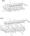
- Fig. 1 adesigned as a light-emitting bulb 1 is shown, which has a light-emitting unit 2 in the form of at least one contact strip and a support member 3, on which one or more contact surfaces and a light-emitting semiconductor element are arranged, wherein the light-emitting semiconductor element via one or more contact surfaces of the support element 3 is contacted.
- the light-emitting semiconductor elementis surrounded by an encapsulation material 4 in order to protect the light-emitting semiconductor element from environmental influences.
- a printed circuit board 5is arranged, on which in turn a contact element 6 is arranged, wherein the contact element 6 is here in the form of a female element, in particular a female connector, which has a plurality of openings 7 is formed.
- the light-emitting semiconductor elementis electrically connected to the contact element 6 via the carrier element 3, the one or more contact surfaces and the printed circuit board 5.
- the light-emitting means 1further has a mating contact element 8, which is designed here as a plug element in the form of a connector strip and has a plurality of pin contacts 9, which for forming an electrical contact between the contact element 6 and the mating contact element 8 respectively in an opening 7 of the contact element 6 can be introduced.
- the contact element 6 and the mating contact element 8are thus electrically contacted with each other via a plug connection.
- the directional arrow 10shows the movement of the Counter contact element 8 in the direction of the contact element 6 to form the connector and thus an electrical contact.
- the mating contact element 8is connected via a cable 11 to a power supply.
- Fig. 2shows a further embodiment of a luminous means 1, wherein the luminous means 1 may comprise two or more luminous element units 2a, 2b.
- Each luminous element unit 2 a, 2 bhas a respective carrier 3 a, 3 b, a light-emitting semiconductor element surrounded by an encapsulation material 4 a, 4 b, and a contact surface on which a contact element 6 a, 6 b designed as a socket element is arranged, wherein the contact element 6 a, 6 b is located directly here is arranged on the contact surface and via a cohesive connection, formed by gluing, bonding, soldering or welding, is electrically connected to the contact surface.
- a luminous means 1in the form of a light module, in which the luminous means 1 also comprises two luminous element units 2a, 2b, each luminous element unit 2a, 2b each have a support element 3a, 3b, a light emitting semiconductor element surrounded by an encapsulation material 4a, 4b and have a contact surface.
- On the contact surfaceseach formed as a plug element contact element 6a, 6b is arranged.
- the mating contact element 8is designed here as a socket element and is on a circuit board formed carrier plate 12 is arranged.
- the two contact elements 6a, 6bcan be arranged or inserted adjacent to one another on the mating contact element 8, so that here too two luminous element units 2a, 2b can be connected to one another via a mating contact element 8.
- Fig. 5shows an embodiment similar to that in FIG. 3 and FIG. 4 shown embodiment, in which case several, in particular three, mating contact elements 8a, 8b, 8c are arranged on the support plate 12 and the luminous element units 2a, 2b each have two contact elements 6a, 6b.
- the middle between the two light-emitting element units 2 a, 2 b arranged counter contact element 8 b, which is designed as a socket element,has, as in the in Fig.
Landscapes
- Engineering & Computer Science (AREA)
- General Engineering & Computer Science (AREA)
- Led Device Packages (AREA)
- Arrangement Of Elements, Cooling, Sealing, Or The Like Of Lighting Devices (AREA)
- Fastening Of Light Sources Or Lamp Holders (AREA)
- Coupling Device And Connection With Printed Circuit (AREA)
Description
Translated fromGermanDie Erfindung betrifft ein Leuchtmittel.The invention relates to a light source.
Ein derartiges Leuchtmittel kann beispielsweise als ein Leuchtmodul oder eine Leuchtpanel ausgebildet sein.Such a light source may be formed, for example, as a light module or a light panel.
Leuchtmittel weisen meist eine oder mehrere Leuchtelementeinheiten auf, die ein oder mehrere von einem Verkapselungsmaterial umgebene Licht emittierende Elemente aufweisen, die auf einem Träger, beispielsweise einem Substrat, angeordnet sind, das wiederum eine oder mehrere Kontaktflächen aufweist. Eine Ausbildung einer elektrischen Kontaktierung der Leuchtelementeinheit erfolgt meist unmittelbar über ein Anordnen von Federpins, Aufbringen eines Leitklebers oder einer Leitpaste oder Anbringen einer Crimpverbindung. Weiter ist es auch möglich ACF-gebondete Leiterplatten (ACF: Anisotropic Conductive Film; anisotrop leitfähiger Film) zu verwenden, welche eine lötfähige metallische Fläche zum Anlöten weiterer Kontaktelemente aufweisen. Derartige Kontaktierungen sind jedoch aufwändig in der Herstellung und meist unflexibel, da sie nicht mehrfach voneinander lösbar und wieder verbindbar sind.Illuminants usually have one or more light-emitting element units which have one or more light-emitting elements surrounded by an encapsulation material, which are arranged on a carrier, for example a substrate, which in turn has one or more contact surfaces. A formation of an electrical contact of the lighting element unit is usually carried out directly by arranging spring pins, applying a conductive adhesive or a conductive paste or attaching a crimp. Furthermore, it is also possible to use ACF-bonded printed circuit boards (ACF: Anisotropic Conductive Film), which have a solderable metallic surface for soldering other contact elements. However, such contacts are complex to manufacture and usually inflexible, since they are not repeatedly detachable and reconnectable.
Aus der
Eine Beleuchtungseinrichtung aus mehreren Leuchtmodulen ist aus der
Aus der
Verschiedene Ausführungsformen stellen ein Leuchtmittel zur Verfügung, bei welchem die Ausbildung einer elektrischen Kontaktierung mit einem reduzierten Aufwand erfolgen kann und zudem die elektrische Kontaktierung flexibler ausgebildet werden kann.Various embodiments provide a lighting means, in which the formation of an electrical contact can be made with a reduced effort and also the electrical contact can be made more flexible.
In verschiedenen Ausführungsformen kann ein Leuchtmittel aufweisen: mindestens eine Leuchtelementeinheit, welche einen Träger, mindestens ein auf dem Träger angeordnetes, von einem Verkapselungsmaterial umgebenes Licht emittierendes Element, mindestens eine auf dem Träger ausgebildete Kontaktfläche und mindestens ein auf der Kontaktfläche angeordnetes Kontaktelement aufweist, wobei das von einem Verkapselungsmaterial umgebene Licht emittierende Element über die Kontaktfläche mit dem Kontaktelement elektrisch verbunden ist, und mindestens ein Gegenkontaktelement, wobei das Gegenkontaktelement mit dem Kontaktelement über eine Steckverbindung elektrisch kontaktierbar ist.In various embodiments, a luminous means may comprise: at least one luminous element unit which has a support, at least one light-emitting element arranged on the support, surrounded by an encapsulation material, at least one contact surface formed on the support and at least one contact element arranged on the contact surface, wherein surrounded by an encapsulating material light-emitting element via the contact surface with the contact element electrically is connected, and at least one mating contact element, wherein the mating contact element with the contact element via a plug connection is electrically contacted.
Vorteilhafte Ausführungen und zweckmäßige Weiterbildungen der Erfindung sind in den Unteransprüchen angegeben.Advantageous embodiments and expedient developments of the invention are specified in the dependent claims.
Derartige Leuchtmittel können aus einer oder mehreren Leuchtelementeinheiten ausgebildet sein. Eine Leuchtelementeinheit kann wiederum eine oder mehrere von einem Verkapselungsmaterial umgebene Licht emittierende Elemente aufweisen, wobei die Licht emittierenden Elemente beispielsweise Leuchtdioden (light emitting diodes - LEDs) oder organische Leuchtdioden (organic light emitting diodes - OLEDs) sein können. Zur Ausbildung einer elektrischen Kontaktierung weist die Leuchtelementeinheit ein oder mehrere Kontaktelemente auf, wobei diese Kontaktelemente mit einem Gegenkontaktelement lösbar verbunden werden können, um auch hier eine elektrische Verbindung bzw. Kontaktierung auszubilden. Das Kontaktelement und das Gegenkontaktelement können über eine Steckverbindung miteinander verbunden werden. Die Steckverbindung ermöglicht eine einfache Handhabung zur Ausbildung einer elektrischen Kontaktierung, so dass die elektrische Kontaktierung ohne großen Aufwand erfolgen kann. Ferner ermöglicht die Steckverbindung, dass das Kontaktelement und das Gegenkontaktelement auch von einem (mechanisch und/oder elektrisch leitend) verbundenen Zustand in einen nicht (mechanisch und/oder elektrisch leitend) verbundenen Zustand und umgekehrt mehrfach überführbar sind, so dass die Ausbildung einer elektrischen Kontaktierung flexibel ist und dadurch mehrfach verwendet werden kann.Such lighting means can be formed from one or more light-emitting element units. A luminous element unit may in turn comprise one or more light-emitting elements surrounded by an encapsulation material, wherein the light-emitting elements may be, for example, light emitting diodes (LEDs) or organic light emitting diodes (OLEDs). To form an electrical contact, the light-emitting element unit has one or more contact elements, wherein these contact elements can be releasably connected to a mating contact element in order to form an electrical connection or contacting here as well. The contact element and the mating contact element can be connected to one another via a plug connection. The connector allows easy handling to form an electrical contact, so that the electrical contact can be done easily. Furthermore, the plug-in connection makes it possible for the contact element and the mating contact element also to be multiply transferable from a (mechanically and / or electrically conductive) connected state to a non-mechanically and / or electrically conductive state, and vice versa, so that the formation of an electrical contact is flexible and thus can be used multiple times.
Das mindestens eine Licht emittierende Element kann mindestens ein Licht emittierendes Halbleiterelement aufweisen.The at least one light-emitting element may comprise at least one light-emitting semiconductor element.
Beispielsweise ist es möglich, dass das Kontaktelement ein Buchsenelement (beispielsweise eine Buchse als ein erstes Steckverbinderteil) und das Gegenkontaktelement ein Steckerelement (beispielsweise ein Stecker als ein zweites Steckverbinderteil) sind oder das Kontaktelement ein Steckerelement und das Gegenkontaktelement ein Buchsenelement sind. Das Buchsenelement kann ein oder mehrere Öffnungen zur Aufnahme des Steckerelementes aufweisen, wobei bei mehreren Öffnungen das Buchsenelement als eine Buchsenleiste ausgebildet sein kann. Das Steckerelement kann ein oder mehrere Stiftkontaktelemente aufweisen, welche jeweils in eine Öffnung des Buchsenelementes zur Ausbildung der elektrischen Kontaktierung zwischen dem Buchsenelement und dem Steckerelement eingeführt werden können, wobei das Steckerelement als Steckerleiste bezeichnet werden kann, wenn dieses mehrere Stiftkontaktelemente aufweist. Durch die Ausbildung einer Steckverbindung mittels eines Buchsenelementes und eines Steckerelementes kann eine Steckverbindung mit einer geringen Bauhöhe ausgebildet werden. Zudem zeichnet sich eine derartige Steckverbindung durch eine einfache Handhabung aus.For example, it is possible for the contact element to be a socket element (for example a socket as a first Connector part) and the mating contact element is a plug element (for example, a plug as a second connector part) or the contact element is a plug element and the mating contact element is a socket element. The female member may have one or more openings for receiving the male member, wherein at several openings, the female member may be formed as a female connector. The plug element may have one or more pin contact elements, which may each be inserted into an opening of the socket element for forming the electrical contact between the socket element and the plug element, wherein the plug element may be referred to as a plug strip, if this has a plurality of pin contact elements. By forming a plug connection by means of a socket element and a plug element, a plug connection can be formed with a low overall height. In addition, such a connector is characterized by easy handling.
Das Kontaktelement kann mit der Kontaktfläche unmittelbar über eine stoffschlüssige Verbindung elektrisch verbunden sein. Die stoffschlüssige Verbindung kann beispielsweise durch Bonden, Löten, Schweißen oder Kleben ausgebildet sein, wodurch eine sichere und stabile Verbindung zwischen dem Kontaktelement und der Kontaktfläche ausgebildet werden kann, welche zudem die Bauhöhe einer Leuchtelementeinheit und damit auch des Leuchtmittels nicht negativ beeinflusst. Unmittelbar bedeutet hier, dass durch die stoffschlüssige Verbindung ein weiteres Bauelement angeordnet zwischen dem Kontaktelement und der Kontaktfläche optional ist.The contact element may be electrically connected to the contact surface directly via a cohesive connection. The cohesive connection can be formed for example by bonding, soldering, welding or gluing, whereby a secure and stable connection between the contact element and the contact surface can be formed, which also does not adversely affect the height of a light-emitting element and thus also of the light source. Immediately here means that by the cohesive connection another component arranged between the contact element and the contact surface is optional.
Alternativ ist es aber auch möglich, dass das Kontaktelement über eine Leiterplatte mit der Kontaktfläche elektrisch verbunden ist. Das Kontaktelement kann dann beispielsweise über eine Lötverbindung mit der Leiterplatte fest verbunden sein. Die Leiterplatte ermöglicht beispielsweise, dass über die Leiterplatte auch mehrere Kontaktelemente nebeneinander an einer oder mehreren nebeneinander angeordneten Kontaktflächen angeordnet werden können.Alternatively, it is also possible that the contact element is electrically connected via a printed circuit board with the contact surface. The contact element can then be firmly connected, for example via a solder connection with the circuit board. The circuit board allows, for example, that over the circuit board and a plurality of contact elements side by side can be arranged on one or more juxtaposed contact surfaces.
Die Leiterplatte kann eine flexible Leiterplatte sein, welche sich durch eine besonders geringe Bauhöhe und einen geringen Platzbedarf auszeichnet.The printed circuit board can be a flexible printed circuit board, which is characterized by a particularly low height and a small footprint.
Um die Verbindung des Gegenkontaktelementes mit dem Kontaktelement vor einem ungewollten Lösen zu sichern, ist es beispielsweise möglich, dass das Gegenkontaktelement an dem Kontaktelement über mindestens ein Befestigungselement lösbar verrastbar ist. Das Befestigungselement, welches beispielsweise ein Verrastelement ist und eine mechanische Befestigung zwischen dem Kontaktelement und dem Gegenkontaktelement ermöglicht, kann derart ausgebildet sein, dass es nur mittels eines Werkzeuges lösbar ist. Beispielsweise kann das Befestigungselement in Form von ein oder mehreren Rastnasen oder Widerhaken ausgebildet sein.In order to secure the connection of the mating contact element with the contact element against accidental release, it is for example possible that the mating contact element on the contact element via at least one fastener is releasably latched. The fastening element, which is for example a latching element and enables a mechanical fastening between the contact element and the mating contact element, can be designed such that it can only be detached by means of a tool. For example, the fastener may be in the form of one or more detents or barbs.
Das Leuchtmittel kann ferner derart ausgebildet sein, dass ein Gegenkontaktelement zwei oder mehr Kontaktelemente elektrisch kontaktiert. Das Gegenkontaktelement kann dadurch zwei oder mehr Kontaktelemente überspannen, wobei dadurch auch zwei oder mehr Leuchtelementeinheiten mit einem Gegenkontaktelement elektrisch leitend kontaktiert werden können. Die Ausbildung einer elektrischen Kontaktierung bei mehreren Leuchtelementeinheiten eines Leuchtmittels kann dadurch schneller und mit einem geringeren Aufwand erfolgen. Zudem kann die Anzahl der notwendigen Gegenkontaktelemente reduziert werden, wodurch das gesamte Leuchtmittel kompakter ausgebildet werden kann.The lighting means may also be designed such that a mating contact element electrically contacts two or more contact elements. The mating contact element can thereby span two or more contact elements, thereby also two or more light-emitting element units can be electrically conductively contacted with a mating contact element. The formation of an electrical contact with a plurality of lighting element units of a light source can be done faster and with less effort. In addition, the number of necessary counter contact elements can be reduced, whereby the entire lamp can be made more compact.
Weiter ist es möglich, dass mehrere Gegenkontaktelemente an einer Trägerplatte befestigt sind und die mehreren Gegenkontaktelemente mit mehreren Kontaktelementen elektrisch kontaktierbar sind. Durch diese Ausbildung können mehrere Leuchtelementeinheiten besonders kompakt aneinander gereiht angeordnet werden, indem diese beispielsweise zu Blöcken zusammengefasst werden, um ein Leuchtmittel auszubilden. Die Trägerplatte kann beispielsweise in Form einer Leiterplatte oder auch in Form eines Rahmens, auf welchem die Gegenkontaktelemente aufsitzen, zur Erhöhung der Stabilität ausgebildet sein. Erfindungsgemäß wird eine Verbindung zwischen zwei nebeneinander angeordneten Leuchtelementeinheiten eines Leuchtmittels kompakt und unmittelbar ausgebildet, indem ein Kontaktelement einer ersten Leuchtelementeinheit mit einem Gegenkontaktelement, welches mit einem Kontaktelement einer zweiten Leuchtelementeinheit elektrisch kontaktierbar ist, über einen Verbindungsbereich einstückig verbunden ist.Further, it is possible that a plurality of mating contact elements are attached to a support plate and the plurality of mating contact elements are electrically contacted with a plurality of contact elements. As a result of this design, a plurality of luminous element units can be arranged in a particularly compact arrangement in rows, for example by blocks summarized to form a light source. The support plate may be formed, for example in the form of a printed circuit board or in the form of a frame on which the counter-contact elements seat, to increase the stability. According to the invention, a connection between two adjacent luminous element units of a luminous means is formed compactly and directly by a contact element of a first luminous element unit having a mating contact element, which is electrically contacted with a contact element of a second luminous element unit, is integrally connected via a connection region.
Das Gegenkontaktelement kann mit einer Stromzuführung, beispielsweise mittels eines Kabels, verbunden sein. Weiter ist es aber auch möglich, dass zur Verbindung von zwei Leuchtelementeinheiten ein erstes Gegenkontaktelement, welches mit einem Kontaktelement einer ersten Leuchtelementeinheit verbunden ist, mit einem zweiten Gegenkontaktelement, welches mit einem Kontaktelement einer zweiten Leuchtelementeinheit verbunden ist, über geeignete Leiterelemente, wie beispielsweise ein Kabel, miteinander verbunden sind. Ferner kann das Gegenkontaktelement auf einer Leiterplatte aufgelötet und so elektrisch leitfähig mit der Leiterplatte sowie über Leiterbahnen mit weiteren Geqenkontaktelementen verbunden sein. Dies kann beispielsweise mittels der MID-Technologie (MID: molded interconnect device) erfolgen.The mating contact element can be connected to a power supply, for example by means of a cable. But it is also possible that for connecting two light-emitting element units, a first mating contact element, which is connected to a contact element of a first light-emitting element, with a second mating contact element, which is connected to a contact element of a second light-emitting unit, via suitable conductor elements, such as a cable , are interconnected. Furthermore, the mating contact element can be soldered onto a printed circuit board and thus electrically conductively connected to the printed circuit board and via printed conductors with further Geqenkontaktelementen. This can be done for example by means of the MID technology (MID: molded interconnect device).
Ausführungsbeispiele von Leuchtmitteln sind in den Figuren dargestellt und werden im Folgenden näher erläutert.Embodiments of lighting means are shown in the figures and are explained in more detail below.
Es zeigen
- Figur 1
- eine schematische Darstellung eines Leuchtmittels gemäß einer Ausführungsform;
- Figur 2
- eine schematische Darstellung eines Leuchtmittels gemäß einer weiteren Ausführungsform;
- Figur 3
- eine schematische Darstellung eines Leuchtmittels gemäß einer weiteren Ausführungsform;
- Figur 4
- eine weitere schematische Darstellung der in
Fig. 3 gezeigten Ausführungsform eines Leuchtmittels; Figur 5- eine schematische Darstellung eines Leuchtmittels gemäß einer weiteren Ausführungsform; und
Figur 6- eine schematische Darstellung eines Leuchtmittels gemäß einer weiteren Ausführungsform.
- FIG. 1
- a schematic representation of a lighting device according to an embodiment;
- FIG. 2
- a schematic representation of a lighting device according to another embodiment;
- FIG. 3
- a schematic representation of a lighting device according to another embodiment;
- FIG. 4
- another schematic representation of in
Fig. 3 shown embodiment of a light bulb; - FIG. 5
- a schematic representation of a lighting device according to another embodiment; and
- FIG. 6
- a schematic representation of a lamp according to a further embodiment.
In der folgenden ausführlichen Beschreibung wird auf die beigefügten Zeichnungen Bezug genommen, die Teil dieser bilden und in denen zur Veranschaulichung spezifische Ausführungsformen gezeigt sind, in denen die Erfindung ausgeübt werden kann. In dieser Hinsicht wird Richtungsterminologie wie etwa "oben", "unten", "vorne", "hinten", "vorderes", "hinteres", usw. mit Bezug auf die Orientierung der beschriebenen Figur(en) verwendet. Da Komponenten von Ausführungsformen in einer Anzahl verschiedener Orientierungen positioniert werden können., dient die Richtungsterminologie zur Veranschaulichung und ist auf keinerlei Weise einschränkend. Es versteht sich, dass andere Ausführungsformen benutzt und strukturelle oder logische Änderungen vorgenommen werden können, ohne von dem Schutzumfang der vorliegenden Erfindung abzuweichen. Es versteht sich, dass die Merkmale der hierin beschriebenen verschiedenen beispielhaften Ausführungsformen miteinander kombiniert werden können, sofern nicht spezifisch anders angegeben. Die folgende ausführliche Beschreibung ist deshalb nicht in einschränkendem Sinne aufzufassen, und der Schutzumfang der vorliegenden Erfindung wird durch die angefügten Ansprüche definiert.In the following detailed description, reference is made to the accompanying drawings, which form a part hereof, and in which is shown by way of illustration specific embodiments in which the invention may be practiced. In this regard, directional terminology such as "top", "bottom", "front", "back", "front", "rear", etc. is used with reference to the orientation of the described figure (s). Because components of embodiments can be positioned in a number of different orientations, the directional terminology is illustrative and is in no way limiting. It should be understood that other embodiments may be utilized and structural or logical changes may be made without departing from the scope of the present invention. It should be understood that the features of the various exemplary embodiments described herein may be combined with each other unless specifically stated otherwise. The following detailed description is therefore not to be taken in a limiting sense, and the scope of the present invention is defined by the appended claims.
Im Rahmen dieser Beschreibung werden die Begriffe "verbunden", "angeschlossen" sowie "gekoppelt" verwendet zum Beschreiben sowohl einer direkten als auch einer indirekten Verbindung, eines direkten oder indirekten Anschlusses sowie einer direkten oder indirekten Kopplung. In den Figuren werden identische oder ähnliche Elemente mit identischen Bezugszeichen versehen, soweit dies zweckmäßig ist.As used herein, the terms "connected," "connected," and "coupled" are used to describe both direct and indirect connection, direct or indirect connection, and direct or indirect coupling. In the figures, identical or similar elements are provided with identical reference numerals, as appropriate.
In
Das Leuchtmittel 1 weist ferner ein Gegenkontaktelement 8 auf, welches hier als ein Steckerelement in Form einer Steckerleiste ausgebildet ist und eine Vielzahl von Stiftkontakten 9 aufweist, die zur Ausbildung einer elektrischen Kontaktierung zwischen dem Kontaktelement 6 und dem Gegenkontaktelement 8 jeweils in eine Öffnung 7 des Kontaktelementes 6 eingeführt werden können. Das Kontaktelement 6 und das Gegenkontaktelement 8 sind somit über eine Steckverbindung elektrisch miteinander kontaktierbar. Der Richtungspfeil 10 zeigt die Bewegung des Gegenkontaktelementes 8 in Richtung des Kontaktelementes 6 zur Ausbildung der Steckverbindung und damit einer elektrischen Kontaktierung. Das Gegenkontaktelement 8 ist über ein Kabel 11 mit einer Stromzuführung verbunden.The light-emitting means 1 further has a
In
In
Claims (10)
- Lamp (1), with• at least one light-emitting element unit (2, 2a, 2b) comprising a carrier (3, 3a, 3b), at least one light emitting element arranged on the carrier (3, 3a, 3b) and surrounded by an encapsulation material (4, 4a, 4b); a contact surface formed on the carrier (3, 3a, 3b) and at least one contact element (6, 6a, 6b) formed on the contact surface on the carrier (3, 3a, 3b) wherein the at least one light emitting element surrounded by the encapsulation material (4, 4a, 4b) is electrically connected with the contact element (6, 6a, 6b) via the contact area, and• at least one counter-contact element (8, 8a, 8b, 8c), wherein the counter-contact element (8, 8a, 8b, 8c) is electrically contactable with the contact element (6, 6a, 6b) via a plug connection;• wherein the contact element (6, 6a, 6b) is a socket member formed as a socket strip and the counter-contact element (8, 8a, 8b, 8c) is a connector member formed as a connector strip comprising a plurality of contact pin elements or the contact element (6, 6a, 6b) is a connector member formed as a connector strip comprising a plurality of contact pin elements and the counter-contact element (8, 8a, 8b, 8c) is a socket member formed as a socket stripcharacterized in that
a contact element (6, 6a, 6b) of a first light-emitting element unit (2, 2a, 2b) is connected in one piece with a counter-contact element (8, 8a, 8b, 8c) that is electrically contactable with a contact element (6, 6a, 6b) of a second light-emitting element unit (2, 2a, 2b) via a connecting region (13). - Lamp (1) according to claim 1,
wherein the at least one light emitting element surrounded by an encapsulating material (4, 4a, 4b) comprises at least one semiconductor light-emitting element. - Lamp (1) according to one of claims 1 or 2,
wherein the contact element (6, 6a, 6b) is directly electrically connected with the contact surface via a cohesive connection. - Lamp (1) according to one of claims 1 or 2,
wherein the contact element (6, 6a, 6b) is electrically connected with the contact area via a printed circuit board (5b 5, 5a). - Lamp (1) according to claim 4,
wherein the circuit board (5) is a flexible printed circuit board. - Lamp (1) according to one of claims 1 to 5,
wherein the counter-contact element (8, 8a, 8b, 8c) is releasably snapable with the contact element (6, 6a, 6b) via at least one fastener. - Lamp (1) according to one of claims 1 to 6,
wherein a counter contact element (8, 8a, 8b, 8c) electrically contacts two or more contact elements (6, 6a, 6b). - Lamp (1) according to one of claims 1 to 7,
wherein a plurality of counter contact elements (8, 8a, 8b, 8c) are fastened at a carrier plate (12) and the plurality of counter contact elements (8, 8a, 8b, 8c) are electrically contacted with a plurality of contact elements (6 , 6a, 6b). - Lamp (1) according to one of claims 1 to 8,
wherein the counter-contact element (8, 8a, 8b, 8c) is connected to a power supply. - Lamp (1) according to one of claims 1 to 9,
wherein the counter-contact element (8, 8a, 8b, 8c) that is formed as one piece with the contact element (6a) forms a step shape or Z-shape, respectively.
Applications Claiming Priority (2)
| Application Number | Priority Date | Filing Date | Title |
|---|---|---|---|
| DE102013201219.5ADE102013201219A1 (en) | 2013-01-25 | 2013-01-25 | Lamp |
| PCT/EP2013/077920WO2014114419A1 (en) | 2013-01-25 | 2013-12-23 | Illuminant |
Publications (2)
| Publication Number | Publication Date |
|---|---|
| EP2948712A1 EP2948712A1 (en) | 2015-12-02 |
| EP2948712B1true EP2948712B1 (en) | 2017-06-14 |
Family
ID=50002669
Family Applications (1)
| Application Number | Title | Priority Date | Filing Date |
|---|---|---|---|
| EP13824316.7AActiveEP2948712B1 (en) | 2013-01-25 | 2013-12-23 | Illuminant |
Country Status (5)
| Country | Link |
|---|---|
| US (1) | US9945547B2 (en) |
| EP (1) | EP2948712B1 (en) |
| CN (1) | CN104956149B (en) |
| DE (1) | DE102013201219A1 (en) |
| WO (1) | WO2014114419A1 (en) |
Families Citing this family (3)
| Publication number | Priority date | Publication date | Assignee | Title |
|---|---|---|---|---|
| CN108603654B (en) | 2016-02-26 | 2020-10-27 | Oled沃克斯有限责任公司 | Detachable electrical connector for a flat lighting module |
| DE102016112104A1 (en)* | 2016-07-01 | 2018-01-04 | Osram Opto Semiconductors Gmbh | MODULAR MODULE |
| US10941930B2 (en) | 2018-11-27 | 2021-03-09 | Kichler Lighting, LLC | Radially symmetric electrical connector |
Family Cites Families (25)
| Publication number | Priority date | Publication date | Assignee | Title |
|---|---|---|---|---|
| ES2511028T3 (en)* | 1997-07-28 | 2014-10-22 | Philips Lumileds Lighting Company Llc | Lighting with strips |
| US6462669B1 (en)* | 1999-04-06 | 2002-10-08 | E. P . Survivors Llc | Replaceable LED modules |
| JP3901404B2 (en)* | 1999-08-27 | 2007-04-04 | 株式会社小糸製作所 | Vehicle lamp |
| US20030112627A1 (en)* | 2000-09-28 | 2003-06-19 | Deese Raymond E. | Flexible sign illumination apparatus, system and method |
| US6541800B2 (en)* | 2001-02-22 | 2003-04-01 | Weldon Technologies, Inc. | High power LED |
| DE10392736T5 (en)* | 2002-10-25 | 2005-07-07 | Moriyama Sangyo K.K. | light module |
| US7300173B2 (en)* | 2004-04-08 | 2007-11-27 | Technology Assessment Group, Inc. | Replacement illumination device for a miniature flashlight bulb |
| US7280288B2 (en)* | 2004-06-04 | 2007-10-09 | Cree, Inc. | Composite optical lens with an integrated reflector |
| JP5033138B2 (en)* | 2005-12-16 | 2012-09-26 | コーニンクレッカ フィリップス エレクトロニクス エヌ ヴィ | Lighting system with interconnectable lighting modules |
| JP2008263118A (en)* | 2007-04-13 | 2008-10-30 | Nec Lighting Ltd | Light emitting device |
| US7566147B2 (en)* | 2007-05-04 | 2009-07-28 | Ruud Lighting, Inc. | Multi-LED light fixture with secure arrangement for LED-array wiring |
| US7622795B2 (en)* | 2007-05-15 | 2009-11-24 | Nichepac Technology Inc. | Light emitting diode package |
| US7641379B2 (en)* | 2007-05-21 | 2010-01-05 | Cisco Technology, Inc. | Press fit electronic component |
| JP5340268B2 (en) | 2007-05-22 | 2013-11-13 | オスラム ゲーエムベーハー | LIGHTING DEVICE AND PROJECTION DEVICE PROVIDED WITH SUCH LIGHTING DEVICE |
| US7815339B2 (en)* | 2008-01-09 | 2010-10-19 | Innotec Corporation | Light module |
| DE102008034956A1 (en)* | 2008-07-25 | 2010-02-04 | Signal-Construct Gmbh | Connecting element for connecting surface mount device type LED-strips, has two contact elements provided in interior of receptacle elements and contacting strip shaped printed circuit boards in multiple poles |
| KR200448368Y1 (en) | 2009-06-15 | 2010-04-07 | 주식회사 삼진일렉스 | Pluggable LED Bulb Connector |
| US8337214B2 (en)* | 2009-11-13 | 2012-12-25 | Cree, Inc. | Electrical connectors and light emitting device package and methods of assembling the same |
| DE102009054511A1 (en) | 2009-12-10 | 2011-06-16 | Osram Gesellschaft mit beschränkter Haftung | Method for contacting a lighting device, tool for performing the method and connection element for attachment to a lighting device |
| CN102893701B (en)* | 2010-05-04 | 2016-05-04 | 吉可多公司 | LED lighting device with communication port for sending associated information |
| WO2012020013A1 (en) | 2010-08-10 | 2012-02-16 | Osram Ag | Printed circuit board having at least one semiconductor light source, support for the printed circuit board, system comprising the printed circuit board and the support, and method for mounting the printed circuit board on the support |
| WO2012096676A1 (en)* | 2011-01-14 | 2012-07-19 | Huizhou Light Engine Ltd. | Mosaic led tile |
| DE102011075161A1 (en)* | 2011-05-03 | 2012-11-08 | Osram Ag | lighting device |
| DE202011101663U1 (en)* | 2011-05-25 | 2012-08-29 | Lumberg Connect Gmbh | Connector for connecting two printed circuit boards |
| DE202012001835U1 (en)* | 2012-02-24 | 2012-03-23 | Bjb Gmbh & Co. Kg | Connection element for a light-emitting diode (LED) arranged on a printed circuit board |
- 2013
- 2013-01-25DEDE102013201219.5Apatent/DE102013201219A1/ennot_activeWithdrawn
- 2013-12-23USUS14/763,173patent/US9945547B2/enactiveActive
- 2013-12-23CNCN201380071262.0Apatent/CN104956149B/enactiveActive
- 2013-12-23EPEP13824316.7Apatent/EP2948712B1/enactiveActive
- 2013-12-23WOPCT/EP2013/077920patent/WO2014114419A1/enactiveApplication Filing
Also Published As
| Publication number | Publication date |
|---|---|
| US20150354801A1 (en) | 2015-12-10 |
| CN104956149B (en) | 2018-03-02 |
| US9945547B2 (en) | 2018-04-17 |
| CN104956149A (en) | 2015-09-30 |
| WO2014114419A1 (en) | 2014-07-31 |
| DE102013201219A1 (en) | 2014-07-31 |
| EP2948712A1 (en) | 2015-12-02 |
Similar Documents
| Publication | Publication Date | Title |
|---|---|---|
| DE102009022094B4 (en) | stacking connector | |
| DE102007008109B4 (en) | backing plate assembly | |
| DE102012020371B4 (en) | System for electrically connecting printed circuit boards | |
| DE102010029205A1 (en) | Wire / plate connector | |
| DE102006048230A1 (en) | Light-emitting diode system, method for producing such and backlighting device | |
| DE202009018730U1 (en) | Connection arrangement on printed circuit boards | |
| EP2347639B1 (en) | Illumination device comprising two printed circuit boards | |
| DE102010031588A1 (en) | Wire / plate connector | |
| EP1536525B1 (en) | Device for contacting a circuit board by means of a connector | |
| DE102012219144A1 (en) | LIGHTING DEVICE WITH AT LEAST ONE SEMICONDUCTOR LIGHT SOURCE | |
| EP2702638B1 (en) | Plug connection for directly electrically contacting a circuit board | |
| DE102013100109A1 (en) | Panel feed-through edge connector and component mounting | |
| DE102010043220A1 (en) | Lighting device and method for assembling a lighting device | |
| EP2948712B1 (en) | Illuminant | |
| AT14381U1 (en) | Connection or connection terminal as well as circuit board and lighting system | |
| DE102013214124B4 (en) | Vehicle mounted camera device | |
| DE202016105563U1 (en) | Printed circuit board assembly | |
| DE60315954T2 (en) | LAMINATED CONTACTS IN BASE | |
| DE102015101796A1 (en) | Light-emitting module and this lighting device using | |
| WO2015007904A1 (en) | Lighting device having a semiconductor light source and having a driver circuit board | |
| DE102013206728A1 (en) | lighting system | |
| DE102006009582B4 (en) | Electronic device of a vehicle, in particular an antenna amplifier or a TV tuner, with a receiving space for a connector | |
| DE102017114553A1 (en) | Organic light emitting diode and method for electrically connecting an organic light emitting diode | |
| DE1640848A1 (en) | Plug connection for flexible printed circuits | |
| DE102012011047B4 (en) | Connection component and circuit arrangement with the connection component |
Legal Events
| Date | Code | Title | Description |
|---|---|---|---|
| PUAI | Public reference made under article 153(3) epc to a published international application that has entered the european phase | Free format text:ORIGINAL CODE: 0009012 | |
| 17P | Request for examination filed | Effective date:20150410 | |
| AK | Designated contracting states | Kind code of ref document:A1 Designated state(s):AL AT BE BG CH CY CZ DE DK EE ES FI FR GB GR HR HU IE IS IT LI LT LU LV MC MK MT NL NO PL PT RO RS SE SI SK SM TR | |
| AX | Request for extension of the european patent | Extension state:BA ME | |
| DAX | Request for extension of the european patent (deleted) | ||
| GRAP | Despatch of communication of intention to grant a patent | Free format text:ORIGINAL CODE: EPIDOSNIGR1 | |
| RIC1 | Information provided on ipc code assigned before grant | Ipc:F21Y 115/15 20160101ALN20161202BHEP Ipc:F21Y 115/10 20160101ALN20161202BHEP Ipc:F21V 23/06 20060101AFI20161202BHEP Ipc:F21Y 105/10 20160101ALN20161202BHEP Ipc:F21Y 105/00 20160101ALN20161202BHEP Ipc:F21Y 101/00 20160101ALN20161202BHEP | |
| INTG | Intention to grant announced | Effective date:20170102 | |
| GRAS | Grant fee paid | Free format text:ORIGINAL CODE: EPIDOSNIGR3 | |
| GRAA | (expected) grant | Free format text:ORIGINAL CODE: 0009210 | |
| AK | Designated contracting states | Kind code of ref document:B1 Designated state(s):AL AT BE BG CH CY CZ DE DK EE ES FI FR GB GR HR HU IE IS IT LI LT LU LV MC MK MT NL NO PL PT RO RS SE SI SK SM TR | |
| REG | Reference to a national code | Ref country code:GB Ref legal event code:FG4D Free format text:NOT ENGLISH | |
| REG | Reference to a national code | Ref country code:CH Ref legal event code:EP Ref country code:AT Ref legal event code:REF Ref document number:901343 Country of ref document:AT Kind code of ref document:T Effective date:20170615 | |
| REG | Reference to a national code | Ref country code:IE Ref legal event code:FG4D Free format text:LANGUAGE OF EP DOCUMENT: GERMAN | |
| REG | Reference to a national code | Ref country code:DE Ref legal event code:R096 Ref document number:502013007519 Country of ref document:DE | |
| REG | Reference to a national code | Ref country code:NL Ref legal event code:MP Effective date:20170614 | |
| REG | Reference to a national code | Ref country code:LT Ref legal event code:MG4D | |
| PG25 | Lapsed in a contracting state [announced via postgrant information from national office to epo] | Ref country code:HR Free format text:LAPSE BECAUSE OF FAILURE TO SUBMIT A TRANSLATION OF THE DESCRIPTION OR TO PAY THE FEE WITHIN THE PRESCRIBED TIME-LIMIT Effective date:20170614 Ref country code:NO Free format text:LAPSE BECAUSE OF FAILURE TO SUBMIT A TRANSLATION OF THE DESCRIPTION OR TO PAY THE FEE WITHIN THE PRESCRIBED TIME-LIMIT Effective date:20170914 Ref country code:FI Free format text:LAPSE BECAUSE OF FAILURE TO SUBMIT A TRANSLATION OF THE DESCRIPTION OR TO PAY THE FEE WITHIN THE PRESCRIBED TIME-LIMIT Effective date:20170614 Ref country code:LT Free format text:LAPSE BECAUSE OF FAILURE TO SUBMIT A TRANSLATION OF THE DESCRIPTION OR TO PAY THE FEE WITHIN THE PRESCRIBED TIME-LIMIT Effective date:20170614 Ref country code:GR Free format text:LAPSE BECAUSE OF FAILURE TO SUBMIT A TRANSLATION OF THE DESCRIPTION OR TO PAY THE FEE WITHIN THE PRESCRIBED TIME-LIMIT Effective date:20170915 | |
| PG25 | Lapsed in a contracting state [announced via postgrant information from national office to epo] | Ref country code:SE Free format text:LAPSE BECAUSE OF FAILURE TO SUBMIT A TRANSLATION OF THE DESCRIPTION OR TO PAY THE FEE WITHIN THE PRESCRIBED TIME-LIMIT Effective date:20170614 Ref country code:BG Free format text:LAPSE BECAUSE OF FAILURE TO SUBMIT A TRANSLATION OF THE DESCRIPTION OR TO PAY THE FEE WITHIN THE PRESCRIBED TIME-LIMIT Effective date:20170914 Ref country code:LV Free format text:LAPSE BECAUSE OF FAILURE TO SUBMIT A TRANSLATION OF THE DESCRIPTION OR TO PAY THE FEE WITHIN THE PRESCRIBED TIME-LIMIT Effective date:20170614 Ref country code:NL Free format text:LAPSE BECAUSE OF FAILURE TO SUBMIT A TRANSLATION OF THE DESCRIPTION OR TO PAY THE FEE WITHIN THE PRESCRIBED TIME-LIMIT Effective date:20170614 Ref country code:RS Free format text:LAPSE BECAUSE OF FAILURE TO SUBMIT A TRANSLATION OF THE DESCRIPTION OR TO PAY THE FEE WITHIN THE PRESCRIBED TIME-LIMIT Effective date:20170614 | |
| PG25 | Lapsed in a contracting state [announced via postgrant information from national office to epo] | Ref country code:SK Free format text:LAPSE BECAUSE OF FAILURE TO SUBMIT A TRANSLATION OF THE DESCRIPTION OR TO PAY THE FEE WITHIN THE PRESCRIBED TIME-LIMIT Effective date:20170614 Ref country code:CZ Free format text:LAPSE BECAUSE OF FAILURE TO SUBMIT A TRANSLATION OF THE DESCRIPTION OR TO PAY THE FEE WITHIN THE PRESCRIBED TIME-LIMIT Effective date:20170614 Ref country code:EE Free format text:LAPSE BECAUSE OF FAILURE TO SUBMIT A TRANSLATION OF THE DESCRIPTION OR TO PAY THE FEE WITHIN THE PRESCRIBED TIME-LIMIT Effective date:20170614 Ref country code:RO Free format text:LAPSE BECAUSE OF FAILURE TO SUBMIT A TRANSLATION OF THE DESCRIPTION OR TO PAY THE FEE WITHIN THE PRESCRIBED TIME-LIMIT Effective date:20170614 | |
| PG25 | Lapsed in a contracting state [announced via postgrant information from national office to epo] | Ref country code:PL Free format text:LAPSE BECAUSE OF FAILURE TO SUBMIT A TRANSLATION OF THE DESCRIPTION OR TO PAY THE FEE WITHIN THE PRESCRIBED TIME-LIMIT Effective date:20170614 Ref country code:IS Free format text:LAPSE BECAUSE OF FAILURE TO SUBMIT A TRANSLATION OF THE DESCRIPTION OR TO PAY THE FEE WITHIN THE PRESCRIBED TIME-LIMIT Effective date:20171014 Ref country code:SM Free format text:LAPSE BECAUSE OF FAILURE TO SUBMIT A TRANSLATION OF THE DESCRIPTION OR TO PAY THE FEE WITHIN THE PRESCRIBED TIME-LIMIT Effective date:20170614 Ref country code:IT Free format text:LAPSE BECAUSE OF FAILURE TO SUBMIT A TRANSLATION OF THE DESCRIPTION OR TO PAY THE FEE WITHIN THE PRESCRIBED TIME-LIMIT Effective date:20170614 Ref country code:ES Free format text:LAPSE BECAUSE OF FAILURE TO SUBMIT A TRANSLATION OF THE DESCRIPTION OR TO PAY THE FEE WITHIN THE PRESCRIBED TIME-LIMIT Effective date:20170614 | |
| REG | Reference to a national code | Ref country code:DE Ref legal event code:R097 Ref document number:502013007519 Country of ref document:DE | |
| PLBE | No opposition filed within time limit | Free format text:ORIGINAL CODE: 0009261 | |
| STAA | Information on the status of an ep patent application or granted ep patent | Free format text:STATUS: NO OPPOSITION FILED WITHIN TIME LIMIT | |
| PG25 | Lapsed in a contracting state [announced via postgrant information from national office to epo] | Ref country code:DK Free format text:LAPSE BECAUSE OF FAILURE TO SUBMIT A TRANSLATION OF THE DESCRIPTION OR TO PAY THE FEE WITHIN THE PRESCRIBED TIME-LIMIT Effective date:20170614 | |
| 26N | No opposition filed | Effective date:20180315 | |
| REG | Reference to a national code | Ref country code:CH Ref legal event code:PL | |
| GBPC | Gb: european patent ceased through non-payment of renewal fee | Effective date:20171223 | |
| PG25 | Lapsed in a contracting state [announced via postgrant information from national office to epo] | Ref country code:SI Free format text:LAPSE BECAUSE OF FAILURE TO SUBMIT A TRANSLATION OF THE DESCRIPTION OR TO PAY THE FEE WITHIN THE PRESCRIBED TIME-LIMIT Effective date:20170614 | |
| REG | Reference to a national code | Ref country code:IE Ref legal event code:MM4A | |
| PG25 | Lapsed in a contracting state [announced via postgrant information from national office to epo] | Ref country code:MT Free format text:LAPSE BECAUSE OF FAILURE TO SUBMIT A TRANSLATION OF THE DESCRIPTION OR TO PAY THE FEE WITHIN THE PRESCRIBED TIME-LIMIT Effective date:20170614 Ref country code:LU Free format text:LAPSE BECAUSE OF NON-PAYMENT OF DUE FEES Effective date:20171223 | |
| REG | Reference to a national code | Ref country code:FR Ref legal event code:ST Effective date:20180831 | |
| REG | Reference to a national code | Ref country code:BE Ref legal event code:MM Effective date:20171231 | |
| PG25 | Lapsed in a contracting state [announced via postgrant information from national office to epo] | Ref country code:FR Free format text:LAPSE BECAUSE OF NON-PAYMENT OF DUE FEES Effective date:20180102 Ref country code:IE Free format text:LAPSE BECAUSE OF NON-PAYMENT OF DUE FEES Effective date:20171223 | |
| PG25 | Lapsed in a contracting state [announced via postgrant information from national office to epo] | Ref country code:LI Free format text:LAPSE BECAUSE OF NON-PAYMENT OF DUE FEES Effective date:20171231 Ref country code:GB Free format text:LAPSE BECAUSE OF NON-PAYMENT OF DUE FEES Effective date:20171223 Ref country code:CH Free format text:LAPSE BECAUSE OF NON-PAYMENT OF DUE FEES Effective date:20171231 Ref country code:BE Free format text:LAPSE BECAUSE OF NON-PAYMENT OF DUE FEES Effective date:20171231 | |
| PG25 | Lapsed in a contracting state [announced via postgrant information from national office to epo] | Ref country code:MC Free format text:LAPSE BECAUSE OF FAILURE TO SUBMIT A TRANSLATION OF THE DESCRIPTION OR TO PAY THE FEE WITHIN THE PRESCRIBED TIME-LIMIT Effective date:20170614 Ref country code:HU Free format text:LAPSE BECAUSE OF FAILURE TO SUBMIT A TRANSLATION OF THE DESCRIPTION OR TO PAY THE FEE WITHIN THE PRESCRIBED TIME-LIMIT; INVALID AB INITIO Effective date:20131223 | |
| PG25 | Lapsed in a contracting state [announced via postgrant information from national office to epo] | Ref country code:CY Free format text:LAPSE BECAUSE OF FAILURE TO SUBMIT A TRANSLATION OF THE DESCRIPTION OR TO PAY THE FEE WITHIN THE PRESCRIBED TIME-LIMIT Effective date:20170614 | |
| PG25 | Lapsed in a contracting state [announced via postgrant information from national office to epo] | Ref country code:MK Free format text:LAPSE BECAUSE OF FAILURE TO SUBMIT A TRANSLATION OF THE DESCRIPTION OR TO PAY THE FEE WITHIN THE PRESCRIBED TIME-LIMIT Effective date:20170614 | |
| REG | Reference to a national code | Ref country code:DE Ref legal event code:R082 Ref document number:502013007519 Country of ref document:DE Representative=s name:EPPING HERMANN FISCHER PATENTANWALTSGESELLSCHA, DE | |
| REG | Reference to a national code | Ref country code:AT Ref legal event code:MM01 Ref document number:901343 Country of ref document:AT Kind code of ref document:T Effective date:20181223 | |
| PG25 | Lapsed in a contracting state [announced via postgrant information from national office to epo] | Ref country code:TR Free format text:LAPSE BECAUSE OF FAILURE TO SUBMIT A TRANSLATION OF THE DESCRIPTION OR TO PAY THE FEE WITHIN THE PRESCRIBED TIME-LIMIT Effective date:20170614 | |
| PG25 | Lapsed in a contracting state [announced via postgrant information from national office to epo] | Ref country code:AT Free format text:LAPSE BECAUSE OF NON-PAYMENT OF DUE FEES Effective date:20181223 | |
| PG25 | Lapsed in a contracting state [announced via postgrant information from national office to epo] | Ref country code:PT Free format text:LAPSE BECAUSE OF FAILURE TO SUBMIT A TRANSLATION OF THE DESCRIPTION OR TO PAY THE FEE WITHIN THE PRESCRIBED TIME-LIMIT Effective date:20170614 | |
| PG25 | Lapsed in a contracting state [announced via postgrant information from national office to epo] | Ref country code:AL Free format text:LAPSE BECAUSE OF FAILURE TO SUBMIT A TRANSLATION OF THE DESCRIPTION OR TO PAY THE FEE WITHIN THE PRESCRIBED TIME-LIMIT Effective date:20170614 | |
| REG | Reference to a national code | Ref country code:DE Ref legal event code:R081 Ref document number:502013007519 Country of ref document:DE Owner name:PICTIVA DISPLAYS INTERNATIONAL LIMITED, IE Free format text:FORMER OWNER: OSRAM OLED GMBH, 93049 REGENSBURG, DE Ref country code:DE Ref legal event code:R082 Ref document number:502013007519 Country of ref document:DE Representative=s name:EPPING HERMANN FISCHER PATENTANWALTSGESELLSCHA, DE | |
| PGFP | Annual fee paid to national office [announced via postgrant information from national office to epo] | Ref country code:DE Payment date:20241218 Year of fee payment:12 |