EP2940789A1 - Communication device antenna - Google Patents
Communication device antennaDownload PDFInfo
- Publication number
- EP2940789A1 EP2940789A1EP14166273.4AEP14166273AEP2940789A1EP 2940789 A1EP2940789 A1EP 2940789A1EP 14166273 AEP14166273 AEP 14166273AEP 2940789 A1EP2940789 A1EP 2940789A1
- Authority
- EP
- European Patent Office
- Prior art keywords
- metal part
- metal
- communication device
- lateral side
- metal housing
- Prior art date
- Legal status (The legal status is an assumption and is not a legal conclusion. Google has not performed a legal analysis and makes no representation as to the accuracy of the status listed.)
- Withdrawn
Links
- 238000004891communicationMethods0.000titleclaimsabstractdescription22
- 239000002184metalSubstances0.000claimsabstractdescription70
- 230000005284excitationEffects0.000claimsabstractdescription20
- 230000008878couplingEffects0.000claimsabstractdescription5
- 238000010168coupling processMethods0.000claimsabstractdescription5
- 238000005859coupling reactionMethods0.000claimsabstractdescription5
- 230000005855radiationEffects0.000abstractdescription2
- 238000010586diagramMethods0.000description4
- 238000011161developmentMethods0.000description2
- 230000018109developmental processEffects0.000description2
- 238000010295mobile communicationMethods0.000description2
- 238000012356Product developmentMethods0.000description1
- 230000001419dependent effectEffects0.000description1
- 230000017525heat dissipationEffects0.000description1
- 238000000034methodMethods0.000description1
Images


Classifications
- H—ELECTRICITY
- H01—ELECTRIC ELEMENTS
- H01Q—ANTENNAS, i.e. RADIO AERIALS
- H01Q13/00—Waveguide horns or mouths; Slot antennas; Leaky-waveguide antennas; Equivalent structures causing radiation along the transmission path of a guided wave
- H01Q13/10—Resonant slot antennas
- H—ELECTRICITY
- H01—ELECTRIC ELEMENTS
- H01Q—ANTENNAS, i.e. RADIO AERIALS
- H01Q1/00—Details of, or arrangements associated with, antennas
- H01Q1/12—Supports; Mounting means
- H01Q1/22—Supports; Mounting means by structural association with other equipment or articles
- H01Q1/24—Supports; Mounting means by structural association with other equipment or articles with receiving set
- H01Q1/241—Supports; Mounting means by structural association with other equipment or articles with receiving set used in mobile communications, e.g. GSM
- H01Q1/242—Supports; Mounting means by structural association with other equipment or articles with receiving set used in mobile communications, e.g. GSM specially adapted for hand-held use
- H01Q1/243—Supports; Mounting means by structural association with other equipment or articles with receiving set used in mobile communications, e.g. GSM specially adapted for hand-held use with built-in antennas
Definitions
- the present inventionis related to a communication device antenna utilizing a metal housing for emitting and receiving radio signals of a communication device according to the pre-characterizing clause of claim 1.
- plastic housingsare mainly used by manufacturers due to cost concerns, in order to maintain basic radiation characteristics of an antenna.
- metal housingis currently brought by Apple iPhones and Macbooks. Since the metal housing has light weight, good heat dissipation, high strength, high impact resistance, good looking, anti-electromagnetic and recyclable characteristics, the metal housing is getting more and more popular. Therefore, the metal housings are mainly used in development of new generations of the mobile communication products.
- US patent No. 8,054,231 B2 disclosed by Ahn et al.teaches a metal case having a slot, which can be used as a slot antenna of a mobile device.
- the slotmay obviously ruin appearance of the metal case, and the slot needs to be arranged at a position corresponding to a specific area of the metal case. Therefore, it is important to design a proper antenna to allow electromagnetic waves to penetrate the metal case for achieving communication purposes without obviously ruining the appearance of the metal case.
- the present inventionaims at providing a communication device antenna utilizing a metal housing for emitting and receiving radio signals of a communication device.
- the claimed communication device antennacomprises a metal housing, a signal feed point, a ground point and an excitation component.
- the metal housinghas a first lateral side, a second lateral side corresponding to the first lateral side, and a connection side extended and connected between the first lateral side and the second lateral side, wherein an opening is formed and located adjacent to the connection side.
- the excitation componentis connected to the signal feed point and the ground point, wherein a coupling gap is defined between the excitation component and the connection side of the metal housing.
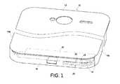
- Fig. 1 to FIG. 4are diagrams showing a communication device 10 having a metal housing 12 according to an embodiment of the present invention.
- the metal housing 12has a first lateral side 14a, a second lateral side 14b located at a position corresponding to the first lateral side 14a, and a connection side 16 extended and connected between the first lateral side 14a and the second lateral side 14b.
- Antenna arrangement of the communication device 10comprises at least a printed circuit board 20 and an excitation component 22, wherein the printed circuit board 20 comprises a signal feed point 24 and a ground point 26.
- the printed circuit board 20can be arranged in other size relative to the communication device 10. In other words, the size of the printed circuit board 20 is not limited by the figures.
- the excitation component 22comprises a first metal part 28, a second metal part 30, a third metal part 32, a fourth metal part 34 and a fifth metal part 36, wherein the first metal part 28 is connected to the signal feed point 24 of the printed circuit board; the second metal part 30 is connected to the ground point 26 of the printed circuit board 20; the third metal part 32 is located adjacent to the connection side 16 of the metal housing 12, and a coupling gap 38 is defined between the third metal part 32 and the connection side 16 of the metal housing 12.
- the fourth metal partis substantially extended and connected between the first metal part 28 and the third metal part 32 perpendicularly
- the fifth metal part 36is substantially extended and connected between the second metal part 30 and the third metal part 32 perpendicularly.
- the first metal part 28, the second metal part 30, the third metal part 32, the fourth metal part 34 and the fifth metal part 36 of the excitation component 22form an approximate circular path.
- an opening 18is formed and located adjacent to the connection side 16 of the metal housing 12.
- the opening 18comprises a first slit 40 and a second slit 42 substantially perpendicular to the first slit 40, wherein the first slit 40 is formed straight along the adjacent connection side 16 of the metal housing 12, and the second slit 42 is located adjacent to the second lateral side 14b of the metal housing 12.
- the first slit 40 and the second slit 42together form an L-shaped opening, but the opening 18 is not limited by the shape and arrangement disclosed in the embodiment of the present invention.
- the excitation component 22can work as a feeding strip for performing electromagnetic energy excitation.
- arrangement of the excitation component 22 in the figuresis one of preferred embodiments, the present invention can utilize other types of excitation components for performing electromagnetic energy excitation.
Landscapes
- Engineering & Computer Science (AREA)
- Computer Networks & Wireless Communication (AREA)
- Support Of Aerials (AREA)
Abstract
Description
- The present invention is related to a communication device antenna utilizing a metal housing for emitting and receiving radio signals of a communication device according to the pre-characterizing clause of claim 1.
- During product development processes of conventional communication devices, such as mobile communication products, plastic housings are mainly used by manufacturers due to cost concerns, in order to maintain basic radiation characteristics of an antenna. However, a trend of metal housing is currently brought by Apple iPhones and Macbooks. Since the metal housing has light weight, good heat dissipation, high strength, high impact resistance, good looking, anti-electromagnetic and recyclable characteristics, the metal housing is getting more and more popular. Therefore, the metal housings are mainly used in development of new generations of the mobile communication products. For example,
US patent No. 8,054,231 B2 disclosed by Ahn et al. teaches a metal case having a slot, which can be used as a slot antenna of a mobile device. But the slot may obviously ruin appearance of the metal case, and the slot needs to be arranged at a position corresponding to a specific area of the metal case. Therefore, it is important to design a proper antenna to allow electromagnetic waves to penetrate the metal case for achieving communication purposes without obviously ruining the appearance of the metal case. - This in mind, the present invention aims at providing a communication device antenna utilizing a metal housing for emitting and receiving radio signals of a communication device.
- This is achieved by a communication device antenna according to claim 1. The dependent claims pertain to corresponding further developments and improvements.
- As will be seen more clearly from the detailed description following below, the claimed communication device antenna comprises a metal housing, a signal feed point, a ground point and an excitation component. The metal housing has a first lateral side, a second lateral side corresponding to the first lateral side, and a connection side extended and connected between the first lateral side and the second lateral side, wherein an opening is formed and located adjacent to the connection side. The excitation component is connected to the signal feed point and the ground point, wherein a coupling gap is defined between the excitation component and the connection side of the metal housing.
- In the following, the invention is further illustrated by way of example, taking reference to the accompanying drawings thereof:
FIG. 1 is a diagram showing arrangement of a communication device according to an embodiment of the present invention,FIG. 2 is a diagram showing opening arrangement of the communication device according to the embodiment of the present invention,FIG. 3 is a diagram showing antenna arrangement of the communication device according to the embodiment of the present invention, andFIG. 4 is an enlarged view of an area A inFIG. 3 .Fig. 1 to FIG. 4 are diagrams showing acommunication device 10 having ametal housing 12 according to an embodiment of the present invention. Themetal housing 12 has a firstlateral side 14a, a secondlateral side 14b located at a position corresponding to the firstlateral side 14a, and aconnection side 16 extended and connected between the firstlateral side 14a and the secondlateral side 14b.- Antenna arrangement of the
communication device 10 comprises at least a printedcircuit board 20 and anexcitation component 22, wherein theprinted circuit board 20 comprises asignal feed point 24 and aground point 26. Please note that the printedcircuit board 20 can be arranged in other size relative to thecommunication device 10. In other words, the size of the printedcircuit board 20 is not limited by the figures. - The
excitation component 22 comprises afirst metal part 28, asecond metal part 30, athird metal part 32, afourth metal part 34 and afifth metal part 36, wherein thefirst metal part 28 is connected to thesignal feed point 24 of the printed circuit board; thesecond metal part 30 is connected to theground point 26 of the printedcircuit board 20; thethird metal part 32 is located adjacent to theconnection side 16 of themetal housing 12, and acoupling gap 38 is defined between thethird metal part 32 and theconnection side 16 of themetal housing 12. In a preferred embodiment, the fourth metal part is substantially extended and connected between thefirst metal part 28 and thethird metal part 32 perpendicularly, and thefifth metal part 36 is substantially extended and connected between thesecond metal part 30 and thethird metal part 32 perpendicularly. - The
first metal part 28, thesecond metal part 30, thethird metal part 32, thefourth metal part 34 and thefifth metal part 36 of theexcitation component 22 form an approximate circular path. - In a preferred embodiment, an
opening 18 is formed and located adjacent to theconnection side 16 of themetal housing 12. The opening 18 comprises afirst slit 40 and asecond slit 42 substantially perpendicular to thefirst slit 40, wherein thefirst slit 40 is formed straight along theadjacent connection side 16 of themetal housing 12, and thesecond slit 42 is located adjacent to the secondlateral side 14b of themetal housing 12. In a preferred embodiment, thefirst slit 40 and thesecond slit 42 together form an L-shaped opening, but theopening 18 is not limited by the shape and arrangement disclosed in the embodiment of the present invention. - According to the above arrangement, when the
communication device 10 is turned on, power at thesignal feed point 24 of the printedcircuit board 20 is fed into theexcitation component 22, and the power is further coupled to theconnection side 16 of themetal housing 12 through thecoupling gap 38, such that themetal housing 12, especially theconnection side 16 of themetal housing 12 can be utilized as a radiating strip, for transmitting and receiving radio signals of thecommunication device 10. Therefore, theexcitation component 22 can work as a feeding strip for performing electromagnetic energy excitation. Please note that arrangement of theexcitation component 22 in the figures is one of preferred embodiments, the present invention can utilize other types of excitation components for performing electromagnetic energy excitation. - According to the above illustration, efficacies and advantages of the present invention are listed as follows:
- a. appearance of the metal housing is not obviously ruined, and in contrast to the prior art, the metal housing has better appearance; and
- b. the antenna is arranged at an edge of the metal housing, and in contrast to the prior art, the antenna occupies less space.
Claims (4)
- A communication device antenna,characterized by:a metal housing (12) having a first lateral side (14a), a second lateral side (14b) corresponding to the first lateral side (14a), and a connection side (16) extended and connected between the first lateral side (14a) and the second lateral side (14b), wherein an opening (18) is formed and located adjacent to the connection side (16);a signal feed point (24);a ground point (26); andan excitation component (22) connected to the signal feed point (24) and the ground point (26), wherein a coupling gap (38) is defined between the excitation component (22) and the connection side (16) of the metal housing (12).
- The communication device antenna of claim 1,characterized in that the excitation component (22) comprises a first metal part (28), a second metal part (30), a third metal part (32), a fourth metal part (34) and a fifth metal part (36); wherein the first metal part (28) is connected to the signal feed point (24), the second metal part (30) is connected to the ground point (26), the third metal part (32) is located adjacent to the connection side (16) of the metal housing (12), the fourth metal part (34) is extended and connected between the first metal part (28) and the third metal part (32), and the fifth metal part (36) is extended and connected between the second metal part (30) and the third metal part (32).
- The communication device antenna of claim 1 or 2,characterized in that the opening (18) comprises a first slit (40) and a second slit (42), the second slit (42) is substantially perpendicular to the first slit (40), the first slit (40) is formed straight along the adjacent connection side (16) of the metal housing (12), and the second slit (42) is located adjacent to the second lateral side (14b) of the metal housing (12).
- The communication device antenna of claim 3,characterized in that the first slit (40) and the second slit (42) together form an L-shaped opening.
Priority Applications (1)
| Application Number | Priority Date | Filing Date | Title |
|---|---|---|---|
| EP14166273.4AEP2940789A1 (en) | 2014-04-28 | 2014-04-28 | Communication device antenna |
Applications Claiming Priority (1)
| Application Number | Priority Date | Filing Date | Title |
|---|---|---|---|
| EP14166273.4AEP2940789A1 (en) | 2014-04-28 | 2014-04-28 | Communication device antenna |
Publications (1)
| Publication Number | Publication Date |
|---|---|
| EP2940789A1true EP2940789A1 (en) | 2015-11-04 |
Family
ID=50588566
Family Applications (1)
| Application Number | Title | Priority Date | Filing Date |
|---|---|---|---|
| EP14166273.4AWithdrawnEP2940789A1 (en) | 2014-04-28 | 2014-04-28 | Communication device antenna |
Country Status (1)
| Country | Link |
|---|---|
| EP (1) | EP2940789A1 (en) |
Citations (7)
| Publication number | Priority date | Publication date | Assignee | Title |
|---|---|---|---|---|
| EP1950834A1 (en)* | 2007-01-24 | 2008-07-30 | Matsushita Electric Industrial Co., Ltd. | Wireless module with integrated slot antenna |
| EP2117074A1 (en)* | 2008-05-06 | 2009-11-11 | Samsung Electronics Co., Ltd. | Mobile terminal having metal case and antenna structure |
| US20130082884A1 (en)* | 2011-09-30 | 2013-04-04 | Google Inc. | Antennas for computers with conductive chassis |
| EP2621017A1 (en)* | 2012-01-27 | 2013-07-31 | Research In Motion Limited | Mobile wireless communications device including electrically conductive portable housing sections defining an antenna |
| EP2648276A1 (en)* | 2010-11-30 | 2013-10-09 | Asahi Glass Company, Limited | Window glass and antenna for vehicle |
| US20140001274A1 (en)* | 2011-04-13 | 2014-01-02 | Murata Manufacturing Co., Ltd. | Radio ic device and radio communication terminal |
| US20140078008A1 (en)* | 2012-09-19 | 2014-03-20 | Yunmo Kang | Mobile terminal |
- 2014
- 2014-04-28EPEP14166273.4Apatent/EP2940789A1/ennot_activeWithdrawn
Patent Citations (8)
| Publication number | Priority date | Publication date | Assignee | Title |
|---|---|---|---|---|
| EP1950834A1 (en)* | 2007-01-24 | 2008-07-30 | Matsushita Electric Industrial Co., Ltd. | Wireless module with integrated slot antenna |
| EP2117074A1 (en)* | 2008-05-06 | 2009-11-11 | Samsung Electronics Co., Ltd. | Mobile terminal having metal case and antenna structure |
| US8054231B2 (en) | 2008-05-06 | 2011-11-08 | Samsung Electronics Co., Ltd. | Mobile terminal having metal case and antenna structure |
| EP2648276A1 (en)* | 2010-11-30 | 2013-10-09 | Asahi Glass Company, Limited | Window glass and antenna for vehicle |
| US20140001274A1 (en)* | 2011-04-13 | 2014-01-02 | Murata Manufacturing Co., Ltd. | Radio ic device and radio communication terminal |
| US20130082884A1 (en)* | 2011-09-30 | 2013-04-04 | Google Inc. | Antennas for computers with conductive chassis |
| EP2621017A1 (en)* | 2012-01-27 | 2013-07-31 | Research In Motion Limited | Mobile wireless communications device including electrically conductive portable housing sections defining an antenna |
| US20140078008A1 (en)* | 2012-09-19 | 2014-03-20 | Yunmo Kang | Mobile terminal |
Similar Documents
| Publication | Publication Date | Title |
|---|---|---|
| US9203141B1 (en) | Communication device and antenna thereof | |
| US20150303551A1 (en) | Communication device antenna | |
| US9343802B2 (en) | Communication device and antenna thereof | |
| US9461413B2 (en) | Interference proof electrical receptacle connector | |
| EP3261173A1 (en) | Communication device and antenna assembly thereof | |
| MY190645A (en) | Antenna and electronic device including the same | |
| US20150029071A1 (en) | Antenna with multiple feed points | |
| EP4254671A3 (en) | Antenna assembly comprising antennas formed on inclined side surface of printed circuit board and electronic device comprising the same | |
| US20140313098A1 (en) | Antenna assembly and electronic device using the antenna assembly | |
| TW201622494A (en) | An assembly of circuit boards and electronic device comprising said assembly | |
| US20140085151A1 (en) | Device and communication device including antenna | |
| WO2013189375A3 (en) | Slot antenna and smart terminal | |
| US20150303550A1 (en) | Communication device antenna | |
| US20150303552A1 (en) | Communication device antenna | |
| EP2958189A1 (en) | Communication device and antenna thereof | |
| EP3012904B1 (en) | Communication device and antenna thereof | |
| JP2018121293A5 (en) | Antenna and antenna module | |
| EP2940789A1 (en) | Communication device antenna | |
| EP2940788A1 (en) | Communication device antenna | |
| EP2940790A1 (en) | Communication device antenna | |
| US9960486B2 (en) | Circuit board for an antenna assembly | |
| CN104953246B (en) | antenna of communication device | |
| TW201537827A (en) | Antenna for communication device | |
| TW200729609A (en) | Co-construction of antenna and shield having EMI against function | |
| WO2007090041A3 (en) | Rf communication device and method of operation of the device |
Legal Events
| Date | Code | Title | Description |
|---|---|---|---|
| PUAI | Public reference made under article 153(3) epc to a published international application that has entered the european phase | Free format text:ORIGINAL CODE: 0009012 | |
| AK | Designated contracting states | Kind code of ref document:A1 Designated state(s):AL AT BE BG CH CY CZ DE DK EE ES FI FR GB GR HR HU IE IS IT LI LT LU LV MC MK MT NL NO PL PT RO RS SE SI SK SM TR | |
| AX | Request for extension of the european patent | Extension state:BA ME | |
| 17P | Request for examination filed | Effective date:20151125 | |
| RBV | Designated contracting states (corrected) | Designated state(s):AL AT BE BG CH CY CZ DE DK EE ES FI FR GB GR HR HU IE IS IT LI LT LU LV MC MK MT NL NO PL PT RO RS SE SI SK SM TR | |
| STAA | Information on the status of an ep patent application or granted ep patent | Free format text:STATUS: EXAMINATION IS IN PROGRESS | |
| STAA | Information on the status of an ep patent application or granted ep patent | Free format text:STATUS: THE APPLICATION HAS BEEN WITHDRAWN | |
| 17Q | First examination report despatched | Effective date:20180606 | |
| 18W | Application withdrawn | Effective date:20180612 |