EP2932998A1 - Flexible circuit electrode array - Google Patents
Flexible circuit electrode arrayDownload PDFInfo
- Publication number
- EP2932998A1 EP2932998A1EP15164435.8AEP15164435AEP2932998A1EP 2932998 A1EP2932998 A1EP 2932998A1EP 15164435 AEP15164435 AEP 15164435AEP 2932998 A1EP2932998 A1EP 2932998A1
- Authority
- EP
- European Patent Office
- Prior art keywords
- flexible circuit
- electrode array
- polymer
- layer
- array
- Prior art date
- Legal status (The legal status is an assumption and is not a legal conclusion. Google has not performed a legal analysis and makes no representation as to the accuracy of the status listed.)
- Granted
Links
- 229920000642polymerPolymers0.000claimsabstractdescription118
- 229910052751metalInorganic materials0.000claimsabstractdescription76
- 239000002184metalSubstances0.000claimsabstractdescription76
- 210000001525retinaAnatomy0.000claimsabstractdescription66
- 230000001537neural effectEffects0.000claimsabstractdescription21
- 239000010410layerSubstances0.000claimsdescription167
- 229920001296polysiloxanePolymers0.000claimsdescription29
- BASFCYQUMIYNBI-UHFFFAOYSA-NplatinumChemical compound[Pt]BASFCYQUMIYNBI-UHFFFAOYSA-N0.000claimsdescription14
- 239000011229interlayerSubstances0.000claimsdescription12
- 239000004642PolyimideSubstances0.000claimsdescription10
- 229920001721polyimidePolymers0.000claimsdescription10
- KDLHZDBZIXYQEI-UHFFFAOYSA-NPalladiumChemical compound[Pd]KDLHZDBZIXYQEI-UHFFFAOYSA-N0.000claimsdescription8
- 150000002739metalsChemical class0.000claimsdescription7
- 229910052697platinumInorganic materials0.000claimsdescription7
- 239000010936titaniumSubstances0.000claimsdescription7
- RTAQQCXQSZGOHL-UHFFFAOYSA-NTitaniumChemical compound[Ti]RTAQQCXQSZGOHL-UHFFFAOYSA-N0.000claimsdescription6
- 229910052741iridiumInorganic materials0.000claimsdescription6
- GKOZUEZYRPOHIO-UHFFFAOYSA-Niridium atomChemical compound[Ir]GKOZUEZYRPOHIO-UHFFFAOYSA-N0.000claimsdescription6
- 229910052719titaniumInorganic materials0.000claimsdescription6
- NRTOMJZYCJJWKI-UHFFFAOYSA-NTitanium nitrideChemical compound[Ti]#NNRTOMJZYCJJWKI-UHFFFAOYSA-N0.000claimsdescription5
- 239000004020conductorSubstances0.000claimsdescription5
- HTXDPTMKBJXEOW-UHFFFAOYSA-NdioxoiridiumChemical compoundO=[Ir]=OHTXDPTMKBJXEOW-UHFFFAOYSA-N0.000claimsdescription5
- 229910000457iridium oxideInorganic materials0.000claimsdescription5
- 229920000106Liquid crystal polymerPolymers0.000claimsdescription4
- BQCADISMDOOEFD-UHFFFAOYSA-NSilverChemical compound[Ag]BQCADISMDOOEFD-UHFFFAOYSA-N0.000claimsdescription4
- PCHJSUWPFVWCPO-UHFFFAOYSA-NgoldChemical compound[Au]PCHJSUWPFVWCPO-UHFFFAOYSA-N0.000claimsdescription4
- 229910052737goldInorganic materials0.000claimsdescription4
- 239000010931goldSubstances0.000claimsdescription4
- 229910001092metal group alloyInorganic materials0.000claimsdescription4
- 229910052758niobiumInorganic materials0.000claimsdescription4
- 239000010955niobiumSubstances0.000claimsdescription4
- GUCVJGMIXFAOAE-UHFFFAOYSA-Nniobium atomChemical compound[Nb]GUCVJGMIXFAOAE-UHFFFAOYSA-N0.000claimsdescription4
- 229910052763palladiumInorganic materials0.000claimsdescription4
- 229910052709silverInorganic materials0.000claimsdescription4
- 239000004332silverSubstances0.000claimsdescription4
- 229920002725thermoplastic elastomerPolymers0.000claimsdescription4
- 239000004696Poly ether ether ketoneSubstances0.000claimsdescription3
- KJTLSVCANCCWHF-UHFFFAOYSA-NRutheniumChemical compound[Ru]KJTLSVCANCCWHF-UHFFFAOYSA-N0.000claimsdescription3
- JUPQTSLXMOCDHR-UHFFFAOYSA-Nbenzene-1,4-diol;bis(4-fluorophenyl)methanoneChemical compoundOC1=CC=C(O)C=C1.C1=CC(F)=CC=C1C(=O)C1=CC=C(F)C=C1JUPQTSLXMOCDHR-UHFFFAOYSA-N0.000claimsdescription3
- 239000003822epoxy resinSubstances0.000claimsdescription3
- 239000000203mixtureSubstances0.000claimsdescription3
- 229920000052poly(p-xylylene)Polymers0.000claimsdescription3
- 229920000647polyepoxidePolymers0.000claimsdescription3
- 229920002530polyetherether ketonePolymers0.000claimsdescription3
- 229910052703rhodiumInorganic materials0.000claimsdescription3
- 239000010948rhodiumSubstances0.000claimsdescription3
- MHOVAHRLVXNVSD-UHFFFAOYSA-Nrhodium atomChemical compound[Rh]MHOVAHRLVXNVSD-UHFFFAOYSA-N0.000claimsdescription3
- 229910052707rutheniumInorganic materials0.000claimsdescription3
- 229910001925ruthenium oxideInorganic materials0.000claimsdescription3
- WOCIAKWEIIZHES-UHFFFAOYSA-Nruthenium(iv) oxideChemical compoundO=[Ru]=OWOCIAKWEIIZHES-UHFFFAOYSA-N0.000claimsdescription3
- 229920006259thermoplastic polyimidePolymers0.000claimsdescription3
- 230000002207retinal effectEffects0.000abstractdescription35
- 230000000638stimulationEffects0.000abstractdescription24
- 230000001054cortical effectEffects0.000abstractdescription7
- 230000004438eyesightEffects0.000abstractdescription7
- 239000002861polymer materialSubstances0.000abstractdescription6
- 230000005684electric fieldEffects0.000abstractdescription4
- 230000017531blood circulationEffects0.000abstractdescription2
- 239000006185dispersionSubstances0.000abstractdescription2
- NDYMQOUYJJXCKJ-UHFFFAOYSA-N(4-fluorophenyl)-morpholin-4-ylmethanoneChemical compoundC1=CC(F)=CC=C1C(=O)N1CCOCC1NDYMQOUYJJXCKJ-UHFFFAOYSA-N0.000abstract1
- 239000000463materialSubstances0.000description38
- 238000000034methodMethods0.000description28
- 210000001519tissueAnatomy0.000description22
- 230000001681protective effectEffects0.000description21
- 229920002120photoresistant polymerPolymers0.000description20
- 210000003786scleraAnatomy0.000description20
- 210000001508eyeAnatomy0.000description16
- 239000011810insulating materialSubstances0.000description16
- 239000000758substrateSubstances0.000description16
- 238000005530etchingMethods0.000description14
- 230000003247decreasing effectEffects0.000description13
- 230000008901benefitEffects0.000description11
- 238000000151depositionMethods0.000description10
- 230000008569processEffects0.000description10
- 239000010409thin filmSubstances0.000description9
- 230000000007visual effectEffects0.000description9
- 230000001939inductive effectEffects0.000description8
- 230000006378damageEffects0.000description7
- 206010034962PhotopsiaDiseases0.000description6
- XUIMIQQOPSSXEZ-UHFFFAOYSA-NSiliconChemical compound[Si]XUIMIQQOPSSXEZ-UHFFFAOYSA-N0.000description6
- 238000004519manufacturing processMethods0.000description6
- 229910000065phospheneInorganic materials0.000description6
- 239000010703siliconSubstances0.000description6
- 229910052710siliconInorganic materials0.000description6
- 210000004027cellAnatomy0.000description5
- 239000011248coating agentSubstances0.000description5
- 238000000576coating methodMethods0.000description5
- 210000003205muscleAnatomy0.000description5
- 238000000059patterningMethods0.000description5
- 210000003161choroidAnatomy0.000description4
- 210000003477cochleaAnatomy0.000description4
- 239000011521glassSubstances0.000description4
- 238000000608laser ablationMethods0.000description4
- 230000033001locomotionEffects0.000description4
- 238000001020plasma etchingMethods0.000description4
- 229920001187thermosetting polymerPolymers0.000description4
- 239000004977Liquid-crystal polymers (LCPs)Substances0.000description3
- 206010057430Retinal injuryDiseases0.000description3
- 210000003423ankleAnatomy0.000description3
- 238000005266castingMethods0.000description3
- 238000005229chemical vapour depositionMethods0.000description3
- 230000007423decreaseEffects0.000description3
- 238000009826distributionMethods0.000description3
- 238000002474experimental methodMethods0.000description3
- 230000001771impaired effectEffects0.000description3
- 238000002513implantationMethods0.000description3
- 230000005499meniscusEffects0.000description3
- 210000000653nervous systemAnatomy0.000description3
- 210000002569neuronAnatomy0.000description3
- 238000000206photolithographyMethods0.000description3
- 238000009987spinningMethods0.000description3
- 239000012815thermoplastic materialSubstances0.000description3
- 201000004569BlindnessDiseases0.000description2
- 241000282326Felis catusSpecies0.000description2
- 208000003098Ganglion CystsDiseases0.000description2
- 208000005400Synovial CystDiseases0.000description2
- 208000027418Wounds and injuryDiseases0.000description2
- 238000013459approachMethods0.000description2
- 239000011324beadSubstances0.000description2
- 238000001312dry etchingMethods0.000description2
- 238000009713electroplatingMethods0.000description2
- 230000035876healingEffects0.000description2
- 238000010438heat treatmentMethods0.000description2
- 238000003698laser cuttingMethods0.000description2
- 210000005036nerveAnatomy0.000description2
- 108091008695photoreceptorsProteins0.000description2
- 239000011148porous materialSubstances0.000description2
- 230000009467reductionEffects0.000description2
- 229920002379silicone rubberPolymers0.000description2
- 239000007779soft materialSubstances0.000description2
- 238000000992sputter etchingMethods0.000description2
- 238000001356surgical procedureMethods0.000description2
- 238000012546transferMethods0.000description2
- 238000001039wet etchingMethods0.000description2
- 206010003694AtrophyDiseases0.000description1
- 208000002177CataractDiseases0.000description1
- 102000008186CollagenHuman genes0.000description1
- 108010035532CollagenProteins0.000description1
- 208000027534Emotional diseaseDiseases0.000description1
- 206010016654FibrosisDiseases0.000description1
- 229920000544Gore-TexPolymers0.000description1
- 208000018737Parkinson diseaseDiseases0.000description1
- XYFCBTPGUUZFHI-UHFFFAOYSA-NPhosphineChemical compoundPXYFCBTPGUUZFHI-UHFFFAOYSA-N0.000description1
- 208000037111Retinal HemorrhageDiseases0.000description1
- 208000017442Retinal diseaseDiseases0.000description1
- 208000007014Retinitis pigmentosaDiseases0.000description1
- 229920004695VICTREX™ PEEKPolymers0.000description1
- 230000004308accommodationEffects0.000description1
- 230000036982action potentialEffects0.000description1
- 230000004913activationEffects0.000description1
- 239000000853adhesiveSubstances0.000description1
- 230000001070adhesive effectEffects0.000description1
- 210000000577adipose tissueAnatomy0.000description1
- 206010064930age-related macular degenerationDiseases0.000description1
- 239000000956alloySubstances0.000description1
- 229910045601alloyInorganic materials0.000description1
- 230000037444atrophyEffects0.000description1
- 210000003050axonAnatomy0.000description1
- 230000003376axonal effectEffects0.000description1
- 229920005601base polymerPolymers0.000description1
- 239000000560biocompatible materialSubstances0.000description1
- 230000005540biological transmissionEffects0.000description1
- 230000036770blood supplyEffects0.000description1
- 210000004556brainAnatomy0.000description1
- 210000003710cerebral cortexAnatomy0.000description1
- 210000004720cerebrumAnatomy0.000description1
- 229920001436collagenPolymers0.000description1
- 230000006835compressionEffects0.000description1
- 238000007906compressionMethods0.000description1
- 239000012141concentrateSubstances0.000description1
- 238000010276constructionMethods0.000description1
- 210000005257cortical tissueAnatomy0.000description1
- 238000005520cutting processMethods0.000description1
- 230000003412degenerative effectEffects0.000description1
- 238000003618dip coatingMethods0.000description1
- 238000012377drug deliveryMethods0.000description1
- 230000000694effectsEffects0.000description1
- 238000005516engineering processMethods0.000description1
- 210000003414extremityAnatomy0.000description1
- 210000000744eyelidAnatomy0.000description1
- 230000004761fibrosisEffects0.000description1
- 239000010408filmSubstances0.000description1
- 239000004811fluoropolymerSubstances0.000description1
- 210000003128headAnatomy0.000description1
- 230000036541healthEffects0.000description1
- 239000007943implantSubstances0.000description1
- 230000001976improved effectEffects0.000description1
- 230000006872improvementEffects0.000description1
- 208000014674injuryDiseases0.000description1
- 230000003993interactionEffects0.000description1
- 210000003127kneeAnatomy0.000description1
- 210000002414legAnatomy0.000description1
- 208000002780macular degenerationDiseases0.000description1
- 239000011159matrix materialSubstances0.000description1
- 230000007246mechanismEffects0.000description1
- 239000012528membraneSubstances0.000description1
- 201000006417multiple sclerosisDiseases0.000description1
- 210000005157neural retinaAnatomy0.000description1
- 208000001749optic atrophyDiseases0.000description1
- 230000000737periodic effectEffects0.000description1
- 238000005240physical vapour depositionMethods0.000description1
- 238000007747platingMethods0.000description1
- 229920000728polyesterPolymers0.000description1
- 230000001737promoting effectEffects0.000description1
- 230000004044responseEffects0.000description1
- 210000003994retinal ganglion cellAnatomy0.000description1
- 208000032253retinal ischemiaDiseases0.000description1
- 210000001116retinal neuronAnatomy0.000description1
- 230000002441reversible effectEffects0.000description1
- 238000007789sealingMethods0.000description1
- 230000035807sensationEffects0.000description1
- 230000001953sensory effectEffects0.000description1
- 239000007787solidSubstances0.000description1
- 238000004544sputter depositionMethods0.000description1
- 230000004936stimulating effectEffects0.000description1
- 239000000126substanceSubstances0.000description1
- 238000003856thermoformingMethods0.000description1
- 229920001169thermoplasticPolymers0.000description1
- 210000000857visual cortexAnatomy0.000description1
- 230000016776visual perceptionEffects0.000description1
- 239000013585weight reducing agentSubstances0.000description1
- 230000037303wrinklesEffects0.000description1
Images


Classifications
- A—HUMAN NECESSITIES
- A61—MEDICAL OR VETERINARY SCIENCE; HYGIENE
- A61N—ELECTROTHERAPY; MAGNETOTHERAPY; RADIATION THERAPY; ULTRASOUND THERAPY
- A61N1/00—Electrotherapy; Circuits therefor
- A61N1/02—Details
- A61N1/04—Electrodes
- A61N1/05—Electrodes for implantation or insertion into the body, e.g. heart electrode
- A61N1/0526—Head electrodes
- A61N1/0543—Retinal electrodes
- A—HUMAN NECESSITIES
- A61—MEDICAL OR VETERINARY SCIENCE; HYGIENE
- A61N—ELECTROTHERAPY; MAGNETOTHERAPY; RADIATION THERAPY; ULTRASOUND THERAPY
- A61N1/00—Electrotherapy; Circuits therefor
- A61N1/02—Details
- A61N1/04—Electrodes
- A61N1/05—Electrodes for implantation or insertion into the body, e.g. heart electrode
- A61N1/0526—Head electrodes
- A61N1/0541—Cochlear electrodes
- A—HUMAN NECESSITIES
- A61—MEDICAL OR VETERINARY SCIENCE; HYGIENE
- A61N—ELECTROTHERAPY; MAGNETOTHERAPY; RADIATION THERAPY; ULTRASOUND THERAPY
- A61N1/00—Electrotherapy; Circuits therefor
- A61N1/18—Applying electric currents by contact electrodes
- A61N1/32—Applying electric currents by contact electrodes alternating or intermittent currents
- A61N1/36—Applying electric currents by contact electrodes alternating or intermittent currents for stimulation
- A61N1/36046—Applying electric currents by contact electrodes alternating or intermittent currents for stimulation of the eye
- H—ELECTRICITY
- H05—ELECTRIC TECHNIQUES NOT OTHERWISE PROVIDED FOR
- H05K—PRINTED CIRCUITS; CASINGS OR CONSTRUCTIONAL DETAILS OF ELECTRIC APPARATUS; MANUFACTURE OF ASSEMBLAGES OF ELECTRICAL COMPONENTS
- H05K1/00—Printed circuits
- H05K1/02—Details
- H05K1/0277—Bendability or stretchability details
- H05K1/028—Bending or folding regions of flexible printed circuits
- H—ELECTRICITY
- H05—ELECTRIC TECHNIQUES NOT OTHERWISE PROVIDED FOR
- H05K—PRINTED CIRCUITS; CASINGS OR CONSTRUCTIONAL DETAILS OF ELECTRIC APPARATUS; MANUFACTURE OF ASSEMBLAGES OF ELECTRICAL COMPONENTS
- H05K1/00—Printed circuits
- H05K1/02—Details
- H05K1/03—Use of materials for the substrate
- H05K1/0313—Organic insulating material
- H05K1/0353—Organic insulating material consisting of two or more materials, e.g. two or more polymers, polymer + filler, + reinforcement
- H—ELECTRICITY
- H05—ELECTRIC TECHNIQUES NOT OTHERWISE PROVIDED FOR
- H05K—PRINTED CIRCUITS; CASINGS OR CONSTRUCTIONAL DETAILS OF ELECTRIC APPARATUS; MANUFACTURE OF ASSEMBLAGES OF ELECTRICAL COMPONENTS
- H05K1/00—Printed circuits
- H05K1/02—Details
- H05K1/09—Use of materials for the conductive, e.g. metallic pattern
- H—ELECTRICITY
- H05—ELECTRIC TECHNIQUES NOT OTHERWISE PROVIDED FOR
- H05K—PRINTED CIRCUITS; CASINGS OR CONSTRUCTIONAL DETAILS OF ELECTRIC APPARATUS; MANUFACTURE OF ASSEMBLAGES OF ELECTRICAL COMPONENTS
- H05K1/00—Printed circuits
- H05K1/02—Details
- H05K1/11—Printed elements for providing electric connections to or between printed circuits
- H05K1/111—Pads for surface mounting, e.g. lay-out
- H—ELECTRICITY
- H05—ELECTRIC TECHNIQUES NOT OTHERWISE PROVIDED FOR
- H05K—PRINTED CIRCUITS; CASINGS OR CONSTRUCTIONAL DETAILS OF ELECTRIC APPARATUS; MANUFACTURE OF ASSEMBLAGES OF ELECTRICAL COMPONENTS
- H05K1/00—Printed circuits
- H05K1/02—Details
- H05K1/11—Printed elements for providing electric connections to or between printed circuits
- H05K1/115—Via connections; Lands around holes or via connections
- H—ELECTRICITY
- H05—ELECTRIC TECHNIQUES NOT OTHERWISE PROVIDED FOR
- H05K—PRINTED CIRCUITS; CASINGS OR CONSTRUCTIONAL DETAILS OF ELECTRIC APPARATUS; MANUFACTURE OF ASSEMBLAGES OF ELECTRICAL COMPONENTS
- H05K1/00—Printed circuits
- H05K1/02—Details
- H05K1/11—Printed elements for providing electric connections to or between printed circuits
- H05K1/118—Printed elements for providing electric connections to or between printed circuits specially for flexible printed circuits, e.g. using folded portions
- H—ELECTRICITY
- H05—ELECTRIC TECHNIQUES NOT OTHERWISE PROVIDED FOR
- H05K—PRINTED CIRCUITS; CASINGS OR CONSTRUCTIONAL DETAILS OF ELECTRIC APPARATUS; MANUFACTURE OF ASSEMBLAGES OF ELECTRICAL COMPONENTS
- H05K3/00—Apparatus or processes for manufacturing printed circuits
- H05K3/0011—Working of insulating substrates or insulating layers
- H05K3/0017—Etching of the substrate by chemical or physical means
- H05K3/0041—Etching of the substrate by chemical or physical means by plasma etching
- H—ELECTRICITY
- H05—ELECTRIC TECHNIQUES NOT OTHERWISE PROVIDED FOR
- H05K—PRINTED CIRCUITS; CASINGS OR CONSTRUCTIONAL DETAILS OF ELECTRIC APPARATUS; MANUFACTURE OF ASSEMBLAGES OF ELECTRICAL COMPONENTS
- H05K3/00—Apparatus or processes for manufacturing printed circuits
- H05K3/02—Apparatus or processes for manufacturing printed circuits in which the conductive material is applied to the surface of the insulating support and is thereafter removed from such areas of the surface which are not intended for current conducting or shielding
- H05K3/06—Apparatus or processes for manufacturing printed circuits in which the conductive material is applied to the surface of the insulating support and is thereafter removed from such areas of the surface which are not intended for current conducting or shielding the conductive material being removed chemically or electrolytically, e.g. by photo-etch process
- H—ELECTRICITY
- H05—ELECTRIC TECHNIQUES NOT OTHERWISE PROVIDED FOR
- H05K—PRINTED CIRCUITS; CASINGS OR CONSTRUCTIONAL DETAILS OF ELECTRIC APPARATUS; MANUFACTURE OF ASSEMBLAGES OF ELECTRICAL COMPONENTS
- H05K3/00—Apparatus or processes for manufacturing printed circuits
- H05K3/10—Apparatus or processes for manufacturing printed circuits in which conductive material is applied to the insulating support in such a manner as to form the desired conductive pattern
- H05K3/18—Apparatus or processes for manufacturing printed circuits in which conductive material is applied to the insulating support in such a manner as to form the desired conductive pattern using precipitation techniques to apply the conductive material
- H05K3/188—Apparatus or processes for manufacturing printed circuits in which conductive material is applied to the insulating support in such a manner as to form the desired conductive pattern using precipitation techniques to apply the conductive material by direct electroplating
- H—ELECTRICITY
- H05—ELECTRIC TECHNIQUES NOT OTHERWISE PROVIDED FOR
- H05K—PRINTED CIRCUITS; CASINGS OR CONSTRUCTIONAL DETAILS OF ELECTRIC APPARATUS; MANUFACTURE OF ASSEMBLAGES OF ELECTRICAL COMPONENTS
- H05K3/00—Apparatus or processes for manufacturing printed circuits
- H05K3/22—Secondary treatment of printed circuits
- H—ELECTRICITY
- H05—ELECTRIC TECHNIQUES NOT OTHERWISE PROVIDED FOR
- H05K—PRINTED CIRCUITS; CASINGS OR CONSTRUCTIONAL DETAILS OF ELECTRIC APPARATUS; MANUFACTURE OF ASSEMBLAGES OF ELECTRICAL COMPONENTS
- H05K3/00—Apparatus or processes for manufacturing printed circuits
- H05K3/38—Improvement of the adhesion between the insulating substrate and the metal
- H05K3/388—Improvement of the adhesion between the insulating substrate and the metal by the use of a metallic or inorganic thin film adhesion layer
- H—ELECTRICITY
- H05—ELECTRIC TECHNIQUES NOT OTHERWISE PROVIDED FOR
- H05K—PRINTED CIRCUITS; CASINGS OR CONSTRUCTIONAL DETAILS OF ELECTRIC APPARATUS; MANUFACTURE OF ASSEMBLAGES OF ELECTRICAL COMPONENTS
- H05K3/00—Apparatus or processes for manufacturing printed circuits
- H05K3/46—Manufacturing multilayer circuits
- H05K3/4644—Manufacturing multilayer circuits by building the multilayer layer by layer, i.e. build-up multilayer circuits
- H—ELECTRICITY
- H05—ELECTRIC TECHNIQUES NOT OTHERWISE PROVIDED FOR
- H05K—PRINTED CIRCUITS; CASINGS OR CONSTRUCTIONAL DETAILS OF ELECTRIC APPARATUS; MANUFACTURE OF ASSEMBLAGES OF ELECTRICAL COMPONENTS
- H05K2201/00—Indexing scheme relating to printed circuits covered by H05K1/00
- H05K2201/01—Dielectrics
- H05K2201/0104—Properties and characteristics in general
- H05K2201/0129—Thermoplastic polymer, e.g. auto-adhesive layer; Shaping of thermoplastic polymer
- H—ELECTRICITY
- H05—ELECTRIC TECHNIQUES NOT OTHERWISE PROVIDED FOR
- H05K—PRINTED CIRCUITS; CASINGS OR CONSTRUCTIONAL DETAILS OF ELECTRIC APPARATUS; MANUFACTURE OF ASSEMBLAGES OF ELECTRICAL COMPONENTS
- H05K2201/00—Indexing scheme relating to printed circuits covered by H05K1/00
- H05K2201/01—Dielectrics
- H05K2201/0104—Properties and characteristics in general
- H05K2201/0133—Elastomeric or compliant polymer
- H—ELECTRICITY
- H05—ELECTRIC TECHNIQUES NOT OTHERWISE PROVIDED FOR
- H05K—PRINTED CIRCUITS; CASINGS OR CONSTRUCTIONAL DETAILS OF ELECTRIC APPARATUS; MANUFACTURE OF ASSEMBLAGES OF ELECTRICAL COMPONENTS
- H05K2201/00—Indexing scheme relating to printed circuits covered by H05K1/00
- H05K2201/01—Dielectrics
- H05K2201/0137—Materials
- H05K2201/0141—Liquid crystal polymer [LCP]
- H—ELECTRICITY
- H05—ELECTRIC TECHNIQUES NOT OTHERWISE PROVIDED FOR
- H05K—PRINTED CIRCUITS; CASINGS OR CONSTRUCTIONAL DETAILS OF ELECTRIC APPARATUS; MANUFACTURE OF ASSEMBLAGES OF ELECTRICAL COMPONENTS
- H05K2201/00—Indexing scheme relating to printed circuits covered by H05K1/00
- H05K2201/01—Dielectrics
- H05K2201/0137—Materials
- H05K2201/0154—Polyimide
- H—ELECTRICITY
- H05—ELECTRIC TECHNIQUES NOT OTHERWISE PROVIDED FOR
- H05K—PRINTED CIRCUITS; CASINGS OR CONSTRUCTIONAL DETAILS OF ELECTRIC APPARATUS; MANUFACTURE OF ASSEMBLAGES OF ELECTRICAL COMPONENTS
- H05K3/00—Apparatus or processes for manufacturing printed circuits
- H05K3/0011—Working of insulating substrates or insulating layers
- H05K3/0014—Shaping of the substrate, e.g. by moulding
- Y—GENERAL TAGGING OF NEW TECHNOLOGICAL DEVELOPMENTS; GENERAL TAGGING OF CROSS-SECTIONAL TECHNOLOGIES SPANNING OVER SEVERAL SECTIONS OF THE IPC; TECHNICAL SUBJECTS COVERED BY FORMER USPC CROSS-REFERENCE ART COLLECTIONS [XRACs] AND DIGESTS
- Y10—TECHNICAL SUBJECTS COVERED BY FORMER USPC
- Y10T—TECHNICAL SUBJECTS COVERED BY FORMER US CLASSIFICATION
- Y10T29/00—Metal working
- Y10T29/49—Method of mechanical manufacture
- Y10T29/49002—Electrical device making
- Y10T29/49117—Conductor or circuit manufacturing
- Y10T29/49124—On flat or curved insulated base, e.g., printed circuit, etc.
- Y10T29/49155—Manufacturing circuit on or in base
- Y10T29/49156—Manufacturing circuit on or in base with selective destruction of conductive paths
- Y—GENERAL TAGGING OF NEW TECHNOLOGICAL DEVELOPMENTS; GENERAL TAGGING OF CROSS-SECTIONAL TECHNOLOGIES SPANNING OVER SEVERAL SECTIONS OF THE IPC; TECHNICAL SUBJECTS COVERED BY FORMER USPC CROSS-REFERENCE ART COLLECTIONS [XRACs] AND DIGESTS
- Y10—TECHNICAL SUBJECTS COVERED BY FORMER USPC
- Y10T—TECHNICAL SUBJECTS COVERED BY FORMER US CLASSIFICATION
- Y10T29/00—Metal working
- Y10T29/49—Method of mechanical manufacture
- Y10T29/49002—Electrical device making
- Y10T29/49117—Conductor or circuit manufacturing
- Y10T29/49124—On flat or curved insulated base, e.g., printed circuit, etc.
- Y10T29/49155—Manufacturing circuit on or in base
- Y10T29/49158—Manufacturing circuit on or in base with molding of insulated base
Definitions
- the present inventionis generally directed to neural stimulation and more specifically to an improved electrode array for neural stimulation.
- Foersterinvestigated the effect of electrically stimulating the exposed occipital pole of one cerebral hemisphere. He found that, when a point at the extreme occipital pole was stimulated, the patient perceived a small spot of light directly in front and motionless (a phosphene). Subsequently, Brindley and Lewin (1968) thoroughly studied electrical stimulation of the human occipital (visual) cortex. By varying the stimulation parameters, these investigators described in detail the location of the phosphenes produced relative to the specific region of the occipital cortex stimulated. These experiments demonstrated: (1) the consistent shape and position of phosphenes; (2) that increased stimulation pulse duration made phosphenes brighter; and (3) that there was no detectable interaction between neighboring electrodes which were as close as 2.4 mm apart.
- Neural tissuecan be artificially stimulated and activated by prosthetic devices that pass pulses of electrical current through electrodes on such a device.
- the passage of currentcauses changes in electrical potentials across visual neuronal membranes, which can initiate visual neuron action potentials, which are the means of information transfer in the nervous system.
- neural tissue stimulationis in the rehabilitation of the blind.
- Some forms of blindnessinvolve selective loss of the light sensitive transducers of the retina.
- Other retinal neuronsremain viable, however, and may be activated in the manner described above by placement of a prosthetic electrode device on the inner (toward the vitreous) retinal surface (epiretinal). This placement must be mechanically stable, minimize the distance between the device electrodes and the visual neurons, control the electronic field distribution and avoid undue compression of the visual neurons.
- BullaraUS Pat. No. 4,573,481 patented an electrode assembly for surgical implantation on a nerve.
- the matrixwas silicone with embedded iridium electrodes.
- the assemblyfit around a nerve to stimulate it.
- the Michelson '933 apparatusincludes an array of photosensitive devices on its surface that are connected to a plurality of electrodes positioned on the opposite surface of the device to stimulate the retina. These electrodes are disposed to form an array similar to a "bed of nails" having conductors which impinge directly on the retina to stimulate the retinal cells.
- US Patent 4,837,049 to Byersdescribes spike electrodes for neural stimulation. Each spike electrode pierces neural tissue for better electrical contact.
- US Patent 5,215,088 to Normandescribes an array of spike electrodes for cortical stimulation. Each spike pierces cortical tissue for better electrical contact.
- Retinal tacksare one way to attach a retinal electrode array to the retina.
- US Patent 5,109,844 to de Juandescribes a flat electrode array placed against the retina for visual stimulation.
- US Patent 5,935,155 to Humayundescribes a retinal prosthesis for use with the flat retinal array described in de Juan.
- One aspect of the disclosureis a flexible circuit electrode array with more than one layer of metal traces comprising: a polymer base layer; more than one layer of metal traces, separated by polymer layers, deposited on said polymer base layer, including electrodes suitable to stimulate neural tissue; and a polymer top layer deposited on said polymer base layer and said metal traces.
- Polymer materialsare useful as electrode array bodies for neural stimulation. They are particularly useful for retinal stimulation to create artificial vision, cochlear stimulation to create artificial hearing, or cortical stimulation for many purposes. Regardless of which polymer is used, the basic construction method is the same. A layer of polymer is laid down, commonly by some form of chemical vapor deposition, spinning, meniscus coating or casting. A layer of metal, preferably platinum, is applied to the polymer and patterned to create electrodes and leads for those electrodes. Patterning is commonly done by photolithographic methods. A second layer of polymer is applied over the metal layer and patterned to leave openings for the electrodes, or openings are created later by means such as laser ablation. Hence the array and its supply cable are formed of a single body. Alternatively, multiple alternating layers of metal and polymer may be applied to obtain more metal traces within a given width.
- the pressure applied against the retina, or other neural tissue, by an electrode arrayis critical. Too little pressure causes increased electrical resistance between the array and retina, along with electric field dispersion. Too much pressure may block blood flow causing retinal ischemia and hemorrhage. Pressure on the neural retina may also block axonal flow or cause neuronal atrophy leading to optic atrophy.
- Common flexible circuit fabrication techniquessuch as photolithography generally require that a flexible circuit electrode array be made flat. Since the retina is spherical, a flat array will necessarily apply more pressure near its edges, than at its center. Further, the edges of a flexible circuit polymer array may be quite sharp and cut the delicate retinal tissue. With most polymers, it is possible to curve them when heated in a mold.
- thermoplastic polymersuch as liquid crystal polymer
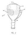
- FIG. 1shows a perspective view of the implanted portion of the preferred retinal prosthesis.
- a flexible circuit 1includes a flexible circuit electrode array 10 which is mounted by a retinal tack (not shown) or similar means to the epiretinal surface.
- the flexible circuit electrode array 10is electrically coupled by a flexible circuit cable 12, which pierces the sclera and is electrically coupled to an electronics package 14, external to the sclera.
- the electronics package 14is electrically coupled to a secondary inductive coil 16.
- the secondary inductive coil 16is made from wound wire.
- the secondary inductive coil 16may be made from a flexible circuit polymer sandwich with wire traces deposited between layers of flexible circuit polymer.
- the electronics package 14 and secondary inductive coil 16are held together by a molded body 18.
- the molded body 18may also include suture tabs 20.
- the molded body 18narrows to form a strap 22 which surrounds the sclera and holds the molded body 18, secondary inductive coil 16, and electronics package 14 in place.
- the molded body 18, suture tabs 20 and strap 22are preferably an integrated unit made of silicone elastomer.
- Silicone elastomercan be formed in a pre-curved shape to match the curvature of a typical sclera. However, silicone remains flexible enough to accommodate implantation and to adapt to variations in the curvature of an individual sclera.
- the secondary inductive coil 16 and molded body 18are preferably oval shaped.
- a strap 22can better support an oval shaped coil.
- the entire implantis attached to and supported by the sclera.
- An eyemoves constantly. The eye moves to scan a scene and also has a jitter motion to improve acuity. Even though such motion is useless in the blind, it often continues long after a person has lost their sight.
- eye motiondoes not cause any flexing which might fatigue, and eventually damage, the device.
- Fig. 2shows a side view of the implanted portion of the retinal prosthesis, in particular, emphasizing the fan tail 24.
- the secondary inductive coil 16 and molded body 18must also follow the strap 22 under the lateral rectus muscle on the side of the sclera.
- the implanted portion of the retinal prosthesisis very delicate. It is easy to tear the molded body 18 or break wires in the secondary inductive coil 16.
- the molded body 18is shaped in the form of a fan tail 24 on the end opposite the electronics package 14.
- the flexible circuit 1is a made by the following process.
- a layer of polymersuch as polyimide, fluoro-polymers, silicone or other polymers
- a support substratesuch as glass.
- Layersmay be applied by spinning, meniscus coating, casting, sputtering or other physical or chemical vapor deposition, or similar process.
- a metal layeris applied to the polymer.
- the metalis patterned by photolithographic process.
- a photo-resistis applied and patterned by photolithography followed by a wet etch of the unprotected metal.
- the metalcan be patterned by lift-off technique, laser ablation or direct write techniques.
- this metalthicker at the electrode and bond pad to improve electrical continuity. This can be accomplished through any of the above methods or electroplating. Then, the top layer of polymer is applied over the metal. Openings in the top layer for electrical contact to the electronics package 14 and the electrodes may be accomplished by laser ablation or reactive ion etching (RIE) or photolithograph and wet etch. Making the electrode openings in the top layer smaller than the electrodes promotes adhesion by avoiding delaminating around the electrode edges.
- RIEreactive ion etching
- the pressure applied against the retina by the flexible circuit electrode arrayis critical. Too little pressure causes increased electrical resistance between the array and retina. It should be noted that while the present invention is described in terms of application to the retina, the techniques described are equally applicable to many forms of neural stimulation. Application to the retina requires a convex spherical curve. Application to the cochlea requires a constant curve in one dimension and a spiral curve in the other. Application to the cerebral cortex requires a concave spherical curve. Cortical stimulation is useful for artificial vision or hearing, touch and motor control for limb prostheses, deep brain stimulation for Parkinson's disease and multiple sclerosis, and many other applications.
- a flexible circuit electrode arraybe made flat. Since the retina is spherical, a flat array will necessarily apply more pressure near its edges, than at its center. With most polymers, it is possible to curve them when heated in a mold. By applying the right amount of heat to a completed array, a curve can be induced that matches the curve of the retina. To minimize warping, it is often advantageous to repeatedly heat the flexible circuit in multiple molds, each with a decreasing radius.
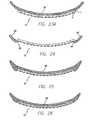
- Fig. 3illustrates a series of molds according to the preferred embodiment. Since the flexible circuit will maintain a constant length, the curvature must be slowly increased along that length. As the curvature 30 decreases in successive molds ( Figs.
- the straight line length between ends 32 and 34must decrease to keep the length along the curvature 30 constant, where mold 3E approximates the curvature of the retina or other desired neural tissue.
- the moldsprovide a further opening 36 for the flexible circuit cable 12 of the array to exit the mold without excessive curvature.
- suitable polymersinclude thermoplastic materials and thermoset materials. While a thermoplastic material will provide some stretch when heated a thermoset material will not. The successive molds are, therefore, advantageous only with a thermoplastic material. A thermoset material works as well in a single mold as it will with successive smaller molds. It should be noted that, particularly with a thermoset material, excessive curvature in three dimensions will cause the polymer material to wrinkle at the edges. This can cause damage to both the array and the retina. Hence, the amount of curvature is a compromise between the desired curvature, array surface area, and the properties of the material.
- the edges of the polymer layersare often sharp. There is a risk that the sharp edges of a flexible circuit will cut into delicate retinal tissue. It is advantageous to add a soft material, such as silicone, to the edges of a flexible circuit electrode array to round the edges and protect the retina. Silicone around the entire edge may make the flexible circuit less flexible. So, it is advantageous to provide silicone bumpers or ribs to hold the edge of the flexible circuit electrode array away from the retinal tissue. Curvature 40 fits against the retina. The leading edge 44 is most likely to cause damage and is therefore fit with molded silicone bumper. Also, edge 46, where the array lifts off the retina can cause damage and should be fit with a bumper. Any space along the side edges of curvature 40 may cause damage and may be fit with bumpers as well. It is also possible for the flexible circuit cable 12 of the electrode array to contact the retina. It is, therefore, advantageous to add periodic bumpers along the flexible circuit cable 12.
- a soft materialsuch as silicone
- a retinal flexible circuit electrode arraymust be inside the sclera in order to contact the retina.
- the sclerais cut through at the pars plana, forming a sclerotomy, and the flexible circuit passed through the sclerotomy.
- a flexible circuitis thin but wide. The more electrode wires, the wider the flexible circuit must be. It may be difficult to seal a sclerotomy over a flexible circuit wide enough to support enough wires for a high resolution array. A narrow sclerotomy is preferable.
- Fig. 5depicts a further embodiment of the part of the prosthesis shown in Fig. 4 with a fold A between the circuit electrode array 10 and the flexible circuit cable 12.
- the angle in the fold Aalso called ankle has an angle of 1°-180°, preferably 80°-120°.
- the fold Ais advantageous since it reduces tension and enables an effective attachment of the flexible electrode circuit array 10 to the retina.
- Fig. 6depicts a side view of the prosthesis insight of the eye with an angle K of the flexible circuit cable 12 and a fold A between the circuit electrode array 10 and the flexible circuit cable 12.
- the angle Kis about 45°-180°and preferably 80°-100°.
- the fold K also called kneeis advantageous because it decreases pressure which would be applied by the flexible circuit cable 10.
- Fig. 7shows the implanted portion of the retinal prosthesis including the additional feature of a gentle twist or fold 48 in the flexible circuit cable 12, where the flexible circuit cable 12 passes through the sclera (sclerotomy).
- the twistmay be a simple sharp twist, or fold 48; or it may be a longer twist, forming a tube. While the tube is rounder, it reduces the flexibility of the flexible circuit.
- a simple fold 48reduces the width of the flexible circuit with only minimal impact on flexibility.
- silicone or other pliable substancemay be used to fill the center of the tube or fold 48 formed by the twisted flexible circuit cable 12. Further it is advantageous to provide a sleeve or coating 50 that promotes healing of the sclerotomy.
- Polymerssuch as polyimide, which may be used to form the flexible circuit cable 12 and flexible circuit electrode array 10, are generally very smooth and do not promote a good bond between the flexible circuit cable 12 and scleral tissue.
- a sleeve or coating of polyester, collagen, silicone, Gore-tex or similar materialwould bond with scleral tissue and promote healing. In particular, a porous material will allow scleral tissue to grow into the pores promoting a good bond.
- the flexible circuit electrode array 10may be inserted through the sclera, behind the retina and placed between the retina and choroid to stimulate the retina subretinally.
- the stopmay be widening of the flexible circuit 1 or it may be added material such as a bumper or sleeve.
- Human visionprovides a field of view that is wider than it is high. This is partially due to fact that we have two eyes, but even a single eye provides a field of view that is approximately 90° high and 140° to 160° degrees wide. It is therefore, advantageous to provide a flexible circuit electrode array 10 that is wider than it is tall. This is equally applicable to a cortical visual array. In which case, the wider dimension is not horizontal on the visual cortex, but corresponds to horizontal in the visual scene.
- Fig. 8shows the flexible circuit electrode array prior to folding and attaching the array to the electronics package 14.
- an interconnection pad 52for connection to the electronics package 14.
- the flexible circuit electrode array 10At the other end of the flexible circuit cable 12 is the flexible circuit electrode array 10.
- an attachment point 54is provided near the flexible circuit electrode array 10.
- a retina tack(not shown) is placed through the attachment point 54 to hold the flexible circuit electrode array 10 to the retina.
- a stress relief 55is provided surrounding the attachment point 54.
- the stress relief 55may be made of a softer polymer than the flexible circuit, or it may include cutouts or thinning of the polymer to reduce the stress transmitted from the retina tack to the flexible circuit electrode array 10.
- the flexible circuit cable 12is formed in a dog leg pattern so than when it is folded at fold 48 it effectively forms a straight flexible circuit cable 12 with a narrower portion at the fold 48 for passing through the sclerotomy.
- Fig. 9shows the flexible circuit electrode array after the flexible circuit cable 12 is folded at the fold 48 to form a narrowed section.
- the flexible circuit cable 12may include a twist or tube shape as well.
- the bond pad 52 for connection to the electronics package 14 and the flexible circuit electrode array 10are on opposite side of the flexible circuit. This requires patterning, in some manner, both the base polymer layer and the top polymer layer.
- the openings for the bond pad 52 and the electrodesare on the top polymer layer and only the top polymer layer needs to be patterned.
- the narrowed portion of the flexible circuit cable 12pierces the sclera, shoulders formed by opposite ends of the narrowed portion help prevent the flexible circuit cable 12 from moving through the sclera. It may be further advantageous to add ribs or bumps of silicone or similar material to the shoulders to further prevent the flexible circuit cable 12 from moving through the sclera.
- a suture tab 56 in the flexible circuit body near the electronics packageto prevent any movement in the electronics package from being transmitted to the flexible circuit electrode array 10.
- a segment of the flexible circuit cable 12can be reinforced to permit it to be secured directly with a suture.
- a skirt 60covers the flexible circuit electrode array 10, and extends beyond its edges. It is further advantageous to include wings 62 adjacent to the attachment point 54 to spread any stress of attachment over a larger area of the retina. There are several ways of forming and bonding the skirt 60.
- the skirt 60may be directly bonded through surface activation or indirectly bonded using an adhesive.
- a flexible circuit electrode array 10may be layered using different polymers for each layer. Using too soft of a polymer may allow too much stretch and break the metal traces. Too hard of a polymer may cause damage to delicate neural tissue. Hence a relatively hard polymer, such a polyimide may be used for the bottom layer and a relatively softer polymer such a silicone may be used for the top layer including an integral skirt to protect delicate neural tissue.
- the simplest solutionis to bond the skirt 60 to the back side (away from the retina) of the flexible circuit electrode array 10 as shown in Fig. 11 . While this is the simplest mechanical solution, sharp edges of the flexible circuit electrode array 10 may contact the delicate retina tissue. Bonding the skirt to the front side (toward the retina) of the flexible circuit electrode array 10, as shown in Fig. 12 , will protect the retina from sharp edges of the flexible circuit electrode array 10. However, a window 62 must be cut in the skirt 60 around the electrodes. Further, it is more difficult to reliably bond the skirt 60 to the flexible circuit electrode array 10 with such a small contact area. This method also creates a space between the electrodes and the retina which will reduce efficiency and broaden the electrical field distribution of each electrode. Broadening the electric field distribution will limit the possible resolution of the flexible circuit electrode array 10.
- Fig. 13shows another structure where the skirt 60 is bonded to the back side of the flexible circuit electrode array 10, but curves around any sharp edges of the flexible circuit electrode array 10 to protect the retina. This gives a strong bond and protects the flexible circuit electrode array 10 edges. Because it is bonded to the back side and molded around the edges, rather than bonded to the front side, of the flexible circuit electrode array 10, the portion extending beyond the front side of the flexible circuit electrode array 10 can be much smaller. This limits any additional spacing between the electrodes and the retinal tissue.
- Fig. 14shows a flexible circuit electrode array 10 similar to Fig. 13 , with the skirt 60, flush with the front side of the flexible circuit electrode array 10 rather than extending beyond the front side. While this is more difficult to manufacture, it does not lift the electrodes off the retinal surface as with the array in Fig. 10 . It should be noted that Figs. 11, 13, and 14 show skirt 60 material along the back of the flexible circuit electrode array 10 that is not necessary other than for bonding purposes. If there is sufficient bond with the flexible circuit electrode array 10, it may advantageous to thin or remove portions of the skirt 60 material for weight reduction.
- the flexible circuit electrode array 10is manufactured in layers.
- a base layer of polymer 70is laid down, commonly by some form of chemical vapor deposition, spinning, meniscus coating or casting.
- a layer of metal 72(preferably platinum) is applied to the polymer base layer 70 and patterned to create electrodes 74 and traces for those electrodes. Patterning is commonly done by photolithographic methods.
- the electrodes 74may be built up by electroplating or similar method to increase the surface area of the electrode 74 and to allow for some reduction in the electrodes 74 over time. Similar plating may also be applied to the bond pads 52 ( fig. 8-10 ).
- a top polymer layer 76is applied over the metal layer 72 and patterned to leave openings for the electrodes 74, or openings are created later by means such as laser ablation. It is advantageous to allow an overlap of the top polymer layer 76 over the electrodes 74 to promote better adhesion between the layers, and to avoid increased electrode reduction along their edges.
- the overlapping top layerpromotes adhesion by forming a clamp to hold the metal electrode between the two polymer layers.
- multiple alternating layers of metal and polymermay be applied to obtain more metal traces within a given width.
- FIG. 16depicts the flexible circuit array 12 before it is folded and attached to the implanted portion containing an additional fold A between the flexible electrode array 12 and the flexible cable 10.
- the angle in the fold Aalso called ankle has an angle of 1°-180°, preferably 80°-120°.
- the ankleis advantageous in the process of inserting the prostheses in the eye and attaching it to the retina.
- FIG. 17depicts the flexible circuit array 12 FIG. 16 folded containing an additional fold A between the flexible electrode array 12 and the flexible cable 10.
- the flexible circuit array as shown in FIGS. 8 and 16differ by the fold A from each other.
- FIG. 18depicts a flexible circuit array of FIG. 17 with a protective skirt 60 and containing an additional fold A between the flexible electrode array and the flexible cable.
- the flexible circuit array as shown in FIGS. 10 and 18differ by the fold A from each other.
- FIG. 19depicts a top view of a flexible circuit array and flexible circuit cable showing the additional horizontal angel H between the flexible electrode array 12 and the flexible cable 10.
- the angle His from about 1° to about 90° and preferably from about 30° to about 60°.
- FIG. 20depicts another variation without the horizontal angel H between the flexible electrode array 12 and the flexible cable 10 but with an orientation of the electrodes in the flexible electrode array 12 as shown in FIG. 19 for a flexible electrode array 12.
- the grid of electrodes 13has the angle H with the flexible cable which can be the same as the angel H in the flexible electrode array 12 of FIG. 19 .
- both variation shown in FIGS. 19 and 20have the advantage that the electrodes are oriented horizontally if they are inserted into the eye. Further, both variations as shown in FIGS. 19 and 20 can also additionally contain a fold K.
- FIG. 21depicts a top view of a flexible circuit array and flexible circuit cable as shown in FIGS. 10 and 18 wherein the array contains a slit along the length axis.
- FIG. 22depicts a skirt of silicone or other pliable material as shown in Fig. 10 to 14 .
- a skirt 60covers the flexible circuit electrode array 10, and extends beyond its edges.
- the flexible circuit electrode arraycontains a slit 80 along the lengths axis.
- the skirt of silicone or other pliable materialcontains preferably at least two attachment points 81 and stress reliefs 82 are provided surrounding the attachment points 81.
- the attachment points 81are located preferably on the skirt 60 outside the flexible circuit electrode 10 and are positioned apart as far as possible from each other.
- the two tacks 81are far enough apart not to cause tenting, therefore fibrosis between the two tacks which cause a traction detachment of the retina.
- the polyimideis completely between the two tacks, which also reduce the possibility of tenting. Also, this orientation of tacks keeps the tacks away from the axons, which arise from the ganglion cells which are tried to be activated. They are away from the raffe.
- the wingsact like external tabs or strain relieves. The multiple tacks prevent rotation of the array.
- the stress relief 82may be made of a softer polymer than the flexible circuit, or it may include cutouts or thinning of the polymer to reduce the stress transmitted from the retina tack to the flexible circuit electrode array 10.
- FIG. 23depicts a flexible circuit array 10 with a protective skirt 60 bonded to the back side of the flexible circuit array 10 with a progressively decreasing radius.
- FIG. 23adepicts a flexible circuit array 10 with a protective skirt 60 bonded to the back side of the flexible circuit array 10 with a progressively decreasing radius.
- This variationshows an angle x grater than 90°. This angle is due to laser cutting. The laser cuts the polymer with an angle x. This leaves a sharp edge y. To avoid that the sharp edge come into contact with the retina the polyimide layer is turned around after the laser cutting and attached up sight down to the skirt.
- FIG. 24depicts a flexible circuit array 10 with a protective skirt 60 bonded to the front side of the flexible circuit array 10 with a progressively decreasing radius.
- FIG. 25depicts a flexible circuit array 10 with a protective skirt 60 bonded to the back side of the flexible circuit array 10 and molded around the edges of the flexible circuit array with a progressively decreasing radius.
- FIG. 26depicts a flexible circuit array 10 with a protective skirt 60 bonded to the back side of the flexible circuit array 10 and molded around the edges of the flexible circuit array and flush with the front side of the array with a progressively decreasing radius.
- FIG. 27depicts a side view of the array with a skirt 60 containing a grooved and rippled pad 56a instead a suture tab 56.
- This pad 56ahas the advantage of capturing a mattress suture 57.
- a mattress suture 57has the advantage of holding the grove or rippled pad 56a in two places as shown in FIG. 28 .
- Each suture 57is fixed on the tissue on two places 59.
- a mattress suture 57 on a grooved or rippled mattress 56atherefore provides a better stability.
- FIG. 29depicts a flexible circuit array 10 with a protective skirt 60 bonded to the front side of the flexible circuit array 10 with individual electrode 13 windows and with material, preferably silicon between the electrodes 13.
- FIG. 30depicts a flexible circuit array with a protective skirt bonded to the back side of the flexible circuit array and molded around the edges of the flexible circuit array with individual electrode windows and with material, preferably silicon between the electrodes 13.
- FIGS 31-36show several surfaces to be applied on top of the cable.
- the surfacesare thin films containing a soft polymer, preferably silicone.
- FIG. 31shows a flange 15: A flange 15 can be a solid film of material containing silicone added to the surface of the polymer containing polyimide.
- FIGS. 32-34show a ladder 15a: A ladder 15a is a flange with material removed from central portions in some shape 19.
- FIG. 35shows a skeleton structure 15b.
- a skeleton15bis a flange with material removed from perimeter portions in some shape 21.
- FIG. 36shows a structure 15c with beads 23 and bumpers 25.
- a bead 23is material added to perimeter portions of the polymer cable in some shape without material being added on the central area.
- a bumper 25can be an extended or continuous version of the beaded approach. Both approaches are helpful in preventing any possible injury of the tissue by the polymer.
- FIG. 37depicts the top view of the flexible circuit array 10 being enveloped within an insulating material 11.
- the electrode array 10comprises oval-shaped electrode array body 10, a plurality of electrodes 13 made of a conductive material, such as platinum or one of its alloys, but that can be made of any conductive biocompatible material such as iridium, iridium oxide or titanium nitride.
- the electrode array 10is enveloped within an insulating material 11 that is preferably silicone.
- "Oval-shaped" electrode array bodymeans that the body may approximate either a square or a rectangle shape, but where the corners are rounded. This shape of an electrode array is described in the U.S. Patent Application No.
- the material body 11is made of a soft material that is compatible with the electrode array body 10.
- the body 11made of silicone having hardness of about 50 or less on the Shore A scale as measured with a durometer. In an alternate embodiment the hardness is about 25 or less on the Shore A scale as measured with a durometer.
- FIG. 38depicts a cross-sectional view of the flexible circuit array 10 being enveloped within an insulating material 11. It shows how the edges of the material body 11 are lift off due to the contracted radius.
- the electrode array 10preferably also contains a fold A between the cable 12 and the electrode array 10. The angle of the fold A secures a relief of the implanted material.
- FIG. 39depicts a cross-sectional view of the flexible circuit array 10 being enveloped within an insulating material 11 with open electrodes 13 and the material 11 between the electrodes 13. This embodiment also has relief between the body 10 and the retinal R.
- FIG. 40depicts a cross-sectional view of the flexible circuit array 10 being enveloped within an insulating material 11 with open electrodes 13. This is another embodiment wherein the electrodes 13 are not separated by the material 11 but the material 11 is extended so that the electrodes 13 are prevented of direct contact with the retina R.
- FIG. 41depicts a cross-sectional view of the flexible circuit array 10being enveloped within an insulating material 11 with electrodes 13 on the surface of the material 11.
- Thisis a further embodiment with the electrode 13 on the surface of the material 11, preferably silicone.
- the embodiments shown in FIGS. 39, 40, and 41show a preferred body 11 containing silicone with the edges being lift off from the retina due to contracted radius of the silicon body 11.
- FIG. 42depicts a cross-sectional view of the flexible circuit array 10 being enveloped within an insulating material 11 with electrodes 13 on the surface of the material 11 insight the eye with an angle K in the fold of the flexible circuit cable 12 and a fold A between the circuit electrode array 10 and the flexible circuit cable 12.
- the material 11 and electrode array body 10are in intimate contact with retina R.
- the surface of electrode array body 10 in contact with retina Ris a curved surface with a contracted radius compared to the spherical curvature of retina R to minimize stress concentrations therein.
- the decreasing radius of spherical curvature of material 11 near its edgeforms edge relief that causes the edges of the body 11 to lift off the surface of retina R eliminating stress concentrations.
- the edges of body 11are strongly lifted off due to the contracted radius of the body 11.
- the edge of body 11has a rounded edge eliminating stress and cutting of retina R.
- FIG. 43shows a part of the FIG. 42 enlarged showing the electrode array 10 and the electrodes 13 enveloped by the polymer material, preferably silicone 11 being attached to the retina R.
- the electrode array 10 embedded in or enveloped by the polymer material, preferably silicone 11can be preferably produced through the following steps.
- the soft polymer material which contains siliconeis molded into the designed shape and partially hardened.
- the electrode array 10 which preferably contains polyimideis introduced and positioned in the partially hardened soft polymer containing silicone.
- the soft polymer 11 containing siliconeis fully hardened in the designed shape enveloping the electrode array 10.
- the polymer body 11has a shape with a contracted radius compared with the retina R so that the edges of the body 11 lift off from the retina R.
- FIGs. 44 - 46show application of the present invention to a cochlear prosthesis.
- Figure 44shows of front view of cochlear electrode array 110.
- the cochlear electrode array 110tapers toward the top to fit in an ever smaller cochlea and because less width is required toward the top for metal traces.
- the electrodes 174are arranged linearly along the length of the array 110. Further a skirt 160 of more compliant polymer, such as silicone surrounds the array 110.
- Figure 45is a side view of the cochlear electrode array 110.
- the cochlear electrode array 110includes a bottom polymer layer 170, metal traces 172 and a top polymer layer 176. Openings in the top polymer layer 176 define electrodes 174.
- the cochlear electrode array 110is made flat as shown if figures 44 and 13B . It is then thermoformed, as described above, into a spiral shape to approximate the shape of the cochlea, as shown in Figure 46 .
- the cochlear electrode array 110is implanted with the bottom layer 170 formed toward the outside of the curvature, and the top polymer layer 176 toward the inside of the curvature. This is opposite of the thermoforming process used for a retinal array.
- a cortical arraywould be thermoformed to curve inward like a cochlear array.
- FIG. 47 to FIG 67depict the sequence of a new process for producing a flexible circuit electrode array.
- the substrate S in that processcan be silicon or glass.
- the polymercan be polyimide, thermoplastic polyimide, silicone, parylene, LCP polymers (Imidex), epoxy resin, PEEK (Victrex), TPE (Thermoplastic elastomer) or mixtures thereof.
- the metalscan be titanium, platinum, palladium, iridium, gold, silver, niobium, titanium nitride, iridium oxide, ruthenium, ruthenium oxide, rhodium or other biocompatible metals or metal alloys or metal layers.
- FIG. 47depicts a cross-sectional view of substrate, comprising glass or silicon.
- FIG. 48depicts a cross-sectional view of the substrate and a layer of polymer P deposited on the substrate. The polymer can be deposited by spi- or dip coating or any other known method.
- FIG. 49depicts a cross-sectional view of the substrate with photoresist PR deposited on the polymer.
- FIG. 50depicts a cross-sectional view of the layer structure and photoresist PR after being exposed and developed. The developing process includes irradiation of photoresist through a template mask and removing the developed parts of the photoresist.
- FIG. 51depicts a cross-sectional view of the layer structure after polymer etching.
- FIG. 52depicts a cross-sectional view of the layer structure after stripping the photoresist PR.
- FIG. 53depicts a cross-sectional view of the layer structure after depositing thin film metals M.
- FIG. 54depicts a cross-sectional view of the layer M structure after depositing a photoresist layer PR on the thin film M.
- the metal thin filmcan contain titanium, platinum, palladium, iridium, gold, silver, niobium, titanium nitride, iridium oxide or other biocompatible metals or metal alloys or metal layers.
- An adhesion layer containing for example Tican be applied on top and bottom of the thin metal layer M.
- FIG. 55depicts a cross-sectional view of the layer structure and photoresist after being exposed and developed (see for example arrow).
- FIG. 56depicts a cross-sectional view of the layer structure after etching the thin film metal layer M by wet or dry etching (see for example arrow).
- FIG. 57depicts a cross-sectional view of the layer structure after stripping the photoresist PR.
- FIG. 58depicts a cross-sectional view of the layer structure after applying a top polymer layer P2.
- FIG. 59depicts a cross-sectional view of the layer structure after applying a photoresist layer on the top polymer layer.
- FIG. 60depicts a cross-sectional view of the layer structure and photoresist PR after being exposed and developed (see for example arrow).
- FIG. 61depicts a cross-sectional view of the layer structure after etching the top polymer layer P2 (see for example arrow).
- FIG. 62depicts a cross-sectional view of the layer structure after stripping the photoresist.
- FIG. 63depicts a cross-sectional view of the layer structure after releasing the structure from the substrate.
- FIG. 64depicts a cross-sectional view of the layer structure turned upside down and applied on a new substrate S2.
- FIG. 65depicts a cross-sectional view of the layer structure after etching down the polymer layer to the metal layer.
- FIG. 66depicts a cross-sectional view of the layer structure with deeper etching of the polymer to obtain protruding contacts.
- FIG. 67depicts a cross-sectional view of the layer structure after releasing the structure from the substrate.
- FIG. 68depicts a top view of a part of the flexible electrode array.
- Fig. 69depicts a cross-sectional view of the layer structure with deeper etching of the polymer to obtain protruding contacts PC.
- the protruding contactshave a larger surface and that is an advantage versus flat surface.
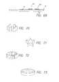
- Figs. 70 to 73show other electrode geometries as required to maximize charge uniformity or surface area or contact with tissue, for example to improve stimulus location. Circle shapes, star shapes, square shapes and rings are shown in the electrode array. Each of the shapes can contain overlapping edges and mesh grids. This presents a series of new electrode geometries that control charge transfer characteristics by the strategic use of edges and corners to concentrate current delivery. These designs are an improvement on conventional surface electrode designs which are typically circles.
- Fig. 70depicts a top view of a cluster of column shaped electrodes.
- Fig. 71depicts a top view of a star shaped electrode having a high ratio of parameter length to surface area.
- Fig. 72depicts a top view of a cluster of a column shaped electrode having a high ratio of parameter length to surface area.
- Fig. 73depicts a top view of an annular shaped electrode.
- Figs. 74 to 76show a cross-section of multilayer structure.
- the traces (metal)are in more than one layer, preferably two or three layers.
- This variationallows a less broad conducting part of the electrode array.
- the advantageis that the conducting density is increased.
- the conducting partcan be made thinner by slightly increase of the depth. The increase of the depth has only minor influence on the flexibility of the conducting part.
- Fig. 76shows filled via leading into a conducting pad. The current enters the electrode through via in the center and not at the edge. If the current is led to the electrode at the edge and the electrode starts to dissolve at the edge to the insulating material it leads to a faster break up of the conductivity.
- the advantage of the present multilayeris that the conductivity stays stable because even if the electrode starts to dissolve at the edge to the insulating material the conductivity stays stable until the electrode dissolves completely towards the center.
- Viascan be used to connect traces on different metal layers or to connect an electrode to a metal a trace.
- Fig. 74depicts a cross-sectional view of a multilayer structure.
- ITshows as an example two layers of traces T and T2.
- Trace Thas a direct contact with an electrode.
- Trace T2also has a direct contact to the electrode E.
- Fig. 75 and Fig. 75Aboth depict a cross-sectional view of a multilayer structure with inter layer vias. Vias allow connections between multiple conductor layer, here metal traces.
- Fig. 75 and Fig. 75Ashow that via passes the current through the center of the electrode and not from the edge of the electrode. This has a certain advantage because the edge of the electrode has the tendency to dissolve faster.
- Fig. 76depicts a cross-sectional view of interlayer vias used to bridge traces containing via in the trace.
- Fig. 76Adepicts a top view of interlayer vias used to bridge traces.
- This processcould be easily adapted to a multi-metal layer electrode array or similar metal and polymer structures that need to have metal contacts or openings on both sides of the structure.
Landscapes
- Engineering & Computer Science (AREA)
- Health & Medical Sciences (AREA)
- Microelectronics & Electronic Packaging (AREA)
- Manufacturing & Machinery (AREA)
- General Health & Medical Sciences (AREA)
- Biomedical Technology (AREA)
- Nuclear Medicine, Radiotherapy & Molecular Imaging (AREA)
- Radiology & Medical Imaging (AREA)
- Life Sciences & Earth Sciences (AREA)
- Animal Behavior & Ethology (AREA)
- Public Health (AREA)
- Veterinary Medicine (AREA)
- Ophthalmology & Optometry (AREA)
- Cardiology (AREA)
- Heart & Thoracic Surgery (AREA)
- Otolaryngology (AREA)
- Physics & Mathematics (AREA)
- Plasma & Fusion (AREA)
- Chemical & Material Sciences (AREA)
- Inorganic Chemistry (AREA)
- Prostheses (AREA)
Abstract
Description
- This Application claims the benefit of
U.S. Provisional Application No. 60/856,455 U.S. Application No. 11/821,328, filed June 21, 2006 U.S. Provisional Application No. 60/774,407 U.S. Provisional Application No. 60/815,311 U.S. Application No. 11/413,689, filed April 28, 2006 U.S. Application No. 11/207,644, filed August 19, 2005 U.S. Provisional Application No. 60/676,008 - This invention was made with government support under grant No. R24EY12893-01, awarded by the National Institutes of Health. The government has certain rights in the invention.
- The present invention is generally directed to neural stimulation and more specifically to an improved electrode array for neural stimulation.
- In 1755 LeRoy passed the discharge of a Leyden jar through the orbit of a man who was blind from cataract and the patient saw "flames passing rapidly downwards." Ever since, there has been a fascination with electrically elicited visual perception. The general concept of electrical stimulation of retinal cells to produce these flashes of light or phosphenes has been known for quite some time. Based on these general principles, some early attempts at devising prostheses for aiding the visually impaired have included attaching electrodes to the head or eyelids of patients. While some of these early attempts met with some limited success, these early prosthetic devices were large, bulky and could not produce adequate simulated vision to truly aid the visually impaired.
- In the early 1930's, Foerster investigated the effect of electrically stimulating the exposed occipital pole of one cerebral hemisphere. He found that, when a point at the extreme occipital pole was stimulated, the patient perceived a small spot of light directly in front and motionless (a phosphene). Subsequently, Brindley and Lewin (1968) thoroughly studied electrical stimulation of the human occipital (visual) cortex. By varying the stimulation parameters, these investigators described in detail the location of the phosphenes produced relative to the specific region of the occipital cortex stimulated. These experiments demonstrated: (1) the consistent shape and position of phosphenes; (2) that increased stimulation pulse duration made phosphenes brighter; and (3) that there was no detectable interaction between neighboring electrodes which were as close as 2.4 mm apart.
- As intraocular surgical techniques have advanced, it has become possible to apply stimulation on small groups and even on individual retinal cells to generate focused phosphenes through devices implanted within the eye itself. This has sparked renewed interest in developing methods and apparati to aid the visually impaired. Specifically, great effort has been expended in the area of intraocular retinal prosthesis devices in an effort to restore vision in cases where blindness is caused by photoreceptor degenerative retinal diseases; such as retinitis pigmentosa and age related macular degeneration which affect millions of people worldwide.
- Neural tissue can be artificially stimulated and activated by prosthetic devices that pass pulses of electrical current through electrodes on such a device. The passage of current causes changes in electrical potentials across visual neuronal membranes, which can initiate visual neuron action potentials, which are the means of information transfer in the nervous system.
- Based on this mechanism, it is possible to input information into the nervous system by coding the sensory information as a sequence of electrical pulses which are relayed to the nervous system via the prosthetic device. In this way, it is possible to provide artificial sensations including vision.
- One typical application of neural tissue stimulation is in the rehabilitation of the blind. Some forms of blindness involve selective loss of the light sensitive transducers of the retina. Other retinal neurons remain viable, however, and may be activated in the manner described above by placement of a prosthetic electrode device on the inner (toward the vitreous) retinal surface (epiretinal). This placement must be mechanically stable, minimize the distance between the device electrodes and the visual neurons, control the electronic field distribution and avoid undue compression of the visual neurons.
- In
1986, Bullara (US Pat. No. 4,573,481 ) patented an electrode assembly for surgical implantation on a nerve. The matrix was silicone with embedded iridium electrodes. The assembly fit around a nerve to stimulate it. - Dawson and Radtke stimulated cat's retina by direct electrical stimulation of the retinal ganglion cell layer. These experimenters placed nine and then fourteen electrodes upon the inner retinal layer (i.e., primarily the ganglion cell layer) of two cats. Their experiments suggested that electrical stimulation of the retina with 30 to 100 µA current resulted in visual cortical responses. These experiments were carried out with needle-shaped electrodes that penetrated the surface of the retina (see also
US Pat. No. 4,628,933 to Michelson ). - The Michelson '933 apparatus includes an array of photosensitive devices on its surface that are connected to a plurality of electrodes positioned on the opposite surface of the device to stimulate the retina. These electrodes are disposed to form an array similar to a "bed of nails" having conductors which impinge directly on the retina to stimulate the retinal cells.
US Patent 4,837,049 to Byers describes spike electrodes for neural stimulation. Each spike electrode pierces neural tissue for better electrical contact.US Patent 5,215,088 to Norman describes an array of spike electrodes for cortical stimulation. Each spike pierces cortical tissue for better electrical contact. - The art of implanting an intraocular prosthetic device to electrically stimulate the retina was advanced with the introduction of retinal tacks in retinal surgery. De Juan, et al. at Duke University Eye Center inserted retinal tacks into retinas in an effort to reattach retinas that had detached from the underlying choroid, which is the source of blood supply for the outer retina and thus the photoreceptors. See, e.g.,E. de Juan, et al., 99 Am. J. Ophthalmol. 272 (1985). These retinal tacks have proved to be biocompatible and remain embedded in the retina, and choroid/sclera, effectively pinning the retina against the choroid and the posterior aspects of the globe. Retinal tacks are one way to attach a retinal electrode array to the retina.
US Patent 5,109,844 to de Juan describes a flat electrode array placed against the retina for visual stimulation.US Patent 5,935,155 to Humayun describes a retinal prosthesis for use with the flat retinal array described in de Juan. - One aspect of the disclosure is a flexible circuit electrode array with more than one layer of metal traces comprising: a polymer base layer; more than one layer of metal traces, separated by polymer layers, deposited on said polymer base layer, including electrodes suitable to stimulate neural tissue; and a polymer top layer deposited on said polymer base layer and said metal traces.
- The novel features of the invention are set forth with particularity in the appended claims. The invention will be best understood from the following description when read in conjunction with the accompanying drawings.
FIG. 1 is a perspective view of the implanted portion of the preferred retinal prosthesis.FIG. 2 is a side view of the implanted portion of the preferred retinal prosthesis showing the fan tail in more detail.FIG. 3A - 3E depict molds for forming the flexible circuit array in a curve.FIG. 4 depicts an alternate view of the invention with ribs to help maintain curvature and prevent retinal damage.FIG. 5 depicts an alternate view of the invention with ribs to help maintain curvature and prevent retinal damage fold of the flexible circuit cable and a fold A between the circuit electrode array and the flexible circuit cable.FIG. 6 depicts a cross-sectional view of the prosthesis shown insight of the eye with an angle in the fold of the flexible circuit cable and a fold between the circuit electrode array and the flexible circuit cable.FIG. 7 depicts the implanted portion including a twist in the array to reduce the width of a sclerotomy and a sleeve to promote sealing of the sclerotomy.FIG. 8 depicts the flexible circuit array before it is folded and attached to the implanted portion.FIG. 9 depicts the flexible circuit array folded.FIG. 10 depicts a flexible circuit array with a protective skirt.FIG. 11 depicts a flexible circuit array with a protective skirt bonded to the back side of the flexible circuit array.FIG. 12 depicts a flexible circuit array with a protective skirt bonded to the front side of the flexible circuit array.FIG. 13 depicts a flexible circuit array with a protective skirt bonded to the back side of the flexible circuit array and molded around the edges of the flexible circuit array.FIG. 14 depicts a flexible circuit array with a protective skirt bonded to the back side of the flexible circuit array and molded around the edges of the flexible circuit array and flush with the front side of the array.FIG. 15 is an enlarged view of a single electrode within the flexible circuit electrode array.FIG. 16 depicts the flexible circuit array before it is folded and attached to the implanted portion containing an additional fold between the flexible electrode array and the flexible cable.FIG. 17 depicts the flexible circuit array ofFIG. 16 folded containing an additional fold between the flexible electrode array and the flexible cable.FIG. 18 depicts a flexible circuit array ofFIG. 17 with a protective skirt and containing an additional fold between the flexible electrode array and the flexible cable.FIG. 19 depicts a top view of a flexible circuit array and flexible circuit cable showing an additional horizontal angel between the flexible electrode array and the flexible cable.FIG. 20 depicts another variation without the horizontal angel between the flexible electrode array and the flexible cable but with an orientation of the electrodes in the flexible electrode array as shown for the variation inFIG. 19 .FIG. 21 depicts a top view of a flexible circuit array and flexible circuit cable wherein the array contains a slit along the length axis.FIG. 22 depicts a top view of a flexible circuit array and flexible circuit cable wherein the array contains a slit along the length axis with a two attachment points.FIG. 23 depicts a flexible circuit array with a protective skirt bonded to the back side of the flexible circuit array with a progressively decreasing radius.FIG. 23a depicts a variation of a flexible circuit array with a protective skirt bonded to the back side of the flexible circuit array with a progressively decreasing radius.FIG. 24 depicts a flexible circuit array with a protective skirt bonded to the front side of the flexible circuit array with a progressively decreasing radius.FIG. 25 depicts a flexible circuit array with a protective skirt bonded to the back side of the flexible circuit array and molded around the edges of the flexible circuit array with a progressively decreasing radius.FIG. 26 depicts a flexible circuit array with a protective skirt bonded to the back side of the flexible circuit array and molded around the edges of the flexible circuit array and flush with the front side of the array with a progressively decreasing radius.FIG. 27 depicts a side view of the flexible circuit array with a skirt containing a grooved and rippled pad instead a suture tab.FIG. 28 depicts a side view of the enlarged portion of the skirt shown inFIG. 27 containing a grooved and rippled pad and a mattress suture.FIG. 29 depicts a flexible circuit array with a protective skirt bonded to the front side of the flexible circuit array with individual electrode windows.FIG. 30 depicts a flexible circuit array with a protective skirt bonded to the back side of the flexible circuit array and molded around the edges of the flexible circuit array with individual electrode windows.FIGS. 31-36 show several surfaces to be applied on top of the cable.FIG. 37 depicts the top view of the flexible circuit array being enveloped within an insulating material.FIG. 38 depicts a cross-sectional view of the flexible circuit array being enveloped within an insulating material.FIG. 39 depicts a cross-sectional view of the flexible circuit array being enveloped within an insulating material with open electrodes and the material between the electrodes.FIG. 40 depicts a cross-sectional view of the flexible circuit array being enveloped within an insulating material with open electrodes.FIG. 41 depicts a cross-sectional view of the flexible circuit array being enveloped within an insulating material with electrodes on the surface of the material.FIG. 42 depicts a cross-sectional view of the flexible circuit array being enveloped within an insulating material with electrodes on the surface of the material insight the eye with an angle in the fold of the flexible circuit cable and a fold between the circuit electrode array and the flexible circuit cable.FIG. 43 depicts a side view of the enlarged portion of the flexible circuit array being enveloped within an insulating material with electrodes on the surface of the material insight the eye.FIG.44 shows of front view of a cochlear electrode array according to the present invention.FIG. 45 shows a side view of a cochlear electrode array according to the present invention.FIG. 46 shows a cochlear electrode array according to the present invention as implanted in the cochlea.FIG. 47 to FIG 67 depicts the sequence of a new process for producing a flexible circuit electrode array.FIG. 47 depicts a cross-sectional view of substrate, comprising glass or silicon.FIG. 48 depicts a cross-sectional view of the substrate and a layer of polymer deposited on the substrate.FIG. 49 depicts a cross-sectional view of the substrate with photoresist deposited on the polymer.FIG. 50 depicts a cross-sectional view of the layer structure and photoresist after being exposed and developed.FIG. 51 depicts a cross-sectional view of the layer structure after polymer etching.FIG. 52 depicts a cross-sectional view of the layer structure after stripping the photoresist.FIG. 53 depicts a cross-sectional view of the layer structure after depositing thin film metals.FIG. 54 depicts a cross-sectional view of the layer structure after depositing a photoresist layer on the thin film.FIG. 55 depicts a cross-sectional view of the layer structure and photoresist after being exposed and developed.FIG. 56 depicts a cross-sectional view of the layer structure after etching the thin film metal layer.FIG. 57 depicts a cross-sectional view of the layer structure after stripping the photoresist.FIG. 58 depicts a cross-sectional view of the layer structure after applying a top polymer layer.FIG. 59 depicts a cross-sectional view of the layer structure after applying a photoresist layer on the top polymer layer.FIG. 60 depicts a cross-sectional view of the layer structure and photoresist after being exposed and developed.FIG. 61 depicts a cross-sectional view of the layer structure after etching the top polymer layer.FIG. 62 depicts a cross-sectional view of the layer structure after stripping the photoresist.FIG. 63 depicts a cross-sectional view of the layer structure after releasing the structure from the substrate.FIG. 64 depicts a cross-sectional view of the layer structure turned upside down and applied on a new substrate.FIG. 65 depicts a cross-sectional view of the layer structure after etching down the polymer layer to the metal layer.FIG. 66 depicts a cross-sectional view of the layer structure with deeper etching of the polymer to obtain protruding contactsFIG. 67 depicts a cross-sectional view of the layer structure after releasing the structure from the substrate.FIG. 68 depicts a top view of a part of the flexible electrode array.Fig. 69 depicts a cross-sectional view of the layer structure with deeper etching of the polymer to obtain protruding contacts.Fig. 70 depicts a top view of a cluster of column shaped electrodes.Fig. 71 depicts a top view of a star shaped electrode having a high ratio of parameter length to surface area.Fig. 72 depicts a top view of a cluster of a column shaped electrode having a high ratio of parameter length to surface area.Fig. 73 depicts a top view of an annular shaped electrode.Fig. 74 depicts a cross-sectional view of a multilayer structure.Fig. 75 depicts a cross-sectional view of a multilayer structure with inter layer vias.Fig. 75A depicts a cross-sectional view of a multilayer structure with inter layer vias.Fig. 76 depicts a cross-sectional view of interlayer vias used to bridge traces.Fig. 76A depicts a top view of interlayer vias used to bridge traces.- The following description is of the best mode presently contemplated for carrying out the invention. This description is not to be taken in a limiting sense, but is made merely for the purpose of describing the general principles of the invention. The scope of the invention should be determined with reference to the claims.
- Polymer materials are useful as electrode array bodies for neural stimulation. They are particularly useful for retinal stimulation to create artificial vision, cochlear stimulation to create artificial hearing, or cortical stimulation for many purposes. Regardless of which polymer is used, the basic construction method is the same. A layer of polymer is laid down, commonly by some form of chemical vapor deposition, spinning, meniscus coating or casting. A layer of metal, preferably platinum, is applied to the polymer and patterned to create electrodes and leads for those electrodes. Patterning is commonly done by photolithographic methods. A second layer of polymer is applied over the metal layer and patterned to leave openings for the electrodes, or openings are created later by means such as laser ablation. Hence the array and its supply cable are formed of a single body. Alternatively, multiple alternating layers of metal and polymer may be applied to obtain more metal traces within a given width.
- The pressure applied against the retina, or other neural tissue, by an electrode array is critical. Too little pressure causes increased electrical resistance between the array and retina, along with electric field dispersion. Too much pressure may block blood flow causing retinal ischemia and hemorrhage. Pressure on the neural retina may also block axonal flow or cause neuronal atrophy leading to optic atrophy. Common flexible circuit fabrication techniques such as photolithography generally require that a flexible circuit electrode array be made flat. Since the retina is spherical, a flat array will necessarily apply more pressure near its edges, than at its center. Further, the edges of a flexible circuit polymer array may be quite sharp and cut the delicate retinal tissue. With most polymers, it is possible to curve them when heated in a mold. By applying the right amount of heat to a completed array, a curve can be induced that matches the curve of the retina. With a thermoplastic polymer such as liquid crystal polymer, it may be further advantageous to repeatedly heat the flexible circuit in multiple molds, each with a decreasing radius. Further, it is advantageous to add material along the edges of a flexible circuit array. Particularly, it is advantageous to add material that is more compliant than the polymer used for the flexible circuit array.
- It is further advantageous to provide a fold or twist in the flexible circuit array at the point where it passes through the sclera. Additional material may be added inside and outside the fold to promote a good seal with the scleral tissue.
Fig. 1 shows a perspective view of the implanted portion of the preferred retinal prosthesis. Aflexible circuit 1 includes a flexiblecircuit electrode array 10 which is mounted by a retinal tack (not shown) or similar means to the epiretinal surface. The flexiblecircuit electrode array 10 is electrically coupled by aflexible circuit cable 12, which pierces the sclera and is electrically coupled to anelectronics package 14, external to the sclera.- The
electronics package 14 is electrically coupled to a secondaryinductive coil 16. Preferably the secondaryinductive coil 16 is made from wound wire. Alternatively, the secondaryinductive coil 16 may be made from a flexible circuit polymer sandwich with wire traces deposited between layers of flexible circuit polymer. Theelectronics package 14 and secondaryinductive coil 16 are held together by a moldedbody 18. The moldedbody 18 may also includesuture tabs 20. The moldedbody 18 narrows to form astrap 22 which surrounds the sclera and holds the moldedbody 18, secondaryinductive coil 16, andelectronics package 14 in place. The moldedbody 18,suture tabs 20 andstrap 22 are preferably an integrated unit made of silicone elastomer. Silicone elastomer can be formed in a pre-curved shape to match the curvature of a typical sclera. However, silicone remains flexible enough to accommodate implantation and to adapt to variations in the curvature of an individual sclera. The secondaryinductive coil 16 and moldedbody 18 are preferably oval shaped. Astrap 22 can better support an oval shaped coil. - It should be noted that the entire implant is attached to and supported by the sclera. An eye moves constantly. The eye moves to scan a scene and also has a jitter motion to improve acuity. Even though such motion is useless in the blind, it often continues long after a person has lost their sight. By placing the device under the rectus muscles with the electronics package in an area of fatty tissue between the rectus muscles, eye motion does not cause any flexing which might fatigue, and eventually damage, the device.
Fig. 2 shows a side view of the implanted portion of the retinal prosthesis, in particular, emphasizing the fan tail 24. When implanting the retinal prosthesis, it is necessary to pass thestrap 22 under the eye muscles to surround the sclera. The secondaryinductive coil 16 and moldedbody 18 must also follow thestrap 22 under the lateral rectus muscle on the side of the sclera. The implanted portion of the retinal prosthesis is very delicate. It is easy to tear the moldedbody 18 or break wires in the secondaryinductive coil 16. In order to allow the moldedbody 18 to slide smoothly under the lateral rectus muscle, the moldedbody 18 is shaped in the form of a fan tail 24 on the end opposite theelectronics package 14.- The
flexible circuit 1 is a made by the following process. First, a layer of polymer (such as polyimide, fluoro-polymers, silicone or other polymers) is applied to a support substrate (not part of the array) such as glass. Layers may be applied by spinning, meniscus coating, casting, sputtering or other physical or chemical vapor deposition, or similar process. Subsequently, a metal layer is applied to the polymer. The metal is patterned by photolithographic process. Preferably, a photo-resist is applied and patterned by photolithography followed by a wet etch of the unprotected metal. Alternatively, the metal can be patterned by lift-off technique, laser ablation or direct write techniques. - It is advantageous to make this metal thicker at the electrode and bond pad to improve electrical continuity. This can be accomplished through any of the above methods or electroplating. Then, the top layer of polymer is applied over the metal. Openings in the top layer for electrical contact to the
electronics package 14 and the electrodes may be accomplished by laser ablation or reactive ion etching (RIE) or photolithograph and wet etch. Making the electrode openings in the top layer smaller than the electrodes promotes adhesion by avoiding delaminating around the electrode edges. - The pressure applied against the retina by the flexible circuit electrode array is critical. Too little pressure causes increased electrical resistance between the array and retina. It should be noted that while the present invention is described in terms of application to the retina, the techniques described are equally applicable to many forms of neural stimulation. Application to the retina requires a convex spherical curve. Application to the cochlea requires a constant curve in one dimension and a spiral curve in the other. Application to the cerebral cortex requires a concave spherical curve. Cortical stimulation is useful for artificial vision or hearing, touch and motor control for limb prostheses, deep brain stimulation for Parkinson's disease and multiple sclerosis, and many other applications.
- Common flexible circuit fabrication techniques such as photolithography generally require that a flexible circuit electrode array be made flat. Since the retina is spherical, a flat array will necessarily apply more pressure near its edges, than at its center. With most polymers, it is possible to curve them when heated in a mold. By applying the right amount of heat to a completed array, a curve can be induced that matches the curve of the retina. To minimize warping, it is often advantageous to repeatedly heat the flexible circuit in multiple molds, each with a decreasing radius.
Fig. 3 illustrates a series of molds according to the preferred embodiment. Since the flexible circuit will maintain a constant length, the curvature must be slowly increased along that length. As thecurvature 30 decreases in successive molds (Figs. 3A - 3E ) the straight line length between ends 32 and 34, must decrease to keep the length along thecurvature 30 constant, where mold 3E approximates the curvature of the retina or other desired neural tissue. The molds provide afurther opening 36 for theflexible circuit cable 12 of the array to exit the mold without excessive curvature. - It should be noted that suitable polymers include thermoplastic materials and thermoset materials. While a thermoplastic material will provide some stretch when heated a thermoset material will not. The successive molds are, therefore, advantageous only with a thermoplastic material. A thermoset material works as well in a single mold as it will with successive smaller molds. It should be noted that, particularly with a thermoset material, excessive curvature in three dimensions will cause the polymer material to wrinkle at the edges. This can cause damage to both the array and the retina. Hence, the amount of curvature is a compromise between the desired curvature, array surface area, and the properties of the material.
- Referring to
Fig. 4 , the edges of the polymer layers are often sharp. There is a risk that the sharp edges of a flexible circuit will cut into delicate retinal tissue. It is advantageous to add a soft material, such as silicone, to the edges of a flexible circuit electrode array to round the edges and protect the retina. Silicone around the entire edge may make the flexible circuit less flexible. So, it is advantageous to provide silicone bumpers or ribs to hold the edge of the flexible circuit electrode array away from the retinal tissue.Curvature 40 fits against the retina. The leadingedge 44 is most likely to cause damage and is therefore fit with molded silicone bumper. Also, edge 46, where the array lifts off the retina can cause damage and should be fit with a bumper. Any space along the side edges ofcurvature 40 may cause damage and may be fit with bumpers as well. It is also possible for theflexible circuit cable 12 of the electrode array to contact the retina. It is, therefore, advantageous to add periodic bumpers along theflexible circuit cable 12. - It is also advantageous to create a reverse curve or service loop in the
flexible circuit cable 12 of the flexible circuit electrode array to gently lift theflexible circuit cable 12 off the retina and curve it away from the retina, before it pierces the sclera at a sclerotomy. It is not necessary to heat curve the service loop as described above, the flexible circuit electrode array can simply be bent or creased upon implantation. This service loop reduces the likelihood of any stress exerted extraocularly from being transmitted to the electrode region and retina. It also provides for accommodation of a range of eye sizes. - With existing technology, it is necessary to place the implanted control electronics outside of the sclera, while a retinal flexible circuit electrode array must be inside the sclera in order to contact the retina. The sclera is cut through at the pars plana, forming a sclerotomy, and the flexible circuit passed through the sclerotomy. A flexible circuit is thin but wide. The more electrode wires, the wider the flexible circuit must be. It may be difficult to seal a sclerotomy over a flexible circuit wide enough to support enough wires for a high resolution array. A narrow sclerotomy is preferable.
Fig. 5 depicts a further embodiment of the part of the prosthesis shown inFig. 4 with a fold A between thecircuit electrode array 10 and theflexible circuit cable 12. The angle in the fold A also called ankle has an angle of 1°-180°, preferably 80°-120°. The fold A is advantageous since it reduces tension and enables an effective attachment of the flexibleelectrode circuit array 10 to the retina.Fig. 6 depicts a side view of the prosthesis insight of the eye with an angle K of theflexible circuit cable 12 and a fold A between thecircuit electrode array 10 and theflexible circuit cable 12. The angle K is about 45°-180°and preferably 80°-100°. The fold K also called knee is advantageous because it decreases pressure which would be applied by theflexible circuit cable 10.Fig. 7 shows the implanted portion of the retinal prosthesis including the additional feature of a gentle twist or fold 48 in theflexible circuit cable 12, where theflexible circuit cable 12 passes through the sclera (sclerotomy). The twist may be a simple sharp twist, or fold 48; or it may be a longer twist, forming a tube. While the tube is rounder, it reduces the flexibility of the flexible circuit. Asimple fold 48 reduces the width of the flexible circuit with only minimal impact on flexibility.- Further, silicone or other pliable substance may be used to fill the center of the tube or fold 48 formed by the twisted
flexible circuit cable 12. Further it is advantageous to provide a sleeve orcoating 50 that promotes healing of the sclerotomy. Polymers such as polyimide, which may be used to form theflexible circuit cable 12 and flexiblecircuit electrode array 10, are generally very smooth and do not promote a good bond between theflexible circuit cable 12 and scleral tissue. A sleeve or coating of polyester, collagen, silicone, Gore-tex or similar material would bond with scleral tissue and promote healing. In particular, a porous material will allow scleral tissue to grow into the pores promoting a good bond. - Alternatively, the flexible
circuit electrode array 10 may be inserted through the sclera, behind the retina and placed between the retina and choroid to stimulate the retina subretinally. In this case, it is advantageous to provide a widened portion, or stop, of theflexible circuit cable 12 to limit how far the flexible circuit electrode array is inserted and to limit the transmission of stress through the sclera. The stop may be widening of theflexible circuit 1 or it may be added material such as a bumper or sleeve. - Human vision provides a field of view that is wider than it is high. This is partially due to fact that we have two eyes, but even a single eye provides a field of view that is approximately 90° high and 140° to 160° degrees wide. It is therefore, advantageous to provide a flexible
circuit electrode array 10 that is wider than it is tall. This is equally applicable to a cortical visual array. In which case, the wider dimension is not horizontal on the visual cortex, but corresponds to horizontal in the visual scene. Fig. 8 shows the flexible circuit electrode array prior to folding and attaching the array to theelectronics package 14. At one end of theflexible circuit cable 12 is aninterconnection pad 52 for connection to theelectronics package 14. At the other end of theflexible circuit cable 12 is the flexiblecircuit electrode array 10. Further, anattachment point 54 is provided near the flexiblecircuit electrode array 10. A retina tack (not shown) is placed through theattachment point 54 to hold the flexiblecircuit electrode array 10 to the retina. Astress relief 55 is provided surrounding theattachment point 54. Thestress relief 55 may be made of a softer polymer than the flexible circuit, or it may include cutouts or thinning of the polymer to reduce the stress transmitted from the retina tack to the flexiblecircuit electrode array 10. Theflexible circuit cable 12 is formed in a dog leg pattern so than when it is folded atfold 48 it effectively forms a straightflexible circuit cable 12 with a narrower portion at thefold 48 for passing through the sclerotomy.Fig. 9 shows the flexible circuit electrode array after theflexible circuit cable 12 is folded at thefold 48 to form a narrowed section. Theflexible circuit cable 12 may include a twist or tube shape as well. With a retinal prosthesis as shown inFig. 1 , thebond pad 52 for connection to theelectronics package 14 and the flexiblecircuit electrode array 10 are on opposite side of the flexible circuit. This requires patterning, in some manner, both the base polymer layer and the top polymer layer. By folding theflexible circuit cable 12 of the flexiblecircuit electrode array 10, the openings for thebond pad 52 and the electrodes are on the top polymer layer and only the top polymer layer needs to be patterned.- Also, since the narrowed portion of the
flexible circuit cable 12 pierces the sclera, shoulders formed by opposite ends of the narrowed portion help prevent theflexible circuit cable 12 from moving through the sclera. It may be further advantageous to add ribs or bumps of silicone or similar material to the shoulders to further prevent theflexible circuit cable 12 from moving through the sclera. - Further it is advantageous to provide a
suture tab 56 in the flexible circuit body near the electronics package to prevent any movement in the electronics package from being transmitted to the flexiblecircuit electrode array 10. Alternatively, a segment of theflexible circuit cable 12 can be reinforced to permit it to be secured directly with a suture. - An alternative to the bumpers described in
Fig. 4 , is a skirt of silicone or other pliable material as shown inFigs. 10 ,11, 12, and 13 . Askirt 60 covers the flexiblecircuit electrode array 10, and extends beyond its edges. It is further advantageous to includewings 62 adjacent to theattachment point 54 to spread any stress of attachment over a larger area of the retina. There are several ways of forming and bonding theskirt 60. Theskirt 60 may be directly bonded through surface activation or indirectly bonded using an adhesive. - Alternatively, a flexible
circuit electrode array 10 may be layered using different polymers for each layer. Using too soft of a polymer may allow too much stretch and break the metal traces. Too hard of a polymer may cause damage to delicate neural tissue. Hence a relatively hard polymer, such a polyimide may be used for the bottom layer and a relatively softer polymer such a silicone may be used for the top layer including an integral skirt to protect delicate neural tissue. - The simplest solution is to bond the
skirt 60 to the back side (away from the retina) of the flexiblecircuit electrode array 10 as shown inFig. 11 . While this is the simplest mechanical solution, sharp edges of the flexiblecircuit electrode array 10 may contact the delicate retina tissue. Bonding the skirt to the front side (toward the retina) of the flexiblecircuit electrode array 10, as shown inFig. 12 , will protect the retina from sharp edges of the flexiblecircuit electrode array 10. However, awindow 62 must be cut in theskirt 60 around the electrodes. Further, it is more difficult to reliably bond theskirt 60 to the flexiblecircuit electrode array 10 with such a small contact area. This method also creates a space between the electrodes and the retina which will reduce efficiency and broaden the electrical field distribution of each electrode. Broadening the electric field distribution will limit the possible resolution of the flexiblecircuit electrode array 10. Fig. 13 shows another structure where theskirt 60 is bonded to the back side of the flexiblecircuit electrode array 10, but curves around any sharp edges of the flexiblecircuit electrode array 10 to protect the retina. This gives a strong bond and protects the flexiblecircuit electrode array 10 edges. Because it is bonded to the back side and molded around the edges, rather than bonded to the front side, of the flexiblecircuit electrode array 10, the portion extending beyond the front side of the flexiblecircuit electrode array 10 can be much smaller. This limits any additional spacing between the electrodes and the retinal tissue.Fig. 14 shows a flexiblecircuit electrode array 10 similar toFig. 13 , with theskirt 60, flush with the front side of the flexiblecircuit electrode array 10 rather than extending beyond the front side. While this is more difficult to manufacture, it does not lift the electrodes off the retinal surface as with the array inFig. 10 . It should be noted thatFigs. 11, 13, and 14 show skirt 60 material along the back of the flexiblecircuit electrode array 10 that is not necessary other than for bonding purposes. If there is sufficient bond with the flexiblecircuit electrode array 10, it may advantageous to thin or remove portions of theskirt 60 material for weight reduction.- Referring to
Fig. 15 , the flexiblecircuit electrode array 10 is manufactured in layers. A base layer ofpolymer 70 is laid down, commonly by some form of chemical vapor deposition, spinning, meniscus coating or casting. A layer of metal 72 (preferably platinum) is applied to thepolymer base layer 70 and patterned to createelectrodes 74 and traces for those electrodes. Patterning is commonly done by photolithographic methods. Theelectrodes 74 may be built up by electroplating or similar method to increase the surface area of theelectrode 74 and to allow for some reduction in theelectrodes 74 over time. Similar plating may also be applied to the bond pads 52 (fig. 8-10 ). Atop polymer layer 76 is applied over themetal layer 72 and patterned to leave openings for theelectrodes 74, or openings are created later by means such as laser ablation. It is advantageous to allow an overlap of thetop polymer layer 76 over theelectrodes 74 to promote better adhesion between the layers, and to avoid increased electrode reduction along their edges. The overlapping top layer promotes adhesion by forming a clamp to hold the metal electrode between the two polymer layers. Alternatively, multiple alternating layers of metal and polymer may be applied to obtain more metal traces within a given width. FIG. 16 depicts theflexible circuit array 12 before it is folded and attached to the implanted portion containing an additional fold A between theflexible electrode array 12 and theflexible cable 10. The angle in the fold A also called ankle has an angle of 1°-180°, preferably 80°-120°. The ankle is advantageous in the process of inserting the prostheses in the eye and attaching it to the retina.FIG. 17 depicts theflexible circuit array 12FIG. 16 folded containing an additional fold A between theflexible electrode array 12 and theflexible cable 10. The flexible circuit array as shown inFIGS. 8 and16 differ by the fold A from each other.FIG. 18 depicts a flexible circuit array ofFIG. 17 with aprotective skirt 60 and containing an additional fold A between the flexible electrode array and the flexible cable. The flexible circuit array as shown inFIGS. 10 and18 differ by the fold A from each other.FIG. 19 depicts a top view of a flexible circuit array and flexible circuit cable showing the additional horizontal angel H between theflexible electrode array 12 and theflexible cable 10. The angle H is from about 1° to about 90° and preferably from about 30° to about 60°.FIG. 20 depicts another variation without the horizontal angel H between theflexible electrode array 12 and theflexible cable 10 but with an orientation of the electrodes in theflexible electrode array 12 as shown inFIG. 19 for aflexible electrode array 12. The grid ofelectrodes 13 has the angle H with the flexible cable which can be the same as the angel H in theflexible electrode array 12 ofFIG. 19 .- Both variation shown in
FIGS. 19 and 20 have the advantage that the electrodes are oriented horizontally if they are inserted into the eye. Further, both variations as shown inFIGS. 19 and 20 can also additionally contain a fold K. FIG. 21 depicts a top view of a flexible circuit array and flexible circuit cable as shown inFIGS. 10 and18 wherein the array contains a slit along the length axis.FIG. 22 depicts a skirt of silicone or other pliable material as shown inFig. 10 to 14 . Askirt 60 covers the flexiblecircuit electrode array 10, and extends beyond its edges. In this embodiment of the present invention the flexible circuit electrode array contains aslit 80 along the lengths axis. Further, according to this embodiment the skirt of silicone or other pliable material contains preferably at least two attachment points 81 andstress reliefs 82 are provided surrounding the attachment points 81. The attachment points 81 are located preferably on theskirt 60 outside theflexible circuit electrode 10 and are positioned apart as far as possible from each other. The two tacks 81 are far enough apart not to cause tenting, therefore fibrosis between the two tacks which cause a traction detachment of the retina. Furthermore, the polyimide is completely between the two tacks, which also reduce the possibility of tenting. Also, this orientation of tacks keeps the tacks away from the axons, which arise from the ganglion cells which are tried to be activated. They are away from the raffe. The wings act like external tabs or strain relieves. The multiple tacks prevent rotation of the array.- The
stress relief 82 may be made of a softer polymer than the flexible circuit, or it may include cutouts or thinning of the polymer to reduce the stress transmitted from the retina tack to the flexiblecircuit electrode array 10. FIG. 23 depicts aflexible circuit array 10 with aprotective skirt 60 bonded to the back side of theflexible circuit array 10 with a progressively decreasing radius.FIG. 23a depicts aflexible circuit array 10 with aprotective skirt 60 bonded to the back side of theflexible circuit array 10 with a progressively decreasing radius. This variation shows an angle x grater than 90°. This angle is due to laser cutting. The laser cuts the polymer with an angle x. This leaves a sharp edge y. To avoid that the sharp edge come into contact with the retina the polyimide layer is turned around after the laser cutting and attached up sight down to the skirt.FIG. 24 depicts aflexible circuit array 10 with aprotective skirt 60 bonded to the front side of theflexible circuit array 10 with a progressively decreasing radius.FIG. 25 depicts aflexible circuit array 10 with aprotective skirt 60 bonded to the back side of theflexible circuit array 10 and molded around the edges of the flexible circuit array with a progressively decreasing radius.FIG. 26 depicts aflexible circuit array 10 with aprotective skirt 60 bonded to the back side of theflexible circuit array 10 and molded around the edges of the flexible circuit array and flush with the front side of the array with a progressively decreasing radius.FIG. 27 depicts a side view of the array with askirt 60 containing a grooved and rippledpad 56a instead asuture tab 56. Thispad 56a has the advantage of capturing amattress suture 57. Amattress suture 57 has the advantage of holding the grove or rippledpad 56a in two places as shown inFIG. 28 . Eachsuture 57 is fixed on the tissue on twoplaces 59. Amattress suture 57 on a grooved or rippledmattress 56a therefore provides a better stability.FIG. 29 depicts aflexible circuit array 10 with aprotective skirt 60 bonded to the front side of theflexible circuit array 10 withindividual electrode 13 windows and with material, preferably silicon between theelectrodes 13.FIG. 30 depicts a flexible circuit array with a protective skirt bonded to the back side of the flexible circuit array and molded around the edges of the flexible circuit array with individual electrode windows and with material, preferably silicon between theelectrodes 13.FIGS 31-36 show several surfaces to be applied on top of the cable. The surfaces are thin films containing a soft polymer, preferably silicone.FIG. 31 shows a flange 15: Aflange 15 can be a solid film of material containing silicone added to the surface of the polymer containing polyimide.FIGS. 32-34 show aladder 15a: Aladder 15a is a flange with material removed from central portions in someshape 19.FIG. 35 shows askeleton structure 15b. A skeleton15b is a flange with material removed from perimeter portions in someshape 21.FIG. 36 shows astructure 15c withbeads 23 andbumpers 25. Abead 23 is material added to perimeter portions of the polymer cable in some shape without material being added on the central area. Abumper 25 can be an extended or continuous version of the beaded approach. Both approaches are helpful in preventing any possible injury of the tissue by the polymer.FIG. 37 depicts the top view of theflexible circuit array 10 being enveloped within an insulatingmaterial 11. Theelectrode array 10 comprises oval-shapedelectrode array body 10, a plurality ofelectrodes 13 made of a conductive material, such as platinum or one of its alloys, but that can be made of any conductive biocompatible material such as iridium, iridium oxide or titanium nitride. Theelectrode array 10 is enveloped within an insulatingmaterial 11 that is preferably silicone. "Oval-shaped" electrode array body means that the body may approximate either a square or a rectangle shape, but where the corners are rounded. This shape of an electrode array is described in theU.S. Patent Application No. 20020111658 , entitled "Implantable retinal electrode array configuration for minimal retinal damage and method of reducing retinal stress" and No.20020188282 , entitled "Implantable drug delivery device" to Rober J. Greenberg et al., the disclosures of both are incorporated herein by reference.- The
material body 11 is made of a soft material that is compatible with theelectrode array body 10. In a preferred embodiment thebody 11 made of silicone having hardness of about 50 or less on the Shore A scale as measured with a durometer. In an alternate embodiment the hardness is about 25 or less on the Shore A scale as measured with a durometer. FIG. 38 depicts a cross-sectional view of theflexible circuit array 10 being enveloped within an insulatingmaterial 11. It shows how the edges of thematerial body 11 are lift off due to the contracted radius. Theelectrode array 10 preferably also contains a fold A between thecable 12 and theelectrode array 10. The angle of the fold A secures a relief of the implanted material.FIG. 39 depicts a cross-sectional view of theflexible circuit array 10 being enveloped within an insulatingmaterial 11 withopen electrodes 13 and the material 11 between theelectrodes 13. This embodiment also has relief between thebody 10 and the retinal R.FIG. 40 depicts a cross-sectional view of theflexible circuit array 10 being enveloped within an insulatingmaterial 11 withopen electrodes 13. This is another embodiment wherein theelectrodes 13 are not separated by thematerial 11 but thematerial 11 is extended so that theelectrodes 13 are prevented of direct contact with the retina R.FIG. 41 depicts a cross-sectional view of the flexible circuit array 10being enveloped within an insulatingmaterial 11 withelectrodes 13 on the surface of thematerial 11. This is a further embodiment with theelectrode 13 on the surface of thematerial 11, preferably silicone. The embodiments shown inFIGS. 39, 40, and 41 show apreferred body 11 containing silicone with the edges being lift off from the retina due to contracted radius of thesilicon body 11.FIG. 42 depicts a cross-sectional view of theflexible circuit array 10 being enveloped within an insulatingmaterial 11 withelectrodes 13 on the surface of the material 11 insight the eye with an angle K in the fold of theflexible circuit cable 12 and a fold A between thecircuit electrode array 10 and theflexible circuit cable 12. Thematerial 11 andelectrode array body 10 are in intimate contact with retina R. The surface ofelectrode array body 10 in contact with retina R is a curved surface with a contracted radius compared to the spherical curvature of retina R to minimize stress concentrations therein. Further, the decreasing radius of spherical curvature ofmaterial 11 near its edge forms edge relief that causes the edges of thebody 11 to lift off the surface of retina R eliminating stress concentrations. The edges ofbody 11 are strongly lifted off due to the contracted radius of thebody 11. The edge ofbody 11 has a rounded edge eliminating stress and cutting of retina R.FIG. 43 shows a part of theFIG. 42 enlarged showing theelectrode array 10 and theelectrodes 13 enveloped by the polymer material, preferablysilicone 11 being attached to the retina R.- The
electrode array 10 embedded in or enveloped by the polymer material, preferablysilicone 11 can be preferably produced through the following steps. The soft polymer material which contains silicone is molded into the designed shape and partially hardened. Theelectrode array 10 which preferably contains polyimide is introduced and positioned in the partially hardened soft polymer containing silicone. Finally, thesoft polymer 11 containing silicone is fully hardened in the designed shape enveloping theelectrode array 10. Thepolymer body 11 has a shape with a contracted radius compared with the retina R so that the edges of thebody 11 lift off from the retina R. Figs. 44 - 46 show application of the present invention to a cochlear prosthesis.Figure 44 shows of front view ofcochlear electrode array 110. Thecochlear electrode array 110 tapers toward the top to fit in an ever smaller cochlea and because less width is required toward the top for metal traces. Theelectrodes 174 are arranged linearly along the length of thearray 110. Further askirt 160 of more compliant polymer, such as silicone surrounds thearray 110.Figure 45 is a side view of thecochlear electrode array 110. Thecochlear electrode array 110 includes abottom polymer layer 170, metal traces 172 and atop polymer layer 176. Openings in thetop polymer layer 176 defineelectrodes 174.- The
cochlear electrode array 110 is made flat as shown iffigures 44 and13B . It is then thermoformed, as described above, into a spiral shape to approximate the shape of the cochlea, as shown inFigure 46 . Thecochlear electrode array 110 is implanted with thebottom layer 170 formed toward the outside of the curvature, and thetop polymer layer 176 toward the inside of the curvature. This is opposite of the thermoforming process used for a retinal array. A cortical array would be thermoformed to curve inward like a cochlear array. FIG. 47 to FIG 67 depict the sequence of a new process for producing a flexible circuit electrode array. The substrate S in that process can be silicon or glass. The polymer can be polyimide, thermoplastic polyimide, silicone, parylene, LCP polymers (Imidex), epoxy resin, PEEK (Victrex), TPE (Thermoplastic elastomer) or mixtures thereof. The metals can be titanium, platinum, palladium, iridium, gold, silver, niobium, titanium nitride, iridium oxide, ruthenium, ruthenium oxide, rhodium or other biocompatible metals or metal alloys or metal layers.FIG. 47 depicts a cross-sectional view of substrate, comprising glass or silicon.FIG. 48 depicts a cross-sectional view of the substrate and a layer of polymer P deposited on the substrate. The polymer can be deposited by spi- or dip coating or any other known method.FIG. 49 depicts a cross-sectional view of the substrate with photoresist PR deposited on the polymer.FIG. 50 depicts a cross-sectional view of the layer structure and photoresist PR after being exposed and developed. The developing process includes irradiation of photoresist through a template mask and removing the developed parts of the photoresist.FIG. 51 depicts a cross-sectional view of the layer structure after polymer etching. Polymer can be etched by reactive plasma, RIE, or laser ION milling.FIG. 52 depicts a cross-sectional view of the layer structure after stripping the photoresist PR.FIG. 53 depicts a cross-sectional view of the layer structure after depositing thin film metals M.FIG. 54 depicts a cross-sectional view of the layer M structure after depositing a photoresist layer PR on the thin film M. The metal thin film can contain titanium, platinum, palladium, iridium, gold, silver, niobium, titanium nitride, iridium oxide or other biocompatible metals or metal alloys or metal layers. An adhesion layer containing for example Ti can be applied on top and bottom of the thin metal layer M.FIG. 55 depicts a cross-sectional view of the layer structure and photoresist after being exposed and developed (see for example arrow).FIG. 56 depicts a cross-sectional view of the layer structure after etching the thin film metal layer M by wet or dry etching (see for example arrow).FIG. 57 depicts a cross-sectional view of the layer structure after stripping the photoresist PR.FIG. 58 depicts a cross-sectional view of the layer structure after applying a top polymer layer P2.FIG. 59 depicts a cross-sectional view of the layer structure after applying a photoresist layer on the top polymer layer.FIG. 60 depicts a cross-sectional view of the layer structure and photoresist PR after being exposed and developed (see for example arrow).FIG. 61 depicts a cross-sectional view of the layer structure after etching the top polymer layer P2 (see for example arrow).FIG. 62 depicts a cross-sectional view of the layer structure after stripping the photoresist.FIG. 63 depicts a cross-sectional view of the layer structure after releasing the structure from the substrate.FIG. 64 depicts a cross-sectional view of the layer structure turned upside down and applied on a new substrate S2.FIG. 65 depicts a cross-sectional view of the layer structure after etching down the polymer layer to the metal layer.FIG. 66 depicts a cross-sectional view of the layer structure with deeper etching of the polymer to obtain protruding contacts.FIG. 67 depicts a cross-sectional view of the layer structure after releasing the structure from the substrate.FIG. 68 depicts a top view of a part of the flexible electrode array.Fig. 69 depicts a cross-sectional view of the layer structure with deeper etching of the polymer to obtain protruding contacts PC. The protruding contacts have a larger surface and that is an advantage versus flat surface.Figs. 70 to 73 show other electrode geometries as required to maximize charge uniformity or surface area or contact with tissue, for example to improve stimulus location. Circle shapes, star shapes, square shapes and rings are shown in the electrode array. Each of the shapes can contain overlapping edges and mesh grids. This presents a series of new electrode geometries that control charge transfer characteristics by the strategic use of edges and corners to concentrate current delivery. These designs are an improvement on conventional surface electrode designs which are typically circles.Fig. 70 depicts a top view of a cluster of column shaped electrodes.Fig. 71 depicts a top view of a star shaped electrode having a high ratio of parameter length to surface area.Fig. 72 depicts a top view of a cluster of a column shaped electrode having a high ratio of parameter length to surface area.Fig. 73 depicts a top view of an annular shaped electrode.Figs. 74 to 76 show a cross-section of multilayer structure. The traces (metal) are in more than one layer, preferably two or three layers. This variation allows a less broad conducting part of the electrode array. The advantage is that the conducting density is increased. The conducting part can be made thinner by slightly increase of the depth. The increase of the depth has only minor influence on the flexibility of the conducting part.Fig. 76 shows filled via leading into a conducting pad. The current enters the electrode through via in the center and not at the edge. If the current is led to the electrode at the edge and the electrode starts to dissolve at the edge to the insulating material it leads to a faster break up of the conductivity. The advantage of the present multilayer is that the conductivity stays stable because even if the electrode starts to dissolve at the edge to the insulating material the conductivity stays stable until the electrode dissolves completely towards the center. Vias can be used to connect traces on different metal layers or to connect an electrode to a metal a trace.Fig. 74 depicts a cross-sectional view of a multilayer structure. IT shows as an example two layers of traces T and T2. Trace T has a direct contact with an electrode. Trace T2 also has a direct contact to the electrode E.Fig. 75 and Fig. 75A both depict a cross-sectional view of a multilayer structure with inter layer vias. Vias allow connections between multiple conductor layer, here metal traces.Fig. 75 and Fig. 75A show that via passes the current through the center of the electrode and not from the edge of the electrode. This has a certain advantage because the edge of the electrode has the tendency to dissolve faster.Fig. 76 depicts a cross-sectional view of interlayer vias used to bridge traces containing via in the trace.Fig. 76A depicts a top view of interlayer vias used to bridge traces.- This process could be easily adapted to a multi-metal layer electrode array or similar metal and polymer structures that need to have metal contacts or openings on both sides of the structure.
- The following numbered paragraphs set out various aspects and optional features of the methods disclosed herein.
- 1. A flexible circuit electrode array, comprising a polymer base layer; more than one layer of metal traces, separated by polymer layers, deposited on said polymer base layer, including electrodes suitable to stimulate neural tissue; and a polymer top layer deposited on said polymer base layer and said metal traces.
- 2. The flexible circuit electrode array according to
paragraph 1 , comprising two or three layers of metal traces, separated by polymer layers. - 3. The flexible circuit electrode array according to
paragraphs 1 or 2, comprising inter layer vias. - 4. The flexible circuit electrode array according to any one of the
paragraphs 1 to 3, comprising inter layer vias, wherein vias pass the current through the center of the electrode. - 5. The flexible circuit electrode array according to any one of the
paragraphs 1 to 4, wherein the electrode has a protruding surface. - 6. The flexible circuit electrode array according to any one of the
paragraphs 1 to 5, wherein electrodes can be shaped as a circle, star, square, ring or other geometric arrangement. - 7. The flexible circuit electrode array according to any one of the
paragraphs 1 to 6, wherein electrodes and bond pads are on opposite sides of the array. - 8. The flexible circuit electrode array according to any one of the
paragraphs 1 to 7, wherein the polymer base layer comprises polyimide, thermoplastic polyimide, silicone, parylene, LCP polymers, epoxy resin, PEEK, TPE or mixtures thereof. - 9. The flexible circuit electrode array according to any one of the
paragraphs 1 to 8, wherein said more than one layer of metal traces comprise titanium, platinum, palladium, iridium, gold, silver, niobium, titanium nitride, iridium oxide, ruthenium, ruthenium oxide, rhodium or other biocompatible metals or metal alloys or metal layers. - 10. The flexible circuit electrode array according to paragraph 9, wherein said more than one layer of metal traces contain adhesion layers above, below, or on both sides of a primary conductor layer.
- 11. The flexible circuit electrode array according to
paragraph 10, wherein the adhesion layers contain titanium. - 12. The flexible circuit electrode array according to any one of the
paragraphs 1 to 11, wherein a polymer top layer is deposited on said polymer base layer and said metal traces; and wherein said polymer base layer, said metal traces and said polymer top layer are thermoformed in a three dimensional shape. - 13. The flexible circuit electrode array according to any one of the
paragraphs 1 to 12, wherein a flexible circuit cable portion of said flexible circuit electrode array comprises at least one grooved or rippled pad for capturing a mattress suture. - 14. A flexible circuit electrode array with more than one layer of metal traces comprising: a polymer base layer; more than one layer of metal traces, separated by polymer layers, deposited on said polymer base layer, including electrodes suitable to stimulate neural tissue; and said polymer base layer and said metal traces are embedded in a body having a generally oval shape in the plane of the retina, said oval shaped body being curved such that it substantially conforms to the spherical curvature of the retina of the recipient's eye.
- 15. The flexible circuit electrode array according to
paragraph 14, comprising two or three layers of metal traces, separated by polymer layers. - 16. A method of making a flexible circuit electrode array with more than one layer of metal traces comprising: depositing a polymer base layer; depositing metal on said polymer base layer; patterning said metal to form metal traces; depositing a polymer top layer on said polymer base layer and said metal traces; depositing a metal on said polymer top layer; patterning said metal to form metal traces; depositing a polymer top layer on said polymer layer and said metal traces and heating said flexible circuit electrode array in a mold to form a three dimensional shape in said flexible circuit electrode array.
- 17. The method according to
paragraph 16, further comprising repeating the steps of depositing metal traces and polymer layers, and heating said flexible circuit eleotrr-ïe array. - 18. The method according to
paragraph 16, wherein inter layer vias are created by MEMS process. - 19. The method according to
paragraph 16, wherein the polymer etching is performed by reactive plasma, RIE, or laser Ion milling. - 20. The method according to
paragraph 16, wherein metal etching is performed by wet or dry etching.
Claims (10)
- A flexible circuit electrode array for application to a retina, comprising:a polymer base layer (70); electrodes suitable to stimulate neural tissue and more than one layer of metal traces, separated by polymer layers, deposited on said polymer base layer; anda polymer top layer (76) deposited on said polymer base layer and said metal traces;characterized in that: the flexible circuit array further comprises interlayer vias which connect traces on different layers of the more than one layers of metal traces.
- The flexible circuit electrode array of claim 1 wherein the polymer base layer (70) defines openings for bond pads and said polymer top layer (76) defines openings for the electrodes.
- The flexible circuit electrode array according to claim 1, comprising three or more layers of metal traces, separated by polymer layers.
- The flexible circuit electrode array according to anyone of claims 1 to 3, wherein said more than one metal traces contain adhesion layers above, below, or on both sides of a primary conductor layer and wherein the adhesion layers contain titanium.
- The flexible circuit electrode array according to anyone of the claims 1 to 4, comprising inter layer vias configured to pass the current through the center of the at least one of the electrodes.
- The flexible circuit electrode array according to anyone of the claims 1 to 5, wherein the electrode has a protruding surface.
- The flexible circuit electrode array according to anyone of the claims 1 to 6, wherein the electrodes are shaped as a circle, star, square, ring or other geometric arrangement.
- The flexible circuit electrode array according to anyone of the claims 1 to 7, wherein the polymer base layer comprises polyimide, thermoplastic polyimide, silicone, parylene, LCP polymers, epoxy resin, PEEK, TPE or mixtures thereof.
- The flexible circuit electrode array according to anyone of the claims 1 to 8, wherein said more than one layer of metal traces comprise titanium, platinum, palladium, iridium, gold, silver, niobium, titanium nitride, iridium oxide, ruthenium, ruthenium oxide, rhodium or other biocompatible metals or metal alloys or metal layers.
- The flexible circuit electrode array according to anyone of claims 1 to 9, wherein a flexible circuit cable portion of said flexible circuit electrode array comprises at least one grooved or rippled pad for capturing a mattress suture.
Applications Claiming Priority (6)
| Application Number | Priority Date | Filing Date | Title |
|---|---|---|---|
| US67600805P | 2005-04-28 | 2005-04-28 | |
| US11/207,644US8014878B2 (en) | 2005-04-28 | 2005-08-19 | Flexible circuit electrode array |
| US81531106P | 2006-06-21 | 2006-06-21 | |
| US85645506P | 2006-11-02 | 2006-11-02 | |
| US11/934,627US8180460B2 (en) | 2005-04-28 | 2007-11-02 | Flexible circuit electrode array |
| EP07872812.8AEP2089100B1 (en) | 2005-04-28 | 2007-11-02 | Flexible circuit electrode array |
Related Parent Applications (2)
| Application Number | Title | Priority Date | Filing Date |
|---|---|---|---|
| EP07872812.8ADivisionEP2089100B1 (en) | 2005-04-28 | 2007-11-02 | Flexible circuit electrode array |
| EP07872812.8ADivision-IntoEP2089100B1 (en) | 2005-04-28 | 2007-11-02 | Flexible circuit electrode array |
Publications (2)
| Publication Number | Publication Date |
|---|---|
| EP2932998A1true EP2932998A1 (en) | 2015-10-21 |
| EP2932998B1 EP2932998B1 (en) | 2019-12-25 |
Family
ID=40028333
Family Applications (2)
| Application Number | Title | Priority Date | Filing Date |
|---|---|---|---|
| EP15164435.8AActiveEP2932998B1 (en) | 2005-04-28 | 2007-11-02 | Flexible circuit electrode array |
| EP07872812.8AActiveEP2089100B1 (en) | 2005-04-28 | 2007-11-02 | Flexible circuit electrode array |
Family Applications After (1)
| Application Number | Title | Priority Date | Filing Date |
|---|---|---|---|
| EP07872812.8AActiveEP2089100B1 (en) | 2005-04-28 | 2007-11-02 | Flexible circuit electrode array |
Country Status (4)
| Country | Link |
|---|---|
| US (4) | US8180460B2 (en) |
| EP (2) | EP2932998B1 (en) |
| AU (1) | AU2007347437B2 (en) |
| WO (1) | WO2008103195A2 (en) |
Cited By (8)
| Publication number | Priority date | Publication date | Assignee | Title |
|---|---|---|---|---|
| US9643022B2 (en) | 2013-06-17 | 2017-05-09 | Nyxoah SA | Flexible control housing for disposable patch |
| US9849289B2 (en) | 2009-10-20 | 2017-12-26 | Nyxoah SA | Device and method for snoring detection and control |
| US9855032B2 (en) | 2012-07-26 | 2018-01-02 | Nyxoah SA | Transcutaneous power conveyance device |
| US9943686B2 (en) | 2009-10-20 | 2018-04-17 | Nyxoah SA | Method and device for treating sleep apnea based on tongue movement |
| US10052097B2 (en) | 2012-07-26 | 2018-08-21 | Nyxoah SA | Implant unit delivery tool |
| US10751537B2 (en) | 2009-10-20 | 2020-08-25 | Nyxoah SA | Arced implant unit for modulation of nerves |
| US10814137B2 (en) | 2012-07-26 | 2020-10-27 | Nyxoah SA | Transcutaneous power conveyance device |
| US11253712B2 (en) | 2012-07-26 | 2022-02-22 | Nyxoah SA | Sleep disordered breathing treatment apparatus |
Families Citing this family (78)
| Publication number | Priority date | Publication date | Assignee | Title |
|---|---|---|---|---|
| CN103646848B (en) | 2004-06-04 | 2018-06-05 | 伊利诺伊大学评议会 | The method of assembling printable semiconductor elements and manufacture electronic device |
| US8180460B2 (en) | 2005-04-28 | 2012-05-15 | Second Sight Medical Products, Inc. | Flexible circuit electrode array |
| US7877866B1 (en)* | 2005-10-26 | 2011-02-01 | Second Sight Medical Products, Inc. | Flexible circuit electrode array and method of manufacturing the same |
| DE102006008050A1 (en)* | 2006-02-21 | 2007-08-23 | Imi Intelligent Medical Implants Ag | Device with flexible multi layer system e.g. for contacting or electro stimulation of living tissue cells or nerves, has contact point for electrical contacting and PCB has structure of electrically isolating material layer |
| WO2008127401A2 (en) | 2006-11-03 | 2008-10-23 | Trustees Of Tufts College | Biopolymer optical waveguide and method of manufacturing the same |
| US20100046902A1 (en) | 2006-11-03 | 2010-02-25 | Trustees Of Tufts College | Biopolymer photonic crystals and method of manufacturing the same |
| EP2650112B1 (en) | 2006-11-03 | 2016-08-24 | Trustees Of Tufts College | Nanopatterned biopolymer optical device and method of manufacturing the same |
| JP2010509593A (en)* | 2006-11-03 | 2010-03-25 | トラスティーズ オブ タフツ カレッジ | Biopolymer sensor and manufacturing method thereof |
| WO2009018172A2 (en) | 2007-07-27 | 2009-02-05 | Second Sight Medical Products | Implantable device for the brain |
| US9599891B2 (en) | 2007-11-05 | 2017-03-21 | Trustees Of Tufts College | Fabrication of silk fibroin photonic structures by nanocontact imprinting |
| WO2009062114A2 (en)* | 2007-11-08 | 2009-05-14 | Second Sight Medical Products, Inc. | Cochlear stimulation device comprising a flexible electrode array |
| US7912556B2 (en)* | 2008-03-04 | 2011-03-22 | Second Sight Medical Products, Inc. | Electrode array for even neural pressure |
| EP2307054A4 (en)* | 2008-06-18 | 2013-02-06 | Tufts College | HOLOGRAPHIC PRODUCTS EDIBLE IN SILK |
| CN101398614B (en)* | 2008-09-12 | 2011-03-16 | 北京大学 | Method for making three-dimensional needlepoint electrode array based on parylene |
| US8918188B2 (en) | 2008-09-26 | 2014-12-23 | Pixium Vision Sa | Electrode array and method of manufacturing same |
| US8372726B2 (en) | 2008-10-07 | 2013-02-12 | Mc10, Inc. | Methods and applications of non-planar imaging arrays |
| US8886334B2 (en) | 2008-10-07 | 2014-11-11 | Mc10, Inc. | Systems, methods, and devices using stretchable or flexible electronics for medical applications |
| US8097926B2 (en) | 2008-10-07 | 2012-01-17 | Mc10, Inc. | Systems, methods, and devices having stretchable integrated circuitry for sensing and delivering therapy |
| JP5646492B2 (en) | 2008-10-07 | 2014-12-24 | エムシー10 インコーポレイテッドMc10,Inc. | Stretchable integrated circuit and device with sensor array |
| US8389862B2 (en) | 2008-10-07 | 2013-03-05 | Mc10, Inc. | Extremely stretchable electronics |
| DE102008054288A1 (en)* | 2008-11-03 | 2010-05-06 | Osram Gesellschaft mit beschränkter Haftung | Method for producing a flexible light strip |
| KR101088806B1 (en) | 2009-01-07 | 2011-12-01 | 주식회사 뉴로바이오시스 | Microelectrode array package using liquid crystal polymer and manufacturing method thereof |
| US8150526B2 (en) | 2009-02-09 | 2012-04-03 | Nano-Retina, Inc. | Retinal prosthesis |
| US8442641B2 (en) | 2010-08-06 | 2013-05-14 | Nano-Retina, Inc. | Retinal prosthesis techniques |
| US8428740B2 (en) | 2010-08-06 | 2013-04-23 | Nano-Retina, Inc. | Retinal prosthesis techniques |
| US8706243B2 (en) | 2009-02-09 | 2014-04-22 | Rainbow Medical Ltd. | Retinal prosthesis techniques |
| US8718784B2 (en) | 2010-01-14 | 2014-05-06 | Nano-Retina, Inc. | Penetrating electrodes for retinal stimulation |
| CA2789009C (en) | 2009-02-12 | 2017-03-21 | Trustees Of Tufts College | Nanoimprinting of silk fibroin structures for biomedical and biophotonic applications |
| WO2011046652A2 (en) | 2009-07-20 | 2011-04-21 | Trustees Of Tufts College | All-protein implantable, resorbable reflectors |
| US8554340B2 (en) | 2009-08-05 | 2013-10-08 | Stryker Corporation | Implantable electrode array assembly including a carrier, superstrates mounted to the carrier and electrodes disposed on the superstrates |
| US8781600B2 (en)* | 2009-08-05 | 2014-07-15 | Stryker Corporation | Implantable electrode array assembly including a carrier in which control modules for regulating the operation of the electrodes are disposed and electrodes that are disposed on top of the carrier |
| EP2474054A4 (en) | 2009-08-31 | 2013-03-13 | Tufts University Trustees Of Tufts College | SILK-BASED TRANSISTOR DEVICES |
| WO2011041727A1 (en) | 2009-10-01 | 2011-04-07 | Mc10, Inc. | Protective cases with integrated electronics |
| US9936574B2 (en) | 2009-12-16 | 2018-04-03 | The Board Of Trustees Of The University Of Illinois | Waterproof stretchable optoelectronics |
| US10441185B2 (en) | 2009-12-16 | 2019-10-15 | The Board Of Trustees Of The University Of Illinois | Flexible and stretchable electronic systems for epidermal electronics |
| US10918298B2 (en) | 2009-12-16 | 2021-02-16 | The Board Of Trustees Of The University Of Illinois | High-speed, high-resolution electrophysiology in-vivo using conformal electronics |
| WO2011112931A1 (en)* | 2010-03-12 | 2011-09-15 | The Board Of Trustees Of The University Of Illinois | Waterproof stretchable optoelectronics |
| EP2547258B1 (en) | 2010-03-17 | 2015-08-05 | The Board of Trustees of the University of Illionis | Implantable biomedical devices on bioresorbable substrates |
| US8571669B2 (en) | 2011-02-24 | 2013-10-29 | Nano-Retina, Inc. | Retinal prosthesis with efficient processing circuits |
| US9765934B2 (en) | 2011-05-16 | 2017-09-19 | The Board Of Trustees Of The University Of Illinois | Thermally managed LED arrays assembled by printing |
| WO2012158834A1 (en)* | 2011-05-16 | 2012-11-22 | Second Sight Medical Products, Inc. | Cortical interface with an electrode array divided into separate fingers and/or with a wireless transceiver |
| WO2012158668A1 (en) | 2011-05-17 | 2012-11-22 | Stryker Corporation | Method of fabricating an implantable medical device that includes one or more thin film polymer support layers |
| JP2014523633A (en) | 2011-05-27 | 2014-09-11 | エムシー10 インコーポレイテッド | Electronic, optical and / or mechanical devices and systems and methods of manufacturing these devices and systems |
| WO2012167096A2 (en) | 2011-06-03 | 2012-12-06 | The Board Of Trustees Of The University Of Illinois | Conformable actively multiplexed high-density surface electrode array for brain interfacing |
| KR101979354B1 (en) | 2011-12-01 | 2019-08-29 | 더 보오드 오브 트러스티스 오브 더 유니버시티 오브 일리노이즈 | Transient devices designed to undergo programmable transformations |
| JP2015521303A (en) | 2012-03-30 | 2015-07-27 | ザ ボード オブ トラスティーズ オブ ザ ユニヴァーシ | An electronic device that can be attached to the surface and can be attached to an accessory |
| US9171794B2 (en) | 2012-10-09 | 2015-10-27 | Mc10, Inc. | Embedding thin chips in polymer |
| DE102012110358B4 (en)* | 2012-10-30 | 2016-04-07 | Leibniz-Institut für Neurobiologie Magdeburg | Microelectrode array |
| US9370417B2 (en) | 2013-03-14 | 2016-06-21 | Nano-Retina, Inc. | Foveated retinal prosthesis |
| CA2913074C (en) | 2013-05-30 | 2023-09-12 | Graham H. Creasey | Topical neurological stimulation |
| US11229789B2 (en) | 2013-05-30 | 2022-01-25 | Neurostim Oab, Inc. | Neuro activator with controller |
| EP3038703A1 (en) | 2013-08-27 | 2016-07-06 | Advanced Bionics AG | Implantable leads with flag extensions |
| WO2015030738A1 (en)* | 2013-08-27 | 2015-03-05 | Advanced Bionics Ag | Asymmetric cochlear implant electrodes and method |
| WO2015030734A1 (en) | 2013-08-27 | 2015-03-05 | Advanced Bionics Ag | Thermoformed electrode arrays |
| EP3046510B1 (en)* | 2013-09-17 | 2020-11-25 | California Institute Of Technology | Biocompatible ribbon cable with narrow folded section |
| US9474902B2 (en) | 2013-12-31 | 2016-10-25 | Nano Retina Ltd. | Wearable apparatus for delivery of power to a retinal prosthesis |
| US9331791B2 (en) | 2014-01-21 | 2016-05-03 | Nano Retina Ltd. | Transfer of power and data |
| CN106687168A (en)* | 2014-09-12 | 2017-05-17 | X-节奏有限责任公司 | Multi-electrode mapping catheter |
| JP7055965B2 (en) | 2014-12-30 | 2022-04-19 | スリーエム イノベイティブ プロパティズ カンパニー | Electrical conductor |
| US11077301B2 (en) | 2015-02-21 | 2021-08-03 | NeurostimOAB, Inc. | Topical nerve stimulator and sensor for bladder control |
| AU2016270807A1 (en) | 2015-06-01 | 2017-12-14 | The Board Of Trustees Of The University Of Illinois | Miniaturized electronic systems with wireless power and near-field communication capabilities |
| MX2017015587A (en) | 2015-06-01 | 2018-08-23 | Univ Illinois | Alternative approach to uv sensing. |
| US10172558B2 (en)* | 2015-09-10 | 2019-01-08 | University Of Utah Research Foundation | Structure and methodology for a shadow mask having hollow high aspect ratio projections |
| US10925543B2 (en) | 2015-11-11 | 2021-02-23 | The Board Of Trustees Of The University Of Illinois | Bioresorbable silicon electronics for transient implants |
| WO2017100708A1 (en)* | 2015-12-11 | 2017-06-15 | Second Sight Medical Products, Inc. | Electrode arrays for a visual prosthesis |
| CN109364369B (en)* | 2016-08-22 | 2020-04-21 | 深圳硅基仿生科技有限公司 | Stimulating electrode structure of artificial retina and artificial retina |
| CN107411875B (en)* | 2016-08-22 | 2020-06-02 | 深圳硅基仿生科技有限公司 | Bandage-free artificial retina implantation device |
| CN111601636A (en) | 2017-11-07 | 2020-08-28 | Oab神经电疗科技公司 | Non-invasive neural activator with adaptive circuit |
| WO2020264214A1 (en) | 2019-06-26 | 2020-12-30 | Neurostim Technologies Llc | Non-invasive nerve activator with adaptive circuit |
| WO2021003670A1 (en)* | 2019-07-09 | 2021-01-14 | 深圳先进技术研究院 | Microelectrode and preparation method therefor, and neural prosthesis |
| CN114728161A (en) | 2019-12-16 | 2022-07-08 | 神经科学技术有限责任公司 | Non-invasive neural activator with boosted charge delivery |
| CN112587094B (en)* | 2020-12-10 | 2022-06-14 | 微智医疗器械有限公司 | Circuit board, manufacturing method thereof and electronic equipment |
| CN112472096B (en)* | 2020-12-11 | 2024-03-19 | 西北工业大学 | Stress-induced self-curling reticular kappa neural electrode and preparation method thereof |
| CN113089073B (en)* | 2021-03-30 | 2022-04-01 | 中国工程物理研究院机械制造工艺研究所 | Flexible electrode for electrochemical polishing and electrochemical polishing method for inner cavity structure |
| US20220313999A1 (en)* | 2021-03-31 | 2022-10-06 | Twenty Twenty Therapeutics Llc | Multidirectional periocular nerve stimulation and associated systems, devices, and methods |
| US12428543B2 (en) | 2021-05-18 | 2025-09-30 | Ticona Llc | Connected medical device containing a liquid crystalline polymer composition having a low dielectric constant |
| US12220307B2 (en) | 2022-07-19 | 2025-02-11 | Joon Bu Park | Passively-coupled eye implant |
| WO2024120719A1 (en)* | 2022-12-06 | 2024-06-13 | Dyconex Ag | Implantable electrode for an implantable medical device |
Citations (12)
| Publication number | Priority date | Publication date | Assignee | Title |
|---|---|---|---|---|
| US4573481A (en) | 1984-06-25 | 1986-03-04 | Huntington Institute Of Applied Research | Implantable electrode array |
| US4628933A (en) | 1985-07-23 | 1986-12-16 | Michelson Robin P | Method and apparatus for visual prosthesis |
| US4837049A (en) | 1986-06-17 | 1989-06-06 | Alfred E. Mann Foundation For Scientific Research | Method of making an electrode array |
| US5109844A (en) | 1990-10-11 | 1992-05-05 | Duke University | Retinal microstimulation |
| US5215088A (en) | 1989-11-07 | 1993-06-01 | The University Of Utah | Three-dimensional electrode device |
| US5935155A (en) | 1998-03-13 | 1999-08-10 | John Hopkins University, School Of Medicine | Visual prosthesis and method of using same |
| US20020111658A1 (en) | 2001-02-13 | 2002-08-15 | Greenberg Robert J. | Implantable retinal electrode array configuration for minimal retinal damage and method of reducing retinal stress |
| US20020188282A1 (en) | 2001-02-13 | 2002-12-12 | Robert Greenberg | Implantable drug delivery device |
| WO2004061954A2 (en)* | 2002-12-18 | 2004-07-22 | The Regents Of The University Of California | Electronic unit integrated into a flexible polymer body |
| US20060003090A1 (en)* | 2004-05-14 | 2006-01-05 | California Institute Of Technology | Parylene-based flexible multi-electrode arrays for neuronal stimulation and recording and methods for manufacturing the same |
| US20060042830A1 (en)* | 2004-08-25 | 2006-03-02 | The Regents Of The University Of California | Flexible multi-level cable |
| US20060173511A1 (en)* | 2004-12-03 | 2006-08-03 | Greenberg Robert J | Visual prosthesis for improved circadian rhythms and method of improving the circadian rhythms |
Family Cites Families (24)
| Publication number | Priority date | Publication date | Assignee | Title |
|---|---|---|---|---|
| US4996629A (en) | 1988-11-14 | 1991-02-26 | International Business Machines Corporation | Circuit board with self-supporting connection between sides |
| US5324322A (en)* | 1992-04-20 | 1994-06-28 | Case Western Reserve University | Thin film implantable electrode and method of manufacture |
| US5476494A (en)* | 1992-09-11 | 1995-12-19 | Massachusetts Institute Of Technology | Low pressure neural contact structure |
| US5505201A (en)* | 1994-04-20 | 1996-04-09 | Case Western Reserve University | Implantable helical spiral cuff electrode |
| WO1998032595A1 (en) | 1997-01-24 | 1998-07-30 | California Institute Of Technology | Flexible skin incorporating mems technology |
| DE19707046A1 (en)* | 1997-02-21 | 1998-08-27 | Rolf Prof Dr Ing Eckmiller | Learnable "Active Vision" implant encoder |
| US6458157B1 (en)* | 1997-08-04 | 2002-10-01 | Suaning Gregg Joergen | Retinal stimulator |
| DE59803887D1 (en) | 1998-01-22 | 2002-05-23 | Fraunhofer Ges Forschung | MICROSYSTEM AND METHOD FOR PRODUCING A MICROSYSTEM |
| US5944747A (en)* | 1998-03-13 | 1999-08-31 | Johns Hopkins University | Method for preferential outer retinal stimulation |
| US8180453B2 (en)* | 1999-03-24 | 2012-05-15 | Second Sight Medical Products, Inc. | Electrode array for neural stimulation |
| US6374143B1 (en)* | 1999-08-18 | 2002-04-16 | Epic Biosonics, Inc. | Modiolar hugging electrode array |
| US6516228B1 (en)* | 2000-02-07 | 2003-02-04 | Epic Biosonics Inc. | Implantable microphone for use with a hearing aid or cochlear prosthesis |
| US6427087B1 (en)* | 2000-05-04 | 2002-07-30 | Optobionics Corporation | Artificial retina device with stimulating and ground return electrodes disposed on opposite sides of the neuroretina and method of attachment |
| US7031776B2 (en)* | 2001-06-29 | 2006-04-18 | Optobionics | Methods for improving damaged retinal cell function |
| US7146221B2 (en) | 2001-11-16 | 2006-12-05 | The Regents Of The University Of California | Flexible electrode array for artifical vision |
| JP2003209366A (en)* | 2002-01-15 | 2003-07-25 | Sony Corp | Flexible multilayer wiring board and method of manufacturing the same |
| US7142909B2 (en) | 2002-04-11 | 2006-11-28 | Second Sight Medical Products, Inc. | Biocompatible bonding method and electronics package suitable for implantation |
| US8014878B2 (en) | 2005-04-28 | 2011-09-06 | Second Sight Medical Products, Inc. | Flexible circuit electrode array |
| US7321795B2 (en)* | 2003-03-24 | 2008-01-22 | Les Bogdanowicz | Compositions for electric stimulation of the eye |
| US6843870B1 (en)* | 2003-07-22 | 2005-01-18 | Epic Biosonics Inc. | Implantable electrical cable and method of making |
| US7338836B2 (en) | 2003-11-05 | 2008-03-04 | California Institute Of Technology | Method for integrating pre-fabricated chip structures into functional electronic systems |
| JP2006278929A (en)* | 2005-03-30 | 2006-10-12 | Shinko Electric Ind Co Ltd | Manufacturing method of flexible substrate |
| US8180460B2 (en) | 2005-04-28 | 2012-05-15 | Second Sight Medical Products, Inc. | Flexible circuit electrode array |
| WO2007035774A1 (en) | 2005-09-19 | 2007-03-29 | Second Sight Medical Products, Inc. | Retinal prosthesis with a new configuration |
- 2007
- 2007-11-02USUS11/934,627patent/US8180460B2/enactiveActive
- 2007-11-02WOPCT/US2007/083523patent/WO2008103195A2/enactiveApplication Filing
- 2007-11-02EPEP15164435.8Apatent/EP2932998B1/enactiveActive
- 2007-11-02AUAU2007347437Apatent/AU2007347437B2/ennot_activeCeased
- 2007-11-02EPEP07872812.8Apatent/EP2089100B1/enactiveActive
- 2012
- 2012-03-16USUS13/422,892patent/US9314615B2/enactiveActive
- 2016
- 2016-04-18USUS15/132,177patent/US9669209B2/ennot_activeExpired - Lifetime
- 2017
- 2017-05-02USUS15/585,093patent/US10220202B2/enactiveActive
Patent Citations (12)
| Publication number | Priority date | Publication date | Assignee | Title |
|---|---|---|---|---|
| US4573481A (en) | 1984-06-25 | 1986-03-04 | Huntington Institute Of Applied Research | Implantable electrode array |
| US4628933A (en) | 1985-07-23 | 1986-12-16 | Michelson Robin P | Method and apparatus for visual prosthesis |
| US4837049A (en) | 1986-06-17 | 1989-06-06 | Alfred E. Mann Foundation For Scientific Research | Method of making an electrode array |
| US5215088A (en) | 1989-11-07 | 1993-06-01 | The University Of Utah | Three-dimensional electrode device |
| US5109844A (en) | 1990-10-11 | 1992-05-05 | Duke University | Retinal microstimulation |
| US5935155A (en) | 1998-03-13 | 1999-08-10 | John Hopkins University, School Of Medicine | Visual prosthesis and method of using same |
| US20020111658A1 (en) | 2001-02-13 | 2002-08-15 | Greenberg Robert J. | Implantable retinal electrode array configuration for minimal retinal damage and method of reducing retinal stress |
| US20020188282A1 (en) | 2001-02-13 | 2002-12-12 | Robert Greenberg | Implantable drug delivery device |
| WO2004061954A2 (en)* | 2002-12-18 | 2004-07-22 | The Regents Of The University Of California | Electronic unit integrated into a flexible polymer body |
| US20060003090A1 (en)* | 2004-05-14 | 2006-01-05 | California Institute Of Technology | Parylene-based flexible multi-electrode arrays for neuronal stimulation and recording and methods for manufacturing the same |
| US20060042830A1 (en)* | 2004-08-25 | 2006-03-02 | The Regents Of The University Of California | Flexible multi-level cable |
| US20060173511A1 (en)* | 2004-12-03 | 2006-08-03 | Greenberg Robert J | Visual prosthesis for improved circadian rhythms and method of improving the circadian rhythms |
Non-Patent Citations (1)
| Title |
|---|
| E. DE JUAN ET AL., AM. J. OPHTHALMOL., vol. 99, 1985, pages 272 |
Cited By (19)
| Publication number | Priority date | Publication date | Assignee | Title |
|---|---|---|---|---|
| US10751537B2 (en) | 2009-10-20 | 2020-08-25 | Nyxoah SA | Arced implant unit for modulation of nerves |
| US9849289B2 (en) | 2009-10-20 | 2017-12-26 | Nyxoah SA | Device and method for snoring detection and control |
| US11857791B2 (en) | 2009-10-20 | 2024-01-02 | Nyxoah SA | Arced implant unit for modulation of nerves |
| US9943686B2 (en) | 2009-10-20 | 2018-04-17 | Nyxoah SA | Method and device for treating sleep apnea based on tongue movement |
| US9950166B2 (en) | 2009-10-20 | 2018-04-24 | Nyxoah SA | Acred implant unit for modulation of nerves |
| US11273307B2 (en) | 2009-10-20 | 2022-03-15 | Nyxoah SA | Method and device for treating sleep apnea |
| US10898717B2 (en) | 2009-10-20 | 2021-01-26 | Nyxoah SA | Device and method for snoring detection and control |
| US10716940B2 (en) | 2009-10-20 | 2020-07-21 | Nyxoah SA | Implant unit for modulation of small diameter nerves |
| US10716560B2 (en) | 2012-07-26 | 2020-07-21 | Nyxoah SA | Implant unit delivery tool |
| US10814137B2 (en) | 2012-07-26 | 2020-10-27 | Nyxoah SA | Transcutaneous power conveyance device |
| US10918376B2 (en) | 2012-07-26 | 2021-02-16 | Nyxoah SA | Therapy protocol activation triggered based on initial coupling |
| US11253712B2 (en) | 2012-07-26 | 2022-02-22 | Nyxoah SA | Sleep disordered breathing treatment apparatus |
| US10052097B2 (en) | 2012-07-26 | 2018-08-21 | Nyxoah SA | Implant unit delivery tool |
| US11730469B2 (en) | 2012-07-26 | 2023-08-22 | Nyxoah SA | Implant unit delivery tool |
| US9855032B2 (en) | 2012-07-26 | 2018-01-02 | Nyxoah SA | Transcutaneous power conveyance device |
| US9643022B2 (en) | 2013-06-17 | 2017-05-09 | Nyxoah SA | Flexible control housing for disposable patch |
| US10512782B2 (en) | 2013-06-17 | 2019-12-24 | Nyxoah SA | Remote monitoring and updating of a medical device control unit |
| US11298549B2 (en) | 2013-06-17 | 2022-04-12 | Nyxoah SA | Control housing for disposable patch |
| US11642534B2 (en) | 2013-06-17 | 2023-05-09 | Nyxoah SA | Programmable external control unit |
Also Published As
| Publication number | Publication date |
|---|---|
| EP2089100A2 (en) | 2009-08-19 |
| AU2007347437A1 (en) | 2008-08-28 |
| WO2008103195A2 (en) | 2008-08-28 |
| US20160228695A1 (en) | 2016-08-11 |
| US9669209B2 (en) | 2017-06-06 |
| EP2932998B1 (en) | 2019-12-25 |
| EP2089100B1 (en) | 2015-05-27 |
| AU2007347437B2 (en) | 2011-08-25 |
| US20080288037A1 (en) | 2008-11-20 |
| US20120192416A1 (en) | 2012-08-02 |
| US9314615B2 (en) | 2016-04-19 |
| US8180460B2 (en) | 2012-05-15 |
| US20170232251A1 (en) | 2017-08-17 |
| WO2008103195A3 (en) | 2008-11-27 |
| US10220202B2 (en) | 2019-03-05 |
Similar Documents
| Publication | Publication Date | Title |
|---|---|---|
| US10220202B2 (en) | Flexible circuit electrode array | |
| US10201697B2 (en) | Flexible circuit electrode array with wire or film support | |
| EP1874397B2 (en) | Flexible circuit electrode array | |
| EP2170455B1 (en) | Flexible circuit electrode array | |
| EP2046442B1 (en) | Flexible circuit electrode array with at least one tack opening |
Legal Events
| Date | Code | Title | Description |
|---|---|---|---|
| PUAI | Public reference made under article 153(3) epc to a published international application that has entered the european phase | Free format text:ORIGINAL CODE: 0009012 | |
| AC | Divisional application: reference to earlier application | Ref document number:2089100 Country of ref document:EP Kind code of ref document:P | |
| AK | Designated contracting states | Kind code of ref document:A1 Designated state(s):AT BE BG CH CY CZ DE DK EE ES FI FR GB GR HU IE IS IT LI LT LU LV MC MT NL PL PT RO SE SI SK TR | |
| 17P | Request for examination filed | Effective date:20160419 | |
| RBV | Designated contracting states (corrected) | Designated state(s):AT BE BG CH CY CZ DE DK EE ES FI FR GB GR HU IE IS IT LI LT LU LV MC MT NL PL PT RO SE SI SK TR | |
| 17Q | First examination report despatched | Effective date:20160801 | |
| STAA | Information on the status of an ep patent application or granted ep patent | Free format text:STATUS: EXAMINATION IS IN PROGRESS | |
| RIC1 | Information provided on ipc code assigned before grant | Ipc:H05K 3/38 20060101ALI20180430BHEP Ipc:A61N 1/05 20060101AFI20180430BHEP Ipc:H05K 1/11 20060101ALI20180430BHEP Ipc:H05K 3/00 20060101ALN20180430BHEP Ipc:A61N 1/36 20060101ALI20180430BHEP Ipc:H05K 3/46 20060101ALI20180430BHEP | |
| GRAP | Despatch of communication of intention to grant a patent | Free format text:ORIGINAL CODE: EPIDOSNIGR1 | |
| STAA | Information on the status of an ep patent application or granted ep patent | Free format text:STATUS: GRANT OF PATENT IS INTENDED | |
| RIC1 | Information provided on ipc code assigned before grant | Ipc:H05K 3/46 20060101ALI20180518BHEP Ipc:H05K 1/11 20060101ALI20180518BHEP Ipc:H05K 3/00 20060101ALN20180518BHEP Ipc:H05K 3/38 20060101ALI20180518BHEP Ipc:A61N 1/05 20060101AFI20180518BHEP Ipc:A61N 1/36 20060101ALI20180518BHEP | |
| INTG | Intention to grant announced | Effective date:20180627 | |
| RIN1 | Information on inventor provided before grant (corrected) | Inventor name:TALBOT, NEIL, HAMILTON Inventor name:ZOUH, DAVID DAOMIN Inventor name:LITTLE, JAMES, SINGLETON Inventor name:NEYSMITH, JORDAN Inventor name:MECH, BRIAN V. Inventor name:GREENBERG, ROBERT J. Inventor name:QINGFANG, YAO | |
| RAP1 | Party data changed (applicant data changed or rights of an application transferred) | Owner name:SECOND SIGHT MEDICAL PRODUCTS, INC. | |
| GRAJ | Information related to disapproval of communication of intention to grant by the applicant or resumption of examination proceedings by the epo deleted | Free format text:ORIGINAL CODE: EPIDOSDIGR1 | |
| STAA | Information on the status of an ep patent application or granted ep patent | Free format text:STATUS: EXAMINATION IS IN PROGRESS | |
| GRAP | Despatch of communication of intention to grant a patent | Free format text:ORIGINAL CODE: EPIDOSNIGR1 | |
| STAA | Information on the status of an ep patent application or granted ep patent | Free format text:STATUS: GRANT OF PATENT IS INTENDED | |
| INTC | Intention to grant announced (deleted) | ||
| RIC1 | Information provided on ipc code assigned before grant | Ipc:H05K 3/46 20060101ALI20181115BHEP Ipc:H05K 3/38 20060101ALI20181115BHEP Ipc:A61N 1/05 20060101AFI20181115BHEP Ipc:A61N 1/36 20060101ALI20181115BHEP Ipc:H05K 3/00 20060101ALN20181115BHEP Ipc:H05K 1/11 20060101ALI20181115BHEP | |
| INTG | Intention to grant announced | Effective date:20181211 | |
| GRAJ | Information related to disapproval of communication of intention to grant by the applicant or resumption of examination proceedings by the epo deleted | Free format text:ORIGINAL CODE: EPIDOSDIGR1 | |
| STAA | Information on the status of an ep patent application or granted ep patent | Free format text:STATUS: EXAMINATION IS IN PROGRESS | |
| INTC | Intention to grant announced (deleted) | ||
| RIC1 | Information provided on ipc code assigned before grant | Ipc:A61N 1/05 20060101AFI20190429BHEP Ipc:H05K 3/46 20060101ALI20190429BHEP Ipc:H05K 3/00 20060101ALN20190429BHEP Ipc:A61N 1/36 20060101ALI20190429BHEP Ipc:H05K 3/38 20060101ALI20190429BHEP Ipc:H05K 1/11 20060101ALI20190429BHEP | |
| GRAP | Despatch of communication of intention to grant a patent | Free format text:ORIGINAL CODE: EPIDOSNIGR1 | |
| STAA | Information on the status of an ep patent application or granted ep patent | Free format text:STATUS: GRANT OF PATENT IS INTENDED | |
| INTG | Intention to grant announced | Effective date:20190613 | |
| GRAS | Grant fee paid | Free format text:ORIGINAL CODE: EPIDOSNIGR3 | |
| GRAA | (expected) grant | Free format text:ORIGINAL CODE: 0009210 | |
| STAA | Information on the status of an ep patent application or granted ep patent | Free format text:STATUS: THE PATENT HAS BEEN GRANTED | |
| AC | Divisional application: reference to earlier application | Ref document number:2089100 Country of ref document:EP Kind code of ref document:P | |
| AK | Designated contracting states | Kind code of ref document:B1 Designated state(s):AT BE BG CH CY CZ DE DK EE ES FI FR GB GR HU IE IS IT LI LT LU LV MC MT NL PL PT RO SE SI SK TR | |
| REG | Reference to a national code | Ref country code:GB Ref legal event code:FG4D | |
| REG | Reference to a national code | Ref country code:CH Ref legal event code:EP | |
| REG | Reference to a national code | Ref country code:AT Ref legal event code:REF Ref document number:1216489 Country of ref document:AT Kind code of ref document:T Effective date:20200115 | |
| REG | Reference to a national code | Ref country code:DE Ref legal event code:R096 Ref document number:602007059678 Country of ref document:DE | |
| REG | Reference to a national code | Ref country code:IE Ref legal event code:FG4D | |
| REG | Reference to a national code | Ref country code:NL Ref legal event code:MP Effective date:20191225 | |
| PG25 | Lapsed in a contracting state [announced via postgrant information from national office to epo] | Ref country code:FI Free format text:LAPSE BECAUSE OF FAILURE TO SUBMIT A TRANSLATION OF THE DESCRIPTION OR TO PAY THE FEE WITHIN THE PRESCRIBED TIME-LIMIT Effective date:20191225 Ref country code:BG Free format text:LAPSE BECAUSE OF FAILURE TO SUBMIT A TRANSLATION OF THE DESCRIPTION OR TO PAY THE FEE WITHIN THE PRESCRIBED TIME-LIMIT Effective date:20200325 Ref country code:LV Free format text:LAPSE BECAUSE OF FAILURE TO SUBMIT A TRANSLATION OF THE DESCRIPTION OR TO PAY THE FEE WITHIN THE PRESCRIBED TIME-LIMIT Effective date:20191225 Ref country code:SE Free format text:LAPSE BECAUSE OF FAILURE TO SUBMIT A TRANSLATION OF THE DESCRIPTION OR TO PAY THE FEE WITHIN THE PRESCRIBED TIME-LIMIT Effective date:20191225 Ref country code:LT Free format text:LAPSE BECAUSE OF FAILURE TO SUBMIT A TRANSLATION OF THE DESCRIPTION OR TO PAY THE FEE WITHIN THE PRESCRIBED TIME-LIMIT Effective date:20191225 Ref country code:GR Free format text:LAPSE BECAUSE OF FAILURE TO SUBMIT A TRANSLATION OF THE DESCRIPTION OR TO PAY THE FEE WITHIN THE PRESCRIBED TIME-LIMIT Effective date:20200326 | |
| REG | Reference to a national code | Ref country code:LT Ref legal event code:MG4D | |
| PG25 | Lapsed in a contracting state [announced via postgrant information from national office to epo] | Ref country code:EE Free format text:LAPSE BECAUSE OF FAILURE TO SUBMIT A TRANSLATION OF THE DESCRIPTION OR TO PAY THE FEE WITHIN THE PRESCRIBED TIME-LIMIT Effective date:20191225 Ref country code:RO Free format text:LAPSE BECAUSE OF FAILURE TO SUBMIT A TRANSLATION OF THE DESCRIPTION OR TO PAY THE FEE WITHIN THE PRESCRIBED TIME-LIMIT Effective date:20191225 Ref country code:NL Free format text:LAPSE BECAUSE OF FAILURE TO SUBMIT A TRANSLATION OF THE DESCRIPTION OR TO PAY THE FEE WITHIN THE PRESCRIBED TIME-LIMIT Effective date:20191225 Ref country code:PT Free format text:LAPSE BECAUSE OF FAILURE TO SUBMIT A TRANSLATION OF THE DESCRIPTION OR TO PAY THE FEE WITHIN THE PRESCRIBED TIME-LIMIT Effective date:20200520 Ref country code:CZ Free format text:LAPSE BECAUSE OF FAILURE TO SUBMIT A TRANSLATION OF THE DESCRIPTION OR TO PAY THE FEE WITHIN THE PRESCRIBED TIME-LIMIT Effective date:20191225 | |
| PG25 | Lapsed in a contracting state [announced via postgrant information from national office to epo] | Ref country code:IS Free format text:LAPSE BECAUSE OF FAILURE TO SUBMIT A TRANSLATION OF THE DESCRIPTION OR TO PAY THE FEE WITHIN THE PRESCRIBED TIME-LIMIT Effective date:20200425 Ref country code:SK Free format text:LAPSE BECAUSE OF FAILURE TO SUBMIT A TRANSLATION OF THE DESCRIPTION OR TO PAY THE FEE WITHIN THE PRESCRIBED TIME-LIMIT Effective date:20191225 | |
| REG | Reference to a national code | Ref country code:DE Ref legal event code:R097 Ref document number:602007059678 Country of ref document:DE | |
| PG25 | Lapsed in a contracting state [announced via postgrant information from national office to epo] | Ref country code:DK Free format text:LAPSE BECAUSE OF FAILURE TO SUBMIT A TRANSLATION OF THE DESCRIPTION OR TO PAY THE FEE WITHIN THE PRESCRIBED TIME-LIMIT Effective date:20191225 Ref country code:ES Free format text:LAPSE BECAUSE OF FAILURE TO SUBMIT A TRANSLATION OF THE DESCRIPTION OR TO PAY THE FEE WITHIN THE PRESCRIBED TIME-LIMIT Effective date:20191225 | |
| PLBE | No opposition filed within time limit | Free format text:ORIGINAL CODE: 0009261 | |
| STAA | Information on the status of an ep patent application or granted ep patent | Free format text:STATUS: NO OPPOSITION FILED WITHIN TIME LIMIT | |
| REG | Reference to a national code | Ref country code:AT Ref legal event code:MK05 Ref document number:1216489 Country of ref document:AT Kind code of ref document:T Effective date:20191225 | |
| PG25 | Lapsed in a contracting state [announced via postgrant information from national office to epo] | Ref country code:SI Free format text:LAPSE BECAUSE OF FAILURE TO SUBMIT A TRANSLATION OF THE DESCRIPTION OR TO PAY THE FEE WITHIN THE PRESCRIBED TIME-LIMIT Effective date:20191225 | |
| 26N | No opposition filed | Effective date:20200928 | |
| PG25 | Lapsed in a contracting state [announced via postgrant information from national office to epo] | Ref country code:AT Free format text:LAPSE BECAUSE OF FAILURE TO SUBMIT A TRANSLATION OF THE DESCRIPTION OR TO PAY THE FEE WITHIN THE PRESCRIBED TIME-LIMIT Effective date:20191225 Ref country code:IT Free format text:LAPSE BECAUSE OF FAILURE TO SUBMIT A TRANSLATION OF THE DESCRIPTION OR TO PAY THE FEE WITHIN THE PRESCRIBED TIME-LIMIT Effective date:20191225 | |
| PG25 | Lapsed in a contracting state [announced via postgrant information from national office to epo] | Ref country code:PL Free format text:LAPSE BECAUSE OF FAILURE TO SUBMIT A TRANSLATION OF THE DESCRIPTION OR TO PAY THE FEE WITHIN THE PRESCRIBED TIME-LIMIT Effective date:20191225 | |
| PG25 | Lapsed in a contracting state [announced via postgrant information from national office to epo] | Ref country code:MC Free format text:LAPSE BECAUSE OF FAILURE TO SUBMIT A TRANSLATION OF THE DESCRIPTION OR TO PAY THE FEE WITHIN THE PRESCRIBED TIME-LIMIT Effective date:20191225 | |
| REG | Reference to a national code | Ref country code:CH Ref legal event code:PL | |
| PG25 | Lapsed in a contracting state [announced via postgrant information from national office to epo] | Ref country code:LU Free format text:LAPSE BECAUSE OF NON-PAYMENT OF DUE FEES Effective date:20201102 | |
| REG | Reference to a national code | Ref country code:BE Ref legal event code:MM Effective date:20201130 | |
| PG25 | Lapsed in a contracting state [announced via postgrant information from national office to epo] | Ref country code:CH Free format text:LAPSE BECAUSE OF NON-PAYMENT OF DUE FEES Effective date:20201130 Ref country code:LI Free format text:LAPSE BECAUSE OF NON-PAYMENT OF DUE FEES Effective date:20201130 | |
| PG25 | Lapsed in a contracting state [announced via postgrant information from national office to epo] | Ref country code:IE Free format text:LAPSE BECAUSE OF NON-PAYMENT OF DUE FEES Effective date:20201102 | |
| PG25 | Lapsed in a contracting state [announced via postgrant information from national office to epo] | Ref country code:TR Free format text:LAPSE BECAUSE OF FAILURE TO SUBMIT A TRANSLATION OF THE DESCRIPTION OR TO PAY THE FEE WITHIN THE PRESCRIBED TIME-LIMIT Effective date:20191225 Ref country code:MT Free format text:LAPSE BECAUSE OF FAILURE TO SUBMIT A TRANSLATION OF THE DESCRIPTION OR TO PAY THE FEE WITHIN THE PRESCRIBED TIME-LIMIT Effective date:20191225 Ref country code:CY Free format text:LAPSE BECAUSE OF FAILURE TO SUBMIT A TRANSLATION OF THE DESCRIPTION OR TO PAY THE FEE WITHIN THE PRESCRIBED TIME-LIMIT Effective date:20191225 | |
| PG25 | Lapsed in a contracting state [announced via postgrant information from national office to epo] | Ref country code:BE Free format text:LAPSE BECAUSE OF NON-PAYMENT OF DUE FEES Effective date:20201130 | |
| REG | Reference to a national code | Ref country code:GB Ref legal event code:732E Free format text:REGISTERED BETWEEN 20230209 AND 20230215 | |
| REG | Reference to a national code | Ref country code:DE Ref legal event code:R081 Ref document number:602007059678 Country of ref document:DE Owner name:CORTIGENT, INC. (N.D.GES.D. STAATES DELAWARE),, US Free format text:FORMER OWNER: SECOND SIGHT MEDICAL PRODUCTS, INC., SYLMAR, CALIF., US Ref country code:DE Ref legal event code:R082 Ref document number:602007059678 Country of ref document:DE Representative=s name:MEWBURN ELLIS LLP, DE Ref country code:DE Ref legal event code:R081 Ref document number:602007059678 Country of ref document:DE Owner name:CORTIGENT, INC., VALENCIA, US Free format text:FORMER OWNER: SECOND SIGHT MEDICAL PRODUCTS, INC., SYLMAR, CALIF., US | |
| REG | Reference to a national code | Ref country code:DE Ref legal event code:R081 Ref document number:602007059678 Country of ref document:DE Owner name:CORTIGENT, INC., VALENCIA, US Free format text:FORMER OWNER: CORTIGENT, INC. (N.D.GES.D. STAATES DELAWARE), SYLMAR, CA, US | |
| PGFP | Annual fee paid to national office [announced via postgrant information from national office to epo] | Ref country code:DE Payment date:20241125 Year of fee payment:18 | |
| PGFP | Annual fee paid to national office [announced via postgrant information from national office to epo] | Ref country code:GB Payment date:20241121 Year of fee payment:18 | |
| PGFP | Annual fee paid to national office [announced via postgrant information from national office to epo] | Ref country code:FR Payment date:20241121 Year of fee payment:18 |