EP2913844B1 - Epitaxial growth apparatus - Google Patents
Epitaxial growth apparatusDownload PDFInfo
- Publication number
- EP2913844B1 EP2913844B1EP13848894.5AEP13848894AEP2913844B1EP 2913844 B1EP2913844 B1EP 2913844B1EP 13848894 AEP13848894 AEP 13848894AEP 2913844 B1EP2913844 B1EP 2913844B1
- Authority
- EP
- European Patent Office
- Prior art keywords
- substrate
- ring
- epitaxial growth
- reaction gas
- growth apparatus
- Prior art date
- Legal status (The legal status is an assumption and is not a legal conclusion. Google has not performed a legal analysis and makes no representation as to the accuracy of the status listed.)
- Active
Links
- 239000000758substrateSubstances0.000claimsdescription84
- 239000012495reaction gasSubstances0.000claimsdescription82
- 238000006243chemical reactionMethods0.000claimsdescription42
- 238000010438heat treatmentMethods0.000claimsdescription12
- 230000002093peripheral effectEffects0.000claimsdescription10
- 230000003287optical effectEffects0.000claimsdescription2
- 239000007789gasSubstances0.000description57
- 238000010926purgeMethods0.000description18
- 238000000151depositionMethods0.000description13
- 230000008021depositionEffects0.000description11
- 238000009826distributionMethods0.000description10
- 238000004891communicationMethods0.000description9
- 230000000052comparative effectEffects0.000description5
- 230000000694effectsEffects0.000description5
- UFHFLCQGNIYNRP-UHFFFAOYSA-NHydrogenChemical compound[H][H]UFHFLCQGNIYNRP-UHFFFAOYSA-N0.000description4
- 230000007423decreaseEffects0.000description4
- 239000001257hydrogenSubstances0.000description4
- 229910052739hydrogenInorganic materials0.000description4
- 230000005855radiationEffects0.000description4
- XUIMIQQOPSSXEZ-UHFFFAOYSA-NSiliconChemical compound[Si]XUIMIQQOPSSXEZ-UHFFFAOYSA-N0.000description3
- 239000012141concentrateSubstances0.000description3
- 239000000463materialSubstances0.000description3
- 238000000034methodMethods0.000description3
- 229910052710siliconInorganic materials0.000description3
- 239000010703siliconSubstances0.000description3
- 230000035882stressEffects0.000description3
- 238000004519manufacturing processMethods0.000description2
- 239000002245particleSubstances0.000description2
- 238000003892spreadingMethods0.000description2
- ZDHXKXAHOVTTAH-UHFFFAOYSA-NtrichlorosilaneChemical compoundCl[SiH](Cl)ClZDHXKXAHOVTTAH-UHFFFAOYSA-N0.000description2
- 239000005052trichlorosilaneSubstances0.000description2
- 238000010521absorption reactionMethods0.000description1
- 230000000903blocking effectEffects0.000description1
- 239000012159carrier gasSubstances0.000description1
- 239000011248coating agentSubstances0.000description1
- 238000000576coating methodMethods0.000description1
- 238000005336crackingMethods0.000description1
- 239000013078crystalSubstances0.000description1
- 230000003247decreasing effectEffects0.000description1
- 230000007547defectEffects0.000description1
- 238000010586diagramMethods0.000description1
- 238000009792diffusion processMethods0.000description1
- 238000005516engineering processMethods0.000description1
- 229910052736halogenInorganic materials0.000description1
- 150000002367halogensChemical class0.000description1
- 239000011810insulating materialSubstances0.000description1
- 239000000203mixtureSubstances0.000description1
- 239000010453quartzSubstances0.000description1
- 230000000717retained effectEffects0.000description1
- HBMJWWWQQXIZIP-UHFFFAOYSA-Nsilicon carbideChemical compound[Si+]#[C-]HBMJWWWQQXIZIP-UHFFFAOYSA-N0.000description1
- 229910010271silicon carbideInorganic materials0.000description1
- VYPSYNLAJGMNEJ-UHFFFAOYSA-Nsilicon dioxideInorganic materialsO=[Si]=OVYPSYNLAJGMNEJ-UHFFFAOYSA-N0.000description1
- 230000008646thermal stressEffects0.000description1
- 238000003466weldingMethods0.000description1
Images


Classifications
- H—ELECTRICITY
- H01—ELECTRIC ELEMENTS
- H01L—SEMICONDUCTOR DEVICES NOT COVERED BY CLASS H10
- H01L21/00—Processes or apparatus adapted for the manufacture or treatment of semiconductor or solid state devices or of parts thereof
- H01L21/02—Manufacture or treatment of semiconductor devices or of parts thereof
- H01L21/02104—Forming layers
- H01L21/02107—Forming insulating materials on a substrate
- H01L21/02225—Forming insulating materials on a substrate characterised by the process for the formation of the insulating layer
- H01L21/0226—Forming insulating materials on a substrate characterised by the process for the formation of the insulating layer formation by a deposition process
- H01L21/02293—Forming insulating materials on a substrate characterised by the process for the formation of the insulating layer formation by a deposition process formation of epitaxial layers by a deposition process
- C—CHEMISTRY; METALLURGY
- C23—COATING METALLIC MATERIAL; COATING MATERIAL WITH METALLIC MATERIAL; CHEMICAL SURFACE TREATMENT; DIFFUSION TREATMENT OF METALLIC MATERIAL; COATING BY VACUUM EVAPORATION, BY SPUTTERING, BY ION IMPLANTATION OR BY CHEMICAL VAPOUR DEPOSITION, IN GENERAL; INHIBITING CORROSION OF METALLIC MATERIAL OR INCRUSTATION IN GENERAL
- C23C—COATING METALLIC MATERIAL; COATING MATERIAL WITH METALLIC MATERIAL; SURFACE TREATMENT OF METALLIC MATERIAL BY DIFFUSION INTO THE SURFACE, BY CHEMICAL CONVERSION OR SUBSTITUTION; COATING BY VACUUM EVAPORATION, BY SPUTTERING, BY ION IMPLANTATION OR BY CHEMICAL VAPOUR DEPOSITION, IN GENERAL
- C23C16/00—Chemical coating by decomposition of gaseous compounds, without leaving reaction products of surface material in the coating, i.e. chemical vapour deposition [CVD] processes
- C23C16/44—Chemical coating by decomposition of gaseous compounds, without leaving reaction products of surface material in the coating, i.e. chemical vapour deposition [CVD] processes characterised by the method of coating
- C23C16/46—Chemical coating by decomposition of gaseous compounds, without leaving reaction products of surface material in the coating, i.e. chemical vapour deposition [CVD] processes characterised by the method of coating characterised by the method used for heating the substrate
- C—CHEMISTRY; METALLURGY
- C23—COATING METALLIC MATERIAL; COATING MATERIAL WITH METALLIC MATERIAL; CHEMICAL SURFACE TREATMENT; DIFFUSION TREATMENT OF METALLIC MATERIAL; COATING BY VACUUM EVAPORATION, BY SPUTTERING, BY ION IMPLANTATION OR BY CHEMICAL VAPOUR DEPOSITION, IN GENERAL; INHIBITING CORROSION OF METALLIC MATERIAL OR INCRUSTATION IN GENERAL
- C23C—COATING METALLIC MATERIAL; COATING MATERIAL WITH METALLIC MATERIAL; SURFACE TREATMENT OF METALLIC MATERIAL BY DIFFUSION INTO THE SURFACE, BY CHEMICAL CONVERSION OR SUBSTITUTION; COATING BY VACUUM EVAPORATION, BY SPUTTERING, BY ION IMPLANTATION OR BY CHEMICAL VAPOUR DEPOSITION, IN GENERAL
- C23C16/00—Chemical coating by decomposition of gaseous compounds, without leaving reaction products of surface material in the coating, i.e. chemical vapour deposition [CVD] processes
- C23C16/44—Chemical coating by decomposition of gaseous compounds, without leaving reaction products of surface material in the coating, i.e. chemical vapour deposition [CVD] processes characterised by the method of coating
- C23C16/455—Chemical coating by decomposition of gaseous compounds, without leaving reaction products of surface material in the coating, i.e. chemical vapour deposition [CVD] processes characterised by the method of coating characterised by the method used for introducing gases into reaction chamber or for modifying gas flows in reaction chamber
- C23C16/45502—Flow conditions in reaction chamber
- C—CHEMISTRY; METALLURGY
- C23—COATING METALLIC MATERIAL; COATING MATERIAL WITH METALLIC MATERIAL; CHEMICAL SURFACE TREATMENT; DIFFUSION TREATMENT OF METALLIC MATERIAL; COATING BY VACUUM EVAPORATION, BY SPUTTERING, BY ION IMPLANTATION OR BY CHEMICAL VAPOUR DEPOSITION, IN GENERAL; INHIBITING CORROSION OF METALLIC MATERIAL OR INCRUSTATION IN GENERAL
- C23C—COATING METALLIC MATERIAL; COATING MATERIAL WITH METALLIC MATERIAL; SURFACE TREATMENT OF METALLIC MATERIAL BY DIFFUSION INTO THE SURFACE, BY CHEMICAL CONVERSION OR SUBSTITUTION; COATING BY VACUUM EVAPORATION, BY SPUTTERING, BY ION IMPLANTATION OR BY CHEMICAL VAPOUR DEPOSITION, IN GENERAL
- C23C16/00—Chemical coating by decomposition of gaseous compounds, without leaving reaction products of surface material in the coating, i.e. chemical vapour deposition [CVD] processes
- C23C16/44—Chemical coating by decomposition of gaseous compounds, without leaving reaction products of surface material in the coating, i.e. chemical vapour deposition [CVD] processes characterised by the method of coating
- C23C16/458—Chemical coating by decomposition of gaseous compounds, without leaving reaction products of surface material in the coating, i.e. chemical vapour deposition [CVD] processes characterised by the method of coating characterised by the method used for supporting substrates in the reaction chamber
- C23C16/4582—Rigid and flat substrates, e.g. plates or discs
- C23C16/4583—Rigid and flat substrates, e.g. plates or discs the substrate being supported substantially horizontally
- C23C16/4585—Devices at or outside the perimeter of the substrate support, e.g. clamping rings, shrouds
- C—CHEMISTRY; METALLURGY
- C23—COATING METALLIC MATERIAL; COATING MATERIAL WITH METALLIC MATERIAL; CHEMICAL SURFACE TREATMENT; DIFFUSION TREATMENT OF METALLIC MATERIAL; COATING BY VACUUM EVAPORATION, BY SPUTTERING, BY ION IMPLANTATION OR BY CHEMICAL VAPOUR DEPOSITION, IN GENERAL; INHIBITING CORROSION OF METALLIC MATERIAL OR INCRUSTATION IN GENERAL
- C23C—COATING METALLIC MATERIAL; COATING MATERIAL WITH METALLIC MATERIAL; SURFACE TREATMENT OF METALLIC MATERIAL BY DIFFUSION INTO THE SURFACE, BY CHEMICAL CONVERSION OR SUBSTITUTION; COATING BY VACUUM EVAPORATION, BY SPUTTERING, BY ION IMPLANTATION OR BY CHEMICAL VAPOUR DEPOSITION, IN GENERAL
- C23C16/00—Chemical coating by decomposition of gaseous compounds, without leaving reaction products of surface material in the coating, i.e. chemical vapour deposition [CVD] processes
- C23C16/44—Chemical coating by decomposition of gaseous compounds, without leaving reaction products of surface material in the coating, i.e. chemical vapour deposition [CVD] processes characterised by the method of coating
- C23C16/48—Chemical coating by decomposition of gaseous compounds, without leaving reaction products of surface material in the coating, i.e. chemical vapour deposition [CVD] processes characterised by the method of coating by irradiation, e.g. photolysis, radiolysis, particle radiation
- C23C16/481—Chemical coating by decomposition of gaseous compounds, without leaving reaction products of surface material in the coating, i.e. chemical vapour deposition [CVD] processes characterised by the method of coating by irradiation, e.g. photolysis, radiolysis, particle radiation by radiant heating of the substrate
- C—CHEMISTRY; METALLURGY
- C30—CRYSTAL GROWTH
- C30B—SINGLE-CRYSTAL GROWTH; UNIDIRECTIONAL SOLIDIFICATION OF EUTECTIC MATERIAL OR UNIDIRECTIONAL DEMIXING OF EUTECTOID MATERIAL; REFINING BY ZONE-MELTING OF MATERIAL; PRODUCTION OF A HOMOGENEOUS POLYCRYSTALLINE MATERIAL WITH DEFINED STRUCTURE; SINGLE CRYSTALS OR HOMOGENEOUS POLYCRYSTALLINE MATERIAL WITH DEFINED STRUCTURE; AFTER-TREATMENT OF SINGLE CRYSTALS OR A HOMOGENEOUS POLYCRYSTALLINE MATERIAL WITH DEFINED STRUCTURE; APPARATUS THEREFOR
- C30B25/00—Single-crystal growth by chemical reaction of reactive gases, e.g. chemical vapour-deposition growth
- C30B25/02—Epitaxial-layer growth
- C30B25/14—Feed and outlet means for the gases; Modifying the flow of the reactive gases
- C—CHEMISTRY; METALLURGY
- C30—CRYSTAL GROWTH
- C30B—SINGLE-CRYSTAL GROWTH; UNIDIRECTIONAL SOLIDIFICATION OF EUTECTIC MATERIAL OR UNIDIRECTIONAL DEMIXING OF EUTECTOID MATERIAL; REFINING BY ZONE-MELTING OF MATERIAL; PRODUCTION OF A HOMOGENEOUS POLYCRYSTALLINE MATERIAL WITH DEFINED STRUCTURE; SINGLE CRYSTALS OR HOMOGENEOUS POLYCRYSTALLINE MATERIAL WITH DEFINED STRUCTURE; AFTER-TREATMENT OF SINGLE CRYSTALS OR A HOMOGENEOUS POLYCRYSTALLINE MATERIAL WITH DEFINED STRUCTURE; APPARATUS THEREFOR
- C30B29/00—Single crystals or homogeneous polycrystalline material with defined structure characterised by the material or by their shape
- C30B29/02—Elements
- C30B29/06—Silicon
- H—ELECTRICITY
- H01—ELECTRIC ELEMENTS
- H01L—SEMICONDUCTOR DEVICES NOT COVERED BY CLASS H10
- H01L21/00—Processes or apparatus adapted for the manufacture or treatment of semiconductor or solid state devices or of parts thereof
- H01L21/02—Manufacture or treatment of semiconductor devices or of parts thereof
- H01L21/02104—Forming layers
- H01L21/02365—Forming inorganic semiconducting materials on a substrate
- H01L21/02518—Deposited layers
- H01L21/02521—Materials
- H—ELECTRICITY
- H01—ELECTRIC ELEMENTS
- H01L—SEMICONDUCTOR DEVICES NOT COVERED BY CLASS H10
- H01L21/00—Processes or apparatus adapted for the manufacture or treatment of semiconductor or solid state devices or of parts thereof
- H01L21/02—Manufacture or treatment of semiconductor devices or of parts thereof
- H01L21/04—Manufacture or treatment of semiconductor devices or of parts thereof the devices having potential barriers, e.g. a PN junction, depletion layer or carrier concentration layer
- H01L21/18—Manufacture or treatment of semiconductor devices or of parts thereof the devices having potential barriers, e.g. a PN junction, depletion layer or carrier concentration layer the devices having semiconductor bodies comprising elements of Group IV of the Periodic Table or AIIIBV compounds with or without impurities, e.g. doping materials
- H01L21/20—Deposition of semiconductor materials on a substrate, e.g. epitaxial growth solid phase epitaxy
- H—ELECTRICITY
- H01—ELECTRIC ELEMENTS
- H01L—SEMICONDUCTOR DEVICES NOT COVERED BY CLASS H10
- H01L21/00—Processes or apparatus adapted for the manufacture or treatment of semiconductor or solid state devices or of parts thereof
- H01L21/02—Manufacture or treatment of semiconductor devices or of parts thereof
- H01L21/04—Manufacture or treatment of semiconductor devices or of parts thereof the devices having potential barriers, e.g. a PN junction, depletion layer or carrier concentration layer
- H01L21/18—Manufacture or treatment of semiconductor devices or of parts thereof the devices having potential barriers, e.g. a PN junction, depletion layer or carrier concentration layer the devices having semiconductor bodies comprising elements of Group IV of the Periodic Table or AIIIBV compounds with or without impurities, e.g. doping materials
- H01L21/30—Treatment of semiconductor bodies using processes or apparatus not provided for in groups H01L21/20 - H01L21/26
- H01L21/324—Thermal treatment for modifying the properties of semiconductor bodies, e.g. annealing, sintering
Definitions
- the present inventionrelates to an epitaxial growth apparatus.
- an epitaxial growth apparatusfor growing an epitaxial film on the substrate by epitaxial growth is known (for example, refer to Patent Literature 1).
- the apparatuscomprises a processing chamber; a rotatable substrate support disposed in the processing chamber and configured to rotate a substrate around a rotational axis.
- a reaction gasis introduced parallel to a horizontal direction of the substrate to be deposited on the substrate on the substrate support.
- US 2007/0281084 A1describes a layer depositing reactor for forming an epitaxial layer.
- JP 2005 307238 Arelates to a film-forming method and apparatus.
- JP 2007 324286 Arelates to a film forming reaction apparatus and its method.
- JP 2006 049503 Arelates to an epitaxially growing apparatus.
- JP 2004 063779 Arelates to an epitaxial wafer manufacturing apparatus and susceptor structure.
- an object of the present inventionis to solve the problems in the prior art described above, and is intended to provide an epitaxial growth apparatus with an improved growth rate.
- An epitaxial growth apparatus of the present inventioncomprises: a reaction chamber defined by a substrate mounting portion on which a substrate is mounted, a ceiling plate with optical transparency and a sidewall portion; a heating means which is mounted outside said reaction chamber and heats the substrate mounted in said reaction chamber through said ceiling plate; and a reaction gas introducing means which introduces a reaction gas parallel to a horizontal direction of the substrate into said reaction chamber, characterized in that a distance between a center of said ceiling plate and the substrate mounted on said substrate mounting portion is configured to be less than 10 mm.
- the distance between the center of the ceiling plate and the substrateis less than 10 mm, and thereby, it is possible to suppress the spread of the boundary layer when a reaction gas is introduced into the reaction chamber to improve the growth rate.
- the epitaxial growth apparatusfurther includes a susceptor ring provided in an outer periphery of the substrate mounting portion.
- the susceptor ringconsists of a first ring portion provided to be spaced apart with respect to an outer periphery of the substrate mounting portion and a second ring portion provided in an inner peripheral side of said first ring portion and placed in an opened recess.
- said ceiling plateis fixed to an annular support portion in which through-holes are formed in a top view; and the through-holes in said support portion have diameters gradually reduced toward said substrate side and said ceiling plate is fixed to an edge portion on the substrate side.
- a supply passage which supplies a reaction gas into said reaction chamberis formed in said sidewall portion; and said supply passage has a wall portion where the reaction gas introduced from said reaction gas introducing means collides and rectifying grooves along a flow direction of the reaction gas are provided in at least both edge portions of said wall portion.
- said rectifying groovesare provided so as to face respective holes which are arrayed in a row in the longitudinal direction of the rectifying plate facing said supply passage in a side opposite to said wall portion.
- the arrayed holesare formed for each of a plurality of regions in said rectifying plate and said rectifying grooves are provided corresponding to the holes in regions located at both edges of said regions.
- said rectifying groovesare provided so as to have centers of the grooves face the center of the annular sidewall portion. By being provided in this way, it is possible to enhance the rectification property.
- a susceptor ringis provided in an outer periphery of said substrate mounting portion; and the susceptor ring consists of a first ring portion which is spaced apart in the outer periphery of the susceptor; and a second ring portion provided in an inner peripheral side of said first ring portion and placed in an opened recess.
- said second ring portionis provided to face a spacing portion between said susceptor and said first ring portion, so as to suppress the wraparound of the reaction gas.
- said second ring portionis provided to cover a spacing portion between said susceptor and said first ring portion, so as to further suppress the wraparound of the reaction gas.
- the epitaxial growth apparatus of the present inventioncan exhibit an excellent effect of improving the growth rate.
- Embodiment 1 of the present inventionwill be described with reference to FIGS.1 and 2 .
- the epitaxial growth apparatus 1is a film deposition apparatus for epitaxially growing a film such as silicon and the like on a substrate W.
- the epitaxial growth apparatus 1has a reaction chamber 2.
- the reaction chamber 2is composed of a susceptor 3 for mounting the substrate W thereon, a sidewall portion 4 and a ceiling portion 5.
- the susceptor 3is a circular plate-like member in a top view, and is configured to be slightly larger than the substrate W.
- the susceptor 3is provided with a recess 3a for a substrate for mounting a substrate W thereon.
- the susceptor 3is supported by a susceptor support portion 6 having a plurality of arms.
- the susceptor support portion 6moves up and down from a deposition position P1 where a film deposition is performed on a substrate W to a substrate transfer position P2 where a substrate W is loaded to and unloaded from the epitaxial growth apparatus 1 while supporting the susceptor 3.
- the susceptor support portion 6is configured to rotate at the film deposition position P1 to allow the substrate W to be rotated at the film deposition position.
- the susceptor support portion 6is configured so that each arm has a thickness which is thinner than the normal thickness. Thereby, the heat from a heating means 62 to be described later is prevented from being blocked by the susceptor support portion 6, it is possible to decrease the difference of the radiant heat of the susceptor 3 by the susceptor support portion 6, and it is possible to reduce the amount of heat which would otherwise escape from the susceptor 3 to the susceptor support portion 6. Therefore, it is possible to equalize the temperature distribution of the susceptor 3.
- the susceptor 3is provided with an annular susceptor ring 7 to its surroundings at the film deposition position P1.
- the susceptor ring 7consists of a first ring 11 and a second ring 12 mounted on the first ring 11, though the details will be described later.
- the susceptor ring 7is supported by a flange portion 13 provided on the sidewall portion 4 of the reaction chamber 2.
- the ceiling portion 5consists of a ceiling plate 21 and a support portion 22 for supporting the ceiling plate 21.
- the ceiling plate 21is permeable, and is configured to allow the heat from the heating means 23 (for example, a halogen lamp) provided on the outside above the ceiling plate 21 to pass through and heat the inside of the reaction chamber 2. That is, the epitaxial growth apparatus 1 of the present embodiment is a cold-wall-type epitaxial growth apparatus. In the present embodiment, quartz is used as the ceiling plate 21.
- the support portion 22 for supporting the ceiling plateis annular.
- a through-hole 24 of the support portion 22has a diameter which is gradually reduced toward the substrate side.
- the ceiling plateis fixed to an end portion on the substrate side of the through-hole.
- the fixing methodincludes welding.
- seeing the support portion 22 from the back surface side (lower surface side)the inner peripheral portion projects to define a projecting portion 25.
- the projecting portion 25is also formed so as to have a diameter which is gradually reduced toward the projecting direction.
- the support portionis composed of two slope portions.
- the sidewall portion 4consists of an annular upper sidewall portion 31 and an annular lower sidewall portion 32.
- the inner peripheral side of the lower sidewall portionis provided with the flange portion 13 described above.
- a substrate transfer port 30is provided on the lower side of the flange portion 13.
- the upper sidewall portion 31has a slope portion on the upper surface thereof corresponding to the projecting portion 25 of the support portion 22 described above. By having this slope surface, the upper sidewall portion 31 and the support portion 22 are fitted to each other.
- the upper surface of the lower sidewall portion 32is notched in a part of the outer peripheral portion, and the region where no notch is provided is configured as a mounting surface 33 on which the upper sidewall portion is mounted.
- a first recess 34is formed in the lower sidewall portion. That is, the first recess 34 is a recess formed in a portion where the mounting surface 33 of the upper surface of the lower sidewall portion is not formed.
- a first protrusion 36is provided at a position corresponding to the first recess 34 when being mounted on the lower sidewall portion 32 so as to correspond to the shape of the first recess 34 and form a gap 35 between the first recess 34 and the first protrusion 36.
- the gap 35 between the first protrusion 36 and the first recess 34functions as a reaction gas supply passage 41 (a supply passage). Details about the reaction gas supply passage 41 will be described later.
- the upper surface of the lower sidewall portion 32is notched in a part of the outer periphery thereof to form a second recess 37.
- a second protrusion 39is formed at a position corresponding to the second recess 37 when being mounted on the lower sidewall portion 32 so as to correspond to the shape of the second recess 37 and form a gap 38 between the second recess 37 and the second protrusion 39.
- a gas discharge passage 42is formed by the second recess 37 and the second protrusion 39 of the upper sidewall portion 31.
- reaction gas supply passage 41 and the gas discharge passage 42are opposed to each other in the reaction chamber 2, and the reaction gas flows parallel to the horizontal direction of the substrate W in the reaction chamber 2.
- a purge hole 44 through which purge gas is dischargedis formed in the wall surface 43 configuring the second recess 37 of the lower sidewall portion 32.
- the purge hole 44is provided below the flange portion 13. Since the purge hole 44 is provided in the wall surface 43 which configures the second recess 37, the purge hole 44 faces the gas discharge passage 42. Therefore, both of the reaction gas and the purge gas are discharged to the gas discharge passage 42.
- An annular mounting table 45is provided in the lower surface side of the sidewall portion 4, and the sidewall portion 4 is mounted on the mounting table 45.
- An annular holding portion 51is provided on the outer peripheral side of the ceiling portion 5, the sidewall portion 4 and the mounting table 45, and the annular holding portion 51 clamps and supports these ceiling portion 5, sidewall portion 4 and mounting table 45.
- the holding portion 51is provided with a supply-side communication passage 52 which communicates with the reaction gas supply passage 41 and a discharge-side communication passage 53 which communicates with the gas discharge passage 42, respectively.
- the supply-side communication passage 52is provided with a reaction gas introducing portion 54. From the reaction gas introducing portion 54, a first source gas and a second source gas are introduced in the present embodiment. Note that the second source gas also functions as a carrier gas. It is also possible to use a mixture of three or more gases as a reaction gas.
- the reaction gas introducing portion 54is provided with a rectifying plate 55 so as to be perpendicular to the gas flow passage.
- the rectifying plate 55is provided with a plurality of holes 56 in a row along the circumferential direction. By the reaction gas passing through the holes 56, the first source gas and the second source gas are mixed as well as rectified.
- the discharge-side communication passage 53is provided with a gas discharge portion 57.
- reaction gas supply passageis provided with the reaction gas introducing portion through the supply-side communication passage.
- gas discharge passageis provided with the gas discharge portion through the discharge-side communication passage.
- the flow passageis provided so as to face the center of the reaction chamber.
- an apparatus bottom portion 61is provided in the inner peripheral side lower portion of the mounting table 45.
- Another heating means 62is provided in the outside of the apparatus bottom portion 61, and it is also possible to heat the substrate from below.
- a shaft portion 63 of the susceptor support portion 6is inserted and a purge gas introducing portion (not shown) through which a purge gas is introduced are provided.
- the purge gasis introduced from a purge gas introducing means which is not shown and is provided in the purge gas introducing portion into the reaction chamber lower portion 64 configured by the lower sidewall portion 32 and the mounting table 45.
- the purge hole 44 described abovecommunicates with the reaction chamber lower portion 64.
- the susceptor 3is moved to the substrate transfer position P2.
- a substrate Wis loaded from the substrate transfer port 30.
- the susceptor 3is moved to the deposition position P1.
- a silicon substrate having a diameter of, for example, 200mmis used as the substrate W.
- a purge gasfor example, hydrogen
- reaction gasesfor example, trichlorosilane as the first source gas, and hydrogen as the second source gas
- the reaction gasforms a boundary layer on the substrate surface, and the reaction occurs in the boundary layer.
- a silicon filmis deposited on the substrate W.
- the reaction gasis discharged from the gas discharge passage 42 that faces the reaction chamber 2.
- the purge gasis discharged to the gas discharge passage 42 through the purge hole 44.
- the distance H between the ceiling surface in the reaction chamber side of the central portion of the ceiling plate 21 and the substrate Wcan be less than 10 mm due to the support portion 22 supporting the ceiling plate 21.
- the epitaxial growth apparatus 1 of the present embodimentcan prevent the boundary layer formed by the reaction gas flowing between the ceiling panel 21 and the susceptor 3 from spreading in the ceiling side, and as a result, the boundary layer will be narrow. Then, since the gas speed in the boundary layer increases, as a result, the gas density is improved to enhance the reaction efficiency on the substrate surface. Thereby, the growth rate can be increased in the epitaxial growth apparatus 1.
- the distance H between the ceiling plate 21 and the substrate Wis less than 10 mm.
- the distance H between the ceiling plate 21 and the substrate Wis less than 10 mm and the distance between the surface of the deposited film on the substrate and the ceiling plate 21 is set to be 1 mm or more.
- the boundary layeris narrowed and the reaction efficiency on the substrate surface is enhanced. As a result, the growth rate is improved.
- the support portion 22since the support portion 22 has a shape in which it is difficult for the stress to concentrate, it is possible in the present embodiment to set the distance H between the substrate W and the ceiling plate 21 to be short, that is, less than 10 mm. Specifically, the infrared light provided by the heating means 23 generally passes through the ceiling plate 21, but the ceiling plate 21 itself absorbs the radiation heat from the susceptor 3 or the substrate W. The absorbed heat is input from the ceiling plate 21 through the bonding portion of the support portion 22 into the support portion 22. In particular, in the present embodiment, since the distance H between the substrate W and the ceiling plate 21 is set to a predetermined short distance, the amount of absorption of the radiation heat is high and the heat which is input to the support portion 22 is greater than in the conventional technology. If the support portion 22 has a corner portion with a substantially right angle, the stress will concentrate on the corner portion and there is a possibility of cracking and the like will occur.
- the support portion 22is tilted in order to set the ceiling plate 21 in a lower position than ever before in the present embodiment, and such a shape is employed so that the ceiling plate 21 can be supported on the substrate side without providing a corner portion where stresses tend to concentrate.
- the distance H between the ceiling plate 21 and the substrate Wis set to be shorter in the present embodiment in order to narrow the boundary layer as described above.
- the reaction gascan easily escape to the outside of the substrate W and it may be difficult to equalize the distribution of the film thickness in a substrate. Of cource, it is preferable to prevent this. Therefore, a guide portion is provided in the reaction gas supply passage 41 in the present embodiment so as to equalize the gas stream as described below.
- the guide portion provided in the reaction gas supply passage 41will be described in details with reference to FIGS. 3 - 5 .
- the reaction gas supply passage 41 formed between the first recess 34 of the lower sidewall portion 32 and the first protrusion 36 of the upper sidewall portion 31communicates with the reaction gas introducing portion, and has a first supply passage 71 extending in a direction that matches the introducing direction of the gas from the reaction gas introducing portion.
- the reaction gas supply passage 41is further provided with a second supply passage 72 which communicates with the first supply passage 71 and extends in a direction perpendicular to the introducing direction of the gas, and a third supply passage 73 which communicates with the second supply passage 72 and extends in a direction that matches the introducing direction of the gas.
- the third supply passage 73is in communication with the reaction chamber 2.
- the second supply passage 72extends in the direction perpendicular to the introducing direction of the gas as described above, and thereby the gas introduced from the reaction gas introducing portion contacts with the wall surface 74 facing the reaction gas introducing portion of the second supply passage 72. Thereby, the reaction gas is diffused and the mixing characteristics of the reaction gas are increased. That is, the second supply passage 72 serves as a mixing chamber for the reaction gas.
- grooves 75extending in the vertical direction are formed in the wall surface of the second supply passage 72 so that the gas will not stagnate in the second supply passage 72 in this case. The grooves 75 function as a guide portion.
- the gas diffused by contacting with the wall surface 74 of the second supply passagealso easily flows into the third supply passage 73. Furthermore, by being rectified along the grooves, the linearity of the reaction gas is improved and the spreading of the reaction gas when the reaction gas flows into the reaction chamber 2 can be suppressed.
- the grooves 75will be described in details.
- the grooves 75are formed as a recess having a plurality of consecutive grooves on the entire surface of the wall surface 74 of the second supply passage 74.
- the recessed grooves 75are curved in the width direction of the grooves.
- the grooves 75are arcuate in a top view. Since the grooves 75 are curved in the width direction, the reaction gas is difficult to be diffused (easily concentrated), when the reaction gas contacts the wall surface 74, that is, the bottom of the grooves 75, and even when the reaction gas flows into the reaction chamber, the reaction gas is less likely to be spread to the outside of the substrate. Note that when the depth of the grooves 75 is too deep, it is possible to suppress the diffusion, but it is difficult to mix the first source gas and the second source gas in the reaction gas. Thus, in the present embodiment, the depth of the grooves 75 is 3 mm.
- each of the grooves 75is provided toward the center C in the plane direction of the lower sidewall portion 32. That is, the grooves 75 are provided along the circumferential direction of the lower sidewall portion 32.
- each of the grooves 75is provided in such a position that the center of each of the grooves in the width direction and the center of the holes 56 of the rectifying plate 55 provided on the reaction gas introducing portion are substantially matched (corresponding). That is, in the present embodiment, the number of the grooves 75 in the wall surface 74 and the number of the holes 56 are equal. Thereby, since the reaction gas rectified by the rectifying plate 55 flows into each of the grooves 75 directly, the rectifying property is further enhanced and the linearity of the reaction gas is improved.
- the grooves 75are provided on the entire surface of the wall surface 74 of the second supply passage 72 in the present embodiment. However, the grooves 75 have only to be provided at least in edge portions among the wall surfaces 74 of the second supply passage 72.
- the edge portionsrefer to portions corresponding to extreme regions of the regions. For example, in the case shown in FIG. 5 , the rectifying plate is divided into three regions 81, and the grooves 75 have only to be provided corresponding to the holes in the extreme regions 82 and 83 of the regions.
- the grooves 75are provided in order to enhance the linearity of the reaction gas at the edge portions of the reaction gas supply passage in particular. Then, it is possible to obtain such an effect simply by forming the grooves 75 which functions as a guide portion in this case as a recess. For example, it is not preferable to provide a rectifying member in the second supply passage separately, because problems of the reaction gas mixing property, production cost and the like will occur. So it is preferable to form the grooves 75 as a recess as described in the present embodiment. Then, since a desired effect can be achieved by rectifying the reaction gas with the grooves 75, it is not necessary to perform a separate control for the reaction gas introducing portion.
- the distance between the ceiling plate 21 and the substrate Wis deceased in order to narrow the boundary layer as described above.
- the wraparound of the reaction gas to the lower portion of the reaction chamberoccurs easily and it is difficult to equalize the temperature distribution of the substrate.
- the decrease in the film thickness distribution and the film quality(such as the distribution of the resistivity, the occurrence of the crystal defects, etc.) when a thick film is formed has also been considered.
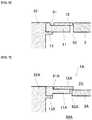
- the susceptor ring 7is composed of two members in order to further prevent the decrease in the film thickness distribution and the film quality. This point will be described.
- the susceptor ring 7is intended to function as a preheat ring.
- a first ring 11 configuring the susceptor ring 7is spaced apart with respect to the outer periphery of the susceptor, and a step portion 91 having a low upper surface is formed on the inner peripheral side of the first ring.
- a second ring 12is mounted on the step portion 91.
- the second ring 12faces the spacing portion 92 formed between the first ring 11 and the susceptor 3, that is, the second ring 12 is provided so as to protrude toward the spacing portion 92.
- the second ring 12is provided so that the upper surface thereof may have the same height as the upper surface of the susceptor 3.
- the reaction gas which is maintained in a state to be mixed and rectified by the reaction gas supply passage 41 and the likecan be smoothly supplied to the substrate W so as not to reduce the speed as much as possible.
- the upper surface of the susceptor 3here refers to an upper surface of a region where no recess 3a (refer to FIG. 1 ) for a substrate of the susceptor 3 is formed.
- the second ring 12 of the present embodimentemploys silicon carbide as a material in view of the thermal conductivity.
- the susceptor ring 7can be configured more accurately by configuring the second ring 12 and the first ring 11 as separate members in this manner. That is, it is possible to bring the distance between the susceptor ring 7 and the susceptor 3 close to a lower limit, and thereby the wraparound of the reaction gas to the back surface side of the substrate W, that is, to the reaction chamber lower portion 64 can be reduced and the temperature distribution of the substrate can be equalized.
- the distribution of the film thickness and the distribution of the film quality of the formed filmare equalized.
- the heat transfer between the first ring 11 and the second ring 12can be suppressed by making the first ring 11 and the second ring 12 as two members more than in the case of making the first ring 11 and the second ring 12 as one member.
- the second ring 12is formed to be thinner than the first ring 11. Thereby, it is possible to suppress the radiation heat loss from the susceptor 3. Furthermore, since the second ring 12 is thin, it is possible to reduce the amount of heat required for maintaining (preheating) the second ring 12 in a predetermined high temperature.
- the first ring 11when the first ring 11 is made of a material having a low thermal conductivity, the first ring 11 functions as a heat insulating material, and it is possible to further enhance the above effect.
- the second ring 12is configured so as to face the spacing portion 92 in the present embodiment, but it is not limited thereto. At least if the second ring 12 is configured to be mounted on the step portion 91 of the first ring 11, it is possible to configure the susceptor ring 7 accurately. So the distance between the susceptor ring 7 and the susceptor 3 can be brought close to a lower limit. Thereby, the wraparound of the reaction gas to the back surface side of the substrate W can be reduced and the temperature distribution of the substrate can be equalized.
- the ceiling surface of the ceiling plate 21is also likely to be coated with the reaction gas. If the ceiling surface is coated, the ceiling surface is fogged and the film deposition may not be performed sufficiently, by the cold-wall-type epitaxial apparatus, to be heated from the heating means 23 through the ceiling plate 21.
- the present embodimentby providing the grooves 75 on the wall surface of the reaction gas supply passage 41 and configuring the susceptor ring 7 with two members as described above, the reaction gas is hardly retained in the reaction chamber, and as a result, the adhesion of the coating material can be suppressed. Thereby, it is possible to perform sufficient and multiple film deposition steps in succession.
- FIG. 7Another embodiment of the present invention will be described with reference to FIG. 7 .
- the second ring 12Ais provided so as to cover the spacing portion 92A, which is different from Embodiment 1.
- the first ring 11Ais also mounted on the flange portion 13A of the sidewall portion 32A.
- the second ring 12Ais mounted on the step portion 91A of the first ring 11A and the inner peripheral side thereof faces the outer periphery of the susceptor 3A.
- the second ring 12Ais provided so as to cover the spacing portion 92A, it is possible to further prevent the reaction gas flowing into the reaction chamber 2A from entering into the reaction chamber lower portion 64A.
- the amount of the overlap between the second ring 12A and the susceptor 3Ais preferably small.
- the thickness of the second ring 12A in such present embodimentis about 0.8 mm. By using such a thickness, heat loss by radiation from the susceptor 3A to the second ring 12A can be suppressed as much as possible.
- the epitaxial growth apparatus 1A(the distance H between the substrate surface and the ceiling plate 21 is 9.27 mm), an epitaxial growth is performed on the basis of the following growth conditions.
- An epitaxial growthis performed in the same conditions as in Working Example 1 except for changing the first source gas flow rate to 13.5 SLM.
- An epitaxial growthis performed in the same conditions as in Working Example 1 except for changing the first source gas flow rate to 17.0 SLM.
- An epitaxial growthis performed by a conventional epitaxial growth apparatus (the distance H between the substrate surface and the ceiling plate 21 is 20 mm, no grooves 75 are provided, and the susceptor ring consists of one member) on the basis of the same growth conditions as in Working Example 1 except for the second source gas flow rate of 34.0 SLM and the rotation speed of 35.0 RPM.
- An epitaxial growthis performed by a conventional epitaxial growth apparatus (the distance H between the substrate surface and the ceiling plate 21 is 20 mm, no grooves 75 are provided, and the susceptor ring consists of one member) on the basis of the same growth conditions as in Working Example 2 except for the second source gas flow rate of 34.0 SLM and the rotation speed of 35.0 RPM.
- An epitaxial growthis performed by a conventional epitaxial growth apparatus (the distance H between the substrate surface and the ceiling plate 21 is 20 mm, no grooves 75 are provided, and the susceptor ring consists of one member) on the basis of the same growth conditions as in Working Example 3 except for the second source gas flow rate of 34.0 SLM and the rotation speed of 35.0 RPM.
- the growth rate of the film according to each of Working Examples and Comparative Exampleswas detected.
- the relation between the detected growth rate and the first source gasis shown in FIG. 8 .
- the growth ratewas improved by more than 50 %.
Landscapes
- Chemical & Material Sciences (AREA)
- Engineering & Computer Science (AREA)
- Materials Engineering (AREA)
- Metallurgy (AREA)
- Organic Chemistry (AREA)
- Chemical Kinetics & Catalysis (AREA)
- General Chemical & Material Sciences (AREA)
- Mechanical Engineering (AREA)
- Crystallography & Structural Chemistry (AREA)
- Physics & Mathematics (AREA)
- Condensed Matter Physics & Semiconductors (AREA)
- General Physics & Mathematics (AREA)
- Manufacturing & Machinery (AREA)
- Computer Hardware Design (AREA)
- Microelectronics & Electronic Packaging (AREA)
- Power Engineering (AREA)
- Health & Medical Sciences (AREA)
- Toxicology (AREA)
- Chemical Vapour Deposition (AREA)
Description
- The present invention relates to an epitaxial growth apparatus.
- Conventionally, an epitaxial growth apparatus for growing an epitaxial film on the substrate by epitaxial growth is known (for example, refer to Patent Literature 1). The apparatus comprises a processing chamber; a rotatable substrate support disposed in the processing chamber and configured to rotate a substrate around a rotational axis. A reaction gas is introduced parallel to a horizontal direction of the substrate to be deposited on the substrate on the substrate support.
US 2007/0281084 A1 describes a layer depositing reactor for forming an epitaxial layer.JP 2005 307238 A JP 2007 324286 A JP 2006 049503 A JP 2004 063779 A - PTL 1: Japanese Patent Application Publication No.
2001 - 520456 - For such an epitaxial growth apparatus, it is now required to increase the growth rate. In this case, it is not preferable to include a large amount of a first source gas in a reaction gas in order to increase the growth rate, for example, because the deposition cost increases and particles increase.
- Therefore, an object of the present invention is to solve the problems in the prior art described above, and is intended to provide an epitaxial growth apparatus with an improved growth rate.
- An epitaxial growth apparatus of the present invention comprises: a reaction chamber defined by a substrate mounting portion on which a substrate is mounted, a ceiling plate with optical transparency and a sidewall portion; a heating means which is mounted outside said reaction chamber and heats the substrate mounted in said reaction chamber through said ceiling plate; and a reaction gas introducing means which introduces a reaction gas parallel to a horizontal direction of the substrate into said reaction chamber, characterized in that a distance between a center of said ceiling plate and the substrate mounted on said substrate mounting portion is configured to be less than 10 mm. In the present invention, the distance between the center of the ceiling plate and the substrate is less than 10 mm, and thereby, it is possible to suppress the spread of the boundary layer when a reaction gas is introduced into the reaction chamber to improve the growth rate.
- The epitaxial growth apparatus further includes a susceptor ring provided in an outer periphery of the substrate mounting portion. The susceptor ring consists of a first ring portion provided to be spaced apart with respect to an outer periphery of the substrate mounting portion and a second ring portion provided in an inner peripheral side of said first ring portion and placed in an opened recess.
- It is preferable that said ceiling plate is fixed to an annular support portion in which through-holes are formed in a top view; and the through-holes in said support portion have diameters gradually reduced toward said substrate side and said ceiling plate is fixed to an edge portion on the substrate side. By making the support portion in such a shape, the ceiling plate can be supported so that the distance between the center of the ceiling plate and the substrate may be less than 10 mm even in a condition with a high thermal stress.
- It is preferable that a supply passage which supplies a reaction gas into said reaction chamber is formed in said sidewall portion; and said supply passage has a wall portion where the reaction gas introduced from said reaction gas introducing means collides and rectifying grooves along a flow direction of the reaction gas are provided in at least both edge portions of said wall portion. By providing the rectifying grooves, it is possible to improve the linearity of the reaction gas which decreases when the distance between the center of the ceiling plate and the substrate is less than 10 mm.
- It is preferable that said rectifying grooves are provided so as to face respective holes which are arrayed in a row in the longitudinal direction of the rectifying plate facing said supply passage in a side opposite to said wall portion. By being provided in this way, it is possible to enhance the rectification property.
- It is preferable that the arrayed holes are formed for each of a plurality of regions in said rectifying plate and said rectifying grooves are provided corresponding to the holes in regions located at both edges of said regions. By being provided in this way, it is possible to enhance the rectification property.
- It is preferable that said rectifying grooves are provided so as to have centers of the grooves face the center of the annular sidewall portion. By being provided in this way, it is possible to enhance the rectification property.
- It is preferable that a susceptor ring is provided in an outer periphery of said substrate mounting portion; and the susceptor ring consists of a first ring portion which is spaced apart in the outer periphery of the susceptor; and a second ring portion provided in an inner peripheral side of said first ring portion and placed in an opened recess. By being composed of two members in this way, it is possible to reduce the amount of heat loss.
- It is preferable that said second ring portion is provided to face a spacing portion between said susceptor and said first ring portion, so as to suppress the wraparound of the reaction gas.
- It is preferable that said second ring portion is provided to cover a spacing portion between said susceptor and said first ring portion, so as to further suppress the wraparound of the reaction gas.
- The epitaxial growth apparatus of the present invention can exhibit an excellent effect of improving the growth rate.
FIG. 1 is a cross-sectional view showing the whole epitaxial growth apparatus.FIG. 2 is a partially exploded perspective view of an epitaxial growth apparatus for describing a reaction chamber.FIG. 3 is a partial perspective view of an epitaxial growth apparatus for describing a sidewall portion.FIG. 4 is a partial sectional view of an epitaxial growth apparatus for describing a supply passage.FIG. 5 is a schematic diagram of an epitaxial growth apparatus for describing a supply passage.FIG. 6 is a partial sectional view of an epitaxial growth apparatus for describing a pre-heat ring.FIG. 7 is a partial sectional view of an epitaxial growth apparatus according to Embodiment 2..FIG. 8 is a graph showing the results of Working Examples and Comparative Examples.- The epitaxial growth apparatus according to
Embodiment 1 of the present invention will be described with reference toFIGS.1 and2 . - The
epitaxial growth apparatus 1 is a film deposition apparatus for epitaxially growing a film such as silicon and the like on a substrate W. - The
epitaxial growth apparatus 1 has areaction chamber 2. Thereaction chamber 2 is composed of asusceptor 3 for mounting the substrate W thereon, asidewall portion 4 and aceiling portion 5. - The
susceptor 3 is a circular plate-like member in a top view, and is configured to be slightly larger than the substrate W. Thesusceptor 3 is provided with a recess 3a for a substrate for mounting a substrate W thereon. Thesusceptor 3 is supported by asusceptor support portion 6 having a plurality of arms. Thesusceptor support portion 6 moves up and down from a deposition position P1 where a film deposition is performed on a substrate W to a substrate transfer position P2 where a substrate W is loaded to and unloaded from theepitaxial growth apparatus 1 while supporting thesusceptor 3. Thesusceptor support portion 6 is configured to rotate at the film deposition position P1 to allow the substrate W to be rotated at the film deposition position. In addition, thesusceptor support portion 6 is configured so that each arm has a thickness which is thinner than the normal thickness. Thereby, the heat from a heating means 62 to be described later is prevented from being blocked by thesusceptor support portion 6, it is possible to decrease the difference of the radiant heat of thesusceptor 3 by thesusceptor support portion 6, and it is possible to reduce the amount of heat which would otherwise escape from thesusceptor 3 to thesusceptor support portion 6. Therefore, it is possible to equalize the temperature distribution of thesusceptor 3. - The
susceptor 3 is provided with anannular susceptor ring 7 to its surroundings at the film deposition position P1. Thesusceptor ring 7 consists of afirst ring 11 and asecond ring 12 mounted on thefirst ring 11, though the details will be described later. Thesusceptor ring 7 is supported by aflange portion 13 provided on thesidewall portion 4 of thereaction chamber 2. - The
ceiling portion 5 consists of aceiling plate 21 and asupport portion 22 for supporting theceiling plate 21. Theceiling plate 21 is permeable, and is configured to allow the heat from the heating means 23 (for example, a halogen lamp) provided on the outside above theceiling plate 21 to pass through and heat the inside of thereaction chamber 2. That is, theepitaxial growth apparatus 1 of the present embodiment is a cold-wall-type epitaxial growth apparatus. In the present embodiment, quartz is used as theceiling plate 21. - The
support portion 22 for supporting the ceiling plate is annular. A through-hole 24 of thesupport portion 22 has a diameter which is gradually reduced toward the substrate side. The ceiling plate is fixed to an end portion on the substrate side of the through-hole. The fixing method includes welding. In addition, seeing thesupport portion 22 from the back surface side (lower surface side), the inner peripheral portion projects to define a projectingportion 25. The projectingportion 25 is also formed so as to have a diameter which is gradually reduced toward the projecting direction. Thus, the support portion is composed of two slope portions. - The
sidewall portion 4 consists of an annularupper sidewall portion 31 and an annularlower sidewall portion 32. The inner peripheral side of the lower sidewall portion is provided with theflange portion 13 described above. Asubstrate transfer port 30 is provided on the lower side of theflange portion 13. - The
upper sidewall portion 31 has a slope portion on the upper surface thereof corresponding to the projectingportion 25 of thesupport portion 22 described above. By having this slope surface, theupper sidewall portion 31 and thesupport portion 22 are fitted to each other. - The upper surface of the
lower sidewall portion 32 is notched in a part of the outer peripheral portion, and the region where no notch is provided is configured as a mounting surface 33 on which the upper sidewall portion is mounted. By notching the lower sidewall portion, afirst recess 34 is formed in the lower sidewall portion. That is, thefirst recess 34 is a recess formed in a portion where the mounting surface 33 of the upper surface of the lower sidewall portion is not formed. In theupper sidewall portion 31, afirst protrusion 36 is provided at a position corresponding to thefirst recess 34 when being mounted on thelower sidewall portion 32 so as to correspond to the shape of thefirst recess 34 and form agap 35 between thefirst recess 34 and thefirst protrusion 36. In addition, thegap 35 between thefirst protrusion 36 and thefirst recess 34 functions as a reaction gas supply passage 41 (a supply passage). Details about the reactiongas supply passage 41 will be described later. - Furthermore, in the region facing the
first recess 34 of thelower sidewall portion 32, the upper surface of thelower sidewall portion 32 is notched in a part of the outer periphery thereof to form asecond recess 37. In theupper sidewall portion 31, asecond protrusion 39 is formed at a position corresponding to thesecond recess 37 when being mounted on thelower sidewall portion 32 so as to correspond to the shape of thesecond recess 37 and form agap 38 between thesecond recess 37 and thesecond protrusion 39. Agas discharge passage 42 is formed by thesecond recess 37 and thesecond protrusion 39 of theupper sidewall portion 31. - Thus, the reaction
gas supply passage 41 and thegas discharge passage 42 are opposed to each other in thereaction chamber 2, and the reaction gas flows parallel to the horizontal direction of the substrate W in thereaction chamber 2. - In addition, a
purge hole 44 through which purge gas is discharged is formed in thewall surface 43 configuring thesecond recess 37 of thelower sidewall portion 32. Thepurge hole 44 is provided below theflange portion 13. Since thepurge hole 44 is provided in thewall surface 43 which configures thesecond recess 37, thepurge hole 44 faces thegas discharge passage 42. Therefore, both of the reaction gas and the purge gas are discharged to thegas discharge passage 42. - An annular mounting table 45 is provided in the lower surface side of the
sidewall portion 4, and thesidewall portion 4 is mounted on the mounting table 45. - An annular holding
portion 51 is provided on the outer peripheral side of theceiling portion 5, thesidewall portion 4 and the mounting table 45, and the annular holdingportion 51 clamps and supports theseceiling portion 5,sidewall portion 4 and mounting table 45. The holdingportion 51 is provided with a supply-side communication passage 52 which communicates with the reactiongas supply passage 41 and a discharge-side communication passage 53 which communicates with thegas discharge passage 42, respectively. - The supply-
side communication passage 52 is provided with a reactiongas introducing portion 54. From the reactiongas introducing portion 54, a first source gas and a second source gas are introduced in the present embodiment. Note that the second source gas also functions as a carrier gas. It is also possible to use a mixture of three or more gases as a reaction gas. The reactiongas introducing portion 54 is provided with a rectifyingplate 55 so as to be perpendicular to the gas flow passage. The rectifyingplate 55 is provided with a plurality ofholes 56 in a row along the circumferential direction. By the reaction gas passing through theholes 56, the first source gas and the second source gas are mixed as well as rectified. In addition, the discharge-side communication passage 53 is provided with a gas discharge portion 57. That is, the reaction gas supply passage is provided with the reaction gas introducing portion through the supply-side communication passage. In addition, the gas discharge passage is provided with the gas discharge portion through the discharge-side communication passage. In the gas discharge passage, the flow passage is provided so as to face the center of the reaction chamber. - In addition, an
apparatus bottom portion 61 is provided in the inner peripheral side lower portion of the mounting table 45. Another heating means 62 is provided in the outside of theapparatus bottom portion 61, and it is also possible to heat the substrate from below. - In the center of the
apparatus bottom portion 61, ashaft portion 63 of thesusceptor support portion 6 is inserted and a purge gas introducing portion (not shown) through which a purge gas is introduced are provided. The purge gas is introduced from a purge gas introducing means which is not shown and is provided in the purge gas introducing portion into the reaction chamberlower portion 64 configured by thelower sidewall portion 32 and the mounting table 45. Thepurge hole 44 described above communicates with the reaction chamberlower portion 64. - A film deposition method using such an epitaxial growth apparatus of the present embodiment will be described.
- The
susceptor 3 is moved to the substrate transfer position P2. A substrate W is loaded from thesubstrate transfer port 30. Thesusceptor 3 is moved to the deposition position P1. A silicon substrate having a diameter of, for example, 200mm is used as the substrate W. Thereafter, while heated by the heating means 23 and 62, a purge gas (for example, hydrogen) is introduced from the purge gas introducing portion into the reaction chamberlower portion 64. In addition, reaction gases (for example, trichlorosilane as the first source gas, and hydrogen as the second source gas) are introduced from the reactiongas introducing portion 54 into thereaction chamber 2 through the reactiongas supply passage 41. The reaction gas forms a boundary layer on the substrate surface, and the reaction occurs in the boundary layer. Thereby, a silicon film is deposited on the substrate W. The reaction gas is discharged from thegas discharge passage 42 that faces thereaction chamber 2. In addition, the purge gas is discharged to thegas discharge passage 42 through thepurge hole 44. - According to such an epitaxial growth apparatus of the present embodiment, the distance H between the ceiling surface in the reaction chamber side of the central portion of the
ceiling plate 21 and the substrate W can be less than 10 mm due to thesupport portion 22 supporting theceiling plate 21. Thereby, theepitaxial growth apparatus 1 of the present embodiment can prevent the boundary layer formed by the reaction gas flowing between theceiling panel 21 and thesusceptor 3 from spreading in the ceiling side, and as a result, the boundary layer will be narrow. Then, since the gas speed in the boundary layer increases, as a result, the gas density is improved to enhance the reaction efficiency on the substrate surface. Thereby, the growth rate can be increased in theepitaxial growth apparatus 1. - The distance H between the
ceiling plate 21 and the substrate W is less than 10 mm. Preferably, the distance H between theceiling plate 21 and the substrate W is less than 10 mm and the distance between the surface of the deposited film on the substrate and theceiling plate 21 is set to be 1 mm or more. By adopting this range, it is possible to achieve a smooth gas stream of the reaction gas while the boundary layer is formed, which is preferable. - That is, in the
reaction chamber 2 according to the present embodiment, by setting the distance between the substrate W and theceiling plate 21 to less than ever before (conventionally, about 20 mm), the boundary layer is narrowed and the reaction efficiency on the substrate surface is enhanced. As a result, the growth rate is improved. - In the present embodiment, since the
support portion 22 has a shape in which it is difficult for the stress to concentrate, it is possible in the present embodiment to set the distance H between the substrate W and theceiling plate 21 to be short, that is, less than 10 mm. Specifically, the infrared light provided by the heating means 23 generally passes through theceiling plate 21, but theceiling plate 21 itself absorbs the radiation heat from thesusceptor 3 or the substrate W. The absorbed heat is input from theceiling plate 21 through the bonding portion of thesupport portion 22 into thesupport portion 22. In particular, in the present embodiment, since the distance H between the substrate W and theceiling plate 21 is set to a predetermined short distance, the amount of absorption of the radiation heat is high and the heat which is input to thesupport portion 22 is greater than in the conventional technology. If thesupport portion 22 has a corner portion with a substantially right angle, the stress will concentrate on the corner portion and there is a possibility of cracking and the like will occur. - Therefore, the
support portion 22 is tilted in order to set theceiling plate 21 in a lower position than ever before in the present embodiment, and such a shape is employed so that theceiling plate 21 can be supported on the substrate side without providing a corner portion where stresses tend to concentrate. - In addition, the distance H between the
ceiling plate 21 and the substrate W is set to be shorter in the present embodiment in order to narrow the boundary layer as described above. As a result, the reaction gas can easily escape to the outside of the substrate W and it may be difficult to equalize the distribution of the film thickness in a substrate. Of cource, it is preferable to prevent this. Therefore, a guide portion is provided in the reactiongas supply passage 41 in the present embodiment so as to equalize the gas stream as described below. - The guide portion provided in the reaction
gas supply passage 41 will be described in details with reference toFIGS. 3 - 5 . The reactiongas supply passage 41 formed between thefirst recess 34 of thelower sidewall portion 32 and thefirst protrusion 36 of theupper sidewall portion 31 communicates with the reaction gas introducing portion, and has afirst supply passage 71 extending in a direction that matches the introducing direction of the gas from the reaction gas introducing portion. The reactiongas supply passage 41 is further provided with asecond supply passage 72 which communicates with thefirst supply passage 71 and extends in a direction perpendicular to the introducing direction of the gas, and athird supply passage 73 which communicates with thesecond supply passage 72 and extends in a direction that matches the introducing direction of the gas. Thethird supply passage 73 is in communication with thereaction chamber 2. - The
second supply passage 72 extends in the direction perpendicular to the introducing direction of the gas as described above, and thereby the gas introduced from the reaction gas introducing portion contacts with thewall surface 74 facing the reaction gas introducing portion of thesecond supply passage 72. Thereby, the reaction gas is diffused and the mixing characteristics of the reaction gas are increased. That is, thesecond supply passage 72 serves as a mixing chamber for the reaction gas. In the present embodiment,grooves 75 extending in the vertical direction are formed in the wall surface of thesecond supply passage 72 so that the gas will not stagnate in thesecond supply passage 72 in this case. Thegrooves 75 function as a guide portion. Due to the provision of thegrooves 75, the gas diffused by contacting with thewall surface 74 of the second supply passage also easily flows into thethird supply passage 73. Furthermore, by being rectified along the grooves, the linearity of the reaction gas is improved and the spreading of the reaction gas when the reaction gas flows into thereaction chamber 2 can be suppressed. - The
grooves 75 will be described in details. Thegrooves 75 are formed as a recess having a plurality of consecutive grooves on the entire surface of thewall surface 74 of thesecond supply passage 74. As shown inFIG. 5 (2), the recessedgrooves 75 are curved in the width direction of the grooves. In the present embodiment, thegrooves 75 are arcuate in a top view. Since thegrooves 75 are curved in the width direction, the reaction gas is difficult to be diffused (easily concentrated), when the reaction gas contacts thewall surface 74, that is, the bottom of thegrooves 75, and even when the reaction gas flows into the reaction chamber, the reaction gas is less likely to be spread to the outside of the substrate. Note that when the depth of thegrooves 75 is too deep, it is possible to suppress the diffusion, but it is difficult to mix the first source gas and the second source gas in the reaction gas. Thus, in the present embodiment, the depth of thegrooves 75 is 3 mm. - In addition, each of the
grooves 75 is provided toward the center C in the plane direction of thelower sidewall portion 32. That is, thegrooves 75 are provided along the circumferential direction of thelower sidewall portion 32. By providing thegrooves 75 in this way, the rectifying property increases so that the reaction gas guided by each of thegrooves 75 is directed to the center side, and the reaction gas is prevented from being dispersed in the reaction chamber. - Furthermore, each of the
grooves 75 is provided in such a position that the center of each of the grooves in the width direction and the center of theholes 56 of the rectifyingplate 55 provided on the reaction gas introducing portion are substantially matched (corresponding). That is, in the present embodiment, the number of thegrooves 75 in thewall surface 74 and the number of theholes 56 are equal. Thereby, since the reaction gas rectified by the rectifyingplate 55 flows into each of thegrooves 75 directly, the rectifying property is further enhanced and the linearity of the reaction gas is improved. - Note that the
grooves 75 are provided on the entire surface of thewall surface 74 of thesecond supply passage 72 in the present embodiment. However, thegrooves 75 have only to be provided at least in edge portions among the wall surfaces 74 of thesecond supply passage 72. Although holes of the rectifying plate are provided by being divided into a plurality of regions, the edge portions refer to portions corresponding to extreme regions of the regions. For example, in the case shown inFIG. 5 , the rectifying plate is divided into threeregions 81, and thegrooves 75 have only to be provided corresponding to the holes in theextreme regions grooves 75 are provided in order to enhance the linearity of the reaction gas at the edge portions of the reaction gas supply passage in particular. Then, it is possible to obtain such an effect simply by forming thegrooves 75 which functions as a guide portion in this case as a recess. For example, it is not preferable to provide a rectifying member in the second supply passage separately, because problems of the reaction gas mixing property, production cost and the like will occur. So it is preferable to form thegrooves 75 as a recess as described in the present embodiment. Then, since a desired effect can be achieved by rectifying the reaction gas with thegrooves 75, it is not necessary to perform a separate control for the reaction gas introducing portion. - Furthermore, in the present embodiment, the distance between the
ceiling plate 21 and the substrate W is deceased in order to narrow the boundary layer as described above. Thus, the wraparound of the reaction gas to the lower portion of the reaction chamber occurs easily and it is difficult to equalize the temperature distribution of the substrate. As a result, the decrease in the film thickness distribution and the film quality (such as the distribution of the resistivity, the occurrence of the crystal defects, etc.) when a thick film is formed has also been considered. In the present embodiment, thesusceptor ring 7 is composed of two members in order to further prevent the decrease in the film thickness distribution and the film quality. This point will be described. - The
susceptor ring 7 is intended to function as a preheat ring. Afirst ring 11 configuring thesusceptor ring 7 is spaced apart with respect to the outer periphery of the susceptor, and astep portion 91 having a low upper surface is formed on the inner peripheral side of the first ring. Asecond ring 12 is mounted on thestep portion 91. Thesecond ring 12 faces the spacingportion 92 formed between thefirst ring 11 and thesusceptor 3, that is, thesecond ring 12 is provided so as to protrude toward the spacingportion 92. Thesecond ring 12 is provided so that the upper surface thereof may have the same height as the upper surface of thesusceptor 3. Thus, by the upper surface of thesecond ring 12 provided to have the same height as the upper surface of thesusceptor 3, the reaction gas which is maintained in a state to be mixed and rectified by the reactiongas supply passage 41 and the like can be smoothly supplied to the substrate W so as not to reduce the speed as much as possible. Note that the upper surface of thesusceptor 3 here refers to an upper surface of a region where no recess 3a (refer toFIG. 1 ) for a substrate of thesusceptor 3 is formed. Thesecond ring 12 of the present embodiment employs silicon carbide as a material in view of the thermal conductivity. - Then, the
susceptor ring 7 can be configured more accurately by configuring thesecond ring 12 and thefirst ring 11 as separate members in this manner. That is, it is possible to bring the distance between thesusceptor ring 7 and thesusceptor 3 close to a lower limit, and thereby the wraparound of the reaction gas to the back surface side of the substrate W, that is, to the reaction chamberlower portion 64 can be reduced and the temperature distribution of the substrate can be equalized. Thus, in the present embodiment, the distribution of the film thickness and the distribution of the film quality of the formed film are equalized. - In addition, the heat transfer between the
first ring 11 and thesecond ring 12 can be suppressed by making thefirst ring 11 and thesecond ring 12 as two members more than in the case of making thefirst ring 11 and thesecond ring 12 as one member. - Furthermore, leakage of the reaction gas downward from between the
susceptor ring 7 and thesusceptor 3 during the film deposition can be reduced and the flow of the reaction gas is hardly disturbed by thesecond ring 12 configured to face the spacingportion 92 in this manner. In addition, since the downward leakage of the reaction gas can be reduced, it is possible to reduce the amount of particles. - In this case, the
second ring 12 is formed to be thinner than thefirst ring 11. Thereby, it is possible to suppress the radiation heat loss from thesusceptor 3. Furthermore, since thesecond ring 12 is thin, it is possible to reduce the amount of heat required for maintaining (preheating) thesecond ring 12 in a predetermined high temperature. In addition to the present embodiment, when thefirst ring 11 is made of a material having a low thermal conductivity, thefirst ring 11 functions as a heat insulating material, and it is possible to further enhance the above effect. - Note that the
second ring 12 is configured so as to face the spacingportion 92 in the present embodiment, but it is not limited thereto. At least if thesecond ring 12 is configured to be mounted on thestep portion 91 of thefirst ring 11, it is possible to configure thesusceptor ring 7 accurately. So the distance between thesusceptor ring 7 and thesusceptor 3 can be brought close to a lower limit. Thereby, the wraparound of the reaction gas to the back surface side of the substrate W can be reduced and the temperature distribution of the substrate can be equalized. - In addition, since the distance between the
ceiling plate 21 and the substrate W is decreased in order to narrow the boundary layer in the present embodiment, the ceiling surface of theceiling plate 21 is also likely to be coated with the reaction gas. If the ceiling surface is coated, the ceiling surface is fogged and the film deposition may not be performed sufficiently, by the cold-wall-type epitaxial apparatus, to be heated from the heating means 23 through theceiling plate 21. In contrast, in the present embodiment, by providing thegrooves 75 on the wall surface of the reactiongas supply passage 41 and configuring thesusceptor ring 7 with two members as described above, the reaction gas is hardly retained in the reaction chamber, and as a result, the adhesion of the coating material can be suppressed. Thereby, it is possible to perform sufficient and multiple film deposition steps in succession. - Another embodiment of the present invention will be described with reference to
FIG. 7 . - In the
epitaxial growth apparatus 1A according to the present embodiment, thesecond ring 12A is provided so as to cover thespacing portion 92A, which is different fromEmbodiment 1. In the present embodiment, thefirst ring 11A is also mounted on theflange portion 13A of thesidewall portion 32A. Thesecond ring 12A is mounted on thestep portion 91A of thefirst ring 11A and the inner peripheral side thereof faces the outer periphery of thesusceptor 3A. - In the present embodiment, since the
second ring 12A is provided so as to cover thespacing portion 92A, it is possible to further prevent the reaction gas flowing into thereaction chamber 2A from entering into the reaction chamberlower portion 64A. In order to prevent thesecond ring 12A from blocking the heating of thesusceptor 3A from a heating means not shown inFIG. 7 , the amount of the overlap between thesecond ring 12A and thesusceptor 3A is preferably small. - The thickness of the
second ring 12A in such present embodiment is about 0.8 mm. By using such a thickness, heat loss by radiation from thesusceptor 3A to thesecond ring 12A can be suppressed as much as possible. - Hereinafter, the details of the invention will be described by way of working examples.
- By the
epitaxial growth apparatus 1A (the distance H between the substrate surface and theceiling plate 21 is 9.27 mm), an epitaxial growth is performed on the basis of the following growth conditions. - First source gas (trichlorosilane) flow rate 8.5 SLM
- Second source gas (hydrogen) flow rate 80.0 SLM
- Purge gas (hydrogen) flow rate 15.0 SLM
- Growth time 600.0 seconds
- Growth temperature 1100.0 °C
- Rotation speed 20.0 RPM
- An epitaxial growth is performed in the same conditions as in Working Example 1 except for changing the first source gas flow rate to 13.5 SLM.
- An epitaxial growth is performed in the same conditions as in Working Example 1 except for changing the first source gas flow rate to 17.0 SLM.
- An epitaxial growth is performed by a conventional epitaxial growth apparatus (the distance H between the substrate surface and the
ceiling plate 21 is 20 mm, nogrooves 75 are provided, and the susceptor ring consists of one member) on the basis of the same growth conditions as in Working Example 1 except for the second source gas flow rate of 34.0 SLM and the rotation speed of 35.0 RPM. - An epitaxial growth is performed by a conventional epitaxial growth apparatus (the distance H between the substrate surface and the
ceiling plate 21 is 20 mm, nogrooves 75 are provided, and the susceptor ring consists of one member) on the basis of the same growth conditions as in Working Example 2 except for the second source gas flow rate of 34.0 SLM and the rotation speed of 35.0 RPM. - An epitaxial growth is performed by a conventional epitaxial growth apparatus (the distance H between the substrate surface and the
ceiling plate 21 is 20 mm, nogrooves 75 are provided, and the susceptor ring consists of one member) on the basis of the same growth conditions as in Working Example 3 except for the second source gas flow rate of 34.0 SLM and the rotation speed of 35.0 RPM. - The growth rate of the film according to each of Working Examples and Comparative Examples was detected. The relation between the detected growth rate and the first source gas is shown in
FIG. 8 . - As shown in
FIG. 8 , according to theepitaxial growth apparatus 1A, the growth rate was improved by more than 50 %. The more the first source gas amount was, the more the growth rate was improved. Therefore, the growth rate was improved by using the epitaxial growth apparatus of the present embodiment. - 1
- Epitaxial growth apparatus
- 2
- Reaction chamber
- 3
- Susceptor
- 4
- Sidewall portion
- 5
- Ceiling portion
- 6
- Susceptor support portion
- 7
- Susceptor ring
- 11
- First ring
- 12
- Second ring
- 13
- Flange portion
- 21
- Ceiling plate
- 22
- Support portion
- 23
- Heating means
- 24
- Through-hole
- 25
- Projecting portion
- 30
- Substrate unloading port
- 31
- Upper sidewall portion
- 32
- Lower sidewall portion
- 33
- Mounting surface
- 34
- First recess
- 35
- Gap
- 36
- First protrusion
- 37
- Second recess
- 38
- Gap
- 39
- Second protrusion
- 41
- Reaction gas supply passage
- 42
- Gas discharge passage
- 43
- Wall surface
- 44
- Purge hole
- 45
- Mounting table
- 51
- Holding portion
- 52
- Supply-side communication passage
- 53
- Discharge-side communication passage
- 54
- Reaction gas introducing portion
- 55
- Rectifying plate
- 56
- Hole
- 57
- Gas discharge portion
- 61
- Apparatus bottom portion
- 62
- Heating means
- 63
- Shaft
- 64
- Reaction chamber lower portion
- 71
- First supply passage
- 72
- Second supply passage
- 73
- Third supply passage
- 74
- Wall surface
- 75
- Groove
- 81, 82, 83
- Region
- 91
- Step portion
- 92
- Spacing portion
- W
- Substrate
Claims (8)
- An epitaxial growth apparatus, comprising:a reaction chamber (2) defined by a substrate mounting portion (3) on which a substrate (W) is mounted, a ceiling plate (21) with optical transparency and a sidewall portion (4);a heating means (23) which is mounted outside said reaction chamber and heats the substrate mounted in said reaction chamber through said ceiling plate; anda reaction gas introducing means which introduces a reaction gas parallel to a horizontal direction of the substrate into said reaction chamber,characterized in that:a distance (H) between a center of said ceiling plate and the substrate mounted on said substrate mounting portion is configured to be less than 10 mm; anda susceptor ring (7) is provided in an outer periphery of said substrate mounting portion; andthe susceptor ring consists of: a first ring portion (11) provided to be spaced apart with respect to an outer periphery of the substrate mounting portion; and a second ring portion (12) provided in an inner peripheral side of said first ring portion and placed in an opened recess.
- The epitaxial growth apparatus of claim 1,characterized in that
said ceiling plate is fixed to an annular support portion (22) in which through-holes are formed in a top view; and
the through-holes in said support portion have diameters gradually reduced toward said substrate side and said ceiling plate is fixed to an edge portion on the substrate side. - The epitaxial growth apparatus of claim 1 or 2,characterized in that
a supply passage (41) which supplies a reaction gas into said reaction chamber is formed in said sidewall portion; and
said supply passage has a wall portion where the reaction gas introduced from said reaction gas introducing means collides and rectifying grooves (75) along a flowing direction of the reaction gas are provided in at least both edge portions of said wall portion. - The epitaxial growth apparatus of claim 3,characterized in that
said rectifying grooves are provided so as to face respective holes which are arrayed in a row in the longitudinal direction of the rectifying plate (55) facing said supply passage in a side opposite to said wall portion. - The epitaxial growth apparatus of claim 3,characterized in that
holes which are arrayed are formed for each of a plurality of regions in said rectifying plate and said rectifying grooves are provided corresponding to the holes in regions located at both edges of said regions. - The epitaxial growth apparatus of any of claims 3 - 5,characterized in that
said rectifying grooves are provided so as to have centers of the grooves face the center of the annular sidewall portion. - The epitaxial growth apparatus of claim 1,characterized in that
said second ring portion is provided to face a spacing portion between said substrate mounting portion and said first ring portion. - The epitaxial growth apparatus of claim 7,characterized in that
said second ring portion is provided to cover a spacing portion between said substrate mounting portion and said first ring portion.
Priority Applications (1)
| Application Number | Priority Date | Filing Date | Title |
|---|---|---|---|
| EP18196541.9AEP3456860A3 (en) | 2012-10-26 | 2013-10-28 | Epitaxial growth apparatus |
Applications Claiming Priority (2)
| Application Number | Priority Date | Filing Date | Title |
|---|---|---|---|
| JP2012237109AJP5343162B1 (en) | 2012-10-26 | 2012-10-26 | Epitaxial growth equipment |
| PCT/JP2013/079126WO2014065428A1 (en) | 2012-10-26 | 2013-10-28 | Epitaxial growth apparatus |
Related Child Applications (1)
| Application Number | Title | Priority Date | Filing Date |
|---|---|---|---|
| EP18196541.9ADivisionEP3456860A3 (en) | 2012-10-26 | 2013-10-28 | Epitaxial growth apparatus |
Publications (3)
| Publication Number | Publication Date |
|---|---|
| EP2913844A1 EP2913844A1 (en) | 2015-09-02 |
| EP2913844A4 EP2913844A4 (en) | 2016-07-13 |
| EP2913844B1true EP2913844B1 (en) | 2018-09-26 |
Family
ID=49679220
Family Applications (2)
| Application Number | Title | Priority Date | Filing Date |
|---|---|---|---|
| EP18196541.9AWithdrawnEP3456860A3 (en) | 2012-10-26 | 2013-10-28 | Epitaxial growth apparatus |
| EP13848894.5AActiveEP2913844B1 (en) | 2012-10-26 | 2013-10-28 | Epitaxial growth apparatus |
Family Applications Before (1)
| Application Number | Title | Priority Date | Filing Date |
|---|---|---|---|
| EP18196541.9AWithdrawnEP3456860A3 (en) | 2012-10-26 | 2013-10-28 | Epitaxial growth apparatus |
Country Status (7)
| Country | Link |
|---|---|
| US (1) | US10443129B2 (en) |
| EP (2) | EP3456860A3 (en) |
| JP (1) | JP5343162B1 (en) |
| KR (3) | KR102155162B1 (en) |
| CN (2) | CN108728823B (en) |
| SG (2) | SG10201703435SA (en) |
| WO (1) | WO2014065428A1 (en) |
Families Citing this family (20)
| Publication number | Priority date | Publication date | Assignee | Title |
|---|---|---|---|---|
| JP5602903B2 (en)* | 2013-03-14 | 2014-10-08 | アプライド マテリアルズ インコーポレイテッド | Epitaxial film formation method and epitaxial growth apparatus |
| US10047457B2 (en)* | 2013-09-16 | 2018-08-14 | Applied Materials, Inc. | EPI pre-heat ring |
| WO2016154052A1 (en)* | 2015-03-25 | 2016-09-29 | Applied Materials, Inc. | Chamber components for epitaxial growth apparatus |
| WO2016191448A1 (en)* | 2015-05-27 | 2016-12-01 | Applied Materials, Inc. | Heat shield ring for high growth rate epi chamber |
| KR102184067B1 (en)* | 2017-12-27 | 2020-11-27 | 도쿄엘렉트론가부시키가이샤 | Etching method and etching apparatus |
| JP6998839B2 (en)* | 2018-06-25 | 2022-01-18 | グローバルウェーハズ・ジャパン株式会社 | Manufacturing method of epitaxial silicon wafer |
| JP7159986B2 (en)* | 2019-06-27 | 2022-10-25 | 株式会社Sumco | Epitaxial growth apparatus and epitaxial wafer manufacturing method |
| US11032945B2 (en)* | 2019-07-12 | 2021-06-08 | Applied Materials, Inc. | Heat shield assembly for an epitaxy chamber |
| JP2021068871A (en)* | 2019-10-28 | 2021-04-30 | 株式会社Sumco | Epitaxial growth device and method of manufacturing epitaxial wafer |
| CN111850514B (en)* | 2020-06-30 | 2022-11-22 | 北京北方华创微电子装备有限公司 | Air intake and exhaust component for epitaxial growth equipment and epitaxial growth equipment |
| CN111748792B (en)* | 2020-07-10 | 2022-10-21 | 北京北方华创微电子装备有限公司 | Vapor deposition apparatus |
| JP7549871B2 (en)* | 2020-10-12 | 2024-09-12 | エピクルー株式会社 | Vapor phase growth apparatus and epitaxial wafer manufacturing method |
| CN114457321B (en)* | 2022-01-21 | 2023-03-28 | 深圳市纳设智能装备有限公司 | Air inlet device and CVD equipment |
| JP7595947B2 (en) | 2022-04-28 | 2024-12-09 | エピクルー株式会社 | Parameter determination device, parameter determination method, and parameter determination program for epitaxial growth apparatus |
| CN115064471B (en)* | 2022-08-01 | 2023-11-28 | 北京屹唐半导体科技股份有限公司 | Wafer heat treatment device |
| CN115305458B (en)* | 2022-10-10 | 2023-02-03 | 中微半导体设备(上海)股份有限公司 | Gas distribution part, gas conveying device and film processing device thereof |
| KR102572438B1 (en)* | 2022-11-17 | 2023-08-30 | 주식회사 피제이피테크 | Epitaxial growth apparatus and gas supply control module used therefor |
| CN115595552B (en)* | 2022-12-16 | 2023-04-11 | 新美光(苏州)半导体科技有限公司 | Silicon carbide ring for plasma etching equipment and forming process of silicon carbide ring |
| US20240274463A1 (en)* | 2023-02-10 | 2024-08-15 | Applied Materials, Inc. | Overlapping substrate supports and pre-heat rings, and related process kits, processing chambers, methods, and components |
| US20240337537A1 (en)* | 2023-04-10 | 2024-10-10 | Applied Materials, Inc. | Systems, apparatus, and methods for monitoring plate temperature for semiconductor manufacturing |
Family Cites Families (34)
| Publication number | Priority date | Publication date | Assignee | Title |
|---|---|---|---|---|
| JPS5976875A (en)* | 1982-10-22 | 1984-05-02 | Hitachi Ltd | Magnetron type sputtering device |
| US5024716A (en)* | 1988-01-20 | 1991-06-18 | Canon Kabushiki Kaisha | Plasma processing apparatus for etching, ashing and film-formation |
| JPH02252234A (en)* | 1989-03-27 | 1990-10-11 | Toshiba Corp | Optical CVD equipment |
| JP3038524B2 (en)* | 1993-04-19 | 2000-05-08 | コマツ電子金属株式会社 | Semiconductor manufacturing equipment |
| US6500734B2 (en)* | 1993-07-30 | 2002-12-31 | Applied Materials, Inc. | Gas inlets for wafer processing chamber |
| JP3911518B2 (en)* | 1995-03-31 | 2007-05-09 | 株式会社Sumco | Susceptor for vapor phase growth apparatus and vapor phase growth method |
| US5846332A (en)* | 1996-07-12 | 1998-12-08 | Applied Materials, Inc. | Thermally floating pedestal collar in a chemical vapor deposition chamber |
| US6063440A (en)* | 1997-07-11 | 2000-05-16 | Applied Materials, Inc. | Method for aligning a wafer |
| US6099648A (en)* | 1997-08-06 | 2000-08-08 | Applied Materials, Inc. | Domed wafer reactor vessel window with reduced stress at atmospheric and above atmospheric pressures |
| TW429271B (en)* | 1997-10-10 | 2001-04-11 | Applied Materials Inc | Introducing process fluid over rotating substrates |
| US6143079A (en)* | 1998-11-19 | 2000-11-07 | Asm America, Inc. | Compact process chamber for improved process uniformity |
| JP3758579B2 (en) | 2002-01-23 | 2006-03-22 | 信越半導体株式会社 | Heat treatment apparatus and heat treatment method |
| JP3908112B2 (en) | 2002-07-29 | 2007-04-25 | Sumco Techxiv株式会社 | Susceptor, epitaxial wafer manufacturing apparatus and epitaxial wafer manufacturing method |
| US7118781B1 (en)* | 2003-04-16 | 2006-10-10 | Cree, Inc. | Methods for controlling formation of deposits in a deposition system and deposition methods including the same |
| JP2007511902A (en)* | 2003-10-29 | 2007-05-10 | エーエスエム アメリカ インコーポレイテッド | Reactor for thin film growth |
| JP5124760B2 (en)* | 2004-04-19 | 2013-01-23 | 静雄 藤田 | Film forming method and film forming apparatus |
| JP2005353775A (en)* | 2004-06-09 | 2005-12-22 | Sumco Corp | Epitaxial device |
| JP4378699B2 (en)* | 2004-08-03 | 2009-12-09 | 株式会社Sumco | Epitaxial growth equipment |
| DE602006004457D1 (en)* | 2005-07-27 | 2009-02-05 | Ingenia Technology Ltd | SIGNATURE FOR ACCESS TOKENS |
| JP4704894B2 (en)* | 2005-11-16 | 2011-06-22 | 国立大学法人京都大学 | Film forming method and film forming apparatus |
| JP5069424B2 (en)* | 2006-05-31 | 2012-11-07 | Sumco Techxiv株式会社 | Film forming reaction apparatus and method |
| TW200809926A (en)* | 2006-05-31 | 2008-02-16 | Sumco Techxiv Corp | Apparatus and method for depositing layer on substrate |
| JP2008028357A (en)* | 2006-07-24 | 2008-02-07 | Hynix Semiconductor Inc | Semiconductor device and manufacturing method thereof |
| US20080179289A1 (en)* | 2007-01-30 | 2008-07-31 | Collins Kenneth S | Process for wafer backside polymer removal with a plasma stream |
| US7954866B2 (en)* | 2008-07-03 | 2011-06-07 | Honda Motor Co., Ltd. | Bumper beam with gussets to prevent underride |
| DE102008034260B4 (en)* | 2008-07-16 | 2014-06-26 | Siltronic Ag | Method for depositing a layer on a semiconductor wafer by means of CVD in a chamber and chamber for depositing a layer on a semiconductor wafer by means of CVD |
| JP2010034474A (en)* | 2008-07-31 | 2010-02-12 | Sumco Corp | Epitaxial growth device and method of manufacturing epitaxial wafer |
| JP2010040590A (en)* | 2008-07-31 | 2010-02-18 | Sumco Corp | Epitaxial silicon wafer and method of manufacturing the same |
| JP2010050130A (en)* | 2008-08-19 | 2010-03-04 | Sumco Techxiv株式会社 | Device for supporting semiconductor wafer |
| KR102124441B1 (en)* | 2009-12-31 | 2020-06-18 | 어플라이드 머티어리얼스, 인코포레이티드 | Shadow ring for modifying wafer edge and bevel deposition |
| SG183511A1 (en)* | 2010-03-03 | 2012-09-27 | Veeco Instr Inc | Wafer carrier with sloped edge |
| JP2012146697A (en)* | 2011-01-06 | 2012-08-02 | Shin Etsu Handotai Co Ltd | Manufacturing apparatus and manufacturing method of epitaxial wafer |
| JP5837178B2 (en)* | 2011-03-22 | 2015-12-24 | アプライド マテリアルズ インコーポレイテッドApplied Materials,Incorporated | Liner assembly for chemical vapor deposition chambers |
| JP5386046B1 (en)* | 2013-03-27 | 2014-01-15 | エピクルー株式会社 | Susceptor support and epitaxial growth apparatus provided with this susceptor support |
- 2012
- 2012-10-26JPJP2012237109Apatent/JP5343162B1/enactiveActive
- 2013
- 2013-02-07USUS13/762,176patent/US10443129B2/enactiveActive
- 2013-10-28CNCN201810343931.XApatent/CN108728823B/enactiveActive
- 2013-10-28KRKR1020157012864Apatent/KR102155162B1/enactiveActive
- 2013-10-28WOPCT/JP2013/079126patent/WO2014065428A1/enactiveApplication Filing
- 2013-10-28EPEP18196541.9Apatent/EP3456860A3/ennot_activeWithdrawn
- 2013-10-28SGSG10201703435SApatent/SG10201703435SA/enunknown
- 2013-10-28KRKR1020217028138Apatent/KR102457101B1/enactiveActive
- 2013-10-28EPEP13848894.5Apatent/EP2913844B1/enactiveActive
- 2013-10-28SGSG11201502959PApatent/SG11201502959PA/enunknown
- 2013-10-28KRKR1020207025651Apatent/KR102300579B1/enactiveActive
- 2013-10-28CNCN201380054803.9Apatent/CN105103276B/enactiveActive
Non-Patent Citations (1)
| Title |
|---|
| None* |
Also Published As
| Publication number | Publication date |
|---|---|
| KR102300579B1 (en) | 2021-09-08 |
| CN108728823B (en) | 2020-09-15 |
| JP2014086688A (en) | 2014-05-12 |
| CN105103276B (en) | 2018-05-18 |
| EP3456860A3 (en) | 2019-05-08 |
| KR102457101B1 (en) | 2022-10-19 |
| EP2913844A1 (en) | 2015-09-02 |
| KR20210111361A (en) | 2021-09-10 |
| US10443129B2 (en) | 2019-10-15 |
| CN105103276A (en) | 2015-11-25 |
| SG11201502959PA (en) | 2015-05-28 |
| JP5343162B1 (en) | 2013-11-13 |
| CN108728823A (en) | 2018-11-02 |
| US20140116340A1 (en) | 2014-05-01 |
| KR20150074072A (en) | 2015-07-01 |
| WO2014065428A1 (en) | 2014-05-01 |
| SG10201703435SA (en) | 2017-05-30 |
| KR20200106564A (en) | 2020-09-14 |
| EP2913844A4 (en) | 2016-07-13 |
| KR102155162B1 (en) | 2020-09-21 |
| EP3456860A2 (en) | 2019-03-20 |
Similar Documents
| Publication | Publication Date | Title |
|---|---|---|
| EP2913844B1 (en) | Epitaxial growth apparatus | |
| JP7136945B2 (en) | Chamber components for epitaxial growth equipment | |
| JP5602903B2 (en) | Epitaxial film formation method and epitaxial growth apparatus | |
| JP5386046B1 (en) | Susceptor support and epitaxial growth apparatus provided with this susceptor support | |
| TWI754765B (en) | Inject assembly for epitaxial deposition processes | |
| JP2017224850A (en) | Deposition method by epitaxial growth and epitaxial growth apparatus | |
| JP6309252B2 (en) | Epitaxial film formation method and epitaxial growth apparatus | |
| JP6198584B2 (en) | Epitaxial film formation method and epitaxial growth apparatus | |
| JP7209675B2 (en) | Film formation method by epitaxial growth and epitaxial growth apparatus | |
| JP2018125545A (en) | Deposition method by epitaxial growth, and epitaxial growth device |
Legal Events
| Date | Code | Title | Description |
|---|---|---|---|
| PUAI | Public reference made under article 153(3) epc to a published international application that has entered the european phase | Free format text:ORIGINAL CODE: 0009012 | |
| 17P | Request for examination filed | Effective date:20150511 | |
| AK | Designated contracting states | Kind code of ref document:A1 Designated state(s):AL AT BE BG CH CY CZ DE DK EE ES FI FR GB GR HR HU IE IS IT LI LT LU LV MC MK MT NL NO PL PT RO RS SE SI SK SM TR | |
| AX | Request for extension of the european patent | Extension state:BA ME | |
| DAX | Request for extension of the european patent (deleted) | ||
| REG | Reference to a national code | Ref country code:DE Ref legal event code:R079 Ref document number:602013044293 Country of ref document:DE Free format text:PREVIOUS MAIN CLASS: H01L0021310000 Ipc:C23C0016455000 | |
| RA4 | Supplementary search report drawn up and despatched (corrected) | Effective date:20160614 | |
| RIC1 | Information provided on ipc code assigned before grant | Ipc:C30B 29/06 20060101ALI20160608BHEP Ipc:C23C 16/458 20060101ALI20160608BHEP Ipc:C23C 16/48 20060101ALI20160608BHEP Ipc:C23C 16/455 20060101AFI20160608BHEP Ipc:C30B 25/14 20060101ALI20160608BHEP | |
| 17Q | First examination report despatched | Effective date:20170905 | |
| GRAP | Despatch of communication of intention to grant a patent | Free format text:ORIGINAL CODE: EPIDOSNIGR1 | |
| INTG | Intention to grant announced | Effective date:20180418 | |
| GRAS | Grant fee paid | Free format text:ORIGINAL CODE: EPIDOSNIGR3 | |
| GRAA | (expected) grant | Free format text:ORIGINAL CODE: 0009210 | |
| AK | Designated contracting states | Kind code of ref document:B1 Designated state(s):AL AT BE BG CH CY CZ DE DK EE ES FI FR GB GR HR HU IE IS IT LI LT LU LV MC MK MT NL NO PL PT RO RS SE SI SK SM TR | |
| REG | Reference to a national code | Ref country code:GB Ref legal event code:FG4D | |
| REG | Reference to a national code | Ref country code:CH Ref legal event code:EP | |
| REG | Reference to a national code | Ref country code:AT Ref legal event code:REF Ref document number:1046134 Country of ref document:AT Kind code of ref document:T Effective date:20181015 | |
| REG | Reference to a national code | Ref country code:IE Ref legal event code:FG4D | |
| REG | Reference to a national code | Ref country code:DE Ref legal event code:R096 Ref document number:602013044293 Country of ref document:DE | |
| RAP2 | Party data changed (patent owner data changed or rights of a patent transferred) | Owner name:APPLIED MATERIALS, INC. | |
| REG | Reference to a national code | Ref country code:NL Ref legal event code:MP Effective date:20180926 | |
| PG25 | Lapsed in a contracting state [announced via postgrant information from national office to epo] | Ref country code:RS Free format text:LAPSE BECAUSE OF FAILURE TO SUBMIT A TRANSLATION OF THE DESCRIPTION OR TO PAY THE FEE WITHIN THE PRESCRIBED TIME-LIMIT Effective date:20180926 Ref country code:FI Free format text:LAPSE BECAUSE OF FAILURE TO SUBMIT A TRANSLATION OF THE DESCRIPTION OR TO PAY THE FEE WITHIN THE PRESCRIBED TIME-LIMIT Effective date:20180926 Ref country code:LT Free format text:LAPSE BECAUSE OF FAILURE TO SUBMIT A TRANSLATION OF THE DESCRIPTION OR TO PAY THE FEE WITHIN THE PRESCRIBED TIME-LIMIT Effective date:20180926 Ref country code:SE Free format text:LAPSE BECAUSE OF FAILURE TO SUBMIT A TRANSLATION OF THE DESCRIPTION OR TO PAY THE FEE WITHIN THE PRESCRIBED TIME-LIMIT Effective date:20180926 Ref country code:BG Free format text:LAPSE BECAUSE OF FAILURE TO SUBMIT A TRANSLATION OF THE DESCRIPTION OR TO PAY THE FEE WITHIN THE PRESCRIBED TIME-LIMIT Effective date:20181226 Ref country code:GR Free format text:LAPSE BECAUSE OF FAILURE TO SUBMIT A TRANSLATION OF THE DESCRIPTION OR TO PAY THE FEE WITHIN THE PRESCRIBED TIME-LIMIT Effective date:20181227 Ref country code:NO Free format text:LAPSE BECAUSE OF FAILURE TO SUBMIT A TRANSLATION OF THE DESCRIPTION OR TO PAY THE FEE WITHIN THE PRESCRIBED TIME-LIMIT Effective date:20181226 | |
| REG | Reference to a national code | Ref country code:LT Ref legal event code:MG4D | |
| PG25 | Lapsed in a contracting state [announced via postgrant information from national office to epo] | Ref country code:HR Free format text:LAPSE BECAUSE OF FAILURE TO SUBMIT A TRANSLATION OF THE DESCRIPTION OR TO PAY THE FEE WITHIN THE PRESCRIBED TIME-LIMIT Effective date:20180926 Ref country code:AL Free format text:LAPSE BECAUSE OF FAILURE TO SUBMIT A TRANSLATION OF THE DESCRIPTION OR TO PAY THE FEE WITHIN THE PRESCRIBED TIME-LIMIT Effective date:20180926 Ref country code:LV Free format text:LAPSE BECAUSE OF FAILURE TO SUBMIT A TRANSLATION OF THE DESCRIPTION OR TO PAY THE FEE WITHIN THE PRESCRIBED TIME-LIMIT Effective date:20180926 | |
| REG | Reference to a national code | Ref country code:AT Ref legal event code:MK05 Ref document number:1046134 Country of ref document:AT Kind code of ref document:T Effective date:20180926 | |
| PG25 | Lapsed in a contracting state [announced via postgrant information from national office to epo] | Ref country code:CZ Free format text:LAPSE BECAUSE OF FAILURE TO SUBMIT A TRANSLATION OF THE DESCRIPTION OR TO PAY THE FEE WITHIN THE PRESCRIBED TIME-LIMIT Effective date:20180926 Ref country code:ES Free format text:LAPSE BECAUSE OF FAILURE TO SUBMIT A TRANSLATION OF THE DESCRIPTION OR TO PAY THE FEE WITHIN THE PRESCRIBED TIME-LIMIT Effective date:20180926 Ref country code:IT Free format text:LAPSE BECAUSE OF FAILURE TO SUBMIT A TRANSLATION OF THE DESCRIPTION OR TO PAY THE FEE WITHIN THE PRESCRIBED TIME-LIMIT Effective date:20180926 Ref country code:RO Free format text:LAPSE BECAUSE OF FAILURE TO SUBMIT A TRANSLATION OF THE DESCRIPTION OR TO PAY THE FEE WITHIN THE PRESCRIBED TIME-LIMIT Effective date:20180926 Ref country code:AT Free format text:LAPSE BECAUSE OF FAILURE TO SUBMIT A TRANSLATION OF THE DESCRIPTION OR TO PAY THE FEE WITHIN THE PRESCRIBED TIME-LIMIT Effective date:20180926 Ref country code:EE Free format text:LAPSE BECAUSE OF FAILURE TO SUBMIT A TRANSLATION OF THE DESCRIPTION OR TO PAY THE FEE WITHIN THE PRESCRIBED TIME-LIMIT Effective date:20180926 Ref country code:PL Free format text:LAPSE BECAUSE OF FAILURE TO SUBMIT A TRANSLATION OF THE DESCRIPTION OR TO PAY THE FEE WITHIN THE PRESCRIBED TIME-LIMIT Effective date:20180926 Ref country code:NL Free format text:LAPSE BECAUSE OF FAILURE TO SUBMIT A TRANSLATION OF THE DESCRIPTION OR TO PAY THE FEE WITHIN THE PRESCRIBED TIME-LIMIT Effective date:20180926 Ref country code:IS Free format text:LAPSE BECAUSE OF FAILURE TO SUBMIT A TRANSLATION OF THE DESCRIPTION OR TO PAY THE FEE WITHIN THE PRESCRIBED TIME-LIMIT Effective date:20190126 | |
| PG25 | Lapsed in a contracting state [announced via postgrant information from national office to epo] | Ref country code:PT Free format text:LAPSE BECAUSE OF FAILURE TO SUBMIT A TRANSLATION OF THE DESCRIPTION OR TO PAY THE FEE WITHIN THE PRESCRIBED TIME-LIMIT Effective date:20190126 Ref country code:SK Free format text:LAPSE BECAUSE OF FAILURE TO SUBMIT A TRANSLATION OF THE DESCRIPTION OR TO PAY THE FEE WITHIN THE PRESCRIBED TIME-LIMIT Effective date:20180926 Ref country code:SM Free format text:LAPSE BECAUSE OF FAILURE TO SUBMIT A TRANSLATION OF THE DESCRIPTION OR TO PAY THE FEE WITHIN THE PRESCRIBED TIME-LIMIT Effective date:20180926 | |
| REG | Reference to a national code | Ref country code:CH Ref legal event code:PL | |
| REG | Reference to a national code | Ref country code:BE Ref legal event code:MM Effective date:20181031 | |
| REG | Reference to a national code | Ref country code:DE Ref legal event code:R097 Ref document number:602013044293 Country of ref document:DE | |
| PG25 | Lapsed in a contracting state [announced via postgrant information from national office to epo] | Ref country code:LU Free format text:LAPSE BECAUSE OF NON-PAYMENT OF DUE FEES Effective date:20181028 | |
| REG | Reference to a national code | Ref country code:IE Ref legal event code:MM4A | |
| PG25 | Lapsed in a contracting state [announced via postgrant information from national office to epo] | Ref country code:MC Free format text:LAPSE BECAUSE OF FAILURE TO SUBMIT A TRANSLATION OF THE DESCRIPTION OR TO PAY THE FEE WITHIN THE PRESCRIBED TIME-LIMIT Effective date:20180926 Ref country code:DK Free format text:LAPSE BECAUSE OF FAILURE TO SUBMIT A TRANSLATION OF THE DESCRIPTION OR TO PAY THE FEE WITHIN THE PRESCRIBED TIME-LIMIT Effective date:20180926 | |
| PLBE | No opposition filed within time limit | Free format text:ORIGINAL CODE: 0009261 | |
| STAA | Information on the status of an ep patent application or granted ep patent | Free format text:STATUS: NO OPPOSITION FILED WITHIN TIME LIMIT | |
| GBPC | Gb: european patent ceased through non-payment of renewal fee | Effective date:20181226 | |
| PG25 | Lapsed in a contracting state [announced via postgrant information from national office to epo] | Ref country code:CH Free format text:LAPSE BECAUSE OF NON-PAYMENT OF DUE FEES Effective date:20181031 Ref country code:LI Free format text:LAPSE BECAUSE OF NON-PAYMENT OF DUE FEES Effective date:20181031 Ref country code:BE Free format text:LAPSE BECAUSE OF NON-PAYMENT OF DUE FEES Effective date:20181031 | |
| 26N | No opposition filed | Effective date:20190627 | |
| PG25 | Lapsed in a contracting state [announced via postgrant information from national office to epo] | Ref country code:FR Free format text:LAPSE BECAUSE OF NON-PAYMENT OF DUE FEES Effective date:20181126 Ref country code:IE Free format text:LAPSE BECAUSE OF NON-PAYMENT OF DUE FEES Effective date:20181028 Ref country code:SI Free format text:LAPSE BECAUSE OF FAILURE TO SUBMIT A TRANSLATION OF THE DESCRIPTION OR TO PAY THE FEE WITHIN THE PRESCRIBED TIME-LIMIT Effective date:20180926 | |
| PG25 | Lapsed in a contracting state [announced via postgrant information from national office to epo] | Ref country code:GB Free format text:LAPSE BECAUSE OF NON-PAYMENT OF DUE FEES Effective date:20181226 | |
| PG25 | Lapsed in a contracting state [announced via postgrant information from national office to epo] | Ref country code:MT Free format text:LAPSE BECAUSE OF NON-PAYMENT OF DUE FEES Effective date:20181028 | |
| PG25 | Lapsed in a contracting state [announced via postgrant information from national office to epo] | Ref country code:TR Free format text:LAPSE BECAUSE OF FAILURE TO SUBMIT A TRANSLATION OF THE DESCRIPTION OR TO PAY THE FEE WITHIN THE PRESCRIBED TIME-LIMIT Effective date:20180926 | |
| PG25 | Lapsed in a contracting state [announced via postgrant information from national office to epo] | Ref country code:MK Free format text:LAPSE BECAUSE OF NON-PAYMENT OF DUE FEES Effective date:20180926 Ref country code:HU Free format text:LAPSE BECAUSE OF FAILURE TO SUBMIT A TRANSLATION OF THE DESCRIPTION OR TO PAY THE FEE WITHIN THE PRESCRIBED TIME-LIMIT; INVALID AB INITIO Effective date:20131028 Ref country code:CY Free format text:LAPSE BECAUSE OF FAILURE TO SUBMIT A TRANSLATION OF THE DESCRIPTION OR TO PAY THE FEE WITHIN THE PRESCRIBED TIME-LIMIT Effective date:20180926 | |
| PGFP | Annual fee paid to national office [announced via postgrant information from national office to epo] | Ref country code:DE Payment date:20240919 Year of fee payment:12 |