EP2902888B1 - Touch panel calibration system - Google Patents
Touch panel calibration systemDownload PDFInfo
- Publication number
- EP2902888B1 EP2902888B1EP14153766.2AEP14153766AEP2902888B1EP 2902888 B1EP2902888 B1EP 2902888B1EP 14153766 AEP14153766 AEP 14153766AEP 2902888 B1EP2902888 B1EP 2902888B1
- Authority
- EP
- European Patent Office
- Prior art keywords
- capacitance
- capacitive
- readout integrated
- stage
- integrated circuit
- Prior art date
- Legal status (The legal status is an assumption and is not a legal conclusion. Google has not performed a legal analysis and makes no representation as to the accuracy of the status listed.)
- Active
Links
Images


Classifications
- G—PHYSICS
- G06—COMPUTING OR CALCULATING; COUNTING
- G06F—ELECTRIC DIGITAL DATA PROCESSING
- G06F3/00—Input arrangements for transferring data to be processed into a form capable of being handled by the computer; Output arrangements for transferring data from processing unit to output unit, e.g. interface arrangements
- G06F3/01—Input arrangements or combined input and output arrangements for interaction between user and computer
- G06F3/03—Arrangements for converting the position or the displacement of a member into a coded form
- G06F3/041—Digitisers, e.g. for touch screens or touch pads, characterised by the transducing means
- G06F3/0416—Control or interface arrangements specially adapted for digitisers
- G06F3/0418—Control or interface arrangements specially adapted for digitisers for error correction or compensation, e.g. based on parallax, calibration or alignment
- G—PHYSICS
- G01—MEASURING; TESTING
- G01R—MEASURING ELECTRIC VARIABLES; MEASURING MAGNETIC VARIABLES
- G01R35/00—Testing or calibrating of apparatus covered by the other groups of this subclass
- G01R35/005—Calibrating; Standards or reference devices, e.g. voltage or resistance standards, "golden" references
- G—PHYSICS
- G06—COMPUTING OR CALCULATING; COUNTING
- G06F—ELECTRIC DIGITAL DATA PROCESSING
- G06F3/00—Input arrangements for transferring data to be processed into a form capable of being handled by the computer; Output arrangements for transferring data from processing unit to output unit, e.g. interface arrangements
- G06F3/01—Input arrangements or combined input and output arrangements for interaction between user and computer
- G06F3/03—Arrangements for converting the position or the displacement of a member into a coded form
- G06F3/041—Digitisers, e.g. for touch screens or touch pads, characterised by the transducing means
- G06F3/044—Digitisers, e.g. for touch screens or touch pads, characterised by the transducing means by capacitive means
- G06F3/0443—Digitisers, e.g. for touch screens or touch pads, characterised by the transducing means by capacitive means using a single layer of sensing electrodes
Definitions
- the present inventionconcerns, among others, capacitive detection of conductive bodies in proximity to an electrode or to an array of electrodes, such as used in capacitive touch screens.
- the capacitor to detectis created between one electrode and a finger or pen approaching thereto, such that the second electrode may be considered as referred to ground.
- Capacitive sensor arrayssuch as those in capacitive touchscreens are ubiquitous in today's human-to-device interaction. As depicted in figures 1a and 1b , such devices can be grouped into two main divisions:
- US 2012256868 A1discloses a capacitive touch sensor with two input terminals; US 2011012618 A1 a capacity-to-digital converter with a switchable calibration capacitor; US 2012256869 A1 a readout for a differential capacitive sense array on a chip, US 2011018558 A1 a calibration mechanism including the insertion of one or two reference capacitors on measurement lines connected to the corners of a touch sensor; US 2009066674 A1 discloses circuits for measuring floating and ground-referenced capacitances. All these five documents comprise means for device calibration.
- This inventionproposes new systems and methods to test and calibrate capacitive sensor array systems. Compared to prior art, the new system and methods offer the following advantages:
- Figure 1represents a known capacitive touch panel 120 comprising a rectangular regular grid of capacitive sensors 125.
- the gridcomprises eight rows of four sensors although the number of sensors in most concrete realizations would be considerably higher.
- the sensors 125are inserted between the row lines 132 and the column lines 135 that are connected to the sensing circuit 160 and respectively to the modulation source 90.
- the proximity of a conductive object 60is detected by a variation (in general a decrease) of the capacity of the nearby sensors.
- FIG. 1billustrates a possible realization of a single-ended capacitive sensor.
- the capacitive sensorsare individual pixels 128 that are not matrix-addressed, as in the previous example, but individually connected to the sensing circuit 161 by the connection lines 139.
- the capacitive pixels 128are biased at a fixed voltage with respect to a common reference conductor, that can be regarded as a floating ground reference, and which is driven by the modulation source 90, such that the capacitance sensing circuit can read the capacity between each of the capacitive 'pixels' 128 and a neighbouring conductive body 60, for example a finger. Since it can be assumed that the body 60 is grounded, or at a fixed potential with respect to the ground, its approach is indicated by an increase of the capacitance to ground of the nearby pixels 128.
- FIG. 3represents schematically an aspect of the detection principle.
- the sense pixels 128are deposited on a suitable substrate 43, possibly a transparent substrate that has the sense pixels 128 on one face, and the guard electrode 120 on the other, as represented, and that is placed above the LCD display 40.
- the sense pixels 128are individually connected, by the sense lines 193, to the input terminals of the respective CDC 168, which are here represented by a possible realization of the analogue input stage only, for simplicity.
- the CDC 168are referred to the potential of the guard electrode 120, and their input terminals are at the same potential as the guard electrode, or maintain a constant voltage with respect thereto.
- the CDC 168have an input stage that is configured as a charge amplifier, but other dispositions are possible. Thanks to this, the readout system of the invention is relatively insensitive to the capacities 48 between the pixels 128 and the ground electrode 120, and also to the inter-pixel capacities (not represented).
- the CDC stages 168read a signal has the same shape as the modulation signal and whose amplitude is in first approximation proportional to the capacities 65 between each pixel and the nearby body 60, the ratio being determined, among others, by the values of the feedback capacitors 166 of each stage.
- An aspect of the present disclosureconcerns a capacitive touch sensitive device that includes a CDC that is arranged to measure a capacitance present to its input and deliver the measured value as a digital code.
- a concrete realization of a touch sensitive devicemay need to read a very large number of capacity sensitive electrodes in parallel, and to this end include a plurality of capacitance-to-digital stages either in a single integrated circuit or in a plurality of integrated circuits.
- the capacitance-to-digital convertercompares the value of the input capacitance with that of a reference capacitance, typically an internal capacitor on chip, by measuring the amplitude of a modulation voltage at the input terminals.
- a reference capacitancetypically an internal capacitor on chip
- C itypically varies from stage to stage within a circuit due to fabrication tolerances and mismatches, as well as from circuit to circuit. All capacitive converter stages in the same circuit may share a common V ref , but this reference value may vary from a circuit to another. Finally, V mod is common to the system.
- TFCDC transfer function
- Figure 2illustrates an ideal transfer function 321 in which the code output code (y axis) follows the equation 1, as well as a real transfer function 323 that is affected by offset and slope errors and deviates from the ideal behaviour. Even if it is not represented in the figure, the real transfer function may also include integral and differential nonlinearities and other higher order errors.
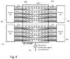
- FIG. 4illustrates schematically a possible structure of a capacitive touch panel.
- a sensitive surface 120is covered with a matrix of capacitive sensors 128, each comprising an electrode that constitutes a tiny capacitor together with a common guard electrode 130.
- the capacitance of the individual sensorsis read by one or several circuits 161, 162, 163, 164, each of which is connected to a group of electrodes.
- the guard electrodeis preferably connected to a source of variable voltage 90 that allows measuring the capacity of the individual electrodes 128.
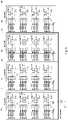
- Figure 5shows a readout apparatus connectable to a capacitive touch panel, wherein the apparatus comprises several capacitive readout integrated circuits 161, 162, 163, 164, each of which includes a plurality of CDC 168 as capacitance-measuring units arranged to provide a signal representative of a capacity of electrodes on the capacitive touch panel, that are connected by the signal lines CSi,xy etc. and the multiplexers 165.
- the readout apparatushas at least one reference capacitor that is selectively connectable to either input of the CDCs 168.
- each of the circuitshas a calibration mode in which the CDCs input are connected in turn to the reference capacitor.
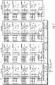
- the inventionincludes features that allow equalizing, compensating, or correcting the differences of CDC transfer functions between stages, at the IC level or between different IC at the system level.
- the function that need be equalized between stagesis 1 C i ⁇ V mod V ref .
- the inventionincludes one or several on-chip test capacitor Cref 173 and preferably switching means 185, 186 arranged to measure the CDC response for each stage, thus allowing channel equalization as a part of the overall circuit calibration.
- the on-chip test capacitors 173are variable devices whose capacitance can be selectively changed, for example by a digital control signal. This feature enables measuring of the response of the CDC stages 161 for two or more values of the input capacitance.
- Such variable capacitorscan be realized by switched banks of fixed capacitors, or any other suitable way.
- the calibrationcan be carried out against internal capacitors 173 inside the circuits, or also, if required, against an external reference capacitor 177 connected on common reference capacitance lines.
- FIG. 8represents a variant that allows the measure of floating/mutual capacitor.
- the circuitincludes a stimulation mode selector unit 193 that changes the capacitor testing method according to the logical value present at its 'stim_mode' input: in a normal mode, selectable by setting the 'stim_mode' to the 0 value, the VG terminal, connected to the guard electrode 130 of the touch panel is driven by the AC modulation source 90, and the cr_b line that is connected to the reference capacitors Cref1 and Cref,ext is tied to ground potential; in a floating measure mode, selectable by setting the 'stim_mode' input to the '1' value, the VG terminal is set to ground, and the AC modulation signal is instead applied to the cr_b line that sets the reference voltage capacitors Cref1 and Cref,ext.
- the circuitinclude a polarity inversion stage 197 that is applied to the AC control signal in the floating measure mode, such that the polarity of the signal measured by the CDC stages remains
- the arrangement of figure 8allows switching around the guard stimulation signal to move the reference point, actually emulating a mutual capacitance sensing.
- this measureis insensitive to parasitic capacitances.
- an automatic capacitance calibration with one integrated circuitmay proceed as follows:
- a capacitance calibration using on-chip reference capacitorsmay develop as follows:
- the circuit of figure 6also allows an absolute capacitance calibration by means of an external reference capacitor Cref, ext. This could be carried out for example as follows:
- the integrated circuitsmay comprise means to determine the value of the internal reference capacitors 173 by charging them with a known current and measuring the time needed to reach a given voltage. In this manner, if the circuits include or have access to precise current and voltage references, the absolute values of the internal reference capacitors 173 can be accurately measured, and an absolute calibration of the CDC stages obtained.
- the integrated circuitcould include or have access to a shared current or voltage reference whose absolute value is not precisely known.
- the integrated circuitscan however charge the reference capacitors with a stable current tied to the shared reference and, in this manner their gains can be at least equalized among the IC and stages, even if the absolute value is not precisely defined.
Landscapes
- Engineering & Computer Science (AREA)
- General Engineering & Computer Science (AREA)
- Theoretical Computer Science (AREA)
- Physics & Mathematics (AREA)
- General Physics & Mathematics (AREA)
- Human Computer Interaction (AREA)
- Measurement Of Resistance Or Impedance (AREA)
- Position Input By Displaying (AREA)
Description
- The present invention concerns, among others, capacitive detection of conductive bodies in proximity to an electrode or to an array of electrodes, such as used in capacitive touch screens. In embodiments, the capacitor to detect is created between one electrode and a finger or pen approaching thereto, such that the second electrode may be considered as referred to ground.
- Capacitive sensor arrays such as those in capacitive touchscreens are ubiquitous in today's human-to-device interaction. As depicted in
figures 1a and 1b , such devices can be grouped into two main divisions: - differential (mutual) capacitance sensing matrix
This is the technology most represented in the market. The sensor arrays typically comprise a matrix of electrodes arranged in rows and columns, and a dedicated circuitry sensing the line-to-line capacitance. The performances of these systems can be excellent when the user touches the screen (sensing of x/y coordinates) or approaches considerably, typically less than a few millimetres, the sensing array, but they degrade quickly with the increase of the distance z between the panel and finger, such that these sensors are not well suited for touch-less applications like hovering. - single-ended (self) capacitance sensing matrix
These sensors include an array of individual pixels that measure an absolute capacitance to ground. They combine an excellent performance in x, y and z, allowing for touch-less or "3D" sensing, as well as behaving better with gloved hands and styli, and offering unlimited multi-touch sensing. Compared to the previous group, these higher performances come at the expense of more complex panel and sensor routing, and associated circuitry. - To guarantee high performance i.e. to reduce errors introduced by sensor and sensing circuitry, all matrix sensors must have matched and accurate capacitance measurements. In the case of self capacitance array measurements, best performance is achieved when ensuring uniform capacitance readings among all channels/sensors (equalized channel readings) as well as absolute capacitance value measurement. Specific advanced test and calibration systems and methods must be used to reach these goals.
- Known systems typically attempt to test and calibrate a given capacitance-sensitive stage inside an integrated circuit (IC) by itself during a single IC production test, possibly against a known external reference capacitance. This operation is not trivial and does neither offer the possibility of equalizing the transfer function among different stages or different IC, nor of recalibrating or dynamically adapting the transfer function in the application or during operation.
US 2012256868 A1 discloses a capacitive touch sensor with two input terminals;US 2011012618 A1 a capacity-to-digital converter with a switchable calibration capacitor;US 2012256869 A1 a readout for a differential capacitive sense array on a chip,US 2011018558 A1 a calibration mechanism including the insertion of one or two reference capacitors on measurement lines connected to the corners of a touch sensor;US 2009066674 A1 discloses circuits for measuring floating and ground-referenced capacitances. All these five documents comprise means for device calibration. - This invention proposes new systems and methods to test and calibrate capacitive sensor array systems. Compared to prior art, the new system and methods offer the following advantages:
- inexpensive, low complexity, flexibility
- ability to measure and calibrate at different levels:
- o during integrated circuit (IC) production test; e.g. on automated test equipment (ATE)
- o in-situ on the final application system with touchscreen module
- o "on-the-fly" or dynamically during touchscreen usage; e.g. to compensate for environmental changes (e.g. temperature, user conditions)
- According to the invention, these aims are achieved by means of the object of the appended claims.
- The invention will be better understood with the aid of the description of an embodiment given by way of example and illustrated by the figures, in which:
Figures 1a and 1b shows schematically the general structure of differential and single-ended capacitive touch-sensitive devices as known in the artFigure 2 is a plot of the response functions of an ideal Capacitance-to-Digital Converter (CDC) and of a real CDC having offset and gain variations.Figure 3 illustrates schematically an aspect of the readout system.Figure 4 illustrates schematically a tactile system comprising a matrix of capacity-sensitive electrodes divided in groups, each group being read by an independent circuit.Figure 5 illustrates a possible interconnection of several circuits, each of which has a plurality of CDC stages, to read a matrix of capacity-sensitive electrodes.Figure 6 illustrates an interconnection scheme similar to that offigure 5 including a shared capacitance reference line according to the invention.Figure 7 illustrates an interconnection scheme similar to those offigures 5 and6 including a daisy-chained capacitance reference line.Figure 8 shows schematically a capacitive-sensitive circuit including additional means for measuring a floating capacitor- Some aspects of the present disclosure that are in common with another known solution will now be reviewed with reference to
figures 1a and 1b. Figure 1 represents a knowncapacitive touch panel 120 comprising a rectangular regular grid ofcapacitive sensors 125. In the illustrated example the grid comprises eight rows of four sensors although the number of sensors in most concrete realizations would be considerably higher. Thesensors 125 are inserted between therow lines 132 and thecolumn lines 135 that are connected to thesensing circuit 160 and respectively to themodulation source 90. The proximity of aconductive object 60 is detected by a variation (in general a decrease) of the capacity of the nearby sensors. Figure 1b illustrates a possible realization of a single-ended capacitive sensor. In this realization, the capacitive sensors areindividual pixels 128 that are not matrix-addressed, as in the previous example, but individually connected to thesensing circuit 161 by theconnection lines 139. Thecapacitive pixels 128 are biased at a fixed voltage with respect to a common reference conductor, that can be regarded as a floating ground reference, and which is driven by themodulation source 90, such that the capacitance sensing circuit can read the capacity between each of the capacitive 'pixels' 128 and a neighbouringconductive body 60, for example a finger. Since it can be assumed that thebody 60 is grounded, or at a fixed potential with respect to the ground, its approach is indicated by an increase of the capacitance to ground of thenearby pixels 128.Figure 3 represents schematically an aspect of the detection principle. Thesense pixels 128 are deposited on asuitable substrate 43, possibly a transparent substrate that has thesense pixels 128 on one face, and theguard electrode 120 on the other, as represented, and that is placed above theLCD display 40. Thesense pixels 128 are individually connected, by thesense lines 193, to the input terminals of the respective CDC 168, which are here represented by a possible realization of the analogue input stage only, for simplicity.- According to an important aspect, the CDC 168 are referred to the potential of the
guard electrode 120, and their input terminals are at the same potential as the guard electrode, or maintain a constant voltage with respect thereto. In the represented example, the CDC 168 have an input stage that is configured as a charge amplifier, but other dispositions are possible. Thanks to this, the readout system of the invention is relatively insensitive to thecapacities 48 between thepixels 128 and theground electrode 120, and also to the inter-pixel capacities (not represented). When the guard electrode is excited by themodulation source 90, the CDCstages 168 read a signal has the same shape as the modulation signal and whose amplitude is in first approximation proportional to thecapacities 65 between each pixel and thenearby body 60, the ratio being determined, among others, by the values of thefeedback capacitors 166 of each stage. - An aspect of the present disclosure concerns a capacitive touch sensitive device that includes a CDC that is arranged to measure a capacitance present to its input and deliver the measured value as a digital code. A concrete realization of a touch sensitive device may need to read a very large number of capacity sensitive electrodes in parallel, and to this end include a plurality of capacitance-to-digital stages either in a single integrated circuit or in a plurality of integrated circuits. The capacitance-to-digital converter compares the value of the input capacitance with that of a reference capacitance, typically an internal capacitor on chip, by measuring the amplitude of a modulation voltage at the input terminals. Formally it can be characterized by a transform function:

- k
- constant (determined for example by design)
- Cs
- input capacitance to be measured
- Ci
- internal / on chip reference capacitance
- Vmod
- modulation voltage
- Vref
- reference voltage
- Ci typically varies from stage to stage within a circuit due to fabrication tolerances and mismatches, as well as from circuit to circuit. All capacitive converter stages in the same circuit may share a commonVref, but this reference value may vary from a circuit to another. Finally,Vmod is common to the system. This leads to CDC transfer function (TF) errors, both in offset and gain, varying from stage to stage.
Figure 2 illustrates anideal transfer function 321 in which the code output code (y axis) follows theequation 1, as well as areal transfer function 323 that is affected by offset and slope errors and deviates from the ideal behaviour. Even if it is not represented in the figure, the real transfer function may also include integral and differential nonlinearities and other higher order errors. Figure 4 illustrates schematically a possible structure of a capacitive touch panel. Asensitive surface 120 is covered with a matrix ofcapacitive sensors 128, each comprising an electrode that constitutes a tiny capacitor together with acommon guard electrode 130. The capacitance of the individual sensors is read by one orseveral circuits variable voltage 90 that allows measuring the capacity of theindividual electrodes 128.Figure 5 shows a readout apparatus connectable to a capacitive touch panel, wherein the apparatus comprises several capacitive readout integratedcircuits CDC 168 as capacitance-measuring units arranged to provide a signal representative of a capacity of electrodes on the capacitive touch panel, that are connected by the signal lines CSi,xy etc. and themultiplexers 165. Importantly the readout apparatus has at least one reference capacitor that is selectively connectable to either input of theCDCs 168. Preferably, each of the circuits has a calibration mode in which the CDCs input are connected in turn to the reference capacitor.- Importantly the invention includes features that allow equalizing, compensating, or correcting the differences of CDC transfer functions between stages, at the IC level or between different IC at the system level. Mathematically, the function that need be equalized between stages is

- According to an important aspect illustrated in
figures 6 and7 , the invention includes one or several on-chiptest capacitor Cref 173 and preferably switching means 185, 186 arranged to measure the CDC response for each stage, thus allowing channel equalization as a part of the overall circuit calibration. - Preferably, the on-
chip test capacitors 173 are variable devices whose capacitance can be selectively changed, for example by a digital control signal. This feature enables measuring of the response of the CDC stages 161 for two or more values of the input capacitance. Such variable capacitors can be realized by switched banks of fixed capacitors, or any other suitable way. - Another important aspect is the presence of common
reference capacitance lines - The calibration can be carried out against
internal capacitors 173 inside the circuits, or also, if required, against anexternal reference capacitor 177 connected on common reference capacitance lines. - The variants illustrated by
figures 6 and7 differ in the way in which the common reference lines are used. In the former, a singlecommon reference line 171 is used among all circuits, while in the latter it is a daisy-chained system with sharedlines Figure 8 represents a variant that allows the measure of floating/mutual capacitor. For simplicity, only one integrated circuit is represented. The circuit includes a stimulationmode selector unit 193 that changes the capacitor testing method according to the logical value present at its 'stim_mode' input: in a normal mode, selectable by setting the 'stim_mode' to the 0 value, the VG terminal, connected to theguard electrode 130 of the touch panel is driven by theAC modulation source 90, and the cr_b line that is connected to the reference capacitors Cref1 and Cref,ext is tied to ground potential; in a floating measure mode, selectable by setting the 'stim_mode' input to the '1' value, the VG terminal is set to ground, and the AC modulation signal is instead applied to the cr_b line that sets the reference voltage capacitors Cref1 and Cref,ext. Preferably, the circuit include apolarity inversion stage 197 that is applied to the AC control signal in the floating measure mode, such that the polarity of the signal measured by the CDC stages remains the same as in the normal mode.- The arrangement of
figure 8 allows switching around the guard stimulation signal to move the reference point, actually emulating a mutual capacitance sensing. Advantageously, this measure is insensitive to parasitic capacitances. - Turning now to the circuit represented in
figure 6 , an automatic capacitance calibration with one integrated circuit may proceed as follows: - measure 1st capacitance point
- o connect internal Cref1 to stage 11 CDC; select a 1st Cref1 value, may be typically selected to be OfF capacitance
- o measure Cref1 with
CDC stage 11;store code 11 - o repeat above step for
stages
- measure 2nd capacitance point
- o connect internal Cref1 to stage 11 CDC; select a 2nd Cref1 value different from that of
measurement # 1 - o measure Cref1 with
CDC stage 11;store code 11 - o repeat above step for
stages
- o connect internal Cref1 to stage 11 CDC; select a 2nd Cref1 value different from that of
- (optionally: measure more capacitance points by changing internal Cref1 value; e.g. 3dr, 4th etc. capacitance points)
- extract all offset and relative gain errors for each stage and correct to equalize all stages; e.g. digital/software post-processing correction on the codes using simple linear regression on 2 points (or more)
- In the case of a multiple-IC implementation, a capacitance calibration using on-chip reference capacitors may develop as follows:
- measure IC 1:
- o measure 1st capacitance point
- ▪ connect internal Cref1 to stage 11 CDC (disconnect Cref,ext, unused); select a 1st Cref1 value, may be typically selected to be 0fF capacitance
- ▪ measure Cref1 with
CDC stage 11;store code 11 - ▪ repeat above step for
stages
- o measure 2nd capacitance point
- ▪ connect internal Cref1 to stage 11 CDC (disconnect Cref,ext, unused); select a 2nd Cref1 value different from that of 1st capacitance measurement
- ▪ measure Cref1 with
CDC stage 11;store code 11 - ▪ repeat above step for
stages
- ∘ optionally: measure more capacitance points by changing internal Cref1 value similarly to 1st capacitance point measurement
- ∘ optionally: perform cross-IC measurements using the other Cref2, Cref3,..,Crefz on-chip capacitors
- o measure 1st capacitance point
- repeat above measurements for IC2, IC3, ICz; each IC stage measures the same on-chip reference capacitors Cref1 from IC1 (not its own Cref2/3/.../z)
- extract all offset and gain errors for each stage and correct to equalize all stages; e.g. digital/software post-processing correction on the codes using simple linear regression on 2 points (or more)
- The circuit of
figure 6 also allows an absolute capacitance calibration by means of an external reference capacitor Cref, ext. This could be carried out for example as follows: - measure IC 1:
- o measure 1st capacitance point
- ▪ connect internal Cref1 to stage 11 CDC (disconnect Cref,ext, unused); Cref1 value may be typically selected to be 0fF capacitance
- ▪ measure Cref1 with
CDC stage 11;store code 11 - ▪ repeat above step for
stages
- o measure 2nd capacitance point
- ▪ connect external Cref,ext to stage 11 CDC (disconnect Cref1, unused)
- ▪ measure Cref,ext with
CDC stage 11;store code 11 - ▪ repeat above step for
stages
- o (optional: measure more capacitance points by changing internal Cref1 value similarly to 1st capacitance point measurement)
- o measure 1st capacitance point
- repeat above measurements for IC2, IC3, ICz; each IC stage measures the same reference capacitors, i.e. Cref1 and Cref,ext in this case
- extract all offset and gain errors for each stage and correct to equalize all stages; e.g. digital/software post-processing correction on the codes using linear regression on 2 or more points.
- In the case of daisy chained
CR lines Figure 7 , the same calibration procedures as proposed above can be used, but by selectively connecting pairs of adjacent circuits to the reference line by acting selectively on theswitches 188, calibrating the circuits in each adjacent pair with respect to each other, and finally combining the result in a global calibration using the overlaps, for example as follows: - measurement and calibration of IC1 & IC2
- measurement and calibration of IC2 & IC3
- measurement and calibration of IC3 & ICz
- combining gain/slope error corrections among IC1, IC2, IC3, ICz
- According to a possible variant the integrated circuits may comprise means to determine the value of the
internal reference capacitors 173 by charging them with a known current and measuring the time needed to reach a given voltage. In this manner, if the circuits include or have access to precise current and voltage references, the absolute values of theinternal reference capacitors 173 can be accurately measured, and an absolute calibration of the CDC stages obtained. - In a variant of the above calibration, the integrated circuit could include or have access to a shared current or voltage reference whose absolute value is not precisely known. The integrated circuits can however charge the reference capacitors with a stable current tied to the shared reference and, in this manner their gains can be at least equalized among the IC and stages, even if the absolute value is not precisely defined.


Claims (3)
- A readout apparatus connectable to a capacitive touch panel (120) comprising several capacitive readout integrated circuits (161-164), each of which includes a reference terminal and a plurality of capacitance-measuring units (168) arranged to provide a signal representative of a capacitance of electrodes (128) on the capacitive touch panel, each capacitance-measuring unit (168) comprising a multiplexer with several inputs followed by a capacitance-to-digital converter and wherein one input of each multiplexer is connected to a common conductor of the capacitive readout integrated circuit, each capacitive readout integrated circuit having a reference capacitor (173) connected through a first switch (185) of the capacitive readout integrated circuit to the common conductor, the common conductor being also connected through a second switch (186) of the capacitive readout integrated circuit to the reference terminal, wherein, in a calibration mode, the capacitive readout integrated circuits are configured such that the reference terminals of the capacitive readout integrated circuits are connected to a common reference line (171), wherein the capacitive readout integrated circuits (161-164) are arranged to sequentially connect said common reference line by their respective second switches to their respective common conductor s and to calibrate their response s, measuring the reference capacitor (173) of one and the same capacitive readout integrated circuit.
- The readout apparatus of the preceding claim, in which the reference capacitor (173) is a variable capacitor.
- The readout apparatus of any of the preceding claims, including a guard electrode (VG) connected to a modulation voltage source (90) and to a common reference electrode of the capacitive touch panel.
Priority Applications (4)
| Application Number | Priority Date | Filing Date | Title |
|---|---|---|---|
| EP14153766.2AEP2902888B1 (en) | 2014-02-04 | 2014-02-04 | Touch panel calibration system |
| US14/604,816US9766751B2 (en) | 2014-02-04 | 2015-01-26 | Touch panel calibration system |
| KR1020150016628AKR101829647B1 (en) | 2014-02-04 | 2015-02-03 | Touch panel calibration system |
| CN201510058068.XACN104834418B (en) | 2014-02-04 | 2015-02-04 | Touch panel calibration system |
Applications Claiming Priority (1)
| Application Number | Priority Date | Filing Date | Title |
|---|---|---|---|
| EP14153766.2AEP2902888B1 (en) | 2014-02-04 | 2014-02-04 | Touch panel calibration system |
Publications (2)
| Publication Number | Publication Date |
|---|---|
| EP2902888A1 EP2902888A1 (en) | 2015-08-05 |
| EP2902888B1true EP2902888B1 (en) | 2022-10-05 |
Family
ID=50064452
Family Applications (1)
| Application Number | Title | Priority Date | Filing Date |
|---|---|---|---|
| EP14153766.2AActiveEP2902888B1 (en) | 2014-02-04 | 2014-02-04 | Touch panel calibration system |
Country Status (4)
| Country | Link |
|---|---|
| US (1) | US9766751B2 (en) |
| EP (1) | EP2902888B1 (en) |
| KR (1) | KR101829647B1 (en) |
| CN (1) | CN104834418B (en) |
Families Citing this family (8)
| Publication number | Priority date | Publication date | Assignee | Title |
|---|---|---|---|---|
| EP2793007A1 (en)* | 2013-04-18 | 2014-10-22 | SIKA Dr.Siebert & Kühn GmbH & Co. KG. | Calibrator for calibration of temperature function devices |
| DE112016006605T5 (en)* | 2016-03-15 | 2018-11-22 | Olympus Corporation | Touch panel device and method for operating a touch panel device |
| US10120512B2 (en) | 2016-04-08 | 2018-11-06 | Microsoft Technology Licensing, Llc | Hover sensor |
| WO2019127313A1 (en)* | 2017-12-29 | 2019-07-04 | 深圳市汇顶科技股份有限公司 | Method for calibrating node capacitors |
| CN112997057B (en)* | 2018-09-26 | 2023-07-18 | 德克萨斯仪器股份有限公司 | Method and sensor system with integrated calibration mechanism |
| KR102302879B1 (en)* | 2019-05-22 | 2021-09-17 | 어보브반도체 주식회사 | Apparatus and method for automatically calibrating capacitance per channel |
| CN113777409B (en)* | 2021-08-19 | 2024-10-15 | 北京他山科技有限公司 | Distributed capacitive sensor system |
| CN118897125A (en)* | 2021-08-19 | 2024-11-05 | 北京他山科技有限公司 | A distributed capacitance sensor system |
Citations (1)
| Publication number | Priority date | Publication date | Assignee | Title |
|---|---|---|---|---|
| US20130063157A1 (en)* | 2010-05-07 | 2013-03-14 | Stmicroelectronics (Rousset) Sas | Method and device for characterizing or measuring a floating capacitance |
Family Cites Families (17)
| Publication number | Priority date | Publication date | Assignee | Title |
|---|---|---|---|---|
| US6977646B1 (en) | 2001-11-30 | 2005-12-20 | 3M Innovative Properties Co. | Touch screen calibration system and method |
| US8248081B2 (en)* | 2007-09-06 | 2012-08-21 | Cypress Semiconductor Corporation | Calibration of single-layer touch-sensor device |
| JP5337039B2 (en)* | 2008-04-01 | 2013-11-06 | ローム株式会社 | Electrostatic sensor |
| TWI364697B (en)* | 2008-05-30 | 2012-05-21 | Chimei Innolux Corp | Touch-sensitive liquid crystal display device and method for fabricating same |
| US8810542B2 (en) | 2008-09-10 | 2014-08-19 | Apple Inc. | Correction of parasitic capacitance effect in touch sensor panels |
| TW201013495A (en)* | 2008-09-30 | 2010-04-01 | Hannstar Display Corp | In-cell capacitive type sensing input display device |
| US8188754B2 (en)* | 2009-07-15 | 2012-05-29 | Maxim Integrated Products, Inc. | Method and apparatus for sensing capacitance value and converting it into digital format |
| KR101040925B1 (en)* | 2009-09-08 | 2011-06-17 | 한국과학기술원 | Lead-Out Circuit of Touch Screen |
| US7863966B1 (en)* | 2009-09-17 | 2011-01-04 | Himax Technologies Limited | Readout circuit for touch panel |
| US8274491B2 (en)* | 2010-06-21 | 2012-09-25 | Pixart Imaging Inc. | Capacitive touchscreen signal acquisition without panel reset |
| US8547359B2 (en)* | 2010-06-21 | 2013-10-01 | Pixart Imaging Inc. | Capacitive touchscreen system with switchable charge acquisition circuit |
| US8508493B2 (en)* | 2010-06-21 | 2013-08-13 | Pixart Imaging Inc. | Reduction of electromagnetic interference in a capacitive touchscreen system |
| KR101715850B1 (en)* | 2010-09-07 | 2017-03-13 | 엘지디스플레이 주식회사 | Readout circuit for touch sensor |
| US9268441B2 (en)* | 2011-04-05 | 2016-02-23 | Parade Technologies, Ltd. | Active integrator for a capacitive sense array |
| KR101239844B1 (en)* | 2011-04-11 | 2013-03-06 | 주식회사 동부하이텍 | apparatus for sensing a touch |
| US8395599B2 (en)* | 2011-07-15 | 2013-03-12 | Pixart Imaging, Inc. | Low voltage capacitive touchscreen charge acquisition and readout systems, circuits and methods for high system noise immunity |
| TWI457810B (en)* | 2012-01-06 | 2014-10-21 | Elan Microelectronics Corp | Method of detecting floating mode of a touch panel |
- 2014
- 2014-02-04EPEP14153766.2Apatent/EP2902888B1/enactiveActive
- 2015
- 2015-01-26USUS14/604,816patent/US9766751B2/enactiveActive
- 2015-02-03KRKR1020150016628Apatent/KR101829647B1/enactiveActive
- 2015-02-04CNCN201510058068.XApatent/CN104834418B/enactiveActive
Patent Citations (1)
| Publication number | Priority date | Publication date | Assignee | Title |
|---|---|---|---|---|
| US20130063157A1 (en)* | 2010-05-07 | 2013-03-14 | Stmicroelectronics (Rousset) Sas | Method and device for characterizing or measuring a floating capacitance |
Also Published As
| Publication number | Publication date |
|---|---|
| EP2902888A1 (en) | 2015-08-05 |
| CN104834418B (en) | 2019-11-12 |
| US9766751B2 (en) | 2017-09-19 |
| KR20150092014A (en) | 2015-08-12 |
| CN104834418A (en) | 2015-08-12 |
| KR101829647B1 (en) | 2018-02-19 |
| US20150220209A1 (en) | 2015-08-06 |
Similar Documents
| Publication | Publication Date | Title |
|---|---|---|
| EP2902888B1 (en) | Touch panel calibration system | |
| US11481066B2 (en) | Providing a baseline capacitance for a capacitance sensing channel | |
| US8866494B2 (en) | Attenuator circuit of a capacitance-sensing circuit | |
| US10146359B2 (en) | Common electrode auto-compensation method | |
| US9395850B2 (en) | Coordinate input device and display device with the same | |
| US9557853B2 (en) | Touch detecting circuit and semiconductor integrated circuit using the same | |
| US8274491B2 (en) | Capacitive touchscreen signal acquisition without panel reset | |
| US9910544B1 (en) | Uniformity correction method for low cost and non-rectangular touch sensor matrices | |
| US8432170B1 (en) | Integrated capacitance model circuit | |
| US8547359B2 (en) | Capacitive touchscreen system with switchable charge acquisition circuit | |
| US20120182252A1 (en) | Differential Capacitive Touchscreen or Touch Panel | |
| US9626048B2 (en) | Touch screen and related touch sensing control circuit | |
| US10732779B2 (en) | Touch panel including pad electrodes and a drive/readout circuit, and touch display including same | |
| US20170293376A1 (en) | Hover sensor | |
| CN103324366A (en) | Capacitor detection device and capacitive touch system applying same | |
| US20190114018A1 (en) | Active Matrix Touch Panel With Narrow Bezel | |
| KR20180034335A (en) | Panel driving apparatus and panel driving method | |
| TWI645326B (en) | Resistive force sensing circuit and resistive force sensing apparatus | |
| KR20110081474A (en) | High precision single layer touch screen device and positioning method | |
| KR20140003099A (en) | Touch display apparatus | |
| KR101585917B1 (en) | Hybrid scan type touch detecting method and apparatus in flexible touch screen panel | |
| RU2602744C2 (en) | Use of method of measuring rlc parameters according to patent ru 2100813 in devices with touch panel or screen | |
| US9830016B2 (en) | Touch display panel, touch display device and touch detection method | |
| Tortosa et al. | A crosstalk error correction algorithm for Capacitive Sensor panels |
Legal Events
| Date | Code | Title | Description |
|---|---|---|---|
| PUAI | Public reference made under article 153(3) epc to a published international application that has entered the european phase | Free format text:ORIGINAL CODE: 0009012 | |
| 17P | Request for examination filed | Effective date:20140204 | |
| AK | Designated contracting states | Kind code of ref document:A1 Designated state(s):AL AT BE BG CH CY CZ DE DK EE ES FI FR GB GR HR HU IE IS IT LI LT LU LV MC MK MT NL NO PL PT RO RS SE SI SK SM TR | |
| AX | Request for extension of the european patent | Extension state:BA ME | |
| 17P | Request for examination filed | Effective date:20160106 | |
| RBV | Designated contracting states (corrected) | Designated state(s):AL AT BE BG CH CY CZ DE DK EE ES FI FR GB GR HR HU IE IS IT LI LT LU LV MC MK MT NL NO PL PT RO RS SE SI SK SM TR | |
| STAA | Information on the status of an ep patent application or granted ep patent | Free format text:STATUS: EXAMINATION IS IN PROGRESS | |
| 17Q | First examination report despatched | Effective date:20190808 | |
| GRAP | Despatch of communication of intention to grant a patent | Free format text:ORIGINAL CODE: EPIDOSNIGR1 | |
| STAA | Information on the status of an ep patent application or granted ep patent | Free format text:STATUS: GRANT OF PATENT IS INTENDED | |
| INTG | Intention to grant announced | Effective date:20220523 | |
| GRAS | Grant fee paid | Free format text:ORIGINAL CODE: EPIDOSNIGR3 | |
| GRAA | (expected) grant | Free format text:ORIGINAL CODE: 0009210 | |
| STAA | Information on the status of an ep patent application or granted ep patent | Free format text:STATUS: THE PATENT HAS BEEN GRANTED | |
| AK | Designated contracting states | Kind code of ref document:B1 Designated state(s):AL AT BE BG CH CY CZ DE DK EE ES FI FR GB GR HR HU IE IS IT LI LT LU LV MC MK MT NL NO PL PT RO RS SE SI SK SM TR | |
| REG | Reference to a national code | Ref country code:GB Ref legal event code:FG4D | |
| REG | Reference to a national code | Ref country code:CH Ref legal event code:EP | |
| REG | Reference to a national code | Ref country code:AT Ref legal event code:REF Ref document number:1523153 Country of ref document:AT Kind code of ref document:T Effective date:20221015 | |
| REG | Reference to a national code | Ref country code:IE Ref legal event code:FG4D | |
| REG | Reference to a national code | Ref country code:DE Ref legal event code:R096 Ref document number:602014085120 Country of ref document:DE | |
| REG | Reference to a national code | Ref country code:LT Ref legal event code:MG9D | |
| REG | Reference to a national code | Ref country code:NL Ref legal event code:MP Effective date:20221005 | |
| REG | Reference to a national code | Ref country code:AT Ref legal event code:MK05 Ref document number:1523153 Country of ref document:AT Kind code of ref document:T Effective date:20221005 | |
| PG25 | Lapsed in a contracting state [announced via postgrant information from national office to epo] | Ref country code:NL Free format text:LAPSE BECAUSE OF FAILURE TO SUBMIT A TRANSLATION OF THE DESCRIPTION OR TO PAY THE FEE WITHIN THE PRESCRIBED TIME-LIMIT Effective date:20221005 | |
| PG25 | Lapsed in a contracting state [announced via postgrant information from national office to epo] | Ref country code:SE Free format text:LAPSE BECAUSE OF FAILURE TO SUBMIT A TRANSLATION OF THE DESCRIPTION OR TO PAY THE FEE WITHIN THE PRESCRIBED TIME-LIMIT Effective date:20221005 Ref country code:PT Free format text:LAPSE BECAUSE OF FAILURE TO SUBMIT A TRANSLATION OF THE DESCRIPTION OR TO PAY THE FEE WITHIN THE PRESCRIBED TIME-LIMIT Effective date:20230206 Ref country code:NO Free format text:LAPSE BECAUSE OF FAILURE TO SUBMIT A TRANSLATION OF THE DESCRIPTION OR TO PAY THE FEE WITHIN THE PRESCRIBED TIME-LIMIT Effective date:20230105 Ref country code:LT Free format text:LAPSE BECAUSE OF FAILURE TO SUBMIT A TRANSLATION OF THE DESCRIPTION OR TO PAY THE FEE WITHIN THE PRESCRIBED TIME-LIMIT Effective date:20221005 Ref country code:FI Free format text:LAPSE BECAUSE OF FAILURE TO SUBMIT A TRANSLATION OF THE DESCRIPTION OR TO PAY THE FEE WITHIN THE PRESCRIBED TIME-LIMIT Effective date:20221005 Ref country code:ES Free format text:LAPSE BECAUSE OF FAILURE TO SUBMIT A TRANSLATION OF THE DESCRIPTION OR TO PAY THE FEE WITHIN THE PRESCRIBED TIME-LIMIT Effective date:20221005 Ref country code:AT Free format text:LAPSE BECAUSE OF FAILURE TO SUBMIT A TRANSLATION OF THE DESCRIPTION OR TO PAY THE FEE WITHIN THE PRESCRIBED TIME-LIMIT Effective date:20221005 | |
| PG25 | Lapsed in a contracting state [announced via postgrant information from national office to epo] | Ref country code:RS Free format text:LAPSE BECAUSE OF FAILURE TO SUBMIT A TRANSLATION OF THE DESCRIPTION OR TO PAY THE FEE WITHIN THE PRESCRIBED TIME-LIMIT Effective date:20221005 Ref country code:PL Free format text:LAPSE BECAUSE OF FAILURE TO SUBMIT A TRANSLATION OF THE DESCRIPTION OR TO PAY THE FEE WITHIN THE PRESCRIBED TIME-LIMIT Effective date:20221005 Ref country code:LV Free format text:LAPSE BECAUSE OF FAILURE TO SUBMIT A TRANSLATION OF THE DESCRIPTION OR TO PAY THE FEE WITHIN THE PRESCRIBED TIME-LIMIT Effective date:20221005 Ref country code:IS Free format text:LAPSE BECAUSE OF FAILURE TO SUBMIT A TRANSLATION OF THE DESCRIPTION OR TO PAY THE FEE WITHIN THE PRESCRIBED TIME-LIMIT Effective date:20230205 Ref country code:HR Free format text:LAPSE BECAUSE OF FAILURE TO SUBMIT A TRANSLATION OF THE DESCRIPTION OR TO PAY THE FEE WITHIN THE PRESCRIBED TIME-LIMIT Effective date:20221005 Ref country code:GR Free format text:LAPSE BECAUSE OF FAILURE TO SUBMIT A TRANSLATION OF THE DESCRIPTION OR TO PAY THE FEE WITHIN THE PRESCRIBED TIME-LIMIT Effective date:20230106 | |
| REG | Reference to a national code | Ref country code:DE Ref legal event code:R097 Ref document number:602014085120 Country of ref document:DE | |
| P01 | Opt-out of the competence of the unified patent court (upc) registered | Effective date:20230530 | |
| PG25 | Lapsed in a contracting state [announced via postgrant information from national office to epo] | Ref country code:SM Free format text:LAPSE BECAUSE OF FAILURE TO SUBMIT A TRANSLATION OF THE DESCRIPTION OR TO PAY THE FEE WITHIN THE PRESCRIBED TIME-LIMIT Effective date:20221005 Ref country code:RO Free format text:LAPSE BECAUSE OF FAILURE TO SUBMIT A TRANSLATION OF THE DESCRIPTION OR TO PAY THE FEE WITHIN THE PRESCRIBED TIME-LIMIT Effective date:20221005 Ref country code:EE Free format text:LAPSE BECAUSE OF FAILURE TO SUBMIT A TRANSLATION OF THE DESCRIPTION OR TO PAY THE FEE WITHIN THE PRESCRIBED TIME-LIMIT Effective date:20221005 Ref country code:DK Free format text:LAPSE BECAUSE OF FAILURE TO SUBMIT A TRANSLATION OF THE DESCRIPTION OR TO PAY THE FEE WITHIN THE PRESCRIBED TIME-LIMIT Effective date:20221005 Ref country code:CZ Free format text:LAPSE BECAUSE OF FAILURE TO SUBMIT A TRANSLATION OF THE DESCRIPTION OR TO PAY THE FEE WITHIN THE PRESCRIBED TIME-LIMIT Effective date:20221005 | |
| PLBE | No opposition filed within time limit | Free format text:ORIGINAL CODE: 0009261 | |
| STAA | Information on the status of an ep patent application or granted ep patent | Free format text:STATUS: NO OPPOSITION FILED WITHIN TIME LIMIT | |
| PG25 | Lapsed in a contracting state [announced via postgrant information from national office to epo] | Ref country code:SK Free format text:LAPSE BECAUSE OF FAILURE TO SUBMIT A TRANSLATION OF THE DESCRIPTION OR TO PAY THE FEE WITHIN THE PRESCRIBED TIME-LIMIT Effective date:20221005 Ref country code:AL Free format text:LAPSE BECAUSE OF FAILURE TO SUBMIT A TRANSLATION OF THE DESCRIPTION OR TO PAY THE FEE WITHIN THE PRESCRIBED TIME-LIMIT Effective date:20221005 | |
| 26N | No opposition filed | Effective date:20230706 | |
| PG25 | Lapsed in a contracting state [announced via postgrant information from national office to epo] | Ref country code:MC Free format text:LAPSE BECAUSE OF FAILURE TO SUBMIT A TRANSLATION OF THE DESCRIPTION OR TO PAY THE FEE WITHIN THE PRESCRIBED TIME-LIMIT Effective date:20221005 | |
| REG | Reference to a national code | Ref country code:CH Ref legal event code:PL | |
| REG | Reference to a national code | Ref country code:BE Ref legal event code:MM Effective date:20230228 | |
| PG25 | Lapsed in a contracting state [announced via postgrant information from national office to epo] | Ref country code:LU Free format text:LAPSE BECAUSE OF NON-PAYMENT OF DUE FEES Effective date:20230204 Ref country code:LI Free format text:LAPSE BECAUSE OF NON-PAYMENT OF DUE FEES Effective date:20230228 Ref country code:CH Free format text:LAPSE BECAUSE OF NON-PAYMENT OF DUE FEES Effective date:20230228 | |
| PG25 | Lapsed in a contracting state [announced via postgrant information from national office to epo] | Ref country code:SI Free format text:LAPSE BECAUSE OF FAILURE TO SUBMIT A TRANSLATION OF THE DESCRIPTION OR TO PAY THE FEE WITHIN THE PRESCRIBED TIME-LIMIT Effective date:20221005 | |
| REG | Reference to a national code | Ref country code:IE Ref legal event code:MM4A | |
| PG25 | Lapsed in a contracting state [announced via postgrant information from national office to epo] | Ref country code:IE Free format text:LAPSE BECAUSE OF NON-PAYMENT OF DUE FEES Effective date:20230204 | |
| PG25 | Lapsed in a contracting state [announced via postgrant information from national office to epo] | Ref country code:BE Free format text:LAPSE BECAUSE OF NON-PAYMENT OF DUE FEES Effective date:20230228 | |
| PG25 | Lapsed in a contracting state [announced via postgrant information from national office to epo] | Ref country code:IT Free format text:LAPSE BECAUSE OF FAILURE TO SUBMIT A TRANSLATION OF THE DESCRIPTION OR TO PAY THE FEE WITHIN THE PRESCRIBED TIME-LIMIT Effective date:20221005 | |
| PG25 | Lapsed in a contracting state [announced via postgrant information from national office to epo] | Ref country code:BG Free format text:LAPSE BECAUSE OF FAILURE TO SUBMIT A TRANSLATION OF THE DESCRIPTION OR TO PAY THE FEE WITHIN THE PRESCRIBED TIME-LIMIT Effective date:20221005 | |
| PG25 | Lapsed in a contracting state [announced via postgrant information from national office to epo] | Ref country code:BG Free format text:LAPSE BECAUSE OF FAILURE TO SUBMIT A TRANSLATION OF THE DESCRIPTION OR TO PAY THE FEE WITHIN THE PRESCRIBED TIME-LIMIT Effective date:20221005 | |
| PGFP | Annual fee paid to national office [announced via postgrant information from national office to epo] | Ref country code:DE Payment date:20250227 Year of fee payment:12 | |
| PGFP | Annual fee paid to national office [announced via postgrant information from national office to epo] | Ref country code:FR Payment date:20250225 Year of fee payment:12 | |
| PGFP | Annual fee paid to national office [announced via postgrant information from national office to epo] | Ref country code:GB Payment date:20250227 Year of fee payment:12 | |
| PG25 | Lapsed in a contracting state [announced via postgrant information from national office to epo] | Ref country code:CY Free format text:LAPSE BECAUSE OF FAILURE TO SUBMIT A TRANSLATION OF THE DESCRIPTION OR TO PAY THE FEE WITHIN THE PRESCRIBED TIME-LIMIT; INVALID AB INITIO Effective date:20140204 | |
| PG25 | Lapsed in a contracting state [announced via postgrant information from national office to epo] | Ref country code:HU Free format text:LAPSE BECAUSE OF FAILURE TO SUBMIT A TRANSLATION OF THE DESCRIPTION OR TO PAY THE FEE WITHIN THE PRESCRIBED TIME-LIMIT; INVALID AB INITIO Effective date:20140204 |