EP2893565B1 - Laser de-bond of carrier wafer from device wafer - Google Patents
Laser de-bond of carrier wafer from device waferDownload PDFInfo
- Publication number
- EP2893565B1 EP2893565B1EP13779363.4AEP13779363AEP2893565B1EP 2893565 B1EP2893565 B1EP 2893565B1EP 13779363 AEP13779363 AEP 13779363AEP 2893565 B1EP2893565 B1EP 2893565B1
- Authority
- EP
- European Patent Office
- Prior art keywords
- wafer
- device wafer
- metal
- layer
- carrier
- Prior art date
- Legal status (The legal status is an assumption and is not a legal conclusion. Google has not performed a legal analysis and makes no representation as to the accuracy of the status listed.)
- Active
Links
Images

Classifications
- H—ELECTRICITY
- H10—SEMICONDUCTOR DEVICES; ELECTRIC SOLID-STATE DEVICES NOT OTHERWISE PROVIDED FOR
- H10H—INORGANIC LIGHT-EMITTING SEMICONDUCTOR DEVICES HAVING POTENTIAL BARRIERS
- H10H20/00—Individual inorganic light-emitting semiconductor devices having potential barriers, e.g. light-emitting diodes [LED]
- H10H20/01—Manufacture or treatment
- H10H20/011—Manufacture or treatment of bodies, e.g. forming semiconductor layers
- H10H20/018—Bonding of wafers
- H—ELECTRICITY
- H01—ELECTRIC ELEMENTS
- H01L—SEMICONDUCTOR DEVICES NOT COVERED BY CLASS H10
- H01L21/00—Processes or apparatus adapted for the manufacture or treatment of semiconductor or solid state devices or of parts thereof
- H01L21/70—Manufacture or treatment of devices consisting of a plurality of solid state components formed in or on a common substrate or of parts thereof; Manufacture of integrated circuit devices or of parts thereof
- H01L21/71—Manufacture of specific parts of devices defined in group H01L21/70
- H01L21/768—Applying interconnections to be used for carrying current between separate components within a device comprising conductors and dielectrics
- H01L21/76838—Applying interconnections to be used for carrying current between separate components within a device comprising conductors and dielectrics characterised by the formation and the after-treatment of the conductors
- H01L21/76886—Modifying permanently or temporarily the pattern or the conductivity of conductive members, e.g. formation of alloys, reduction of contact resistances
- H01L21/76892—Modifying permanently or temporarily the pattern or the conductivity of conductive members, e.g. formation of alloys, reduction of contact resistances modifying the pattern
- H01L21/76894—Modifying permanently or temporarily the pattern or the conductivity of conductive members, e.g. formation of alloys, reduction of contact resistances modifying the pattern using a laser, e.g. laser cutting, laser direct writing, laser repair
- H—ELECTRICITY
- H01—ELECTRIC ELEMENTS
- H01L—SEMICONDUCTOR DEVICES NOT COVERED BY CLASS H10
- H01L21/00—Processes or apparatus adapted for the manufacture or treatment of semiconductor or solid state devices or of parts thereof
- H01L21/70—Manufacture or treatment of devices consisting of a plurality of solid state components formed in or on a common substrate or of parts thereof; Manufacture of integrated circuit devices or of parts thereof
- H01L21/77—Manufacture or treatment of devices consisting of a plurality of solid state components or integrated circuits formed in, or on, a common substrate
- H01L21/78—Manufacture or treatment of devices consisting of a plurality of solid state components or integrated circuits formed in, or on, a common substrate with subsequent division of the substrate into plural individual devices
- H—ELECTRICITY
- H01—ELECTRIC ELEMENTS
- H01L—SEMICONDUCTOR DEVICES NOT COVERED BY CLASS H10
- H01L24/00—Arrangements for connecting or disconnecting semiconductor or solid-state bodies; Methods or apparatus related thereto
- H01L24/80—Methods for connecting semiconductor or other solid state bodies using means for bonding being attached to, or being formed on, the surface to be connected
- H01L24/83—Methods for connecting semiconductor or other solid state bodies using means for bonding being attached to, or being formed on, the surface to be connected using a layer connector
- H—ELECTRICITY
- H01—ELECTRIC ELEMENTS
- H01L—SEMICONDUCTOR DEVICES NOT COVERED BY CLASS H10
- H01L25/00—Assemblies consisting of a plurality of semiconductor or other solid state devices
- H01L25/50—Multistep manufacturing processes of assemblies consisting of devices, the devices being individual devices of subclass H10D or integrated devices of class H10
- H—ELECTRICITY
- H01—ELECTRIC ELEMENTS
- H01L—SEMICONDUCTOR DEVICES NOT COVERED BY CLASS H10
- H01L2224/00—Indexing scheme for arrangements for connecting or disconnecting semiconductor or solid-state bodies and methods related thereto as covered by H01L24/00
- H01L2224/80—Methods for connecting semiconductor or other solid state bodies using means for bonding being attached to, or being formed on, the surface to be connected
- H01L2224/81—Methods for connecting semiconductor or other solid state bodies using means for bonding being attached to, or being formed on, the surface to be connected using a bump connector
- H01L2224/812—Applying energy for connecting
- H01L2224/81201—Compression bonding
- H01L2224/81205—Ultrasonic bonding
- H—ELECTRICITY
- H01—ELECTRIC ELEMENTS
- H01L—SEMICONDUCTOR DEVICES NOT COVERED BY CLASS H10
- H01L2224/00—Indexing scheme for arrangements for connecting or disconnecting semiconductor or solid-state bodies and methods related thereto as covered by H01L24/00
- H01L2224/80—Methods for connecting semiconductor or other solid state bodies using means for bonding being attached to, or being formed on, the surface to be connected
- H01L2224/83—Methods for connecting semiconductor or other solid state bodies using means for bonding being attached to, or being formed on, the surface to be connected using a layer connector
- H01L2224/838—Bonding techniques
- H01L2224/83801—Soldering or alloying
- H01L2224/83805—Soldering or alloying involving forming a eutectic alloy at the bonding interface
- H—ELECTRICITY
- H01—ELECTRIC ELEMENTS
- H01L—SEMICONDUCTOR DEVICES NOT COVERED BY CLASS H10
- H01L2224/00—Indexing scheme for arrangements for connecting or disconnecting semiconductor or solid-state bodies and methods related thereto as covered by H01L24/00
- H01L2224/80—Methods for connecting semiconductor or other solid state bodies using means for bonding being attached to, or being formed on, the surface to be connected
- H01L2224/83—Methods for connecting semiconductor or other solid state bodies using means for bonding being attached to, or being formed on, the surface to be connected using a layer connector
- H01L2224/838—Bonding techniques
- H01L2224/8385—Bonding techniques using a polymer adhesive, e.g. an adhesive based on silicone, epoxy, polyimide, polyester
- H—ELECTRICITY
- H01—ELECTRIC ELEMENTS
- H01L—SEMICONDUCTOR DEVICES NOT COVERED BY CLASS H10
- H01L25/00—Assemblies consisting of a plurality of semiconductor or other solid state devices
- H01L25/16—Assemblies consisting of a plurality of semiconductor or other solid state devices the devices being of types provided for in two or more different subclasses of H10B, H10D, H10F, H10H, H10K or H10N, e.g. forming hybrid circuits
- H01L25/167—Assemblies consisting of a plurality of semiconductor or other solid state devices the devices being of types provided for in two or more different subclasses of H10B, H10D, H10F, H10H, H10K or H10N, e.g. forming hybrid circuits comprising optoelectronic devices, e.g. LED, photodiodes
- H—ELECTRICITY
- H01—ELECTRIC ELEMENTS
- H01L—SEMICONDUCTOR DEVICES NOT COVERED BY CLASS H10
- H01L2924/00—Indexing scheme for arrangements or methods for connecting or disconnecting semiconductor or solid-state bodies as covered by H01L24/00
- H01L2924/0001—Technical content checked by a classifier
- H01L2924/0002—Not covered by any one of groups H01L24/00, H01L24/00 and H01L2224/00
- H—ELECTRICITY
- H01—ELECTRIC ELEMENTS
- H01L—SEMICONDUCTOR DEVICES NOT COVERED BY CLASS H10
- H01L2924/00—Indexing scheme for arrangements or methods for connecting or disconnecting semiconductor or solid-state bodies as covered by H01L24/00
- H01L2924/10—Details of semiconductor or other solid state devices to be connected
- H01L2924/11—Device type
- H01L2924/12—Passive devices, e.g. 2 terminal devices
- H01L2924/1204—Optical Diode
- H01L2924/12041—LED
- H—ELECTRICITY
- H01—ELECTRIC ELEMENTS
- H01L—SEMICONDUCTOR DEVICES NOT COVERED BY CLASS H10
- H01L2924/00—Indexing scheme for arrangements or methods for connecting or disconnecting semiconductor or solid-state bodies as covered by H01L24/00
- H01L2924/10—Details of semiconductor or other solid state devices to be connected
- H01L2924/11—Device type
- H01L2924/12—Passive devices, e.g. 2 terminal devices
- H01L2924/1204—Optical Diode
- H01L2924/12042—LASER
Definitions
- This inventionrelates to semiconductor wafer fabrication and, in particular, to a process for de-bonding a carrier wafer from a device wafer containing electrical components, where the carrier wafer provides temporary mechanical support for the device wafer during processing of the device wafer.
- LEDlight emitting diode
- Gallium nitride based LEDssuch as for generating blue light, are manufactured by epitaxially growing semiconductor layers over a growth substrate (a wafer), such as sapphire.
- a growth substratesuch as sapphire.
- An active layer between p-type and n-type layersemits light having a peak wavelength, and the peak wavelength is determined by the material composition of the active layer.
- Such semiconductor layersmay be on the order of a few tens of microns thick and very brittle.
- Metallization and other well-known processesare then performed on the LED wafer to, for example, remove the growth substrate, thin the LED layers, and form electrodes. The LED wafer is subsequently diced to form LED chips for packaging.
- a carrier waferIn cases where the growth substrate is to be removed from the LED wafer, such as to perform processes on the LED layers facing the growth substrate, or in cases where the growth substrate is to be thinned, such as for scribe and break singulation, a carrier wafer must be first bonded to the opposite surface of the LED wafer to provide mechanical support of the thin LED layers during removal or thinning of the growth substrate. After the carrier wafer is bonded to the LED wafer and the growth substrate is removed or thinned, any exposed LED layers may be further processed, such as thinning the LED layers and depositing thin films over the exposed LED layers.
- the carrier wafermay be connected temporarily or permanently. If the carrier wafer is temporary, methods have to be performed to de-bond the carrier wafer from the LED wafer. Silicon carrier wafers are commonly used due to their low cost and well-known characteristics. A silicon carrier wafer absorbs light from the LED and should be ultimately removed from the LED layers.
- a carrier wafertypically silicon
- the carrier waferis bonded to the IC wafer using an intermediate-temperature (e.g., up to 250°C) polymer adhesive so that the adhesive does not release at the expected IC wafer process temperatures.
- de-bonding of the carrier waferis performed at a high heat and with special tools and techniques (e.g., using Brewer Science's HT1010TM thermal-sliding de-bond process).
- LTHClight-to-heat conversion
- a special adhesivethat melts at a relatively low temperature.
- a laser beamis then used to heat up the LTHC layer, which, in turn, melts the adhesive for de-bonding the carrier wafer.
- the LTHC material, special adhesive materialse.g., 3M's LC3200 and LC5200
- special toolsare available from 3M Company.
- the processis relatively expensive and time-consuming. Since the adhesive needs to melt at a relatively low temperature (the 3M adhesive is rated only up to 180°C), the de-bonding process is not suitable when quality thin films need to be deposited, since such thin films typically need to be deposited at over 250°C.
- US2011/101413 A1describes a method of manufacturing a semiconductor device.
- a growth substrate provided with a single crystal semiconductor thin layer, a support substrate, and a temporary substrateare prepared, the growth substrate, the support substrate, and the temporary substrate are bonded to one another with the support substrate therebetween through functional wafer coupling layers, the growth substrate is lifted off from the single crystal semiconductor thin layer, and the temporary substrate is lifted off from the support substrate.
- EP2262012A2describes a light emitting device including a support substrate; a reflective layer over the support substrate; an ohmic contact layer over the reflective layer; a light emitting semiconductor layer including a second conductive semiconductor layer, an active layer and a first conductive semiconductor layer over the ohmic contact layer; a first passivation layer surrounding a lateral side of the light emitting semiconductor layer; and a second passivation layer surrounding lateral sides of the first passivation layer and the reflective layer.
- the process temperatureis substantially greater than 250°C.
- the polymers used for temporarily bonding the carrier wafer to the IC or LED wafermust therefore be very high temperature polymers (e.g., > 350°C), requiring more complex and higher temperature de-bonding processes and tools.
- a transparent carrier waferis used, such as a sapphire or SiC wafer.
- the carrier waferis bonded to the LED wafer opposite the side that is supported by the growth substrate.
- the bonding materialis, in comparative examples not forming part of the invention, a conventional polymer adhesive, such as a polymer that is stable up to 350°C.
- the bonding materialcomprises a first metal layer and the second metal layer, see below.
- the growth substrateis then removed from the LED wafer, and the exposed LED layers are further processed. Such further processing may include thinning, depositing thin films, forming vias, etc.
- the growth substratemay be thinned instead of removed.
- the device wafermay be any wafer containing circuitry.
- a laser beamis scanned over the carrier wafer, where the carrier wafer is substantially transparent to the wavelength of light from the laser beam.
- the polymer adhesiveused in as comparative example, directly absorbs the laser beam energy, and the energy breaks the polymer-carrier chemical bonds, rather than simply melting the polymer through heat.
- the laseris not strong enough to damage any structures within the LED wafer. In one embodiment, a 248 nm laser is used. A near-UV or blue laser may also be used.
- a UV laser emitting a peak wavelength of 193nm with an energy intensity of 800 mJ/cm 2is used to de-bond a benzocyclobutene (BCB) polymer adhesive that is stable up to 350°C.
- BCBbenzocyclobutene
- the adhesivedoes not require heat to be released so can be an adhesive that is stable at sufficiently high temperatures for thin film processing.
- the de-bonded surface of the LED waferis then cleaned of the residual adhesive.
- the inventionprovides a method for forming an electrical structure comprising: providing a semiconductor first device wafer containing first electrical components, the first device wafer having first electrodes on a first side of the first device wafer; depositing a first metal layer on the first side of the first device wafer and on the first electrodes, thereby providing metal bonds between the first metal layer and the first device wafer (1); depositing a second metal layer on a carrier wafer, thereby providing metal bonds between the second metal layer and the carrier wafer; and bonding the first metal layer to the second metal layer using heat and pressure, thereby bonding the carrier wafer to the first side of the first device wafer using a first bonding material, wherein the first bonding material comprises the first metal layer and the second metal layer bonded together, wherein a metal-metal bond is formed between the first metal layer and the second metal layer; processing a second side of the first device wafer while the carrier wafer is bonded to the first device wafer; passing light from a laser through the carrier wafer to imping
- a metal layersuch as a suitable eutectic metal alloy layer, is deposited on both the device wafer and the transparent carrier wafer (e.g., sapphire).
- the wafersare then bonded together under heat and pressure without any additional adhesive.
- a laser beamis then scanned through the carrier wafer, where the laser energy breaks the chemical bonds between the metal layer and the transparent carrier wafer, which de-bonds the carrier wafer from the metal layer.
- the metal layers remaining on the device waferare then be etched/cleaned before singulation.
- the metal layersmay be used as a reflector and/or an electrode for the device wafer and do not need to be removed before singulation.
- the de-bonding techniquemay also be applied to other types of bonding techniques/materials, such as anodic bonding, fusion bonding, frit glass bonding, etc.
- the de-bonding processmay be used for any type of IC wafer and is not limited to LED applications. All such wafers are referred to herein as device wafers.
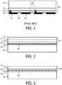
- Fig. 1is a cross-sectional view of a small portion of a prior art device wafer 10, which may include LEDs or any IC devices.
- the device wafer 10may initially include a growth substrate 12, such as a silicon wafer (for an IC wafer) or a sapphire or SiC wafer (for a GaN based LED wafer).
- the device wafer 10is an LED wafer, where only two LED areas of the LED wafer are shown for simplicity. There may be thousands of LED areas on a single LED wafer, where each LED area is on the order of 1 mm 2 .
- the device wafer 10includes an n-type layer 14, an active layer 16 that emits light, and a p-type layer 18.
- a p-metal electrode 20contacts the p-type layer 18, and an n-metal electrode 22 contacts the n-type layer 14.
- a dielectric layer 24insulates the n-metal electrode 22 from the p-type layer 18 and active layer 16.
- a singulation areais shown between dashed lines 26.
- the device wafer 10Since the inventive method is applicable to LED wafers as well as any type of IC wafer, the device wafer 10 has been simplified in the remaining figures to only show certain conductors in the device wafer 10.
- the device wafer 10comprises semiconductor material.
- figures 2 to 12relate to comparative examples useful for understanding the invention, wherein a polymer adhesive 32 is used as a bonding material.
- a metal layeris used to bond the device wafer 10 and the carrier wafer 32.
- Fig. 2illustrates a larger portion of the device wafer 10. Electrodes 28 are shown at the bottom of the device wafer 10. The electrodes 28 may correspond to electrodes 20 and 22 in Fig. 1 . Each device in the device wafer 10 may have any number of electrodes.
- a transparent carrier wafer 30is bonded to the device wafer 10 using a light absorbing polymer adhesive 32. The adhesive 32 may be coated on either the device wafer 10 or the carrier wafer 30, then the two wafers are pressed together while the adhesive 32 is cured. Curing may be by UV, heat, cooling, or other process.
- the carrier wafer 30is selected to be substantially transparent to the laser beam peak wavelength, and the adhesive 32 is selected to absorb a substantial portion of the beam's energy.
- the carrier wafer 30is sapphire or SiC.
- the adhesive 32may be a high temperature (>350°C) polymer such as benzocyclobutene (BCB), polybenzoxazole (PBO), Brewer Science's HT1010TM adhesive (stable up to 240°C), a thermal tape, epoxy, silicone, or a polyimide.
- the carrier wafer 30provides mechanical support for the device wafer 10 during subsequent processing of the device wafer 10.
- all wafers usedare 6 inch wafers, although any size wafers may be used. Standard fabrication tools may be used to handle the carrier wafer 30.
- Fig. 3illustrates device wafer 10 after processing, resulting in the device wafer 10a.
- the growth substrate 12is removed by etching, grinding, or laser lift-off, and the remaining device wafer 10 is thinned to a few tens of microns or less by grinding, polishing, chemical wet etching, or reactive ion etching (RIE).
- the thickness of the device wafer 10amay be in the range of 5-400 microns and preferably 20-200 microns.
- Other processesmay be performed on the device wafer 10a.
- the carrier wafer 30is necessary to provide mechanical support of the thin device wafer 10a so the processes may be performed using standard wafer fabrication tools.
- conductive viasare formed to provide an electrical path through the device wafer 10a.
- the conductive viasmay be used for stacking wafers in a 3-D module, where electrodes on opposing wafer surfaces align and are in electrical contact with each other.
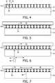
- Fig. 4illustrates via holes 34 etched through the remaining device wafer 10a, such as by masking followed by RIE.
- the via holes 34are then coated with a dielectric, using well-known processes. If the device wafer 10a is silicon, the dielectric is silicon dioxide. Suitable dielectrics and their deposition methods are well known for other device wafer 10a materials.
- the insulated via holes 34then filled with a conductive material 36, such as polysilicon, copper, aluminum, or any other suitable metal or alloy.
- a conductive material 36such as polysilicon, copper, aluminum, or any other suitable metal or alloy.
- the conductive material 36may be deposited by sputtering, plating, or other process.
- a metal electrode layeris then deposited and patterned over the exposed surface to form electrodes 38 contacting the conductive material 36 in filing via holes 34.
- the electrodes 38may comprise gold or other suitable metal, including alloys.
- a conductive pathis formed between opposing surfaces of the device wafer 10a.
- conductive material 36may only fill a portion of via holes 34.
- Fig. 5illustrates a stretchable tacky tape 42 affixed to a surface of the device wafer 10a, which is used to support the dies after singulation, described later.
- Fig. 6illustrates a laser 44 generating a laser beam 46 that is X-Y scanned (or stepped) through the transparent carrier wafer 30 using conventional scanning optics (e.g., lenses, mirrors, prisms, etc.).
- the beam energyis absorbed by the adhesive 32 but not the carrier wafer 30.
- the absorbed energybreaks the chemical bonds between the polymer adhesive 32 and the carrier wafer 30.
- the carrier wafer 30is sapphire, and a 248 nm laser 44 is used. A near-UV or blue laser may also be used.
- a UV laser emitting a peak wavelength of 193nm with an energy intensity of 800 mJ/cm 2is used to de-bond a benzocyclobutene (BCB) polymer adhesive 32 that is stable up to 350°C.
- BCBbenzocyclobutene
- the de-bonding process for a 6-inch diameter waferwill typically take between 5-10 minutes, depending on scan speed, beam energy, beam area, adhesive characteristics, etc. Much shorter de-bonding times are expected with optimized process parameters.
- the inventorshave successfully de-bonded the carrier wafer 30 with adhesives 8-100 microns thick.
- the released carrier wafer 30is then lifted off the device wafer 10a, such as using a mechanical tool or other means.
- gasis released from the adhesive 32 during the absorption of energy and forces the carrier wafer 30 away from the device wafer 10a.
- Fig. 7illustrates the remaining portion of the device wafer 10a after the removal of the de-bonded carrier wafer 30 and the remaining adhesive 32.
- the remaining materialmay be removed by an etchant, plasma, or dissolving solution provided by the manufacturer of the adhesive 32, to expose the electrodes 28.
- An HT1010TM adhesivecan be cleaned easily with a standard HT1010 de-bond remover from Brewer Science.
- an 02/SF6 (for BCB) or 02 (for PBO) plasma etchhas been used with good results.
- the electrodes 28 of the resulting device wafer 10amay then be bonded to aligned electrodes on another wafer 50 or sandwiched between two wafers, where each wafer may provide additional circuitry in a 3-D module.
- the aligned wafer electrodesmay be bonded by ultrasonic bonding under pressure, or by gold balls, or by solder, etc.
- the modulesare then singulated, such as by sawing, laser singulation, water jet cutting, etc., and the tape 42 is then X-Y stretched to separate the modules in preparation for the modules to be packaged or mounted on another wafer or a printed circuit board.
- the dashed line 48illustrates one possible singulation line.
- the device wafer 10a of Fig. 7contains TVS circuitry, such as back-to-back diodes, and/or control circuitry, and the wafer 50 is the LED wafer shown in Fig. 1 , so that each LED is protected by associated TVS circuitry.
- the TVS circuitryprovides a virtual short circuit across the LEDs to protect them when there is a sufficiently high reverse voltage across the LEDs.
- the resulting modules, after singulation,may then be mounted on another wafer containing integrated circuitry or on a submount wafer.
- the submount wafermay be ceramic with electrodes for contacting the electrodes 38 of the device wafer 10a, where the submount electrodes lead to metal pads for bonding to a printed circuit board (PCB).
- PCBprinted circuit board
- the bonded wafer structuremay be mounted on a vacuum chuck, prior to the tape 42 being applied, for cleaning the device wafer 10a after the carrier wafer 30 has been de-bonded. After cleaning, the tape 42 is affixed to the cleaned surface.
- Figs. 8-12illustrate a double bonding method where device wafer 10 is sandwiched between two wafers.
- Fig. 8is similar to Fig. 2 , where a transparent carrier wafer 30 is bonded to the device wafer 10 using a polymer adhesive 32.
- the device wafer 10may be an LED wafer or any IC wafer.
- Fig. 9illustrates the device wafer 10a after removal of its growth substrate 12 ( Fig. 1 ) (if appropriate), and the device wafer 10a being further processed (e.g., thinned).
- a second device wafer 54such as an LED wafer or any IC wafer, having electrodes 56, is bonded to the device wafer 10a by an adhesive 58.
- the adhesive 58is intended to be permanent.
- the adhesive 58is a very high temperature polymer (e.g., >300°C) so as to be unaffected by downstream high temperature processes.
- Fig. 10aillustrates a laser 44 generating a laser beam 46 scanning (or stepping) through the transparent carrier wafer 30.
- the beam energyis absorbed by the adhesive 32 but not the carrier wafer 30.
- the absorbed energybreaks the chemical bonds between the polymer adhesive 32 and the carrier wafer 30.
- the released carrier wafer 30is then lifted off the device wafer 10a.
- Fig. 11illustrates the de-bonded carrier wafer 30 removed from the device wafer 10a and the remaining adhesive 32 removed to expose the electrodes 28.
- Fig. 12illustrates via holes 62 etched through the remaining device wafer 10a and the adhesive 58 using RIE or other means.
- the via holes 62are then coated with a dielectric 63 (if the device wafer 10a body is not an insulating material) using well-known processes, and the via holes 62 are then filled with a conductive material 64.
- a metal electrode layeris then deposited and patterned over the exposed surface to form electrodes 66 contacting the conductive material 64 and/or the electrodes 28.
- the electrodes 66may comprise gold or any suitable alloy.
- a conductive pathis formed between the electrodes 56 of the second device wafer 54 and the "bottom" electrodes 28 of the device wafer 10a.
- the second device wafer 54contains active control circuitry 67 for controlling LEDs
- the device wafer 10acontains TVS circuitry 68 (only one TVS circuit 68 is shown connected to the electrodes 66 for simplicity)
- the LED wafer electrodes 20 and 22 (for each LED) of Fig. 1are bonded to the electrodes 28 of the device wafer 10a.
- the control circuitry 67 and TVS circuitry 68may be otherwise conventional.
- the second device wafer 54may itself have through-hole vias terminating in pads for bonding to a PCB. Alternatively, after singulation, the electrodes 66 are bonded to pads of a PCB, and the device wafer 10a acts as an interface between the PCB pads and the second device wafer 54.
- control circuitryis provided as a separate chip on a PCB electrically connected to the LEDs by traces on the PCB.
- the 3-D module combining the LEDs and control circuitry on a single dieallows for extremely compact applications, such as the use of the module as a flash in a smart phone camera.
- the LED wafer of Fig. 1is the second device wafer 54
- the device wafer 10acontains TVS circuitry and/or control circuitry for the LEDs
- the electrodes 66are bonded to pads of a PCB for providing power and control signals for the LEDs.
- the device wafers 10a and 54may include active circuitry (transistors, diodes, etc.), passive circuitry (conductors, resistors, capacitors, etc.), or any other circuitry.
- the resulting 3-D wafermay be singulated along line 72 to form 3-D module dies for packaging.
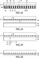
- Figs. 13-15illustrate the use of a metal-metal bond between the device wafer and the carrier wafer, according to the invention.
- Fig. 13illustrates a first metal layer 80 (such as a eutectic alloy) deposited on the device wafer 10a by, for example, sputtering.
- the metal layer 80may be gold or a suitable eutectic alloy. The bond need not be strong.
- a second metal layer 82(such as a eutectic alloy) is deposited on the transparent carrier wafer 30 by, for example, sputtering.
- the metal layers 80 and 82may have the same composition. The metal bonds to the wafers need not be strong.
- Suitable metals and alloysinclude combinations of Au, Cu, Ag, Al, Sn, SiGe, and Si.
- the metal layers 80 and 82are then bonded together using heat and pressure, such as by ultrasonic welding or externally applied heat.
- the metal-metal bondcan withstand higher temperatures than available polymer adhesives, so the process of Figs. 13-15 is particularly suitable when very high temperature processes (>400°C) need to be performed on the device wafer 10a.
- Fig. 14illustrates a laser beam 46 scanning through the carrier wafer 30 to break the bonds between the deposited metal layer 82 and the carrier wafer 30. The bonds between metal and a sapphire carrier wafer 30 are easily broken.
- Fig. 15illustrates the device wafer 10a after the carrier wafer 30 has been removed.
- the remaining metal layers 80 and 82are then etched from the device wafer 10a or removed by other means.
- the metal layers 80 and 82are retained as electrodes or a reflector layer.
- the device wafer 10ais then singulated, as previously described.
- the de-bonding techniquemay also be applied to other types of bonding techniques/materials, such as anodic bonding, fusion bonding, frit glass bonding, etc.
Landscapes
- Engineering & Computer Science (AREA)
- Microelectronics & Electronic Packaging (AREA)
- Computer Hardware Design (AREA)
- Power Engineering (AREA)
- Physics & Mathematics (AREA)
- Condensed Matter Physics & Semiconductors (AREA)
- Manufacturing & Machinery (AREA)
- General Physics & Mathematics (AREA)
- Optics & Photonics (AREA)
- Led Devices (AREA)
- Laser Beam Processing (AREA)
- Dicing (AREA)
- Drying Of Semiconductors (AREA)
- Mechanical Treatment Of Semiconductor (AREA)
Description
- This invention relates to semiconductor wafer fabrication and, in particular, to a process for de-bonding a carrier wafer from a device wafer containing electrical components, where the carrier wafer provides temporary mechanical support for the device wafer during processing of the device wafer.
- Although the invention applies to the fabrication of virtually any type of semiconductor device wafer, an example of fabricating a light emitting diode (LED) wafer is presented.
- Gallium nitride based LEDs, such as for generating blue light, are manufactured by epitaxially growing semiconductor layers over a growth substrate (a wafer), such as sapphire. An active layer between p-type and n-type layers emits light having a peak wavelength, and the peak wavelength is determined by the material composition of the active layer. Such semiconductor layers may be on the order of a few tens of microns thick and very brittle. Metallization and other well-known processes are then performed on the LED wafer to, for example, remove the growth substrate, thin the LED layers, and form electrodes. The LED wafer is subsequently diced to form LED chips for packaging.
- In cases where the growth substrate is to be removed from the LED wafer, such as to perform processes on the LED layers facing the growth substrate, or in cases where the growth substrate is to be thinned, such as for scribe and break singulation, a carrier wafer must be first bonded to the opposite surface of the LED wafer to provide mechanical support of the thin LED layers during removal or thinning of the growth substrate. After the carrier wafer is bonded to the LED wafer and the growth substrate is removed or thinned, any exposed LED layers may be further processed, such as thinning the LED layers and depositing thin films over the exposed LED layers. The carrier wafer may be connected temporarily or permanently. If the carrier wafer is temporary, methods have to be performed to de-bond the carrier wafer from the LED wafer. Silicon carrier wafers are commonly used due to their low cost and well-known characteristics. A silicon carrier wafer absorbs light from the LED and should be ultimately removed from the LED layers.
- Using a carrier wafer (typically silicon) for mechanical support is commonly used in integrated circuit processes, especially where IC wafers are stacked to form three-dimensional (3-D) modules and conductive vias extend vertically though the IC wafers. Typically, the carrier wafer is bonded to the IC wafer using an intermediate-temperature (e.g., up to 250°C) polymer adhesive so that the adhesive does not release at the expected IC wafer process temperatures. After the IC wafer processing is completed, de-bonding of the carrier wafer is performed at a high heat and with special tools and techniques (e.g., using Brewer Science's HT1010™ thermal-sliding de-bond process).
- It is also known to apply a special light-to-heat conversion (LTHC) layer over a carrier wafer, then bond the carrier wafer to the device wafer using a special adhesive that melts at a relatively low temperature. A laser beam is then used to heat up the LTHC layer, which, in turn, melts the adhesive for de-bonding the carrier wafer. The LTHC material, special adhesive materials (e.g., 3M's LC3200 and LC5200), and special tools are available from 3M Company. The process is relatively expensive and time-consuming. Since the adhesive needs to melt at a relatively low temperature (the 3M adhesive is rated only up to 180°C), the de-bonding process is not suitable when quality thin films need to be deposited, since such thin films typically need to be deposited at over 250°C.
US2011/101413 A1 describes a method of manufacturing a semiconductor device. In the method, a growth substrate provided with a single crystal semiconductor thin layer, a support substrate, and a temporary substrate are prepared, the growth substrate, the support substrate, and the temporary substrate are bonded to one another with the support substrate therebetween through functional wafer coupling layers, the growth substrate is lifted off from the single crystal semiconductor thin layer, and the temporary substrate is lifted off from the support substrate.EP2262012A2 describes a light emitting device including a support substrate; a reflective layer over the support substrate; an ohmic contact layer over the reflective layer; a light emitting semiconductor layer including a second conductive semiconductor layer, an active layer and a first conductive semiconductor layer over the ohmic contact layer; a first passivation layer surrounding a lateral side of the light emitting semiconductor layer; and a second passivation layer surrounding lateral sides of the first passivation layer and the reflective layer.- In some processes for forming high quality thin films, such as a PECVD process, the process temperature is substantially greater than 250°C. The polymers used for temporarily bonding the carrier wafer to the IC or LED wafer must therefore be very high temperature polymers (e.g., > 350°C), requiring more complex and higher temperature de-bonding processes and tools.
- What is needed is an improved technique for de-bonding a carrier wafer from a device wafer that is simpler than the prior art processes, and that works with metal (e.g., eutectic alloy) bonding materials.
- Instead of a light absorbing carrier wafer, such as silicon, a transparent carrier wafer is used, such as a sapphire or SiC wafer. In the example of an LED wafer process, the carrier wafer is bonded to the LED wafer opposite the side that is supported by the growth substrate. The bonding material is, in comparative examples not forming part of the invention, a conventional polymer adhesive, such as a polymer that is stable up to 350°C. In embodiments of the invention, the bonding material comprises a first metal layer and the second metal layer, see below.
- The growth substrate is then removed from the LED wafer, and the exposed LED layers are further processed. Such further processing may include thinning, depositing thin films, forming vias, etc. The growth substrate may be thinned instead of removed. The device wafer may be any wafer containing circuitry.
- For de-bonding the carrier wafer from the LED wafer, a laser beam is scanned over the carrier wafer, where the carrier wafer is substantially transparent to the wavelength of light from the laser beam. The polymer adhesive, used in as comparative example, directly absorbs the laser beam energy, and the energy breaks the polymer-carrier chemical bonds, rather than simply melting the polymer through heat. There is no light-to-heat conversion (LTHC) layer used, so special materials are not needed. The laser is not strong enough to damage any structures within the LED wafer. In one embodiment, a 248 nm laser is used. A near-UV or blue laser may also be used.
- Further, in comparative examples , a UV laser emitting a peak wavelength of 193nm with an energy intensity of 800 mJ/cm2 (40W/cm2) is used to de-bond a benzocyclobutene (BCB) polymer adhesive that is stable up to 350°C.
- Accordingly, the adhesive does not require heat to be released so can be an adhesive that is stable at sufficiently high temperatures for thin film processing.
- After the removal of the carrier wafer, the de-bonded surface of the LED wafer is then cleaned of the residual adhesive.
- Hence, in an aspect, the invention provides a method for forming an electrical structure comprising: providing a semiconductor first device wafer containing first electrical components, the first device wafer having first electrodes on a first side of the first device wafer; depositing a first metal layer on the first side of the first device wafer and on the first electrodes, thereby providing metal bonds between the first metal layer and the first device wafer (1); depositing a second metal layer on a carrier wafer, thereby providing metal bonds between the second metal layer and the carrier wafer; and bonding the first metal layer to the second metal layer using heat and pressure, thereby bonding the carrier wafer to the first side of the first device wafer using a first bonding material, wherein the first bonding material comprises the first metal layer and the second metal layer bonded together, wherein a metal-metal bond is formed between the first metal layer and the second metal layer; processing a second side of the first device wafer while the carrier wafer is bonded to the first device wafer; passing light from a laser through the carrier wafer to impinge on the first bonding material, wherein a laser beam is scanned over the carrier wafer, the first bonding material absorbing energy from the laser beam, the carrier wafer being substantially transparent to the light from the laser, wherein the first bonding material substantially releases the carrier wafer from the first device wafer due to energy in the light from the laser breaking the bonds between the second metal layer and the carrier wafer; removing the carrier wafer from the first device wafer; and removing any residual first bonding material from the first device wafer.
- In embodiments of the invention, a metal layer, such as a suitable eutectic metal alloy layer, is deposited on both the device wafer and the transparent carrier wafer (e.g., sapphire). The wafers are then bonded together under heat and pressure without any additional adhesive. A laser beam is then scanned through the carrier wafer, where the laser energy breaks the chemical bonds between the metal layer and the transparent carrier wafer, which de-bonds the carrier wafer from the metal layer. The metal layers remaining on the device wafer are then be etched/cleaned before singulation. In comparative examples not forming part of the invention, the metal layers may be used as a reflector and/or an electrode for the device wafer and do not need to be removed before singulation.
- In comparative examples not forming part of the invention, the de-bonding technique may also be applied to other types of bonding techniques/materials, such as anodic bonding, fusion bonding, frit glass bonding, etc.
- The de-bonding process may be used for any type of IC wafer and is not limited to LED applications. All such wafers are referred to herein as device wafers.
- Various other examples of processes are also described, such as a process for forming conductive vias through wafers for three-dimensional modules.
Fig. 1 is a cross-sectional view of a small portion of a prior art LED wafer, including a growth substrate, showing two LED areas for simplicity. The LED wafer is hereinafter referred to as a device wafer, since the de-bonding process may be performed with any type of wafer.Fig. 2 illustrates a larger portion of the device wafer ofFig. 1 and eliminates detail of the LEDs for simplicity. A transparent carrier wafer is bonded to the device wafer using a polymer adhesive that absorbs UV or blue laser light.Fig. 3 illustrates the structure ofFig. 2 after the growth substrate is removed (if appropriate for the device wafer) and after the exposed device wafer is thinned or otherwise further processed.Fig. 4 illustrates via holes etched through the remaining device wafer, where the via holes are then coated with a dielectric and filled with a conductive material. A patterned electrode layer is then formed for terminating the conductive vias. The vias create conductive paths between opposing surfaces of the device wafer.Fig. 5 illustrates a stretchable tacky tape affixed to a surface of the device wafer.Fig. 6 illustrates a laser beam scanning through the transparent carrier wafer and its energy being absorbed by the polymer adhesive to break the chemical bonds between the polymer and the carrier wafer.Fig. 7 illustrates the de-bonded carrier wafer removed and the remaining polymer adhesive removed. The remaining portion of the device wafer with the through-hole vias may then be bonded to another wafer or sandwiched between two wafers for providing additional circuitry in a 3-D module. The modules are then singulated, such as by sawing, and the tape is then stretched to separate the modules in preparation for the modules to be packaged.Figs. 8-12 illustrate a double bonding method where the device wafer is sandwiched between two wafers.Fig. 8 is similar toFig. 2 , where a transparent carrier wafer is bonded to the device wafer. The device wafer may be an LED wafer or any IC wafer.Fig. 9 illustrates the device wafer having its growth substrate removed (if appropriate), followed by the device wafer being further processed (e.g., thinned), followed by another wafer being bonded to the exposed surface by a polymer adhesive.Fig. 10 illustrates a laser beam scanning through the transparent carrier wafer and its energy being absorbed by the polymer adhesive to break the chemical bonds between the polymer and the carrier wafer.Fig. 11 illustrates the de-bonded carrier wafer removed and the remaining polymer adhesive removed.Fig. 12 illustrates via holes etched through the remaining device wafer, where the via holes are then coated with a dielectric and filled with a conductive material. A patterned electrode layer is then formed for terminating the conductive vias. The vias create conductive paths between opposing surfaces of the device wafer. The upper wafer bonded to the device wafer may contain transient voltage suppression (TVS) circuitry (e.g., ESD protection circuitry) or control circuitry for the devices on the device wafer. The resulting 3-D module is then singulated, as previously described with respect toFig. 7 .Figs. 13-15 illustrate the use of a metal-metal bond between the device wafer and the carrier wafer, according to an embodiment of the invention.Fig. 13 illustrates metal (including alloys) layers deposited on the device wafer and the transparent carrier wafer and the metal layers being bonded together using heat and pressure.Fig. 14 illustrates a laser beam scanning through the carrier wafer to break the bonds between the deposited metal layer and the carrier wafer.Fig. 15 illustrates the device wafer after the carrier wafer has been removed.- Elements that are the same or equivalent are labeled with the same numeral.
Fig. 1 is a cross-sectional view of a small portion of a priorart device wafer 10, which may include LEDs or any IC devices. Thedevice wafer 10 may initially include agrowth substrate 12, such as a silicon wafer (for an IC wafer) or a sapphire or SiC wafer (for a GaN based LED wafer). In the example ofFig. 1 , thedevice wafer 10 is an LED wafer, where only two LED areas of the LED wafer are shown for simplicity. There may be thousands of LED areas on a single LED wafer, where each LED area is on the order of 1 mm2.- The
device wafer 10 includes an n-type layer 14, anactive layer 16 that emits light, and a p-type layer 18. A p-metal electrode 20 contacts the p-type layer 18, and an n-metal electrode 22 contacts the n-type layer 14. Adielectric layer 24 insulates the n-metal electrode 22 from the p-type layer 18 andactive layer 16. A singulation area is shown between dashedlines 26. - Since the inventive method is applicable to LED wafers as well as any type of IC wafer, the
device wafer 10 has been simplified in the remaining figures to only show certain conductors in thedevice wafer 10. Thedevice wafer 10 comprises semiconductor material. - The following description of
figures 2 to 12 relates to comparative examples useful for understanding the invention, wherein apolymer adhesive 32 is used as a bonding material. In embodiments of the invention a metal layer is used to bond thedevice wafer 10 and thecarrier wafer 32. Fig. 2 illustrates a larger portion of thedevice wafer 10.Electrodes 28 are shown at the bottom of thedevice wafer 10. Theelectrodes 28 may correspond toelectrodes Fig. 1 . Each device in thedevice wafer 10 may have any number of electrodes. Atransparent carrier wafer 30 is bonded to thedevice wafer 10 using a light absorbingpolymer adhesive 32. The adhesive 32 may be coated on either thedevice wafer 10 or thecarrier wafer 30, then the two wafers are pressed together while the adhesive 32 is cured. Curing may be by UV, heat, cooling, or other process. Since a laser beam will eventually be used to break the chemical bonds between the adhesive 32 and thecarrier wafer 30, thecarrier wafer 30 is selected to be substantially transparent to the laser beam peak wavelength, and the adhesive 32 is selected to absorb a substantial portion of the beam's energy. In one embodiment, thecarrier wafer 30 is sapphire or SiC. The adhesive 32 may be a high temperature (>350°C) polymer such as benzocyclobutene (BCB), polybenzoxazole (PBO), Brewer Science's HT1010™ adhesive (stable up to 240°C), a thermal tape, epoxy, silicone, or a polyimide.- The
carrier wafer 30 provides mechanical support for thedevice wafer 10 during subsequent processing of thedevice wafer 10. In one embodiment, all wafers used are 6 inch wafers, although any size wafers may be used. Standard fabrication tools may be used to handle thecarrier wafer 30. Fig. 3 illustratesdevice wafer 10 after processing, resulting in thedevice wafer 10a. In the example, thegrowth substrate 12 is removed by etching, grinding, or laser lift-off, and the remainingdevice wafer 10 is thinned to a few tens of microns or less by grinding, polishing, chemical wet etching, or reactive ion etching (RIE). The thickness of thedevice wafer 10a may be in the range of 5-400 microns and preferably 20-200 microns. Other processes may be performed on thedevice wafer 10a. Thecarrier wafer 30 is necessary to provide mechanical support of thethin device wafer 10a so the processes may be performed using standard wafer fabrication tools.- In one example, conductive vias are formed to provide an electrical path through the
device wafer 10a. The conductive vias may be used for stacking wafers in a 3-D module, where electrodes on opposing wafer surfaces align and are in electrical contact with each other. Fig. 4 illustrates viaholes 34 etched through the remainingdevice wafer 10a, such as by masking followed by RIE. The via holes 34 are then coated with a dielectric, using well-known processes. If thedevice wafer 10a is silicon, the dielectric is silicon dioxide. Suitable dielectrics and their deposition methods are well known forother device wafer 10a materials.- The insulated via
holes 34 then filled with aconductive material 36, such as polysilicon, copper, aluminum, or any other suitable metal or alloy. Theconductive material 36 may be deposited by sputtering, plating, or other process. - A metal electrode layer is then deposited and patterned over the exposed surface to form
electrodes 38 contacting theconductive material 36 in filing via holes 34. Theelectrodes 38 may comprise gold or other suitable metal, including alloys. Thus, a conductive path is formed between opposing surfaces of thedevice wafer 10a. In the alternativeconductive material 36 may only fill a portion of via holes 34. Fig. 5 illustrates a stretchabletacky tape 42 affixed to a surface of thedevice wafer 10a, which is used to support the dies after singulation, described later.Fig. 6 illustrates alaser 44 generating alaser beam 46 that is X-Y scanned (or stepped) through thetransparent carrier wafer 30 using conventional scanning optics (e.g., lenses, mirrors, prisms, etc.). In the examples comprising the adhesive 32 for bonding thedevice wafer 10 and thecarrier wafer 32, the beam energy is absorbed by the adhesive 32 but not thecarrier wafer 30. The absorbed energy breaks the chemical bonds between thepolymer adhesive 32 and thecarrier wafer 30. In one embodiment, thecarrier wafer 30 is sapphire, and a 248nm laser 44 is used. A near-UV or blue laser may also be used. In another embodiment, a UV laser emitting a peak wavelength of 193nm with an energy intensity of 800 mJ/cm2 (40W/cm2) is used to de-bond a benzocyclobutene (BCB)polymer adhesive 32 that is stable up to 350°C. The de-bonding process for a 6-inch diameter wafer will typically take between 5-10 minutes, depending on scan speed, beam energy, beam area, adhesive characteristics, etc. Much shorter de-bonding times are expected with optimized process parameters. The inventors have successfully de-bonded thecarrier wafer 30 with adhesives 8-100 microns thick.- The released
carrier wafer 30 is then lifted off thedevice wafer 10a, such as using a mechanical tool or other means. In one embodiment, gas is released from the adhesive 32 during the absorption of energy and forces thecarrier wafer 30 away from thedevice wafer 10a. Fig. 7 illustrates the remaining portion of thedevice wafer 10a after the removal of thede-bonded carrier wafer 30 and the remainingadhesive 32. The remaining material may be removed by an etchant, plasma, or dissolving solution provided by the manufacturer of the adhesive 32, to expose theelectrodes 28. An HT1010™ adhesive can be cleaned easily with a standard HT1010 de-bond remover from Brewer Science. For higher temperature adhesives, such as BCB or PBO, an 02/SF6 (for BCB) or 02 (for PBO) plasma etch has been used with good results.- The
electrodes 28 of the resultingdevice wafer 10a may then be bonded to aligned electrodes on anotherwafer 50 or sandwiched between two wafers, where each wafer may provide additional circuitry in a 3-D module. The aligned wafer electrodes may be bonded by ultrasonic bonding under pressure, or by gold balls, or by solder, etc. The modules are then singulated, such as by sawing, laser singulation, water jet cutting, etc., and thetape 42 is then X-Y stretched to separate the modules in preparation for the modules to be packaged or mounted on another wafer or a printed circuit board. The dashedline 48 illustrates one possible singulation line. - In one embodiment, the
device wafer 10a ofFig. 7 contains TVS circuitry, such as back-to-back diodes, and/or control circuitry, and thewafer 50 is the LED wafer shown inFig. 1 , so that each LED is protected by associated TVS circuitry. The TVS circuitry provides a virtual short circuit across the LEDs to protect them when there is a sufficiently high reverse voltage across the LEDs. The resulting modules, after singulation, may then be mounted on another wafer containing integrated circuitry or on a submount wafer. The submount wafer may be ceramic with electrodes for contacting theelectrodes 38 of thedevice wafer 10a, where the submount electrodes lead to metal pads for bonding to a printed circuit board (PCB). - Alternatively, the bonded wafer structure may be mounted on a vacuum chuck, prior to the
tape 42 being applied, for cleaning thedevice wafer 10a after thecarrier wafer 30 has been de-bonded. After cleaning, thetape 42 is affixed to the cleaned surface. Figs. 8-12 illustrate a double bonding method wheredevice wafer 10 is sandwiched between two wafers.Fig. 8 is similar toFig. 2 , where atransparent carrier wafer 30 is bonded to thedevice wafer 10 using apolymer adhesive 32. Thedevice wafer 10 may be an LED wafer or any IC wafer.Fig. 9 illustrates thedevice wafer 10a after removal of its growth substrate 12 (Fig. 1 ) (if appropriate), and thedevice wafer 10a being further processed (e.g., thinned). Asecond device wafer 54, such as an LED wafer or any IC wafer, havingelectrodes 56, is bonded to thedevice wafer 10a by an adhesive 58. Unlike the adhesive 32, which absorbs the laser beam energy for de-bonding, the adhesive 58 is intended to be permanent. In one embodiment, the adhesive 58 is a very high temperature polymer (e.g., >300°C) so as to be unaffected by downstream high temperature processes.Fig. 10a , as inFig. 6 , illustrates alaser 44 generating alaser beam 46 scanning (or stepping) through thetransparent carrier wafer 30. As described with respect toFig. 6 , the beam energy is absorbed by the adhesive 32 but not thecarrier wafer 30. The absorbed energy breaks the chemical bonds between thepolymer adhesive 32 and thecarrier wafer 30. The releasedcarrier wafer 30 is then lifted off thedevice wafer 10a.Fig. 11 illustrates thede-bonded carrier wafer 30 removed from thedevice wafer 10a and the remainingadhesive 32 removed to expose theelectrodes 28.Fig. 12 , as inFig. 4 , illustrates viaholes 62 etched through the remainingdevice wafer 10a and the adhesive 58 using RIE or other means. The via holes 62 are then coated with a dielectric 63 (if thedevice wafer 10a body is not an insulating material) using well-known processes, and the via holes 62 are then filled with aconductive material 64. A metal electrode layer is then deposited and patterned over the exposed surface to formelectrodes 66 contacting theconductive material 64 and/or theelectrodes 28. Theelectrodes 66 may comprise gold or any suitable alloy. Thus, a conductive path is formed between theelectrodes 56 of thesecond device wafer 54 and the "bottom"electrodes 28 of thedevice wafer 10a.- In one example, the
second device wafer 54 containsactive control circuitry 67 for controlling LEDs, thedevice wafer 10a contains TVS circuitry 68 (only oneTVS circuit 68 is shown connected to theelectrodes 66 for simplicity), and theLED wafer electrodes 20 and 22 (for each LED) ofFig. 1 are bonded to theelectrodes 28 of thedevice wafer 10a. Thecontrol circuitry 67 andTVS circuitry 68 may be otherwise conventional. Thesecond device wafer 54 may itself have through-hole vias terminating in pads for bonding to a PCB. Alternatively, after singulation, theelectrodes 66 are bonded to pads of a PCB, and thedevice wafer 10a acts as an interface between the PCB pads and thesecond device wafer 54. In conventional LED systems, the control circuitry is provided as a separate chip on a PCB electrically connected to the LEDs by traces on the PCB. The 3-D module combining the LEDs and control circuitry on a single die allows for extremely compact applications, such as the use of the module as a flash in a smart phone camera. - In another example, embodiment, the LED wafer of
Fig. 1 is thesecond device wafer 54, thedevice wafer 10a contains TVS circuitry and/or control circuitry for the LEDs, and theelectrodes 66 are bonded to pads of a PCB for providing power and control signals for the LEDs. Many other variations of circuitry are envisioned. Thedevice wafers - The resulting 3-D wafer may be singulated along line 72 to form 3-D module dies for packaging.
Figs. 13-15 illustrate the use of a metal-metal bond between the device wafer and the carrier wafer, according to the invention.Fig. 13 illustrates a first metal layer 80 (such as a eutectic alloy) deposited on thedevice wafer 10a by, for example, sputtering. Themetal layer 80 may be gold or a suitable eutectic alloy. The bond need not be strong.- A second metal layer 82 (such as a eutectic alloy) is deposited on the
transparent carrier wafer 30 by, for example, sputtering. The metal layers 80 and 82 may have the same composition. The metal bonds to the wafers need not be strong. - Suitable metals and alloys include combinations of Au, Cu, Ag, Al, Sn, SiGe, and Si.
- The metal layers 80 and 82 are then bonded together using heat and pressure, such as by ultrasonic welding or externally applied heat. The metal-metal bond can withstand higher temperatures than available polymer adhesives, so the process of
Figs. 13-15 is particularly suitable when very high temperature processes (>400°C) need to be performed on thedevice wafer 10a. Fig. 14 illustrates alaser beam 46 scanning through thecarrier wafer 30 to break the bonds between the depositedmetal layer 82 and thecarrier wafer 30. The bonds between metal and asapphire carrier wafer 30 are easily broken.Fig. 15 illustrates thedevice wafer 10a after thecarrier wafer 30 has been removed. The remainingmetal layers device wafer 10a or removed by other means. In some comparative examples not forming part of the invention, the metal layers 80 and 82 are retained as electrodes or a reflector layer.- The
device wafer 10a is then singulated, as previously described. - In comparative examples not forming part of the invention, the de-bonding technique may also be applied to other types of bonding techniques/materials, such as anodic bonding, fusion bonding, frit glass bonding, etc.
- While particular embodiments and elements of the present invention have been shown and described, it will be obvious to those skilled in the art that changes and modifications may be made without departing from the scope of the appended claims. The appended claims are to encompass within their scope all such changes and modifications.
Claims (13)
- A method for forming an electrical structure comprising:providing a semiconductor first device wafer (10) containing first electrical components, the first device wafer (10) having first electrodes (28) on a first side of the first device wafer (10);depositing a first metal layer (80) on the first side of the first device wafer (10) and on the first electrodes (28), thereby providing metal bonds between the first metal layer (80) and the first device wafer (1);depositing a second metal layer (82) on a carrier wafer (30), thereby providing metal bonds between the second metal layer (82) and the carrier wafer (30); andbonding the first metal layer (80) to the second metal layer (82) using heat and pressure, thereby bonding the carrier wafer (30) to the first side of the first device wafer (10) using a first bonding material, wherein the first bonding material comprises the first metal layer (80) and the second metal layer (82) bonded together, wherein a metal-metal bond is formed between the first metal layer (80) and the second metal layer (82);processing a second side of the first device wafer (10) while the carrier wafer (30) is bonded to the first device wafer (10);passing light from a laser (44) through the carrier wafer (30) to impinge on the first bonding material, wherein a laser beam (46) is scanned over the carrier wafer, the first bonding material absorbing energy from the laser beam (46), the carrier wafer (30) being transparent to the light from the laser (44), wherein the first bonding material releases the carrier wafer (30) from the first device wafer (10) due to energy in the light from the laser (44) breaking the metal bonds between the second metal layer (82) and the carrier wafer (30);removing the carrier wafer (30) from the first device wafer (10); andremoving any residual first bonding material from the first device wafer (10).
- The method of Claim 1 wherein the device wafer (10) includes an n-type layer (14), a p-type layer (18), and an active layer (16) between the n-type layer (14) and the p-type layer(18) and configured for emitting light, wherein a p-metal electrode (20) contacts the p-type layer (18), and an n-metal electrode (22) contacts the n-type layer (14), wherein a dielectric layer (24) insulates the n-metal electrode (22) from the p-type layer (18) and from the active layer (16), and wherein first electrodes comprise the p-metal electrode (20) and the n-metal electrode (22).
- The method of any one of claims 1-2 wherein the first bonding material comprises a metal alloy layer.
- The method of any one of claims 1-2 wherein the wavelength of the light from the laser (44) ranges between UV and blue.
- The method of claim 4, wherein the wavelength of the light from the laser (44) is in the UV range.
- The method of any one of claims 1-2 wherein the carrier wafer (30) comprises sapphire.
- The method of any one of claims 1-2, wherein the carrier wafer (30) comprises SiC.
- The method of any one of claims 1-2, wherein the step of processing the second side of the first device wafer (10) comprises forming conductive vias through the first device wafer (10).
- The method of Claim 8 further comprising bonding a second device wafer (54) to the first device wafer (10) such that the conductive vias contact electrodes on the second device wafer (54) for forming a three-dimensional module after the first device wafer (10) and the second device wafer (54) are singulated.
- The method of Claim 9 wherein the second device wafer (54) contains light emitting diodes (LEDs).
- The method of Claim 10 wherein the first device wafer (10) contains transient voltage suppression (TVS) circuitry for the LEDs.
- The method of any one of claims 1-2 wherein the first device wafer (10) contains light emitting diodes (LEDs).
- The method according to any one of the preceding claims, wherein the first metal layer (80) includes a combination of Au, Cu, Ag, Al, Sn, SiGe, and Si; and/or wherein the second metal layer (82) includes a combination of Au, Cu, Ag, Al, Sn, SiGe, and Si.
Applications Claiming Priority (2)
| Application Number | Priority Date | Filing Date | Title |
|---|---|---|---|
| US201261696943P | 2012-09-05 | 2012-09-05 | |
| PCT/IB2013/056588WO2014037829A1 (en) | 2012-09-05 | 2013-08-12 | Laser de-bond of carrier wafer from device wafer |
Publications (2)
| Publication Number | Publication Date |
|---|---|
| EP2893565A1 EP2893565A1 (en) | 2015-07-15 |
| EP2893565B1true EP2893565B1 (en) | 2021-04-28 |
Family
ID=49385305
Family Applications (1)
| Application Number | Title | Priority Date | Filing Date |
|---|---|---|---|
| EP13779363.4AActiveEP2893565B1 (en) | 2012-09-05 | 2013-08-12 | Laser de-bond of carrier wafer from device wafer |
Country Status (5)
| Country | Link |
|---|---|
| US (1) | US10741718B2 (en) |
| EP (1) | EP2893565B1 (en) |
| JP (1) | JP6478913B2 (en) |
| CN (1) | CN104584214B (en) |
| WO (1) | WO2014037829A1 (en) |
Families Citing this family (18)
| Publication number | Priority date | Publication date | Assignee | Title |
|---|---|---|---|---|
| US9355881B2 (en)* | 2014-02-18 | 2016-05-31 | Infineon Technologies Ag | Semiconductor device including a dielectric material |
| US20160133486A1 (en) | 2014-11-07 | 2016-05-12 | International Business Machines Corporation | Double Layer Release Temporary Bond and Debond Processes and Systems |
| JP6405465B2 (en)* | 2015-04-01 | 2018-10-17 | ゴルテック.インク | MEMS transport method, manufacturing method, device and equipment |
| EP3218939B1 (en) | 2015-08-18 | 2019-05-22 | Goertek. Inc | Pre-screening method of micro-led |
| TW202524641A (en)* | 2016-01-15 | 2025-06-16 | 荷蘭商庫力克及索發荷蘭公司 | Placing ultra-small or ultra-thin discrete components |
| JP6649111B2 (en)* | 2016-02-16 | 2020-02-19 | 東京応化工業株式会社 | Laminate, method for producing laminate, and method for treating substrate |
| JP6704047B2 (en) | 2016-06-02 | 2020-06-03 | 富士フイルム株式会社 | Pattern manufacturing method, semiconductor device manufacturing method, and laminated body |
| TWI723206B (en) | 2016-08-18 | 2021-04-01 | 日商富士軟片股份有限公司 | Wafer manufacturing method |
| CN106783726A (en)* | 2016-12-30 | 2017-05-31 | 苏州爱彼光电材料有限公司 | Compound substrate and preparation method thereof, semiconductor devices |
| US10269589B2 (en)* | 2017-06-30 | 2019-04-23 | Taiwan Semiconductor Manufacturing Company, Ltd. | Method of manufacturing a release film as isolation film in package |
| US10403598B2 (en) | 2017-08-11 | 2019-09-03 | Micron Technology, Inc. | Methods and system for processing semiconductor device structures |
| DE102018126936A1 (en) | 2018-10-29 | 2020-04-30 | Osram Opto Semiconductors Gmbh | Process for the production of optoelectronic semiconductor components |
| US11195740B2 (en) | 2019-04-17 | 2021-12-07 | Micron Technology, Inc. | Methods and apparatus for wafer handling and processing |
| US20210183803A1 (en)* | 2019-12-17 | 2021-06-17 | Micron Technology, Inc. | Reconstructed wafer to wafer bonding using a permanent bond with laser release |
| EP4158683B1 (en)* | 2020-05-29 | 2024-04-10 | Erich Thallner | Method for bonding and debonding two substrates |
| CN113690183B (en)* | 2021-07-06 | 2024-06-25 | 华为数字能源技术有限公司 | Wafer thinning method |
| JP7708514B2 (en)* | 2021-09-02 | 2025-07-15 | 東京エレクトロン株式会社 | LAMINATED SUBSTRATE FOR LASER LIFT-OFF, SUBSTRATE PROCESSING METHOD, AND SUBSTRATE PROCESSING APPARATUS |
| TW202315155A (en)* | 2021-09-29 | 2023-04-01 | 日商信越半導體股份有限公司 | Method for separating bonded wafer |
Citations (1)
| Publication number | Priority date | Publication date | Assignee | Title |
|---|---|---|---|---|
| US20110101413A1 (en)* | 2008-03-19 | 2011-05-05 | Lg Innotek Co., Ltd. | Semiconductor device and method of manufacturing the same |
Family Cites Families (20)
| Publication number | Priority date | Publication date | Assignee | Title |
|---|---|---|---|---|
| EP0721662A1 (en)* | 1993-09-30 | 1996-07-17 | Kopin Corporation | Three-dimensional processor using transferred thin film circuits |
| JP4619462B2 (en)* | 1996-08-27 | 2011-01-26 | セイコーエプソン株式会社 | Thin film element transfer method |
| USRE38466E1 (en)* | 1996-11-12 | 2004-03-16 | Seiko Epson Corporation | Manufacturing method of active matrix substrate, active matrix substrate and liquid crystal display device |
| JPH1126733A (en)* | 1997-07-03 | 1999-01-29 | Seiko Epson Corp | Transfer method of thin film device, thin film device, thin film integrated circuit device, active matrix substrate, liquid crystal display device, and electronic equipment |
| JP4461616B2 (en)* | 2000-12-14 | 2010-05-12 | ソニー株式会社 | Element transfer method, element holding substrate forming method, and element holding substrate |
| JP4082242B2 (en) | 2003-03-06 | 2008-04-30 | ソニー株式会社 | Element transfer method |
| US7462552B2 (en)* | 2005-05-23 | 2008-12-09 | Ziptronix, Inc. | Method of detachable direct bonding at low temperatures |
| US10873002B2 (en)* | 2006-10-20 | 2020-12-22 | Cree, Inc. | Permanent wafer bonding using metal alloy preform discs |
| CN101005110A (en)* | 2007-01-12 | 2007-07-25 | 中国科学院上海微系统与信息技术研究所 | Method for realizing gallium nitride ELD vertical structure using metal bounding process |
| JP5426081B2 (en) | 2007-06-20 | 2014-02-26 | スタンレー電気株式会社 | Substrate bonding method and semiconductor device |
| US8829554B2 (en)* | 2008-04-02 | 2014-09-09 | Lg Innotek Co., Ltd. | Light emitting element and a production method therefor |
| CN101465402B (en)* | 2008-07-11 | 2010-08-11 | 厦门市三安光电科技有限公司 | Method for manufacturing film LED chip device based on gapless plane bonding |
| US7867876B2 (en) | 2008-12-23 | 2011-01-11 | International Business Machines Corporation | Method of thinning a semiconductor substrate |
| JP2010177390A (en)* | 2009-01-29 | 2010-08-12 | Sony Corp | Method of transferring device and method of manufacturing display apparatus |
| US8871609B2 (en)* | 2009-06-30 | 2014-10-28 | Taiwan Semiconductor Manufacturing Company, Ltd. | Thin wafer handling structure and method |
| TWI488334B (en)* | 2009-07-01 | 2015-06-11 | Epistar Corp | Light-emitting element and method of manufacturing same |
| US9161448B2 (en) | 2010-03-29 | 2015-10-13 | Semprius, Inc. | Laser assisted transfer welding process |
| KR101072193B1 (en)* | 2010-04-01 | 2011-10-10 | 엘지이노텍 주식회사 | Light emitting device, light emitting device manufacturing method, and light emitting device package |
| JP5580800B2 (en) | 2010-10-29 | 2014-08-27 | 東京応化工業株式会社 | Laminated body and method for separating the laminated body |
| US8735219B2 (en)* | 2012-08-30 | 2014-05-27 | Ziptronix, Inc. | Heterogeneous annealing method and device |
- 2013
- 2013-08-12WOPCT/IB2013/056588patent/WO2014037829A1/enactiveApplication Filing
- 2013-08-12EPEP13779363.4Apatent/EP2893565B1/enactiveActive
- 2013-08-12USUS14/423,162patent/US10741718B2/enactiveActive
- 2013-08-12CNCN201380046406.7Apatent/CN104584214B/enactiveActive
- 2013-08-12JPJP2015530522Apatent/JP6478913B2/enactiveActive
Patent Citations (1)
| Publication number | Priority date | Publication date | Assignee | Title |
|---|---|---|---|---|
| US20110101413A1 (en)* | 2008-03-19 | 2011-05-05 | Lg Innotek Co., Ltd. | Semiconductor device and method of manufacturing the same |
Also Published As
| Publication number | Publication date |
|---|---|
| JP6478913B2 (en) | 2019-03-06 |
| WO2014037829A1 (en) | 2014-03-13 |
| US20150228849A1 (en) | 2015-08-13 |
| US10741718B2 (en) | 2020-08-11 |
| JP2016506061A (en) | 2016-02-25 |
| CN104584214B (en) | 2018-08-03 |
| CN104584214A (en) | 2015-04-29 |
| EP2893565A1 (en) | 2015-07-15 |
Similar Documents
| Publication | Publication Date | Title |
|---|---|---|
| EP2893565B1 (en) | Laser de-bond of carrier wafer from device wafer | |
| US20250056937A1 (en) | Etched trenches in bond materials for die singulation, and associated systems and methods | |
| US10475778B2 (en) | Optoelectronic component and method for producing an optoelectronic component | |
| JP5944359B2 (en) | Manufacturing method of semiconductor device having glass substrate | |
| US11328955B2 (en) | Semiconductor chip including back-side conductive layer | |
| US9030028B2 (en) | Method for manufacturing semiconductor devices having a metallisation layer | |
| KR20160059738A (en) | Pre-package and manufacturing method of semiconductor package using the same | |
| US20140080287A1 (en) | Method for singulating a component composite assembly | |
| US20220246475A1 (en) | Component and Method of Manufacturing a Component Using an Ultrathin Carrier | |
| CN108428662A (en) | LED reverse mounting type is disposed during chip manufacturing | |
| US8952542B2 (en) | Method for dicing a semiconductor wafer having through silicon vias and resultant structures | |
| US11081620B2 (en) | Method of producing a semiconductor component | |
| WO2024149677A1 (en) | Method for producing a connection means and component of an electronic device with a connection means | |
| WO2025080984A1 (en) | Wafer-scale separation and transfer of gan material | |
| WO2013021305A1 (en) | Wafer level processing of leds using carrier wafer |
Legal Events
| Date | Code | Title | Description |
|---|---|---|---|
| PUAI | Public reference made under article 153(3) epc to a published international application that has entered the european phase | Free format text:ORIGINAL CODE: 0009012 | |
| 17P | Request for examination filed | Effective date:20150407 | |
| AK | Designated contracting states | Kind code of ref document:A1 Designated state(s):AL AT BE BG CH CY CZ DE DK EE ES FI FR GB GR HR HU IE IS IT LI LT LU LV MC MK MT NL NO PL PT RO RS SE SI SK SM TR | |
| AX | Request for extension of the european patent | Extension state:BA ME | |
| DAX | Request for extension of the european patent (deleted) | ||
| RAP1 | Party data changed (applicant data changed or rights of an application transferred) | Owner name:LUMILEDS HOLDING B.V. | |
| RAP1 | Party data changed (applicant data changed or rights of an application transferred) | Owner name:LUMILEDS HOLDING B.V. | |
| STAA | Information on the status of an ep patent application or granted ep patent | Free format text:STATUS: EXAMINATION IS IN PROGRESS | |
| 17Q | First examination report despatched | Effective date:20190320 | |
| RAP1 | Party data changed (applicant data changed or rights of an application transferred) | Owner name:LUMILEDS LLC | |
| GRAP | Despatch of communication of intention to grant a patent | Free format text:ORIGINAL CODE: EPIDOSNIGR1 | |
| STAA | Information on the status of an ep patent application or granted ep patent | Free format text:STATUS: GRANT OF PATENT IS INTENDED | |
| INTG | Intention to grant announced | Effective date:20210218 | |
| GRAS | Grant fee paid | Free format text:ORIGINAL CODE: EPIDOSNIGR3 | |
| GRAA | (expected) grant | Free format text:ORIGINAL CODE: 0009210 | |
| STAA | Information on the status of an ep patent application or granted ep patent | Free format text:STATUS: THE PATENT HAS BEEN GRANTED | |
| AK | Designated contracting states | Kind code of ref document:B1 Designated state(s):AL AT BE BG CH CY CZ DE DK EE ES FI FR GB GR HR HU IE IS IT LI LT LU LV MC MK MT NL NO PL PT RO RS SE SI SK SM TR | |
| REG | Reference to a national code | Ref country code:GB Ref legal event code:FG4D | |
| REG | Reference to a national code | Ref country code:CH Ref legal event code:EP | |
| REG | Reference to a national code | Ref country code:AT Ref legal event code:REF Ref document number:1388066 Country of ref document:AT Kind code of ref document:T Effective date:20210515 | |
| REG | Reference to a national code | Ref country code:DE Ref legal event code:R096 Ref document number:602013077194 Country of ref document:DE | |
| REG | Reference to a national code | Ref country code:IE Ref legal event code:FG4D | |
| REG | Reference to a national code | Ref country code:LT Ref legal event code:MG9D | |
| REG | Reference to a national code | Ref country code:AT Ref legal event code:MK05 Ref document number:1388066 Country of ref document:AT Kind code of ref document:T Effective date:20210428 | |
| PG25 | Lapsed in a contracting state [announced via postgrant information from national office to epo] | Ref country code:FI Free format text:LAPSE BECAUSE OF FAILURE TO SUBMIT A TRANSLATION OF THE DESCRIPTION OR TO PAY THE FEE WITHIN THE PRESCRIBED TIME-LIMIT Effective date:20210428 Ref country code:LT Free format text:LAPSE BECAUSE OF FAILURE TO SUBMIT A TRANSLATION OF THE DESCRIPTION OR TO PAY THE FEE WITHIN THE PRESCRIBED TIME-LIMIT Effective date:20210428 Ref country code:NL Free format text:LAPSE BECAUSE OF FAILURE TO SUBMIT A TRANSLATION OF THE DESCRIPTION OR TO PAY THE FEE WITHIN THE PRESCRIBED TIME-LIMIT Effective date:20210428 Ref country code:AT Free format text:LAPSE BECAUSE OF FAILURE TO SUBMIT A TRANSLATION OF THE DESCRIPTION OR TO PAY THE FEE WITHIN THE PRESCRIBED TIME-LIMIT Effective date:20210428 Ref country code:BG Free format text:LAPSE BECAUSE OF FAILURE TO SUBMIT A TRANSLATION OF THE DESCRIPTION OR TO PAY THE FEE WITHIN THE PRESCRIBED TIME-LIMIT Effective date:20210728 Ref country code:HR Free format text:LAPSE BECAUSE OF FAILURE TO SUBMIT A TRANSLATION OF THE DESCRIPTION OR TO PAY THE FEE WITHIN THE PRESCRIBED TIME-LIMIT Effective date:20210428 | |
| PG25 | Lapsed in a contracting state [announced via postgrant information from national office to epo] | Ref country code:GR Free format text:LAPSE BECAUSE OF FAILURE TO SUBMIT A TRANSLATION OF THE DESCRIPTION OR TO PAY THE FEE WITHIN THE PRESCRIBED TIME-LIMIT Effective date:20210729 Ref country code:IS Free format text:LAPSE BECAUSE OF FAILURE TO SUBMIT A TRANSLATION OF THE DESCRIPTION OR TO PAY THE FEE WITHIN THE PRESCRIBED TIME-LIMIT Effective date:20210828 Ref country code:LV Free format text:LAPSE BECAUSE OF FAILURE TO SUBMIT A TRANSLATION OF THE DESCRIPTION OR TO PAY THE FEE WITHIN THE PRESCRIBED TIME-LIMIT Effective date:20210428 Ref country code:PL Free format text:LAPSE BECAUSE OF FAILURE TO SUBMIT A TRANSLATION OF THE DESCRIPTION OR TO PAY THE FEE WITHIN THE PRESCRIBED TIME-LIMIT Effective date:20210428 Ref country code:PT Free format text:LAPSE BECAUSE OF FAILURE TO SUBMIT A TRANSLATION OF THE DESCRIPTION OR TO PAY THE FEE WITHIN THE PRESCRIBED TIME-LIMIT Effective date:20210830 Ref country code:NO Free format text:LAPSE BECAUSE OF FAILURE TO SUBMIT A TRANSLATION OF THE DESCRIPTION OR TO PAY THE FEE WITHIN THE PRESCRIBED TIME-LIMIT Effective date:20210728 Ref country code:ES Free format text:LAPSE BECAUSE OF FAILURE TO SUBMIT A TRANSLATION OF THE DESCRIPTION OR TO PAY THE FEE WITHIN THE PRESCRIBED TIME-LIMIT Effective date:20210428 Ref country code:SE Free format text:LAPSE BECAUSE OF FAILURE TO SUBMIT A TRANSLATION OF THE DESCRIPTION OR TO PAY THE FEE WITHIN THE PRESCRIBED TIME-LIMIT Effective date:20210428 Ref country code:RS Free format text:LAPSE BECAUSE OF FAILURE TO SUBMIT A TRANSLATION OF THE DESCRIPTION OR TO PAY THE FEE WITHIN THE PRESCRIBED TIME-LIMIT Effective date:20210428 | |
| REG | Reference to a national code | Ref country code:NL Ref legal event code:MP Effective date:20210428 | |
| PG25 | Lapsed in a contracting state [announced via postgrant information from national office to epo] | Ref country code:SM Free format text:LAPSE BECAUSE OF FAILURE TO SUBMIT A TRANSLATION OF THE DESCRIPTION OR TO PAY THE FEE WITHIN THE PRESCRIBED TIME-LIMIT Effective date:20210428 Ref country code:SK Free format text:LAPSE BECAUSE OF FAILURE TO SUBMIT A TRANSLATION OF THE DESCRIPTION OR TO PAY THE FEE WITHIN THE PRESCRIBED TIME-LIMIT Effective date:20210428 Ref country code:DK Free format text:LAPSE BECAUSE OF FAILURE TO SUBMIT A TRANSLATION OF THE DESCRIPTION OR TO PAY THE FEE WITHIN THE PRESCRIBED TIME-LIMIT Effective date:20210428 Ref country code:EE Free format text:LAPSE BECAUSE OF FAILURE TO SUBMIT A TRANSLATION OF THE DESCRIPTION OR TO PAY THE FEE WITHIN THE PRESCRIBED TIME-LIMIT Effective date:20210428 Ref country code:CZ Free format text:LAPSE BECAUSE OF FAILURE TO SUBMIT A TRANSLATION OF THE DESCRIPTION OR TO PAY THE FEE WITHIN THE PRESCRIBED TIME-LIMIT Effective date:20210428 Ref country code:RO Free format text:LAPSE BECAUSE OF FAILURE TO SUBMIT A TRANSLATION OF THE DESCRIPTION OR TO PAY THE FEE WITHIN THE PRESCRIBED TIME-LIMIT Effective date:20210428 | |
| REG | Reference to a national code | Ref country code:DE Ref legal event code:R097 Ref document number:602013077194 Country of ref document:DE | |
| PLBE | No opposition filed within time limit | Free format text:ORIGINAL CODE: 0009261 | |
| STAA | Information on the status of an ep patent application or granted ep patent | Free format text:STATUS: NO OPPOSITION FILED WITHIN TIME LIMIT | |
| REG | Reference to a national code | Ref country code:CH Ref legal event code:PL | |
| PG25 | Lapsed in a contracting state [announced via postgrant information from national office to epo] | Ref country code:MC Free format text:LAPSE BECAUSE OF FAILURE TO SUBMIT A TRANSLATION OF THE DESCRIPTION OR TO PAY THE FEE WITHIN THE PRESCRIBED TIME-LIMIT Effective date:20210428 | |
| 26N | No opposition filed | Effective date:20220131 | |
| REG | Reference to a national code | Ref country code:BE Ref legal event code:MM Effective date:20210831 | |
| PG25 | Lapsed in a contracting state [announced via postgrant information from national office to epo] | Ref country code:LI Free format text:LAPSE BECAUSE OF NON-PAYMENT OF DUE FEES Effective date:20210831 Ref country code:CH Free format text:LAPSE BECAUSE OF NON-PAYMENT OF DUE FEES Effective date:20210831 | |
| PG25 | Lapsed in a contracting state [announced via postgrant information from national office to epo] | Ref country code:IS Free format text:LAPSE BECAUSE OF FAILURE TO SUBMIT A TRANSLATION OF THE DESCRIPTION OR TO PAY THE FEE WITHIN THE PRESCRIBED TIME-LIMIT Effective date:20210828 Ref country code:LU Free format text:LAPSE BECAUSE OF NON-PAYMENT OF DUE FEES Effective date:20210812 Ref country code:AL Free format text:LAPSE BECAUSE OF FAILURE TO SUBMIT A TRANSLATION OF THE DESCRIPTION OR TO PAY THE FEE WITHIN THE PRESCRIBED TIME-LIMIT Effective date:20210428 | |
| PG25 | Lapsed in a contracting state [announced via postgrant information from national office to epo] | Ref country code:IT Free format text:LAPSE BECAUSE OF FAILURE TO SUBMIT A TRANSLATION OF THE DESCRIPTION OR TO PAY THE FEE WITHIN THE PRESCRIBED TIME-LIMIT Effective date:20210428 Ref country code:IE Free format text:LAPSE BECAUSE OF NON-PAYMENT OF DUE FEES Effective date:20210812 Ref country code:FR Free format text:LAPSE BECAUSE OF NON-PAYMENT OF DUE FEES Effective date:20210831 Ref country code:BE Free format text:LAPSE BECAUSE OF NON-PAYMENT OF DUE FEES Effective date:20210831 | |
| PG25 | Lapsed in a contracting state [announced via postgrant information from national office to epo] | Ref country code:HU Free format text:LAPSE BECAUSE OF FAILURE TO SUBMIT A TRANSLATION OF THE DESCRIPTION OR TO PAY THE FEE WITHIN THE PRESCRIBED TIME-LIMIT; INVALID AB INITIO Effective date:20130812 | |
| PG25 | Lapsed in a contracting state [announced via postgrant information from national office to epo] | Ref country code:CY Free format text:LAPSE BECAUSE OF FAILURE TO SUBMIT A TRANSLATION OF THE DESCRIPTION OR TO PAY THE FEE WITHIN THE PRESCRIBED TIME-LIMIT Effective date:20210428 | |
| P01 | Opt-out of the competence of the unified patent court (upc) registered | Effective date:20230530 | |
| PG25 | Lapsed in a contracting state [announced via postgrant information from national office to epo] | Ref country code:MK Free format text:LAPSE BECAUSE OF FAILURE TO SUBMIT A TRANSLATION OF THE DESCRIPTION OR TO PAY THE FEE WITHIN THE PRESCRIBED TIME-LIMIT Effective date:20210428 | |
| PG25 | Lapsed in a contracting state [announced via postgrant information from national office to epo] | Ref country code:TR Free format text:LAPSE BECAUSE OF FAILURE TO SUBMIT A TRANSLATION OF THE DESCRIPTION OR TO PAY THE FEE WITHIN THE PRESCRIBED TIME-LIMIT Effective date:20210428 | |
| PG25 | Lapsed in a contracting state [announced via postgrant information from national office to epo] | Ref country code:MT Free format text:LAPSE BECAUSE OF FAILURE TO SUBMIT A TRANSLATION OF THE DESCRIPTION OR TO PAY THE FEE WITHIN THE PRESCRIBED TIME-LIMIT Effective date:20210428 | |
| PGFP | Annual fee paid to national office [announced via postgrant information from national office to epo] | Ref country code:DE Payment date:20240828 Year of fee payment:12 | |
| PGFP | Annual fee paid to national office [announced via postgrant information from national office to epo] | Ref country code:GB Payment date:20240827 Year of fee payment:12 |