EP2887526B1 - Method and power converter for determining cell capacitor degradation in a converter cell - Google Patents
Method and power converter for determining cell capacitor degradation in a converter cellDownload PDFInfo
- Publication number
- EP2887526B1 EP2887526B1EP13198286.0AEP13198286AEP2887526B1EP 2887526 B1EP2887526 B1EP 2887526B1EP 13198286 AEP13198286 AEP 13198286AEP 2887526 B1EP2887526 B1EP 2887526B1
- Authority
- EP
- European Patent Office
- Prior art keywords
- measurement
- cell
- capacitor
- converter
- voltage level
- Prior art date
- Legal status (The legal status is an assumption and is not a legal conclusion. Google has not performed a legal analysis and makes no representation as to the accuracy of the status listed.)
- Active
Links
- 238000005259measurementMethods0.000description138
- 239000003990capacitorSubstances0.000description123
- 230000015556catabolic processEffects0.000description64
- 238000006731degradation reactionMethods0.000description64
- 239000004065semiconductorSubstances0.000description28
- 238000000034methodMethods0.000description16
- 238000007599dischargingMethods0.000description6
- 206010011906DeathDiseases0.000description4
- 230000032683agingEffects0.000description4
- 238000012544monitoring processMethods0.000description3
- 230000010354integrationEffects0.000description2
- 230000005540biological transmissionEffects0.000description1
- 238000004590computer programMethods0.000description1
- 230000001419dependent effectEffects0.000description1
- 230000000694effectsEffects0.000description1
- 238000011156evaluationMethods0.000description1
- 238000009434installationMethods0.000description1
- 238000010248power generationMethods0.000description1
- 230000035945sensitivityEffects0.000description1
Images
Classifications
- H—ELECTRICITY
- H02—GENERATION; CONVERSION OR DISTRIBUTION OF ELECTRIC POWER
- H02M—APPARATUS FOR CONVERSION BETWEEN AC AND AC, BETWEEN AC AND DC, OR BETWEEN DC AND DC, AND FOR USE WITH MAINS OR SIMILAR POWER SUPPLY SYSTEMS; CONVERSION OF DC OR AC INPUT POWER INTO SURGE OUTPUT POWER; CONTROL OR REGULATION THEREOF
- H02M7/00—Conversion of AC power input into DC power output; Conversion of DC power input into AC power output
- H02M7/42—Conversion of DC power input into AC power output without possibility of reversal
- H02M7/44—Conversion of DC power input into AC power output without possibility of reversal by static converters
- H02M7/48—Conversion of DC power input into AC power output without possibility of reversal by static converters using discharge tubes with control electrode or semiconductor devices with control electrode
- H02M7/483—Converters with outputs that each can have more than two voltages levels
- G—PHYSICS
- G01—MEASURING; TESTING
- G01R—MEASURING ELECTRIC VARIABLES; MEASURING MAGNETIC VARIABLES
- G01R31/00—Arrangements for testing electric properties; Arrangements for locating electric faults; Arrangements for electrical testing characterised by what is being tested not provided for elsewhere
- G01R31/50—Testing of electric apparatus, lines, cables or components for short-circuits, continuity, leakage current or incorrect line connections
- G01R31/64—Testing of capacitors
- H—ELECTRICITY
- H02—GENERATION; CONVERSION OR DISTRIBUTION OF ELECTRIC POWER
- H02M—APPARATUS FOR CONVERSION BETWEEN AC AND AC, BETWEEN AC AND DC, OR BETWEEN DC AND DC, AND FOR USE WITH MAINS OR SIMILAR POWER SUPPLY SYSTEMS; CONVERSION OF DC OR AC INPUT POWER INTO SURGE OUTPUT POWER; CONTROL OR REGULATION THEREOF
- H02M1/00—Details of apparatus for conversion
- H02M1/08—Circuits specially adapted for the generation of control voltages for semiconductor devices incorporated in static converters
- H02M1/088—Circuits specially adapted for the generation of control voltages for semiconductor devices incorporated in static converters for the simultaneous control of series or parallel connected semiconductor devices
- H—ELECTRICITY
- H02—GENERATION; CONVERSION OR DISTRIBUTION OF ELECTRIC POWER
- H02M—APPARATUS FOR CONVERSION BETWEEN AC AND AC, BETWEEN AC AND DC, OR BETWEEN DC AND DC, AND FOR USE WITH MAINS OR SIMILAR POWER SUPPLY SYSTEMS; CONVERSION OF DC OR AC INPUT POWER INTO SURGE OUTPUT POWER; CONTROL OR REGULATION THEREOF
- H02M7/00—Conversion of AC power input into DC power output; Conversion of DC power input into AC power output
- H02M7/42—Conversion of DC power input into AC power output without possibility of reversal
- H02M7/44—Conversion of DC power input into AC power output without possibility of reversal by static converters
- H02M7/48—Conversion of DC power input into AC power output without possibility of reversal by static converters using discharge tubes with control electrode or semiconductor devices with control electrode
- H02M7/483—Converters with outputs that each can have more than two voltages levels
- H02M7/4835—Converters with outputs that each can have more than two voltages levels comprising two or more cells, each including a switchable capacitor, the capacitors having a nominal charge voltage which corresponds to a given fraction of the input voltage, and the capacitors being selectively connected in series to determine the instantaneous output voltage
- G—PHYSICS
- G01—MEASURING; TESTING
- G01R—MEASURING ELECTRIC VARIABLES; MEASURING MAGNETIC VARIABLES
- G01R31/00—Arrangements for testing electric properties; Arrangements for locating electric faults; Arrangements for electrical testing characterised by what is being tested not provided for elsewhere
- G01R31/40—Testing power supplies
- H—ELECTRICITY
- H02—GENERATION; CONVERSION OR DISTRIBUTION OF ELECTRIC POWER
- H02M—APPARATUS FOR CONVERSION BETWEEN AC AND AC, BETWEEN AC AND DC, OR BETWEEN DC AND DC, AND FOR USE WITH MAINS OR SIMILAR POWER SUPPLY SYSTEMS; CONVERSION OF DC OR AC INPUT POWER INTO SURGE OUTPUT POWER; CONTROL OR REGULATION THEREOF
- H02M1/00—Details of apparatus for conversion
- H02M1/0003—Details of control, feedback or regulation circuits
- H02M1/0006—Arrangements for supplying an adequate voltage to the control circuit of converters
Definitions
- the present disclosuregenerally relates to power converters comprising converter cells which include semiconductor switching modules and a cell capacitor.
- itrelates to a method and to an arrangement for determining cell capacitor degradation in a converter cell.
- the capacitor bankin the following referred to as cell capacitor, is one of the major parts causing failures of the power converter because the often implemented electrolytic capacitors have only a limited lifetime.
- aging of the cell capacitorsis a particular problem as the capacitors are subject to high currents at multiples of the fundamental and at the switching frequency, leading to early aging and capacitance drop.
- modular multilevel convertersare designed for high reliability, health monitoring of the cell capacitor is of major importance.
- ESRequivalent series resistance
- US2010/0321038discloses a device for monitoring the aging of the capacitors in a power converter comprising a number of converter cells, by means of capacitance measurement.
- a branch current sensorfor detecting a phase module branch current is provided.
- a submodule sensorfor detecting a capacitor voltage dropped across the capacitor, means for detecting the switching states of the submodule, and an evaluation unit for determining the capacitance of the capacitors of each phase module.
- the determining of the capacitanceis dependent on the integration of the measured phase module branch current, the switching state or states and the capacitor voltage. This yields the charge change of the capacitors.
- the capacitance of each capacitorresults from the division of the charge change with the voltage change. The charge and voltage are detected between the turn-on and turn-off instants of the submodule.
- the above-described methodrelies on both current and voltage measurements, and especially on computations such as integration of the detected branch currents in order to determine the capacitance.
- An object of the present disclosureis to provide a method and an arrangement which enables simple and reliable cell capacitor degradation determination when the power converter is in an online state.
- a method of determining a capacitor degradation parameter associated with the degree of degradation of a cell capacitor in a converter cell of a power convertercomprising a plurality of identical converter cells, including redundant converter cells, which converter cell, prior to determining the capacitor degradation parameter, has been bypassed, wherein the method comprises:
- An effect which may be obtainable therebyis that a value of the capacitor degradation parameter may be determined in a simple manner, because the method relies on large voltage differences instead of small voltage variations on top of a high dc-link voltage, without having to set the power converter in an offline mode. Due to a voltage swing used for the measurement is relatively large, in some applications in the order of 100 V, sensitivity to for example noise is greatly enhanced and problems with the measurement resolution are reduced as A/D converter resolution normally limits the measurement of small voltage ripples on top of e.g. a 1000 V dc-link voltage.
- the degradation level of the cell capacitor in any converter cell in the power convertermay be determined while the power converter is in operation.
- the converter cell that is to be subjected to the cell capacitor degradation measurementis bypassed, wherein the cell capacitor degradation may be performed by simple time measurements at two voltages, namely the starting voltage and the measurement end voltage, or by measuring the measurement end voltage if the time difference between a predetermined starting voltage and the measurement end voltage, which in this case is unknown, is predetermined.
- the measurement start voltage level and the measurement end voltage levelare predetermined, and wherein the measurement parameter value is a time difference between the measurement start time and the measurement end time.
- measurement start time and measurement end timeare predetermined and the measurement parameter value is the measurement end voltage.
- the measurement start voltage levelis below a nominal dc-link voltage level, the nominal dc-link voltage level being the voltage level across the dc-link when the converter cell is in operation.
- the measurement end voltage levelis above a converter cell undervoltage protection level.
- step b)the determining of the value of the capacitor degradation parameter is further based on the measurement start voltage level and the measurement end voltage level.
- the capacitor degradation parameter valueis the capacitance of the cell capacitor.
- step b)is further based on a cell resistor value.
- the determining in step b)is further based on a power consumption of an auxiliary power supply of the converter cell.
- the determining in step b)comprises determining a ratio between the time difference and a reference time difference indicative of the discharge time from the starting voltage to the measurement end voltage of a new cell capacitor.
- One embodimentcomprises obtaining a current temperature of the cell capacitor and comparing the current temperature with a reference temperature to determine the reliability of determining the capacitor degradation parameter.
- a power convertercomprising a plurality of identical converter cells, each converter cell comprising a cell capacitor, and each converter cell being arranged to be bypassed, the power converter further comprising a processor for determining a capacitor degradation parameter associated with the degree of degradation of a cell capacitor, the processor being arranged to obtain a measurement parameter value associated with discharging of the cell capacitor from a measurement start voltage level at a measurement start time to a measurement end voltage level at a measurement end time when the converter cell is bypassed, and to determine a value of the capacitor degradation parameter based on the measurement parameter value.
- the measurement start voltage level and the measurement end voltage levelare predetermined, and wherein the measurement parameter value is a time difference between the measurement start time and the measurement end time.
- the measurement start time and measurement end timeare predetermined and the measurement parameter value is the measurement end voltage.
- the processoris arranged to determine the value of the capacitor degradation parameter by means of a ratio between the time difference and a reference time difference indicative of the discharge time from the starting voltage to the measurement end voltage of a new cell capacitor.
- the processoris arranged in a local converter cell controller or a supervisory power converter controller.
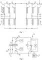
- Fig. 1schematically illustrates a power converter 1.
- the exemplified power converteris a three-phase alternating current (AC) to AC converter.
- MMCmodular multilevel converter
- the present conceptcould be utilised in an MMCS of any type, or in general any type of power converter which comprises a number of identical converter cells, including redundant converter cells. Examples of such power converters are a rectifier, an inverter, a direct current (DC) to DC converter or an uninterruptable power supply (UPS).
- the present conceptcould also be utilised with power converters arranged to handle fewer or more electrical phases than the exemplified three phases.
- the exemplified power converter 1comprises a plurality of legs L1-L3 on an input terminal side 3 of the power converter 1, and a plurality of legs L4-L6 on an output terminal side 5 of the power converter 1.
- Each leg Li-L6comprises a plurality of identical converter cells 7.
- Each converter cell 7comprises semiconductor switching modules and a cell capacitor. The converter cells are utilised to enable the power converter to convert the input voltage of each electrical phase to a desired output voltage and/or frequency of a corresponding electrical phase.
- the operation of power convertersis well-known, and will not be described in more detail herein.
- Fig. 2shows an example of a converter cell 7-1 and an arrangement 6 for determining the degradation of a cell capacitor.
- the arrangement 6comprises a processor 6a and is provided with a computer program comprising computer-executable components which when run on the processor 6a, performs the steps of the method(s) for determining a capacitor degradation parameter associated with the degradation of a cell capacitor as presented herein.
- the converter cell 7-1is of half-bridge type, and comprises a plurality of semiconductor switching modules 9a, 9b.
- Each semiconductor switching module 9a, 9bcomprises a semiconductor switch and a diode connected in anti-parallel with the semiconductor switch.
- the semiconductor switching modulemay for example be of IGBT type or of gate-controlled thyristor type.
- the converter cell 7-1also comprises a cell capacitor, or dc-link capacitor, C connected between the collector of the semiconductor switching module 9a and the emitter of the other semiconductor switching module 9b.
- the converter cell 7-1has one terminal 13, according to the example in Fig. 2a the DC side, between the emitter of the upper semiconductor switching module 9a and the collector of the lower semiconductor switching module 9b.
- the other terminal 11, according to the example the AC side,is at the emitter of the lower semiconductor switching module 9b.
- lower and upperis here merely meant the placement of the semiconductor switching modules as shown in Fig. 2 .
- the converter cell 7-1comprises a gate unit 11a connected to the gate of the semiconductor switching module 9a to control the switching of that semiconductor switching module, and a gate unit 11b connected to the gate of the semiconductor switching device 9b to control the switching of that semiconductor switching module.
- the gate unitshence control the gate voltage to the semiconductor switching modules. Normal operation of converter cells is well-known in the art, and will not be discussed any further herein.
- the converter cell 7-1may comprise a cell resistor R, such as a balancing resistor and/or discharge resistor. The magnitude of such a cell resistor R is known.
- the cell resistor Rmay be used for limiting the discharge current when the cell capacitor C is being discharged.
- the converter cell 7-1comprises an auxiliary power supply 8 arranged to power the gate units 11a, 11b.
- the auxiliary power supplyis arranged to consume a constant amount of power.
- the cell convertercomprises both the resistor and the auxiliary power supply, as schematically shown in both Figure 2 and Figure 3 .
- the arrangement 6, especially the processor 6ais arranged to obtain a measurement parameter value associated with the discharging of the cell capacitor C from a measurement start voltage level at a measurement start time to a measurement end voltage level at a measurement end time, and based on the measurement parameter value to determine a capacitor degradation parameter value associated with the degree of degradation of the cell capacitor C.
- the capacitor degradation parametermay for example be a measure of the capacitance of the cell capacitor C, or a ratio which relates the current capacitance of the cell capacitor to a reference capacitance of the cell capacitor, corresponding to the capacitance of a new cell capacitor.
- the measurement parameter valuemay be the discharge time, i.e. time difference between the measurement start time and the measurement end time, from the measurement start voltage level to the measurement end voltage level, or the measurement end voltage level in case the discharge time is predetermined.
- the arrangement 6may for example be a local converter cell controller arranged to control only the operation of the converter cell, e.g. switching of the semiconductor switching modules 9a, 9b, or a supervisory power converter controller arranged to provide supervisory control of the entire power converter.
- Fig. 3depicts another example of a converter cell for which the degradation of the cell capacitor may be determined.
- the converter cell 7-2is of full-bridge type and comprises a plurality of semiconductor switching modules 9a-9d, and a cell capacitor C.
- the converter cell 7-2comprises gate units 11a-11d, each being arranged to control the gate voltage of the gate of a respective semiconductor switching module 9a-9d.
- the converter cell 7-2may have a bypass switch 15 for bypassing thereof.
- the arrangement 6is identical to the arrangement presented in Fig. 2 , and is thus arranged to determine the degree of degradation of the cell capacitor C of the converter cell 7-2.
- the arrangement 6is connected to the terminals of the cell capacitor C, it should be noted that these only illustrate that the arrangement 6 in some sense is connected to the terminals of the cell capacitor. This could be directly in case the arrangement is a local converter cell controller, or indirectly via a local converter cell controller in case the arrangement is a supervisory converter cell controller. It is also contemplated that this connection could be a wireless connection via for example the local converter cell controller to a supervisory power converter controller.
- the method(s) of determining the capacitor degradation parameter associated with the degree of degradation of the cell capacitorutilises the fact that there are a number of identical converter cells 7-1 or 7-2 in the power converter 1, including redundant converter cells.
- the converter cell that is to be subject to a measurement for determining the value of the capacitor degradation parameter associated with the degree of degradation of the cell capacitorcan be a converter cell which is normally active.
- the corresponding converter cellis first set in a bypass mode, and the power converter continues operation with the remaining cells. At this point, the degree of degradation of the cell capacitor can be determined in the bypassed converter cell.
- the bypass operationmay be performed in several manners.
- the converter cellmay for example be provided with a bypass switch, such as switch 15 of the converter cell 7-1.
- a bypass switchsuch as switch 15 of the converter cell 7-1.
- the switch 15When the switch 15 is set in a closed state, the converter cell 7-1 is bypassed, i.e. the current flows through the switch 15 instead of through the semiconductor switching modules 9a and 9b. In this bypassed state, the cell capacitor is not charged, and the determination of the capacitor degradation may be performed.
- Another way to bypass the converter cell 7-1would be to set the lower semiconductor switching module 9b, i.e. the one which has its emitter connected to a terminal of the cell capacitor C, in an ON-state and the upper semiconductor switching module 9a, i.e. the one which has its collector connected to a terminal of the cell capacitor C, in an OFF-state, while the degree of degradation of the cell capacitor C is determined.
- the full-bridge converter cell 7-2could also be either disconnected by means of a dedicated bypass switch, or by means of proper switching of the semiconductor switching modules 9a-9d.
- semiconductor switching modules 9a and 9c or semiconductor switching modules 9b and 9dmay be set in their ON-state, while the remaining semiconductor switching modules 9b and 9d or 9a and 9c, respectively, are set in the OFF-state for bypassing the converter cell 7-2.
- the supervisory power converter controlleradministers the converter cells in a power converter.
- the supervisory power converter controllermay thus, for example, itself set the cell converter to be bypassed, or it may instruct the local converter cell controller to set the converter cell in bypass mode.
- the supervisory power converter controllermay provide for a redundant converter cell to be set into an active state to become an active converter cell while the previously active converter cell is subjected to the cell capacitor degradation determination.
- the converter cellmay be reactivated and it is communicated to the supervisory power converter controller that the converter cell may be operated again.
- the supervisory power converter controllermay bring the dc-link voltage of the converter cell back to nominal voltage.
- the determination of the value of the capacitor degradation parameteris based on the a measurement parameter value which is associated with the discharging of the cell capacitor C from the measurement start voltage level at a measurement start time, at which the measurement start voltage level is across the dc-link formed by the cell capacitor C, and a measurement end voltage level at a measurement end time at which the measurement end voltage level is across the dc-link.
- the measurement start voltage levelis preferably below the nominal dc-link voltage such that the dc-link voltage ripple has no influence on the measurement process.
- the nominal dc-link voltage levelis the voltage level across the dc-link when the converter cell is in operation.
- the measurement end voltage levelis preferably above the converter cell undervoltage protection level.
- the measurement start voltage level and the measurement end voltage levelare according to one variation predetermined voltage levels, while according to another variation the measurement start time, the starting voltage and the measurement end time are predetermined.
- the former caseit is known at what voltage levels the measurement start time and the measurement end time are to be registered.
- the latter caseit is known at what time, i.e. the measurement end time, a measurement end voltage is to be measured.
- the measurement parameter valuemay thus be the time difference between the measurement start time and the measurement end time, or alternatively, the measurement end voltage level measured after a predetermined time has elapsed from the measurement start time. I the latter case, both the measurement start time, associated with a predetermined measurement start voltage level, and the measurement end time are hence predetermined.
- a step a)the arrangement 6 obtains the measurement parameter value which is associated with the discharging of the cell capacitor C from a measurement start voltage level at a measurement start time to a measurement end voltage at a measurement end time.
- the measurement parameter valueis the time difference between the measurement start time and the measurement end time.
- the measurement parameter valueis the measurement end voltage level obtained or measured after a predetermined time after the measurement start time.
- a step b)the value of the capacitor degradation parameter associated with the degradation of the cell capacitor is determined based on the measurement parameter value.
- the capacitor degradation parameter whose value is determinedis directly proportional to the time difference between the measurement start time and the measurement end time.
- This capacitor degradation parametermay be the capacitance of the cell capacitor, or a ratio between the current capacitance and a reference capacitance corresponding to the capacitance of the cell capacitor when the cell capacitor was new.
- this valuemay be evaluated to determine whether the cell capacitor should be utilised in continued operation of the converter cell or if it has reached its end-of-life.
- a decrease of about 20% from the initial capacitanceis typically considered to indicate an end-of-life condition of a capacitor.
- step b)the determining of the value of the capacitor degradation parameter is further based on the measurement end voltage level. This may be the case if the measurement parameter value is the measurement end voltage level and also in the case measurement parameter is the time difference between the measurement start time and measurement end time.
- the determining of the value of the capacitor degradation parameteris further based on the measurement start voltage level.
- P auxis the power consumption of the auxiliary power supply 8
- V sis the measurement start voltage level
- V mis the measurement end voltage level
- t dis the time difference between the measurement start time and the measurement end time.
- the determination of the capacitor degradation parameter, in this case the capacitanceis hence further based on the power consumption of the auxiliary power supply.
- the capacitance of the cell capacitor Cmay be determined by the following relation.
- C⁇ 1 R ⁇ ln V m V s ⁇ t d
- the determination of the capacitor degradation parameterin this case the capacitance, is hence further based on the cell resistor R.
- the determination of the capacitor degradation parameteris hence further based on the power consumption of the auxiliary power supply and on the cell resistor R.
- the capacitor degradation parameteris a ratio between the current capacitance and the reference capacitance, and this ratio may be expressed as follows.
- C c C reft d t ref
- C refthe initial capacitance value, i.e. a reference capacitance value, when the cell capacitor was new
- t refis a reference time difference for discharging the capacitor from the measurement start voltage level to the measurement end voltage level when the cell capacitor was new, i.e. when it had the reference capacitance C ref .
- the ratio between the current time difference and the reference time differencemay be determined.
- the ratiowill be a number between 0 and 1, and if the ratio is 0.8 or below, for example, the cell capacitor end-of-life condition has been reached. It should be noted that as an alternative the ratio could be inverted such that the current time difference is the denominator and the reference time difference is the numerator.
- the temperature of the cell capacitor Cis also obtained and taken into account.
- the time differencemay be associated with a specific cell capacitor temperature.
- This temperaturemay be compared to a reference cell capacitor temperature that was present at the time of the reference measurement. This information may be used to determine the reliability/validity of the determination of the value of the capacitor degradation parameter.
- the temperature of the cell capacitormay be determined for example by means of one or more sensor(s) located in the converter cell, e.g. heat sink or ambient temperature sensors, or by estimation by means of thermal models.
- the local converter cell controllermay obtain measurements of the measurement start voltage level via a voltage sensor and register the time, i.e. measurement start time, at which the measurement start voltage level was measured. Moreover, the local converter cell controller may obtain measurements of the measurement end voltage level via a voltage sensor and register the time, i.e. the measurement end time, at which the measurement end voltage level was measured. The measurement start time and the measurement end time may then be sent to the supervisory power converter controller, which may determine the value of the capacitor degradation parameter associated with the degree of degradation based on the measurement start time and the measurement end time.
- the local converter cell controllercould also determine the time difference between the measurement start time and measurement end time end send the time difference to the supervisory power converter controller, for it to determine the value of the capacitor degradation parameter.
- the local converter cell controllermay determine the measurement end voltage level and send the measurement end voltage level to the supervisory power converter controller for it to determine the value of the capacitor degradation parameter based on the measured measurement end voltage, i.e. in variations in which the time difference is predetermined but the measurement end voltage level at the measurement end time is unknown prior to measurement.
- the time differencemay be obtained by the local converter cell controller, after the voltage measurements have been carried out and the local converter cell controller is arranged to determine the value of the capacitor degradation parameter.
- the measurement end voltage levelmay be obtained by the local converter cell controller in case the time difference between the measurement start time and the measurement end time is predetermined, wherein the local converter cell controller may determine the value of the capacitor degradation parameter based on the measurement end voltage level.
- the determined value of the capacitor degradation parametermay be sent to the supervisory power converter controller, which may store such values of the capacitor degradation parameter for all converter cells of the power converter.
- the methods and arrangements presented hereinmay be utilised to determine the degree of degradation of essentially any type of capacitor in a converter cell, for example electrolytic capacitors and film capacitors.
- subsea applicationssuch as for powering pumps and compressors in subsea installations, or for subsea HVDC/HVAC power transmission and power distribution systems, as well as offshore power generation such as wind energy, tidal energy, wave energy, and ocean current energy.
Landscapes
- Engineering & Computer Science (AREA)
- Power Engineering (AREA)
- Physics & Mathematics (AREA)
- General Physics & Mathematics (AREA)
- Inverter Devices (AREA)
Description
- The present disclosure generally relates to power converters comprising converter cells which include semiconductor switching modules and a cell capacitor. In particular, it relates to a method and to an arrangement for determining cell capacitor degradation in a converter cell.
- In many applications, high reliability of power converters is required. In voltage source converters, the capacitor bank, in the following referred to as cell capacitor, is one of the major parts causing failures of the power converter because the often implemented electrolytic capacitors have only a limited lifetime.
- Especially in modular multilevel converters (MMC), aging of the cell capacitors is a particular problem as the capacitors are subject to high currents at multiples of the fundamental and at the switching frequency, leading to early aging and capacitance drop. As such modular multilevel converters are designed for high reliability, health monitoring of the cell capacitor is of major importance.
- During the aging process of electrolytic capacitors, the capacitance drops continuously and the equivalent series resistance (ESR) increases. Many manufacturers define the end-of-life of their capacitors if the initial capacitance has dropped by 20% and/or the ESR has increased by 200-300%.
US2010/0321038 discloses a device for monitoring the aging of the capacitors in a power converter comprising a number of converter cells, by means of capacitance measurement. For each phase module a branch current sensor for detecting a phase module branch current is provided. Furthermore, for each submodule there exists a submodule sensor for detecting a capacitor voltage dropped across the capacitor, means for detecting the switching states of the submodule, and an evaluation unit for determining the capacitance of the capacitors of each phase module. The determining of the capacitance is dependent on the integration of the measured phase module branch current, the switching state or states and the capacitor voltage. This yields the charge change of the capacitors. The capacitance of each capacitor results from the division of the charge change with the voltage change. The charge and voltage are detected between the turn-on and turn-off instants of the submodule.- The above-described method relies on both current and voltage measurements, and especially on computations such as integration of the detected branch currents in order to determine the capacitance.
- An object of the present disclosure is to provide a method and an arrangement which enables simple and reliable cell capacitor degradation determination when the power converter is in an online state.
- Hence, according to a first aspect of the present disclosure there is provided a method of determining a capacitor degradation parameter associated with the degree of degradation of a cell capacitor in a converter cell of a power converter comprising a plurality of identical converter cells, including redundant converter cells, which converter cell, prior to determining the capacitor degradation parameter, has been bypassed, wherein the method comprises:
- a) obtaining a measurement parameter value associated with discharging of the cell capacitor, forming a dc-link, from a measurement start voltage level at a measurement start time to a measurement end voltage level at a measurement end time, and
determining a value of the capacitor degradation parameter based on the measurement parameter value - An effect which may be obtainable thereby is that a value of the capacitor degradation parameter may be determined in a simple manner, because the method relies on large voltage differences instead of small voltage variations on top of a high dc-link voltage, without having to set the power converter in an offline mode. Due to a voltage swing used for the measurement is relatively large, in some applications in the order of 100 V, sensitivity to for example noise is greatly enhanced and problems with the measurement resolution are reduced as A/D converter resolution normally limits the measurement of small voltage ripples on top of e.g. a 1000 V dc-link voltage.
- By means of redundancy, the degradation level of the cell capacitor in any converter cell in the power converter may be determined while the power converter is in operation. For this purpose, the converter cell that is to be subjected to the cell capacitor degradation measurement is bypassed, wherein the cell capacitor degradation may be performed by simple time measurements at two voltages, namely the starting voltage and the measurement end voltage, or by measuring the measurement end voltage if the time difference between a predetermined starting voltage and the measurement end voltage, which in this case is unknown, is predetermined.
- According to one embodiment the measurement start voltage level and the measurement end voltage level are predetermined, and wherein the measurement parameter value is a time difference between the measurement start time and the measurement end time.
- According to one embodiment measurement start time and measurement end time are predetermined and the measurement parameter value is the measurement end voltage.
- According to one embodiment the measurement start voltage level is below a nominal dc-link voltage level, the nominal dc-link voltage level being the voltage level across the dc-link when the converter cell is in operation.
- According to one embodiment the measurement end voltage level is above a converter cell undervoltage protection level.
- According to one embodiment in step b) the determining of the value of the capacitor degradation parameter is further based on the measurement start voltage level and the measurement end voltage level.
- According to one embodiment the capacitor degradation parameter value is the capacitance of the cell capacitor.
- According to one embodiment step b) is further based on a cell resistor value.
- According to one embodiment the determining in step b) is further based on a power consumption of an auxiliary power supply of the converter cell.
- According to one embodiment the determining in step b) comprises determining a ratio between the time difference and a reference time difference indicative of the discharge time from the starting voltage to the measurement end voltage of a new cell capacitor. Thereby, it is not necessary to determine or know the current capacitance nor the reference capacitance, nor the resistor value, nor the power consumption of the auxiliary power supply. By means of the ratio between only the two time differences, a measure of the cell capacitor degradation may be obtained.
- One embodiment comprises obtaining a current temperature of the cell capacitor and comparing the current temperature with a reference temperature to determine the reliability of determining the capacitor degradation parameter.
- According to a second aspect of the present disclosure there is provided a power converter comprising a plurality of identical converter cells, each converter cell comprising a cell capacitor, and each converter cell being arranged to be bypassed, the power converter further comprising a processor for determining a capacitor degradation parameter associated with the degree of degradation of a cell capacitor, the processor being arranged to obtain a measurement parameter value associated with discharging of the cell capacitor from a measurement start voltage level at a measurement start time to a measurement end voltage level at a measurement end time when the converter cell is bypassed, and to determine a value of the capacitor degradation parameter based on the measurement parameter value. According to one embodiment the measurement start voltage level and the measurement end voltage level are predetermined, and wherein the measurement parameter value is a time difference between the measurement start time and the measurement end time.
- According to one embodiment the measurement start time and measurement end time are predetermined and the measurement parameter value is the measurement end voltage.
- According to one embodiment the processor is arranged to determine the value of the capacitor degradation parameter by means of a ratio between the time difference and a reference time difference indicative of the discharge time from the starting voltage to the measurement end voltage of a new cell capacitor.
- According to one embodiment the processor is arranged in a local converter cell controller or a supervisory power converter controller.
- The specific embodiments of the inventive concept will now be described, by way of example, with reference to the accompanying drawings, in which:
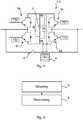
Fig. 1 schematically depicts an example of a power converter comprising a plurality of converter cells;Fig. 2 depicts an example of a half-bridge converter cell and an arrangement for determining the degree of degradation of the cell capacitor;Fig. 3 depicts an example of a full-bridge converter cell and an arrangement for determining the degree of degradation of the cell capacitor; andFig. 4 is a flowchart of a method of determining a capacitor degradation parameter associated with the degradation of a cell capacitor in a converter cell of a power converter.- The inventive concept will now be described more fully hereinafter with reference to the accompanying drawings, in which exemplifying embodiments are shown. The inventive concept may, however, be embodied in many different forms and should not be construed as limited to the embodiments set forth herein; rather, these embodiments are provided by way of example so that this disclosure will be thorough and complete, and will fully convey the scope of the inventive concept to those skilled in the art. Like numbers refer to like elements throughout the description.
Fig. 1 schematically illustrates apower converter 1. The exemplified power converter is a three-phase alternating current (AC) to AC converter. Especially, it is a modular multilevel converter (MMC). It should be noted that the present concept could be utilised in an MMCS of any type, or in general any type of power converter which comprises a number of identical converter cells, including redundant converter cells. Examples of such power converters are a rectifier, an inverter, a direct current (DC) to DC converter or an uninterruptable power supply (UPS). The present concept could also be utilised with power converters arranged to handle fewer or more electrical phases than the exemplified three phases.- The
exemplified power converter 1 comprises a plurality of legs L1-L3 on aninput terminal side 3 of thepower converter 1, and a plurality of legs L4-L6 on an output terminal side 5 of thepower converter 1. Each leg Li-L6 comprises a plurality of identical converter cells 7. Each converter cell 7 comprises semiconductor switching modules and a cell capacitor. The converter cells are utilised to enable the power converter to convert the input voltage of each electrical phase to a desired output voltage and/or frequency of a corresponding electrical phase. The operation of power converters is well-known, and will not be described in more detail herein. Fig. 2 shows an example of a converter cell 7-1 and anarrangement 6 for determining the degradation of a cell capacitor. Thearrangement 6 comprises aprocessor 6a and is provided with a computer program comprising computer-executable components which when run on theprocessor 6a, performs the steps of the method(s) for determining a capacitor degradation parameter associated with the degradation of a cell capacitor as presented herein.- The converter cell 7-1 is of half-bridge type, and comprises a plurality of
semiconductor switching modules semiconductor switching module - The converter cell 7-1 also comprises a cell capacitor, or dc-link capacitor, C connected between the collector of the
semiconductor switching module 9a and the emitter of the othersemiconductor switching module 9b. The converter cell 7-1 has one terminal 13, according to the example inFig. 2a the DC side, between the emitter of the uppersemiconductor switching module 9a and the collector of the lowersemiconductor switching module 9b. Theother terminal 11, according to the example the AC side, is at the emitter of the lowersemiconductor switching module 9b. With the terms lower and upper is here merely meant the placement of the semiconductor switching modules as shown inFig. 2 . - The converter cell 7-1 comprises a
gate unit 11a connected to the gate of thesemiconductor switching module 9a to control the switching of that semiconductor switching module, and agate unit 11b connected to the gate of thesemiconductor switching device 9b to control the switching of that semiconductor switching module. The gate units hence control the gate voltage to the semiconductor switching modules. Normal operation of converter cells is well-known in the art, and will not be discussed any further herein. - According to one variation, the converter cell 7-1 may comprise a cell resistor R, such as a balancing resistor and/or discharge resistor. The magnitude of such a cell resistor R is known. The cell resistor R may be used for limiting the discharge current when the cell capacitor C is being discharged. According to one variation the converter cell 7-1 comprises an
auxiliary power supply 8 arranged to power thegate units Figure 2 andFigure 3 . - The
arrangement 6, especially theprocessor 6a, is arranged to obtain a measurement parameter value associated with the discharging of the cell capacitor C from a measurement start voltage level at a measurement start time to a measurement end voltage level at a measurement end time, and based on the measurement parameter value to determine a capacitor degradation parameter value associated with the degree of degradation of the cell capacitor C. The capacitor degradation parameter may for example be a measure of the capacitance of the cell capacitor C, or a ratio which relates the current capacitance of the cell capacitor to a reference capacitance of the cell capacitor, corresponding to the capacitance of a new cell capacitor. The measurement parameter value may be the discharge time, i.e. time difference between the measurement start time and the measurement end time, from the measurement start voltage level to the measurement end voltage level, or the measurement end voltage level in case the discharge time is predetermined. - The
arrangement 6 may for example be a local converter cell controller arranged to control only the operation of the converter cell, e.g. switching of thesemiconductor switching modules Fig. 3 depicts another example of a converter cell for which the degradation of the cell capacitor may be determined. The converter cell 7-2 is of full-bridge type and comprises a plurality ofsemiconductor switching modules 9a-9d, and a cell capacitor C. The converter cell 7-2 comprisesgate units 11a-11d, each being arranged to control the gate voltage of the gate of a respectivesemiconductor switching module 9a-9d. The converter cell 7-2 may have abypass switch 15 for bypassing thereof.- The
arrangement 6 is identical to the arrangement presented inFig. 2 , and is thus arranged to determine the degree of degradation of the cell capacitor C of the converter cell 7-2. - Although in
Figs 2 and3 , thearrangement 6 is connected to the terminals of the cell capacitor C, it should be noted that these only illustrate that thearrangement 6 in some sense is connected to the terminals of the cell capacitor. This could be directly in case the arrangement is a local converter cell controller, or indirectly via a local converter cell controller in case the arrangement is a supervisory converter cell controller. It is also contemplated that this connection could be a wireless connection via for example the local converter cell controller to a supervisory power converter controller. - The operation of several examples of determining a capacitor degradation parameter associated with the degradation of a cell capacitor will now be described with reference to
Fig 4 . - In short, the method(s) of determining the capacitor degradation parameter associated with the degree of degradation of the cell capacitor utilises the fact that there are a number of identical converter cells 7-1 or 7-2 in the
power converter 1, including redundant converter cells. The converter cell that is to be subject to a measurement for determining the value of the capacitor degradation parameter associated with the degree of degradation of the cell capacitor can be a converter cell which is normally active. The corresponding converter cell is first set in a bypass mode, and the power converter continues operation with the remaining cells. At this point, the degree of degradation of the cell capacitor can be determined in the bypassed converter cell. - The bypass operation may be performed in several manners. The converter cell may for example be provided with a bypass switch, such as
switch 15 of the converter cell 7-1. When theswitch 15 is set in a closed state, the converter cell 7-1 is bypassed, i.e. the current flows through theswitch 15 instead of through thesemiconductor switching modules - Another way to bypass the converter cell 7-1 would be to set the lower
semiconductor switching module 9b, i.e. the one which has its emitter connected to a terminal of the cell capacitor C, in an ON-state and the uppersemiconductor switching module 9a, i.e. the one which has its collector connected to a terminal of the cell capacitor C, in an OFF-state, while the degree of degradation of the cell capacitor C is determined. The full-bridge converter cell 7-2 could also be either disconnected by means of a dedicated bypass switch, or by means of proper switching of thesemiconductor switching modules 9a-9d. In the latter case,semiconductor switching modules semiconductor switching modules semiconductor switching modules - Typically, the supervisory power converter controller administers the converter cells in a power converter. The supervisory power converter controller may thus, for example, itself set the cell converter to be bypassed, or it may instruct the local converter cell controller to set the converter cell in bypass mode. Moreover, the supervisory power converter controller may provide for a redundant converter cell to be set into an active state to become an active converter cell while the previously active converter cell is subjected to the cell capacitor degradation determination.
- After the monitoring process is finished, the converter cell may be reactivated and it is communicated to the supervisory power converter controller that the converter cell may be operated again. The supervisory power converter controller may bring the dc-link voltage of the converter cell back to nominal voltage.
- As briefly mentioned above, the determination of the value of the capacitor degradation parameter is based on the a measurement parameter value which is associated with the discharging of the cell capacitor C from the measurement start voltage level at a measurement start time, at which the measurement start voltage level is across the dc-link formed by the cell capacitor C, and a measurement end voltage level at a measurement end time at which the measurement end voltage level is across the dc-link. The measurement start voltage level is preferably below the nominal dc-link voltage such that the dc-link voltage ripple has no influence on the measurement process. The nominal dc-link voltage level is the voltage level across the dc-link when the converter cell is in operation. The measurement end voltage level is preferably above the converter cell undervoltage protection level. The measurement start voltage level and the measurement end voltage level are according to one variation predetermined voltage levels, while according to another variation the measurement start time, the starting voltage and the measurement end time are predetermined. In the former case, it is known at what voltage levels the measurement start time and the measurement end time are to be registered. In the latter case it is known at what time, i.e. the measurement end time, a measurement end voltage is to be measured.
- The measurement parameter value may thus be the time difference between the measurement start time and the measurement end time, or alternatively, the measurement end voltage level measured after a predetermined time has elapsed from the measurement start time. I the latter case, both the measurement start time, associated with a predetermined measurement start voltage level, and the measurement end time are hence predetermined.
- In a step a) the
arrangement 6 obtains the measurement parameter value which is associated with the discharging of the cell capacitor C from a measurement start voltage level at a measurement start time to a measurement end voltage at a measurement end time. - As mentioned above, according to one variation the measurement parameter value is the time difference between the measurement start time and the measurement end time. According to another variation, the measurement parameter value is the measurement end voltage level obtained or measured after a predetermined time after the measurement start time.
- In a step b) the value of the capacitor degradation parameter associated with the degradation of the cell capacitor is determined based on the measurement parameter value.
- The capacitor degradation parameter whose value is determined is directly proportional to the time difference between the measurement start time and the measurement end time. This capacitor degradation parameter may be the capacitance of the cell capacitor, or a ratio between the current capacitance and a reference capacitance corresponding to the capacitance of the cell capacitor when the cell capacitor was new.
- When the value of the capacitor degradation parameter has been obtained, this value may be evaluated to determine whether the cell capacitor should be utilised in continued operation of the converter cell or if it has reached its end-of-life. A decrease of about 20% from the initial capacitance is typically considered to indicate an end-of-life condition of a capacitor.
- According to one variation of the method, in step b) the determining of the value of the capacitor degradation parameter is further based on the measurement end voltage level. This may be the case if the measurement parameter value is the measurement end voltage level and also in the case measurement parameter is the time difference between the measurement start time and measurement end time.
- According to one variation the determining of the value of the capacitor degradation parameter is further based on the measurement start voltage level.
- In case the converter cell comprises the
auxiliary power supply 8 but not the cell resistor R, the capacitance of the cell capacitor C can be determined by
auxiliary power supply 8, Vs is the measurement start voltage level, Vm is the measurement end voltage level and td is the time difference between the measurement start time and the measurement end time. The determination of the capacitor degradation parameter, in this case the capacitance, is hence further based on the power consumption of the auxiliary power supply. - In case the converter cell comprises the cell resistor R but not the
auxiliary power supply 8, the capacitance of the cell capacitor C may be determined by the following relation.
- The determination of the capacitor degradation parameter, in this case the capacitance, is hence further based on the cell resistor R.
- In variations comprising both the cell resistor R and the
auxiliary power supply 8, the capacitance of the cell capacitor C may be determined by
- The determination of the capacitor degradation parameter, in this case the capacitance, is hence further based on the power consumption of the auxiliary power supply and on the cell resistor R.
- According to one variation of the method, it is not necessary to determine the capacitance of the cell capacitor C to obtain the value of the capacitor degradation parameter. In this variation, the capacitor degradation parameter is a ratio between the current capacitance and the reference capacitance, and this ratio may be expressed as follows.

- According to one variation of the method, the temperature of the cell capacitor C is also obtained and taken into account. In this case the time difference may be associated with a specific cell capacitor temperature. This temperature may be compared to a reference cell capacitor temperature that was present at the time of the reference measurement. This information may be used to determine the reliability/validity of the determination of the value of the capacitor degradation parameter. The temperature of the cell capacitor may be determined for example by means of one or more sensor(s) located in the converter cell, e.g. heat sink or ambient temperature sensors, or by estimation by means of thermal models.
- In case the
arrangement 6 is the supervisory power converter controller, the local converter cell controller may obtain measurements of the measurement start voltage level via a voltage sensor and register the time, i.e. measurement start time, at which the measurement start voltage level was measured. Moreover, the local converter cell controller may obtain measurements of the measurement end voltage level via a voltage sensor and register the time, i.e. the measurement end time, at which the measurement end voltage level was measured. The measurement start time and the measurement end time may then be sent to the supervisory power converter controller, which may determine the value of the capacitor degradation parameter associated with the degree of degradation based on the measurement start time and the measurement end time. Alternatively, the local converter cell controller could also determine the time difference between the measurement start time and measurement end time end send the time difference to the supervisory power converter controller, for it to determine the value of the capacitor degradation parameter. According to one variation the local converter cell controller may determine the measurement end voltage level and send the measurement end voltage level to the supervisory power converter controller for it to determine the value of the capacitor degradation parameter based on the measured measurement end voltage, i.e. in variations in which the time difference is predetermined but the measurement end voltage level at the measurement end time is unknown prior to measurement. - Alternatively, if the
arrangement 6 is the local converter cell controller, the time difference may be obtained by the local converter cell controller, after the voltage measurements have been carried out and the local converter cell controller is arranged to determine the value of the capacitor degradation parameter. Alternatively, the measurement end voltage level may be obtained by the local converter cell controller in case the time difference between the measurement start time and the measurement end time is predetermined, wherein the local converter cell controller may determine the value of the capacitor degradation parameter based on the measurement end voltage level. The determined value of the capacitor degradation parameter may be sent to the supervisory power converter controller, which may store such values of the capacitor degradation parameter for all converter cells of the power converter. - It is to be noted that the method(s) presented herein could be utilised to determine the degree of degradation of the cell capacitor also in the start-up phase of the power converter after passive precharge or in idle mode.
- The methods and arrangements presented herein may be utilised to determine the degree of degradation of essentially any type of capacitor in a converter cell, for example electrolytic capacitors and film capacitors.
- It is envisaged that the methods and arrangements presented herein may be utilised in high-reliability applications, for example subsea applications, such as for powering pumps and compressors in subsea installations, or for subsea HVDC/HVAC power transmission and power distribution systems, as well as offshore power generation such as wind energy, tidal energy, wave energy, and ocean current energy.


Claims (10)
- A method of determining a capacitor degradation parameter associated with the degree of degradation of a cell capacitor (C) in a converter cell (7; 7-1; 7-2) of a power converter (1) comprising a plurality of identical converter cells (7; 7-1; 7-2), including redundant converter cells, which converter cell (7; 7-1; 7-2), prior to determining the capacitor degradation parameter, has been bypassed (7; 7-1; 7-2), wherein the capacitor degradation parameter is the capacitance of the cell capacitor (C), and wherein the method comprises:a) obtaining a measurement parameter value associated with discharging of the cell capacitor, forming a dc-link, from a measurement start voltage level at a measurement start time to a measurement end voltage level at a measurement end time,
wherein the measurement start voltage level and the measurement end voltage level are predetermined, wherein the measurement parameter value is a time difference between the measurement start time and the measurement end time or wherein measurement start time and measurement end time are predetermined and the measurement parameter value is the measurement end voltage, andb) determining a value of the capacitor degradation parameter based on a time difference between the measurement start time and the measurement end time, wherein the determining of the value of the capacitor degradation parameter is further based on the measurement start voltage level and the measurement end voltage level, wherein the capacitor degradation parameter is directly proportional to the time difference between the measurement start time and the measurement end time. - The method as claimed in claim any of the preceding claims, wherein the measurement start voltage level is below a nominal dc-link voltage level, the nominal dc-link voltage level being the voltage level across the dc-link when the converter cell is in operation.
- The method as claimed in any of the preceding claims, wherein the measurement end voltage level is above a converter cell undervoltage protection level.
- The method as claimed in any of claims the preceding claims, wherein the determining in step b) is further based on a cell resistor (R) value.
- The method as claimed in any of the preceding claims, wherein the determining in step b) is further based on a power consumption of an auxiliary power supply of the converter cell (7; 7-1; 7-2).
- The method as claimed in any of the preceding claims, comprising obtaining a current temperature of the cell capacitor (C) and comparing the current temperature with a reference temperature to determine the reliability of determining the capacitor degradation parameter.
- A method of determining a capacitor degradation parameter associated with the degree of degradation of a cell capacitor (C) in a converter cell (7; 7-1; 7-2) of a power converter (1) comprising a plurality of identical converter cells (7; 7-1; 7-2), including redundant converter cells, which converter cell (7; 7-1; 7-2), prior to determining the capacitor degradation parameter, has been bypassed (7; 7-1; 7-2), wherein the method comprises:a) obtaining a measurement parameter value associated with discharging of the cell capacitor, forming a dc-link, from a measurement start voltage level at a measurement start time to a measurement end voltage level at a measurement end time, wherein the measurement start voltage level and the measurement end voltage level are predetermined, and wherein the measurement parameter value is a time difference between the measurement start time and the measurement end time, andb) determining a value of the capacitor degradation parameter based on the measurement parameter value,wherein step b) comprises determining a ratio between the time difference and a reference time difference indicative of the discharge time from the starting voltage to the measurement end voltage of a new cell capacitor, wherein the capacitor degradation parameter is the ratio between the time difference and the reference time difference.
- A power converter (1) comprising a plurality of identical converter cells (7; 7-1; 7-2), each converter cell comprising a cell capacitor (C), and each converter cell (7; 7-1; 7-2) being arranged to be bypassed, the power converter further comprising a processor (6a) for determining a capacitor degradation parameter associated with the degree of degradation of a cell capacitor, wherein the capacitor degradation parameter is the capacitance of the cell capacitor (C), the processor being arranged to obtain a measurement parameter value associated with discharging of the cell capacitor from a measurement start voltage level at a measurement start time to a measurement end voltage level at a measurement end time when the converter cell (7; 7-1; 7-2) is bypassed,
wherein the measurement start voltage level and the measurement end voltage level are predetermined, wherein the measurement parameter value is a time difference between the measurement start time and the measurement end time or wherein the measurement start time and measurement end time are predetermined, wherein the measurement parameter value is the measurement end voltage,
wherein the processor is arranged to determine a value of the capacitor degradation parameter based on a time difference between the measurement start time and the measurement end time, the measurement start voltage level and the measurement end voltage level, wherein the capacitor degradation parameter is directly proportional to the time difference between the measurement start time and the measurement end time. - The power converter (1) as claimed in claim 8, wherein the processor is arranged in a local converter cell controller or a supervisory power converter controller.
- A power converter (1) comprising a plurality of identical converter cells (7; 7-1; 7-2), each converter cell comprising a cell capacitor (C), and each converter cell (7; 7-1; 7-2) being arranged to be bypassed, the power converter further comprising a processor (6a) for determining a capacitor degradation parameter associated with the degree of degradation of a cell capacitor, the processor being arranged to obtain a measurement parameter value associated with discharging of the cell capacitor from a measurement start voltage level at a measurement start time to a measurement end voltage level at a measurement end time when the converter cell (7; 7-1; 7-2) is bypassed, and to determine a value of the capacitor degradation parameter based on the measurement parameter value, wherein the measurement start voltage level and the measurement end voltage level are predetermined, and wherein the measurement parameter value is a time difference between the measurement start time and the measurement end time, and wherein the processor (6a) is arranged to determine the value of the capacitor degradation parameter by means of a ratio between the time difference and a reference time difference indicative of the discharge time from the starting voltage to the measurement end voltage of a new cell capacitor, wherein the capacitor degradation parameter is a ratio between the time difference and the reference time difference.
Priority Applications (5)
| Application Number | Priority Date | Filing Date | Title |
|---|---|---|---|
| DK13198286.0TDK2887526T3 (en) | 2013-12-19 | 2013-12-19 | Method and power rectifier for determining deterioration of a cell capacitor in a converter cell |
| EP13198286.0AEP2887526B1 (en) | 2013-12-19 | 2013-12-19 | Method and power converter for determining cell capacitor degradation in a converter cell |
| PCT/EP2014/075797WO2015090892A1 (en) | 2013-12-19 | 2014-11-27 | Method and power converter for determining cell capacitor degradation in a converter cell |
| US15/100,575US9651603B2 (en) | 2013-12-19 | 2014-11-27 | Method and power converter for determining cell capacitor degradation in a converter cell |
| CN201480069254.7ACN105830326B (en) | 2013-12-19 | 2014-11-27 | Method and power converter for determining the deterioration of the cell capaciator in converter unit |
Applications Claiming Priority (1)
| Application Number | Priority Date | Filing Date | Title |
|---|---|---|---|
| EP13198286.0AEP2887526B1 (en) | 2013-12-19 | 2013-12-19 | Method and power converter for determining cell capacitor degradation in a converter cell |
Publications (2)
| Publication Number | Publication Date |
|---|---|
| EP2887526A1 EP2887526A1 (en) | 2015-06-24 |
| EP2887526B1true EP2887526B1 (en) | 2019-04-03 |
Family
ID=49886687
Family Applications (1)
| Application Number | Title | Priority Date | Filing Date |
|---|---|---|---|
| EP13198286.0AActiveEP2887526B1 (en) | 2013-12-19 | 2013-12-19 | Method and power converter for determining cell capacitor degradation in a converter cell |
Country Status (5)
| Country | Link |
|---|---|
| US (1) | US9651603B2 (en) |
| EP (1) | EP2887526B1 (en) |
| CN (1) | CN105830326B (en) |
| DK (1) | DK2887526T3 (en) |
| WO (1) | WO2015090892A1 (en) |
Families Citing this family (14)
| Publication number | Priority date | Publication date | Assignee | Title |
|---|---|---|---|---|
| DE102015210796A1 (en)* | 2015-06-12 | 2016-12-15 | Siemens Aktiengesellschaft | Power converters with parallel-connected semiconductor switches |
| CN105515353B (en)* | 2016-01-27 | 2018-06-19 | 东南大学 | The four port electric power electric transformers based on mixed type module multi-level converter |
| WO2017137088A1 (en)* | 2016-02-12 | 2017-08-17 | Abb Schweiz Ag | Converter module for hvdc power station |
| WO2018216208A1 (en)* | 2017-05-26 | 2018-11-29 | 三菱電機株式会社 | Power conversion device |
| US11121637B2 (en) | 2017-09-11 | 2021-09-14 | Mitsubishi Electric Corporation | Power conversion device and power conversion system including a power converter capable of converting between alternating-current (AC) power and direct-current (DC) power |
| DE102018200909A1 (en)* | 2018-01-22 | 2019-07-25 | Siemens Aktiengesellschaft | Method for monitoring a modular power converter |
| CN112997393B (en)* | 2018-10-09 | 2022-06-14 | Abb瑞士股份有限公司 | Method and apparatus for circuit monitoring |
| CN111505524B (en)* | 2019-01-30 | 2022-09-23 | 台达电子工业股份有限公司 | On-line monitoring method of cascade converter and applicable cascade converter |
| EP3952098A4 (en)* | 2019-04-02 | 2022-06-01 | Mitsubishi Electric Corporation | Power conversion device |
| EP3780366A1 (en)* | 2019-08-13 | 2021-02-17 | Vestas Wind Systems A/S | Dc chopper for mmc cell with integrated chopper resistor |
| WO2023023235A1 (en)* | 2021-08-20 | 2023-02-23 | Vertiv Corporation | Systems and methods for operating an uninterruptible power supply (ups) |
| US12306266B2 (en) | 2023-05-24 | 2025-05-20 | Rockwell Automation Technologies, Inc. | Measuring DC link capacitance in power conversion systems |
| JP7612946B1 (en)* | 2023-10-17 | 2025-01-14 | 株式会社Tmeic | Power Conversion Equipment |
| EP4554073A1 (en)* | 2023-11-09 | 2025-05-14 | Innomotics GmbH | Method for detecting faults in a submodule capacitor of a modular multilevel power converter |
Family Cites Families (15)
| Publication number | Priority date | Publication date | Assignee | Title |
|---|---|---|---|---|
| US4621227A (en) | 1984-02-29 | 1986-11-04 | Borg-Warner Corporation | Measuring system for determining the capacitance ratio of a pair of capacitors |
| CA2387969A1 (en) | 2000-08-30 | 2002-03-07 | General Electric Company | Computerized method and system for determining degradation of dc link capacitors |
| JP2003274566A (en)* | 2002-03-18 | 2003-09-26 | Nichicon Corp | Method of detecting abnormality of electric double-layer capacitor, and charging and discharging circuit using it |
| JP4385664B2 (en)* | 2003-07-08 | 2009-12-16 | パナソニック株式会社 | Vehicle power supply |
| FR2885416B1 (en) | 2005-05-07 | 2016-06-10 | Acam Messelectronic Gmbh | METHOD AND DEVICE FOR MEASURING CAPACITIES. |
| WO2008016050A1 (en)* | 2006-07-31 | 2008-02-07 | Mitsubishi Electric Corporation | Power supply device and sequencer system |
| WO2008067787A1 (en)* | 2006-12-08 | 2008-06-12 | Siemens Aktiengesellschaft | Monitoring of the aging of capacitors in a converter by means of capacitance measurement |
| KR100998577B1 (en) | 2007-08-29 | 2010-12-07 | 주식회사 와튼 | Aging State Diagnosis Device of Power Conversion Device and Diagnosis Method thereof |
| US7830269B2 (en) | 2007-09-14 | 2010-11-09 | Astec International Limited | Health monitoring for power converter capacitors |
| FI120280B (en) | 2008-01-21 | 2009-08-31 | Switch High Power Converters O | Method for checking the condition of capacitors in a DC voltage intermediate |
| JP5186690B2 (en)* | 2008-03-21 | 2013-04-17 | 株式会社小松製作所 | Method and apparatus for determining deterioration state of power storage device in hybrid construction machine |
| US8982591B2 (en) | 2011-10-18 | 2015-03-17 | Tigo Energy, Inc. | System and method for exchangeable capacitor modules for high power inverters and converters |
| CN102495292B (en) | 2011-11-17 | 2013-08-21 | 北京鼎汉技术股份有限公司 | Method and circuit for online monitoring capacity state of bus capacitor |
| CN202903906U (en)* | 2012-09-06 | 2013-04-24 | 漆良波 | Capacitor aging test circuit |
| CN202854258U (en)* | 2012-11-06 | 2013-04-03 | 首都师范大学 | Supercapacitor bank degradation dynamic monitoring device |
- 2013
- 2013-12-19EPEP13198286.0Apatent/EP2887526B1/enactiveActive
- 2013-12-19DKDK13198286.0Tpatent/DK2887526T3/enactive
- 2014
- 2014-11-27CNCN201480069254.7Apatent/CN105830326B/enactiveActive
- 2014-11-27USUS15/100,575patent/US9651603B2/enactiveActive
- 2014-11-27WOPCT/EP2014/075797patent/WO2015090892A1/enactiveApplication Filing
Non-Patent Citations (1)
| Title |
|---|
| None* |
Also Published As
| Publication number | Publication date |
|---|---|
| US9651603B2 (en) | 2017-05-16 |
| EP2887526A1 (en) | 2015-06-24 |
| CN105830326A (en) | 2016-08-03 |
| US20160313387A1 (en) | 2016-10-27 |
| CN105830326B (en) | 2017-07-14 |
| DK2887526T3 (en) | 2019-06-24 |
| WO2015090892A1 (en) | 2015-06-25 |
Similar Documents
| Publication | Publication Date | Title |
|---|---|---|
| EP2887526B1 (en) | Method and power converter for determining cell capacitor degradation in a converter cell | |
| EP2682769B1 (en) | Apparatus for diagnosing DC link capacitor of inverter | |
| US10063058B2 (en) | Power converter | |
| Ronanki et al. | Failure prediction of submodule capacitors in modular multilevel converter by monitoring the intrinsic capacitor voltage fluctuations | |
| US8924170B2 (en) | Method and system for detecting a failed rectifier in an AC/DC converter | |
| US11031882B2 (en) | Modular multilevel converter having capacitor degradation determination | |
| US9653984B2 (en) | Filter capacitor degradation detection apparatus and method | |
| EP3220523B1 (en) | Phase loss detection in active front end converters | |
| EP3637115B1 (en) | Method and apparatus for detecting capacitance value of filter capacitor in inverter | |
| AU2019245978B2 (en) | Power source quality management system and air conditioning apparatus | |
| Ghadrdan et al. | On-line condition monitoring system for DC-link capacitor of back-to-back converters using large-signal transients | |
| KR101806595B1 (en) | Apparatus for controlling inverter | |
| US10069438B2 (en) | Power converter with capacitor voltage balancing | |
| CN109655703A (en) | Self checking method, device, equipment and the storage medium of parallel power module | |
| EP3393033B1 (en) | Matrix converter and method for determining constants of alternating-current motor | |
| JP7347270B2 (en) | power converter | |
| CN111725992B (en) | Multiphase converter | |
| KR101171557B1 (en) | A Simple ESR Measurement System for DC Bus Capacitor Using DC/DC Converter | |
| JP2009115634A (en) | Power supply system and current measurement method for power supply system | |
| CN113924709A (en) | power supply unit | |
| JP6738263B2 (en) | Insulation resistance inspection device, power converter, and insulation resistance measuring method | |
| US20150108932A1 (en) | Apparatus for restarting medium voltage inverter | |
| KR101893240B1 (en) | Apparatus for controlling inverter | |
| Kamel et al. | Fault diagnoses for all the stages of the power electronic converter | |
| US12132384B2 (en) | Current measuring circuit for a converter, converter circuit and converter |
Legal Events
| Date | Code | Title | Description |
|---|---|---|---|
| PUAI | Public reference made under article 153(3) epc to a published international application that has entered the european phase | Free format text:ORIGINAL CODE: 0009012 | |
| 17P | Request for examination filed | Effective date:20131219 | |
| AK | Designated contracting states | Kind code of ref document:A1 Designated state(s):AL AT BE BG CH CY CZ DE DK EE ES FI FR GB GR HR HU IE IS IT LI LT LU LV MC MK MT NL NO PL PT RO RS SE SI SK SM TR | |
| AX | Request for extension of the european patent | Extension state:BA ME | |
| RBV | Designated contracting states (corrected) | Designated state(s):AL AT BE BG CH CY CZ DE DK EE ES FI FR GB GR HR HU IE IS IT LI LT LU LV MC MK MT NL NO PL PT RO RS SE SI SK SM TR | |
| RAP1 | Party data changed (applicant data changed or rights of an application transferred) | Owner name:ABB SCHWEIZ AG | |
| GRAP | Despatch of communication of intention to grant a patent | Free format text:ORIGINAL CODE: EPIDOSNIGR1 | |
| STAA | Information on the status of an ep patent application or granted ep patent | Free format text:STATUS: GRANT OF PATENT IS INTENDED | |
| INTG | Intention to grant announced | Effective date:20181119 | |
| GRAS | Grant fee paid | Free format text:ORIGINAL CODE: EPIDOSNIGR3 | |
| GRAA | (expected) grant | Free format text:ORIGINAL CODE: 0009210 | |
| STAA | Information on the status of an ep patent application or granted ep patent | Free format text:STATUS: THE PATENT HAS BEEN GRANTED | |
| AK | Designated contracting states | Kind code of ref document:B1 Designated state(s):AL AT BE BG CH CY CZ DE DK EE ES FI FR GB GR HR HU IE IS IT LI LT LU LV MC MK MT NL NO PL PT RO RS SE SI SK SM TR | |
| REG | Reference to a national code | Ref country code:GB Ref legal event code:FG4D | |
| REG | Reference to a national code | Ref country code:CH Ref legal event code:EP Ref country code:AT Ref legal event code:REF Ref document number:1116980 Country of ref document:AT Kind code of ref document:T Effective date:20190415 | |
| REG | Reference to a national code | Ref country code:DE Ref legal event code:R096 Ref document number:602013053225 Country of ref document:DE | |
| REG | Reference to a national code | Ref country code:IE Ref legal event code:FG4D | |
| REG | Reference to a national code | Ref country code:DK Ref legal event code:T3 Effective date:20190621 | |
| REG | Reference to a national code | Ref country code:NL Ref legal event code:MP Effective date:20190403 | |
| REG | Reference to a national code | Ref country code:LT Ref legal event code:MG4D | |
| REG | Reference to a national code | Ref country code:AT Ref legal event code:MK05 Ref document number:1116980 Country of ref document:AT Kind code of ref document:T Effective date:20190403 | |
| REG | Reference to a national code | Ref country code:NO Ref legal event code:T2 Effective date:20190403 | |
| PG25 | Lapsed in a contracting state [announced via postgrant information from national office to epo] | Ref country code:NL Free format text:LAPSE BECAUSE OF FAILURE TO SUBMIT A TRANSLATION OF THE DESCRIPTION OR TO PAY THE FEE WITHIN THE PRESCRIBED TIME-LIMIT Effective date:20190403 | |
| PG25 | Lapsed in a contracting state [announced via postgrant information from national office to epo] | Ref country code:HR Free format text:LAPSE BECAUSE OF FAILURE TO SUBMIT A TRANSLATION OF THE DESCRIPTION OR TO PAY THE FEE WITHIN THE PRESCRIBED TIME-LIMIT Effective date:20190403 Ref country code:LT Free format text:LAPSE BECAUSE OF FAILURE TO SUBMIT A TRANSLATION OF THE DESCRIPTION OR TO PAY THE FEE WITHIN THE PRESCRIBED TIME-LIMIT Effective date:20190403 Ref country code:CZ Free format text:LAPSE BECAUSE OF FAILURE TO SUBMIT A TRANSLATION OF THE DESCRIPTION OR TO PAY THE FEE WITHIN THE PRESCRIBED TIME-LIMIT Effective date:20190403 Ref country code:AL Free format text:LAPSE BECAUSE OF FAILURE TO SUBMIT A TRANSLATION OF THE DESCRIPTION OR TO PAY THE FEE WITHIN THE PRESCRIBED TIME-LIMIT Effective date:20190403 Ref country code:PT Free format text:LAPSE BECAUSE OF FAILURE TO SUBMIT A TRANSLATION OF THE DESCRIPTION OR TO PAY THE FEE WITHIN THE PRESCRIBED TIME-LIMIT Effective date:20190803 Ref country code:ES Free format text:LAPSE BECAUSE OF FAILURE TO SUBMIT A TRANSLATION OF THE DESCRIPTION OR TO PAY THE FEE WITHIN THE PRESCRIBED TIME-LIMIT Effective date:20190403 Ref country code:SE Free format text:LAPSE BECAUSE OF FAILURE TO SUBMIT A TRANSLATION OF THE DESCRIPTION OR TO PAY THE FEE WITHIN THE PRESCRIBED TIME-LIMIT Effective date:20190403 Ref country code:FI Free format text:LAPSE BECAUSE OF FAILURE TO SUBMIT A TRANSLATION OF THE DESCRIPTION OR TO PAY THE FEE WITHIN THE PRESCRIBED TIME-LIMIT Effective date:20190403 | |
| PG25 | Lapsed in a contracting state [announced via postgrant information from national office to epo] | Ref country code:GR Free format text:LAPSE BECAUSE OF FAILURE TO SUBMIT A TRANSLATION OF THE DESCRIPTION OR TO PAY THE FEE WITHIN THE PRESCRIBED TIME-LIMIT Effective date:20190704 Ref country code:PL Free format text:LAPSE BECAUSE OF FAILURE TO SUBMIT A TRANSLATION OF THE DESCRIPTION OR TO PAY THE FEE WITHIN THE PRESCRIBED TIME-LIMIT Effective date:20190403 Ref country code:RS Free format text:LAPSE BECAUSE OF FAILURE TO SUBMIT A TRANSLATION OF THE DESCRIPTION OR TO PAY THE FEE WITHIN THE PRESCRIBED TIME-LIMIT Effective date:20190403 Ref country code:LV Free format text:LAPSE BECAUSE OF FAILURE TO SUBMIT A TRANSLATION OF THE DESCRIPTION OR TO PAY THE FEE WITHIN THE PRESCRIBED TIME-LIMIT Effective date:20190403 Ref country code:BG Free format text:LAPSE BECAUSE OF FAILURE TO SUBMIT A TRANSLATION OF THE DESCRIPTION OR TO PAY THE FEE WITHIN THE PRESCRIBED TIME-LIMIT Effective date:20190703 | |
| PG25 | Lapsed in a contracting state [announced via postgrant information from national office to epo] | Ref country code:AT Free format text:LAPSE BECAUSE OF FAILURE TO SUBMIT A TRANSLATION OF THE DESCRIPTION OR TO PAY THE FEE WITHIN THE PRESCRIBED TIME-LIMIT Effective date:20190403 Ref country code:IS Free format text:LAPSE BECAUSE OF FAILURE TO SUBMIT A TRANSLATION OF THE DESCRIPTION OR TO PAY THE FEE WITHIN THE PRESCRIBED TIME-LIMIT Effective date:20190803 | |
| REG | Reference to a national code | Ref country code:DE Ref legal event code:R097 Ref document number:602013053225 Country of ref document:DE | |
| PG25 | Lapsed in a contracting state [announced via postgrant information from national office to epo] | Ref country code:RO Free format text:LAPSE BECAUSE OF FAILURE TO SUBMIT A TRANSLATION OF THE DESCRIPTION OR TO PAY THE FEE WITHIN THE PRESCRIBED TIME-LIMIT Effective date:20190403 Ref country code:SK Free format text:LAPSE BECAUSE OF FAILURE TO SUBMIT A TRANSLATION OF THE DESCRIPTION OR TO PAY THE FEE WITHIN THE PRESCRIBED TIME-LIMIT Effective date:20190403 Ref country code:EE Free format text:LAPSE BECAUSE OF FAILURE TO SUBMIT A TRANSLATION OF THE DESCRIPTION OR TO PAY THE FEE WITHIN THE PRESCRIBED TIME-LIMIT Effective date:20190403 | |
| PLBE | No opposition filed within time limit | Free format text:ORIGINAL CODE: 0009261 | |
| STAA | Information on the status of an ep patent application or granted ep patent | Free format text:STATUS: NO OPPOSITION FILED WITHIN TIME LIMIT | |
| PG25 | Lapsed in a contracting state [announced via postgrant information from national office to epo] | Ref country code:IT Free format text:LAPSE BECAUSE OF FAILURE TO SUBMIT A TRANSLATION OF THE DESCRIPTION OR TO PAY THE FEE WITHIN THE PRESCRIBED TIME-LIMIT Effective date:20190403 Ref country code:SM Free format text:LAPSE BECAUSE OF FAILURE TO SUBMIT A TRANSLATION OF THE DESCRIPTION OR TO PAY THE FEE WITHIN THE PRESCRIBED TIME-LIMIT Effective date:20190403 | |
| 26N | No opposition filed | Effective date:20200106 | |
| PG25 | Lapsed in a contracting state [announced via postgrant information from national office to epo] | Ref country code:TR Free format text:LAPSE BECAUSE OF FAILURE TO SUBMIT A TRANSLATION OF THE DESCRIPTION OR TO PAY THE FEE WITHIN THE PRESCRIBED TIME-LIMIT Effective date:20190403 | |
| PG25 | Lapsed in a contracting state [announced via postgrant information from national office to epo] | Ref country code:SI Free format text:LAPSE BECAUSE OF FAILURE TO SUBMIT A TRANSLATION OF THE DESCRIPTION OR TO PAY THE FEE WITHIN THE PRESCRIBED TIME-LIMIT Effective date:20190403 | |
| REG | Reference to a national code | Ref country code:CH Ref legal event code:PL | |
| REG | Reference to a national code | Ref country code:BE Ref legal event code:MM Effective date:20191231 | |
| PG25 | Lapsed in a contracting state [announced via postgrant information from national office to epo] | Ref country code:MC Free format text:LAPSE BECAUSE OF FAILURE TO SUBMIT A TRANSLATION OF THE DESCRIPTION OR TO PAY THE FEE WITHIN THE PRESCRIBED TIME-LIMIT Effective date:20190403 | |
| PG25 | Lapsed in a contracting state [announced via postgrant information from national office to epo] | Ref country code:IE Free format text:LAPSE BECAUSE OF NON-PAYMENT OF DUE FEES Effective date:20191219 Ref country code:LU Free format text:LAPSE BECAUSE OF NON-PAYMENT OF DUE FEES Effective date:20191219 | |
| PG25 | Lapsed in a contracting state [announced via postgrant information from national office to epo] | Ref country code:LI Free format text:LAPSE BECAUSE OF NON-PAYMENT OF DUE FEES Effective date:20191231 Ref country code:CH Free format text:LAPSE BECAUSE OF NON-PAYMENT OF DUE FEES Effective date:20191231 Ref country code:BE Free format text:LAPSE BECAUSE OF NON-PAYMENT OF DUE FEES Effective date:20191231 | |
| PG25 | Lapsed in a contracting state [announced via postgrant information from national office to epo] | Ref country code:CY Free format text:LAPSE BECAUSE OF FAILURE TO SUBMIT A TRANSLATION OF THE DESCRIPTION OR TO PAY THE FEE WITHIN THE PRESCRIBED TIME-LIMIT Effective date:20190403 | |
| PG25 | Lapsed in a contracting state [announced via postgrant information from national office to epo] | Ref country code:MT Free format text:LAPSE BECAUSE OF FAILURE TO SUBMIT A TRANSLATION OF THE DESCRIPTION OR TO PAY THE FEE WITHIN THE PRESCRIBED TIME-LIMIT Effective date:20190403 Ref country code:HU Free format text:LAPSE BECAUSE OF FAILURE TO SUBMIT A TRANSLATION OF THE DESCRIPTION OR TO PAY THE FEE WITHIN THE PRESCRIBED TIME-LIMIT; INVALID AB INITIO Effective date:20131219 | |
| PG25 | Lapsed in a contracting state [announced via postgrant information from national office to epo] | Ref country code:MK Free format text:LAPSE BECAUSE OF FAILURE TO SUBMIT A TRANSLATION OF THE DESCRIPTION OR TO PAY THE FEE WITHIN THE PRESCRIBED TIME-LIMIT Effective date:20190403 | |
| PGFP | Annual fee paid to national office [announced via postgrant information from national office to epo] | Ref country code:DE Payment date:20241210 Year of fee payment:12 | |
| PGFP | Annual fee paid to national office [announced via postgrant information from national office to epo] | Ref country code:NO Payment date:20241227 Year of fee payment:12 | |
| PGFP | Annual fee paid to national office [announced via postgrant information from national office to epo] | Ref country code:DK Payment date:20241224 Year of fee payment:12 | |
| PGFP | Annual fee paid to national office [announced via postgrant information from national office to epo] | Ref country code:GB Payment date:20241224 Year of fee payment:12 | |
| PGFP | Annual fee paid to national office [announced via postgrant information from national office to epo] | Ref country code:FR Payment date:20241224 Year of fee payment:12 |