EP2863117B1 - Lighting device - Google Patents
Lighting deviceDownload PDFInfo
- Publication number
- EP2863117B1 EP2863117B1EP15151194.6AEP15151194AEP2863117B1EP 2863117 B1EP2863117 B1EP 2863117B1EP 15151194 AEP15151194 AEP 15151194AEP 2863117 B1EP2863117 B1EP 2863117B1
- Authority
- EP
- European Patent Office
- Prior art keywords
- light emitting
- lighting device
- light
- module unit
- emitting module
- Prior art date
- Legal status (The legal status is an assumption and is not a legal conclusion. Google has not performed a legal analysis and makes no representation as to the accuracy of the status listed.)
- Not-in-force
Links
Images


Classifications
- F—MECHANICAL ENGINEERING; LIGHTING; HEATING; WEAPONS; BLASTING
- F21—LIGHTING
- F21K—NON-ELECTRIC LIGHT SOURCES USING LUMINESCENCE; LIGHT SOURCES USING ELECTROCHEMILUMINESCENCE; LIGHT SOURCES USING CHARGES OF COMBUSTIBLE MATERIAL; LIGHT SOURCES USING SEMICONDUCTOR DEVICES AS LIGHT-GENERATING ELEMENTS; LIGHT SOURCES NOT OTHERWISE PROVIDED FOR
- F21K9/00—Light sources using semiconductor devices as light-generating elements, e.g. using light-emitting diodes [LED] or lasers
- F21K9/60—Optical arrangements integrated in the light source, e.g. for improving the colour rendering index or the light extraction
- F—MECHANICAL ENGINEERING; LIGHTING; HEATING; WEAPONS; BLASTING
- F21—LIGHTING
- F21V—FUNCTIONAL FEATURES OR DETAILS OF LIGHTING DEVICES OR SYSTEMS THEREOF; STRUCTURAL COMBINATIONS OF LIGHTING DEVICES WITH OTHER ARTICLES, NOT OTHERWISE PROVIDED FOR
- F21V29/00—Protecting lighting devices from thermal damage; Cooling or heating arrangements specially adapted for lighting devices or systems
- F21V29/50—Cooling arrangements
- F21V29/70—Cooling arrangements characterised by passive heat-dissipating elements, e.g. heat-sinks
- F21V29/74—Cooling arrangements characterised by passive heat-dissipating elements, e.g. heat-sinks with fins or blades
- F21V29/77—Cooling arrangements characterised by passive heat-dissipating elements, e.g. heat-sinks with fins or blades with essentially identical diverging planar fins or blades, e.g. with fan-like or star-like cross-section
- F21V29/773—Cooling arrangements characterised by passive heat-dissipating elements, e.g. heat-sinks with fins or blades with essentially identical diverging planar fins or blades, e.g. with fan-like or star-like cross-section the planes containing the fins or blades having the direction of the light emitting axis
- F—MECHANICAL ENGINEERING; LIGHTING; HEATING; WEAPONS; BLASTING
- F21—LIGHTING
- F21V—FUNCTIONAL FEATURES OR DETAILS OF LIGHTING DEVICES OR SYSTEMS THEREOF; STRUCTURAL COMBINATIONS OF LIGHTING DEVICES WITH OTHER ARTICLES, NOT OTHERWISE PROVIDED FOR
- F21V7/00—Reflectors for light sources
- F21V7/0008—Reflectors for light sources providing for indirect lighting
- F—MECHANICAL ENGINEERING; LIGHTING; HEATING; WEAPONS; BLASTING
- F21—LIGHTING
- F21V—FUNCTIONAL FEATURES OR DETAILS OF LIGHTING DEVICES OR SYSTEMS THEREOF; STRUCTURAL COMBINATIONS OF LIGHTING DEVICES WITH OTHER ARTICLES, NOT OTHERWISE PROVIDED FOR
- F21V7/00—Reflectors for light sources
- F21V7/0025—Combination of two or more reflectors for a single light source
- F21V7/0033—Combination of two or more reflectors for a single light source with successive reflections from one reflector to the next or following
- F21V7/0041—Combination of two or more reflectors for a single light source with successive reflections from one reflector to the next or following for avoiding direct view of the light source or to prevent dazzling
- F—MECHANICAL ENGINEERING; LIGHTING; HEATING; WEAPONS; BLASTING
- F21—LIGHTING
- F21V—FUNCTIONAL FEATURES OR DETAILS OF LIGHTING DEVICES OR SYSTEMS THEREOF; STRUCTURAL COMBINATIONS OF LIGHTING DEVICES WITH OTHER ARTICLES, NOT OTHERWISE PROVIDED FOR
- F21V7/00—Reflectors for light sources
- F21V7/22—Reflectors for light sources characterised by materials, surface treatments or coatings, e.g. dichroic reflectors
- F21V7/24—Reflectors for light sources characterised by materials, surface treatments or coatings, e.g. dichroic reflectors characterised by the material
- F21V7/26—Reflectors for light sources characterised by materials, surface treatments or coatings, e.g. dichroic reflectors characterised by the material the material comprising photoluminescent substances
- F—MECHANICAL ENGINEERING; LIGHTING; HEATING; WEAPONS; BLASTING
- F21—LIGHTING
- F21S—NON-PORTABLE LIGHTING DEVICES; SYSTEMS THEREOF; VEHICLE LIGHTING DEVICES SPECIALLY ADAPTED FOR VEHICLE EXTERIORS
- F21S8/00—Lighting devices intended for fixed installation
- F21S8/04—Lighting devices intended for fixed installation intended only for mounting on a ceiling or the like overhead structures
- F—MECHANICAL ENGINEERING; LIGHTING; HEATING; WEAPONS; BLASTING
- F21—LIGHTING
- F21Y—INDEXING SCHEME ASSOCIATED WITH SUBCLASSES F21K, F21L, F21S and F21V, RELATING TO THE FORM OR THE KIND OF THE LIGHT SOURCES OR OF THE COLOUR OF THE LIGHT EMITTED
- F21Y2103/00—Elongate light sources, e.g. fluorescent tubes
- F21Y2103/30—Elongate light sources, e.g. fluorescent tubes curved
- F21Y2103/33—Elongate light sources, e.g. fluorescent tubes curved annular
- F—MECHANICAL ENGINEERING; LIGHTING; HEATING; WEAPONS; BLASTING
- F21—LIGHTING
- F21Y—INDEXING SCHEME ASSOCIATED WITH SUBCLASSES F21K, F21L, F21S and F21V, RELATING TO THE FORM OR THE KIND OF THE LIGHT SOURCES OR OF THE COLOUR OF THE LIGHT EMITTED
- F21Y2115/00—Light-generating elements of semiconductor light sources
- F21Y2115/10—Light-emitting diodes [LED]
Definitions
- This embodimentrelates to a lighting device.
- a light emitting diode(hereinafter, referred to as LED) is a semiconductor element for converting electric energy into light.
- the LEDhas advantages of low power consumption, a semi-permanent span of life, a rapid response speed, safety and an environment-friendliness. For this reason, many researches are devoted to substitution of the existing light sources with the LED.
- the LEDis now increasingly used as a light source for lighting devices, for example, various lamps used interiorly and exteriorly, a liquid crystal display device, an electric sign and a street lamp and the like, as shown in KR 2009 0046120 .
- the lighting deviceincludes:
- Fig. 1is a perspective view of a lighting device 1 according to a first embodiment.
- Fig. 2is an exploded perspective view of the lighting device 1.
- Fig. 3is a cross sectional view of the lighting device 1.
- the lighting device 1includes a heat radiating body 40 including a first receiving groove 47 formed on the bottom surface thereof, a reflective structure 30 disposed in the first receiving groove 47, a light emitting module unit 20 formed in the circumference of the bottom surface of the heat radiating body 40, and a reflective cover 10 being formed under the light emitting module unit 20 and reflecting light emitted from the light emitting module unit 20 to the reflective structure 30.
- a second receiving groove 48may be formed on the top surface of the heat radiating body 40.
- a power supply controller 50may be disposed in the second receiving groove 48.
- the power supply controller 50is electrically connected to the light emitting module unit 20, thus providing electric power and/or a driving signal to the light emitting module unit 20.
- the lighting device 1 according to the first embodimentis attached or coupled to an external support member (not shown) such as a ceiling or a surface of a wall and the like, thus providing light.
- an external support membersuch as a ceiling or a surface of a wall and the like
- the light emitted from the light emitting module unit 20is reflected by the reflective cover 10 and is incident toward the reflective structure 30.
- the light incident toward the reflective structure 30is reflected again by the reflective structure 30 and is provided to the outside. That is, the lighting device 1 according to the first embodiment can provide subdued light with reduced glare through the at least two reflections.
- the lighting device 1can provide light through the two reflections such that various operations, for example, wavelength variation of the light and photo catalyst reaction, etc., are generated. Detailed description thereabout will be made in detail later.
- the heat radiating body 40constitutes a body of the lighting device 1 as well as radiates heat generated from the light emitting module unit 20.
- the heat radiating body 40is made of a metallic material or a resin material which has high heat radiation efficiency.
- the material of the heat radiating body 40is not limited to this.
- the material of the heat radiating body 40may include at least one of Al, Ni, Cu, Ag and Sn.
- a prominence and depression structure 41may be formed on the side of the heat radiating body 40 in order to maximize the heat radiation efficiency by enlarging the surface area of the heat radiating body 40.
- the shape of the prominence and depression structure 41can be variously changed according to the design of the lighting device 1.
- the first receiving groove 47is formed on the bottom surface of the heat radiating body 40.
- the second receiving groove 48is formed on the top surface of the heat radiating body 40.
- the reflective structure 30may be inserted and disposed in the first receiving groove 47.
- the power supply controller 50may be disposed in the second receiving groove 48.
- the second receiving groove 48is not necessarily formed.
- the shape of the heat radiating body 40 as viewed from the topis not limited to a circle.
- the heat radiating body 40may have a polygonal shape, an elliptical shape and the like.
- the upper area of the heat radiating body 40may include a fastening member 44 which can be coupled to an external support member (not shown) such as a ceiling or a surface of a wall and the like.
- an external support membersuch as a ceiling or a surface of a wall and the like.
- the heat radiating body 40can be coupled to the external support member (not shown) by inserting a coupling screw into the hole formed in the fastening member 44.
- a screw groove 44bis formed in the upper part of the heat radiating body 40, so that the lighting device 1 may be rotated and fixed to a coupling groove formed in the external support member (not shown).
- a coupling groove formed in the external support membernot shown.
- a level difference portion 42may be formed in the lower part of the heat radiating body 40 so as to couple the reflective cover 10 to the heat radiating body 40.
- the reflective cover 10may be coupled to the level difference portion 42 by means of a coupling screw 14 and the like.
- the method for coupling the reflective cover 10 to the heat radiating body 40is not limited to this.
- the light emitting module unit 20is formed in the circumference of the bottom surface of the heat radiating body 40. That is, the light emitting module unit 20 is formed outside the first receiving groove 47 of the bottom surface of the heat radiating body 40.
- the light emitting module unit 20may include a substrate 21 and a plurality of light emitting devices 22 mounted on the substrate 21.
- the substrate 21is made by printing a circuit pattern on an insulator.
- the substrate 21may include one of a printed circuit board (PCB), a flexible PCB, a metal core PCB, a ceramic PCB and a PCB made of other materials.
- PCBprinted circuit board
- the substrate 21has a shape corresponding to the shape of the heat radiating body 40. As shown in Figs. 1 and 2 , if the shape of the heat radiating body 40 as viewed from the top is a circle, the shape of the substrate 21 may be a circular ring.
- a plurality of straight line shaped substrates 21aare provided and, as shown in Fig. 5 , coupled to each other in the form of a polygonal ring close to a circular shape.
- the shape of the substrate 21is not limited to this.
- Each of the plurality of the light emitting devices 22may include at least one light emitting diode (hereinafter, referred to as LED).
- the LEDmay emit ultraviolet (UV) light, infrared (IR) light and visible light including red light, green light, blue light and white light, etc.
- UVultraviolet
- IRinfrared
- white lightetc.
- a heat radiating plate 27is disposed between the light emitting module unit 20 and the heat radiating body 40.
- the heat radiating plate 27is formed of a thermal conductive tape or a thermal conductive adhesive, etc.
- the material of the heat radiating plate 27is not limited to this.
- the reflective structure 30is partially inserted and disposed in the first receiving groove 47 formed on the bottom surface of the heat radiating body 40.
- the reflective structure 30reflects the light incident from the reflective cover 10 and provides the light to the outside.
- the reflective structure 30includes a hemispherical shape reflective surface 32 and an edge 31 around the reflective surface 32.
- the edge 31is disposed under the substrate 21 of the light emitting module unit 20 and is coupled to the substrate 21 by using an adhesive or a coupling screw.
- the reflective surface 32is partially inserted and disposed in the first receiving groove 47.
- the shape of the reflective surface 32 of the reflective structure 30is not limited to a hemispherical shape.
- the reflective surface 32may have a shape of a hemisphere with a depressed vertex, that is, a parabola having a section with two parabolic surfaces.
- the shape of the reflective surface 32can be changed according to a design of the lighting device 1.
- the material of the reflective structure 30may include a metallic material or a resin material which has high reflection efficiency or may be formed of the metallic material or the resin material.
- the metallic materialincludes, for example, at least one of Ag, an alloy including Ag, Al, an alloy including Al.
- the resin materialincludes PET resin, PC resin, PVC resin and the like.
- the surface of the reflective structure 30may be coated with white photo solder resist (PSR), Ag, Al and the like, which have high reflection efficiency.
- PSRwhite photo solder resist
- the first receiving groove 47is formed to have a reflective surface having a hemispherical shape and the like with high reflection efficiency without formation of the reflective structure 30.
- the kind of the reflective structure 30is not limited to this.
- the reflective cover 10is formed under the light emitting module unit 20 and reflects light emitted from the light emitting module unit 20 to the reflective structure 30.
- the reflective cover 10may include an opening 15 for allowing the light reflected from the reflective structure 30 to be emitted to the outside.
- the inner surface of the reflective cover 10may be curved such that the light is reflected and emitted to the reflective structure 30 by adjusting the orientation angle of the light emitted from the light emitting module unit 20.
- the curvature of the curved surface of the inner surfacecan be variously determined according to the design of the lighting device 1.
- the inner surface of the reflective cover 10may have a polygonal surface. The shape of the inner surface is not limited to this.
- the reflective cover 10can be, for example, coupled by means of the coupling screw 14 and the like to the level difference portion 42 formed in the lower part of the heat radiating body 40.
- the method for coupling the reflective cover 10 to the heat radiating body 40there is no limit to the method for coupling the reflective cover 10 to the heat radiating body 40.
- the reflective cover 10may include a metallic material or a resin material which has high reflection efficiency or may be formed of the metallic material or the resin material.
- the metallic materialincludes, for example, at least one of Ag, an alloy including Ag, Al, an alloy including Al.
- the resin materialincludes PET resin, PC resin, PVC resin and the like.
- the surface of the reflective cover 10may be coated with white photo solder resist (PSR), Ag, Al and the like, which have high reflection efficiency.
- PSRwhite photo solder resist
- the lighting device 1can provide subdued light with reduced glare.
- a photo catalytic material 12 or a fluorescent materialmay be formed on the inner surface of the reflective cover 10.
- light emitted from the light emitting module unit 20is provided performing various functions, such as pollution prevention by the photo catalytic material 12 or/and the fluorescent material formed on the inner surface of the reflective cover 10.
- the photo catalytic material 12may include, for example, titanium oxide (TiO 2 ).
- TiO 2titanium oxide oxides, decomposes and removes impurities by causing a chemical reaction by means of light with an ultra violet wavelength or a blue wavelength of about 200 nm to 450 nm.
- the photo catalytic material 12is formed on the inner surface of the reflective cover 10 and prevents the reflective cover 10 from being polluted by impurities, so that the light intensity of the lighting device 1 can be maintained.
- the plurality of the light emitting devices 22 of the light emitting module unit 20emit light with an ultra violet wavelength by which the titanium oxide (TiO 2 ) causes a chemical reaction, or emit light with a blue wavelength of about 200 nm to 450 nm.
- the titanium oxide (TiO 2 )is used as the photo catalytic material 12, it is desirable that at least one portion of the plurality of the light emitting devices 22 is used.
- the photo catalytic material 12may be coated or spray-coated on the inner surface of the reflective cover 10 in the form of a thin film. However, there is no limit to the method for forming the photo catalytic material 12.
- the fluorescent materialis excited by a first light emitted from the light emitting module unit 20, thus generating a second light. Accordingly, light mixed with the first light and the second light is generated by the fluorescent material. As a result, the wavelength of the light provided by the lighting device 1 can be changed.
- the fluorescent materialis included in a resin material or a silicon material and is formed on the inner surface of the reflective cover 10 by using a coating method and the like.
- a phosphor luminescent film (PLF) including the fluorescent materialis provided, and then the phosphor luminescent film (PLF) may be attached to the inner surface of the reflective cover 10.
- PPFphosphor luminescent film
- the power supply controller 50is disposed in the second receiving groove 48 of the top surface of the heat radiating body 40.
- the power supply controller 50receives electric power from an external power supply and converts the electric power into electric power of a type suitable for the light emitting module unit 20 and then transmits.
- the power supply controller 50may be formed to include at least one selected from a group consisting of a direct current-direct current converter converting alternating current into direct current, a protective device for protecting an electro static discharge (ESD) of the light emitting module unit 20, a driving chip for controlling and driving the light emitting module unit 20, and a micro processor and the like.
- the power supply controller 50can be electrically connected to the light emitting module unit 20 through a wiring.
- a wiringis formed to pass through the top surface and the bottom surface of the heat radiating body 40, and then the wiring is capable of connecting the light emitting module unit 20 to the power supply controller 50 through the through hole.
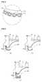
- Fig. 6is a perspective view of a lighting device 1B according to a second embodiment.
- Fig. 7is an exploded perspective view of the lighting device 1B of Fig. 6 .
- Fig. 8is a view showing an enlarged area denoted by "A" of Fig. 7 .
- the lighting device 1Bincludes a heat radiating body 40 including a first receiving groove 47 formed on the bottom surface thereof, a reflective structure 30 being disposed in the first receiving groove 47 and reflecting incident light to the outside, a light emitting module unit 20 formed in the circumference of the bottom surface of the heat radiating body 40, and a reflective cover 10 being formed under the light emitting module unit 20 and including a plurality of lenses 11b reflecting light emitted from the light emitting module unit 20 to the reflective structure 30.
- the lighting device 1B according to the second embodimentis similar to the lighting device 1 according to the first embodiment, except the shape of the reflective cover 10b.
- the reflective cover 10bmay have a circular shape or a polygonal ring shape.
- the inner surface of the reflective cover 10bincludes a plurality of concave surfaces.
- the plurality of the concave surfacesare radially arranged at a regular interval on the inner surface of the reflective cover 10b. At least one the concave surface is required.
- the concave surfacemay have a constant curvature or a polygonal surface. The concave surface performs a function of collecting substantially light emitted from the light emitting module unit in a particular direction.
- the concave surfaceis designated as a lens 11b.
- the plurality of the lenses 11bmay have shapes capable of effectively reflecting light incident from the light emitting module unit 20 to the reflective structure 30, for example, a shape of a hemisphere having a cut part. There is no limit to the shape of the lens 11b.
- the plurality of the lenses 11b of the reflective cover 10bmay be formed to correspond to the plurality of the light emitting devices 22 of the light emitting module unit 20.
- the plurality of the lenses 11bcan be hereby designed such that light emitted from each of the plurality of the light emitting devices 22 proceeds to the reflective structure 30.
- the plurality of the lenses 11bmay have a one-to-one correspondence or one-to-many correspondence with the plurality of the light emitting devices 22. Meanwhile, a correspondence ratio between the plurality of the lenses 11b and the plurality of the light emitting devices 22 may be changed according to a lighting provided by the lighting device 1B. There is no limit to the correspondence ratio.
- the plurality of the light emitting devices 22emit light having many colors
- the plurality of the lenses 11bshould have a one-to-many correspondence with the plurality of the light emitting devices 22.
- light emitting devices emitting red light, green light and blue light respectivelymay correspond to one lens 11b.
- a light emitting device emitting visible light and a following light emitting device emitting ultraviolet light capable of reacting with a photo catalytic materialmay correspond to one lens 11b.
- Fig. 9is a view showing various examples of the shape of the reflective cover 10b including the plurality of the lenses 11b.
- the inner surface and outer surface of the reflective cover 10bmay be curved.
- the inner surface and outer surface of the reflective cover 10bmay have a polygonal surface.
- the inner surface of the reflective cover 10bmay be curved and the outer surface of the reflective cover 10b may be flat.
- the shape of the reflective cover 10b including the plurality of the lenses 11bcan be variously changed according to the design of the lighting device 1B. There is no limit to the shape of the reflective cover 10b.
- a photo catalytic material 12b and a fluorescent materialmay be formed on the inner surfaces of the plurality of the lenses 11b.
- the photo catalytic material 12breacts with light emitted from the light emitting module unit 20 and decomposes impurities, and then hereby prevents the reflective cover 10b from being polluted and maintains the light intensity of the lighting device 1B.
- the fluorescent materialis excited by a first light emitted from the light emitting module unit 20, thus generating a second light. Accordingly, the lighting device 1B can provide light with a wavelength changed by mixing the first light with the second light.
- a separate covermay be further formed under the reflective cover 10b in order to protect the reflective cover 10b which includes the plurality of the lenses 11b.
- a separate coverthere is no limit to the separate cover.
- Fig. 10is a cross sectional view of a lighting device 1C according to a third embodiment.
- the lighting device 1Cincludes a heat radiating body 40 including a first receiving groove 47 formed on the bottom surface thereof, a reflective structure 30 being disposed in the first receiving groove 47 and reflecting incident light to the outside and including a phosphor luminescent film (PLF) 35 in the inner surface thereof, a light emitting module unit 20 formed in the circumference of the bottom surface of the heat radiating body 40, and a reflective cover 10 being formed under the light emitting module unit 20 and reflecting light emitted from the light emitting module unit 20 to the reflective structure 30.
- PPFphosphor luminescent film
- the lighting device 1C according to the third embodimentis the same as the lighting device 1 according to the first embodiment, except the existence of the phosphor luminescent film (PLF) 35 on the inner surface of the reflective structure 30.
- PPFphosphor luminescent film
- the phosphor luminescent film (PLF) 35is a silicon or resin-made thin film including a fluorescent material.
- the fluorescent materialis excited by a first light incident on the reflective structure 30 and generates a second light.
- the reflective structure 30can emit light mixed with the first light and the second light.
- the wavelength of the light incident from the reflective cover 10may be changed by the phosphor luminescent film (PLF) 35 attached to the inner surface of the reflective structure 30.
- the lighting device 1Ccan display various color senses.
- the reflective structure 30may have a phosphor luminescent function of its own instead of disposing a separate phosphor luminescent film (PLF) on the inner surface of the reflective structure 30. That is, in the embodiment, it is possible to substitute the reflective structure 30 with a phosphor luminescent plate having a shape of a flat plate made of a hard material, instead of the phosphor luminescent film (PLF) 35. Accordingly, light emitted from the light emitting module unit 20 is reflected by the reflective cover 10 and is incident on the reflective structure 30, and then the incident light is reflected again and is emitted to the outside. Here, the light incident from the reflective cover 10 has a changed wavelength and is emitted to the outside.
- Fig. 11is a cross sectional view of a lighting device 1D according to a fourth embodiment.
- the lighting device 1Dincludes a heat radiating body 40 including a first receiving groove 47 formed on the bottom surface thereof, a reflective structure 30 disposed in the first receiving groove 47, a reflective cover 10 being formed in the circumference of the bottom surface of the heat radiating body 40 and including an inner groove 17 thereinside, and a light emitting module unit 20 being disposed inside the inner groove 17 of the reflective cover 10 and emitting light to the side wall of the inner groove 17.
- the lighting device 1D according to the fourth embodimentis the same as the lighting device 1 according to the first embodiment, except the shape of the reflective cover 10 and a position in which the light emitting module unit 20 is formed.
- the reflective cover 10includes the inner groove 17 thereinside.
- the light emitting module unit 20is formed in the lower part of the inner groove 17. Here, the light emitting module unit 20 emits light to the side wall of the inner groove 17. Then, the light reflected by the side wall can be incident on the reflective structure 30.
- the light emitting module unit 20 of the lighting device 1Dcan have the same effect as that of the first embodiment by emitting light in the side direction instead of emitting the light downward as described in the first embodiment.
Landscapes
- Engineering & Computer Science (AREA)
- General Engineering & Computer Science (AREA)
- Physics & Mathematics (AREA)
- Microelectronics & Electronic Packaging (AREA)
- Optics & Photonics (AREA)
- Arrangement Of Elements, Cooling, Sealing, Or The Like Of Lighting Devices (AREA)
- Non-Portable Lighting Devices Or Systems Thereof (AREA)
Description
- This embodiment relates to a lighting device.
- A light emitting diode (hereinafter, referred to as LED) is a semiconductor element for converting electric energy into light. As compared with existing light sources such as a fluorescent lamp and an incandescent electric lamp and so on, the LED has advantages of low power consumption, a semi-permanent span of life, a rapid response speed, safety and an environment-friendliness. For this reason, many researches are devoted to substitution of the existing light sources with the LED. The LED is now increasingly used as a light source for lighting devices, for example, various lamps used interiorly and exteriorly, a liquid crystal display device, an electric sign and a street lamp and the like, as shown in
KR 2009 0046120 - One embodiment is a lighting device. The lighting device includes:
- a heat radiating body including a receiving groove;
- a reflective structure being disposed in the first receiving groove and reflecting incident light to the outside;
- a light emitting module unit being disposed on the circumference of the lower part of the heat radiating body and emitting light; and
- a cover being disposed under the light emitting module unit and reflecting light emitted from the light emitting module unit to the reflective structure.
Fig. 1 is a perspective view of a lighting device according to a first embodiment.Fig. 2 is an exploded perspective view of the lighting device ofFig. 1 .Fig. 3 is a cross sectional view of the lighting device ofFig. 1 .Fig. 4 is a cross sectional view showing another embodiment of a heat radiating body of the lighting device ofFig. 1 .Fig. 5 is a plan view showing another embodiment of a light emitting module unit of the lighting device ofFig. 1 .Fig. 6 is a perspective view of a lighting device according to a second embodiment.Fig. 7 is an exploded perspective view of the lighting device ofFig. 6 .Fig. 8 is a view showing an enlarged area denoted by "A" ofFig. 7 .Fig. 9 is a view showing various examples of a reflective cover of the lighting device ofFig. 6 .Fig. 10 is a cross sectional view of a lighting device according to a third embodiment.Fig. 11 is a cross sectional view of a lighting device according to a fourth embodiment.- Hereinafter, an embodiment of the present invention will be described in detail with reference to the accompanying drawings.
- It will be understood that when an element is referred to as being 'on' or "under" another element, it can be directly on/under the element, and one or more intervening elements may also be present.
Fig. 1 is a perspective view of alighting device 1 according to a first embodiment.Fig. 2 is an exploded perspective view of thelighting device 1.Fig. 3 is a cross sectional view of thelighting device 1.- Referring to
Figs. 1 to 3 , thelighting device 1 according to the first embodiment includes aheat radiating body 40 including a first receivinggroove 47 formed on the bottom surface thereof, areflective structure 30 disposed in thefirst receiving groove 47, a lightemitting module unit 20 formed in the circumference of the bottom surface of theheat radiating body 40, and areflective cover 10 being formed under the lightemitting module unit 20 and reflecting light emitted from the lightemitting module unit 20 to thereflective structure 30. - A second receiving
groove 48 may be formed on the top surface of theheat radiating body 40. Apower supply controller 50 may be disposed in thesecond receiving groove 48. Thepower supply controller 50 is electrically connected to the lightemitting module unit 20, thus providing electric power and/or a driving signal to the lightemitting module unit 20. - The
lighting device 1 according to the first embodiment is attached or coupled to an external support member (not shown) such as a ceiling or a surface of a wall and the like, thus providing light. Here, the light emitted from the lightemitting module unit 20 is reflected by thereflective cover 10 and is incident toward thereflective structure 30. The light incident toward thereflective structure 30 is reflected again by thereflective structure 30 and is provided to the outside. That is, thelighting device 1 according to the first embodiment can provide subdued light with reduced glare through the at least two reflections. - The
lighting device 1 according to the first embodiment can provide light through the two reflections such that various operations, for example, wavelength variation of the light and photo catalyst reaction, etc., are generated. Detailed description thereabout will be made in detail later. - Hereinafter, the components and operations of the
lighting device 1 according to the first embodiment will be described in detail. - The
heat radiating body 40 constitutes a body of thelighting device 1 as well as radiates heat generated from the lightemitting module unit 20. - The
heat radiating body 40 is made of a metallic material or a resin material which has high heat radiation efficiency. However, the material of theheat radiating body 40 is not limited to this. For example, the material of theheat radiating body 40 may include at least one of Al, Ni, Cu, Ag and Sn. - A prominence and
depression structure 41 may be formed on the side of theheat radiating body 40 in order to maximize the heat radiation efficiency by enlarging the surface area of theheat radiating body 40. The shape of the prominence anddepression structure 41 can be variously changed according to the design of thelighting device 1. - The first receiving
groove 47 is formed on the bottom surface of theheat radiating body 40. The second receivinggroove 48 is formed on the top surface of theheat radiating body 40. Thereflective structure 30 may be inserted and disposed in thefirst receiving groove 47. Thepower supply controller 50 may be disposed in thesecond receiving groove 48. However, the second receivinggroove 48 is not necessarily formed. - The shape of the
heat radiating body 40 as viewed from the top is not limited to a circle. Theheat radiating body 40 may have a polygonal shape, an elliptical shape and the like. - The upper area of the
heat radiating body 40 may include afastening member 44 which can be coupled to an external support member (not shown) such as a ceiling or a surface of a wall and the like. For example, theheat radiating body 40 can be coupled to the external support member (not shown) by inserting a coupling screw into the hole formed in thefastening member 44. - As shown in
Fig. 4 , ascrew groove 44b is formed in the upper part of theheat radiating body 40, so that thelighting device 1 may be rotated and fixed to a coupling groove formed in the external support member (not shown). However, there is no limit to the method for attaching or coupling thelighting device 1 to the external support member (not shown). - A
level difference portion 42 may be formed in the lower part of theheat radiating body 40 so as to couple thereflective cover 10 to theheat radiating body 40. Thereflective cover 10 may be coupled to thelevel difference portion 42 by means of acoupling screw 14 and the like. However, the method for coupling thereflective cover 10 to theheat radiating body 40 is not limited to this. - The light
emitting module unit 20 is formed in the circumference of the bottom surface of theheat radiating body 40. That is, the lightemitting module unit 20 is formed outside the first receivinggroove 47 of the bottom surface of theheat radiating body 40. - The light emitting
module unit 20 may include asubstrate 21 and a plurality of light emittingdevices 22 mounted on thesubstrate 21. - The
substrate 21 is made by printing a circuit pattern on an insulator. Thesubstrate 21 may include one of a printed circuit board (PCB), a flexible PCB, a metal core PCB, a ceramic PCB and a PCB made of other materials. - The
substrate 21 has a shape corresponding to the shape of theheat radiating body 40. As shown inFigs. 1 and2 , if the shape of theheat radiating body 40 as viewed from the top is a circle, the shape of thesubstrate 21 may be a circular ring. - Meanwhile, when it is difficult to manufacture the circular ring-shaped
substrate 21a, a plurality of straight line shapedsubstrates 21a are provided and, as shown inFig. 5 , coupled to each other in the form of a polygonal ring close to a circular shape. The shape of thesubstrate 21 is not limited to this. - Each of the plurality of the
light emitting devices 22 may include at least one light emitting diode (hereinafter, referred to as LED). The LED may emit ultraviolet (UV) light, infrared (IR) light and visible light including red light, green light, blue light and white light, etc. However, there is no limit to the number and kind of the light emitted by the LED. - Meanwhile, a
heat radiating plate 27 is disposed between the light emittingmodule unit 20 and theheat radiating body 40. For example, after theheat radiating plate 27 is attached to the circumference of the bottom surface of theheat radiating body 40, the light emittingmodule unit 20 is attached to theheat radiating plate 27. Theheat radiating plate 27 is formed of a thermal conductive tape or a thermal conductive adhesive, etc. The material of theheat radiating plate 27 is not limited to this. - The
reflective structure 30 is partially inserted and disposed in the first receivinggroove 47 formed on the bottom surface of theheat radiating body 40. Thereflective structure 30 reflects the light incident from thereflective cover 10 and provides the light to the outside. - As shown in
Fig. 3 , thereflective structure 30 includes a hemispherical shapereflective surface 32 and anedge 31 around thereflective surface 32. - For example, the
edge 31 is disposed under thesubstrate 21 of the light emittingmodule unit 20 and is coupled to thesubstrate 21 by using an adhesive or a coupling screw. Thereflective surface 32 is partially inserted and disposed in the first receivinggroove 47. - Meanwhile, the shape of the
reflective surface 32 of thereflective structure 30 is not limited to a hemispherical shape. For example, thereflective surface 32 may have a shape of a hemisphere with a depressed vertex, that is, a parabola having a section with two parabolic surfaces. The shape of thereflective surface 32 can be changed according to a design of thelighting device 1. - The material of the
reflective structure 30 may include a metallic material or a resin material which has high reflection efficiency or may be formed of the metallic material or the resin material. The metallic material includes, for example, at least one of Ag, an alloy including Ag, Al, an alloy including Al. The resin material includes PET resin, PC resin, PVC resin and the like. - The surface of the
reflective structure 30 may be coated with white photo solder resist (PSR), Ag, Al and the like, which have high reflection efficiency. - Otherwise, the first receiving
groove 47 is formed to have a reflective surface having a hemispherical shape and the like with high reflection efficiency without formation of thereflective structure 30. The kind of thereflective structure 30 is not limited to this. - The
reflective cover 10 is formed under the light emittingmodule unit 20 and reflects light emitted from the light emittingmodule unit 20 to thereflective structure 30. Thereflective cover 10 may include anopening 15 for allowing the light reflected from thereflective structure 30 to be emitted to the outside. - The inner surface of the
reflective cover 10 may be curved such that the light is reflected and emitted to thereflective structure 30 by adjusting the orientation angle of the light emitted from the light emittingmodule unit 20. The curvature of the curved surface of the inner surface can be variously determined according to the design of thelighting device 1. Meanwhile, the inner surface of thereflective cover 10 may have a polygonal surface. The shape of the inner surface is not limited to this. - As shown in
Fig. 3 , thereflective cover 10 can be, for example, coupled by means of thecoupling screw 14 and the like to thelevel difference portion 42 formed in the lower part of theheat radiating body 40. However, there is no limit to the method for coupling thereflective cover 10 to theheat radiating body 40. - The
reflective cover 10 may include a metallic material or a resin material which has high reflection efficiency or may be formed of the metallic material or the resin material. The metallic material includes, for example, at least one of Ag, an alloy including Ag, Al, an alloy including Al. The resin material includes PET resin, PC resin, PVC resin and the like. - The surface of the
reflective cover 10 may be coated with white photo solder resist (PSR), Ag, Al and the like, which have high reflection efficiency. - As such, since the light emitted from the light emitting
module unit 20 is reflected by thereflective cover 10 and thereflective structure 30 and is emitted to the outside, thelighting device 1 can provide subdued light with reduced glare. - Meanwhile, at least one of a photo
catalytic material 12 or a fluorescent material may be formed on the inner surface of thereflective cover 10. As a result, light emitted from the light emittingmodule unit 20 is provided performing various functions, such as pollution prevention by the photocatalytic material 12 or/and the fluorescent material formed on the inner surface of thereflective cover 10. Hereinafter, the description thereabout will be made in detailed later. - The photo
catalytic material 12 may include, for example, titanium oxide (TiO2). The titanium oxide (TiO2) oxides, decomposes and removes impurities by causing a chemical reaction by means of light with an ultra violet wavelength or a blue wavelength of about 200 nm to 450 nm. - In other words, the photo
catalytic material 12 is formed on the inner surface of thereflective cover 10 and prevents thereflective cover 10 from being polluted by impurities, so that the light intensity of thelighting device 1 can be maintained. - The plurality of the
light emitting devices 22 of the light emittingmodule unit 20 emit light with an ultra violet wavelength by which the titanium oxide (TiO2) causes a chemical reaction, or emit light with a blue wavelength of about 200 nm to 450 nm. Here, when the titanium oxide (TiO2) is used as the photocatalytic material 12, it is desirable that at least one portion of the plurality of thelight emitting devices 22 is used. - The photo
catalytic material 12 may be coated or spray-coated on the inner surface of thereflective cover 10 in the form of a thin film. However, there is no limit to the method for forming the photocatalytic material 12. - The fluorescent material is excited by a first light emitted from the light emitting
module unit 20, thus generating a second light. Accordingly, light mixed with the first light and the second light is generated by the fluorescent material. As a result, the wavelength of the light provided by thelighting device 1 can be changed. - The fluorescent material is included in a resin material or a silicon material and is formed on the inner surface of the
reflective cover 10 by using a coating method and the like. On the other hand, a phosphor luminescent film (PLF) including the fluorescent material is provided, and then the phosphor luminescent film (PLF) may be attached to the inner surface of thereflective cover 10. There is no limit to a method for forming the fluorescent material. - The
power supply controller 50 is disposed in the second receivinggroove 48 of the top surface of theheat radiating body 40. - The
power supply controller 50 receives electric power from an external power supply and converts the electric power into electric power of a type suitable for the light emittingmodule unit 20 and then transmits. For example, thepower supply controller 50 may be formed to include at least one selected from a group consisting of a direct current-direct current converter converting alternating current into direct current, a protective device for protecting an electro static discharge (ESD) of the light emittingmodule unit 20, a driving chip for controlling and driving the light emittingmodule unit 20, and a micro processor and the like. - While not shown, the
power supply controller 50 can be electrically connected to the light emittingmodule unit 20 through a wiring. For example, a through hole is formed to pass through the top surface and the bottom surface of theheat radiating body 40, and then the wiring is capable of connecting the light emittingmodule unit 20 to thepower supply controller 50 through the through hole. - Hereinafter, a lighting device 1B according to a second embodiment will be described in detail. However, in description of the second embodiment, repetitive descriptions of the first embodiment will be omitted or briefly described.
Fig. 6 is a perspective view of a lighting device 1B according to a second embodiment.Fig. 7 is an exploded perspective view of the lighting device 1B ofFig. 6 .Fig. 8 is a view showing an enlarged area denoted by "A" ofFig. 7 .- Referring to
Figs. 6 to 8 , the lighting device 1B includes aheat radiating body 40 including a first receivinggroove 47 formed on the bottom surface thereof, areflective structure 30 being disposed in the first receivinggroove 47 and reflecting incident light to the outside, a light emittingmodule unit 20 formed in the circumference of the bottom surface of theheat radiating body 40, and areflective cover 10 being formed under the light emittingmodule unit 20 and including a plurality oflenses 11b reflecting light emitted from the light emittingmodule unit 20 to thereflective structure 30. - The lighting device 1B according to the second embodiment is similar to the
lighting device 1 according to the first embodiment, except the shape of thereflective cover 10b. - The
reflective cover 10b may have a circular shape or a polygonal ring shape. The inner surface of thereflective cover 10b includes a plurality of concave surfaces. The plurality of the concave surfaces are radially arranged at a regular interval on the inner surface of thereflective cover 10b. At least one the concave surface is required. The concave surface may have a constant curvature or a polygonal surface. The concave surface performs a function of collecting substantially light emitted from the light emitting module unit in a particular direction. - Therefore, in the embodiment, the concave surface is designated as a
lens 11b. - The plurality of the
lenses 11b may have shapes capable of effectively reflecting light incident from the light emittingmodule unit 20 to thereflective structure 30, for example, a shape of a hemisphere having a cut part. There is no limit to the shape of thelens 11b. - The plurality of the
lenses 11b of thereflective cover 10b may be formed to correspond to the plurality of thelight emitting devices 22 of the light emittingmodule unit 20. The plurality of thelenses 11b can be hereby designed such that light emitted from each of the plurality of thelight emitting devices 22 proceeds to thereflective structure 30. - Here, the plurality of the
lenses 11b may have a one-to-one correspondence or one-to-many correspondence with the plurality of thelight emitting devices 22. Meanwhile, a correspondence ratio between the plurality of thelenses 11b and the plurality of thelight emitting devices 22 may be changed according to a lighting provided by the lighting device 1B. There is no limit to the correspondence ratio. - Particularly, when the plurality of the
light emitting devices 22 emit light having many colors, it is required that the plurality of thelenses 11b should have a one-to-many correspondence with the plurality of thelight emitting devices 22. - For example, light emitting devices emitting red light, green light and blue light respectively may correspond to one
lens 11b. Otherwise, a light emitting device emitting visible light and a following light emitting device emitting ultraviolet light capable of reacting with a photo catalytic material may correspond to onelens 11b. There is no limit to the method of correspondence between the light emitting devices and thelens 11b. Fig. 9 is a view showing various examples of the shape of thereflective cover 10b including the plurality of thelenses 11b.- Referring to (a) of
Fig. 9 , the inner surface and outer surface of thereflective cover 10b may be curved. Referring to (b) ofFig. 9 , the inner surface and outer surface of thereflective cover 10b may have a polygonal surface. Referring to (c) ofFig. 9 , the inner surface of thereflective cover 10b may be curved and the outer surface of thereflective cover 10b may be flat. - That is, the shape of the
reflective cover 10b including the plurality of thelenses 11b can be variously changed according to the design of the lighting device 1B. There is no limit to the shape of thereflective cover 10b. - Referring to
Figs. 6 to 8 again, at least one of a photocatalytic material 12b and a fluorescent material may be formed on the inner surfaces of the plurality of thelenses 11b. The photocatalytic material 12b reacts with light emitted from the light emittingmodule unit 20 and decomposes impurities, and then hereby prevents thereflective cover 10b from being polluted and maintains the light intensity of the lighting device 1B. The fluorescent material is excited by a first light emitted from the light emittingmodule unit 20, thus generating a second light. Accordingly, the lighting device 1B can provide light with a wavelength changed by mixing the first light with the second light. - While not shown, a separate cover may be further formed under the
reflective cover 10b in order to protect thereflective cover 10b which includes the plurality of thelenses 11b. Here, there is no limit to the separate cover. - Hereinafter, a
lighting device 1C according to a third embodiment will be described in detail. However, in description of the third embodiment, repetitive descriptions of the first embodiment will be omitted or briefly described. Fig. 10 is a cross sectional view of alighting device 1C according to a third embodiment.- Referring to
Fig. 10 , thelighting device 1C includes aheat radiating body 40 including a first receivinggroove 47 formed on the bottom surface thereof, areflective structure 30 being disposed in the first receivinggroove 47 and reflecting incident light to the outside and including a phosphor luminescent film (PLF) 35 in the inner surface thereof, a light emittingmodule unit 20 formed in the circumference of the bottom surface of theheat radiating body 40, and areflective cover 10 being formed under the light emittingmodule unit 20 and reflecting light emitted from the light emittingmodule unit 20 to thereflective structure 30. - The
lighting device 1C according to the third embodiment is the same as thelighting device 1 according to the first embodiment, except the existence of the phosphor luminescent film (PLF) 35 on the inner surface of thereflective structure 30. - The phosphor luminescent film (PLF) 35 is a silicon or resin-made thin film including a fluorescent material. The fluorescent material is excited by a first light incident on the
reflective structure 30 and generates a second light. Thereflective structure 30 can emit light mixed with the first light and the second light. - That is, the wavelength of the light incident from the
reflective cover 10 may be changed by the phosphor luminescent film (PLF) 35 attached to the inner surface of thereflective structure 30. As a result, thelighting device 1C can display various color senses. - Meanwhile, in the third embodiment, while the
reflective structure 30 and the phosphor luminescent film (PLF) 35 are separately arranged, thereflective structure 30 may have a phosphor luminescent function of its own instead of disposing a separate phosphor luminescent film (PLF) on the inner surface of thereflective structure 30. That is, in the embodiment, it is possible to substitute thereflective structure 30 with a phosphor luminescent plate having a shape of a flat plate made of a hard material, instead of the phosphor luminescent film (PLF) 35. Accordingly, light emitted from the light emittingmodule unit 20 is reflected by thereflective cover 10 and is incident on thereflective structure 30, and then the incident light is reflected again and is emitted to the outside. Here, the light incident from thereflective cover 10 has a changed wavelength and is emitted to the outside. - Hereinafter, a lighting device 1D according to a fourth embodiment will be described in detail. However, in description of the fourth embodiment, repetitive descriptions of the first embodiment will be omitted or briefly described.
Fig. 11 is a cross sectional view of a lighting device 1D according to a fourth embodiment.- Referring to
Fig. 11 , the lighting device 1D includes aheat radiating body 40 including a first receivinggroove 47 formed on the bottom surface thereof, areflective structure 30 disposed in the first receivinggroove 47, areflective cover 10 being formed in the circumference of the bottom surface of theheat radiating body 40 and including an inner groove 17 thereinside, and a light emittingmodule unit 20 being disposed inside the inner groove 17 of thereflective cover 10 and emitting light to the side wall of the inner groove 17. - The lighting device 1D according to the fourth embodiment is the same as the
lighting device 1 according to the first embodiment, except the shape of thereflective cover 10 and a position in which the light emittingmodule unit 20 is formed. - The
reflective cover 10 includes the inner groove 17 thereinside. The light emittingmodule unit 20 is formed in the lower part of the inner groove 17. Here, the light emittingmodule unit 20 emits light to the side wall of the inner groove 17. Then, the light reflected by the side wall can be incident on thereflective structure 30. - That is, the light emitting
module unit 20 of the lighting device 1D can have the same effect as that of the first embodiment by emitting light in the side direction instead of emitting the light downward as described in the first embodiment. - The features, structures and effects and the like described in the embodiments are included in at least one embodiment of the present invention and are not necessarily limited to one embodiment. Furthermore, the features, structures, effects and the like provided in each embodiment can be combined or modified in other embodiments by those skilled in the art to which the embodiments belong. Therefore, contents related to the combination and modification should be construed to be included in the scope of the present invention.
Claims (15)
- A lighting device comprising:a heat radiating body (40) comprising a first receiving groove (47) formed on a bottom surface thereof and a second receiving groove (48) formed on a top surface thereof;a reflective structure (30) being disposed in the first receiving groove (47) and comprising a reflective surface (32) reflecting incident light to the outside, wherein the reflective surface (32) has a hemispherical shape;a light emitting module unit (20) being disposed on the circumference of the bottom surface of the heat radiating body (40) and emitting light;a cover (10) comprising an inner surface being disposed under the light emitting module unit (20) and reflecting light emitted from the light emitting module unit (20) to the reflective structure (30), wherein the cover has an opening (15) for allowing the light reflected from the reflective structure (30) to be emitted to the outside; anda power supply controller (50) disposed in the second receiving groove (48) and electrically connected to the light emitting module unit (20).
- The lighting device of claim 1, wherein the light emitting module unit (20) comprises a plurality of light emitting devices (22), and wherein the inner surface of the cover (10) is curved.
- The lighting device of claim 2, wherein the cover comprises an outer surface, and wherein the outer surface is curved or flat.
- The lighting device of claim 1, wherein the light emitting module unit (20) comprises a plurality of light emitting devices (22), wherein the inner surface of the cover (10) is a ploygonal surface, wherein the cover comprises an outer surface, and wherein the outer surface is a ploygonal surface.
- The lighting device of claim 1, wherein the light emitting module unit (20) comprises a plurality of light emitting devices (22), wherein the inner surface of the cover (10) includes a plurality of concave surfaces (11b) collecting substantially light emitted from the light emitting module unit (20) in a particular direction, and wherein the plurality of the concave surfaces (11b) has a one-to-one correspondence or one-to-many correspondence with the plurality of the light emitting devices (22).
- The lighting device of claim 5, wherein the plurality of the concave surfaces are radially arranged at a regular interval on the inner surface of the cover (10b).
- The lighting device of claim 5 or 6, wherein the each of concave surfaces (11b) has a constant curvature or a polygonal surface.
- The lighting device of any one claim of claims 5 to 7, wherein the plurality of the light emitting devices (22) emit light having different colors each other, and wherein the plurality of the concave surfaces (11b) has a one-to-many correspondence with the plurality of the light emitting devices (22).
- The lighting device of claim any one claim of claims 1 to 8, further comrpising a photo catalytic material (12b) disposed on the inner surface of the cover (10).
- The lighting device of claim any one claim of claims 1 to 8, further comrpising a fluorescent material disposed on the inner surface of the cover (10).
- The lighting device of claim any one claim of claims 1 to 10, further comrpising a phosphor luminescent film (35) disposed on the reflective surface (32).
- The lighting device of claim any one claim of claims 1 to 11, wherein the heat radiating body (40) comprises a level difference portion (42) formed in a lower part thereof and coupled to the cover (10).
- The lighting device of claim any one claim of claims 1 to 12, wherein the heat radiating body (40) comprises a screw groove (44b) formed in an upper part thereof.
- The lighting device of claim any one claim of claims 1 to 13, further comprising a heat radiating plate (27) disposed between the light emitting module unit (20) and the bottom surface of the heat radiating body (40).
- The lighting device of claim any one claim of claims 1 to 14, wherein the light emitting module unit (20) comprises a plurality of straight line shaped substrates (21a) disposed on the bottom surface of the heat radiating body (40), and wherein the plurality of the straight line shaped substrates (21a) are coupled to each other in the form of a polygonal ring close to a circular shape.
Applications Claiming Priority (4)
| Application Number | Priority Date | Filing Date | Title |
|---|---|---|---|
| KR1020090107487AKR101144453B1 (en) | 2009-11-09 | 2009-11-09 | Lighting device |
| KR1020090107489AKR101072220B1 (en) | 2009-11-09 | 2009-11-09 | Lighting device |
| KR1020090107492AKR101114095B1 (en) | 2009-11-09 | 2009-11-09 | Lighting device |
| EP10188261.1AEP2320128B1 (en) | 2009-11-09 | 2010-10-20 | Lighting device |
Related Parent Applications (2)
| Application Number | Title | Priority Date | Filing Date |
|---|---|---|---|
| EP10188261.1ADivisionEP2320128B1 (en) | 2009-11-09 | 2010-10-20 | Lighting device |
| EP10188261.1ADivision-IntoEP2320128B1 (en) | 2009-11-09 | 2010-10-20 | Lighting device |
Publications (3)
| Publication Number | Publication Date |
|---|---|
| EP2863117A2 EP2863117A2 (en) | 2015-04-22 |
| EP2863117A3 EP2863117A3 (en) | 2015-06-10 |
| EP2863117B1true EP2863117B1 (en) | 2016-07-13 |
Family
ID=43558081
Family Applications (2)
| Application Number | Title | Priority Date | Filing Date |
|---|---|---|---|
| EP15151194.6ANot-in-forceEP2863117B1 (en) | 2009-11-09 | 2010-10-20 | Lighting device |
| EP10188261.1ANot-in-forceEP2320128B1 (en) | 2009-11-09 | 2010-10-20 | Lighting device |
Family Applications After (1)
| Application Number | Title | Priority Date | Filing Date |
|---|---|---|---|
| EP10188261.1ANot-in-forceEP2320128B1 (en) | 2009-11-09 | 2010-10-20 | Lighting device |
Country Status (3)
| Country | Link |
|---|---|
| US (2) | US8573802B2 (en) |
| EP (2) | EP2863117B1 (en) |
| CN (1) | CN102072425B (en) |
Families Citing this family (34)
| Publication number | Priority date | Publication date | Assignee | Title |
|---|---|---|---|---|
| US20110110095A1 (en)* | 2009-10-09 | 2011-05-12 | Intematix Corporation | Solid-state lamps with passive cooling |
| US8613528B2 (en)* | 2010-05-07 | 2013-12-24 | Abl Ip Holding Llc | Light fixtures comprising an enclosure and a heat sink |
| CN102777777B (en)* | 2011-05-12 | 2016-03-30 | 欧司朗股份有限公司 | Lighting device and there is the illuminator of this lighting device |
| US8568000B2 (en)* | 2011-08-29 | 2013-10-29 | Tai-Her Yang | Annular-arranged lamp capable of backward projecting by concave sphere |
| KR101326518B1 (en) | 2011-09-02 | 2013-11-07 | 엘지이노텍 주식회사 | Lighting device |
| TWM422646U (en)* | 2011-09-07 | 2012-02-11 | Shi-Ming Chen | Structure of lamp base |
| US20130088848A1 (en) | 2011-10-06 | 2013-04-11 | Intematix Corporation | Solid-state lamps with improved radial emission and thermal performance |
| WO2013052749A2 (en)* | 2011-10-06 | 2013-04-11 | Intematix Corporation | Solid-state lamps with improved radial emission and thermal performance |
| US8992051B2 (en) | 2011-10-06 | 2015-03-31 | Intematix Corporation | Solid-state lamps with improved radial emission and thermal performance |
| KR102017538B1 (en) | 2012-01-31 | 2019-10-21 | 엘지이노텍 주식회사 | Lighting device |
| DE102012003071B4 (en)* | 2012-02-10 | 2014-11-20 | Alfred-Wegener-Institut Helmholtz-Zentrum für Polar- und Meeresforschung | reflector spotlight |
| DE102012206397B4 (en)* | 2012-04-18 | 2021-04-15 | Osram Gmbh | Lighting device with a screen, one side of which is irradiated by a first light source via a reflector and the other side, which is coated with a luminescent material, is irradiated by a second light source |
| US8680755B2 (en) | 2012-05-07 | 2014-03-25 | Lg Innotek Co., Ltd. | Lighting device having reflectors for indirect light emission |
| US9495660B2 (en) | 2013-07-31 | 2016-11-15 | Google Inc. | Inferring social groups through patterns of communication |
| USD748840S1 (en)* | 2014-05-27 | 2016-02-02 | Lumens Co., Ltd | Ceiling light fixture |
| USD767815S1 (en)* | 2014-05-27 | 2016-09-27 | Lumens Co., Ltd. | Ceiling light fixture |
| DE202014103605U1 (en)* | 2014-08-04 | 2014-08-21 | Brillant Ag | Electric light |
| USD769516S1 (en)* | 2014-08-04 | 2016-10-18 | Spring City Electrical Mfg. Co. | Center mount lamp support |
| US9285100B2 (en)* | 2014-08-11 | 2016-03-15 | Min Hsiang Corporation | Lens structure for a vehicular lamp |
| TWI595189B (en)* | 2014-09-02 | 2017-08-11 | Huan-Chiu Chou | Internal reflection lamp |
| US9702539B2 (en) | 2014-10-21 | 2017-07-11 | Cooper Technologies Company | Flow-through luminaire |
| KR101601531B1 (en)* | 2014-11-07 | 2016-03-10 | 주식회사 지엘비젼 | Lighting Device |
| US20170108177A1 (en)* | 2015-10-15 | 2017-04-20 | GE Lighting Solutions, LLC | Indirect color-mixing led module for point-source source application |
| US10100984B2 (en)* | 2015-10-15 | 2018-10-16 | GE Lighting Solutions, LLC | Indirect light mixing LED module for point-source applications |
| DE102016002849A1 (en)* | 2016-03-10 | 2017-09-14 | Selux Aktiengesellschaft | Also down radiating lamp element for a street lighting or street lamp with an annular, downward radiating light source |
| ITUA20162784A1 (en)* | 2016-04-21 | 2017-10-21 | Efore S P A | LED SPOTLIGHT |
| USD847399S1 (en)* | 2017-05-05 | 2019-04-30 | Hubbell Incorporated | Performance high-bay luminaire |
| USD930219S1 (en)* | 2017-05-16 | 2021-09-07 | Olympia Lighting, Inc. | Light fixture |
| EP3431868A1 (en)* | 2017-07-21 | 2019-01-23 | Philips Lighting Holding B.V. | Catadioptric lighting device |
| US10928020B1 (en)* | 2019-08-22 | 2021-02-23 | Usg Interiors, Llc | Light bar for suspended ceiling |
| LU102029B1 (en)* | 2020-09-02 | 2022-03-02 | Bega Gantenbrink Leuchten Kg | Luminaire for generating direct and indirect lighting |
| EP4215802A4 (en)* | 2020-09-21 | 2024-11-13 | Suzhou Opple Lighting Co., Ltd. | LIGHT SOURCE SYSTEM OF A LUMINAIRE AND LUMINAIRE |
| US12007102B2 (en)* | 2022-03-16 | 2024-06-11 | Globe Electric Company Inc. | Trimless recessed light fixture |
| US11879629B2 (en)* | 2022-03-31 | 2024-01-23 | RAB Lighting Inc. | LED light fixture with a heat sink having concentrically segmented fins |
Family Cites Families (45)
| Publication number | Priority date | Publication date | Assignee | Title |
|---|---|---|---|---|
| GB1138878A (en)* | 1966-09-09 | 1969-01-01 | British Lighting Ind Ltd | Artificial sun-bathing enclosure |
| US4755916A (en)* | 1981-07-23 | 1988-07-05 | Collins Dynamics | Combined flood and spot light |
| US4591960A (en)* | 1984-10-02 | 1986-05-27 | Mwc Lighting | Lighting optical system |
| DE3929955A1 (en)* | 1989-09-08 | 1991-03-14 | Inotec Gmbh Ges Fuer Innovativ | LIGHT SPOTLIGHTS |
| AU2263992A (en)* | 1991-05-02 | 1992-12-21 | Ruud Lighting, Inc. | Improved bollard luminaire |
| JPH0581913A (en) | 1991-09-24 | 1993-04-02 | Toshiba Lighting & Technol Corp | Lighting device |
| IT1252026B (en)* | 1991-11-29 | 1995-05-27 | LIGHTING APPARATUS IN PARTICULAR FOR ENVIRONMENTS WITHOUT NATURAL LIGHT | |
| US5488550A (en)* | 1992-11-18 | 1996-01-30 | Yang; Jerry S. C. | Multi purpose lamp |
| US5564065A (en)* | 1995-01-19 | 1996-10-08 | Chelsea Group Ltd. | Carbon monoxide air filter |
| DE29620583U1 (en)* | 1996-11-27 | 1997-02-13 | Kundisch Microtech GmbH & Co. KG, 78056 Villingen-Schwenningen | Lighting fixture with continuously adjustable color change of the light and the light cone |
| US6186649B1 (en)* | 1998-04-16 | 2001-02-13 | Honeywell International Inc. | Linear illumination sources and systems |
| US6149283A (en)* | 1998-12-09 | 2000-11-21 | Rensselaer Polytechnic Institute (Rpi) | LED lamp with reflector and multicolor adjuster |
| JP4527230B2 (en)* | 2000-02-28 | 2010-08-18 | 三菱電機照明株式会社 | Surface-emitting LED light source |
| US6425677B1 (en)* | 2001-02-20 | 2002-07-30 | Prokia Technology Co., Ltd. | Illuminating apparatus using multiple light sources |
| US6655813B1 (en)* | 2002-01-07 | 2003-12-02 | Genlyte Thomas Group Llc | Multi-function luminaire |
| WO2004111532A1 (en)* | 2003-06-16 | 2004-12-23 | Advanced Display Inc. | Planar light source device and display device using the same |
| US7246917B2 (en)* | 2003-08-12 | 2007-07-24 | Illumination Management Solutions, Inc. | Apparatus and method for using emitting diodes (LED) in a side-emitting device |
| CN100492685C (en)* | 2003-12-05 | 2009-05-27 | 三菱电机株式会社 | Light emitting device and lighting fixture using the same |
| TWI233475B (en)* | 2004-01-20 | 2005-06-01 | Jau-Tang Lin | Lighting device with increased brightness |
| WO2005078338A1 (en)* | 2004-02-17 | 2005-08-25 | Kelly William M | A utility lamp |
| JP2005243973A (en)* | 2004-02-26 | 2005-09-08 | Kyocera Corp | Light emitting device and lighting device |
| US7144131B2 (en)* | 2004-09-29 | 2006-12-05 | Advanced Optical Technologies, Llc | Optical system using LED coupled with phosphor-doped reflective materials |
| JP2006179658A (en) | 2004-12-22 | 2006-07-06 | Mitsubishi Electric Corp | Light emitting device |
| US7559664B1 (en)* | 2004-12-27 | 2009-07-14 | John V. Walleman | Low profile backlighting using LEDs |
| EP2021688B1 (en)* | 2006-05-05 | 2016-04-27 | Cree, Inc. | Lighting device |
| US7703945B2 (en)* | 2006-06-27 | 2010-04-27 | Cree, Inc. | Efficient emitting LED package and method for efficiently emitting light |
| DE102006037376A1 (en)* | 2006-08-09 | 2008-02-14 | Patent-Treuhand-Gesellschaft für elektrische Glühlampen mbH | lamp |
| US7396146B2 (en)* | 2006-08-09 | 2008-07-08 | Augux Co., Ltd. | Heat dissipating LED signal lamp source structure |
| DE102006044019B4 (en)* | 2006-09-15 | 2011-12-29 | Stiftung Alfred-Wegener-Institut für Polar- und Meeresforschung Stiftung des öffentlichen Rechts | reflector spotlight |
| US8104923B2 (en)* | 2006-10-12 | 2012-01-31 | Panasonic Corporation | Light-emitting apparatus |
| JP2008135219A (en)* | 2006-11-27 | 2008-06-12 | Phoenix Denki Kk | Luminaire |
| DE102007061304B4 (en)* | 2006-12-19 | 2010-09-02 | Koito Manufacturing Co., Ltd. | vehicle light |
| US20080198572A1 (en)* | 2007-02-21 | 2008-08-21 | Medendorp Nicholas W | LED lighting systems including luminescent layers on remote reflectors |
| US8403531B2 (en)* | 2007-05-30 | 2013-03-26 | Cree, Inc. | Lighting device and method of lighting |
| US7686486B2 (en)* | 2007-06-30 | 2010-03-30 | Osram Sylvania Inc. | LED lamp module |
| JP5077543B2 (en)* | 2007-09-07 | 2012-11-21 | スタンレー電気株式会社 | Vehicle lamp unit |
| KR20090046120A (en)* | 2007-11-05 | 2009-05-11 | 현대자동차주식회사 | LED lighting device |
| US7722222B2 (en)* | 2008-03-24 | 2010-05-25 | Fu Zhun Precision Industry (Shen Zhen) Co., Ltd. | LED lamp assembly |
| US8028537B2 (en)* | 2009-05-01 | 2011-10-04 | Abl Ip Holding Llc | Heat sinking and flexible circuit board, for solid state light fixture utilizing an optical cavity |
| CN101603662A (en)* | 2008-06-13 | 2009-12-16 | 富准精密工业(深圳)有限公司 | Led lamp and lampshade thereof |
| US8142057B2 (en)* | 2009-05-19 | 2012-03-27 | Schneider Electric USA, Inc. | Recessed LED downlight |
| KR20090066262A (en) | 2009-06-03 | 2009-06-23 | 최재민 | LED lamp |
| US20110033346A1 (en)* | 2009-08-04 | 2011-02-10 | Bohlen Johns R | Air cleaner with photo-catalytic oxidizer |
| DE102009042338B4 (en)* | 2009-09-21 | 2019-03-21 | Berchtold Holding Gmbh | surgical light |
| KR101824039B1 (en)* | 2011-07-29 | 2018-01-31 | 엘지이노텍 주식회사 | display apparatus |
- 2010
- 2010-10-20EPEP15151194.6Apatent/EP2863117B1/ennot_activeNot-in-force
- 2010-10-20EPEP10188261.1Apatent/EP2320128B1/ennot_activeNot-in-force
- 2010-11-04USUS12/939,559patent/US8573802B2/enactiveActive
- 2010-11-09CNCN201010543783XApatent/CN102072425B/ennot_activeExpired - Fee Related
- 2013
- 2013-10-08USUS14/049,015patent/US9200761B2/ennot_activeExpired - Fee Related
Also Published As
| Publication number | Publication date |
|---|---|
| EP2863117A3 (en) | 2015-06-10 |
| CN102072425A (en) | 2011-05-25 |
| CN102072425B (en) | 2013-07-17 |
| EP2320128B1 (en) | 2015-02-25 |
| US20140036509A1 (en) | 2014-02-06 |
| US8573802B2 (en) | 2013-11-05 |
| US20110110096A1 (en) | 2011-05-12 |
| EP2320128A3 (en) | 2013-01-02 |
| EP2863117A2 (en) | 2015-04-22 |
| US9200761B2 (en) | 2015-12-01 |
| EP2320128A2 (en) | 2011-05-11 |
Similar Documents
| Publication | Publication Date | Title |
|---|---|---|
| EP2863117B1 (en) | Lighting device | |
| US10260724B2 (en) | Lighting device | |
| EP2392853B1 (en) | Lighting device | |
| CN102449386B (en) | Reflector system for lighting device | |
| US9217553B2 (en) | LED lighting systems including luminescent layers on remote reflectors | |
| US8672512B2 (en) | Omni reflective optics for wide angle emission LED light bulb | |
| EP2623845B1 (en) | Lighting device | |
| WO2021018291A1 (en) | Led lamp | |
| JP6956110B2 (en) | Lighting device | |
| EP2753873B1 (en) | Lighting device | |
| KR101072220B1 (en) | Lighting device | |
| KR101114095B1 (en) | Lighting device | |
| US10578273B2 (en) | Lighting apparatus | |
| KR101144453B1 (en) | Lighting device | |
| KR101929256B1 (en) | Lighting device | |
| KR101860039B1 (en) | Lighting device | |
| KR20130005372A (en) | Lighting device |
Legal Events
| Date | Code | Title | Description |
|---|---|---|---|
| PUAI | Public reference made under article 153(3) epc to a published international application that has entered the european phase | Free format text:ORIGINAL CODE: 0009012 | |
| 17P | Request for examination filed | Effective date:20150114 | |
| AC | Divisional application: reference to earlier application | Ref document number:2320128 Country of ref document:EP Kind code of ref document:P | |
| AK | Designated contracting states | Kind code of ref document:A2 Designated state(s):AL AT BE BG CH CY CZ DE DK EE ES FI FR GB GR HR HU IE IS IT LI LT LU LV MC MK MT NL NO PL PT RO RS SE SI SK SM TR | |
| PUAL | Search report despatched | Free format text:ORIGINAL CODE: 0009013 | |
| AK | Designated contracting states | Kind code of ref document:A3 Designated state(s):AL AT BE BG CH CY CZ DE DK EE ES FI FR GB GR HR HU IE IS IT LI LT LU LV MC MK MT NL NO PL PT RO RS SE SI SK SM TR | |
| RIC1 | Information provided on ipc code assigned before grant | Ipc:F21S 8/00 20060101ALI20150504BHEP Ipc:F21V 29/00 20150101AFI20150504BHEP Ipc:F21V 7/00 20060101ALI20150504BHEP | |
| R17P | Request for examination filed (corrected) | Effective date:20150521 | |
| RBV | Designated contracting states (corrected) | Designated state(s):AL AT BE BG CH CY CZ DE DK EE ES FI FR GB GR HR HU IE IS IT LI LT LU LV MC MK MT NL NO PL PT RO RS SE SI SK SM TR | |
| GRAP | Despatch of communication of intention to grant a patent | Free format text:ORIGINAL CODE: EPIDOSNIGR1 | |
| INTG | Intention to grant announced | Effective date:20160126 | |
| GRAS | Grant fee paid | Free format text:ORIGINAL CODE: EPIDOSNIGR3 | |
| GRAA | (expected) grant | Free format text:ORIGINAL CODE: 0009210 | |
| AC | Divisional application: reference to earlier application | Ref document number:2320128 Country of ref document:EP Kind code of ref document:P | |
| AK | Designated contracting states | Kind code of ref document:B1 Designated state(s):AL AT BE BG CH CY CZ DE DK EE ES FI FR GB GR HR HU IE IS IT LI LT LU LV MC MK MT NL NO PL PT RO RS SE SI SK SM TR | |
| REG | Reference to a national code | Ref country code:GB Ref legal event code:FG4D | |
| REG | Reference to a national code | Ref country code:AT Ref legal event code:REF Ref document number:812647 Country of ref document:AT Kind code of ref document:T Effective date:20160715 Ref country code:CH Ref legal event code:EP | |
| REG | Reference to a national code | Ref country code:IE Ref legal event code:FG4D | |
| REG | Reference to a national code | Ref country code:DE Ref legal event code:R096 Ref document number:602010034778 Country of ref document:DE | |
| REG | Reference to a national code | Ref country code:FR Ref legal event code:PLFP Year of fee payment:7 | |
| REG | Reference to a national code | Ref country code:NL Ref legal event code:FP | |
| REG | Reference to a national code | Ref country code:LT Ref legal event code:MG4D | |
| REG | Reference to a national code | Ref country code:AT Ref legal event code:MK05 Ref document number:812647 Country of ref document:AT Kind code of ref document:T Effective date:20160713 | |
| PG25 | Lapsed in a contracting state [announced via postgrant information from national office to epo] | Ref country code:LT Free format text:LAPSE BECAUSE OF FAILURE TO SUBMIT A TRANSLATION OF THE DESCRIPTION OR TO PAY THE FEE WITHIN THE PRESCRIBED TIME-LIMIT Effective date:20160713 Ref country code:HR Free format text:LAPSE BECAUSE OF FAILURE TO SUBMIT A TRANSLATION OF THE DESCRIPTION OR TO PAY THE FEE WITHIN THE PRESCRIBED TIME-LIMIT Effective date:20160713 Ref country code:FI Free format text:LAPSE BECAUSE OF FAILURE TO SUBMIT A TRANSLATION OF THE DESCRIPTION OR TO PAY THE FEE WITHIN THE PRESCRIBED TIME-LIMIT Effective date:20160713 Ref country code:RS Free format text:LAPSE BECAUSE OF FAILURE TO SUBMIT A TRANSLATION OF THE DESCRIPTION OR TO PAY THE FEE WITHIN THE PRESCRIBED TIME-LIMIT Effective date:20160713 Ref country code:IS Free format text:LAPSE BECAUSE OF FAILURE TO SUBMIT A TRANSLATION OF THE DESCRIPTION OR TO PAY THE FEE WITHIN THE PRESCRIBED TIME-LIMIT Effective date:20161113 Ref country code:NO Free format text:LAPSE BECAUSE OF FAILURE TO SUBMIT A TRANSLATION OF THE DESCRIPTION OR TO PAY THE FEE WITHIN THE PRESCRIBED TIME-LIMIT Effective date:20161013 Ref country code:IT Free format text:LAPSE BECAUSE OF FAILURE TO SUBMIT A TRANSLATION OF THE DESCRIPTION OR TO PAY THE FEE WITHIN THE PRESCRIBED TIME-LIMIT Effective date:20160713 | |
| PG25 | Lapsed in a contracting state [announced via postgrant information from national office to epo] | Ref country code:AT Free format text:LAPSE BECAUSE OF FAILURE TO SUBMIT A TRANSLATION OF THE DESCRIPTION OR TO PAY THE FEE WITHIN THE PRESCRIBED TIME-LIMIT Effective date:20160713 Ref country code:PL Free format text:LAPSE BECAUSE OF FAILURE TO SUBMIT A TRANSLATION OF THE DESCRIPTION OR TO PAY THE FEE WITHIN THE PRESCRIBED TIME-LIMIT Effective date:20160713 Ref country code:GR Free format text:LAPSE BECAUSE OF FAILURE TO SUBMIT A TRANSLATION OF THE DESCRIPTION OR TO PAY THE FEE WITHIN THE PRESCRIBED TIME-LIMIT Effective date:20161014 Ref country code:LV Free format text:LAPSE BECAUSE OF FAILURE TO SUBMIT A TRANSLATION OF THE DESCRIPTION OR TO PAY THE FEE WITHIN THE PRESCRIBED TIME-LIMIT Effective date:20160713 Ref country code:PT Free format text:LAPSE BECAUSE OF FAILURE TO SUBMIT A TRANSLATION OF THE DESCRIPTION OR TO PAY THE FEE WITHIN THE PRESCRIBED TIME-LIMIT Effective date:20161114 Ref country code:SE Free format text:LAPSE BECAUSE OF FAILURE TO SUBMIT A TRANSLATION OF THE DESCRIPTION OR TO PAY THE FEE WITHIN THE PRESCRIBED TIME-LIMIT Effective date:20160713 Ref country code:ES Free format text:LAPSE BECAUSE OF FAILURE TO SUBMIT A TRANSLATION OF THE DESCRIPTION OR TO PAY THE FEE WITHIN THE PRESCRIBED TIME-LIMIT Effective date:20160713 Ref country code:BE Free format text:LAPSE BECAUSE OF NON-PAYMENT OF DUE FEES Effective date:20160713 | |
| REG | Reference to a national code | Ref country code:DE Ref legal event code:R097 Ref document number:602010034778 Country of ref document:DE | |
| PG25 | Lapsed in a contracting state [announced via postgrant information from national office to epo] | Ref country code:RO Free format text:LAPSE BECAUSE OF FAILURE TO SUBMIT A TRANSLATION OF THE DESCRIPTION OR TO PAY THE FEE WITHIN THE PRESCRIBED TIME-LIMIT Effective date:20160713 Ref country code:EE Free format text:LAPSE BECAUSE OF FAILURE TO SUBMIT A TRANSLATION OF THE DESCRIPTION OR TO PAY THE FEE WITHIN THE PRESCRIBED TIME-LIMIT Effective date:20160713 | |
| RAP2 | Party data changed (patent owner data changed or rights of a patent transferred) | Owner name:LG INNOTEK CO., LTD. | |
| PLBE | No opposition filed within time limit | Free format text:ORIGINAL CODE: 0009261 | |
| STAA | Information on the status of an ep patent application or granted ep patent | Free format text:STATUS: NO OPPOSITION FILED WITHIN TIME LIMIT | |
| PG25 | Lapsed in a contracting state [announced via postgrant information from national office to epo] | Ref country code:SM Free format text:LAPSE BECAUSE OF FAILURE TO SUBMIT A TRANSLATION OF THE DESCRIPTION OR TO PAY THE FEE WITHIN THE PRESCRIBED TIME-LIMIT Effective date:20160713 Ref country code:DK Free format text:LAPSE BECAUSE OF FAILURE TO SUBMIT A TRANSLATION OF THE DESCRIPTION OR TO PAY THE FEE WITHIN THE PRESCRIBED TIME-LIMIT Effective date:20160713 Ref country code:CZ Free format text:LAPSE BECAUSE OF FAILURE TO SUBMIT A TRANSLATION OF THE DESCRIPTION OR TO PAY THE FEE WITHIN THE PRESCRIBED TIME-LIMIT Effective date:20160713 Ref country code:SK Free format text:LAPSE BECAUSE OF FAILURE TO SUBMIT A TRANSLATION OF THE DESCRIPTION OR TO PAY THE FEE WITHIN THE PRESCRIBED TIME-LIMIT Effective date:20160713 Ref country code:BG Free format text:LAPSE BECAUSE OF FAILURE TO SUBMIT A TRANSLATION OF THE DESCRIPTION OR TO PAY THE FEE WITHIN THE PRESCRIBED TIME-LIMIT Effective date:20161013 | |
| REG | Reference to a national code | Ref country code:CH Ref legal event code:PL | |
| 26N | No opposition filed | Effective date:20170418 | |
| GBPC | Gb: european patent ceased through non-payment of renewal fee | Effective date:20161020 | |
| REG | Reference to a national code | Ref country code:IE Ref legal event code:MM4A | |
| PG25 | Lapsed in a contracting state [announced via postgrant information from national office to epo] | Ref country code:CH Free format text:LAPSE BECAUSE OF NON-PAYMENT OF DUE FEES Effective date:20161031 Ref country code:LI Free format text:LAPSE BECAUSE OF NON-PAYMENT OF DUE FEES Effective date:20161031 Ref country code:GB Free format text:LAPSE BECAUSE OF NON-PAYMENT OF DUE FEES Effective date:20161020 | |
| PG25 | Lapsed in a contracting state [announced via postgrant information from national office to epo] | Ref country code:SI Free format text:LAPSE BECAUSE OF FAILURE TO SUBMIT A TRANSLATION OF THE DESCRIPTION OR TO PAY THE FEE WITHIN THE PRESCRIBED TIME-LIMIT Effective date:20160713 Ref country code:LU Free format text:LAPSE BECAUSE OF NON-PAYMENT OF DUE FEES Effective date:20161020 | |
| REG | Reference to a national code | Ref country code:FR Ref legal event code:PLFP Year of fee payment:8 | |
| PG25 | Lapsed in a contracting state [announced via postgrant information from national office to epo] | Ref country code:IE Free format text:LAPSE BECAUSE OF NON-PAYMENT OF DUE FEES Effective date:20161020 | |
| PG25 | Lapsed in a contracting state [announced via postgrant information from national office to epo] | Ref country code:HU Free format text:LAPSE BECAUSE OF FAILURE TO SUBMIT A TRANSLATION OF THE DESCRIPTION OR TO PAY THE FEE WITHIN THE PRESCRIBED TIME-LIMIT; INVALID AB INITIO Effective date:20101020 | |
| PG25 | Lapsed in a contracting state [announced via postgrant information from national office to epo] | Ref country code:CY Free format text:LAPSE BECAUSE OF FAILURE TO SUBMIT A TRANSLATION OF THE DESCRIPTION OR TO PAY THE FEE WITHIN THE PRESCRIBED TIME-LIMIT Effective date:20160713 Ref country code:MT Free format text:LAPSE BECAUSE OF NON-PAYMENT OF DUE FEES Effective date:20161031 Ref country code:MK Free format text:LAPSE BECAUSE OF FAILURE TO SUBMIT A TRANSLATION OF THE DESCRIPTION OR TO PAY THE FEE WITHIN THE PRESCRIBED TIME-LIMIT Effective date:20160713 Ref country code:MC Free format text:LAPSE BECAUSE OF FAILURE TO SUBMIT A TRANSLATION OF THE DESCRIPTION OR TO PAY THE FEE WITHIN THE PRESCRIBED TIME-LIMIT Effective date:20160713 | |
| REG | Reference to a national code | Ref country code:FR Ref legal event code:PLFP Year of fee payment:9 | |
| PG25 | Lapsed in a contracting state [announced via postgrant information from national office to epo] | Ref country code:TR Free format text:LAPSE BECAUSE OF FAILURE TO SUBMIT A TRANSLATION OF THE DESCRIPTION OR TO PAY THE FEE WITHIN THE PRESCRIBED TIME-LIMIT Effective date:20160713 Ref country code:AL Free format text:LAPSE BECAUSE OF FAILURE TO SUBMIT A TRANSLATION OF THE DESCRIPTION OR TO PAY THE FEE WITHIN THE PRESCRIBED TIME-LIMIT Effective date:20160713 | |
| REG | Reference to a national code | Ref country code:NL Ref legal event code:PD Owner name:SUZHOU LEKIN SEMICONDUCTOR CO., LTD.; CN Free format text:DETAILS ASSIGNMENT: CHANGE OF OWNER(S), ASSIGNMENT; FORMER OWNER NAME: LG INNOTEK CO., LTD. Effective date:20210719 | |
| REG | Reference to a national code | Ref country code:DE Ref legal event code:R081 Ref document number:602010034778 Country of ref document:DE Owner name:SUZHOU LEKIN SEMICONDUCTOR CO. LTD., TAICANG, CN Free format text:FORMER OWNER: LG INNOTEK CO., LTD., SEOUL/SOUL, KR | |
| PGFP | Annual fee paid to national office [announced via postgrant information from national office to epo] | Ref country code:NL Payment date:20220916 Year of fee payment:13 | |
| PGFP | Annual fee paid to national office [announced via postgrant information from national office to epo] | Ref country code:FR Payment date:20220908 Year of fee payment:13 | |
| PGFP | Annual fee paid to national office [announced via postgrant information from national office to epo] | Ref country code:DE Payment date:20220621 Year of fee payment:13 | |
| REG | Reference to a national code | Ref country code:DE Ref legal event code:R119 Ref document number:602010034778 Country of ref document:DE | |
| REG | Reference to a national code | Ref country code:NL Ref legal event code:MM Effective date:20231101 | |
| PG25 | Lapsed in a contracting state [announced via postgrant information from national office to epo] | Ref country code:NL Free format text:LAPSE BECAUSE OF NON-PAYMENT OF DUE FEES Effective date:20231101 | |
| PG25 | Lapsed in a contracting state [announced via postgrant information from national office to epo] | Ref country code:NL Free format text:LAPSE BECAUSE OF NON-PAYMENT OF DUE FEES Effective date:20231101 Ref country code:FR Free format text:LAPSE BECAUSE OF NON-PAYMENT OF DUE FEES Effective date:20231031 Ref country code:DE Free format text:LAPSE BECAUSE OF NON-PAYMENT OF DUE FEES Effective date:20240501 |