EP2860561B1 - Light source device - Google Patents
Light source deviceDownload PDFInfo
- Publication number
- EP2860561B1 EP2860561B1EP14185341.6AEP14185341AEP2860561B1EP 2860561 B1EP2860561 B1EP 2860561B1EP 14185341 AEP14185341 AEP 14185341AEP 2860561 B1EP2860561 B1EP 2860561B1
- Authority
- EP
- European Patent Office
- Prior art keywords
- holder
- light
- light source
- optical fiber
- source device
- Prior art date
- Legal status (The legal status is an assumption and is not a legal conclusion. Google has not performed a legal analysis and makes no representation as to the accuracy of the status listed.)
- Not-in-force
Links
Images


Classifications
- G—PHYSICS
- G02—OPTICS
- G02B—OPTICAL ELEMENTS, SYSTEMS OR APPARATUS
- G02B6/00—Light guides; Structural details of arrangements comprising light guides and other optical elements, e.g. couplings
- G02B6/24—Coupling light guides
- G02B6/42—Coupling light guides with opto-electronic elements
- G02B6/4201—Packages, e.g. shape, construction, internal or external details
- G02B6/4256—Details of housings
- G02B6/4262—Details of housings characterised by the shape of the housing
- G02B6/4263—Details of housings characterised by the shape of the housing of the transisitor outline [TO] can type
- G—PHYSICS
- G02—OPTICS
- G02B—OPTICAL ELEMENTS, SYSTEMS OR APPARATUS
- G02B6/00—Light guides; Structural details of arrangements comprising light guides and other optical elements, e.g. couplings
- G02B6/24—Coupling light guides
- G02B6/42—Coupling light guides with opto-electronic elements
- G02B6/4201—Packages, e.g. shape, construction, internal or external details
- G02B6/4204—Packages, e.g. shape, construction, internal or external details the coupling comprising intermediate optical elements, e.g. lenses, holograms
- G—PHYSICS
- G02—OPTICS
- G02B—OPTICAL ELEMENTS, SYSTEMS OR APPARATUS
- G02B6/00—Light guides; Structural details of arrangements comprising light guides and other optical elements, e.g. couplings
- G02B6/24—Coupling light guides
- G02B6/42—Coupling light guides with opto-electronic elements
- G02B6/4201—Packages, e.g. shape, construction, internal or external details
- G02B6/4219—Mechanical fixtures for holding or positioning the elements relative to each other in the couplings; Alignment methods for the elements, e.g. measuring or observing methods especially used therefor
- G02B6/422—Active alignment, i.e. moving the elements in response to the detected degree of coupling or position of the elements
- G02B6/4225—Active alignment, i.e. moving the elements in response to the detected degree of coupling or position of the elements by a direct measurement of the degree of coupling, e.g. the amount of light power coupled to the fibre or the opto-electronic element
- G—PHYSICS
- G02—OPTICS
- G02B—OPTICAL ELEMENTS, SYSTEMS OR APPARATUS
- G02B6/00—Light guides; Structural details of arrangements comprising light guides and other optical elements, e.g. couplings
- G02B6/24—Coupling light guides
- G02B6/42—Coupling light guides with opto-electronic elements
- G02B6/4201—Packages, e.g. shape, construction, internal or external details
- G02B6/4219—Mechanical fixtures for holding or positioning the elements relative to each other in the couplings; Alignment methods for the elements, e.g. measuring or observing methods especially used therefor
- G02B6/4236—Fixing or mounting methods of the aligned elements
- G02B6/4239—Adhesive bonding; Encapsulation with polymer material
Definitions
- the present inventionrelates to a light source device which converges light flux emitted from a light source on an optical fiber.
- US 2004/0114873 A1discloses: An inexpensive, robust, and adhesive-free method and apparatus is disclosed for efficiently coupling first and second optical components together utilizing a flexure assembly for fine alignment.
- An initial three-dimensional rough alignment processpositions the first and second optical components proximate to each other and aligns them in three dimensions. The first and second components are then misaligned by a fixed amount, causing a defocus, and then securely fastened together.
- the fine alignment processuses standard machine screws, or other easily attainable, robust tensioning means to progressively increase the tension around the periphery of the flexure assembly, which causes the flexure to bend and the second optical component to translate along the longitudinal axis of the flexure assembly and tilt with respect to the longitudinal axis of the flexure assembly, which refocuses and three-dimensionally finely aligns the optical components for optimum coupling efficiency in a simple and secure manner.
- US 2002/0168153 A1discloses: An optical module with a small size and improved mass-productivity.
- the optical modulecomprises a fiber stub including an optical fiber, a sleeve containing the fiber stub, and a semiconductor optical amplifying device.
- a Bragg fiber gratingis formed in the optical fiber.
- the optical fiberis secured in the ferrule.
- the optical amplifying device and the gratingform a laser cavity. Only a part of the hollow portion of the sleeve is filled with a fiber stub.
- One end face of the optical fiberis disposed at one end of the sleeve.
- the other end of the sleeveis hollow.
- the optical moduleacts as an optical receptacle.
- An optical plugcan be inserted into the hollow end of the sleeve. This enables the laser light to be introduced into an external optical device.
- a light source devicewhich converges light flux emitted from a light source on an optical fiber
- a light source devicewhere a light converging lens and a ferrule holder are held by a holder.
- the positional adjustment of the holderis performed in a state where the holder is brought into close contact with a stem to which an optical semiconductor element and a cap are fixed and, thereafter, the holder and the stem are fixed to each other by soldering (see Japanese Patent Application Laid-Open No. 2-32583 , for example).
- the holder and the stemare fixed to each other by soldering or the like using the above-mentioned method and hence, a space for adjustment is required between the holder and a cap. Accordingly, the conventional light source has a drawback that the structure of the holder becomes complicated and the light source device becomes large-sized.
- the light source deviceincludes: an optical semiconductor element which is mounted on a support base; a cap which is fixed to the support base so as to cover the optical semiconductor element; a light converging portion which converges light flux emitted from the optical semiconductor element; an optical fiber connection portion to which an optical fiber is connected, the optical fiber receiving inputting of the light flux converged by the light converging portion; and a holder which holds the optical fiber connection portion, the holder being fixed to the cap.
- the optical fiber connection portionincludes a position adjusting portion which adjusts a position of the optical fiber connection portion with respect to the holder.
- the optical fiber connection portionincludes the position adjusting portion which adjusts the position of the optical fiber connection portion with respect to the holder. Accordingly, it is unnecessary to form a space for adjustment between the holder and the cap, and the holder can have the simplified structure so that the light source device can be miniaturized.
- the position of the optical fiber connection portion with respect to the holdercan be adjusted using the position adjusting portion and hence, an adjustment operation for converging light flux emitted from a light source on an optical fiber can be performed easily.
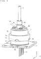
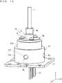
- FIG. 1is a perspective view of a light source device according to the first preferred embodiment
- FIG. 2is a perspective view of the light source device as viewed from a different direction
- FIG. 3is a Y-Z cross-sectional view in FIG. 1
- FIG. 4is an X-Z cross-sectional view in FIG. 1
- FIG. 5is an explanatory view of a shape of a light spot 15 converged on an optical fiber 1 of the light source device.
- the light source deviceincludes: a stem 11 (support base); a block 10; a laser diode (hereinafter referred to as "LD") 3 which constitutes an optical semiconductor element; a cap 6; a light converging lens 2 (light converging portion); an optical fiber 1; an optical fiber connection portion 16; and a holder 7.
- LDlaser diode
- the stem 11is a plate-shaped member for supporting the cap 6 and the block 10, and Au plating is applied to a surface of the stem 11.
- the block 10is arranged on an upper surface of the stem 11, and supports the light converging lens 2 and the LD 3 thereon.
- the LD 3is a multi-emitter laser diode, and is mounted on the stem 11. To be more specific, the LD 3 is mounted on a side portion of the block 10 arranged on the stem 11.
- a pin 12 for supplying electricity to the LD 3is connected to the LD 3 from the outside of the light source device.
- the light converging lens 2is mounted on the block 10 at a position above the LD 3, and converges light flux emitted from the LD 3 on the optical fiber 1.
- the cap 6is made of an Fe-Ni alloy and is formed into a cylindrical shape. Ni plating is applied to a surface of the cap 6.
- the cap 6is fixed to the upper surface of the stem 11 so as to cover the light converging lens 2 and the LD 3 mounted on the block 10.
- a lower end portion of the cap 6is bonded to the upper surface of the stem 11 by projection welding so that the inside of the cap 6 is airtightly sealed.
- a glass window 5which allows light emitted from the LD 3 to pass therethrough is arranged at a center portion of an upper surface of the cap 6.
- the holder 7is a member for holding the optical fiber connection portion 16, and is bonded to a side surface portion of the cap 6.
- the holder 7includes a large-diameter cylindrical portion 7a and a small-diameter cylindrical portion 7b arranged on an upper side of the large-diameter cylindrical portion 7a.
- a housing portion 7c for housing an upper portion of the cap 6is formed in an inner portion of a lower portion of the large-diameter cylindrical portion 7a
- a housing portion 7d for housing the glass window 5is formed in an inner portion of an upper portion of the large-diameter cylindrical portion 7a.
- the housing portion 7c and the housing portion 7dcommunicate with each other, and the housing portion 7c has a larger diameter than the housing portion 7d.
- a hole portion 7e which communicates with the housing portion 7dis formed at a center portion of the small-diameter cylindrical portion 7b.
- the optical fiber connection portion 16includes a receptacle 4 and a position adjusting portion 20 for adjusting a position of the optical fiber connection portion 16 with respect to the holder 7.
- the receptacle 4includes a disk portion 4a which is screw-fixed to the holder 7 using screws 9 and a connection portion 4b to which the optical fiber 1 is connected.
- the connection portion 4bis arranged at a center portion of the disk portion 4a. The detail of the position adjusting portion 20 is described later.
- a plurality of (four, for example) cut-away portions 7f to which adhesive agents 8a, 8b are appliedare formed on a lower end portion of the large-diameter cylindrical portion 7a.
- the adhesive agents 8a, 8bare members for adhesively fixing (bonding) the holder 7 and the cap 6 to each other.
- the adhesive agent 8ais an adhesive agent whose Young's modulus after curing is larger than Young's modulus of the adhesive agent 8b after curing.
- the LD 3is a multi-emitter-type laser diode and hence, the light spot 15 which is converged on the end surface 1a of the optical fiber 1 has a shape shown in FIG. 5 . Accordingly, transmissivity of the optical fiber 1 is easily changed in the longitudinal direction of the light spot 15, and transmissivity of the optical fiber 1 is hardly changed in the lateral direction of the light spot 15.
- the cut-away portions 7fare arranged at positions which are in line symmetry with respect to the center of an optical axis 13 of light flux emitted from the LD 3.
- the adhesive agents 8a, 8bare arranged at positions which are in line symmetry with respect to the center of the optical axis 13 of the light flux emitted from the LD 3.
- the adhesive agent 8ais applied to the cut-away portions 7f in the longitudinal direction of the light spot 15.
- the adhesive agent 8ahas larger Young's modulus after curing than Young's modulus of the adhesive agent 8b after curing and hence, a positional displacement of the holder 7 due to the adhesive agent 8a hardly occurs so that a positional displacement of the light spot 15 on the optical fiber 1 becomes small. Accordingly, it is possible to realize a highly reliable light source device.
- the adhesive agent 8b having smaller Young's modulus after curing than the adhesive agent 8ais applied to the cut-away portions 7f in the lateral direction of the light spot 15.
- the adhesive agent 8bhas a predetermined flexibility and hence, even when a heat cycle or the like is applied to the adhesive agent 8b, there is no possibility that the adhesive agent 8b ruptures whereby it is possible to acquire a reliable adhesive strength.
- the position adjusting portion 20which adjusts a position of the optical fiber connection portion 16 (to be more specific, receptacle 4) with respect to the holder 7 is described.
- the position adjusting portion 20includes the screws 9 and large-diameter holes 4c, and is configured such that the screws 9 are loosely fitted in the receptacle 4 with a play.
- the small-diameter cylindrical portion 7b of the holder 7 and the disk portion 4a of the receptacle 4are fixed to each other using the plurality of (three, for example) screws 9.
- a plurality of (three, for example) screw holes 7gare formed in an outer peripheral portion of the small-diameter cylindrical portion 7b, and a plurality of (three, for example) large-diameter holes 4c having a larger diameter than the screw holes 7g (in other words, a larger diameter than the shaft portion of the screw 9) are formed in an outer peripheral portion of the disk portion 4a.
- a predetermined gapis formed between the large-diameter hole 4c and the shaft portion of the screw 9 in a state where the screw 9 is inserted into the large-diameter hole 4c. Due to such a gap, the receptacle 4 is movable in the horizontal direction by an amount corresponding to the gap between the diameter of the large-diameter hole 4c and the diameter of the shaft portion of the screw 9.
- positions of the large-diameter holes 4c formed in the disk portions 4aare aligned to the screw holes 7g formed in the small-diameter cylindrical portions 7b and, in such a state, the screws 9 are fastened to the screw holes 7g halfway through the large-diameter holes 4c.
- the light converging lens 2is fixed to the block 10 with high accuracy using an adhesive agent such that light is converged on a predetermined target. Accordingly, a desired transmissivity can be acquired by merely performing the position adjustment of the receptacle 4 with respect to the holder 7. After the position adjustment of the receptacle 4 is performed, the screws 9 are fully fastened to the screw holes 7g. In such a state, the head portions of the screws 9 are brought in contact with the upper surface of the disk portion 4a and hence, the receptacle 4 is not movable in the horizontal direction. That is, the receptacle 4 is fixed to the holder 7.
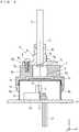
- FIG. 14is a cross-sectional view of the light source device according to the technique which is the premise of the present invention.
- the light source deviceincludes; a stem 107; an LD103; a cap 109; a light converging lens 102; an optical fiber 101; a ferrule 104; a ferrule holder 105; and a holder 106.
- the holder 106holds the light converging lens 102 and the ferrule holder 105 to which the optical fiber 101 is connected.
- the holder 106after the position adjustment is performed in a state where the holder 106 is brought into close contact with a stem 107 to which the LD 103 and a cap 109 are fixed, the holder 106 and the stem 107 are fixed by soldering or the like. Accordingly, a space for adjustment is required between the holder 106 and the cap 109 so that there has been a drawback that the structure of the holder 106 becomes complicated and the light source device becomes large-sized.
- the optical fiber connection portion 16includes the position adjusting portion 20 for adjusting the position of the optical fiber connection portion 16 with respect to the holder 7. Accordingly, the space for adjustment is unnecessary between the holder 7 and the cap 6 so that the structure of the holder 7 is simplified and, eventually, the light source device can be miniaturized.
- the position of the optical fiber connection portion 16 with respect to the holder 7can be adjusted using the position adjusting portion 20 and hence, the adjustment operation for converging light flux emitted from the LD 3 on the optical fiber 1 can be easily performed.
- the optical fiber connection portion 16includes a receptacle 4 which is screw-fixed to the holder 7 and to which the optical fiber 1 is connected.
- the position adjusting portion 20is configured such that screws 9 for the screw-fixing are loosely fitted in the receptacle 4 with a play. Accordingly, the receptacle 4 can be easily fixed to the holder 7 after performing the position adjustment of the receptacle 4. Further, the position adjusting portion 20 can be realized with the simple constitution.
- the light converging lens 2is arranged in the inside of the cap 6. To be more specific, the light converging lens 2 is bonded to the block 10 and hence, unlike the technique which is a premise of the present invention, it is no more necessary to impart a function as a lens holder for holding a light converging lens to the holder 7 whereby the light source device can be miniaturized and a manufacturing cost can be reduced.
- the LD 3is a multi-emitter laser diode so that the light converging lens 2 converges light flux emitted from the LD 3 on one point and hence, it is possible to increase a light output of the LD 3 having a plurality of light emitting points.
- the cap 6is formed into a cylindrical shape, and the holder 7 is bonded to a side surface portion of the cap 6.
- the adhesive agents 8a, 8b for bonding the holder 7 to the cap 6are arranged at positions which are in line symmetry with respect to the center of the optical axis 13 of light flux emitted from the LD 3 and hence, the holder 7 can be fixed to the cap 6 in a stable manner.
- the adhesive agents 8a, 8bare respectively arranged in the lateral direction and the longitudinal direction of the light spot 15 which is converged by the light converging lens 2, and the adhesive agent 8a arranged in the longitudinal direction of the light spot 15 has larger Young's modulus after curing than the adhesive agent 8b arranged in the lateral direction of the light spot 15.
- the adhesive agent 8bhas smaller Young's modulus after curing than the adhesive agent 8a so that the adhesive agent 8b has a higher flexibility than the adhesive agent 8a. Accordingly, even when a heat cycle or the like is applied to the adhesive agent 8b, the adhesive agent 8b hardly ruptures and hence, high adhesive strength can be acquired. As a result, the durability of the light source device can be enhanced.
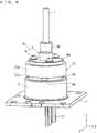
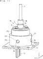
- FIG. 6is a perspective view of the light source device according to the second preferred embodiment
- FIG. 7is a perspective view of the light source device according to the second preferred embodiment as viewed from a different direction
- FIG. 8is a Y-Z cross-sectional view in FIG. 6
- FIG. 9is an X-Z cross-sectional view in FIG. 6 .
- constitutional elements identical with the corresponding constitutional elements described in the first preferred embodimentare given the same symbols, and the repeated explanation of these constitutional elements is omitted.
- the second preferred embodimentdiffers from the first preferred embodiment with respect to the structure of a holder.
- the light source deviceincludes a holder 27 in place of the holder 7 (see FIG. 1 ).
- the holder 27is formed in a cylindrical shape, and includes a small-diameter cylindrical portion 27a and a large-diameter cylindrical portion 27b arranged on an upper side of the small-diameter cylindrical portion 27a. A lower end of the small-diameter cylindrical portion 27a is bonded to an upper surface portion of a cap 6.
- the holder 27 and the cap 6are bonded to each other by applying adhesive agents 8a, 8b to a lower end portion of the small-diameter cylindrical portion 27a by coating.
- the positional relationship of the adhesive agents 8a, 8b in the small-diameter cylindrical portion 27ais substantially equal to the positional relationship of the adhesive agents 8a, 8b in the first preferred embodiment.
- a plurality of (three, for example) screw holes 27g to which screws 9 are fixedare formed in an outer peripheral portion of the large-diameter cylindrical portion 27b.
- a housing portion 27d in which a glass window 5 is housedis formed in an inner portion of the small-diameter cylindrical portion 27a.
- a hole portion 27e which communicates with the housing portion 27dis formed at a center portion of the large-diameter cylindrical portion 27b.
- the cap 6is formed into a cylindrical shape, and the holder 27 is bonded to the upper surface portion of the cap 6 and hence, compared to the light source device according to the first preferred embodiment, the holder 27 is miniaturized and the structure is simplified. Eventually, the light source device can be miniaturized.
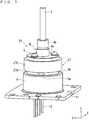
- FIG. 10is a perspective view of the light source device according to the third preferred embodiment
- FIG. 11is a perspective view of the light source device according to the third preferred embodiment as viewed from a different direction
- FIG. 12is a Y-Z cross-sectional view in FIG. 10
- FIG. 13is an X-Z cross-sectional view in FIG. 10 .
- constitutional elements identical with the corresponding constitutional elements described in the first and second preferred embodimentsare given the same symbols, and the repeated explanation of these constitutional elements is omitted.
- the light source deviceincludes a holder 37 in place of the holder 7 (see FIG. 1 ).
- the holder 37includes a large-diameter cylindrical portion 37a and a small-diameter cylindrical portion 37b arranged on an upper side of the large-diameter cylindrical portion 37a.
- a housing portion 37cis formed in an inner portion of the large-diameter cylindrical portion 37a.
- the housing portion 37cis configured so as to house a cap 6, and a lower end of the large-diameter cylindrical portion 37a is in contact with an upper surface of the stem 11 in a state where the holder 37 is fixed to the cap 6.
- a hole portion 37d which communicates with the housing portion 37cis formed at a center portion of the small-diameter cylindrical portion 37b.
- a plurality of (four, for example) window portions 37f to which adhesive agents 8a, 8b are appliedare formed on a side surface portion of the large-diameter cylindrical portion 37a.
- a plurality of (three, for example) screw holes 37g to which the screws 9 are fixedare formed in an outer peripheral portion of the small-diameter cylindrical portion 37b.
- the window portions 37fare formed at positions which are in line symmetry with respect to the center of the optical axis 13 of light flux emitted from the LD 3. Further, the positional relationship of the adhesive agents 8a, 8b in the large-diameter cylindrical portion 37a is substantially equal to the positional relationship of the adhesive agents 8a, 8b of the first preferred embodiment.
- the positioning of the holder 37 in the height directionis performed by bringing a lower end of the large-diameter cylindrical portion 37a of the holder 37 into contact with the upper surface of the stem 11. Further, the large-diameter cylindrical portion 37a is bonded to the side surface portion of the cap 6 by applying the adhesive agents 8a, 8b to the window portions 37f of the large-diameter cylindrical portion 37a. Accordingly, the LD 3 and the optical fiber 1 are positioned with higher accuracy and hence, the positional displacement of the light spot 15 when a fixing portion is displaced can be decreased.
Landscapes
- Physics & Mathematics (AREA)
- General Physics & Mathematics (AREA)
- Optics & Photonics (AREA)
- Engineering & Computer Science (AREA)
- General Engineering & Computer Science (AREA)
- Optical Couplings Of Light Guides (AREA)
- Semiconductor Lasers (AREA)
- Optical Head (AREA)
Description
- The present invention relates to a light source device which converges light flux emitted from a light source on an optical fiber.
US 2004/0114873 A1 discloses: An inexpensive, robust, and adhesive-free method and apparatus is disclosed for efficiently coupling first and second optical components together utilizing a flexure assembly for fine alignment. An initial three-dimensional rough alignment process positions the first and second optical components proximate to each other and aligns them in three dimensions. The first and second components are then misaligned by a fixed amount, causing a defocus, and then securely fastened together. The fine alignment process uses standard machine screws, or other easily attainable, robust tensioning means to progressively increase the tension around the periphery of the flexure assembly, which causes the flexure to bend and the second optical component to translate along the longitudinal axis of the flexure assembly and tilt with respect to the longitudinal axis of the flexure assembly, which refocuses and three-dimensionally finely aligns the optical components for optimum coupling efficiency in a simple and secure manner.US 2002/0168153 A1 discloses: An optical module with a small size and improved mass-productivity. The optical module comprises a fiber stub including an optical fiber, a sleeve containing the fiber stub, and a semiconductor optical amplifying device. A Bragg fiber grating is formed in the optical fiber. The optical fiber is secured in the ferrule. The optical amplifying device and the grating form a laser cavity. Only a part of the hollow portion of the sleeve is filled with a fiber stub. One end face of the optical fiber is disposed at one end of the sleeve. The other end of the sleeve is hollow. The optical module acts as an optical receptacle. An optical plug can be inserted into the hollow end of the sleeve. This enables the laser light to be introduced into an external optical device.- As a conventional light source device which converges light flux emitted from a light source on an optical fiber, there has been known a light source device where a light converging lens and a ferrule holder are held by a holder. In such a light source device, the positional adjustment of the holder is performed in a state where the holder is brought into close contact with a stem to which an optical semiconductor element and a cap are fixed and, thereafter, the holder and the stem are fixed to each other by soldering (see
Japanese Patent Application Laid-Open No. 2-32583 - In a conventional light source device used for optical communication, the holder and the stem are fixed to each other by soldering or the like using the above-mentioned method and hence, a space for adjustment is required between the holder and a cap. Accordingly, the conventional light source has a drawback that the structure of the holder becomes complicated and the light source device becomes large-sized.
- Further, it is necessary to fix the holder and the stem to each other by soldering or the like in a state where the positions of the holder and the stem are adjusted with high accuracy. Accordingly, there exist the following drawbacks. That is, when these constitutional members are heated and cooled at the time of performing fixing them by soldering, the constitutional members are thermally expanded and shrunken and a tension is generated in a soldered portion. Due to such thermal expansion or shrinkage of the constitutional members or the tension in the soldered portion, after fixing by soldering, the stem is positionally displaced from an optimum position by an order of micron thus giving rise to a drawback that a bonding efficiency is lowered exceeding an allowable level. Further, the conventional light source also has a drawback that the position adjustment operation of the holder with respect to the stem is difficult.
- The present invention is described in
independent claim 1. Aspects and advantages of the invention are as follows: - Provided is a technique by which the structure of a holder of a light source device can be simplified compared to prior art, the light source device can be miniaturized, and an adjustment operation for converging light flux emitted from a light source on an optical fiber can be performed easily.
- The light source device according to the present invention includes: an optical semiconductor element which is mounted on a support base; a cap which is fixed to the support base so as to cover the optical semiconductor element; a light converging portion which converges light flux emitted from the optical semiconductor element; an optical fiber connection portion to which an optical fiber is connected, the optical fiber receiving inputting of the light flux converged by the light converging portion; and a holder which holds the optical fiber connection portion, the holder being fixed to the cap. The optical fiber connection portion includes a position adjusting portion which adjusts a position of the optical fiber connection portion with respect to the holder.
- The optical fiber connection portion includes the position adjusting portion which adjusts the position of the optical fiber connection portion with respect to the holder. Accordingly, it is unnecessary to form a space for adjustment between the holder and the cap, and the holder can have the simplified structure so that the light source device can be miniaturized.
- Further, the position of the optical fiber connection portion with respect to the holder can be adjusted using the position adjusting portion and hence, an adjustment operation for converging light flux emitted from a light source on an optical fiber can be performed easily.
- These and other objects, features, aspects and advantages of the present invention will become more apparent from the following detailed description of the present invention when taken in conjunction with the accompanying drawings.
FIG. 1 is a perspective view of a light source device according to a first preferred embodiment;FIG. 2 is a perspective view of the light source device according to the first preferred embodiment as viewed from a different direction;FIG. 3 is a Y-Z cross-sectional view inFIG. 1 ;FIG. 4 is an X-Z cross-sectional view inFIG. 1 ;FIG. 5 is an explanatory view of a shape of a light spot converged on an optical fiber of the light source device according to the first preferred embodiment;FIG. 6 is a perspective view of a light source device according to a second preferred embodiment;FIG. 7 is a perspective view of the light source device according to the second preferred embodiment as viewed from a different direction;FIG. 8 is a Y-Z cross-sectional view inFIG. 6 ;FIG. 9 is an X-Z cross-sectional view inFIG. 6 ;FIG. 10 is a perspective view of a light source device according to a third preferred embodiment;FIG. 11 is a perspective view of the light source device according to the third preferred embodiment as viewed from a different direction;FIG. 12 is a Y-Z cross-sectional view inFIG. 10 ;FIG. 13 is an X-Z cross-sectional view inFIG. 10 ; andFIG. 14 is a cross-sectional view of a light source device according to a technique which is a premise of the present invention.- Hereinafter, a first preferred embodiment of the present invention is described by reference to drawings.
FIG. 1 is a perspective view of a light source device according to the first preferred embodiment,FIG. 2 is a perspective view of the light source device as viewed from a different direction,FIG. 3 is a Y-Z cross-sectional view inFIG. 1 ,FIG. 4 is an X-Z cross-sectional view inFIG. 1 , andFIG. 5 is an explanatory view of a shape of alight spot 15 converged on anoptical fiber 1 of the light source device. - As shown in
FIG. 1 to FIG. 4 , the light source device includes: a stem 11 (support base); ablock 10; a laser diode (hereinafter referred to as "LD") 3 which constitutes an optical semiconductor element; acap 6; a light converging lens 2 (light converging portion); anoptical fiber 1; an opticalfiber connection portion 16; and aholder 7. - The
stem 11 is a plate-shaped member for supporting thecap 6 and theblock 10, and Au plating is applied to a surface of thestem 11. Theblock 10 is arranged on an upper surface of thestem 11, and supports thelight converging lens 2 and theLD 3 thereon. The LD 3 is a multi-emitter laser diode, and is mounted on thestem 11. To be more specific, theLD 3 is mounted on a side portion of theblock 10 arranged on thestem 11. Apin 12 for supplying electricity to theLD 3 is connected to theLD 3 from the outside of the light source device. - The
light converging lens 2 is mounted on theblock 10 at a position above theLD 3, and converges light flux emitted from theLD 3 on theoptical fiber 1. Thecap 6 is made of an Fe-Ni alloy and is formed into a cylindrical shape. Ni plating is applied to a surface of thecap 6. Thecap 6 is fixed to the upper surface of thestem 11 so as to cover thelight converging lens 2 and theLD 3 mounted on theblock 10. A lower end portion of thecap 6 is bonded to the upper surface of thestem 11 by projection welding so that the inside of thecap 6 is airtightly sealed. Aglass window 5 which allows light emitted from theLD 3 to pass therethrough is arranged at a center portion of an upper surface of thecap 6. - Next, the
holder 7 is described. Theholder 7 is a member for holding the opticalfiber connection portion 16, and is bonded to a side surface portion of thecap 6. Theholder 7 includes a large-diametercylindrical portion 7a and a small-diametercylindrical portion 7b arranged on an upper side of the large-diametercylindrical portion 7a. Ahousing portion 7c for housing an upper portion of thecap 6 is formed in an inner portion of a lower portion of the large-diametercylindrical portion 7a, and ahousing portion 7d for housing theglass window 5 is formed in an inner portion of an upper portion of the large-diametercylindrical portion 7a. Thehousing portion 7c and thehousing portion 7d communicate with each other, and thehousing portion 7c has a larger diameter than thehousing portion 7d. Ahole portion 7e which communicates with thehousing portion 7d is formed at a center portion of the small-diametercylindrical portion 7b. - The optical
fiber connection portion 16 includes areceptacle 4 and aposition adjusting portion 20 for adjusting a position of the opticalfiber connection portion 16 with respect to theholder 7. Thereceptacle 4 includes adisk portion 4a which is screw-fixed to theholder 7 usingscrews 9 and aconnection portion 4b to which theoptical fiber 1 is connected. Theconnection portion 4b is arranged at a center portion of thedisk portion 4a. The detail of theposition adjusting portion 20 is described later. - In the inside of the
cap 6, divergent light is emitted from theLD 3 mounted on theblock 10, and the divergent light is converged by thelight converging lens 2 mounted on theblock 10. As indicated by anoptical path 14 inFIG. 3 andFIG. 4 , light flux which is converged by thelight converging lens 2 passes through theglass window 5 arranged in thecap 6 and, thereafter, is converged on anend surface 1a of theoptical fiber 1. - A plurality of (four, for example) cut-away
portions 7f to whichadhesive agents cylindrical portion 7a. Theadhesive agents holder 7 and thecap 6 to each other. Theadhesive agent 8a is an adhesive agent whose Young's modulus after curing is larger than Young's modulus of theadhesive agent 8b after curing. - By adhesively fixing the
holder 7 to thecap 6, it is possible to acquire highly-reliable adhesive strength compared to the case where theholder 7 is adhered to thestem 11 to which Au plating is applied. In this preferred embodiment, theLD 3 is a multi-emitter-type laser diode and hence, thelight spot 15 which is converged on theend surface 1a of theoptical fiber 1 has a shape shown inFIG. 5 . Accordingly, transmissivity of theoptical fiber 1 is easily changed in the longitudinal direction of thelight spot 15, and transmissivity of theoptical fiber 1 is hardly changed in the lateral direction of thelight spot 15. - The cut-away
portions 7f are arranged at positions which are in line symmetry with respect to the center of anoptical axis 13 of light flux emitted from theLD 3. In other words, theadhesive agents optical axis 13 of the light flux emitted from theLD 3. Theadhesive agent 8a is applied to the cut-awayportions 7f in the longitudinal direction of thelight spot 15. Theadhesive agent 8a has larger Young's modulus after curing than Young's modulus of theadhesive agent 8b after curing and hence, a positional displacement of theholder 7 due to theadhesive agent 8a hardly occurs so that a positional displacement of thelight spot 15 on theoptical fiber 1 becomes small. Accordingly, it is possible to realize a highly reliable light source device. - Further, the
adhesive agent 8b having smaller Young's modulus after curing than theadhesive agent 8a is applied to the cut-awayportions 7f in the lateral direction of thelight spot 15. Theadhesive agent 8b has a predetermined flexibility and hence, even when a heat cycle or the like is applied to theadhesive agent 8b, there is no possibility that theadhesive agent 8b ruptures whereby it is possible to acquire a reliable adhesive strength. - Next, the
position adjusting portion 20 which adjusts a position of the optical fiber connection portion 16 (to be more specific, receptacle 4) with respect to theholder 7 is described. Theposition adjusting portion 20 includes thescrews 9 and large-diameter holes 4c, and is configured such that thescrews 9 are loosely fitted in thereceptacle 4 with a play. - The small-diameter
cylindrical portion 7b of theholder 7 and thedisk portion 4a of thereceptacle 4 are fixed to each other using the plurality of (three, for example) screws 9. A plurality of (three, for example)screw holes 7g are formed in an outer peripheral portion of the small-diametercylindrical portion 7b, and a plurality of (three, for example) large-diameter holes 4c having a larger diameter than thescrew holes 7g (in other words, a larger diameter than the shaft portion of the screw 9) are formed in an outer peripheral portion of thedisk portion 4a. A predetermined gap is formed between the large-diameter hole 4c and the shaft portion of thescrew 9 in a state where thescrew 9 is inserted into the large-diameter hole 4c. Due to such a gap, thereceptacle 4 is movable in the horizontal direction by an amount corresponding to the gap between the diameter of the large-diameter hole 4c and the diameter of the shaft portion of thescrew 9. - Next, a method of adjusting a position of the
receptacle 4 using theposition adjusting portion 20 is described. Firstly, positions of the large-diameter holes 4c formed in thedisk portions 4a are aligned to thescrew holes 7g formed in the small-diametercylindrical portions 7b and, in such a state, thescrews 9 are fastened to the screw holes 7g halfway through the large-diameter holes 4c. In such a state, head portions of thescrews 9 are not brought into contact with the upper surface of thedisk portion 4a and hence, the position of thereceptacle 4 with respect to theholder 7 can be adjusted by merely moving thereceptacle 4 in the horizontal direction by an amount corresponding to the gap between the diameter of the large-diameter hole 4c and the diameter of the shaft portion of thescrew 9. - The
light converging lens 2 is fixed to theblock 10 with high accuracy using an adhesive agent such that light is converged on a predetermined target. Accordingly, a desired transmissivity can be acquired by merely performing the position adjustment of thereceptacle 4 with respect to theholder 7. After the position adjustment of thereceptacle 4 is performed, thescrews 9 are fully fastened to thescrew holes 7g. In such a state, the head portions of thescrews 9 are brought in contact with the upper surface of thedisk portion 4a and hence, thereceptacle 4 is not movable in the horizontal direction. That is, thereceptacle 4 is fixed to theholder 7. - Next, advantageous effects of the light source device according to the first preferred embodiment are described in comparison with the light source device which is a technique being the premise of the present invention. Firstly, the light source device according to the technique which is the premise of the present invention is simply described by reference to
FIG. 14. FIG. 14 is a cross-sectional view of the light source device according to the technique which is the premise of the present invention. - The light source device according to the technique which is the premise of the present invention includes; a
stem 107; an LD103; acap 109; alight converging lens 102; anoptical fiber 101; aferrule 104; aferrule holder 105; and aholder 106. Theholder 106 holds thelight converging lens 102 and theferrule holder 105 to which theoptical fiber 101 is connected. With respect to theholder 106, after the position adjustment is performed in a state where theholder 106 is brought into close contact with astem 107 to which theLD 103 and acap 109 are fixed, theholder 106 and thestem 107 are fixed by soldering or the like. Accordingly, a space for adjustment is required between theholder 106 and thecap 109 so that there has been a drawback that the structure of theholder 106 becomes complicated and the light source device becomes large-sized. - Further, it is necessary to fix the
holder 106 and thestem 107 to each other by soldering or the like at fixingportions 111 in a state where theholder 106 and thestem 107 are adjusted with high accuracy. Accordingly, there exist the following drawbacks. That is, when constitutional members are heated and cooled at the time of fixing them by soldering, the constitutional members are thermally expanded and shrunken and a tension is generated in a soldered portion. Due to such thermal expansion or shrinkage of the constitutional members or the tension in the soldered portion, after fixing by soldering, thestem 107 is displaced in position from an optimum position by an order of micron thus giving rise to a drawback that a bonding efficiency is lowered exceeding an allowable level. Further, the conventional light source also has a drawback that the position adjustment operation of theholder 106 with respect to thestem 107 is difficult. - To the contrary, in the light source device according to the first preferred embodiment, the optical
fiber connection portion 16 includes theposition adjusting portion 20 for adjusting the position of the opticalfiber connection portion 16 with respect to theholder 7. Accordingly, the space for adjustment is unnecessary between theholder 7 and thecap 6 so that the structure of theholder 7 is simplified and, eventually, the light source device can be miniaturized. - Further, the position of the optical
fiber connection portion 16 with respect to theholder 7 can be adjusted using theposition adjusting portion 20 and hence, the adjustment operation for converging light flux emitted from theLD 3 on theoptical fiber 1 can be easily performed. - The optical
fiber connection portion 16 includes areceptacle 4 which is screw-fixed to theholder 7 and to which theoptical fiber 1 is connected. Theposition adjusting portion 20 is configured such thatscrews 9 for the screw-fixing are loosely fitted in thereceptacle 4 with a play. Accordingly, thereceptacle 4 can be easily fixed to theholder 7 after performing the position adjustment of thereceptacle 4. Further, theposition adjusting portion 20 can be realized with the simple constitution. - The
light converging lens 2 is arranged in the inside of thecap 6. To be more specific, thelight converging lens 2 is bonded to theblock 10 and hence, unlike the technique which is a premise of the present invention, it is no more necessary to impart a function as a lens holder for holding a light converging lens to theholder 7 whereby the light source device can be miniaturized and a manufacturing cost can be reduced. - The
LD 3 is a multi-emitter laser diode so that thelight converging lens 2 converges light flux emitted from theLD 3 on one point and hence, it is possible to increase a light output of theLD 3 having a plurality of light emitting points. - The
cap 6 is formed into a cylindrical shape, and theholder 7 is bonded to a side surface portion of thecap 6. To be more specific, theadhesive agents holder 7 to thecap 6 are arranged at positions which are in line symmetry with respect to the center of theoptical axis 13 of light flux emitted from theLD 3 and hence, theholder 7 can be fixed to thecap 6 in a stable manner. - The
adhesive agents light spot 15 which is converged by thelight converging lens 2, and theadhesive agent 8a arranged in the longitudinal direction of thelight spot 15 has larger Young's modulus after curing than theadhesive agent 8b arranged in the lateral direction of thelight spot 15. - Accordingly, the positional displacement of the
holder 7 due to theadhesive agent 8a hardly occurs and hence, the positional displacement of thelight spot 15 on theoptical fiber 1 becomes small whereby it is possible to realize a highly reliable light source device. Further, theadhesive agent 8b has smaller Young's modulus after curing than theadhesive agent 8a so that theadhesive agent 8b has a higher flexibility than theadhesive agent 8a. Accordingly, even when a heat cycle or the like is applied to theadhesive agent 8b, theadhesive agent 8b hardly ruptures and hence, high adhesive strength can be acquired. As a result, the durability of the light source device can be enhanced. - Next, a light source device according to a second preferred embodiment is described.
FIG. 6 is a perspective view of the light source device according to the second preferred embodiment,FIG. 7 is a perspective view of the light source device according to the second preferred embodiment as viewed from a different direction,FIG. 8 is a Y-Z cross-sectional view inFIG. 6 , andFIG. 9 is an X-Z cross-sectional view inFIG. 6 . In the second preferred embodiment, constitutional elements identical with the corresponding constitutional elements described in the first preferred embodiment are given the same symbols, and the repeated explanation of these constitutional elements is omitted. - The second preferred embodiment differs from the first preferred embodiment with respect to the structure of a holder. As shown in
FIG. 6 to FIG. 9 , the light source device includes aholder 27 in place of the holder 7 (seeFIG. 1 ). Theholder 27 is formed in a cylindrical shape, and includes a small-diametercylindrical portion 27a and a large-diametercylindrical portion 27b arranged on an upper side of the small-diametercylindrical portion 27a. A lower end of the small-diametercylindrical portion 27a is bonded to an upper surface portion of acap 6. To be more specific, theholder 27 and thecap 6 are bonded to each other by applyingadhesive agents cylindrical portion 27a by coating. The positional relationship of theadhesive agents cylindrical portion 27a is substantially equal to the positional relationship of theadhesive agents - A plurality of (three, for example)
screw holes 27g to which screws 9 are fixed are formed in an outer peripheral portion of the large-diametercylindrical portion 27b. Ahousing portion 27d in which aglass window 5 is housed is formed in an inner portion of the small-diametercylindrical portion 27a. Ahole portion 27e which communicates with thehousing portion 27d is formed at a center portion of the large-diametercylindrical portion 27b. - As has been explained above, in the light source device according to the second preferred embodiment, the
cap 6 is formed into a cylindrical shape, and theholder 27 is bonded to the upper surface portion of thecap 6 and hence, compared to the light source device according to the first preferred embodiment, theholder 27 is miniaturized and the structure is simplified. Eventually, the light source device can be miniaturized. - Next, a light source device according to a third preferred embodiment is described.
FIG. 10 is a perspective view of the light source device according to the third preferred embodiment,FIG. 11 is a perspective view of the light source device according to the third preferred embodiment as viewed from a different direction,FIG. 12 is a Y-Z cross-sectional view inFIG. 10 , andFIG. 13 is an X-Z cross-sectional view inFIG. 10 . In the third preferred embodiment, constitutional elements identical with the corresponding constitutional elements described in the first and second preferred embodiments are given the same symbols, and the repeated explanation of these constitutional elements is omitted. - The third preferred embodiment differs from the first and second preferred embodiments with respect to the structure of a holder. As shown in
FIG. 10 to FIG. 13 , the light source device includes aholder 37 in place of the holder 7 (seeFIG. 1 ). Theholder 37 includes a large-diametercylindrical portion 37a and a small-diametercylindrical portion 37b arranged on an upper side of the large-diametercylindrical portion 37a. Ahousing portion 37c is formed in an inner portion of the large-diametercylindrical portion 37a. Thehousing portion 37c is configured so as to house acap 6, and a lower end of the large-diametercylindrical portion 37a is in contact with an upper surface of thestem 11 in a state where theholder 37 is fixed to thecap 6. - A
hole portion 37d which communicates with thehousing portion 37c is formed at a center portion of the small-diametercylindrical portion 37b. A plurality of (four, for example)window portions 37f to whichadhesive agents cylindrical portion 37a. A plurality of (three, for example)screw holes 37g to which thescrews 9 are fixed are formed in an outer peripheral portion of the small-diametercylindrical portion 37b. In this preferred embodiment, in the same manner as the cut-awayportions 7f in the first preferred embodiment, thewindow portions 37f are formed at positions which are in line symmetry with respect to the center of theoptical axis 13 of light flux emitted from theLD 3. Further, the positional relationship of theadhesive agents cylindrical portion 37a is substantially equal to the positional relationship of theadhesive agents - In the light source device according to the third preferred embodiment, the positioning of the
holder 37 in the height direction is performed by bringing a lower end of the large-diametercylindrical portion 37a of theholder 37 into contact with the upper surface of thestem 11. Further, the large-diametercylindrical portion 37a is bonded to the side surface portion of thecap 6 by applying theadhesive agents window portions 37f of the large-diametercylindrical portion 37a. Accordingly, theLD 3 and theoptical fiber 1 are positioned with higher accuracy and hence, the positional displacement of thelight spot 15 when a fixing portion is displaced can be decreased. - While the invention has been shown and described in detail, the foregoing description is in all aspects illustrative and not restrictive. It is therefore understood that numerous modifications and variations can be devised without departing from the scope of the invention.
Claims (5)
- A light source device comprising:an optical semiconductor element (3) which is mounted on a support base (11);a cap (6) which is fixed to said support base (11) so as to cover said optical semiconductor element (3);a light converging portion (2) which converges a light flux emitted from said optical semiconductor element (3);an optical fiber connection portion (16) to which an optical fiber (1) is connected, the optical fiber (1) receiving inputting of the light flux converged by said light converging portion (2); anda holder (7,27,37) which holds said optical fiber connection portion (16), the holder (7,27,37) being fixed to said cap (6), whereinsaid optical fiber connection portion (16) includes a position adjusting portion (20) which adjusts a position of said optical fiber connection portion (16) with respect to said holder (7,27,37),
characterized in that
said cap (6) is formed into a cylindrical shape and said holder (7, 27, 37) is bonded to a side surface portion or to an upper surface portion of said cap (6), and wherein adhesive agents (8a,8b) for bonding said holder (7,27,37) to said cap (6) are arranged at positions which are in line symmetry with respect to an optical axis of the light flux emitted from said optical semiconductor element (3). - The light source device according to claim 1, wherein
said adhesive agents (8a,8b) are arranged in a lateral direction and a longitudinal direction of a light spot converged by said light converging portion (2) respectively, and
said adhesive agent (8a) arranged in the longitudinal direction of said light spot has larger Young's modulus after curing than said adhesive agent (8b) arranged in the lateral direction of said light spot. - The light source device according to claim 1 or claim 2, wherein
said optical fiber connection portion (16) includes a receptacle (4) which is screw-fixed to said holder (7,27,37) and to which said optical fiber (1) is connected, and
said position adjusting portion (20) is configured such that a screw (9) for said screw-fixing is fitted in said receptacle (4) with a play. - The light source device according to any of claims 1 to 3, wherein
said light converging portion (2) is arranged in the inside of said cap (6). - The light source device according to any one of claims 1 to 4, wherein
said optical semiconductor element (3) is a multi-emitter type optical semiconductor element, and
said light converging portion (2) converges the light flux emitted from said optical semiconductor element (3) on one point.
Applications Claiming Priority (1)
| Application Number | Priority Date | Filing Date | Title |
|---|---|---|---|
| JP2013211749AJP2015075632A (en) | 2013-10-09 | 2013-10-09 | Light source device |
Publications (2)
| Publication Number | Publication Date |
|---|---|
| EP2860561A1 EP2860561A1 (en) | 2015-04-15 |
| EP2860561B1true EP2860561B1 (en) | 2016-12-21 |
Family
ID=51751888
Family Applications (1)
| Application Number | Title | Priority Date | Filing Date |
|---|---|---|---|
| EP14185341.6ANot-in-forceEP2860561B1 (en) | 2013-10-09 | 2014-09-18 | Light source device |
Country Status (5)
| Country | Link |
|---|---|
| US (1) | US9341793B2 (en) |
| EP (1) | EP2860561B1 (en) |
| JP (1) | JP2015075632A (en) |
| CN (1) | CN104565903B (en) |
| CA (1) | CA2863284C (en) |
Families Citing this family (5)
| Publication number | Priority date | Publication date | Assignee | Title |
|---|---|---|---|---|
| JP6926497B2 (en)* | 2017-02-03 | 2021-08-25 | 三菱電機株式会社 | Semiconductor optical module |
| JP6690610B2 (en)* | 2017-07-28 | 2020-04-28 | 日亜化学工業株式会社 | Light emitting device |
| CN111412438B (en)* | 2019-09-10 | 2022-09-27 | 深圳市海洋王冶金照明技术有限公司 | Light distribution positioning structure and flashlight |
| CN111425776B (en)* | 2019-09-10 | 2023-01-24 | 深圳市海洋王冶金照明技术有限公司 | Electric torch |
| JP7521458B2 (en)* | 2021-03-04 | 2024-07-24 | 住友電気工業株式会社 | Optical Connector Cable |
Family Cites Families (17)
| Publication number | Priority date | Publication date | Assignee | Title |
|---|---|---|---|---|
| NL7904283A (en)* | 1979-05-31 | 1980-12-02 | Philips Nv | COUPLING ELEMENT WITH A LIGHT SOURCE AND A LENS-SHAPED ELEMENT. |
| JPH0232583A (en) | 1988-07-22 | 1990-02-02 | Nippon Telegr & Teleph Corp <Ntt> | Semiconductor element module for optical communication |
| US5170454A (en)* | 1989-04-13 | 1992-12-08 | Kabushiki Kaisha Machida Seisakusho | Optical connector for endoscope |
| EP0412184B1 (en)* | 1989-08-09 | 1995-06-21 | Siemens Aktiengesellschaft | Optoelectronic converter with lens-coupling optics |
| NL9000027A (en) | 1990-01-05 | 1991-08-01 | Philips Nv | OPTO-ELECTRONIC DEVICE WITH A LENS COVERING BETWEEN AN OPTICAL TRANSMISSION FIBER AND A SEMICONDUCTOR LASER DIOD. |
| JPH04112211U (en)* | 1991-03-14 | 1992-09-30 | オムロン株式会社 | Optical semiconductor element coupling device |
| SE468150B (en) | 1991-05-06 | 1992-11-09 | Asea Brown Boveri | OPTION ELECTRONIC COMPONENT |
| JPH09205227A (en)* | 1996-01-25 | 1997-08-05 | Fujitsu Ltd | Optical semiconductor module |
| JP3495493B2 (en) | 1996-02-07 | 2004-02-09 | アルプス電気株式会社 | Light emitting module |
| JP4792656B2 (en) | 2001-05-09 | 2011-10-12 | 住友電気工業株式会社 | Optical module, fiber stub component |
| JP3748065B2 (en)* | 2002-02-14 | 2006-02-22 | 住友電気工業株式会社 | Optical fiber array |
| US6925234B2 (en)* | 2002-12-12 | 2005-08-02 | Melles Griot, Inc. | Flexure apparatus and method for achieving efficient optical coupling |
| JP2005165088A (en)* | 2003-12-04 | 2005-06-23 | Nec Compound Semiconductor Devices Ltd | Optical semiconductor device |
| JP2005215231A (en)* | 2004-01-29 | 2005-08-11 | Nippon Sheet Glass Co Ltd | Optical component and its manufacturing method |
| JP4741017B2 (en)* | 2008-09-22 | 2011-08-03 | 三菱電機株式会社 | Light source unit and image display device |
| JP5473534B2 (en)* | 2009-10-28 | 2014-04-16 | 三菱電機株式会社 | Light source device |
| JP5319624B2 (en)* | 2010-08-06 | 2013-10-16 | 日本電信電話株式会社 | Optical parts |
- 2013
- 2013-10-09JPJP2013211749Apatent/JP2015075632A/enactivePending
- 2014
- 2014-09-09USUS14/481,549patent/US9341793B2/ennot_activeExpired - Fee Related
- 2014-09-12CACA2863284Apatent/CA2863284C/ennot_activeExpired - Fee Related
- 2014-09-18EPEP14185341.6Apatent/EP2860561B1/ennot_activeNot-in-force
- 2014-10-09CNCN201410528416.0Apatent/CN104565903B/ennot_activeExpired - Fee Related
Non-Patent Citations (1)
| Title |
|---|
| None* |
Also Published As
| Publication number | Publication date |
|---|---|
| JP2015075632A (en) | 2015-04-20 |
| CA2863284C (en) | 2016-10-11 |
| CA2863284A1 (en) | 2015-04-09 |
| CN104565903B (en) | 2017-01-11 |
| US20150098241A1 (en) | 2015-04-09 |
| US9341793B2 (en) | 2016-05-17 |
| CN104565903A (en) | 2015-04-29 |
| EP2860561A1 (en) | 2015-04-15 |
Similar Documents
| Publication | Publication Date | Title |
|---|---|---|
| EP2860561B1 (en) | Light source device | |
| KR920010947B1 (en) | Optical coupling device and manufacturing method thereof, light emitting device and assembly method thereof, and lens holder | |
| JP6677654B2 (en) | Vision-based passive positioning of fiber optic subassemblies for optoelectronic devices | |
| KR0171374B1 (en) | Laser module with focusing lense and fixing method of the focusing lense | |
| KR100468130B1 (en) | An optoelectronic assembly and method for fabricating the same | |
| US20020126965A1 (en) | Semiconductor laser module and method for optically coupling laser light and optical fiber | |
| JP2008026462A (en) | Optical module | |
| JP2000277843A (en) | Semiconductor laser module and manufacture thereof | |
| CN101728761A (en) | Laser module including jointly arranged isolator and fiber sleeve | |
| JPH07134225A (en) | Sleeve integrated lens and optical coupling element module using this lens | |
| US6905354B1 (en) | U-clip for optical device alignment | |
| JP2007298643A (en) | Optical element module and manufacturing method thereof | |
| JP3907051B2 (en) | Optical module and manufacturing method thereof | |
| JP6898245B2 (en) | Optical bench subassembly with integrated optical device | |
| JP2004029161A (en) | Optical semiconductor device module | |
| US20060056778A1 (en) | Laser module with improved lens housing and associated methods | |
| JP2007333912A (en) | Optical module | |
| JPWO2007142089A1 (en) | Optical transmission module and manufacturing method thereof | |
| JP2005515621A (en) | Retaining device for placing optical components in front of a laser light source, and such a system, as well as a method for manufacturing such a system | |
| JPH0943455A (en) | Optical module | |
| JP2003075691A (en) | Optical assembly for opto-electronic package | |
| JP4514367B2 (en) | Semiconductor laser module and manufacturing method thereof | |
| JP2008040086A (en) | Optical fiber array | |
| JP4308049B2 (en) | Semiconductor element module | |
| JP2005309270A (en) | Optical module and manufacturing method thereof |
Legal Events
| Date | Code | Title | Description |
|---|---|---|---|
| PUAI | Public reference made under article 153(3) epc to a published international application that has entered the european phase | Free format text:ORIGINAL CODE: 0009012 | |
| 17P | Request for examination filed | Effective date:20140918 | |
| AK | Designated contracting states | Kind code of ref document:A1 Designated state(s):AL AT BE BG CH CY CZ DE DK EE ES FI FR GB GR HR HU IE IS IT LI LT LU LV MC MK MT NL NO PL PT RO RS SE SI SK SM TR | |
| AX | Request for extension of the european patent | Extension state:BA ME | |
| R17P | Request for examination filed (corrected) | Effective date:20150522 | |
| RBV | Designated contracting states (corrected) | Designated state(s):AL AT BE BG CH CY CZ DE DK EE ES FI FR GB GR HR HU IE IS IT LI LT LU LV MC MK MT NL NO PL PT RO RS SE SI SK SM TR | |
| GRAP | Despatch of communication of intention to grant a patent | Free format text:ORIGINAL CODE: EPIDOSNIGR1 | |
| INTG | Intention to grant announced | Effective date:20160706 | |
| GRAS | Grant fee paid | Free format text:ORIGINAL CODE: EPIDOSNIGR3 | |
| GRAA | (expected) grant | Free format text:ORIGINAL CODE: 0009210 | |
| AK | Designated contracting states | Kind code of ref document:B1 Designated state(s):AL AT BE BG CH CY CZ DE DK EE ES FI FR GB GR HR HU IE IS IT LI LT LU LV MC MK MT NL NO PL PT RO RS SE SI SK SM TR | |
| REG | Reference to a national code | Ref country code:GB Ref legal event code:FG4D | |
| REG | Reference to a national code | Ref country code:CH Ref legal event code:EP | |
| REG | Reference to a national code | Ref country code:IE Ref legal event code:FG4D | |
| REG | Reference to a national code | Ref country code:AT Ref legal event code:REF Ref document number:855971 Country of ref document:AT Kind code of ref document:T Effective date:20170115 | |
| REG | Reference to a national code | Ref country code:DE Ref legal event code:R096 Ref document number:602014005616 Country of ref document:DE | |
| PG25 | Lapsed in a contracting state [announced via postgrant information from national office to epo] | Ref country code:LV Free format text:LAPSE BECAUSE OF FAILURE TO SUBMIT A TRANSLATION OF THE DESCRIPTION OR TO PAY THE FEE WITHIN THE PRESCRIBED TIME-LIMIT Effective date:20161221 | |
| REG | Reference to a national code | Ref country code:LT Ref legal event code:MG4D | |
| REG | Reference to a national code | Ref country code:NL Ref legal event code:MP Effective date:20161221 | |
| PG25 | Lapsed in a contracting state [announced via postgrant information from national office to epo] | Ref country code:LT Free format text:LAPSE BECAUSE OF FAILURE TO SUBMIT A TRANSLATION OF THE DESCRIPTION OR TO PAY THE FEE WITHIN THE PRESCRIBED TIME-LIMIT Effective date:20161221 Ref country code:NO Free format text:LAPSE BECAUSE OF FAILURE TO SUBMIT A TRANSLATION OF THE DESCRIPTION OR TO PAY THE FEE WITHIN THE PRESCRIBED TIME-LIMIT Effective date:20170321 Ref country code:SE Free format text:LAPSE BECAUSE OF FAILURE TO SUBMIT A TRANSLATION OF THE DESCRIPTION OR TO PAY THE FEE WITHIN THE PRESCRIBED TIME-LIMIT Effective date:20161221 Ref country code:GR Free format text:LAPSE BECAUSE OF FAILURE TO SUBMIT A TRANSLATION OF THE DESCRIPTION OR TO PAY THE FEE WITHIN THE PRESCRIBED TIME-LIMIT Effective date:20170322 | |
| REG | Reference to a national code | Ref country code:AT Ref legal event code:MK05 Ref document number:855971 Country of ref document:AT Kind code of ref document:T Effective date:20161221 | |
| PG25 | Lapsed in a contracting state [announced via postgrant information from national office to epo] | Ref country code:HR Free format text:LAPSE BECAUSE OF FAILURE TO SUBMIT A TRANSLATION OF THE DESCRIPTION OR TO PAY THE FEE WITHIN THE PRESCRIBED TIME-LIMIT Effective date:20161221 Ref country code:FI Free format text:LAPSE BECAUSE OF FAILURE TO SUBMIT A TRANSLATION OF THE DESCRIPTION OR TO PAY THE FEE WITHIN THE PRESCRIBED TIME-LIMIT Effective date:20161221 Ref country code:RS Free format text:LAPSE BECAUSE OF FAILURE TO SUBMIT A TRANSLATION OF THE DESCRIPTION OR TO PAY THE FEE WITHIN THE PRESCRIBED TIME-LIMIT Effective date:20161221 | |
| PG25 | Lapsed in a contracting state [announced via postgrant information from national office to epo] | Ref country code:NL Free format text:LAPSE BECAUSE OF FAILURE TO SUBMIT A TRANSLATION OF THE DESCRIPTION OR TO PAY THE FEE WITHIN THE PRESCRIBED TIME-LIMIT Effective date:20161221 | |
| PG25 | Lapsed in a contracting state [announced via postgrant information from national office to epo] | Ref country code:CZ Free format text:LAPSE BECAUSE OF FAILURE TO SUBMIT A TRANSLATION OF THE DESCRIPTION OR TO PAY THE FEE WITHIN THE PRESCRIBED TIME-LIMIT Effective date:20161221 Ref country code:EE Free format text:LAPSE BECAUSE OF FAILURE TO SUBMIT A TRANSLATION OF THE DESCRIPTION OR TO PAY THE FEE WITHIN THE PRESCRIBED TIME-LIMIT Effective date:20161221 Ref country code:SK Free format text:LAPSE BECAUSE OF FAILURE TO SUBMIT A TRANSLATION OF THE DESCRIPTION OR TO PAY THE FEE WITHIN THE PRESCRIBED TIME-LIMIT Effective date:20161221 Ref country code:IS Free format text:LAPSE BECAUSE OF FAILURE TO SUBMIT A TRANSLATION OF THE DESCRIPTION OR TO PAY THE FEE WITHIN THE PRESCRIBED TIME-LIMIT Effective date:20170421 Ref country code:RO Free format text:LAPSE BECAUSE OF FAILURE TO SUBMIT A TRANSLATION OF THE DESCRIPTION OR TO PAY THE FEE WITHIN THE PRESCRIBED TIME-LIMIT Effective date:20161221 | |
| REG | Reference to a national code | Ref country code:FR Ref legal event code:PLFP Year of fee payment:4 | |
| PG25 | Lapsed in a contracting state [announced via postgrant information from national office to epo] | Ref country code:PT Free format text:LAPSE BECAUSE OF FAILURE TO SUBMIT A TRANSLATION OF THE DESCRIPTION OR TO PAY THE FEE WITHIN THE PRESCRIBED TIME-LIMIT Effective date:20170421 Ref country code:BG Free format text:LAPSE BECAUSE OF FAILURE TO SUBMIT A TRANSLATION OF THE DESCRIPTION OR TO PAY THE FEE WITHIN THE PRESCRIBED TIME-LIMIT Effective date:20170321 Ref country code:SM Free format text:LAPSE BECAUSE OF FAILURE TO SUBMIT A TRANSLATION OF THE DESCRIPTION OR TO PAY THE FEE WITHIN THE PRESCRIBED TIME-LIMIT Effective date:20161221 Ref country code:ES Free format text:LAPSE BECAUSE OF FAILURE TO SUBMIT A TRANSLATION OF THE DESCRIPTION OR TO PAY THE FEE WITHIN THE PRESCRIBED TIME-LIMIT Effective date:20161221 Ref country code:PL Free format text:LAPSE BECAUSE OF FAILURE TO SUBMIT A TRANSLATION OF THE DESCRIPTION OR TO PAY THE FEE WITHIN THE PRESCRIBED TIME-LIMIT Effective date:20161221 Ref country code:AT Free format text:LAPSE BECAUSE OF FAILURE TO SUBMIT A TRANSLATION OF THE DESCRIPTION OR TO PAY THE FEE WITHIN THE PRESCRIBED TIME-LIMIT Effective date:20161221 Ref country code:IT Free format text:LAPSE BECAUSE OF FAILURE TO SUBMIT A TRANSLATION OF THE DESCRIPTION OR TO PAY THE FEE WITHIN THE PRESCRIBED TIME-LIMIT Effective date:20161221 | |
| REG | Reference to a national code | Ref country code:DE Ref legal event code:R097 Ref document number:602014005616 Country of ref document:DE | |
| PLBE | No opposition filed within time limit | Free format text:ORIGINAL CODE: 0009261 | |
| STAA | Information on the status of an ep patent application or granted ep patent | Free format text:STATUS: NO OPPOSITION FILED WITHIN TIME LIMIT | |
| 26N | No opposition filed | Effective date:20170922 | |
| PG25 | Lapsed in a contracting state [announced via postgrant information from national office to epo] | Ref country code:DK Free format text:LAPSE BECAUSE OF FAILURE TO SUBMIT A TRANSLATION OF THE DESCRIPTION OR TO PAY THE FEE WITHIN THE PRESCRIBED TIME-LIMIT Effective date:20161221 | |
| PG25 | Lapsed in a contracting state [announced via postgrant information from national office to epo] | Ref country code:SI Free format text:LAPSE BECAUSE OF FAILURE TO SUBMIT A TRANSLATION OF THE DESCRIPTION OR TO PAY THE FEE WITHIN THE PRESCRIBED TIME-LIMIT Effective date:20161221 | |
| REG | Reference to a national code | Ref country code:CH Ref legal event code:PL | |
| PG25 | Lapsed in a contracting state [announced via postgrant information from national office to epo] | Ref country code:MC Free format text:LAPSE BECAUSE OF FAILURE TO SUBMIT A TRANSLATION OF THE DESCRIPTION OR TO PAY THE FEE WITHIN THE PRESCRIBED TIME-LIMIT Effective date:20161221 | |
| REG | Reference to a national code | Ref country code:IE Ref legal event code:MM4A | |
| PG25 | Lapsed in a contracting state [announced via postgrant information from national office to epo] | Ref country code:LU Free format text:LAPSE BECAUSE OF NON-PAYMENT OF DUE FEES Effective date:20170918 | |
| PG25 | Lapsed in a contracting state [announced via postgrant information from national office to epo] | Ref country code:IE Free format text:LAPSE BECAUSE OF NON-PAYMENT OF DUE FEES Effective date:20170918 Ref country code:LI Free format text:LAPSE BECAUSE OF NON-PAYMENT OF DUE FEES Effective date:20170930 Ref country code:CH Free format text:LAPSE BECAUSE OF NON-PAYMENT OF DUE FEES Effective date:20170930 | |
| REG | Reference to a national code | Ref country code:FR Ref legal event code:PLFP Year of fee payment:5 | |
| PG25 | Lapsed in a contracting state [announced via postgrant information from national office to epo] | Ref country code:MT Free format text:LAPSE BECAUSE OF NON-PAYMENT OF DUE FEES Effective date:20170918 | |
| PG25 | Lapsed in a contracting state [announced via postgrant information from national office to epo] | Ref country code:HU Free format text:LAPSE BECAUSE OF FAILURE TO SUBMIT A TRANSLATION OF THE DESCRIPTION OR TO PAY THE FEE WITHIN THE PRESCRIBED TIME-LIMIT; INVALID AB INITIO Effective date:20140918 | |
| PG25 | Lapsed in a contracting state [announced via postgrant information from national office to epo] | Ref country code:CY Free format text:LAPSE BECAUSE OF FAILURE TO SUBMIT A TRANSLATION OF THE DESCRIPTION OR TO PAY THE FEE WITHIN THE PRESCRIBED TIME-LIMIT Effective date:20161221 | |
| PG25 | Lapsed in a contracting state [announced via postgrant information from national office to epo] | Ref country code:MK Free format text:LAPSE BECAUSE OF FAILURE TO SUBMIT A TRANSLATION OF THE DESCRIPTION OR TO PAY THE FEE WITHIN THE PRESCRIBED TIME-LIMIT Effective date:20161221 | |
| PG25 | Lapsed in a contracting state [announced via postgrant information from national office to epo] | Ref country code:TR Free format text:LAPSE BECAUSE OF FAILURE TO SUBMIT A TRANSLATION OF THE DESCRIPTION OR TO PAY THE FEE WITHIN THE PRESCRIBED TIME-LIMIT Effective date:20161221 | |
| PG25 | Lapsed in a contracting state [announced via postgrant information from national office to epo] | Ref country code:AL Free format text:LAPSE BECAUSE OF FAILURE TO SUBMIT A TRANSLATION OF THE DESCRIPTION OR TO PAY THE FEE WITHIN THE PRESCRIBED TIME-LIMIT Effective date:20161221 | |
| PGFP | Annual fee paid to national office [announced via postgrant information from national office to epo] | Ref country code:DE Payment date:20200909 Year of fee payment:7 Ref country code:GB Payment date:20200909 Year of fee payment:7 Ref country code:FR Payment date:20200812 Year of fee payment:7 | |
| PGFP | Annual fee paid to national office [announced via postgrant information from national office to epo] | Ref country code:BE Payment date:20200817 Year of fee payment:7 | |
| REG | Reference to a national code | Ref country code:DE Ref legal event code:R119 Ref document number:602014005616 Country of ref document:DE | |
| REG | Reference to a national code | Ref country code:BE Ref legal event code:MM Effective date:20210930 | |
| GBPC | Gb: european patent ceased through non-payment of renewal fee | Effective date:20210918 | |
| PG25 | Lapsed in a contracting state [announced via postgrant information from national office to epo] | Ref country code:GB Free format text:LAPSE BECAUSE OF NON-PAYMENT OF DUE FEES Effective date:20210918 Ref country code:FR Free format text:LAPSE BECAUSE OF NON-PAYMENT OF DUE FEES Effective date:20210930 Ref country code:DE Free format text:LAPSE BECAUSE OF NON-PAYMENT OF DUE FEES Effective date:20220401 Ref country code:BE Free format text:LAPSE BECAUSE OF NON-PAYMENT OF DUE FEES Effective date:20210930 |