EP2846353B1 - Method of manufacturing a complementary metal oxide semiconductor device - Google Patents
Method of manufacturing a complementary metal oxide semiconductor deviceDownload PDFInfo
- Publication number
- EP2846353B1 EP2846353B1EP14183431.7AEP14183431AEP2846353B1EP 2846353 B1EP2846353 B1EP 2846353B1EP 14183431 AEP14183431 AEP 14183431AEP 2846353 B1EP2846353 B1EP 2846353B1
- Authority
- EP
- European Patent Office
- Prior art keywords
- layer
- type transistor
- manufacturing
- buffer layer
- pattern
- Prior art date
- Legal status (The legal status is an assumption and is not a legal conclusion. Google has not performed a legal analysis and makes no representation as to the accuracy of the status listed.)
- Active
Links
Images


Classifications
- H—ELECTRICITY
- H10—SEMICONDUCTOR DEVICES; ELECTRIC SOLID-STATE DEVICES NOT OTHERWISE PROVIDED FOR
- H10D—INORGANIC ELECTRIC SEMICONDUCTOR DEVICES
- H10D84/00—Integrated devices formed in or on semiconductor substrates that comprise only semiconducting layers, e.g. on Si wafers or on GaAs-on-Si wafers
- H10D84/01—Manufacture or treatment
- H10D84/02—Manufacture or treatment characterised by using material-based technologies
- H10D84/05—Manufacture or treatment characterised by using material-based technologies using Group III-V technology
- H—ELECTRICITY
- H10—SEMICONDUCTOR DEVICES; ELECTRIC SOLID-STATE DEVICES NOT OTHERWISE PROVIDED FOR
- H10D—INORGANIC ELECTRIC SEMICONDUCTOR DEVICES
- H10D84/00—Integrated devices formed in or on semiconductor substrates that comprise only semiconducting layers, e.g. on Si wafers or on GaAs-on-Si wafers
- H10D84/01—Manufacture or treatment
- H10D84/0123—Integrating together multiple components covered by H10D12/00 or H10D30/00, e.g. integrating multiple IGBTs
- H10D84/0126—Integrating together multiple components covered by H10D12/00 or H10D30/00, e.g. integrating multiple IGBTs the components including insulated gates, e.g. IGFETs
- H10D84/0165—Integrating together multiple components covered by H10D12/00 or H10D30/00, e.g. integrating multiple IGBTs the components including insulated gates, e.g. IGFETs the components including complementary IGFETs, e.g. CMOS devices
- H—ELECTRICITY
- H10—SEMICONDUCTOR DEVICES; ELECTRIC SOLID-STATE DEVICES NOT OTHERWISE PROVIDED FOR
- H10D—INORGANIC ELECTRIC SEMICONDUCTOR DEVICES
- H10D84/00—Integrated devices formed in or on semiconductor substrates that comprise only semiconducting layers, e.g. on Si wafers or on GaAs-on-Si wafers
- H10D84/01—Manufacture or treatment
- H10D84/02—Manufacture or treatment characterised by using material-based technologies
- H10D84/03—Manufacture or treatment characterised by using material-based technologies using Group IV technology, e.g. silicon technology or silicon-carbide [SiC] technology
- H10D84/038—Manufacture or treatment characterised by using material-based technologies using Group IV technology, e.g. silicon technology or silicon-carbide [SiC] technology using silicon technology, e.g. SiGe
- H—ELECTRICITY
- H10—SEMICONDUCTOR DEVICES; ELECTRIC SOLID-STATE DEVICES NOT OTHERWISE PROVIDED FOR
- H10D—INORGANIC ELECTRIC SEMICONDUCTOR DEVICES
- H10D84/00—Integrated devices formed in or on semiconductor substrates that comprise only semiconducting layers, e.g. on Si wafers or on GaAs-on-Si wafers
- H10D84/80—Integrated devices formed in or on semiconductor substrates that comprise only semiconducting layers, e.g. on Si wafers or on GaAs-on-Si wafers characterised by the integration of at least one component covered by groups H10D12/00 or H10D30/00, e.g. integration of IGFETs
- H10D84/82—Integrated devices formed in or on semiconductor substrates that comprise only semiconducting layers, e.g. on Si wafers or on GaAs-on-Si wafers characterised by the integration of at least one component covered by groups H10D12/00 or H10D30/00, e.g. integration of IGFETs of only field-effect components
- H10D84/83—Integrated devices formed in or on semiconductor substrates that comprise only semiconducting layers, e.g. on Si wafers or on GaAs-on-Si wafers characterised by the integration of at least one component covered by groups H10D12/00 or H10D30/00, e.g. integration of IGFETs of only field-effect components of only insulated-gate FETs [IGFET]
- H10D84/8311—Integrated devices formed in or on semiconductor substrates that comprise only semiconducting layers, e.g. on Si wafers or on GaAs-on-Si wafers characterised by the integration of at least one component covered by groups H10D12/00 or H10D30/00, e.g. integration of IGFETs of only field-effect components of only insulated-gate FETs [IGFET] the IGFETs characterised by having different channel structures
- H—ELECTRICITY
- H10—SEMICONDUCTOR DEVICES; ELECTRIC SOLID-STATE DEVICES NOT OTHERWISE PROVIDED FOR
- H10D—INORGANIC ELECTRIC SEMICONDUCTOR DEVICES
- H10D84/00—Integrated devices formed in or on semiconductor substrates that comprise only semiconducting layers, e.g. on Si wafers or on GaAs-on-Si wafers
- H10D84/80—Integrated devices formed in or on semiconductor substrates that comprise only semiconducting layers, e.g. on Si wafers or on GaAs-on-Si wafers characterised by the integration of at least one component covered by groups H10D12/00 or H10D30/00, e.g. integration of IGFETs
- H10D84/82—Integrated devices formed in or on semiconductor substrates that comprise only semiconducting layers, e.g. on Si wafers or on GaAs-on-Si wafers characterised by the integration of at least one component covered by groups H10D12/00 or H10D30/00, e.g. integration of IGFETs of only field-effect components
- H10D84/83—Integrated devices formed in or on semiconductor substrates that comprise only semiconducting layers, e.g. on Si wafers or on GaAs-on-Si wafers characterised by the integration of at least one component covered by groups H10D12/00 or H10D30/00, e.g. integration of IGFETs of only field-effect components of only insulated-gate FETs [IGFET]
- H10D84/85—Complementary IGFETs, e.g. CMOS
- H—ELECTRICITY
- H10—SEMICONDUCTOR DEVICES; ELECTRIC SOLID-STATE DEVICES NOT OTHERWISE PROVIDED FOR
- H10D—INORGANIC ELECTRIC SEMICONDUCTOR DEVICES
- H10D84/00—Integrated devices formed in or on semiconductor substrates that comprise only semiconducting layers, e.g. on Si wafers or on GaAs-on-Si wafers
- H10D84/01—Manufacture or treatment
- H10D84/02—Manufacture or treatment characterised by using material-based technologies
- H10D84/08—Manufacture or treatment characterised by using material-based technologies using combinations of technologies, e.g. using both Si and SiC technologies or using both Si and Group III-V technologies
Definitions
- CMOScomplementary metal oxide semiconductor
- Group III-V semiconductor materialsSince the electron mobility of Group III-V compound semiconductor materials is higher by about 10 times to about 10 3 times than the electron mobility of silicon (Si), the Group III-V compound semiconductor materials are used for high-speed channels in complementary metal oxide semiconductor (CMOS) devices or are suitably applied to high-efficiency Group III-V solar cells.
- CMOScomplementary metal oxide semiconductor
- the Group III-V substratesare more expensive and more likely to be damaged during a process than Si substrates.
- the maximum size of commercial substratesis about 6 inches, and the Group III-V substrates are difficult to manufacture in large sizes.
- semiconductor devices using Si substrates instead of Group III-V substrateshave been developed.
- US 2013/0062696 and US 2013/0246409describe methods of preparing a SOI semiconductor structure with a hybrid of coplanar Ge and III-V.
- a first aspect of the inventionrelates to methods of manufacturing CMOS devices including both an n-type transistor layer and a p-type transistor layer on a silicon substrate according to claim 1.
- a CMOS deviceincludes a silicon substrate; a buffer layer on the silicon substrate; a first layer for an n-type transistor on the buffer layer; a second layer for a p-type transistor disposed on the buffer layer or the silicon substrate while being spaced apart from the first layer; and an insulating layer between the first layer and the second layer.
- At least one example embodimentincludes a method of manufacturing a complementary metal oxide semiconductor (CMOS) device that includes forming a buffer layer on a substrate, forming a first material layer on the buffer layer, the first material layer including a group III-V material, etching the first material layer to form a first layer and a first pattern, forming an insulating layer on the first layer and the first pattern, etching the insulating layer to form a second pattern, and selectively growing a second material layer in the second pattern, the second material layer including a group IV material.
- CMOScomplementary metal oxide semiconductor
- a method of manufacturing a complementary metal oxide semiconductor (CMOS) deviceincludes forming a buffer layer on a silicon substrate; forming a material layer for an n-type transistor on the buffer layer; etching the material layer for the n-type transistor to form a first layer for the n-type transistor and a first pattern; forming an insulating layer on the first layer and the first pattern; etching the insulating layer to form a second pattern for selective growth; and selectively growing a second layer for a p-type transistor in the second pattern.
- CMOScomplementary metal oxide semiconductor
- the buffer layermay include or, alternatively, be formed of a Group III-V material including at least one selected from the group consisting of indium (In), gallium (Ga), and aluminum (Al), and at least one selected from the group consisting of arsenic (As), phosphorus (P), and antimony (Sb).
- a Group III-V materialincluding at least one selected from the group consisting of indium (In), gallium (Ga), and aluminum (Al), and at least one selected from the group consisting of arsenic (As), phosphorus (P), and antimony (Sb).
- the buffer layermay include or, alternatively, be formed of at least one selected from the group consisting of InP, InAs, InSb, GaAs, GaP, GaSb, AlP, AlAs, AlSb, InAlAs, InGaP, GaAsP, InGaAsP, and InGaAlAs.
- the buffer layermay be doped with an n-type dopant.
- the buffer layermay include at least one Group IV material.
- the buffer layermay include or, alternatively, be formed of at least one of SiGe, GeSn, and germanium (Ge).
- the first layermay include or, alternatively, be formed of a Group III-V material.
- the first layermay include or, alternatively, be formed of at least one of InGaAs, InP, InSb, InGaSb, GaSb, and InAs.
- the second layermay include or, alternatively, be formed of a Group IV material.
- the second layermay include or, alternatively, be formed of Ge.
- the n-type transistormay include an n-type metal oxide semiconductor field effect transistor (MOSFET).
- MOSFETmetal oxide semiconductor field effect transistor
- the p-type transistormay include a p-type MOSFET.
- the first layer and the second layermay be channel layers.
- the material layermay be etched to expose a portion of the buffer layer.
- the material layermay be etched to expose the silicon substrate.
- the insulating layermay include or, alternatively, be formed of a silicon oxide film, a silicon nitride film, or a silicon oxynitride film.
- CMOScomplementary metal oxide semiconductor
- first, second, etc.may be used herein to describe various elements, components, regions, layers and/or sections, these elements, components, regions, layers and/or sections should not be limited by these terms. These terms are only used to distinguish one element, component, region, layer or section from another element, component, region, layer or section. Thus, a first element, component, region, layer or section discussed below could be termed a second element, component, region, layer or section without departing from the teachings of example embodiments.
- spatially relative termssuch as “beneath,” “below,” “lower,” “above,” “upper” and the like, may be used herein for ease of description to describe one element or feature's relationship to another element(s) or feature(s) as illustrated in the figures. It will be understood that the spatially relative terms are intended to encompass different orientations of the device in use or operation in addition to the orientation depicted in the figures. For example, if the device in the figures is turned over, elements described as “below” or “beneath” other elements or features would then be oriented “above” the other elements or features. Thus, the example term “below” can encompass both an orientation of above and below. The device may be otherwise oriented (rotated 90 degrees or at other orientations) and the spatially relative descriptors used herein interpreted accordingly.
- Example embodimentsare described herein with reference to cross-sectional illustrations that are schematic illustrations of idealized embodiments (and intermediate structures) of example embodiments. As such, variations from the shapes of the illustrations as a result, for example, of manufacturing techniques and/or tolerances, are to be expected. Thus, example embodiments should not be construed as limited to the particular shapes of regions illustrated herein but are to include deviations in shapes that result, for example, from manufacturing. For example, an implanted region illustrated as a rectangle will, typically, have rounded or curved features and/or a gradient of implant concentration at its edges rather than a binary change from implanted to non-implanted region.
- a buried region formed by implantationmay result in some implantation in the region between the buried region and the surface through which the implantation takes place.
- the regions illustrated in the figuresare schematic in nature and their shapes are not intended to illustrate the actual shape of a region of a device and are not intended to limit the scope of example embodiments.
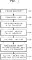
- FIG. 1is a flowchart illustrating a CMOS device manufacturing method according to an example embodiment.
- a substrateis prepared S10, and a buffer layer is formed on the substrate S20.
- the substratemay be a silicon-based substrate.
- the substratemay be a silicon substrate.
- a first layer for an n-type transistoris grown on the buffer layer S30.
- the n-type transistormay be an n-type metal oxide semiconductor field effect transistor (MOSFET).
- MOSFETmetal oxide semiconductor field effect transistor
- the first layer for the n-type transistoris etched to form a first pattern S40.
- the first patternmay expose a portion of the buffer layer or may expose a portion of the substrate.
- An insulating layeris stacked on the first layer for the n-type transistor and the first pattern S50.
- the insulating layeris etched to form a second pattern for selective growth S60.
- the second patternmay be a pattern for selectively growing a second layer for a p-type transistor.
- a second layer for a p-type transistoris formed in the second pattern S70.
- the p-type transistormay be a p-type MOSFET.
- the first layer for the n-type transistormay be formed of a material with high electron mobility
- the second layer for the p-type transistormay be formed of a material with high hole mobility.
- the example embodimentprovides a manufacturing method that may form both an n-type transistor and a p-type transistor on one substrate.
- FIGS. 2 to 8illustrate a CMOS device manufacturing method according to an example embodiment.
- a buffer layer 13may be formed on a substrate 10, and a material layer 15 for an n-type transistor may be formed on the buffer layer 13.
- the substrate 10may be a silicon-based substrate.
- the substrate 10may be doped with a p-type or n-type dopant.
- the substrate 10may be a silicon substrate, and may be a p-type silicon substrate.
- the material layer 15 for the n-type transistormay be formed of a Group III-V material, which will be described later.
- the buffer layer 13may be formed of a Group III-V material of the same series as the material layer 15.
- the buffer layer 13may include a Group III-V material including at least one selected from the group consisting of indium (In), gallium (Ga), and aluminum (Al), and at least one selected from the group consisting of arsenic (As), phosphorus (P), and antimony (Sb).
- the Group III-V material for the buffer layer 13may be a two-element material, a three-element material, or a four-element material.
- the two-element materialmay be InP, InAs, InSb, GaAs, GaP, GaSb, AlP, AlAs, or AlSb.
- the three-element materialmay be InAlAs, InGaP, or GaAsP.
- the four-element materialmay be InGaAsP or InGaAlAs.
- the buffer layer 13may be an n-type material layer.
- the buffer layer 13may be a layer doped with an n-type dopant, or may be a layer having an n-type doping effect.
- the buffer layer 13may be an n-InP layer.
- the buffer layer 13may reduce the lattice constant difference and the thermal expansion coefficient difference between the substrate 10 and the material layer 15 for the n-type transistor and reduce the defects thereof to increase the crystallinity of the material layer 15 of the n-type transistor.
- the buffer layer 13may be formed of a material of the same series as a material for a second layer 25 for a p-type transistor, which will be described later.
- the buffer layer 13may be formed of at least one Group IV material.
- the buffer layer 13may include at least one of SiGe, GeSn, and Ge.
- the material layer 15 for the n-type transistormay be formed of a Group III-V material.
- the III-V materialmay include at least one of InGaAs, InP, InSb, InGaSb, GaSb, and InAs.
- the material layer 15 for the n-type transistormay have a quantum well structure.
- a wet treatment or in-situ annealingmay be performed as a pretreatment on the material layer 15 of the n-type transistor.
- the n-type transistormay be an n-type MOSFET.
- the material layer 15 for the n-type transistormay be etched to form a first layer 17 for the n-type transistor and a first pattern 18.
- the first layer 17may be a channel layer of the n-type transistor.
- the first pattern 18may expose a portion of the buffer layer 13.
- the material layer 15 for the n-type transistormay be etched by using photoresist.
- an insulating layer 20may be formed on the first layer 17 for the n-type transistor and an exposed region of the buffer layer 13.
- the insulating layer 20may be formed of an oxide film, a nitride film, or an oxynitride film.
- the insulating layer 20may be formed of a silicon oxide (SiO 2 ) film, a silicon nitride (SiN x ) film, or a silicon oxynitride (SiO x N y ) film. Referring to FIG.
- the insulating layer 20may be etched to form a second pattern 23 for selective growth.
- a second layer 25 for a p-type transistormay be formed in the second pattern 23 by selective growth.
- the second layer 25may be grown to have a thickness that is smaller than, equal to, or greater than the depth of the second pattern 23.
- the surface of the second layer 25may be planarized through a planarization process.
- the planarization processmay be a chemical mechanical polishing (CMP) process.
- CMPchemical mechanical polishing
- the planarization processis not mandatory but may be performed selectively according to the surface state of the second layer 25.
- the insulating layer 20may be used as a mask in the selective growth process.
- the second layer 25may be formed of a material including a Group IV material.
- the second layer 25may be formed of germanium (Ge).
- the second layer 25may be grown by epitaxial growth.
- the second layer 25may be formed by growing germanium to several tens of nm at a low temperature of, for example, about 400°C, and then growing germanium at a high temperature of, for example, about 600°C.
- the insulating layer 20may be used as a mask. Since the surface of the first layer 17 is covered with the insulating layer 20, the second layer 25 may be selectively grown on the exposed region of the buffer layer 13.
- the surface of the resulting structure illustrated in FIG. 6may be planarized to expose the first layer 17.
- the planarizationmay be performed through a CMP process.
- both the first layer 17 for the n-type transistor and the second layer 25 for the p-type transistormay be formed on one substrate 10.
- selectively growing the second layer 25 formed of a Ge materialmay be easier and simpler than selectively growing the first layer 17 formed of a Group III-V material.
- a first source electrode S1 and a first drain electrode D1may be formed at both sides of the first layer 17.
- the first source electrode S1 and the first drain electrode D1may be formed at a top portion of the first layer 17 while being spaced apart from each other.
- a second source electrode S2 and a second drain electrode D2may be formed at both sides of the second layer 25.
- the second source electrode S2 and the second drain electrode D2may be formed at a top portion of the second layer 25 while being spaced apart from each other.
- the first and second source electrodes S1 and S2 and the first and second drain electrodes D1 and D2may be formed by implantation.
- the source electrodes and the drain electrodesmay be formed by various other methods.
- the first and second source electrodes S1 and S2 and the first and second drain electrodes D1 and D2may be formed of a conductive material, for example, a metal or an alloy.
- the first and second source electrodes S1 and S2 and the first and second drain electrodes D1 and D2may be formed of a Ti/Au alloy or a Ge/Au/Ni/Au alloy.
- a first gate insulating layer 30may be formed on the first layer 17, and a second gate insulating layer 40 may be formed on the second layer 25.
- the first and second gate insulating layers 30 and 40may include at least one of Al 2 O 3 , SiO x , Si x N y , Sc 2 O 3 , AlN, Ga 2 O 3 , Gd 2 O 3 , Al x Ga 2(1-x) O 3 , and MgO.
- example embodimentsare not limited thereto, and the first and second gate insulating layers 30 and 40 may include any gate insulating layer material that is used in a general transistor.
- a first gate electrode G1may be formed on the first gate insulating layer 30, and a second gate electrode G2 may be formed on the second gate insulating layer 40.
- a first spacer 33may be formed on both sides of the first gate electrode G1.
- a second spacer 43may be formed on both sides of the second gate electrode G2.
- the first gate electrode G1, the first source electrode S1, and the first drain electrode D1may be formed of various metals or conductive oxide materials. Also, the first gate electrode G1, the first source electrode S1, and the first drain electrode D1 may be formed of the same material, or may be formed of different materials.
- the second gate electrode G2, the second source electrode S2, and the second drain electrode D2may be formed of various metals or conductive oxide materials.
- the second gate electrode G2, the second source electrode S2, and the second drain electrode D2may be formed of the same material, or may be formed of different materials. Since the first and second gate insulating layers 30 and 40 have a very large energy bandgap, the first and second gate insulating layers 30 and 40 may function as barrier layers with respect to the first and second layers 17 and 25, respectively.
- a CMOS deviceincludes a substrate 10, a buffer layer 13 on the substrate 10, and a first layer 17 for an n-type transistor and a second layer 25 for a p-type transistor that are disposed on the buffer layer while being spaced apart from each other. Also, an insulating layer 20 may be provided between the first layer 17 and the second layer 25. Accordingly, the CMOS device includes both the first layer 17 for the n-type transistor and the second layer 25 for the p-type transistor, on one substrate 10.
- FIGS. 9 to 15illustrate a CMOS device manufacturing method according to another example embodiment.
- a buffer material layer 113may be formed on a substrate 110, and a material layer 115 for an n-type transistor may be formed on the buffer material layer 113.
- the substrate 110may be a silicon-based substrate.
- the substrate 110may be doped with a p-type or n-type dopant.
- the substrate 110may be a silicon substrate, and may be a p-type silicon substrate.
- the material layer 115 for the n-type transistormay be formed of a Group III-V material.
- the buffer material layer 113may be formed of a Group III-V material of the same series as the material layer 115 for the n-type transistor. Since the buffer material layer 113 and the material layer 115 for the n-type transistor may be formed of the same materials and may perform the same operations as the buffer layer 13 and the material layer 15 of the n-type transistor described with reference to FIGS. 2 to 8 , detailed descriptions thereof will be omitted herein.
- the material layer 115 for the n-type transistor and the buffer material layer 113may be etched to form a first layer 117 for the n-type transistor, a buffer layer 114 and a first pattern 118.
- the first pattern 118may expose a portion of the substrate 110.
- an insulating layer 120may be formed on the first layer 117 for the n-type transistor and an exposed region of the substrate 110.
- the insulating layer 120may be formed of an oxide film, a nitride film, or an oxynitride film.
- the insulating layer 120may be formed of a silicon oxide (SiO 2 ) film, a silicon nitride (SiN x ) film, or a silicon oxynitride (SiO x N y ) film.
- the insulating layer 120may be etched to form a second pattern 123 for selective growth.
- the second pattern 123may expose a portion of the substrate 110.
- a second layer 125 for a p-type transistormay be formed in the second pattern 123 by selective growth.
- the insulating layer 120may be used as a mask in the selective growth process.
- the second layer 125may be formed of a material including a Group IV material.
- the second layer 125may be formed of germanium (Ge). Since the surface of the first layer 117 is covered with the insulating layer 120, the second layer 125 may be selectively grown on the exposed region of the substrate 110.
- the surfaces of the first layer 117 and the second layer 125may be planarized through a planarization process. Accordingly, both the first layer 117 for the n-type transistor and the second layer 125 for the p-type transistor may be formed on one substrate 110. For example, selectively growing the second layer 125 formed of a single material may be easier and simpler than selectively growing the first layer 117 formed of a Group III-V compound material.
- a first source electrode S11 and a first drain electrode D11may be formed at both sides of the first layer 117.
- the first source electrode S11 and the first drain electrode D11may be formed at a top portion of the first layer 117 while being spaced apart from each other.
- a second source electrode S12 and a second drain electrode D12may be formed at both sides of the second layer 125.
- a first spacer 133may be formed on both sides of a first gate electrode G11.
- a second spacer 143may be formed on both sides of a second gate electrode G12.
- the second source electrode S12 and the second drain electrode D12may be formed at a top portion of the second layer 125 while being spaced apart from each other.
- a first gate insulating layer 130may be formed on the first layer 117, and the first gate electrode G11 may be formed on the first gate insulating layer 130.
- a second gate insulating layer 140may be formed on the second layer 125, and the second gate electrode G12 may be formed on the second gate insulating layer 140.
- a buffer layer 114may be provided on a substrate 110, a first layer 117 for an n-type transistor may be provided on the buffer layer 114, and a second layer 125 for a p-type transistor may be provided on the substrate 110 while being spaced apart from the first layer 117. Also, an insulating layer 120 may be provided between the first layer 117 and the second layer 125.
- FIGS. 16 to 23illustrate a CMOS device manufacturing method according to another example embodiment.
- a substrate 210is prepared. Referring to FIG. 17 , the substrate 210 is etched to form a first pattern 212. Referring to FIG. 18 , a buffer layer 213 and a material layer 215 for an n-type transistor are formed in the first pattern 212. Referring to FIG. 19 , the material layer 215 for the n-type transistor is etched to form a first layer 217 for the n-type transistor and a second pattern 218. The second pattern 218 may be formed to expose the buffer layer 213 or to expose the substrate 210. FIG. 19 illustrates an example in which the buffer layer 213 is exposed.
- an insulating layer 220is formed on the resulting structure illustrated in FIG. 19 .
- the insulating layer 220may be etched to form a third pattern 223.
- the third pattern 223may be a pattern for selective growth.
- a second layer 225 for a p-type transistormay be selectively grown in the third pattern 223.
- the insulating layer 220may be used as a mask in the selective growth.
- the surfaces of the substrate 210, the first layer 217, and the second layer 225may be planarized through a planarization process. Since the components using the same denotations as the components described with reference to FIGS. 2 and 8 may be formed of the same materials and may perform the same functions and operations as the corresponding components of FIGS. 2 and 8 , detailed description thereof will be omitted herein.
- FIG. 24illustrates an example in which a first region 310, a second region 320, and a third region 330 are included in one cell 305 of a wafer 300.
- the first region 310may be a silicon region 310
- the second region 320may be a Group III-V compound region
- the third region 330may be a Ge region.
- a photonic devicemay be provided in the first region 310
- an n-type transistormay be provided in the second region 320
- a p-type transistormay be provided in the third region 330.
- the photonic devicemay be a light emitting diode (LED), a laser diode (LD), or a photodiode (PD).
- the n-type transistor and the p-type transistormay operate as an electronic device that supports a light-emitting or light-receiving operation of the photonic device. Also, in this way, photonic device integration and hybrid electronic and photonic circuit integration may be possible.
Landscapes
- Metal-Oxide And Bipolar Metal-Oxide Semiconductor Integrated Circuits (AREA)
Description
- The present disclosure relates to complementary metal oxide semiconductor (CMOS) devices and/or methods of manufacturing the same, and more particularly, to CMOS devices including both an n-type transistor layer and a p-type transistor layer on a silicon substrate and/or methods of manufacturing the same.
- Extensive research has been conducted to develop devices that use compound semiconductors, for example, Group III-V semiconductor materials. Since the electron mobility of Group III-V compound semiconductor materials is higher by about 10 times to about 103 times than the electron mobility of silicon (Si), the Group III-V compound semiconductor materials are used for high-speed channels in complementary metal oxide semiconductor (CMOS) devices or are suitably applied to high-efficiency Group III-V solar cells.
- Group III-V substrates formed of materials, such as InP, GaAs, GaSb, and InSb, have been widely used as substrates for growing Group III-V semiconductor materials. However, the Group III-V substrates are more expensive and more likely to be damaged during a process than Si substrates. Also, the maximum size of commercial substrates is about 6 inches, and the Group III-V substrates are difficult to manufacture in large sizes. In order to overcome these problems, semiconductor devices using Si substrates instead of Group III-V substrates have been developed.
- Recently, interest in the technology for implementing silicon-based photonics integrated circuits has increased. In line with this trend, demand for the technology using Group III-V compound semiconductor materials to form light sources, such as light emitting diodes (LEDs) and laser diodes (LDs), and transistors for high-speed devices on Si substrates has increased. When a Group III-V compound semiconductor is integrated on a large-sized Si substrate, the known silicon manufacturing processes may be used without modification, and the costs thereof may be greatly reduced.
- However, various defects are generated due to the lattice constant difference and the thermal expansion coefficient difference between a Group III-V compound semiconductor material and an Si substrate, and the application of a Group III-V compound semiconductor material to devices is restricted due to these defects. For example, when a semiconductor thin film having a smaller lattice constant than a substrate is grown, a dislocation may occur due to a compressive stress; and when a semiconductor thin film having a larger lattice constant than a substrate is grown, a crack may be generated due to a tensile stress.
US 2013/0062696 andUS 2013/0246409 describe methods of preparing a SOI semiconductor structure with a hybrid of coplanar Ge and III-V.- A first aspect of the invention relates to methods of manufacturing CMOS devices including both an n-type transistor layer and a p-type transistor layer on a silicon substrate according to claim 1.
- Additional example embodiments will be set forth in part in the description which follows and, in part, will be apparent from the description, or may be learned by practice of the presented embodiments.
- According to an example embodiment, a CMOS device includes a silicon substrate; a buffer layer on the silicon substrate; a first layer for an n-type transistor on the buffer layer; a second layer for a p-type transistor disposed on the buffer layer or the silicon substrate while being spaced apart from the first layer; and an insulating layer between the first layer and the second layer.
- At least one example embodiment includes a method of manufacturing a complementary metal oxide semiconductor (CMOS) device that includes forming a buffer layer on a substrate, forming a first material layer on the buffer layer, the first material layer including a group III-V material, etching the first material layer to form a first layer and a first pattern, forming an insulating layer on the first layer and the first pattern, etching the insulating layer to form a second pattern, and selectively growing a second material layer in the second pattern, the second material layer including a group IV material.
- According to another example embodiment, a method of manufacturing a complementary metal oxide semiconductor (CMOS) device includes forming a buffer layer on a silicon substrate; forming a material layer for an n-type transistor on the buffer layer; etching the material layer for the n-type transistor to form a first layer for the n-type transistor and a first pattern; forming an insulating layer on the first layer and the first pattern; etching the insulating layer to form a second pattern for selective growth; and selectively growing a second layer for a p-type transistor in the second pattern.
- The buffer layer may include or, alternatively, be formed of a Group III-V material including at least one selected from the group consisting of indium (In), gallium (Ga), and aluminum (Al), and at least one selected from the group consisting of arsenic (As), phosphorus (P), and antimony (Sb).
- The buffer layer may include or, alternatively, be formed of at least one selected from the group consisting of InP, InAs, InSb, GaAs, GaP, GaSb, AlP, AlAs, AlSb, InAlAs, InGaP, GaAsP, InGaAsP, and InGaAlAs.
- The buffer layer may be doped with an n-type dopant.
- The buffer layer may include at least one Group IV material.
- The buffer layer may include or, alternatively, be formed of at least one of SiGe, GeSn, and germanium (Ge).
- The first layer may include or, alternatively, be formed of a Group III-V material.
- The first layer may include or, alternatively, be formed of at least one of InGaAs, InP, InSb, InGaSb, GaSb, and InAs.
- The second layer may include or, alternatively, be formed of a Group IV material.
- The second layer may include or, alternatively, be formed of Ge.
- The n-type transistor may include an n-type metal oxide semiconductor field effect transistor (MOSFET).
- The p-type transistor may include a p-type MOSFET.
- The first layer and the second layer may be channel layers.
- In the forming of the first pattern, the material layer may be etched to expose a portion of the buffer layer.
- In the forming of the first pattern, the material layer may be etched to expose the silicon substrate.
- The insulating layer may include or, alternatively, be formed of a silicon oxide film, a silicon nitride film, or a silicon oxynitride film.
- These and/or other example embodiments will become apparent and more readily appreciated from the following description of the embodiments, taken in conjunction with the accompanying drawings in which:
FIG. 1 is a flowchart illustrating a complementary metal oxide semiconductor (CMOS) device manufacturing method according to an example embodiment;FIGS. 2 to 8 are cross-sectional views illustrating a CMOS device manufacturing method according to an example embodiment;FIGS. 9 to 15 are cross-sectional views illustrating a CMOS device manufacturing method according to another example embodiment;FIGS. 16 to 23 are cross-sectional views illustrating a CMOS device manufacturing method according to another example embodiment; andFIG. 24 is a diagram illustrating an example in which a CMOS device according to an example embodiment is provided on a wafer.- Hereinafter, complementary metal oxide semiconductor (CMOS) devices according to example embodiments and methods of manufacturing the same will be described in detail with reference to the accompanying drawings. In the drawings, like reference numerals denote like elements, and the sizes or thicknesses of elements are exaggerated for clarity. The embodiments described hereinafter are merely exemplary, and various changes and modifications may be made therein.
- It will be understood that when an element is referred to as being "on," "connected" or "coupled" to another element, it can be directly on, connected or coupled to the other element or intervening elements may be present. In contrast, when an element is referred to as being "directly on," "directly connected" or "directly coupled" to another element, there are no intervening elements present. As used herein the term "and/or" includes any and all combinations of one or more of the associated listed items. Further, it will be understood that when a layer is referred to as being "under" another layer, it can be directly under or one or more intervening layers may also be present. In addition, it will also be understood that when a layer is referred to as being "between" two layers, it can be the only layer between the two layers, or one or more intervening layers may also be present.
- It will be understood that, although the terms "first", "second", etc. may be used herein to describe various elements, components, regions, layers and/or sections, these elements, components, regions, layers and/or sections should not be limited by these terms. These terms are only used to distinguish one element, component, region, layer or section from another element, component, region, layer or section. Thus, a first element, component, region, layer or section discussed below could be termed a second element, component, region, layer or section without departing from the teachings of example embodiments.
- In the drawing figures, the dimensions of layers and regions may be exaggerated for clarity of illustration. Like reference numerals refer to like elements throughout. The same reference numbers indicate the same components throughout the specification.
- Spatially relative terms, such as "beneath," "below," "lower," "above," "upper" and the like, may be used herein for ease of description to describe one element or feature's relationship to another element(s) or feature(s) as illustrated in the figures. It will be understood that the spatially relative terms are intended to encompass different orientations of the device in use or operation in addition to the orientation depicted in the figures. For example, if the device in the figures is turned over, elements described as "below" or "beneath" other elements or features would then be oriented "above" the other elements or features. Thus, the example term "below" can encompass both an orientation of above and below. The device may be otherwise oriented (rotated 90 degrees or at other orientations) and the spatially relative descriptors used herein interpreted accordingly.
- The terminology used herein is for the purpose of describing particular embodiments only and is not intended to be limiting of example embodiments. As used herein, the singular forms "a," "an" and "the" are intended to include the plural forms as well, unless the context clearly indicates otherwise. It will be further understood that the terms "comprises" and/or "comprising," when used in this specification, specify the presence of stated features, integers, steps, operations, elements, and/or components, but do not preclude the presence or addition of one or more other features, integers, steps, operations, elements, components, and/or groups thereof.
- Example embodiments are described herein with reference to cross-sectional illustrations that are schematic illustrations of idealized embodiments (and intermediate structures) of example embodiments. As such, variations from the shapes of the illustrations as a result, for example, of manufacturing techniques and/or tolerances, are to be expected. Thus, example embodiments should not be construed as limited to the particular shapes of regions illustrated herein but are to include deviations in shapes that result, for example, from manufacturing. For example, an implanted region illustrated as a rectangle will, typically, have rounded or curved features and/or a gradient of implant concentration at its edges rather than a binary change from implanted to non-implanted region. Likewise, a buried region formed by implantation may result in some implantation in the region between the buried region and the surface through which the implantation takes place. Thus, the regions illustrated in the figures are schematic in nature and their shapes are not intended to illustrate the actual shape of a region of a device and are not intended to limit the scope of example embodiments.
- Unless otherwise defined, all terms (including technical and scientific terms) used herein have the same meaning as commonly understood by one of ordinary skill in the art to which example embodiments belong. It will be further understood that terms, such as those defined in commonly-used dictionaries, should be interpreted as having a meaning that is consistent with their meaning in the context of the relevant art and will not be interpreted in an idealized or overly formal sense unless expressly so defined herein. As used herein, expressions such as "at least one of," when preceding a list of elements, modify the entire list of elements and do not modify the individual elements of the list.
- Reference will now be made in detail to embodiments, examples of which are illustrated in the accompanying drawings, wherein like reference numerals refer to the like elements throughout. In this regard, the example embodiments may have different forms and should not be construed as being limited to the descriptions set forth herein. Accordingly, the embodiments are merely described below, by referring to the figures, to explain example embodiments of the present description.
FIG. 1 is a flowchart illustrating a CMOS device manufacturing method according to an example embodiment.- Referring to
FIG. 1 , according to an example embodiment, a substrate is prepared S10, and a buffer layer is formed on the substrate S20. The substrate may be a silicon-based substrate. For example, the substrate may be a silicon substrate. A first layer for an n-type transistor is grown on the buffer layer S30. For example, the n-type transistor may be an n-type metal oxide semiconductor field effect transistor (MOSFET). The first layer for the n-type transistor is etched to form a first pattern S40. The first pattern may expose a portion of the buffer layer or may expose a portion of the substrate. An insulating layer is stacked on the first layer for the n-type transistor and the first pattern S50. The insulating layer is etched to form a second pattern for selective growth S60. The second pattern may be a pattern for selectively growing a second layer for a p-type transistor. - A second layer for a p-type transistor is formed in the second pattern S70. For example, the p-type transistor may be a p-type MOSFET. The first layer for the n-type transistor may be formed of a material with high electron mobility, and the second layer for the p-type transistor may be formed of a material with high hole mobility.
- The example embodiment provides a manufacturing method that may form both an n-type transistor and a p-type transistor on one substrate.
FIGS. 2 to 8 illustrate a CMOS device manufacturing method according to an example embodiment. Referring toFIG. 2 , abuffer layer 13 may be formed on asubstrate 10, and amaterial layer 15 for an n-type transistor may be formed on thebuffer layer 13. Thesubstrate 10 may be a silicon-based substrate. Also, thesubstrate 10 may be doped with a p-type or n-type dopant. For example, thesubstrate 10 may be a silicon substrate, and may be a p-type silicon substrate.- For example, the
material layer 15 for the n-type transistor may be formed of a Group III-V material, which will be described later. - For example, the
buffer layer 13 may be formed of a Group III-V material of the same series as thematerial layer 15. For example, thebuffer layer 13 may include a Group III-V material including at least one selected from the group consisting of indium (In), gallium (Ga), and aluminum (Al), and at least one selected from the group consisting of arsenic (As), phosphorus (P), and antimony (Sb). The Group III-V material for thebuffer layer 13 may be a two-element material, a three-element material, or a four-element material. For example, the two-element material may be InP, InAs, InSb, GaAs, GaP, GaSb, AlP, AlAs, or AlSb. For example, the three-element material may be InAlAs, InGaP, or GaAsP. For example, the four-element material may be InGaAsP or InGaAlAs. Thebuffer layer 13 may be an n-type material layer. Alternatively, thebuffer layer 13 may be a layer doped with an n-type dopant, or may be a layer having an n-type doping effect. For example, thebuffer layer 13 may be an n-InP layer. Thebuffer layer 13 may reduce the lattice constant difference and the thermal expansion coefficient difference between thesubstrate 10 and thematerial layer 15 for the n-type transistor and reduce the defects thereof to increase the crystallinity of thematerial layer 15 of the n-type transistor. - Alternatively, the
buffer layer 13 may be formed of a material of the same series as a material for asecond layer 25 for a p-type transistor, which will be described later. For example, thebuffer layer 13 may be formed of at least one Group IV material. For example, thebuffer layer 13 may include at least one of SiGe, GeSn, and Ge. - For example, the
material layer 15 for the n-type transistor may be formed of a Group III-V material. For example, the III-V material may include at least one of InGaAs, InP, InSb, InGaSb, GaSb, and InAs. Also, thematerial layer 15 for the n-type transistor may have a quantum well structure. A wet treatment or in-situ annealing may be performed as a pretreatment on thematerial layer 15 of the n-type transistor. For example, the n-type transistor may be an n-type MOSFET. - Referring to
FIG. 3 , according to an example embodiment, thematerial layer 15 for the n-type transistor may be etched to form afirst layer 17 for the n-type transistor and afirst pattern 18. For example, thefirst layer 17 may be a channel layer of the n-type transistor. - According to an example embodiment, the
first pattern 18 may expose a portion of thebuffer layer 13. Thematerial layer 15 for the n-type transistor may be etched by using photoresist. Referring toFIG. 4 , an insulatinglayer 20 may be formed on thefirst layer 17 for the n-type transistor and an exposed region of thebuffer layer 13. The insulatinglayer 20 may be formed of an oxide film, a nitride film, or an oxynitride film. For example, the insulatinglayer 20 may be formed of a silicon oxide (SiO2) film, a silicon nitride (SiNx) film, or a silicon oxynitride (SiOxNy) film. Referring toFIG. 5 , the insulatinglayer 20 may be etched to form asecond pattern 23 for selective growth. Referring toFIG. 6 , asecond layer 25 for a p-type transistor may be formed in thesecond pattern 23 by selective growth. Thesecond layer 25 may be grown to have a thickness that is smaller than, equal to, or greater than the depth of thesecond pattern 23. After the growth of thesecond layer 25, the surface of thesecond layer 25 may be planarized through a planarization process. For example, the planarization process may be a chemical mechanical polishing (CMP) process. Herein, the planarization process is not mandatory but may be performed selectively according to the surface state of thesecond layer 25. The insulatinglayer 20 may be used as a mask in the selective growth process. For example, thesecond layer 25 may be formed of a material including a Group IV material. For example, thesecond layer 25 may be formed of germanium (Ge). Thesecond layer 25 may be grown by epitaxial growth. For example, thesecond layer 25 may be formed by growing germanium to several tens of nm at a low temperature of, for example, about 400°C, and then growing germanium at a high temperature of, for example, about 600°C. Herein, the insulatinglayer 20 may be used as a mask. Since the surface of thefirst layer 17 is covered with the insulatinglayer 20, thesecond layer 25 may be selectively grown on the exposed region of thebuffer layer 13. - Referring to
FIG. 7 , according to an example embodiment, the surface of the resulting structure illustrated inFIG. 6 may be planarized to expose thefirst layer 17. For example, the planarization may be performed through a CMP process. Accordingly, both thefirst layer 17 for the n-type transistor and thesecond layer 25 for the p-type transistor may be formed on onesubstrate 10. For example, selectively growing thesecond layer 25 formed of a Ge material may be easier and simpler than selectively growing thefirst layer 17 formed of a Group III-V material. - Referring to
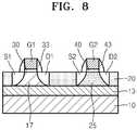
FIG. 8 , according to an example embodiment, a first source electrode S1 and a first drain electrode D1 may be formed at both sides of thefirst layer 17. Alternatively, the first source electrode S1 and the first drain electrode D1 may be formed at a top portion of thefirst layer 17 while being spaced apart from each other. A second source electrode S2 and a second drain electrode D2 may be formed at both sides of thesecond layer 25. Alternatively, the second source electrode S2 and the second drain electrode D2 may be formed at a top portion of thesecond layer 25 while being spaced apart from each other. For example, the first and second source electrodes S1 and S2 and the first and second drain electrodes D1 and D2 may be formed by implantation. However, example embodiments are not limited thereto, and the source electrodes and the drain electrodes may be formed by various other methods. The first and second source electrodes S1 and S2 and the first and second drain electrodes D1 and D2 may be formed of a conductive material, for example, a metal or an alloy. For example, the first and second source electrodes S1 and S2 and the first and second drain electrodes D1 and D2 may be formed of a Ti/Au alloy or a Ge/Au/Ni/Au alloy. - According to an example embodiment, a first
gate insulating layer 30 may be formed on thefirst layer 17, and a secondgate insulating layer 40 may be formed on thesecond layer 25. For example, the first and secondgate insulating layers gate insulating layers gate insulating layer 30, and a second gate electrode G2 may be formed on the secondgate insulating layer 40. Afirst spacer 33 may be formed on both sides of the first gate electrode G1. Asecond spacer 43 may be formed on both sides of the second gate electrode G2. The first gate electrode G1, the first source electrode S1, and the first drain electrode D1 may be formed of various metals or conductive oxide materials. Also, the first gate electrode G1, the first source electrode S1, and the first drain electrode D1 may be formed of the same material, or may be formed of different materials. The second gate electrode G2, the second source electrode S2, and the second drain electrode D2 may be formed of various metals or conductive oxide materials. Also, the second gate electrode G2, the second source electrode S2, and the second drain electrode D2 may be formed of the same material, or may be formed of different materials. Since the first and secondgate insulating layers gate insulating layers second layers - Referring to
FIG. 7 , a CMOS device according to an example embodiment includes asubstrate 10, abuffer layer 13 on thesubstrate 10, and afirst layer 17 for an n-type transistor and asecond layer 25 for a p-type transistor that are disposed on the buffer layer while being spaced apart from each other. Also, an insulatinglayer 20 may be provided between thefirst layer 17 and thesecond layer 25. Accordingly, the CMOS device includes both thefirst layer 17 for the n-type transistor and thesecond layer 25 for the p-type transistor, on onesubstrate 10. FIGS. 9 to 15 illustrate a CMOS device manufacturing method according to another example embodiment. Referring toFIG. 9 , abuffer material layer 113 may be formed on asubstrate 110, and amaterial layer 115 for an n-type transistor may be formed on thebuffer material layer 113. Thesubstrate 110 may be a silicon-based substrate. Also, thesubstrate 110 may be doped with a p-type or n-type dopant. For example, thesubstrate 110 may be a silicon substrate, and may be a p-type silicon substrate.- For example, the
material layer 115 for the n-type transistor may be formed of a Group III-V material. For example, thebuffer material layer 113 may be formed of a Group III-V material of the same series as thematerial layer 115 for the n-type transistor. Since thebuffer material layer 113 and thematerial layer 115 for the n-type transistor may be formed of the same materials and may perform the same operations as thebuffer layer 13 and thematerial layer 15 of the n-type transistor described with reference toFIGS. 2 to 8 , detailed descriptions thereof will be omitted herein. - Referring to
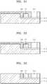
FIG. 10 , according to an example embodiment, thematerial layer 115 for the n-type transistorand thebuffer material layer 113 may be etched to form afirst layer 117 for the n-type transistor, abuffer layer 114 and afirst pattern 118. Thefirst pattern 118 may expose a portion of thesubstrate 110. Referring toFIG. 11 , an insulatinglayer 120 may be formed on thefirst layer 117 for the n-type transistor and an exposed region of thesubstrate 110. The insulatinglayer 120 may be formed of an oxide film, a nitride film, or an oxynitride film. For example, the insulatinglayer 120 may be formed of a silicon oxide (SiO2) film, a silicon nitride (SiNx) film, or a silicon oxynitride (SiOxNy) film. - Referring to
FIG. 12 , according to an example embodiment, the insulatinglayer 120 may be etched to form asecond pattern 123 for selective growth. Thesecond pattern 123 may expose a portion of thesubstrate 110. Referring toFIG. 13 , asecond layer 125 for a p-type transistor may be formed in thesecond pattern 123 by selective growth. The insulatinglayer 120 may be used as a mask in the selective growth process. For example, thesecond layer 125 may be formed of a material including a Group IV material. For example, thesecond layer 125 may be formed of germanium (Ge). Since the surface of thefirst layer 117 is covered with the insulatinglayer 120, thesecond layer 125 may be selectively grown on the exposed region of thesubstrate 110. - Referring to
FIG. 14 , according to an example embodiment, the surfaces of thefirst layer 117 and thesecond layer 125 may be planarized through a planarization process. Accordingly, both thefirst layer 117 for the n-type transistor and thesecond layer 125 for the p-type transistor may be formed on onesubstrate 110. For example, selectively growing thesecond layer 125 formed of a single material may be easier and simpler than selectively growing thefirst layer 117 formed of a Group III-V compound material. - Referring to
FIG. 15 , according to an example embodiment, a first source electrode S11 and a first drain electrode D11 may be formed at both sides of thefirst layer 117. Alternatively, the first source electrode S11 and the first drain electrode D11 may be formed at a top portion of thefirst layer 117 while being spaced apart from each other. A second source electrode S12 and a second drain electrode D12 may be formed at both sides of thesecond layer 125. Afirst spacer 133 may be formed on both sides of a first gate electrode G11. Asecond spacer 143 may be formed on both sides of a second gate electrode G12. Alternatively, the second source electrode S12 and the second drain electrode D12 may be formed at a top portion of thesecond layer 125 while being spaced apart from each other. A firstgate insulating layer 130 may be formed on thefirst layer 117, and the first gate electrode G11 may be formed on the firstgate insulating layer 130. A secondgate insulating layer 140 may be formed on thesecond layer 125, and the second gate electrode G12 may be formed on the secondgate insulating layer 140. - Referring to
FIG. 14 , in a CMOS device according to another example embodiment, abuffer layer 114 may be provided on asubstrate 110, afirst layer 117 for an n-type transistor may be provided on thebuffer layer 114, and asecond layer 125 for a p-type transistor may be provided on thesubstrate 110 while being spaced apart from thefirst layer 117. Also, an insulatinglayer 120 may be provided between thefirst layer 117 and thesecond layer 125. FIGS. 16 to 23 illustrate a CMOS device manufacturing method according to another example embodiment.- Referring to
FIG. 16 , according to an example embodiment, asubstrate 210 is prepared. Referring toFIG. 17 , thesubstrate 210 is etched to form afirst pattern 212. Referring toFIG. 18 , abuffer layer 213 and amaterial layer 215 for an n-type transistor are formed in thefirst pattern 212. Referring toFIG. 19 , thematerial layer 215 for the n-type transistor is etched to form afirst layer 217 for the n-type transistor and asecond pattern 218. Thesecond pattern 218 may be formed to expose thebuffer layer 213 or to expose thesubstrate 210.FIG. 19 illustrates an example in which thebuffer layer 213 is exposed. - Referring to
FIG. 20 , according to an example embodiment, an insulatinglayer 220 is formed on the resulting structure illustrated inFIG. 19 . Referring toFIG. 21 , the insulatinglayer 220 may be etched to form athird pattern 223. Thethird pattern 223 may be a pattern for selective growth. Referring toFIG. 22 , asecond layer 225 for a p-type transistor may be selectively grown in thethird pattern 223. The insulatinglayer 220 may be used as a mask in the selective growth. Referring toFIG. 23 , the surfaces of thesubstrate 210, thefirst layer 217, and thesecond layer 225 may be planarized through a planarization process. Since the components using the same denotations as the components described with reference toFIGS. 2 and8 may be formed of the same materials and may perform the same functions and operations as the corresponding components ofFIGS. 2 and8 , detailed description thereof will be omitted herein. - Through the above process, a plurality of hetero-junction epitaxial structures may be included in one cell of a wafer, according to an example embodiment.
FIG. 24 illustrates an example in which afirst region 310, asecond region 320, and athird region 330 are included in onecell 305 of awafer 300. For example, thefirst region 310 may be asilicon region 310, thesecond region 320 may be a Group III-V compound region, and thethird region 330 may be a Ge region. For example, a photonic device may be provided in thefirst region 310, an n-type transistor may be provided in thesecond region 320, and a p-type transistor may be provided in thethird region 330. For example, the photonic device may be a light emitting diode (LED), a laser diode (LD), or a photodiode (PD). For example, the n-type transistor and the p-type transistor may operate as an electronic device that supports a light-emitting or light-receiving operation of the photonic device. Also, in this way, photonic device integration and hybrid electronic and photonic circuit integration may be possible. - It should be understood that the exemplary embodiments described herein should be considered in a descriptive sense only and not for purposes of limitation. Descriptions of features or example embodiments within each embodiment should typically be considered as available for other similar features or example embodiments.
- While one or more example embodiments have been described with reference to the figures, it will be understood by those of ordinary skill in the art that various changes in form and details may be made therein without departing from the scope of the example embodiments as defined by the following claims.
Claims (12)
- A method of manufacturing a complementary metal oxide semiconductor (CMOS) device comprising a silicon substrate (10), a buffer layer (13) on the silicon substrate, a first layer (17) for an n-type transistor on the buffer layer, a second layer (25) for a p-type transistor disposed on the buffer layer (13) or the silicon substrate (10) while being spaced apart from the first layer (17); and an insulating layer (20) between the first layer (17) and the second layer (25), the method comprising:forming the buffer layer (13) on the silicon substrate (10); forming a material layer (15) for an n-type transistor on the buffer layer (13); etching the material layer (15) for the n-type transistor to form the first layer (17) for the n-type transistor and a first pattern (18), wherein the first layer (17) is formed of a Group III-V material;the methodcharacterized by: forming the insulating layer (20) on the first layer (17) and the first pattern (18); etching the insulating layer (20) to form a second pattern (23) for selective growth; andselectively growing the second layer (25) for a p-type transistor in the second pattern (23) wherein the second layer (25) is formed of a Group IV material.
- The method of claim 1, wherein the forming the first pattern includes etching the material layer to expose a portion of the buffer layer.
- The method of claim 1, wherein the forming the first pattern includes etching the material layer to expose the silicon substrate.
- The method of manufacturing a CMOS device of claim 1, 2 or 3 wherein the buffer layer is formed of a Group III-V material including at least one of indium (In), gallium (Ga), and aluminum (Al), and at least one of arsenic (As), phosphorus (P), and antimony (Sb).
- The method of manufacturing a CMOS device of claim 4, wherein the buffer layer is formed of at least one of InP, InAs, InSb, GaAs, GaP, GaSb, AlP, AlAs, AlSb, InAlAs, InGaP, GaAsP, InGaAsP, and InGaAlAs.
- The method of manufacturing a CMOS device of claim 4 or 5, wherein the buffer layer is doped with an n-type dopant.
- The method of manufacturing a CMOS device of claim 1, 2 or 3 wherein the buffer layer comprises at least one Group IV material.
- The method of manufacturing a CMOS device of claim 7, wherein the buffer layer is formed of at least one of SiGe, GeSn, and germanium (Ge).
- The method of manufacturing a CMOS device of any of claims 1-8, wherein the first layer is formed of at least one of InGaAs, InP, InSb, InGaSb, GaSb, and InAs.
- The method of manufacturing a CMOS device of claim 1, 2 or 3 wherein the second layer is formed of Ge.
- The method of manufacturing a CMOS device of any of claims 1-10, wherein the n-type transistor comprises an n-type metal oxide semiconductor field effect transistor (MOSFET) and/or the p-type transistor comprises a p-type MOSFET.
- The method of manufacturing a CMOS device of any of claims 1-11, wherein the first layer and the second layer are channel layers.
Applications Claiming Priority (1)
| Application Number | Priority Date | Filing Date | Title |
|---|---|---|---|
| KR1020130107502AKR102210325B1 (en) | 2013-09-06 | 2013-09-06 | Complementary metal oxide semiconductor device and method of manufacturing the same |
Publications (3)
| Publication Number | Publication Date |
|---|---|
| EP2846353A2 EP2846353A2 (en) | 2015-03-11 |
| EP2846353A3 EP2846353A3 (en) | 2015-08-12 |
| EP2846353B1true EP2846353B1 (en) | 2017-11-01 |
Family
ID=51453694
Family Applications (1)
| Application Number | Title | Priority Date | Filing Date |
|---|---|---|---|
| EP14183431.7AActiveEP2846353B1 (en) | 2013-09-06 | 2014-09-03 | Method of manufacturing a complementary metal oxide semiconductor device |
Country Status (4)
| Country | Link |
|---|---|
| US (1) | US9425104B2 (en) |
| EP (1) | EP2846353B1 (en) |
| KR (1) | KR102210325B1 (en) |
| CN (1) | CN104425492B (en) |
Families Citing this family (7)
| Publication number | Priority date | Publication date | Assignee | Title |
|---|---|---|---|---|
| WO2015047421A1 (en)* | 2013-09-30 | 2015-04-02 | Hrl Laboratories, Llc | Normally-off iii-nitride transistors with high threshold-voltage and low on-resistance |
| KR102104062B1 (en)* | 2013-10-31 | 2020-04-23 | 삼성전자 주식회사 | Substrate structure, complementary metal oxide semiconductor device and method of manufacturing complementary metal oxide semiconductor |
| US11025029B2 (en) | 2015-07-09 | 2021-06-01 | International Business Machines Corporation | Monolithic III-V nanolaser on silicon with blanket growth |
| US10153300B2 (en)* | 2016-02-05 | 2018-12-11 | Taiwan Semiconductor Manufacturing Company Limited | Semiconductor device including a high-electron-mobility transistor (HEMT) and method for manufacturing the same |
| US11222982B2 (en)* | 2016-09-29 | 2022-01-11 | Intel Corporation | Methods and apparatus to form silicon-based transistors on group III-nitride materials using aspect ratio trapping |
| KR102034175B1 (en) | 2017-05-30 | 2019-10-18 | 한국과학기술연구원 | Semicondutor device with horizontally aligned semiconductor channels and method for manufacturing the same |
| KR102549586B1 (en)* | 2017-08-17 | 2023-07-03 | 한국전자통신연구원 | Fusion semiconductor device and method for fabricating the same |
Family Cites Families (25)
| Publication number | Priority date | Publication date | Assignee | Title |
|---|---|---|---|---|
| US6563143B2 (en)* | 1999-07-29 | 2003-05-13 | Stmicroelectronics, Inc. | CMOS circuit of GaAs/Ge on Si substrate |
| US20040012037A1 (en) | 2002-07-18 | 2004-01-22 | Motorola, Inc. | Hetero-integration of semiconductor materials on silicon |
| US7153753B2 (en)* | 2003-08-05 | 2006-12-26 | Micron Technology, Inc. | Strained Si/SiGe/SOI islands and processes of making same |
| US7138697B2 (en) | 2004-02-24 | 2006-11-21 | International Business Machines Corporation | Structure for and method of fabricating a high-speed CMOS-compatible Ge-on-insulator photodetector |
| JP4177775B2 (en)* | 2004-03-16 | 2008-11-05 | 株式会社東芝 | Semiconductor substrate, manufacturing method thereof, and semiconductor device |
| US7422956B2 (en) | 2004-12-08 | 2008-09-09 | Advanced Micro Devices, Inc. | Semiconductor device and method of making semiconductor device comprising multiple stacked hybrid orientation layers |
| US7569873B2 (en) | 2005-10-28 | 2009-08-04 | Dsm Solutions, Inc. | Integrated circuit using complementary junction field effect transistor and MOS transistor in silicon and silicon alloys |
| KR100843229B1 (en) | 2007-01-11 | 2008-07-02 | 삼성전자주식회사 | Flash memory device comprising a charge trap film of a hybrid structure and a manufacturing method thereof |
| US7510940B2 (en) | 2007-02-16 | 2009-03-31 | Taiwan Semiconductor Manufacturing Company, Ltd. | Method for fabricating dual-gate semiconductor device |
| US9006707B2 (en)* | 2007-02-28 | 2015-04-14 | Intel Corporation | Forming arsenide-based complementary logic on a single substrate |
| KR20090038653A (en) | 2007-10-16 | 2009-04-21 | 삼성전자주식회사 | CMOS device and method of manufacturing the same |
| KR101020841B1 (en) | 2008-03-31 | 2011-03-09 | 고려대학교 산학협력단 | CMOS device and its manufacturing method |
| WO2010010944A1 (en) | 2008-07-25 | 2010-01-28 | 国立大学法人東北大学 | Complementary logical gate device |
| KR20100078548A (en) | 2008-12-30 | 2010-07-08 | 주식회사 동부하이텍 | Method of fabricating a cmos type semiconductor device having dual gates |
| US8530938B2 (en)* | 2009-12-10 | 2013-09-10 | International Rectifier Corporation | Monolithic integrated composite group III-V and group IV semiconductor device and method for fabricating same |
| US8212294B2 (en) | 2010-01-28 | 2012-07-03 | Raytheon Company | Structure having silicon CMOS transistors with column III-V transistors on a common substrate |
| CN102790054B (en)* | 2011-05-16 | 2015-09-16 | 中国科学院上海微系统与信息技术研究所 | Germanium and III-V mix coplanar semiconductor structure and preparation method thereof |
| CN102790084B (en)* | 2011-05-16 | 2016-03-16 | 中国科学院上海微系统与信息技术研究所 | Germanium and III-V mix coplanar soi semiconductor structure and preparation method thereof |
| CN102842595B (en)* | 2011-06-20 | 2015-12-02 | 中国科学院微电子研究所 | Semiconductor device and method for manufacturing the same |
| US9165835B2 (en) | 2011-08-30 | 2015-10-20 | Taiwan Semiconductor Manufacturing Co., Ltd. | Method and structure for advanced semiconductor channel substrate materials |
| US20130137238A1 (en) | 2011-11-30 | 2013-05-30 | Taiwan Semiconductor Manufacturing Company, Ltd. | Method for forming high mobility channels in iii-v family channel devices |
| US8471342B1 (en)* | 2011-12-09 | 2013-06-25 | GlobalFoundries, Inc. | Integrated circuits formed on strained substrates and including relaxed buffer layers and methods for the manufacture thereof |
| KR101167530B1 (en) | 2012-01-05 | 2012-07-20 | 주식회사 시지트로닉스 | Super heterojunction semiconductor device structure and its fabrication method |
| CN103258796B (en)* | 2013-05-14 | 2015-01-28 | 中国科学院半导体研究所 | Method for manufacturing silicon-substrate high-migration-rate channel CMOS |
| CN103390591B (en) | 2013-07-22 | 2015-11-25 | 中国科学院半导体研究所 | The CMOS preparation method of silica-based high mobility III-V/Ge raceway groove |
- 2013
- 2013-09-06KRKR1020130107502Apatent/KR102210325B1/enactiveActive
- 2014
- 2014-04-23USUS14/259,569patent/US9425104B2/enactiveActive
- 2014-09-02CNCN201410442976.4Apatent/CN104425492B/enactiveActive
- 2014-09-03EPEP14183431.7Apatent/EP2846353B1/enactiveActive
Non-Patent Citations (1)
| Title |
|---|
| None* |
Also Published As
| Publication number | Publication date |
|---|---|
| KR102210325B1 (en) | 2021-02-01 |
| EP2846353A3 (en) | 2015-08-12 |
| KR20150028626A (en) | 2015-03-16 |
| CN104425492A (en) | 2015-03-18 |
| CN104425492B (en) | 2019-03-22 |
| EP2846353A2 (en) | 2015-03-11 |
| US20150069517A1 (en) | 2015-03-12 |
| US9425104B2 (en) | 2016-08-23 |
Similar Documents
| Publication | Publication Date | Title |
|---|---|---|
| EP2846353B1 (en) | Method of manufacturing a complementary metal oxide semiconductor device | |
| KR102551812B1 (en) | Electronic power devices integrated with an engineered substrat | |
| KR102681469B1 (en) | Systems and methods for integrated devices on fabricated substrates | |
| US9412911B2 (en) | Optical tuning of light emitting semiconductor junctions | |
| US9312377B2 (en) | Semiconductor devices and methods of manufacturing the same | |
| US8866154B2 (en) | Lattice mismatched heterojunction structures and devices made therefrom | |
| US9105496B2 (en) | Complementary metal oxide semiconductor device, optical apparatus including the same, and method of manufacturing the same | |
| EP2787525A1 (en) | Substrate structures and semiconductor devices employing the same | |
| JP6525554B2 (en) | CMOS device including substrate structure | |
| US20110315953A1 (en) | Method of forming compound semiconductor | |
| US9595616B1 (en) | Vertical III-nitride thin-film power diode | |
| KR102034175B1 (en) | Semicondutor device with horizontally aligned semiconductor channels and method for manufacturing the same | |
| US8536028B1 (en) | Self alignment and assembly fabrication method for stacking multiple material layers | |
| JP2014090122A (en) | Composite substrate manufacturing method | |
| Liu et al. | n+ Si/pGe Heterojunctions Fabricated by Narrow Membrane Bonding |
Legal Events
| Date | Code | Title | Description |
|---|---|---|---|
| 17P | Request for examination filed | Effective date:20140903 | |
| AK | Designated contracting states | Kind code of ref document:A2 Designated state(s):AL AT BE BG CH CY CZ DE DK EE ES FI FR GB GR HR HU IE IS IT LI LT LU LV MC MK MT NL NO PL PT RO RS SE SI SK SM TR | |
| AX | Request for extension of the european patent | Extension state:BA ME | |
| PUAI | Public reference made under article 153(3) epc to a published international application that has entered the european phase | Free format text:ORIGINAL CODE: 0009012 | |
| PUAL | Search report despatched | Free format text:ORIGINAL CODE: 0009013 | |
| AK | Designated contracting states | Kind code of ref document:A3 Designated state(s):AL AT BE BG CH CY CZ DE DK EE ES FI FR GB GR HR HU IE IS IT LI LT LU LV MC MK MT NL NO PL PT RO RS SE SI SK SM TR | |
| AX | Request for extension of the european patent | Extension state:BA ME | |
| RIC1 | Information provided on ipc code assigned before grant | Ipc:H01L 27/06 20060101ALI20150706BHEP Ipc:H01L 27/092 20060101ALI20150706BHEP Ipc:H01L 21/8238 20060101ALI20150706BHEP Ipc:H01L 21/8252 20060101AFI20150706BHEP Ipc:H01L 21/8258 20060101ALI20150706BHEP | |
| R17P | Request for examination filed (corrected) | Effective date:20160212 | |
| RBV | Designated contracting states (corrected) | Designated state(s):AL AT BE BG CH CY CZ DE DK EE ES FI FR GB GR HR HU IE IS IT LI LT LU LV MC MK MT NL NO PL PT RO RS SE SI SK SM TR | |
| GRAP | Despatch of communication of intention to grant a patent | Free format text:ORIGINAL CODE: EPIDOSNIGR1 | |
| INTG | Intention to grant announced | Effective date:20170601 | |
| GRAS | Grant fee paid | Free format text:ORIGINAL CODE: EPIDOSNIGR3 | |
| GRAA | (expected) grant | Free format text:ORIGINAL CODE: 0009210 | |
| AK | Designated contracting states | Kind code of ref document:B1 Designated state(s):AL AT BE BG CH CY CZ DE DK EE ES FI FR GB GR HR HU IE IS IT LI LT LU LV MC MK MT NL NO PL PT RO RS SE SI SK SM TR | |
| REG | Reference to a national code | Ref country code:GB Ref legal event code:FG4D | |
| REG | Reference to a national code | Ref country code:CH Ref legal event code:EP Ref country code:AT Ref legal event code:REF Ref document number:942823 Country of ref document:AT Kind code of ref document:T Effective date:20171115 | |
| REG | Reference to a national code | Ref country code:IE Ref legal event code:FG4D | |
| REG | Reference to a national code | Ref country code:DE Ref legal event code:R096 Ref document number:602014016493 Country of ref document:DE | |
| REG | Reference to a national code | Ref country code:NL Ref legal event code:MP Effective date:20171101 | |
| REG | Reference to a national code | Ref country code:LT Ref legal event code:MG4D | |
| REG | Reference to a national code | Ref country code:AT Ref legal event code:MK05 Ref document number:942823 Country of ref document:AT Kind code of ref document:T Effective date:20171101 | |
| PG25 | Lapsed in a contracting state [announced via postgrant information from national office to epo] | Ref country code:NL Free format text:LAPSE BECAUSE OF FAILURE TO SUBMIT A TRANSLATION OF THE DESCRIPTION OR TO PAY THE FEE WITHIN THE PRESCRIBED TIME-LIMIT Effective date:20171101 Ref country code:FI Free format text:LAPSE BECAUSE OF FAILURE TO SUBMIT A TRANSLATION OF THE DESCRIPTION OR TO PAY THE FEE WITHIN THE PRESCRIBED TIME-LIMIT Effective date:20171101 Ref country code:LT Free format text:LAPSE BECAUSE OF FAILURE TO SUBMIT A TRANSLATION OF THE DESCRIPTION OR TO PAY THE FEE WITHIN THE PRESCRIBED TIME-LIMIT Effective date:20171101 Ref country code:SE Free format text:LAPSE BECAUSE OF FAILURE TO SUBMIT A TRANSLATION OF THE DESCRIPTION OR TO PAY THE FEE WITHIN THE PRESCRIBED TIME-LIMIT Effective date:20171101 Ref country code:NO Free format text:LAPSE BECAUSE OF FAILURE TO SUBMIT A TRANSLATION OF THE DESCRIPTION OR TO PAY THE FEE WITHIN THE PRESCRIBED TIME-LIMIT Effective date:20180201 Ref country code:ES Free format text:LAPSE BECAUSE OF FAILURE TO SUBMIT A TRANSLATION OF THE DESCRIPTION OR TO PAY THE FEE WITHIN THE PRESCRIBED TIME-LIMIT Effective date:20171101 | |
| PG25 | Lapsed in a contracting state [announced via postgrant information from national office to epo] | Ref country code:AT Free format text:LAPSE BECAUSE OF FAILURE TO SUBMIT A TRANSLATION OF THE DESCRIPTION OR TO PAY THE FEE WITHIN THE PRESCRIBED TIME-LIMIT Effective date:20171101 Ref country code:HR Free format text:LAPSE BECAUSE OF FAILURE TO SUBMIT A TRANSLATION OF THE DESCRIPTION OR TO PAY THE FEE WITHIN THE PRESCRIBED TIME-LIMIT Effective date:20171101 Ref country code:BG Free format text:LAPSE BECAUSE OF FAILURE TO SUBMIT A TRANSLATION OF THE DESCRIPTION OR TO PAY THE FEE WITHIN THE PRESCRIBED TIME-LIMIT Effective date:20180201 Ref country code:LV Free format text:LAPSE BECAUSE OF FAILURE TO SUBMIT A TRANSLATION OF THE DESCRIPTION OR TO PAY THE FEE WITHIN THE PRESCRIBED TIME-LIMIT Effective date:20171101 Ref country code:RS Free format text:LAPSE BECAUSE OF FAILURE TO SUBMIT A TRANSLATION OF THE DESCRIPTION OR TO PAY THE FEE WITHIN THE PRESCRIBED TIME-LIMIT Effective date:20171101 Ref country code:GR Free format text:LAPSE BECAUSE OF FAILURE TO SUBMIT A TRANSLATION OF THE DESCRIPTION OR TO PAY THE FEE WITHIN THE PRESCRIBED TIME-LIMIT Effective date:20180202 Ref country code:IS Free format text:LAPSE BECAUSE OF FAILURE TO SUBMIT A TRANSLATION OF THE DESCRIPTION OR TO PAY THE FEE WITHIN THE PRESCRIBED TIME-LIMIT Effective date:20180301 | |
| PG25 | Lapsed in a contracting state [announced via postgrant information from national office to epo] | Ref country code:SK Free format text:LAPSE BECAUSE OF FAILURE TO SUBMIT A TRANSLATION OF THE DESCRIPTION OR TO PAY THE FEE WITHIN THE PRESCRIBED TIME-LIMIT Effective date:20171101 Ref country code:DK Free format text:LAPSE BECAUSE OF FAILURE TO SUBMIT A TRANSLATION OF THE DESCRIPTION OR TO PAY THE FEE WITHIN THE PRESCRIBED TIME-LIMIT Effective date:20171101 Ref country code:CY Free format text:LAPSE BECAUSE OF FAILURE TO SUBMIT A TRANSLATION OF THE DESCRIPTION OR TO PAY THE FEE WITHIN THE PRESCRIBED TIME-LIMIT Effective date:20171101 Ref country code:EE Free format text:LAPSE BECAUSE OF FAILURE TO SUBMIT A TRANSLATION OF THE DESCRIPTION OR TO PAY THE FEE WITHIN THE PRESCRIBED TIME-LIMIT Effective date:20171101 Ref country code:CZ Free format text:LAPSE BECAUSE OF FAILURE TO SUBMIT A TRANSLATION OF THE DESCRIPTION OR TO PAY THE FEE WITHIN THE PRESCRIBED TIME-LIMIT Effective date:20171101 | |
| REG | Reference to a national code | Ref country code:DE Ref legal event code:R097 Ref document number:602014016493 Country of ref document:DE | |
| PG25 | Lapsed in a contracting state [announced via postgrant information from national office to epo] | Ref country code:RO Free format text:LAPSE BECAUSE OF FAILURE TO SUBMIT A TRANSLATION OF THE DESCRIPTION OR TO PAY THE FEE WITHIN THE PRESCRIBED TIME-LIMIT Effective date:20171101 Ref country code:IT Free format text:LAPSE BECAUSE OF FAILURE TO SUBMIT A TRANSLATION OF THE DESCRIPTION OR TO PAY THE FEE WITHIN THE PRESCRIBED TIME-LIMIT Effective date:20171101 Ref country code:SM Free format text:LAPSE BECAUSE OF FAILURE TO SUBMIT A TRANSLATION OF THE DESCRIPTION OR TO PAY THE FEE WITHIN THE PRESCRIBED TIME-LIMIT Effective date:20171101 Ref country code:PL Free format text:LAPSE BECAUSE OF FAILURE TO SUBMIT A TRANSLATION OF THE DESCRIPTION OR TO PAY THE FEE WITHIN THE PRESCRIBED TIME-LIMIT Effective date:20171101 | |
| PLBE | No opposition filed within time limit | Free format text:ORIGINAL CODE: 0009261 | |
| STAA | Information on the status of an ep patent application or granted ep patent | Free format text:STATUS: NO OPPOSITION FILED WITHIN TIME LIMIT | |
| 26N | No opposition filed | Effective date:20180802 | |
| PG25 | Lapsed in a contracting state [announced via postgrant information from national office to epo] | Ref country code:SI Free format text:LAPSE BECAUSE OF FAILURE TO SUBMIT A TRANSLATION OF THE DESCRIPTION OR TO PAY THE FEE WITHIN THE PRESCRIBED TIME-LIMIT Effective date:20171101 | |
| PG25 | Lapsed in a contracting state [announced via postgrant information from national office to epo] | Ref country code:MC Free format text:LAPSE BECAUSE OF FAILURE TO SUBMIT A TRANSLATION OF THE DESCRIPTION OR TO PAY THE FEE WITHIN THE PRESCRIBED TIME-LIMIT Effective date:20171101 | |
| REG | Reference to a national code | Ref country code:CH Ref legal event code:PL | |
| GBPC | Gb: european patent ceased through non-payment of renewal fee | Effective date:20180903 | |
| REG | Reference to a national code | Ref country code:BE Ref legal event code:MM Effective date:20180930 | |
| REG | Reference to a national code | Ref country code:IE Ref legal event code:MM4A | |
| PG25 | Lapsed in a contracting state [announced via postgrant information from national office to epo] | Ref country code:LU Free format text:LAPSE BECAUSE OF NON-PAYMENT OF DUE FEES Effective date:20180903 | |
| PG25 | Lapsed in a contracting state [announced via postgrant information from national office to epo] | Ref country code:IE Free format text:LAPSE BECAUSE OF NON-PAYMENT OF DUE FEES Effective date:20180903 | |
| PG25 | Lapsed in a contracting state [announced via postgrant information from national office to epo] | Ref country code:BE Free format text:LAPSE BECAUSE OF NON-PAYMENT OF DUE FEES Effective date:20180930 Ref country code:CH Free format text:LAPSE BECAUSE OF NON-PAYMENT OF DUE FEES Effective date:20180930 Ref country code:LI Free format text:LAPSE BECAUSE OF NON-PAYMENT OF DUE FEES Effective date:20180930 Ref country code:FR Free format text:LAPSE BECAUSE OF NON-PAYMENT OF DUE FEES Effective date:20180930 | |
| PG25 | Lapsed in a contracting state [announced via postgrant information from national office to epo] | Ref country code:GB Free format text:LAPSE BECAUSE OF NON-PAYMENT OF DUE FEES Effective date:20180903 | |
| PG25 | Lapsed in a contracting state [announced via postgrant information from national office to epo] | Ref country code:MT Free format text:LAPSE BECAUSE OF NON-PAYMENT OF DUE FEES Effective date:20180903 | |
| PG25 | Lapsed in a contracting state [announced via postgrant information from national office to epo] | Ref country code:TR Free format text:LAPSE BECAUSE OF FAILURE TO SUBMIT A TRANSLATION OF THE DESCRIPTION OR TO PAY THE FEE WITHIN THE PRESCRIBED TIME-LIMIT Effective date:20171101 | |
| PG25 | Lapsed in a contracting state [announced via postgrant information from national office to epo] | Ref country code:HU Free format text:LAPSE BECAUSE OF FAILURE TO SUBMIT A TRANSLATION OF THE DESCRIPTION OR TO PAY THE FEE WITHIN THE PRESCRIBED TIME-LIMIT; INVALID AB INITIO Effective date:20140903 Ref country code:PT Free format text:LAPSE BECAUSE OF FAILURE TO SUBMIT A TRANSLATION OF THE DESCRIPTION OR TO PAY THE FEE WITHIN THE PRESCRIBED TIME-LIMIT Effective date:20171101 | |
| PG25 | Lapsed in a contracting state [announced via postgrant information from national office to epo] | Ref country code:MK Free format text:LAPSE BECAUSE OF NON-PAYMENT OF DUE FEES Effective date:20171101 | |
| PG25 | Lapsed in a contracting state [announced via postgrant information from national office to epo] | Ref country code:AL Free format text:LAPSE BECAUSE OF FAILURE TO SUBMIT A TRANSLATION OF THE DESCRIPTION OR TO PAY THE FEE WITHIN THE PRESCRIBED TIME-LIMIT Effective date:20171101 | |
| P01 | Opt-out of the competence of the unified patent court (upc) registered | Effective date:20230520 | |
| PGFP | Annual fee paid to national office [announced via postgrant information from national office to epo] | Ref country code:DE Payment date:20240723 Year of fee payment:11 | |
| REG | Reference to a national code | Ref country code:DE Ref legal event code:R079 Ref document number:602014016493 Country of ref document:DE Free format text:PREVIOUS MAIN CLASS: H01L0021825200 Ipc:H10D0084050000 |