EP2843853B1 - Optical module and preparation method therefor - Google Patents
Optical module and preparation method thereforDownload PDFInfo
- Publication number
- EP2843853B1 EP2843853B1EP13883756.2AEP13883756AEP2843853B1EP 2843853 B1EP2843853 B1EP 2843853B1EP 13883756 AEP13883756 AEP 13883756AEP 2843853 B1EP2843853 B1EP 2843853B1
- Authority
- EP
- European Patent Office
- Prior art keywords
- electro
- optical
- absorption modulator
- laser
- optical amplifier
- Prior art date
- Legal status (The legal status is an assumption and is not a legal conclusion. Google has not performed a legal analysis and makes no representation as to the accuracy of the status listed.)
- Active
Links
- 230000003287optical effectEffects0.000titleclaimsdescription329
- 238000002360preparation methodMethods0.000title1
- 239000004065semiconductorSubstances0.000claimsdescription131
- 238000010521absorption reactionMethods0.000claimsdescription117
- 239000000758substrateSubstances0.000claimsdescription64
- 239000000463materialSubstances0.000claimsdescription55
- 238000000034methodMethods0.000claimsdescription34
- 238000005530etchingMethods0.000claimsdescription20
- VYPSYNLAJGMNEJ-UHFFFAOYSA-NSilicium dioxideChemical compoundO=[Si]=OVYPSYNLAJGMNEJ-UHFFFAOYSA-N0.000description12
- 230000005540biological transmissionEffects0.000description10
- 239000013307optical fiberSubstances0.000description8
- 238000010586diagramMethods0.000description7
- 238000011161developmentMethods0.000description6
- 230000008569processEffects0.000description6
- 230000035945sensitivityEffects0.000description6
- 235000012239silicon dioxideNutrition0.000description6
- 239000000377silicon dioxideSubstances0.000description6
- 230000008878couplingEffects0.000description5
- 238000010168coupling processMethods0.000description5
- 238000005859coupling reactionMethods0.000description5
- 230000006870functionEffects0.000description5
- 230000006855networkingEffects0.000description5
- 238000004891communicationMethods0.000description3
- 230000017525heat dissipationEffects0.000description3
- 238000004519manufacturing processMethods0.000description3
- 238000003860storageMethods0.000description3
- 238000009826distributionMethods0.000description2
- 230000000694effectsEffects0.000description2
- 229910001218Gallium arsenideInorganic materials0.000description1
- 238000013461designMethods0.000description1
- 238000005516engineering processMethods0.000description1
- 238000012545processingMethods0.000description1
Images


Classifications
- H—ELECTRICITY
- H01—ELECTRIC ELEMENTS
- H01S—DEVICES USING THE PROCESS OF LIGHT AMPLIFICATION BY STIMULATED EMISSION OF RADIATION [LASER] TO AMPLIFY OR GENERATE LIGHT; DEVICES USING STIMULATED EMISSION OF ELECTROMAGNETIC RADIATION IN WAVE RANGES OTHER THAN OPTICAL
- H01S5/00—Semiconductor lasers
- H01S5/02—Structural details or components not essential to laser action
- H01S5/026—Monolithically integrated components, e.g. waveguides, monitoring photo-detectors, drivers
- H01S5/0265—Intensity modulators
- H—ELECTRICITY
- H04—ELECTRIC COMMUNICATION TECHNIQUE
- H04B—TRANSMISSION
- H04B10/00—Transmission systems employing electromagnetic waves other than radio-waves, e.g. infrared, visible or ultraviolet light, or employing corpuscular radiation, e.g. quantum communication
- H04B10/27—Arrangements for networking
- H—ELECTRICITY
- H04—ELECTRIC COMMUNICATION TECHNIQUE
- H04B—TRANSMISSION
- H04B10/00—Transmission systems employing electromagnetic waves other than radio-waves, e.g. infrared, visible or ultraviolet light, or employing corpuscular radiation, e.g. quantum communication
- H04B10/50—Transmitters
- H04B10/501—Structural aspects
- H04B10/503—Laser transmitters
- H04B10/505—Laser transmitters using external modulation
- H—ELECTRICITY
- H04—ELECTRIC COMMUNICATION TECHNIQUE
- H04B—TRANSMISSION
- H04B10/00—Transmission systems employing electromagnetic waves other than radio-waves, e.g. infrared, visible or ultraviolet light, or employing corpuscular radiation, e.g. quantum communication
- H04B10/50—Transmitters
- H04B10/564—Power control
- H—ELECTRICITY
- H01—ELECTRIC ELEMENTS
- H01S—DEVICES USING THE PROCESS OF LIGHT AMPLIFICATION BY STIMULATED EMISSION OF RADIATION [LASER] TO AMPLIFY OR GENERATE LIGHT; DEVICES USING STIMULATED EMISSION OF ELECTROMAGNETIC RADIATION IN WAVE RANGES OTHER THAN OPTICAL
- H01S5/00—Semiconductor lasers
- H01S5/005—Optical components external to the laser cavity, specially adapted therefor, e.g. for homogenisation or merging of the beams or for manipulating laser pulses, e.g. pulse shaping
- H01S5/0085—Optical components external to the laser cavity, specially adapted therefor, e.g. for homogenisation or merging of the beams or for manipulating laser pulses, e.g. pulse shaping for modulating the output, i.e. the laser beam is modulated outside the laser cavity
- H—ELECTRICITY
- H01—ELECTRIC ELEMENTS
- H01S—DEVICES USING THE PROCESS OF LIGHT AMPLIFICATION BY STIMULATED EMISSION OF RADIATION [LASER] TO AMPLIFY OR GENERATE LIGHT; DEVICES USING STIMULATED EMISSION OF ELECTROMAGNETIC RADIATION IN WAVE RANGES OTHER THAN OPTICAL
- H01S5/00—Semiconductor lasers
- H01S5/02—Structural details or components not essential to laser action
- H01S5/022—Mountings; Housings
- H01S5/0225—Out-coupling of light
- H01S5/02251—Out-coupling of light using optical fibres
- H—ELECTRICITY
- H01—ELECTRIC ELEMENTS
- H01S—DEVICES USING THE PROCESS OF LIGHT AMPLIFICATION BY STIMULATED EMISSION OF RADIATION [LASER] TO AMPLIFY OR GENERATE LIGHT; DEVICES USING STIMULATED EMISSION OF ELECTROMAGNETIC RADIATION IN WAVE RANGES OTHER THAN OPTICAL
- H01S5/00—Semiconductor lasers
- H01S5/50—Amplifier structures not provided for in groups H01S5/02 - H01S5/30
Definitions
- the present inventionrelates to the field of optical communication technologies, and in particular, to an optical module and a fabrication method thereof.
- a passive optical networkdoes not include an electronic component or electrical power supply but includes an optical line terminal (Optical Line Terminal, OLT) that is installed at a central control station and a batch of matching optical network units (Optical Network Unit, ONU) that are installed at a user site.
- An optical distribution network(Optical Distribution Network, ODN) between the OLT and the ONUs includes optical fibers, a passive optical splitter or a coupler, and the like.
- the ODNis formed by passive components such as an optical splitter (Splitter), without requiring an expensive active electronic device.
- An access network of a next generationdevelops towards high bandwidth of 10G.
- the PON networkis subject to a 1:64 or even 1:128 application.
- an optical module on the OLT sidehas low output optical power. Therefore, the ONU side needs to use a high-sensitivity component.
- a 10G optical module on the OLT sideuses an electro-absorption modulated laser (Electro-absorption Modulated Laser, EML) to transmit an optical signal, and its specification of the output optical power is 2-6 dBm.
- EMLElectro-absorption Modulated Laser
- EP 1 840 607 A1(FUJITSU LTD [JP]) 3 October 2007) discloses a method of fabricating an optical module comprising laser, SOA, and EOM, which comprises the steps of growing and etching an epitaxial material.
- Embodiments of the present inventionprovide methods for fabricating an optical module, which can increase output optical power of the optical module.
- a first aspectprovides a method for fabricating an optical module, including:
- the methodfurther includes:
- a second aspectprovides a method for fabricating an optical module, including:
- the methodfurther includes:
- an electro-absorption modulated laseris integrated with a semiconductor optical amplifier, and an optical signal output by the laser is amplified, thereby increasing optical power output by an optical module and having a lower requirement on sensitivity of an optical component on an ONU side.
- a low-sensitivity PIN chipinstead of an APD chip may be used on the ONU side.
- use of a low-sensitivity componentsignificantly reduces networking costs and promotes development of an access network towards high bandwidth.
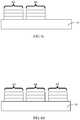
- FIG. 1is a schematic structural diagram of an optical module according to an embodiment of the present invention.
- the optical modulemay include a substrate 10, a laser 101, an electro-absorption modulator 102, and a semiconductor optical amplifier 103 that grow on the substrate 10, and an optical component 11.
- the electro-absorption modulator 102is located between the laser 101 and the semiconductor optical amplifier 103, and these three components may be arranged in a line on the substrate 10.
- a combination of the laser 101 and the electro-absorption modulator 102is an EML.
- the laser 101is configured to output an optical signal after power-on; the electro-absorption modulator 102 is configured to perform signal modulation on the optical signal output by the laser 101; the semiconductor optical amplifier 103 is configured to amplify the optical signal modulated by the electro-absorption modulator 102; the optical component 11 is configured to perform deflection and convergence for the optical signal amplified by the semiconductor optical amplifier 103 and output the optical signal.
- an electro-absorption modulated laseris integrated with a semiconductor optical amplifier, and an optical signal output by the laser is amplified, thereby increasing optical power output by an optical module and having a lower requirement on sensitivity of an optical component on an ONU side.
- a low-sensitivity PIN chipinstead of an APD chip may be used on the ONU side.
- use of a low-sensitivity componentsignificantly reduces networking costs and promotes development of an access network towards high bandwidth.
- the optical modulemay further include a semiconductor refrigerator 21, where the semiconductor refrigerator 21 abuts against the substrate 10 and is located on one side of the substrate that is opposite to the side of the substrate where the laser 101, the electro-absorption modulator 102, and the semiconductor optical amplifier 103 are located.
- luminescent materials of the laser and the electro-absorption modulator and a material of the semiconductor optical amplifiermay be InP doped with GaAs. Therefore, an InP material may be selected as the substrate to grow epitaxial layers of both the EML (the laser and the electro-absorption modulator) and the semiconductor optical amplifier.
- An internal structure of the EML and an internal structure of the semiconductor optical amplifierare similar to those in the prior art, which are not further described herein.
- the optical component in the foregoing embodimentsmay be similar to that in the prior art.
- the optical componentincludes an optical lens 221a/221b, an optical isolator 222, and an optical fiber 223.
- the optical lens 221ais mainly configured to converge optical signals output by the semiconductor optical amplifier 103, so as to improve coupling efficiency of the optical signals.
- the optical isolator 222is configured to enable an optical signal that passes through the optical lens 221a to deflect by 90 degrees, so as to prevent light reflected back to the laser from forming a resonance effect and prevent an impact on performance.
- the optical lens 221bis mainly configured to couple an optical signal that passes through the optical isolator 222 into the optical fiber 223.
- the optical fiber 223outputs the optical signal that passes through the optical isolator 222 out of the optical module.
- An embodiment of the present inventionfurther provides a passive optical network, including an optical line terminal and an optical network unit; where: the optical line terminal is connected to the optical network unit by using an optical transmission channel; the optical line terminal is configured to send Ethernet data to the optical network unit over the optical transmission channel, and receive, over the optical transmission channel, Ethernet data uploaded by the optical network unit; the optical network unit is configured to receive, over the optical transmission channel, the Ethernet data sent by the optical line terminal, and upload the Ethernet data to the optical line terminal over the optical transmission channel; the optical line terminal includes the optical module shown in FIG. 1 or FIG. 2 .
- FIG. 3is a schematic structural diagram of another optical module according to an embodiment of the present invention.
- the optical module in this embodimentdiffers from the optical module in the foregoing embodiment in that: an arrangement sequence of a laser, an electro-absorption modulator, and a semiconductor optical amplifier that grow on a substrate is different from that in the foregoing embodiment; in this embodiment, the semiconductor optical amplifier is located between the laser and the electro-absorption modulator.
- the optical modulemay include an optical component 31, a substrate 32, and a laser 321, a semiconductor optical amplifier 322, and an electro-absorption modulator 323 that grow on the substrate 32, where the semiconductor optical amplifier 322 is located between the laser 321 and the electro-absorption modulator 323 and these three components may be arranged in a line.
- the laser 321is configured to output an optical signal after power-on.
- the semiconductor optical amplifier 322is configured to amplify the optical signal output by the laser 321.
- the electro-absorption modulator 323is configured to perform signal modulation on the optical signal amplified by the semiconductor optical amplifier 322.
- the optical component 31is configured to perform deflection and convergence for the optical signal modulated by the electro-absorption modulator 323 and output the optical signal out of the optical module.
- an electro-absorption modulated laseris integrated with a semiconductor optical amplifier, and an optical signal output by the laser is amplified, thereby increasing optical power output by an optical module and having a lower requirement on sensitivity of an optical component on an ONU side.
- a low-sensitivity PIN chipinstead of an APD chip may be used on the ONU side.
- use of a low-sensitivity componentsignificantly reduces networking costs and promotes development of an access network towards high bandwidth.
- the optical modulemay further include a semiconductor refrigerator 41, where the semiconductor refrigerator 41 abuts against the substrate 32 and is located on one side of substrate 32 that is opposite to the side of the substrate 32 where the laser 321, the semiconductor optical amplifier 322, and the electro-absorption modulator 232 are located.
- the semiconductor refrigerator 41 arranged on the substratemay facilitate heat dissipation of a component that outputs light by using high power.
- an InP materialmay also be selected as the substrate to grow epitaxial layers of both the laser, the semiconductor optical amplifier, and the electro-absorption modulator.
- Internal structures of the laser and the electro-absorption modulator and an internal structure of the semiconductor optical amplifierare similar to those in the prior art, which are not further described herein.
- the optical componentmay be similar to the optical component in the foregoing embodiments.
- the optical componentincludes an optical lens 421a/421b, an optical isolator 422, and an optical fiber 423.
- the optical lens 421ais configured to converge optical signals output by the electro-absorption modulator 323, so as to improve coupling efficiency of the optical signals.
- the optical isolator 422is configured to enable an optical signal that passes through the optical lens 421a to deflect by 90 degrees, so as to prevent light reflected back to the laser from forming a resonance effect and prevent an impact on performance.
- the optical lens 421bis configured to couple an optical signal that passes through the optical isolator 422 into the optical fiber 423.
- the optical fiber 423outputs the optical signal that passes through the optical isolator 422 out of the optical module.
- An embodiment of the present inventionfurther provides a passive optical network, including an optical line terminal and an optical network unit; where: the optical line terminal is connected to the optical network unit by using an optical transmission channel; the optical line terminal is configured to send Ethernet data to the optical network unit over the optical transmission channel, and receive, over the optical transmission channel, Ethernet data uploaded by the optical network unit; the optical network unit is configured to receive, over the optical transmission channel, the Ethernet data sent by the optical line terminal, and upload the Ethernet data to the optical line terminal over the optical transmission channel; the optical line terminal includes the optical module as shown in FIG. 3 or FIG. 4 .
- optical module embodiments of the present inventiondescribes the optical module embodiments of the present invention.
- the followingdescribes a method for fabricating the foregoing optical modules.
- FIG. 5is a flowchart of a method for fabricating an optical module according to an embodiment of the present invention.
- This embodiment of the present inventionis used for fabricating the optical module shown in FIG. 1 or FIG. 2 .
- the methodmay include:
- the substrate 61may be made of InP, and then an epitaxial material 62 of the laser is grown on the substrate 61.
- the epitaxial material of the laser and a growing processare similar to those in the prior art, which are not further described herein.
- Step 502Etch the epitaxial material of the laser to acquire the laser and an electro-absorption modulator window.
- the epitaxial material 62 of the laseris grown, the epitaxial material is etched to acquire a laser 63, and further the electro-absorption modulator window is acquired by etching, as shown in FIG. 6b .
- Step 503Grow an epitaxial material of an electro-absorption modulator in the electro-absorption modulator window on the substrate.
- the epitaxial material of the electro-absorption modulatoris grown in electro-absorption modulator window, which is acquired by etching, on the substrate 61, where the epitaxial material of the electro-absorption modulator and a grown process thereof are similar to those in the prior art.
- a protection layerfor example, a silicon dioxide layer, may be firstly deposited to cover the laser, and then the epitaxial material of the electro-absorption modulator is deposited in the electro-absorption modulator window on the substrate.
- Step 504Etch the epitaxial material of the electro-absorption modulator to acquire the electro-absorption modulator and a semiconductor optical amplifier window, where the electro-absorption modulator is located between the laser and the semiconductor optical amplifier window.
- the epitaxial material of the electro-absorption modulatoris etched to acquire an electro-absorption modulator 64, and further the semiconductor optical amplifier window is acquired by etching. As shown in FIG. 6c , the electro-absorption modulator 64 is located between the laser 63 and the semiconductor optical amplifier window.
- the silicon dioxide layermay be removed after the electro-absorption modulator 64 is acquired by etching.
- Step 505Grow an epitaxial material of a semiconductor optical amplifier in the semiconductor optical amplifier window on the substrate.
- the epitaxial material of the semiconductor optical amplifieris grown in the semiconductor optical amplifier window, which is acquired by etching, on the substrate 61, where the epitaxial material of the semiconductor optical amplifier and a growing process thereof are similar to those in the prior art.
- a protection layerfor example, a silicon dioxide layer, may be firstly deposited to cover the laser and the electro-absorption modulator, and then the epitaxial material of the semiconductor optical amplifier is deposited in the electro-absorption modulator window on the substrate.
- Step 506Etch the epitaxial material of the semiconductor optical amplifier to acquire the semiconductor optical amplifier, where the electro-absorption modulator is located between the laser and the semiconductor optical amplifier.
- the epitaxial material of the semiconductor optical amplifieris etched to acquire a semiconductor optical amplifier 65.
- the electro-absorption modulator 64is located between the laser 63 and the semiconductor optical amplifier 65.
- the silicon dioxide layermay be removed after the semiconductor optical amplifier 65 is acquired by etching.
- Step 507Assemble an optical component on one side of the semiconductor optical amplifier, and ensure that the semiconductor optical amplifier is located between the electro-absorption modulator and the optical component.
- the laser 63, the electro-absorption modulator 64, and the semiconductor optical amplifier 65may be acquired on the substrate, and the electro-absorption modulator 64 is located between the laser 63 and the semiconductor optical amplifier 65; the laser 63 outputs an optical signal after power-on; the electro-absorption modulator 64 performs signal modulation on the optical signal output by the laser 63; the semiconductor optical amplifier 65 amplifies the optical signal modulated by the electro-absorption modulator 64; the optical component performs deflection and convergence for the optical signal amplified by the semiconductor optical amplifier 65 and outputs the optical signal.
- an electro-absorption modulated laseris integrated with a semiconductor optical amplifier, and an optical signal output by the laser is amplified, thereby increasing optical power output by an optical module and having a lower requirement on sensitivity of an optical component on an ONU side.
- a low-sensitivity PIN chipinstead of an APD chip may be used on the ONU side.
- use of a low-sensitivity componentsignificantly reduces networking costs and promotes development of an access network towards high bandwidth.
- the methodmay further include:
- the semiconductor refrigeratormay abut against the substrate after the laser, the electro-absorption modulator, and the semiconductor optical amplifier are grown, or may abut against the substrate before the laser, the electro-absorption modulator, and the semiconductor optical amplifier are grown.
- the semiconductor refrigerator abutting against the substratemay facilitate heat dissipation of a component that outputs light by using high power.
- FIG. 7is a flowchart of another method for fabricating an optical module according to an embodiment of the present invention.
- This embodiment of the present inventionis used for fabricating the optical module shown in FIG. 3 or FIG. 4 .
- the methoddiffers from the method in the foregoing embodiment only in that: In the foregoing embodiment, after the laser is acquired by etching, the electro-absorption modulator is first grown, and then the semiconductor optical amplifier is grown; however, in this embodiment, the semiconductor optical amplifier is first grown, and then the electro-absorption modulator is grown.
- the methodmay include:
- the laser, the electro-absorption modulator, and the semiconductor optical amplifiermay be acquired on the substrate, where the semiconductor optical amplifier is located between the laser and the electro-absorption modulator and these three components may be arranged in a line on the substrate; the laser outputs an optical signal after power-on; the semiconductor optical amplifier amplifies the optical signal output by the laser; the electro-absorption modulator performs signal modulation on the optical signal amplified by the semiconductor optical amplifier; the optical component performs deflection and convergence for the optical signal modulated by the electro-absorption modulator and outputs the optical signal.
- This method embodimentdiffers from the foregoing method embodiment only in that the growing sequence and growing positions of components are different.
- the method for growing the componentsis similar to that described in the foregoing embodiment, which is not further described herein.
- an electro-absorption modulated laseris integrated with a semiconductor optical amplifier, and an optical signal output by the laser is amplified, thereby increasing optical power output by an optical module and having a lower requirement on sensitivity of an optical component on an ONU side.
- a low-sensitivity PIN chipinstead of an APD chip may be used on the ONU side.
- use of a low-sensitivity componentsignificantly reduces networking costs and promotes development of an access network towards high bandwidth.
- the semiconductor refrigeratormay also abut against the substrate, where the semiconductor refrigerator is located on one side of the substrate that is opposite to the side of the substrate where the laser, the semiconductor optical amplifier, and the electro-absorption modulator are located.
- the semiconductor refrigerator abutting against the substratemay facilitate heat dissipation of a component that outputs light by using high power.
- This embodiment of the present inventionmay be applicable to a PON network, that is, a network mainly composed of a 10G PON OLT-side optical module, an ONU-side optical module, and an optical splitter, where a data service is transmitted and returned over an optical fiber.
- a PON networkthat is, a network mainly composed of a 10G PON OLT-side optical module, an ONU-side optical module, and an optical splitter, where a data service is transmitted and returned over an optical fiber.
- the disclosed system, apparatus, and methodmay be implemented in other manners.
- the described apparatus embodimentis merely exemplary.
- the unit divisionis merely logical function division and may be other division in actual implementation.
- a plurality of units or componentsmay be combined or integrated into another system, or some features may be ignored or not performed.
- the displayed or discussed mutual couplings or direct couplings or communication connectionsmay be implemented through some interfaces.
- the indirect couplings or communication connections between the apparatuses or unitsmay be implemented in electronic, mechanical, or other forms.
- the units described as separate partsmay or may not be physically separate, and parts displayed as units may or may not be physical units, may be located in one position, or may be distributed on a plurality of network units. A part or all of the units may be selected according to actual needs to achieve the objectives of the solutions of the embodiments.
- functional units in the embodiments of the present inventionmay be integrated into one processing unit, or each of the units may exist alone physically, or two or more units are integrated into one unit.
- the functionsWhen the functions are implemented in a form of a software functional unit and sold or used as an independent product, the functions may be stored in a computer-readable storage medium. Based on such an understanding, the technical solutions of the present invention essentially, or the part contributing to the prior art, or a part of the technical solutions may be implemented in a form of a software product.
- the software productis stored in a storage medium and includes several instructions for instructing a computer device (which may be a personal computer, a server, or a network device) or a processor to perform all or a part of the steps of the methods described in the embodiments of the present invention.
- the foregoing storage mediumincludes: any medium that can store program code, such as a USB flash drive, a removable hard disk, a read-only memory (Read-Only Memory, ROM), a random access memory (Random Access Memory, RAM), a magnetic disk, or an optical disc.
- program codesuch as a USB flash drive, a removable hard disk, a read-only memory (Read-Only Memory, ROM), a random access memory (Random Access Memory, RAM), a magnetic disk, or an optical disc.
Landscapes
- Physics & Mathematics (AREA)
- Electromagnetism (AREA)
- Engineering & Computer Science (AREA)
- Computer Networks & Wireless Communication (AREA)
- Signal Processing (AREA)
- Optics & Photonics (AREA)
- General Physics & Mathematics (AREA)
- Condensed Matter Physics & Semiconductors (AREA)
- Computing Systems (AREA)
- Optical Modulation, Optical Deflection, Nonlinear Optics, Optical Demodulation, Optical Logic Elements (AREA)
- Nonlinear Science (AREA)
Description
- This application claims priority to Chinese Patent Application No.
201310155648.1 - The present invention relates to the field of optical communication technologies, and in particular, to an optical module and a fabrication method thereof.
- A passive optical network (Passive Optical Network, PON) does not include an electronic component or electrical power supply but includes an optical line terminal (Optical Line Terminal, OLT) that is installed at a central control station and a batch of matching optical network units (Optical Network Unit, ONU) that are installed at a user site. An optical distribution network (Optical Distribution Network, ODN) between the OLT and the ONUs includes optical fibers, a passive optical splitter or a coupler, and the like. The ODN is formed by passive components such as an optical splitter (Splitter), without requiring an expensive active electronic device.
- An access network of a next generation develops towards high bandwidth of 10G. The PON network is subject to a 1:64 or even 1:128 application. In the prior art, an optical module on the OLT side has low output optical power. Therefore, the ONU side needs to use a high-sensitivity component. For example, a 10G optical module on the OLT side uses an electro-absorption modulated laser (Electro-absorption Modulated Laser, EML) to transmit an optical signal, and its specification of the output optical power is 2-6 dBm. To meet a power budget need of 29 dBm specified in a related protocol, sensitivity on the ONU side needs to reach 2-29 = -27 dBm. At present, such a power budget can be implemented only by a high-sensitivity APD chip. Moreover, the APD chip works in a multiplication mode. When input optical power increases, the APD chip is more prone to burn. Therefore, in the prior art, the low output optical power of an optical module greatly restricts use of optical components on the ONU side, and severely hinders development of the access network towards high bandwidth.
- The patent application
EP 1 840 607 A1 ((FUJITSU LTD [JP]) 3 October 2007) discloses a method of fabricating an optical module comprising laser, SOA, and EOM, which comprises the steps of growing and etching an epitaxial material. - Embodiments of the present invention provide methods for fabricating an optical module, which can increase output optical power of the optical module.
- To resolve the foregoing technical problem, the embodiments of the present invention disclose the following technical solutions.
- A first aspect provides a method for fabricating an optical module, including:
- growing an epitaxial material of a laser on a substrate;
- etching the epitaxial material of the laser to acquire a laser and an electro-absorption modulator window;
- growing an epitaxial material of an electro-absorption modulator in the electro-absorption modulator window on the substrate;
- etching the epitaxial material of the electro-absorption modulator to acquire an electro-absorption modulator and a semiconductor optical amplifier window, where the electro-absorption modulator is located between the laser and the semiconductor optical amplifier window;
- growing an epitaxial material of a semiconductor optical amplifier in the semiconductor optical amplifier window on the substrate;
- etching the epitaxial material of the semiconductor optical amplifier to acquire a semiconductor optical amplifier, where the electro-absorption modulator is located between the laser and the semiconductor optical amplifier; and
- assembling an optical component on one side of the semiconductor optical amplifier, and ensuring that the semiconductor optical amplifier is located between the electro-absorption modulator and the optical component; where:
- the laser outputs an optical signal after power-on; the electro-absorption modulator performs signal modulation on the optical signal output by the laser; the semiconductor optical amplifier amplifies the optical signal modulated by the electro-absorption modulator; the optical component performs deflection and convergence for the optical signal amplified by the semiconductor optical amplifier and outputs the optical signal.
- With reference to the first aspect, in a first possible implementation manner, the method further includes:
- abutting a semiconductor refrigerator against the substrate, where the semiconductor refrigerator is located on one side of the substrate that is opposite to the side of the substrate where the laser, the electro-absorption modulator, and the semiconductor optical amplifier are located.
- A second aspect provides a method for fabricating an optical module, including:
- growing an epitaxial material of a laser on a substrate;
- etching the epitaxial material of the laser to acquire a laser and a semiconductor optical amplifier window;
- growing an epitaxial material of a semiconductor optical amplifier in the semiconductor optical amplifier window on the substrate;
- etching the epitaxial material of the semiconductor optical amplifier to acquire a semiconductor optical amplifier and an electro-absorption modulator window, where the semiconductor optical amplifier is located between the laser and the electro-absorption modulator window;
- growing an epitaxial material of an electro-absorption modulator in the electro-absorption modulator window on the substrate;
- etching the epitaxial material of the electro-absorption modulator to acquire an electro-absorption modulator, where the semiconductor optical amplifier is located between the laser and the electro-absorption modulator; and
- assembling an optical component on one side of the electro-absorption modulator, and ensuring that the electro-absorption modulator is located between the semiconductor optical amplifier and the optical component; where:
- the laser outputs an optical signal after power-on; the semiconductor optical amplifier amplifies the optical signal output by the laser; the electro-absorption modulator performs signal modulation on the optical signal amplified by the semiconductor optical amplifier; the optical component performs deflection and convergence for the optical signal modulated by the electro-absorption modulator and outputs the optical signal.
- With reference to the second aspect, in a first possible implementation manner, the method further includes:
- abutting a semiconductor refrigerator against the substrate, where the semiconductor refrigerator is located on one side of the substrate that is opposite to the side of the substrate where the laser, the semiconductor optical amplifier, and the electro-absorption modulator are located.
- According to the embodiments of the present invention, an electro-absorption modulated laser is integrated with a semiconductor optical amplifier, and an optical signal output by the laser is amplified, thereby increasing optical power output by an optical module and having a lower requirement on sensitivity of an optical component on an ONU side. For example, when the optical power output by the optical module reaches 10 dBm, a low-sensitivity PIN chip instead of an APD chip may be used on the ONU side. Meanwhile, use of a low-sensitivity component significantly reduces networking costs and promotes development of an access network towards high bandwidth.
FIG. 1 is a schematic structural diagram of an optical module according to an embodiment of the present invention;FIG. 2 is a schematic structural diagram of another optical module according to an embodiment of the present invention;FIG. 3 is a schematic structural diagram of another optical module according to an embodiment of the present invention;FIG. 4 is a schematic structural diagram of another optical module according to an embodiment of the present invention;FIG. 5 is a flowchart of a method for fabricating an optical module according to an embodiment of the present invention;FIG. 6a to FIG. 6d are schematic diagrams of a process of fabricating the optical module according to the embodiment shown inFIG. 5 ; andFIG. 7 is a flowchart of another method for fabricating an optical module according to an embodiment of the present invention.- To make a person skilled in the art better understand the technical solutions in the embodiments of the present invention, and make the objectives, features, and advantages of the embodiments of the present invention clearer for understanding, the following further describes the technical solutions in the embodiments of the present invention in detail with reference to the accompanying drawings.
- Refer to
FIG. 1 , which is a schematic structural diagram of an optical module according to an embodiment of the present invention. - The optical module may include a
substrate 10, alaser 101, an electro-absorption modulator 102, and a semiconductoroptical amplifier 103 that grow on thesubstrate 10, and anoptical component 11. The electro-absorption modulator 102 is located between thelaser 101 and the semiconductoroptical amplifier 103, and these three components may be arranged in a line on thesubstrate 10. A combination of thelaser 101 and the electro-absorption modulator 102 is an EML. - The
laser 101 is configured to output an optical signal after power-on; the electro-absorption modulator 102 is configured to perform signal modulation on the optical signal output by thelaser 101; the semiconductoroptical amplifier 103 is configured to amplify the optical signal modulated by the electro-absorption modulator 102; theoptical component 11 is configured to perform deflection and convergence for the optical signal amplified by the semiconductoroptical amplifier 103 and output the optical signal. - According to this embodiment of the present invention, an electro-absorption modulated laser is integrated with a semiconductor optical amplifier, and an optical signal output by the laser is amplified, thereby increasing optical power output by an optical module and having a lower requirement on sensitivity of an optical component on an ONU side. For example, when the optical power output by the optical module reaches 10 dBm, a low-sensitivity PIN chip instead of an APD chip may be used on the ONU side. Meanwhile, use of a low-sensitivity component significantly reduces networking costs and promotes development of an access network towards high bandwidth.
- In another embodiment of the present invention, as shown in
FIG. 2 , the optical module may further include asemiconductor refrigerator 21, where thesemiconductor refrigerator 21 abuts against thesubstrate 10 and is located on one side of the substrate that is opposite to the side of the substrate where thelaser 101, the electro-absorption modulator 102, and the semiconductoroptical amplifier 103 are located. - In the foregoing embodiments, luminescent materials of the laser and the electro-absorption modulator and a material of the semiconductor optical amplifier may be InP doped with GaAs. Therefore, an InP material may be selected as the substrate to grow epitaxial layers of both the EML (the laser and the electro-absorption modulator) and the semiconductor optical amplifier. An internal structure of the EML and an internal structure of the semiconductor optical amplifier are similar to those in the prior art, which are not further described herein.
- The optical component in the foregoing embodiments may be similar to that in the prior art. For example, as shown in
FIG. 2 , the optical component includes anoptical lens 221a/221b, anoptical isolator 222, and anoptical fiber 223. Theoptical lens 221a is mainly configured to converge optical signals output by the semiconductoroptical amplifier 103, so as to improve coupling efficiency of the optical signals. Theoptical isolator 222 is configured to enable an optical signal that passes through theoptical lens 221a to deflect by 90 degrees, so as to prevent light reflected back to the laser from forming a resonance effect and prevent an impact on performance. Theoptical lens 221b is mainly configured to couple an optical signal that passes through theoptical isolator 222 into theoptical fiber 223. Theoptical fiber 223 outputs the optical signal that passes through theoptical isolator 222 out of the optical module. - An embodiment of the present invention further provides a passive optical network, including an optical line terminal and an optical network unit; where: the optical line terminal is connected to the optical network unit by using an optical transmission channel; the optical line terminal is configured to send Ethernet data to the optical network unit over the optical transmission channel, and receive, over the optical transmission channel, Ethernet data uploaded by the optical network unit; the optical network unit is configured to receive, over the optical transmission channel, the Ethernet data sent by the optical line terminal, and upload the Ethernet data to the optical line terminal over the optical transmission channel; the optical line terminal includes the optical module shown in
FIG. 1 or FIG. 2 . - Refer to
FIG. 3 , which is a schematic structural diagram of another optical module according to an embodiment of the present invention. - The optical module in this embodiment differs from the optical module in the foregoing embodiment in that: an arrangement sequence of a laser, an electro-absorption modulator, and a semiconductor optical amplifier that grow on a substrate is different from that in the foregoing embodiment; in this embodiment, the semiconductor optical amplifier is located between the laser and the electro-absorption modulator.
- Specifically, the optical module may include an
optical component 31, asubstrate 32, and alaser 321, a semiconductoroptical amplifier 322, and an electro-absorption modulator 323 that grow on thesubstrate 32, where the semiconductoroptical amplifier 322 is located between thelaser 321 and the electro-absorption modulator 323 and these three components may be arranged in a line. - The
laser 321 is configured to output an optical signal after power-on. The semiconductoroptical amplifier 322 is configured to amplify the optical signal output by thelaser 321. The electro-absorption modulator 323 is configured to perform signal modulation on the optical signal amplified by the semiconductoroptical amplifier 322. Theoptical component 31 is configured to perform deflection and convergence for the optical signal modulated by the electro-absorption modulator 323 and output the optical signal out of the optical module. - According to this embodiment of the present invention, an electro-absorption modulated laser is integrated with a semiconductor optical amplifier, and an optical signal output by the laser is amplified, thereby increasing optical power output by an optical module and having a lower requirement on sensitivity of an optical component on an ONU side. For example, when the optical power output by the optical module reaches 10 dBm, a low-sensitivity PIN chip instead of an APD chip may be used on the ONU side. Meanwhile, use of a low-sensitivity component significantly reduces networking costs and promotes development of an access network towards high bandwidth.
- In another embodiment of the present invention, as shown in
FIG. 4 , the optical module may further include asemiconductor refrigerator 41, where thesemiconductor refrigerator 41 abuts against thesubstrate 32 and is located on one side ofsubstrate 32 that is opposite to the side of thesubstrate 32 where thelaser 321, the semiconductoroptical amplifier 322, and the electro-absorption modulator 232 are located. Thesemiconductor refrigerator 41 arranged on the substrate may facilitate heat dissipation of a component that outputs light by using high power. - Similar to the foregoing embodiments, in this embodiment, an InP material may also be selected as the substrate to grow epitaxial layers of both the laser, the semiconductor optical amplifier, and the electro-absorption modulator. Internal structures of the laser and the electro-absorption modulator and an internal structure of the semiconductor optical amplifier are similar to those in the prior art, which are not further described herein.
- The optical component may be similar to the optical component in the foregoing embodiments. As shown in
FIG. 4 , the optical component includes anoptical lens 421a/421b, anoptical isolator 422, and anoptical fiber 423. Theoptical lens 421a is configured to converge optical signals output by the electro-absorption modulator 323, so as to improve coupling efficiency of the optical signals. Theoptical isolator 422 is configured to enable an optical signal that passes through theoptical lens 421a to deflect by 90 degrees, so as to prevent light reflected back to the laser from forming a resonance effect and prevent an impact on performance. Theoptical lens 421b is configured to couple an optical signal that passes through theoptical isolator 422 into theoptical fiber 423. Theoptical fiber 423 outputs the optical signal that passes through theoptical isolator 422 out of the optical module. - An embodiment of the present invention further provides a passive optical network, including an optical line terminal and an optical network unit; where: the optical line terminal is connected to the optical network unit by using an optical transmission channel; the optical line terminal is configured to send Ethernet data to the optical network unit over the optical transmission channel, and receive, over the optical transmission channel, Ethernet data uploaded by the optical network unit; the optical network unit is configured to receive, over the optical transmission channel, the Ethernet data sent by the optical line terminal, and upload the Ethernet data to the optical line terminal over the optical transmission channel; the optical line terminal includes the optical module as shown in
FIG. 3 or FIG. 4 . - The foregoing describes the optical module embodiments of the present invention. The following describes a method for fabricating the foregoing optical modules.
- Refer to
FIG. 5 , which is a flowchart of a method for fabricating an optical module according to an embodiment of the present invention. - This embodiment of the present invention is used for fabricating the optical module shown in
FIG. 1 or FIG. 2 . The method may include: - Step 501: Grow an epitaxial material of a laser on a substrate.
- As shown in
FIG. 6a , thesubstrate 61 may be made of InP, and then anepitaxial material 62 of the laser is grown on thesubstrate 61. The epitaxial material of the laser and a growing process are similar to those in the prior art, which are not further described herein. - Step 502: Etch the epitaxial material of the laser to acquire the laser and an electro-absorption modulator window.
- After the
epitaxial material 62 of the laser is grown, the epitaxial material is etched to acquire alaser 63, and further the electro-absorption modulator window is acquired by etching, as shown inFIG. 6b . - Step 503: Grow an epitaxial material of an electro-absorption modulator in the electro-absorption modulator window on the substrate.
- The epitaxial material of the electro-absorption modulator is grown in electro-absorption modulator window, which is acquired by etching, on the
substrate 61, where the epitaxial material of the electro-absorption modulator and a grown process thereof are similar to those in the prior art. - In another embodiment, before the epitaxial material of the electro-absorption modulator is grown, a protection layer, for example, a silicon dioxide layer, may be firstly deposited to cover the laser, and then the epitaxial material of the electro-absorption modulator is deposited in the electro-absorption modulator window on the substrate.
- Step 504: Etch the epitaxial material of the electro-absorption modulator to acquire the electro-absorption modulator and a semiconductor optical amplifier window, where the electro-absorption modulator is located between the laser and the semiconductor optical amplifier window.
- The epitaxial material of the electro-absorption modulator is etched to acquire an electro-
absorption modulator 64, and further the semiconductor optical amplifier window is acquired by etching. As shown inFIG. 6c , the electro-absorption modulator 64 is located between thelaser 63 and the semiconductor optical amplifier window. - If the laser is covered by a silicon dioxide protection layer in the previous step, the silicon dioxide layer may be removed after the electro-
absorption modulator 64 is acquired by etching. - Step 505: Grow an epitaxial material of a semiconductor optical amplifier in the semiconductor optical amplifier window on the substrate.
- The epitaxial material of the semiconductor optical amplifier is grown in the semiconductor optical amplifier window, which is acquired by etching, on the
substrate 61, where the epitaxial material of the semiconductor optical amplifier and a growing process thereof are similar to those in the prior art. - In another embodiment, before the epitaxial material of the semiconductor optical amplifier is grown, a protection layer, for example, a silicon dioxide layer, may be firstly deposited to cover the laser and the electro-absorption modulator, and then the epitaxial material of the semiconductor optical amplifier is deposited in the electro-absorption modulator window on the substrate.
- Step 506: Etch the epitaxial material of the semiconductor optical amplifier to acquire the semiconductor optical amplifier, where the electro-absorption modulator is located between the laser and the semiconductor optical amplifier.
- The epitaxial material of the semiconductor optical amplifier is etched to acquire a semiconductor
optical amplifier 65. As shown inFIG. 6d , the electro-absorption modulator 64 is located between thelaser 63 and the semiconductoroptical amplifier 65. - If the laser and the electro-absorption modulator are covered by a silicon dioxide protection layer in the previous step, the silicon dioxide layer may be removed after the semiconductor
optical amplifier 65 is acquired by etching. - Step 507: Assemble an optical component on one side of the semiconductor optical amplifier, and ensure that the semiconductor optical amplifier is located between the electro-absorption modulator and the optical component.
- According to the foregoing steps, the
laser 63, the electro-absorption modulator 64, and the semiconductoroptical amplifier 65 may be acquired on the substrate, and the electro-absorption modulator 64 is located between thelaser 63 and the semiconductoroptical amplifier 65; thelaser 63 outputs an optical signal after power-on; the electro-absorption modulator 64 performs signal modulation on the optical signal output by thelaser 63; the semiconductoroptical amplifier 65 amplifies the optical signal modulated by the electro-absorption modulator 64; the optical component performs deflection and convergence for the optical signal amplified by the semiconductoroptical amplifier 65 and outputs the optical signal. - According to this embodiment of the present invention, an electro-absorption modulated laser is integrated with a semiconductor optical amplifier, and an optical signal output by the laser is amplified, thereby increasing optical power output by an optical module and having a lower requirement on sensitivity of an optical component on an ONU side. For example, when the optical power output by the optical module reaches 10 dBm, a low-sensitivity PIN chip instead of an APD chip may be used on the ONU side. Meanwhile, use of a low-sensitivity component significantly reduces networking costs and promotes development of an access network towards high bandwidth.
- In another embodiment of the present invention, the method may further include:
- abutting a semiconductor refrigerator against the substrate, where the semiconductor refrigerator is located on one side of the substrate that is opposite to the side of the substrate where the laser, the electro-absorption modulator, and the semiconductor optical amplifier are located.
- The semiconductor refrigerator may abut against the substrate after the laser, the electro-absorption modulator, and the semiconductor optical amplifier are grown, or may abut against the substrate before the laser, the electro-absorption modulator, and the semiconductor optical amplifier are grown. The semiconductor refrigerator abutting against the substrate may facilitate heat dissipation of a component that outputs light by using high power.
- Refer to
FIG. 7 , which is a flowchart of another method for fabricating an optical module according to an embodiment of the present invention. - This embodiment of the present invention is used for fabricating the optical module shown in
FIG. 3 or FIG. 4 . The method differs from the method in the foregoing embodiment only in that: In the foregoing embodiment, after the laser is acquired by etching, the electro-absorption modulator is first grown, and then the semiconductor optical amplifier is grown; however, in this embodiment, the semiconductor optical amplifier is first grown, and then the electro-absorption modulator is grown. - Specifically, the method may include:
- Step 701: Grow an epitaxial material of a laser on a substrate.
- Step 702: Etch the epitaxial material of the laser to acquire the laser and a semiconductor optical amplifier window.
- Step 703: Grow an epitaxial material of a semiconductor optical amplifier in the semiconductor optical amplifier window on the substrate.
- Step 704: Etch the epitaxial material of the semiconductor optical amplifier to acquire the semiconductor optical amplifier and an electro-absorption modulator window, where the semiconductor optical amplifier is located between the laser and the electro-absorption modulator window.
- Step 705: Grow an epitaxial material of an electro-absorption modulator in the electro-absorption modulator window on the substrate.
- Step 706: Etch the epitaxial material of the electro-absorption modulator to acquire the electro-absorption modulator, where the semiconductor optical amplifier is located between the laser and the electro-absorption modulator.
- Step 707: Assemble an optical component on one side of the electro-absorption modulator, and ensure that the electro-absorption modulator is located between the semiconductor optical amplifier and the optical component.
- According to the foregoing steps, the laser, the electro-absorption modulator, and the semiconductor optical amplifier may be acquired on the substrate, where the semiconductor optical amplifier is located between the laser and the electro-absorption modulator and these three components may be arranged in a line on the substrate; the laser outputs an optical signal after power-on; the semiconductor optical amplifier amplifies the optical signal output by the laser; the electro-absorption modulator performs signal modulation on the optical signal amplified by the semiconductor optical amplifier; the optical component performs deflection and convergence for the optical signal modulated by the electro-absorption modulator and outputs the optical signal.
- This method embodiment differs from the foregoing method embodiment only in that the growing sequence and growing positions of components are different. The method for growing the components is similar to that described in the foregoing embodiment, which is not further described herein.
- According to this embodiment of the present invention, an electro-absorption modulated laser is integrated with a semiconductor optical amplifier, and an optical signal output by the laser is amplified, thereby increasing optical power output by an optical module and having a lower requirement on sensitivity of an optical component on an ONU side. For example, when the optical power output by the optical module reaches 10 dBm, a low-sensitivity PIN chip instead of an APD chip may be used on the ONU side. Meanwhile, use of a low-sensitivity component significantly reduces networking costs and promotes development of an access network towards high bandwidth.
- In another embodiment of the present invention, the semiconductor refrigerator may also abut against the substrate, where the semiconductor refrigerator is located on one side of the substrate that is opposite to the side of the substrate where the laser, the semiconductor optical amplifier, and the electro-absorption modulator are located. The semiconductor refrigerator abutting against the substrate may facilitate heat dissipation of a component that outputs light by using high power.
- This embodiment of the present invention may be applicable to a PON network, that is, a network mainly composed of a 10G PON OLT-side optical module, an ONU-side optical module, and an optical splitter, where a data service is transmitted and returned over an optical fiber.
- A person of ordinary skill in the art may be aware that, in combination with the examples described in the embodiments disclosed in this specification, units and algorithm steps may be implemented by electronic hardware or a combination of computer software and electronic hardware. Whether the functions are performed by hardware or software depends on particular applications and design constraint conditions of the technical solutions. A person skilled in the art may use different methods to implement the described functions for each particular application, but it should not be considered that the implementation goes beyond the scope of the present invention.
- It may be clearly understood by a person skilled in the art that, for the purpose of convenient and brief description, for a detailed working process of the foregoing system, apparatus, and unit, reference may be made to a corresponding process in the foregoing method embodiments, and details are not described herein again.
- In the several embodiments provided in the present application, it should be understood that the disclosed system, apparatus, and method may be implemented in other manners. For example, the described apparatus embodiment is merely exemplary. For example, the unit division is merely logical function division and may be other division in actual implementation. For example, a plurality of units or components may be combined or integrated into another system, or some features may be ignored or not performed. In addition, the displayed or discussed mutual couplings or direct couplings or communication connections may be implemented through some interfaces. The indirect couplings or communication connections between the apparatuses or units may be implemented in electronic, mechanical, or other forms.
- The units described as separate parts may or may not be physically separate, and parts displayed as units may or may not be physical units, may be located in one position, or may be distributed on a plurality of network units. A part or all of the units may be selected according to actual needs to achieve the objectives of the solutions of the embodiments.
- In addition, functional units in the embodiments of the present invention may be integrated into one processing unit, or each of the units may exist alone physically, or two or more units are integrated into one unit.
- When the functions are implemented in a form of a software functional unit and sold or used as an independent product, the functions may be stored in a computer-readable storage medium. Based on such an understanding, the technical solutions of the present invention essentially, or the part contributing to the prior art, or a part of the technical solutions may be implemented in a form of a software product. The software product is stored in a storage medium and includes several instructions for instructing a computer device (which may be a personal computer, a server, or a network device) or a processor to perform all or a part of the steps of the methods described in the embodiments of the present invention. The foregoing storage medium includes: any medium that can store program code, such as a USB flash drive, a removable hard disk, a read-only memory (Read-Only Memory, ROM), a random access memory (Random Access Memory, RAM), a magnetic disk, or an optical disc.
- The foregoing descriptions are merely specific implementation manners of the present invention, but are not intended to limit the protection scope of the present invention. Any variation or replacement readily figured out by a person skilled in the art within the technical scope disclosed in the present invention shall fall within the protection scope of the present invention. Therefore, the protection scope of the present invention shall be subject to the protection scope of the claims.
Claims (4)
- A method for fabricating an optical module, comprising:growing an epitaxial material (62) of a laser on a substrate (61);etching the epitaxial material of the laser to acquire the laser (63,101) and an electro-absorption modulator window;growing an epitaxial material of an electro-absorption modulator in the electro-absorption modulator window on the substrate;etching the epitaxial material of the electro-absorption modulator to acquire an electro-absorption modulator (64,102) and a semiconductor optical amplifier window, wherein the electro-absorption modulator is located between the laser and the semiconductor optical amplifier window;growing an epitaxial material of a semiconductor optical amplifier in the semiconductor optical amplifier window on the substrate;etching the epitaxial material of the semiconductor optical amplifier to acquire a semiconductor optical amplifier (65,103), wherein the electro-absorption modulator is located between the laser and the semiconductor optical amplifier; andassembling an optical component (11) on one side of the semiconductor optical amplifier, and ensuring that the semiconductor optical amplifier is located between the electro-absorption modulator and the optical component; wherein:the laser outputs an optical signal after power-on; the electro-absorption modulator performs signal modulation on the optical signal output by the laser; the semiconductor optical amplifier amplifies the optical signal modulated by the electro-absorption modulator; the optical component performs deflection and convergence for the optical signal amplified by the semiconductor optical amplifier and outputs the optical signal.
- The method according to claim 1, further comprising:abutting a semiconductor refrigerator against the substrate, wherein the semiconductor refrigerator is located on one side of the substrate that is opposite to the side of the substrate where the laser, the electro-absorption modulator, and the semiconductor optical amplifier are located.
- A method for fabricating an optical module, comprising:growing an epitaxial material of a laser on a substrate;etching the epitaxial material of the laser to acquire a laser (321) and a semiconductor optical amplifier window;growing an epitaxial material of a semiconductor optical amplifier in the semiconductor optical amplifier window on the substrate;etching the epitaxial material of the semiconductor optical amplifier to acquire a semiconductor optical amplifier (322) and an electro-absorption modulator window, wherein the semiconductor optical amplifier is located between the laser and the electro-absorption modulator window; andgrowing an epitaxial material of an electro-absorption modulator in the electro-absorption modulator window on the substrate;etching the epitaxial material of the electro-absorption modulator to acquire an electro-absorption modulator (323), wherein the semiconductor optical amplifier is located between the laser and the electro-absorption modulator; andassembling an optical component (31) on one side of the electro-absorption modulator, and ensuring that the electro-absorption modulator is located between the semiconductor optical amplifier and the optical component; wherein:the laser outputs an optical signal after power-on; the semiconductor optical amplifier amplifies the optical signal output by the laser; the electro-absorption modulator performs signal modulation on the optical signal amplified by the semiconductor optical amplifier; the optical component performs deflection and convergence for the optical signal modulated by the electro-absorption modulator and outputs the optical signal.
- The method according to claim 3, further comprising:abutting the semiconductor refrigerator against the substrate, wherein the semiconductor refrigerator is located on one side of the substrate that is opposite to the side of the substrate where the laser, the semiconductor optical amplifier, and the electro-absorption modulator are located.
Applications Claiming Priority (2)
| Application Number | Priority Date | Filing Date | Title |
|---|---|---|---|
| CN2013101556481ACN103248426A (en) | 2013-04-28 | 2013-04-28 | Optical module and preparation method thereof |
| PCT/CN2013/084265WO2014176865A1 (en) | 2013-04-28 | 2013-09-26 | Optical module and preparation method therefor |
Publications (3)
| Publication Number | Publication Date |
|---|---|
| EP2843853A1 EP2843853A1 (en) | 2015-03-04 |
| EP2843853A4 EP2843853A4 (en) | 2016-01-27 |
| EP2843853B1true EP2843853B1 (en) | 2017-12-20 |
Family
ID=48927669
Family Applications (1)
| Application Number | Title | Priority Date | Filing Date |
|---|---|---|---|
| EP13883756.2AActiveEP2843853B1 (en) | 2013-04-28 | 2013-09-26 | Optical module and preparation method therefor |
Country Status (4)
| Country | Link |
|---|---|
| US (1) | US9438345B2 (en) |
| EP (1) | EP2843853B1 (en) |
| CN (1) | CN103248426A (en) |
| WO (1) | WO2014176865A1 (en) |
Families Citing this family (6)
| Publication number | Priority date | Publication date | Assignee | Title |
|---|---|---|---|---|
| CN103248426A (en) | 2013-04-28 | 2013-08-14 | 华为技术有限公司 | Optical module and preparation method thereof |
| CN104426613B (en)* | 2013-08-19 | 2017-09-19 | 上海贝尔股份有限公司 | For the burst-mode receiver of Optical Access Network and its use and manufacture method |
| WO2017138649A1 (en)* | 2016-02-12 | 2017-08-17 | 古河電気工業株式会社 | Laser module |
| WO2020098564A1 (en)* | 2018-11-14 | 2020-05-22 | 青岛海信宽带多媒体技术有限公司 | Optical module |
| KR20220103537A (en) | 2021-01-15 | 2022-07-22 | 삼성전자주식회사 | Optical isolator and photonic integrated circuit including the same |
| CN113078550A (en)* | 2021-04-27 | 2021-07-06 | 广东瑞谷光网通信股份有限公司 | Packaging device of electroabsorption modulation laser |
Family Cites Families (16)
| Publication number | Priority date | Publication date | Assignee | Title |
|---|---|---|---|---|
| GB2352085A (en) | 1999-07-15 | 2001-01-17 | Univ Bristol | Integrated semiconductor optical devices |
| US6687278B1 (en)* | 1999-09-02 | 2004-02-03 | Agility Communications, Inc. | Method of generating an optical signal with a tunable laser source with integrated optical amplifier |
| CA2463502C (en)* | 2001-10-09 | 2011-09-20 | Infinera Corporation | Digital optical network architecture |
| US7283694B2 (en)* | 2001-10-09 | 2007-10-16 | Infinera Corporation | Transmitter photonic integrated circuits (TxPIC) and optical transport networks employing TxPICs |
| US6862136B2 (en)* | 2002-01-31 | 2005-03-01 | Cyoptics Ltd. | Hybrid optical transmitter with electroabsorption modulator and semiconductor optical amplifier |
| US20040105476A1 (en)* | 2002-08-19 | 2004-06-03 | Wasserbauer John G. | Planar waveguide surface emitting laser and photonic integrated circuit |
| US20050018732A1 (en)* | 2002-12-19 | 2005-01-27 | Aaron Bond | Uncooled and high temperature long reach transmitters, and high power short reach transmitters |
| KR100532260B1 (en)* | 2003-07-08 | 2005-11-29 | 삼성전자주식회사 | Semiconductor monolithic integrated optical transmitter |
| GB2409570B (en)* | 2003-10-10 | 2007-02-14 | Agilent Technologies Inc | Optoelectronic device having a discrete bragg reflector and an electro-absorption modulator |
| US7424041B2 (en) | 2004-04-29 | 2008-09-09 | Avago Technologies Fiber Ip Pte Ltd. | Wide tuneable laser sources |
| US7098471B2 (en)* | 2004-06-14 | 2006-08-29 | Avago Technologies Fiber Ip (Singapore) Pte. Ltd. | Semiconductor quantum well devices and methods of making the same |
| KR100640475B1 (en)* | 2004-07-22 | 2006-10-30 | 삼성전자주식회사 | Telecom Broadcasting Multiplexer and Demultiplexer Used in Broadcasting Communication Convergence System |
| JP4505470B2 (en)* | 2005-01-20 | 2010-07-21 | 富士通株式会社 | Optical waveguide device and semiconductor device |
| JP2007324474A (en)* | 2006-06-02 | 2007-12-13 | Sumitomo Electric Ind Ltd | Optical integrated device and manufacturing method thereof |
| CN100570970C (en)* | 2007-12-13 | 2009-12-16 | 清华大学 | Integrated optoelectronic devices for high-frequency microwave generation using SOA four-wave mixing effect |
| CN103248426A (en)* | 2013-04-28 | 2013-08-14 | 华为技术有限公司 | Optical module and preparation method thereof |
- 2013
- 2013-04-28CNCN2013101556481Apatent/CN103248426A/enactivePending
- 2013-09-26EPEP13883756.2Apatent/EP2843853B1/enactiveActive
- 2013-09-26WOPCT/CN2013/084265patent/WO2014176865A1/enactiveApplication Filing
- 2014
- 2014-12-02USUS14/557,985patent/US9438345B2/enactiveActive
Non-Patent Citations (1)
| Title |
|---|
| None* |
Also Published As
| Publication number | Publication date |
|---|---|
| EP2843853A4 (en) | 2016-01-27 |
| EP2843853A1 (en) | 2015-03-04 |
| US20150131995A1 (en) | 2015-05-14 |
| US9438345B2 (en) | 2016-09-06 |
| WO2014176865A1 (en) | 2014-11-06 |
| CN103248426A (en) | 2013-08-14 |
Similar Documents
| Publication | Publication Date | Title |
|---|---|---|
| US9438345B2 (en) | Optical module and fabrication method thereof | |
| EP3386120B1 (en) | Optical network unit onu registration method, apparatus, and system | |
| Mahgerefteh et al. | Techno-economic comparison of silicon photonics and multimode VCSELs | |
| CN102388547B (en) | Self-injection optical transmitting and receiving module and wavelength division multiplexing passive optical network system | |
| US8543001B2 (en) | Cascaded injection locking of fabry-perot laser for wave division multiplexing passive optical networks | |
| CN105634611B (en) | Optical module and signal processing method | |
| EP3427421B1 (en) | Selective channel control in multi-channel passive optical networks (pons) | |
| US8879594B2 (en) | Efficient power control for an automatic laser driver | |
| CN105634614A (en) | Light emitter, wavelength alignment method, and passive optical network system | |
| WO2015154389A1 (en) | Optical transceiving module and configuration method and device for operating parameter thereof | |
| WO2017186098A1 (en) | Channel bonding in multiple-wavelength passive optical networks (pons) | |
| WO2018157317A1 (en) | Passive optical network system, and optical component and matching impedance adjustment method therefor | |
| CN106470075A (en) | OLT optical transceiver integrated module, method and system for processing multiple PONs | |
| JP2010166279A (en) | Optical communication system and optical line concentrator | |
| CN103229441B (en) | Optical module and burst transmissions method, laser and optical network system | |
| CN104378171A (en) | Optical line terminal, optical network unit and optical communication system | |
| WO2020041977A1 (en) | Multi-mode optical network terminal (ont) and passive optical network (pon) system | |
| Pöhlmann et al. | Low cost TWDM by wavelength-set division multiplexing | |
| CN108633325A (en) | A kind of communication means of passive optical network PON, device and system | |
| TW201213910A (en) | Reflective semiconductor optical amplifier for optical networks | |
| US10411825B2 (en) | Apparatus for transmitting optical signals between a central unit and at least one remote unit | |
| WO2015042842A1 (en) | Optical emission system | |
| EP3573103B1 (en) | Photoelectric conversion apparatus | |
| CN203086476U (en) | Single-fiber three-direction optical module for EPON (Ethernet Passive Optical Network) unit | |
| CN100454788C (en) | A passive optical network |
Legal Events
| Date | Code | Title | Description |
|---|---|---|---|
| PUAI | Public reference made under article 153(3) epc to a published international application that has entered the european phase | Free format text:ORIGINAL CODE: 0009012 | |
| 17P | Request for examination filed | Effective date:20141117 | |
| AK | Designated contracting states | Kind code of ref document:A1 Designated state(s):AL AT BE BG CH CY CZ DE DK EE ES FI FR GB GR HR HU IE IS IT LI LT LU LV MC MK MT NL NO PL PT RO RS SE SI SK SM TR | |
| AX | Request for extension of the european patent | Extension state:BA ME | |
| RA4 | Supplementary search report drawn up and despatched (corrected) | Effective date:20160108 | |
| RIC1 | Information provided on ipc code assigned before grant | Ipc:H04Q 11/00 20060101ALI20151223BHEP Ipc:H04B 10/25 20130101AFI20151223BHEP | |
| DAX | Request for extension of the european patent (deleted) | ||
| GRAP | Despatch of communication of intention to grant a patent | Free format text:ORIGINAL CODE: EPIDOSNIGR1 | |
| STAA | Information on the status of an ep patent application or granted ep patent | Free format text:STATUS: GRANT OF PATENT IS INTENDED | |
| INTG | Intention to grant announced | Effective date:20170629 | |
| GRAS | Grant fee paid | Free format text:ORIGINAL CODE: EPIDOSNIGR3 | |
| GRAA | (expected) grant | Free format text:ORIGINAL CODE: 0009210 | |
| STAA | Information on the status of an ep patent application or granted ep patent | Free format text:STATUS: THE PATENT HAS BEEN GRANTED | |
| AK | Designated contracting states | Kind code of ref document:B1 Designated state(s):AL AT BE BG CH CY CZ DE DK EE ES FI FR GB GR HR HU IE IS IT LI LT LU LV MC MK MT NL NO PL PT RO RS SE SI SK SM TR | |
| REG | Reference to a national code | Ref country code:GB Ref legal event code:FG4D | |
| REG | Reference to a national code | Ref country code:CH Ref legal event code:EP | |
| REG | Reference to a national code | Ref country code:IE Ref legal event code:FG4D | |
| REG | Reference to a national code | Ref country code:AT Ref legal event code:REF Ref document number:957271 Country of ref document:AT Kind code of ref document:T Effective date:20180115 | |
| REG | Reference to a national code | Ref country code:DE Ref legal event code:R096 Ref document number:602013031241 Country of ref document:DE | |
| REG | Reference to a national code | Ref country code:NL Ref legal event code:FP | |
| PG25 | Lapsed in a contracting state [announced via postgrant information from national office to epo] | Ref country code:SE Free format text:LAPSE BECAUSE OF FAILURE TO SUBMIT A TRANSLATION OF THE DESCRIPTION OR TO PAY THE FEE WITHIN THE PRESCRIBED TIME-LIMIT Effective date:20171220 Ref country code:FI Free format text:LAPSE BECAUSE OF FAILURE TO SUBMIT A TRANSLATION OF THE DESCRIPTION OR TO PAY THE FEE WITHIN THE PRESCRIBED TIME-LIMIT Effective date:20171220 Ref country code:NO Free format text:LAPSE BECAUSE OF FAILURE TO SUBMIT A TRANSLATION OF THE DESCRIPTION OR TO PAY THE FEE WITHIN THE PRESCRIBED TIME-LIMIT Effective date:20180320 Ref country code:LT Free format text:LAPSE BECAUSE OF FAILURE TO SUBMIT A TRANSLATION OF THE DESCRIPTION OR TO PAY THE FEE WITHIN THE PRESCRIBED TIME-LIMIT Effective date:20171220 | |
| REG | Reference to a national code | Ref country code:LT Ref legal event code:MG4D | |
| REG | Reference to a national code | Ref country code:AT Ref legal event code:MK05 Ref document number:957271 Country of ref document:AT Kind code of ref document:T Effective date:20171220 | |
| PG25 | Lapsed in a contracting state [announced via postgrant information from national office to epo] | Ref country code:LV Free format text:LAPSE BECAUSE OF FAILURE TO SUBMIT A TRANSLATION OF THE DESCRIPTION OR TO PAY THE FEE WITHIN THE PRESCRIBED TIME-LIMIT Effective date:20171220 Ref country code:HR Free format text:LAPSE BECAUSE OF FAILURE TO SUBMIT A TRANSLATION OF THE DESCRIPTION OR TO PAY THE FEE WITHIN THE PRESCRIBED TIME-LIMIT Effective date:20171220 Ref country code:RS Free format text:LAPSE BECAUSE OF FAILURE TO SUBMIT A TRANSLATION OF THE DESCRIPTION OR TO PAY THE FEE WITHIN THE PRESCRIBED TIME-LIMIT Effective date:20171220 Ref country code:GR Free format text:LAPSE BECAUSE OF FAILURE TO SUBMIT A TRANSLATION OF THE DESCRIPTION OR TO PAY THE FEE WITHIN THE PRESCRIBED TIME-LIMIT Effective date:20180321 Ref country code:BG Free format text:LAPSE BECAUSE OF FAILURE TO SUBMIT A TRANSLATION OF THE DESCRIPTION OR TO PAY THE FEE WITHIN THE PRESCRIBED TIME-LIMIT Effective date:20180320 | |
| PG25 | Lapsed in a contracting state [announced via postgrant information from national office to epo] | Ref country code:CZ Free format text:LAPSE BECAUSE OF FAILURE TO SUBMIT A TRANSLATION OF THE DESCRIPTION OR TO PAY THE FEE WITHIN THE PRESCRIBED TIME-LIMIT Effective date:20171220 Ref country code:EE Free format text:LAPSE BECAUSE OF FAILURE TO SUBMIT A TRANSLATION OF THE DESCRIPTION OR TO PAY THE FEE WITHIN THE PRESCRIBED TIME-LIMIT Effective date:20171220 Ref country code:CY Free format text:LAPSE BECAUSE OF FAILURE TO SUBMIT A TRANSLATION OF THE DESCRIPTION OR TO PAY THE FEE WITHIN THE PRESCRIBED TIME-LIMIT Effective date:20171220 Ref country code:ES Free format text:LAPSE BECAUSE OF FAILURE TO SUBMIT A TRANSLATION OF THE DESCRIPTION OR TO PAY THE FEE WITHIN THE PRESCRIBED TIME-LIMIT Effective date:20171220 Ref country code:SK Free format text:LAPSE BECAUSE OF FAILURE TO SUBMIT A TRANSLATION OF THE DESCRIPTION OR TO PAY THE FEE WITHIN THE PRESCRIBED TIME-LIMIT Effective date:20171220 | |
| REG | Reference to a national code | Ref country code:FR Ref legal event code:PLFP Year of fee payment:6 | |
| PG25 | Lapsed in a contracting state [announced via postgrant information from national office to epo] | Ref country code:IS Free format text:LAPSE BECAUSE OF FAILURE TO SUBMIT A TRANSLATION OF THE DESCRIPTION OR TO PAY THE FEE WITHIN THE PRESCRIBED TIME-LIMIT Effective date:20180420 Ref country code:RO Free format text:LAPSE BECAUSE OF FAILURE TO SUBMIT A TRANSLATION OF THE DESCRIPTION OR TO PAY THE FEE WITHIN THE PRESCRIBED TIME-LIMIT Effective date:20171220 Ref country code:IT Free format text:LAPSE BECAUSE OF FAILURE TO SUBMIT A TRANSLATION OF THE DESCRIPTION OR TO PAY THE FEE WITHIN THE PRESCRIBED TIME-LIMIT Effective date:20171220 Ref country code:SM Free format text:LAPSE BECAUSE OF FAILURE TO SUBMIT A TRANSLATION OF THE DESCRIPTION OR TO PAY THE FEE WITHIN THE PRESCRIBED TIME-LIMIT Effective date:20171220 Ref country code:AT Free format text:LAPSE BECAUSE OF FAILURE TO SUBMIT A TRANSLATION OF THE DESCRIPTION OR TO PAY THE FEE WITHIN THE PRESCRIBED TIME-LIMIT Effective date:20171220 Ref country code:PL Free format text:LAPSE BECAUSE OF FAILURE TO SUBMIT A TRANSLATION OF THE DESCRIPTION OR TO PAY THE FEE WITHIN THE PRESCRIBED TIME-LIMIT Effective date:20171220 | |
| REG | Reference to a national code | Ref country code:DE Ref legal event code:R097 Ref document number:602013031241 Country of ref document:DE | |
| PLBE | No opposition filed within time limit | Free format text:ORIGINAL CODE: 0009261 | |
| STAA | Information on the status of an ep patent application or granted ep patent | Free format text:STATUS: NO OPPOSITION FILED WITHIN TIME LIMIT | |
| 26N | No opposition filed | Effective date:20180921 | |
| PG25 | Lapsed in a contracting state [announced via postgrant information from national office to epo] | Ref country code:DK Free format text:LAPSE BECAUSE OF FAILURE TO SUBMIT A TRANSLATION OF THE DESCRIPTION OR TO PAY THE FEE WITHIN THE PRESCRIBED TIME-LIMIT Effective date:20171220 | |
| PG25 | Lapsed in a contracting state [announced via postgrant information from national office to epo] | Ref country code:SI Free format text:LAPSE BECAUSE OF FAILURE TO SUBMIT A TRANSLATION OF THE DESCRIPTION OR TO PAY THE FEE WITHIN THE PRESCRIBED TIME-LIMIT Effective date:20171220 | |
| PG25 | Lapsed in a contracting state [announced via postgrant information from national office to epo] | Ref country code:MC Free format text:LAPSE BECAUSE OF FAILURE TO SUBMIT A TRANSLATION OF THE DESCRIPTION OR TO PAY THE FEE WITHIN THE PRESCRIBED TIME-LIMIT Effective date:20171220 | |
| REG | Reference to a national code | Ref country code:CH Ref legal event code:PL | |
| GBPC | Gb: european patent ceased through non-payment of renewal fee | Effective date:20180926 | |
| REG | Reference to a national code | Ref country code:BE Ref legal event code:MM Effective date:20180930 | |
| REG | Reference to a national code | Ref country code:IE Ref legal event code:MM4A | |
| PG25 | Lapsed in a contracting state [announced via postgrant information from national office to epo] | Ref country code:LU Free format text:LAPSE BECAUSE OF NON-PAYMENT OF DUE FEES Effective date:20180926 | |
| PG25 | Lapsed in a contracting state [announced via postgrant information from national office to epo] | Ref country code:IE Free format text:LAPSE BECAUSE OF NON-PAYMENT OF DUE FEES Effective date:20180926 | |
| PG25 | Lapsed in a contracting state [announced via postgrant information from national office to epo] | Ref country code:LI Free format text:LAPSE BECAUSE OF NON-PAYMENT OF DUE FEES Effective date:20180930 Ref country code:BE Free format text:LAPSE BECAUSE OF NON-PAYMENT OF DUE FEES Effective date:20180930 Ref country code:CH Free format text:LAPSE BECAUSE OF NON-PAYMENT OF DUE FEES Effective date:20180930 | |
| PG25 | Lapsed in a contracting state [announced via postgrant information from national office to epo] | Ref country code:GB Free format text:LAPSE BECAUSE OF NON-PAYMENT OF DUE FEES Effective date:20180926 | |
| PG25 | Lapsed in a contracting state [announced via postgrant information from national office to epo] | Ref country code:MT Free format text:LAPSE BECAUSE OF NON-PAYMENT OF DUE FEES Effective date:20180926 | |
| PG25 | Lapsed in a contracting state [announced via postgrant information from national office to epo] | Ref country code:TR Free format text:LAPSE BECAUSE OF FAILURE TO SUBMIT A TRANSLATION OF THE DESCRIPTION OR TO PAY THE FEE WITHIN THE PRESCRIBED TIME-LIMIT Effective date:20171220 | |
| PG25 | Lapsed in a contracting state [announced via postgrant information from national office to epo] | Ref country code:HU Free format text:LAPSE BECAUSE OF FAILURE TO SUBMIT A TRANSLATION OF THE DESCRIPTION OR TO PAY THE FEE WITHIN THE PRESCRIBED TIME-LIMIT; INVALID AB INITIO Effective date:20130926 Ref country code:PT Free format text:LAPSE BECAUSE OF FAILURE TO SUBMIT A TRANSLATION OF THE DESCRIPTION OR TO PAY THE FEE WITHIN THE PRESCRIBED TIME-LIMIT Effective date:20171220 | |
| PG25 | Lapsed in a contracting state [announced via postgrant information from national office to epo] | Ref country code:MK Free format text:LAPSE BECAUSE OF NON-PAYMENT OF DUE FEES Effective date:20171220 | |
| PG25 | Lapsed in a contracting state [announced via postgrant information from national office to epo] | Ref country code:AL Free format text:LAPSE BECAUSE OF FAILURE TO SUBMIT A TRANSLATION OF THE DESCRIPTION OR TO PAY THE FEE WITHIN THE PRESCRIBED TIME-LIMIT Effective date:20171220 | |
| PGFP | Annual fee paid to national office [announced via postgrant information from national office to epo] | Ref country code:NL Payment date:20240816 Year of fee payment:12 | |
| PGFP | Annual fee paid to national office [announced via postgrant information from national office to epo] | Ref country code:DE Payment date:20240730 Year of fee payment:12 | |
| PGFP | Annual fee paid to national office [announced via postgrant information from national office to epo] | Ref country code:FR Payment date:20240808 Year of fee payment:12 |