EP2840734B1 - Method and system for multi-point signal generation with phase synchronized local carriers - Google Patents
Method and system for multi-point signal generation with phase synchronized local carriersDownload PDFInfo
- Publication number
- EP2840734B1 EP2840734B1EP14190010.0AEP14190010AEP2840734B1EP 2840734 B1EP2840734 B1EP 2840734B1EP 14190010 AEP14190010 AEP 14190010AEP 2840734 B1EP2840734 B1EP 2840734B1
- Authority
- EP
- European Patent Office
- Prior art keywords
- node
- signals
- pairs
- input
- pair
- Prior art date
- Legal status (The legal status is an assumption and is not a legal conclusion. Google has not performed a legal analysis and makes no representation as to the accuracy of the status listed.)
- Active
Links
Images


Classifications
- H—ELECTRICITY
- H04—ELECTRIC COMMUNICATION TECHNIQUE
- H04L—TRANSMISSION OF DIGITAL INFORMATION, e.g. TELEGRAPHIC COMMUNICATION
- H04L7/00—Arrangements for synchronising receiver with transmitter
- H04L7/02—Speed or phase control by the received code signals, the signals containing no special synchronisation information
- G—PHYSICS
- G06—COMPUTING OR CALCULATING; COUNTING
- G06F—ELECTRIC DIGITAL DATA PROCESSING
- G06F1/00—Details not covered by groups G06F3/00 - G06F13/00 and G06F21/00
- G06F1/04—Generating or distributing clock signals or signals derived directly therefrom
- G06F1/12—Synchronisation of different clock signals provided by a plurality of clock generators
- H—ELECTRICITY
- H04—ELECTRIC COMMUNICATION TECHNIQUE
- H04B—TRANSMISSION
- H04B15/00—Suppression or limitation of noise or interference
- H04B15/02—Reducing interference from electric apparatus by means located at or near the interfering apparatus
- H—ELECTRICITY
- H04—ELECTRIC COMMUNICATION TECHNIQUE
- H04B—TRANSMISSION
- H04B2215/00—Reducing interference at the transmission system level
- H04B2215/064—Reduction of clock or synthesizer reference frequency harmonics
- H04B2215/067—Reduction of clock or synthesizer reference frequency harmonics by modulation dispersion
Definitions
- Embodiments of the present inventiongenerally relate to analog and digital signal distribution/synchronization methods and systems and in particular to the distribution of sinusoidal signals in a coherent system to achieve carrier phase/frequency synchronization at the distribution points.
- coherent systemsare designed to operate synchronously.
- Typical coherent systemscomprise subsystems capable of generating and transmitting signals such as electronic, electrical, mechanical, optical, or sonar subsystems.
- An example of an electronic coherent systemis the massive set of logic gates present in modern digital systems or subsystems. These gates switch according to an absolute clock beat, which is provided by properly generated or distributed clock signals.
- the local clock signalsare distributed from a master clock source. In order to reduce system level EMI (electromagnetic interference), this clock signal is sometimes modulated with low frequency signals or noise. For example, this technique is often used in VLSI systems.
- the distributed "clock” signalis a phase-modulated carrier, which is non-periodic, albeit with approximately periodic shape over short time intervals.
- the distribution networkmust guarantee accurate carrier synchronization such that all logic is clocked properly from clock beat to clock beat, even though in the long run the phase of the clock signal wanders around an average absolute value.
- a typical signal distribution network with phased aligned outputsis built hierarchically using a tree topology, starting with a master generator connected to a tree trunk to which branches are attached, followed by other branches, etc. until the final signal delivery points are reached on top of the tree.
- the distribution networkis electrically small for the carrier frequency used, i.e., if the signal propagation times from the generator to any of the final delivery points are small compared to the carrier period, the tree network as described without any additional constraints is adequate.
- the carrier frequenciesare so high (e.g., on the order of GHz) that even miniaturized systems, such as fully integrated circuits, are not electrically small. In such cases, the design of the distribution network providing accurate synchronization may become extremely challenging.
- a known approach to signal distribution in electrically-large systemsis based on the "equal time-of-flight" principle.
- the distribution networkis designed such that the time necessary for a signal to propagate from the master generator to all delivery points at the top of the tree is a constant.
- the RF corporate feed network or the VLSI H-tree clocking networkare typical examples implementing this principle.
- This approachis the de facto "work horse” of signal distribution/synchronization but suffers from well-documented practical limitations: stringent geometrical constraints, power hungry, susceptibility to noise, and susceptibility to timing errors known as skew. Often, expensive additional techniques are employed to contain these shortcomings.
- a first class of previously proposed serial clock distribution schemesSee Wayne D. Grover “Method and Apparatus for Clock Distribution and for Distributed Clock Synchronization” U.S. Pat. No. 5,361,277, Nov. 1, 1994 ; Michael Farmwald and Mark Horowitz, "Apparatus for Synchronously Generating Clock Signals in a Data Processing System” U.S. Pat. No. 5,243,703, Sept. 7, 1993 ; and Charles D. Miller “Signals Distribution System” U.S. Pat. No. 5,712,882, Jan. 27, 1998 , uses electrical pulse signaling over transmission lines. For these techniques, any pulse dispersion introduces timing errors, which increase as the pulses travel farther and farther away from the generators.
- US 6323716 B1relates to a signal distributing circuit that includes a first element which outputs a first signal and a second signal which is opposite to that of the first signal.
- the circuitis provided with a first signal line on which the first signal is transmitted and a second signal line on which the second signal is transmitted.
- a plurality of second elementseach of which is connected to the first signal line in a first order and connected to the second signal line in a second order, wherein the second order is opposite to that of the first order.
- a method for connecting a plurality of loads to first and second signal lines, which are allocated to a regular signal and a signal opposite to that of the regular signal, respectively, of the inventionincludes connecting the loads to the first signal lines in a first order; and connecting the loads to the second signal lines in an order opposite to that of the first order.
- Embodiments of the present inventioninclude a method and system that approaches the merits of the purely serial scheme without requiring excessive transmission line lengths.
- Embodiments of the present inventionmay use modulated signals rather than pure tones for widest possible applications. Aspects and embodiments of the invention are set out in the appended claims.
- Embodiments of the present inventioninclude the generation of at least two modulated signals at many points in space such that their carriers have the same frequency and are in precise phase relationship to each other.
- Figure 1depicts a schematic diagram of two independent tree networks, each consisting of a tree trunk 1 and tree branches 2 .
- the tree trunk and the tree branchesare properly terminated transmission lines (termination circuits are not shown in Figure 1 for simplicity), such as electrical microstrip lines, optical wave-guides, or sound propagating guides.
- the difference between the trunk 1 and the branches 2is not in substance but rather in name, based on the relative position of the transmission lines (TL) with respect to the tree network input port.
- the trunk 1is defined as the transmission line connected directly to the input port.
- the branches 2are coupled to the trunk 1 through passive or active circuits 3 .
- a passive coupling circuitcould be a simple signal splitter.
- An active coupling circuit in the case of electrical systemscould be a voltage amplifier sensing the voltage of the trunk at the coupling point and driving the branch.
- the signal delays through these coupling circuitsare assumes either identical for all coupling circuits or in known relationships to each other.
- the tree network drawings in Figure 1 and the tree network drawings in all other Figures of this specificationshow no termination circuits explicitly. Nevertheless, it is to be understood that all network trunks and branches are properly terminated (with simple resistors or more involved networks) in order to avoid any significant signal reflections.
- TL-tree networksThe tree networks described with regard to Figure 1 are particular cases of a larger class of tree networks referred to in this specification as TL-tree networks.
- a TL-tree networkhas a trunk, which is a TL coupled to the TL-tree input, and many branches, which are TLs coupled either to the trunk or to other branches.
- the level of the TL-tree networkis the largest number of branches through which a signal applied at the TL-tree input travels plus one (counting the trunk as a branch).
- the TL-trees in Figure 1are two-level trees (input signals travels through one trunk and one branch).
- examplesare provided of TL-trees with levels larger than two (e.g., Figures 19-20 ).
- embodiments of the present inventioncontemplate TL-tree networks but also many tree networks, which are not TL-tree networks.
- the trunk and some or all of the branchesmay be constructed without TLs.
- the use of TL componentsis not critical.
- the two tree networks in Figure 1have parallel trunks and their branches are paired such that all pairs 4 have substantially identical physical structure.
- the position where each branch pair connects to the parallel trunksis not critical.
- the two branches in every pairare in close proximity to each other.
- the generator signalsmay be modulated carriers of frequency f.
- a carrieris any periodic signal when modulation is not presents (zero modulation) and the carrier frequency is the frequency of the carrier when modulation is not present.
- modulationis present, such as phase or frequency modulation, the carrier is usually not a periodic signal.
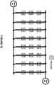
- Figure 2depicts a schematic diagram of a signal distribution system consisting of the network configuration of Figure 1 and a number (subject to a maximum practical limit - to be explained below) of substantially identical circuit blocks called "Arrival-Time-Averaging Client" or ATAC circuits attached to the network.
- the block 5represents one of the ATAC circuits in Figure 2 .
- Other ATAC circuits in Figure 2are labeled A, B, D, Z, AA, and AF.
- Each ATAC circuithas two inputs and one output as shown in Figure 3 .
- the ATAC circuit inputsare connected to the branches of the branch pairs at adjacent positions. Some of the ATAC circuits may be connected in reverse order than others. For example, if the "normal" connection order is defined as first input of the ATAC circuit attached to the first tree network and second input of the ATAC circuit attached to the second tree network, then some of the ATAC circuits may be connected with their first input attached to the second tree network and their second inputs attached to the first tree network.
- the ATAC circuitsare assumed not to load the transmission lines forming the tree branches in any significant way. In other words, the signals traveling on each tree are assumed undisturbed by the presence of the ATAC circuits.
- the input impedance of the ATAC circuitsis assumed large with respect to the characteristic impedance of the transmission lines such that the ATAC circuits just sense the voltages or currents on the branches with no significant effects in the tree signals. This assumption is reasonable in practice if the number of ATAC circuits is not excessive. This explains the earlier comment regarding the maximum practical limit for the number of ATAC circuits.
- the functionality of the ATAC circuitis explained in Figure 3 for the case when the generator signals are periodic pulses (zero modulation). In general, these pulses arrive at the two ATAC circuit inputs at different times.
- the ATAC circuitgenerates output pulses in the middle of the period between the two input pulses, hence the name of the circuit. In other words, the ATAC circuit output pulses are placed at the average time between the arrival times of the input pulses.
- the functionality of the ATAC circuit for the case of periodic pulsesis described as in the clock extracting circuits in more detail in Wayne D. Grover "Method and Apparatus for Clock Distribution and for Distributed Clock Synchronization" U.S. Patent No. 5,361,277, Nov.
- the outputs of the ATAC circuits in the system of Figure 2have phase synchronous carriers. For simplicity, consider the case of generator signals, which are periodic and have no modulation.
- the system in Figure 2is also shown in Figures 4-6 , with different signal propagation paths and times specifically indicated.
- the ATAC circuits labeled A, B, C, Z, AA, AF,will be referred as Client A, B, C, etc.
- the signal propagating times from the tree inputs to Client Bare TB1 and TB2.
- SFTSynchronization Flight Time
- Figure 6focuses on calculating the SFT of the branch pair on the far right with respect to the SFT of the branch pair on the far left. This calculation is straightforward if one assumes that a client existed on the far right branch pair at the same relative position in its branch pair as Client B is on the far left branch pair. This imaginary client for purposes of illustration is referred to as Virtual Client B'. Based on the previous discussion, the SFT of Virtual Client B' is a constant for the far right branch pair.
- ⁇ T2 in relations (4)is the signal travel time on the tree trunks for the trunk pair section connecting the two branch pairs under consideration (far left and far right).
- ⁇ T2represents the time necessary for the signals to travel over this translation.
- Figure 7shows the instances these pulses arrive at positions B, D, and B'.
- the pulses shown in solid linesoriginate from Generator #1 and the pulses shown in dotted lines originate from Generator #2.
- the average pulse arrival timeis an absolute time instance equal to half the value of SFT (assuming time zero is defined at the instance when pulses are generated by the generator). Therefore, all Client outputs are in precise phase synchronization. This property is independent of the pulse generation times, as it can be easily verified with the help of the diagrams in Figure 7 .
- the relative positions of the pulses originating from each generatordepend only on the quantities ⁇ T1 and ⁇ T2, which are system invariants, i.e., quantities set by the system configuration. These invariants determine an inherent symmetry between the pulses coming from the Generator #1 and those coming from the Generator #2 on the time coordinate. This symmetry determines the global reference extracted by the ATAC circuits.
- the Generator #2is phase modulated with a signal whose bandwidth is much smaller than the carrier frequency.
- the carrier frequencyis 1 GHz and the modulating signal bandwidth is 1KHz.
- the modulation signalsis a general random signal with 1 KHz bandwidth, the rate of change of the modulation signals is even smaller.
- the addition of this modulationwill change the pulse diagrams by moving the dotted pulses in Figure 8 back and forth very slowly over thousands of pulses.
- Figure 8illustrates the peak-to-peak ⁇ T phase variation of the pulses coming from generator #2.
- the Client outputscontain the same modulation reduced by a factor of two, due to averaging with a zero modulation signal (from Generator #1).
- the propagation of the modulated signal along the transmission lines from Generator #2 to any Clienthas the same speed as the carrier propagation. Therefore, each Client will receive this signal with an appropriate delay.
- the signal propagation time from the generators to the farthest Clientis very short with respect to the modulation autocorrelation width (i.e., inverse of modulation bandwidth). Therefore, from a practical point of view all Clients receive modulated signals instantaneously.
- both generator signals in Figure 2are angle modulated, the Client outputs contain an average angle modulation.
- An important caseis when the two generators are modulated by opposite angle directions.
- the output Client average modulationbecomes zero (carrier only outputs) despite the fact that each tree carries modulated signals. This is an important case for VLSI clock distribution, where EMI is a potential problem.
- embodiments of the present inventioncontemplate distributing modulated signals with a broader energy distribution for lower EMI but still recover pure clock signals at the client outputs.
- Figure 9depicts the ATAC circuit functionality, which still achieves global output phase synchronization.
- SFTis a system invariant. Therefore, any function of SFT is also an invariant. For this reason, in general one can use any client circuit producing an output, which is a function of SFT, to obtain global phase synchronization.
- functionhere refers not to any specific formula but rather to the general mathematical concept associating a single value for every element (e.g., number) from a fixed set.
- a circuit implementing a function of SFTis called Synchronization Client or "S-Client".
- S-ClientFor example, the S-Client functionality in Figure 9 adds a constant time delay to the average pulse-arrival-time.
- ATAC circuitsare particular cases of all possible S-Clients.
- the constant time delay ⁇ Tmay be derived from the period of the pulse trains traveling over the two networks.
- S-Clientsfor the case when sinusoidal signals are used as analog multipliers can be found in NRAO, A Proposal for a Very Large Array Radio Telescope, Vol. II, National Radio Astronomy Observatory, Green Bank, West Virginia, Ch. 14, 1967 ; and Richard R Goulette "Technique for Distributing Common Phase Clock Signals" U.S, Patent No. 6,531,358 B1, May 13, 2003 .
- Other examplesinclude analog multipliers with phase offsets.
- the system in Figure 2has yet another important potential capability, i.e., the possibility of individually shifting the phases of client outputs with respect to the carrier.
- This can be accomplishedOne way is to use different S-Clients, which would implement different functions of SFT, still preserving an underlying absolute time reference. For example, one could use DLL clients with variable locking positions with respect to the input pulses.
- a second method for phase shifting the client outputsis by introducing delays or phase shifts at the branch or trunk coupling. This would give the capability of shifting the extracted carrier phase for a whole branch with respect to other branches. This may be useful in antenna array applications, e.g., for azimuth or altitude only beam steering.
- Figures 10-16depict a non-exhaustive list of examples.
- Figures 10-13show systems using a single generator. In these cases, the second trees are connected to the trunks of the respective first trees.
- Figures 14-16show cases of systems only with trunks and no branches.
- Embodiments of the present inventioninclude many advantages over the disclosed related art. For example, instead of being restricted to using simple serial connections, embodiments of this invention use specially designed tree networks. The replacement of pure serial links with these tree networks accomplishes a great reduction in total transmission line length, with a similar reduction of the signal loss. This is particularly important in VLSI applications, where it is difficult to design very long low-loss transmission lines of small widths and reasonably high characteristic impedance.
- the use of trees as contemplated by embodiments of the present inventionis different from the use of trees in the classical signal distribution because at least there is no requirement for equal time of flight from the tree root to the top of the tree and there are no geometrical restrictions.
- embodiments of the present inventioncontemplate using signals containing a carrier frequency, including non-periodic signals. This is important for the distribution or generation of carrier-synchronized modulated signals such as in active array transmitters. In addition, this has an application in VLSI clock distribution with low EMI
- SFTis identified as the fundamental system invariant and the fundamental absolute time unit. All synchronization aspects are derived from SFT. As a result, any function of SFT provides a valid timing reference. Related art recognized only the time arrival average as an absolute time reference. Therefore, embodiments of the present invention show a more general principle for the synthesis of synchronized carrier circuits.
- FIG. 17-18A first generalization possibility of the system in Figure 2 is shown graphically in Figures 17-18 .
- the trunksAs in Figure 17 are shown graphically in Figures 17-18 .
- One effect of changing the trunk length or even distorting their physical shapes (as long as both trunks have the same section lengths)is a global timing reference shift.
- Figure 18the same is true if all branches are distorted in length and shape.
- FIGS 19-20show embodiments of the present invention.
- FIG 19there is depicted two trees, not equal in general, each tree having one trunk and any number of branches connected in any number of levels.
- a generatorexcites each tree trunk.
- Each phase synchronization pairhas a unique SFT.
- Figure 20shows the addition of S-Client circuits to the network in Figure 19 such that the SFT is used to extract an absolute time reference (generate signals with phase synchronous carriers).
- an absolute time referencegenerator signals with phase synchronous carriers.
- one generatormay be eliminated and the second tree coupled to the first tree.
- Figure 21The only difference between the cases in Figures 19-21 and the previous cases is that the S-Client circuits must have additional physical means to tap the signals on the phase synchronization pairs, as the respective tree branches may not be close to the each other in general. Therefore, the S-Client circuits are required to have long enough input terminals to reach all points, as necessary.
- a practical way to substantially ensure the phase synchronization pairs contain points close to each otheris shown in Figure 22 for just one pair of branches. The considered branch of the second tree is folded and placed in close proximity with the considered branch of the first tree.
- the general system in Figures 19-20may be used to generate signals with phase synchronous carrier based only on a subset of points.
- the same network configurationis capable of generating many sets of carrier-synchronized outputs, each set using a specific collection of phase synchronization pairs.
- the network of Figure 2 and the others based on itare special cases where all adjacent points on the tree branches placed next to each other form a collection of phase synchronization pairs.
- Three-dimensional extensions called Cartesian systemsare shown in Figure 23 using two generators and in Figure 24 using a single generator. In a consistent manner with this definition, the system of or Figure 2 or Figure 12 , etc. are two-dimensional Cartesian systems.
- Collections of phase synchronization points with different SFTscan yield identical S-Client outputs.
- S-clientsare analog multipliers (sinusoidal signals case)
- all collections of phase synchronization points with SFTs, which are different by an integer number of the signal periodgenerate identical S-Client outputs. The reason for this is that the waves propagating on the two tree networks create periodic signals in space as well as in time.
- the phase synchronization pairscan be selected not on the basis of signal travel times as before but rather on a specific relationship between the signal phases.
- a relationshipcould be a constant average phase.
- the two networkscould be any networks not necessarily tree networks.
- Figure 26shows this general case, where the point pairs (a1, a2), (b1, b2), (c1,c2), and (d1,d2) are selected such that the signal phases add to a constant or have a constant average, etc.
- the S-Clientscould be analog multipliers.
- the outputs of the S-Clientsare phase synchronized carriers.
- Figure 27shows this embodiment of the present invention with a single generator, where one of the networks is excited by a signal tapped from the other network.
- inventions of the present inventioncontemplate obtaining globally synchronized frequency conversion of many RF signals without explicitly generating synchronized LO (local oscillator) signals.
- Figure 25shows such a case.
- the RF signalsare first multiplied by a first signal in a first LO trunk and the resulting signal is further multiplied by the second signal in the second LO trunk.
- Some filteringmay be necessary. All IF signals produced are globally synchronized with respect to the original RF signals, just as if the RF signals had been mixed with a global reference. This concept is also application for any tree networks as in the previous cases.
Landscapes
- Engineering & Computer Science (AREA)
- Theoretical Computer Science (AREA)
- Computer Networks & Wireless Communication (AREA)
- Signal Processing (AREA)
- Physics & Mathematics (AREA)
- General Engineering & Computer Science (AREA)
- General Physics & Mathematics (AREA)
- Synchronisation In Digital Transmission Systems (AREA)
- Digital Transmission Methods That Use Modulated Carrier Waves (AREA)
- Position Fixing By Use Of Radio Waves (AREA)
Description
- Embodiments of the present invention generally relate to analog and digital signal distribution/synchronization methods and systems and in particular to the distribution of sinusoidal signals in a coherent system to achieve carrier phase/frequency synchronization at the distribution points.
- Many analog and digital systems and subsystems used in communications, computing, data processing, military, and other applications (collectively hereinafter referred to as "coherent systems") are designed to operate synchronously. Typical coherent systems comprise subsystems capable of generating and transmitting signals such as electronic, electrical, mechanical, optical, or sonar subsystems. An example of an electronic coherent system is the massive set of logic gates present in modern digital systems or subsystems. These gates switch according to an absolute clock beat, which is provided by properly generated or distributed clock signals. Typically, the local clock signals are distributed from a master clock source. In order to reduce system level EMI (electromagnetic interference), this clock signal is sometimes modulated with low frequency signals or noise. For example, this technique is often used in VLSI systems. In such a case, the distributed "clock" signal is a phase-modulated carrier, which is non-periodic, albeit with approximately periodic shape over short time intervals. The distribution network must guarantee accurate carrier synchronization such that all logic is clocked properly from clock beat to clock beat, even though in the long run the phase of the clock signal wanders around an average absolute value.
- In addition to digital applications, there are many analog, RF, and mixed-signal systems, which require time synchronization of modulated signals. For example, active arrays, such as phased-array radars or electronic steering antennas rely on precise carrier phasing of RF signals. The distribution of these modulated signals is similar in concept to the clock distribution in digital systems.
- A typical signal distribution network with phased aligned outputs is built hierarchically using a tree topology, starting with a master generator connected to a tree trunk to which branches are attached, followed by other branches, etc. until the final signal delivery points are reached on top of the tree. If the distribution network is electrically small for the carrier frequency used, i.e., if the signal propagation times from the generator to any of the final delivery points are small compared to the carrier period, the tree network as described without any additional constraints is adequate. However, in most modern applications, the carrier frequencies are so high (e.g., on the order of GHz) that even miniaturized systems, such as fully integrated circuits, are not electrically small. In such cases, the design of the distribution network providing accurate synchronization may become extremely challenging.
- A known approach to signal distribution in electrically-large systems is based on the "equal time-of-flight" principle. The distribution network is designed such that the time necessary for a signal to propagate from the master generator to all delivery points at the top of the tree is a constant. The RF corporate feed network or the VLSI H-tree clocking network are typical examples implementing this principle. This approach is the de facto "work horse" of signal distribution/synchronization but suffers from well-documented practical limitations: stringent geometrical constraints, power hungry, susceptibility to noise, and susceptibility to timing errors known as skew. Often, expensive additional techniques are employed to contain these shortcomings. In the case of active distribution trees, such as those used in VLSI clocking, operation at frequencies above a few GHz is rather difficult to attain. Recently, serial clock distribution over wave guides has been proposed, motivated by improved theoretical performance in power dissipation, noise and cost. For example, see Wayne D Grover "Method and Apparatus for Clock Distribution and for Distributed Clock Synchronization,"
U.S. Pat. No. 5,361,277, Nov. 1, 1994; Michael Farmwald and Mark Horowitz , "Apparatus for Synchronously Generating Clock Signals in a Data Processing System"U.S. Pat. No. 5,243,703, Sept. 7, 1993; Charles D. Miller "Signals Distribution System"U.S. Pat. No. 5,712,882, Jan. 27, 1998 ;NRAO, A Proposal for a Very Large Array Radio Telescope, Vol. II, National Radio Astronomy Observatory, Green Bank, West Virginia, Ch. 14, 1967; Richard R Goulette "Technique for Distributing Common Phase Clock Signals"U.S, Pat. No. 6,563,358 B1, May 13, 2003 ; andV. Prodanov and M. Banu "GHz Serial Passive Clock Distribution in VLSI Using Bidirectional Signaling," Proceedings, 2006 IEEE Custom Integrated Circuits Conference. The inherent skew accumulation due to serial transmission is mitigated by time averaging two signals propagating in opposite directions. The main fundamental shortcomings of this technique are a) the large total length of the waveguides, possibly resulting in signal loss and dispersion, and b) the limited practical precision of the known time averaging circuits. In addition, these methods were intended for distribution of periodic, not modulated, signals. - A first class of previously proposed serial clock distribution schemes: See Wayne D. Grover "Method and Apparatus for Clock Distribution and for Distributed Clock Synchronization"
U.S. Pat. No. 5,361,277, Nov. 1, 1994 ; Michael Farmwald and Mark Horowitz, "Apparatus for Synchronously Generating Clock Signals in a Data Processing System"U.S. Pat. No. 5,243,703, Sept. 7, 1993 ; and Charles D. Miller "Signals Distribution System"U.S. Pat. No. 5,712,882, Jan. 27, 1998 , uses electrical pulse signaling over transmission lines. For these techniques, any pulse dispersion introduces timing errors, which increase as the pulses travel farther and farther away from the generators. The theoretical possibilities to avoid these errors at high frequencies are either to use extremely good, low-dispersion transmission lines, or to keep the total length of the transmission lines short. The first option increases the system cost and the second option reduces the number of useful applications. Applying this approach with high speed optical pulses transmitted over optical wave-guides should provide significantly lower dispersion but such systems would require additional error-prone functionality related to optical-to-electrical conversion. - A second class of proposed serial clock distribution schemes, seeNRAO, A Proposal for a Very Large Array Radio Telescope, Vol. II, National Radio Astronomy Observatory, Green Bank, West Virginia, Ch. 14, 1967; Richard R Goulette "Technique for Distributing Common Phase Clock Signals"
U.S, Pat. No. 6,531,358 B1, May 13, 2003 ; andV. Prodanov and M. Banu "GHz Serial Passive Clock Distribution in VLSI Using Bidirectional Signaling," Proceedings, 2006 IEEE Custom Integrated Circuits Conference, use electrical sinusoidal excitations over transmissions lines and analog multipliers for time averaging. One advantage of single tone signaling is the elimination of dispersion as a negative factor in system performance. Moreover, the use of multipliers seems attractive due to the apparent simplicity of this scheme. However, this theoretical simplicity is deceptive. - On a closer analysis, it becomes clear that the precision of the overall scheme depends on the quality of the analog multipliers that can be realized in practice. Of particular relevance is the multiplier output harmonic purity. Typical high frequency multiplier circuits such as those used as RF mixers generate outputs rich in harmonics. Such circuits cannot be used for accurate time averaging because the output harmonics introduce significant timing errors. Therefore, special analog multiplier circuits with low harmonic output content are needed. This is not a trivial design task for low cost applications such as VLSI clocking, where using integrated RF filters to clean up each multiplier output would not be economical. The design of integrated multipliers with very low harmonic content is further complicated if the two multiplier inputs do not have the same magnitude. Therefore, in practice, the signal loss over the transmission lines must be maintained low. Just as before, this limits the technique either in terms of cost through the requirement of implementing expensive low-loss transmission lines, or in limited application possibilities due to short total transmission line length.
US 6323716 B1 relates to a signal distributing circuit that includes a first element which outputs a first signal and a second signal which is opposite to that of the first signal. The circuit is provided with a first signal line on which the first signal is transmitted and a second signal line on which the second signal is transmitted. A plurality of second elements each of which is connected to the first signal line in a first order and connected to the second signal line in a second order, wherein the second order is opposite to that of the first order. A method for connecting a plurality of loads to first and second signal lines, which are allocated to a regular signal and a signal opposite to that of the regular signal, respectively, of the invention includes connecting the loads to the first signal lines in a first order; and connecting the loads to the second signal lines in an order opposite to that of the first order.- The conventional tree (i.e., corporate feed) distribution scheme and the purely serial distribution scheme represent two cases. Embodiments of the present invention include a method and system that approaches the merits of the purely serial scheme without requiring excessive transmission line lengths. Embodiments of the present invention may use modulated signals rather than pure tones for widest possible applications.
Aspects and embodiments of the invention are set out in the appended claims. - So the manner in which the above recited features of the present invention can be understood in detail, a more particular description of embodiments of the present invention, briefly summarized above, may be had by reference to embodiments, which are illustrated in some of the appended drawings. It is to be noted, however, these drawings illustrate only typical embodiments encompassed within the scope of the present invention, and, therefore, are not to be considered limiting, for the present invention may admit to other equally effective embodiments, wherein:
Figure 1 depicts a schematic diagram of a synchronization system having two independent tree networks with paired branches, excited by two independent generators;Figure 2 depicts a schematic diagram of the tree networks of the synchronization system ofFigure 1 with Arrival-Time-Averaging Client (ATAC) circuits placed on the branch pairs;Figure 3 illustrates a timing diagram and the functionality of an ATAC circuit where generator signals contain pulses;Figure 4 depicts a schematic diagram of the synchronization system ofFigure 2 , illustrating travel times TB1 and TB2 from the two generators to ATAC circuit B and defines the system quantity SFT (Synchronization Time Flight) as the sum of TB1 and TB2;Figure 5 depicts a schematic diagram of the synchronization system ofFigure 2 , illustrating the travel times TD1 and TD2 from the two generators to ATAC circuit D and shows their sum TD1+TD2 equals SFT;Figure 6 depicts a schematic diagram of a synchronization system, illustrating the travel times TB'1 and TB'2 from the two generators to virtual ATAC circuit B' and shows their sum TB'1+TB'2 equals SFT;Figure 7 illustrates a timing diagram of the synchronization system ofFigure 6 , depicting the arrival pulse times at client B, client D, and virtual client B' fromFigure 6 , assuming both generators send pulses at time equal zero, demonstrating that the arrival time average is the same for all cases and is a function of SFT;Figure 8 illustrates a timing diagram of the synchronization system ofFigure 6 , depicting the effect ofGenerator # 2 angle modulation with δT peak-to-peak phase variation;Figure 9 illustrates a timing diagram and the functionality of a general S-Client circuit, whose output is a function of SFT and where the functionality is more general than that of any ATAC circuit;Figure 10 illustrates a schematic diagram of a synchronization system having a single generator;Figure 11 illustrates a schematic diagram of a synchronization system having a single generator;Figure 12 illustrates a schematic diagram of a synchronization system having physically separated tree trunks depicting a two dimensional Cartesian system;Figure 13 illustrates a schematic diagram of a synchronization system having a a Cartesian system with physically separated tree trunks;Figures 14 illustrates a schematic diagram of a synchronization system having no tree branches and two generators, one generator being modulated ;Figures 15 illustrates a schematic diagram of a synchronization system having no tree branches and two generators, both generators being modulated ;Figures 16 illustrates a schematic diagram of a synchronization system having no tree branches and a single modulated generator;Figures 17 depicts a schematic diagram of the synchronization system ofFigure 2 with "distorted" trunks;Figures 18 depicts a schematic diagram of the synchronization system ofFigure 2 with "distorted" trunks and branches;Figure 19 depicts a schematic diagram of a synchronization system having two general tree networks with sensing points chosen such as to create Phase Synchronization Pairs (a1, a2), (b1, b2), (c1, c2)... (n1, n2);Figure 20 depicts a schematic diagram of the tree networks fromFigure 19 with S-Client circuits added at the points of the Phase Synchronization Pairs (a1, a2), (b1, b2), (c1, c2), (n1, n2) ;Figure 21 depicts a schematic diagram of the general signal distribution principle ofFigure 20 using a single generator ;Figure 22 depicts a schematic diagram of a method to implement the system ofFigure 20 having close points in all Phase Synchronization Pairs;Figure 23 depicts a schematic diagram of a three dimensional Cartesian synchronization system having two generators;Figure 24 depicts a schematic diagram of a three dimensional Cartesian synchronization system having a single generator;Figure 25 depicts a schematic diagram of a double-conversion system with globally synchronized bi-directional local oscillator (LO) signals;Figure 26 depicts a schematic diagram of a synchronization system with two networks of any topology and phase synchronization pairs (a1,a2), (b1,b2), (c1,c2), (d1,d2) selected based on signal phase relationships; andFigure 27 depicts a schematic diagram of the synchronization system ofFigure 26 with a single generator.- The headings used herein are for organizational purposes only and are not meant to be used to limit the scope of the description or the claims. As used throughout this application, the word "may" is used in a permissive sense (i.e., meaning having the potential to), rather than the mandatory sense (i.e., meaning must). Similarly, the words "include", "including", and "includes" mean including but not limited to. To facilitate understanding, like reference numerals have been used, where possible, to designate like elements common to the Figures.
- Embodiments of the present invention include the generation of at least two modulated signals at many points in space such that their carriers have the same frequency and are in precise phase relationship to each other.
Figure 1 depicts a schematic diagram of two independent tree networks, each consisting of atree trunk 1 andtree branches 2. The tree trunk and the tree branches are properly terminated transmission lines (termination circuits are not shown inFigure 1 for simplicity), such as electrical microstrip lines, optical wave-guides, or sound propagating guides. The difference between thetrunk 1 and thebranches 2 is not in substance but rather in name, based on the relative position of the transmission lines (TL) with respect to the tree network input port. Thetrunk 1 is defined as the transmission line connected directly to the input port. Thebranches 2 are coupled to thetrunk 1 through passive oractive circuits 3. A passive coupling circuit could be a simple signal splitter. An active coupling circuit in the case of electrical systems could be a voltage amplifier sensing the voltage of the trunk at the coupling point and driving the branch. The signal delays through these coupling circuits are assumes either identical for all coupling circuits or in known relationships to each other. For simplicity and clarity, the tree network drawings inFigure 1 and the tree network drawings in all other Figures of this specification show no termination circuits explicitly. Nevertheless, it is to be understood that all network trunks and branches are properly terminated (with simple resistors or more involved networks) in order to avoid any significant signal reflections.- The tree networks described with regard to
Figure 1 are particular cases of a larger class of tree networks referred to in this specification as TL-tree networks. In general, a TL-tree network has a trunk, which is a TL coupled to the TL-tree input, and many branches, which are TLs coupled either to the trunk or to other branches. The level of the TL-tree network is the largest number of branches through which a signal applied at the TL-tree input travels plus one (counting the trunk as a branch). For example, the TL-trees inFigure 1 are two-level trees (input signals travels through one trunk and one branch). Hereinbelow, examples are provided of TL-trees with levels larger than two (e.g.,Figures 19-20 ). It should be understood that embodiments of the present invention contemplate TL-tree networks but also many tree networks, which are not TL-tree networks. For example, the trunk and some or all of the branches may be constructed without TLs. The use of TL components is not critical. - The two tree networks in
Figure 1 have parallel trunks and their branches are paired such that all pairs4 have substantially identical physical structure. The position where each branch pair connects to the parallel trunks is not critical. The two branches in every pair are in close proximity to each other. - Two
generators 5 apply input signals to the tree networks inFigure 1 . The generator signals may be modulated carriers of frequency f. A carrier is any periodic signal when modulation is not presents (zero modulation) and the carrier frequency is the frequency of the carrier when modulation is not present. When modulation is present, such as phase or frequency modulation, the carrier is usually not a periodic signal. Figure 2 depicts a schematic diagram of a signal distribution system consisting of the network configuration ofFigure 1 and a number (subject to a maximum practical limit - to be explained below) of substantially identical circuit blocks called "Arrival-Time-Averaging Client" or ATAC circuits attached to the network. Theblock 5 represents one of the ATAC circuits inFigure 2 . Other ATAC circuits inFigure 2 are labeled A, B, D, Z, AA, and AF.- Each ATAC circuit has two inputs and one output as shown in
Figure 3 . The ATAC circuit inputs are connected to the branches of the branch pairs at adjacent positions. Some of the ATAC circuits may be connected in reverse order than others. For example, if the "normal" connection order is defined as first input of the ATAC circuit attached to the first tree network and second input of the ATAC circuit attached to the second tree network, then some of the ATAC circuits may be connected with their first input attached to the second tree network and their second inputs attached to the first tree network. - The ATAC circuits are assumed not to load the transmission lines forming the tree branches in any significant way. In other words, the signals traveling on each tree are assumed undisturbed by the presence of the ATAC circuits. As a further clarification, if the system in
Figure 2 is purely electrical, the input impedance of the ATAC circuits is assumed large with respect to the characteristic impedance of the transmission lines such that the ATAC circuits just sense the voltages or currents on the branches with no significant effects in the tree signals. This assumption is reasonable in practice if the number of ATAC circuits is not excessive. This explains the earlier comment regarding the maximum practical limit for the number of ATAC circuits. - The functionality of the ATAC circuit is explained in
Figure 3 for the case when the generator signals are periodic pulses (zero modulation). In general, these pulses arrive at the two ATAC circuit inputs at different times. The ATAC circuit generates output pulses in the middle of the period between the two input pulses, hence the name of the circuit. In other words, the ATAC circuit output pulses are placed at the average time between the arrival times of the input pulses. The functionality of the ATAC circuit for the case of periodic pulses is described as in the clock extracting circuits in more detail in Wayne D. Grover "Method and Apparatus for Clock Distribution and for Distributed Clock Synchronization"U.S. Patent No. 5,361,277, Nov. 1, 1994 ; Michael Farmwald and Mark Horowitz, "Apparatus for Synchronously Generating Clock Signals in a Data Processing System"U.S. Pat. No. 5,243,703, Sept. 7, 1993 ; and Charles D. Miller "Signals Distribution System"U.S. Pat. No. 5,712,882, Jan. 27, 1998 . Practical implementations include PLL and DLL circuits. - The outputs of the ATAC circuits in the system of
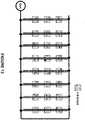
Figure 2 have phase synchronous carriers. For simplicity, consider the case of generator signals, which are periodic and have no modulation. The system inFigure 2 is also shown inFigures 4-6 , with different signal propagation paths and times specifically indicated. The ATAC circuits labeled A, B, C, Z, AA, AF, will be referred as Client A, B, C, etc. - In
Figure 4 , the signal propagating times from the tree inputs to Client B are TB1 and TB2. We define a parameter called "Synchronization Flight Time" or SFT as the sum of TB1 and TB1:
Figure 5 shows the signal paths to Client D and the associated signal travel times TD1 and TD2. These two quantities can be expressed in terms of TB1 and TB2 as follows:

- The quantity ΔT1 in relations (2) is the signal travel time on the tree branches between the positions of Clients B and D (
Figure 5 ). Adding relations (2) and using (1), we have:
- The relation (3) was derived without any specific assumptions regarding the position of Client D on its branch pair. Therefore, for the branch pair considered, SFT is a constant. By similar arguments, all branch pairs have a constant SFT. Furthermore, we can show that the SFT of all branch pairs have the same value, and therefore SFT is a system constant. This will be done next.
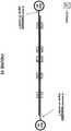
Figure 6 focuses on calculating the SFT of the branch pair on the far right with respect to the SFT of the branch pair on the far left. This calculation is straightforward if one assumes that a client existed on the far right branch pair at the same relative position in its branch pair as Client B is on the far left branch pair. This imaginary client for purposes of illustration is referred to as Virtual Client B'. Based on the previous discussion, the SFT of Virtual Client B' is a constant for the far right branch pair. The travel times of signals from the generators to the position of Virtual Client B' are calculated, TB'1 and TB'2 as:

- The quantity ΔT2 in relations (4) is the signal travel time on the tree trunks for the trunk pair section connecting the two branch pairs under consideration (far left and far right). A different way of explaining this is to notice the far right branch pair can be regarded as a translation in space of the far left branch pair and ΔT2 represents the time necessary for the signals to travel over this translation. Adding relations (4) results in SFT being a system constant:

- It can be concluded that for the distribution system in
Figure 2 , all Clients (ATAC circuits) placed at any arbitrary positions on the branch pairs detect signals whose combined total travel time from their respective generators is a constant (SFT). The significance of this property is illustrated inFigure 7 . - Assuming the generator signals are periodic pulses originating at time zero,
Figure 7 shows the instances these pulses arrive at positions B, D, and B'. The pulses shown in solid lines originate fromGenerator # 1 and the pulses shown in dotted lines originate fromGenerator # 2. The average pulse arrival time is an absolute time instance equal to half the value of SFT (assuming time zero is defined at the instance when pulses are generated by the generator). Therefore, all Client outputs are in precise phase synchronization. This property is independent of the pulse generation times, as it can be easily verified with the help of the diagrams inFigure 7 . The relative positions of the pulses originating from each generator depend only on the quantities ΔT1 and ΔT2, which are system invariants, i.e., quantities set by the system configuration. These invariants determine an inherent symmetry between the pulses coming from theGenerator # 1 and those coming from theGenerator # 2 on the time coordinate. This symmetry determines the global reference extracted by the ATAC circuits. - The previous discussions show that although the Clients in the system of
Figure 2 are positioned at different coordinates in space, their outputs are in precise phase alignment if the inputs are periodic signals, i.e. un-modulated carriers. The addition of angle modulation whose bandwidth is small with respect to the carrier, does not change the practical system behavior in any significant way.Figure 8 demonstrates this graphically. - In
Figure 8 , it is assumed that theGenerator # 2 is phase modulated with a signal whose bandwidth is much smaller than the carrier frequency. For example, the carrier frequency is 1 GHz and the modulating signal bandwidth is 1KHz. In this case, there are 100000 carrier cycles in each modulating signal cycle for 1 KHz sinusoidal modulation. If the modulation signals is a general random signal with 1 KHz bandwidth, the rate of change of the modulation signals is even smaller. The addition of this modulation will change the pulse diagrams by moving the dotted pulses inFigure 8 back and forth very slowly over thousands of pulses.Figure 8 illustrates the peak-to-peak δT phase variation of the pulses coming fromgenerator # 2. The Client outputs contain the same modulation reduced by a factor of two, due to averaging with a zero modulation signal (from Generator #1). - In general, the propagation of the modulated signal along the transmission lines from
Generator # 2 to any Client has the same speed as the carrier propagation. Therefore, each Client will receive this signal with an appropriate delay. However, in many practical instances of interest the signal propagation time from the generators to the farthest Client is very short with respect to the modulation autocorrelation width (i.e., inverse of modulation bandwidth). Therefore, from a practical point of view all Clients receive modulated signals instantaneously. - If both generator signals in
Figure 2 are angle modulated, the Client outputs contain an average angle modulation. An important case is when the two generators are modulated by opposite angle directions. The output Client average modulation becomes zero (carrier only outputs) despite the fact that each tree carries modulated signals. This is an important case for VLSI clock distribution, where EMI is a potential problem. Instead of distributing pure periodic signals with concentrated energy at one frequency and harmonics, embodiments of the present invention contemplate distributing modulated signals with a broader energy distribution for lower EMI but still recover pure clock signals at the client outputs. Figure 9 depicts the ATAC circuit functionality, which still achieves global output phase synchronization.. SFT is a system invariant. Therefore, any function of SFT is also an invariant. For this reason, in general one can use any client circuit producing an output, which is a function of SFT, to obtain global phase synchronization. For clarity, the term "function" here refers not to any specific formula but rather to the general mathematical concept associating a single value for every element (e.g., number) from a fixed set.- A circuit implementing a function of SFT is called Synchronization Client or "S-Client". For example, the S-Client functionality in
Figure 9 adds a constant time delay to the average pulse-arrival-time. ATAC circuits are particular cases of all possible S-Clients. A simple S-Client, which is not an ATAC circuit, would be a DLL (Delay Locked Loop) locking at a constant time offset from the average pulse arrival times, as per functionality inFigure 9 . The constant time delay ΔT may be derived from the period of the pulse trains traveling over the two networks. Other examples of S-Clients for the case when sinusoidal signals are used as analog multipliers can be found inNRAO, A Proposal for a Very Large Array Radio Telescope, Vol. II, National Radio Astronomy Observatory, Green Bank, West Virginia, Ch. 14, 1967; and Richard R Goulette "Technique for Distributing Common Phase Clock Signals"U.S, Patent No. 6,531,358 B1, May 13, 2003 . Other examples include analog multipliers with phase offsets. - The system in
Figure 2 has yet another important potential capability, i.e., the possibility of individually shifting the phases of client outputs with respect to the carrier. There are two ways this can be accomplished. One way is to use different S-Clients, which would implement different functions of SFT, still preserving an underlying absolute time reference. For example, one could use DLL clients with variable locking positions with respect to the input pulses. A second method for phase shifting the client outputs is by introducing delays or phase shifts at the branch or trunk coupling. This would give the capability of shifting the extracted carrier phase for a whole branch with respect to other branches. This may be useful in antenna array applications, e.g., for azimuth or altitude only beam steering. - The system in
Figure 2 can be extended into many variations.Figures 10-16 depict a non-exhaustive list of examples.Figures 10-13 show systems using a single generator. In these cases, the second trees are connected to the trunks of the respective first trees.Figures 14-16 show cases of systems only with trunks and no branches. - Embodiments of the present invention include many advantages over the disclosed related art. For example, instead of being restricted to using simple serial connections, embodiments of this invention use specially designed tree networks. The replacement of pure serial links with these tree networks accomplishes a great reduction in total transmission line length, with a similar reduction of the signal loss. This is particularly important in VLSI applications, where it is difficult to design very long low-loss transmission lines of small widths and reasonably high characteristic impedance. The use of trees as contemplated by embodiments of the present invention is different from the use of trees in the classical signal distribution because at least there is no requirement for equal time of flight from the tree root to the top of the tree and there are no geometrical restrictions.
- Furthermore, instead of using only periodic signals, embodiments of the present invention contemplate using signals containing a carrier frequency, including non-periodic signals. This is important for the distribution or generation of carrier-synchronized modulated signals such as in active array transmitters. In addition, this has an application in VLSI clock distribution with low EMI
- SFT is identified as the fundamental system invariant and the fundamental absolute time unit. All synchronization aspects are derived from SFT. As a result, any function of SFT provides a valid timing reference. Related art recognized only the time arrival average as an absolute time reference. Therefore, embodiments of the present invention show a more general principle for the synthesis of synchronized carrier circuits.
- A first generalization possibility of the system in
Figure 2 is shown graphically inFigures 17-18 . Starting with the original system inFigure 2 one can distort the trunks as inFigure 17 with no consequences to the carrier synchronization of the client outputs. This is further illustrated based on the previous discussion regardingFigures 4-6 . One effect of changing the trunk length or even distorting their physical shapes (as long as both trunks have the same section lengths) is a global timing reference shift. Similarly, as illustrated inFigure 18 the same is true if all branches are distorted in length and shape. - The advantage that the physical shape of the trees is not essential is very valuable in practice and contemplated by the present invention. In the case of array synchronization, embodiments of the present invention contemplate conformal designs. Also, in the case of VLSI clock distribution, no constraints are imposed in terms of TL lengths and shapes, unlike distribution trees such as H-trees.
Figures 19-20 show embodiments of the present invention. InFigure 19 , there is depicted two trees, not equal in general, each tree having one trunk and any number of branches connected in any number of levels. A generator excites each tree trunk. One can choose pairs of tree points such that each pair contains a point from the first tree and a point from the second tree. These pairs are called phase synchronization pairs. Each phase synchronization pair has a unique SFT. In general, one can identify many phase synchronization points with the same SFT. For example, one can chose two points arbitrarily, one on each tree and form a first pair.- For this particular pair, there is a SFT calculated as the sum of the signal propagation time from the
Generator # 1 to the first tree point in the pair with the signal propagation time from theGenerator # 2 to the second tree point in the pair. Next, one can step away from theGenerator # 1 on the first tree and towards theGenerator # 2 on the second tree and find other point pairs with the same SFT. Moreover, one can search other branches and find additional pairs with the same SFT. Clearly, for any dual-tree network, there are many possible SFT and associated sets of tree point pairs. A set of synchronization pairs with the same SFT is called a collection of synchronization pairs.Figure 19 illustrates a collection of three phase synchronization pairs (a1, a2), (b1, b2), and (c1, c2). Figure 20 shows the addition of S-Client circuits to the network inFigure 19 such that the SFT is used to extract an absolute time reference (generate signals with phase synchronous carriers). Naturally, just like before, one generator may be eliminated and the second tree coupled to the first tree. This possibility is shown inFigure 21 . The only difference between the cases inFigures 19-21 and the previous cases is that the S-Client circuits must have additional physical means to tap the signals on the phase synchronization pairs, as the respective tree branches may not be close to the each other in general. Therefore, the S-Client circuits are required to have long enough input terminals to reach all points, as necessary. A practical way to substantially ensure the phase synchronization pairs contain points close to each other is shown inFigure 22 for just one pair of branches. The considered branch of the second tree is folded and placed in close proximity with the considered branch of the first tree.- The general system in
Figures 19-20 may be used to generate signals with phase synchronous carrier based only on a subset of points. In fact, in general the same network configuration is capable of generating many sets of carrier-synchronized outputs, each set using a specific collection of phase synchronization pairs. The network ofFigure 2 and the others based on it are special cases where all adjacent points on the tree branches placed next to each other form a collection of phase synchronization pairs. Three-dimensional extensions called Cartesian systems are shown inFigure 23 using two generators and inFigure 24 using a single generator. In a consistent manner with this definition, the system of orFigure 2 orFigure 12 , etc. are two-dimensional Cartesian systems. - Collections of phase synchronization points with different SFTs can yield identical S-Client outputs. For example, if the S-clients are analog multipliers (sinusoidal signals case), all collections of phase synchronization points with SFTs, which are different by an integer number of the signal period generate identical S-Client outputs. The reason for this is that the waves propagating on the two tree networks create periodic signals in space as well as in time.
- In the previous cases, tree networks without signal reflections, i.e. networks in which the trunk and branches are properly terminated, were considered. This is particularly important in the arrangements using pulse signaling. If signal reflections were allowed, the existence of multiple reflected pulses in the networks could easily impede the operation of the S-Clients. In the case of sinusoidal signaling, the existence of reflections produces only phase and magnitude changes. Assuming there is no use of the points where the signal magnitudes are too small, the phase changes could be mitigated by selecting different taping points on the networks.
- Therefore, in the most general case, the phase synchronization pairs can be selected not on the basis of signal travel times as before but rather on a specific relationship between the signal phases. For example, such a relationship could be a constant average phase. In addition, the two networks could be any networks not necessarily tree networks.
Figure 26 shows this general case, where the point pairs (a1, a2), (b1, b2), (c1,c2), and (d1,d2) are selected such that the signal phases add to a constant or have a constant average, etc. The S-Clients could be analog multipliers. The outputs of the S-Clients are phase synchronized carriers.Figure 27 shows this embodiment of the present invention with a single generator, where one of the networks is excited by a signal tapped from the other network.- In all previous cases, the focus has been in generating globally synchronized carrier signals or clock signals. In certain applications, such as antenna arrays, embodiments of the present invention contemplate obtaining globally synchronized frequency conversion of many RF signals without explicitly generating synchronized LO (local oscillator) signals.
Figure 25 shows such a case. Here, the RF signals are first multiplied by a first signal in a first LO trunk and the resulting signal is further multiplied by the second signal in the second LO trunk. Some filtering (not shown inFigure 25 ) may be necessary. All IF signals produced are globally synchronized with respect to the original RF signals, just as if the RF signals had been mixed with a global reference. This concept is also application for any tree networks as in the previous cases.


Claims (10)
- A method for distributing sinusoidal signals, comprising:applying first and second input sinusoidal signals with carrier frequency f to first and second inputs, respectively, of a system comprising a first tree network coupled to the first input and a second tree network coupled to the second input, the first tree network having a plurality of branches (2) and the second tree network having a plurality of branches (2), the system having a plurality of node pairs each of which includes a first node on a branch of the first tree network and a second node on a branch of the second tree network, each node pair of the plurality of node pairs being at a different location and wherein the first nodes of the plurality of node pairs are located on multiple branches (2) of the first tree network, and wherein the second nodes of the plurality of node pairs are located on multiple branches (2) of the second tree network; andfor each node pair of the plurality of node pairs, processing signals of both the first and second nodes of that pair to generate a corresponding output carrier signal, wherein the output carrier signals for the plurality of node pairs are phase synchronized,wherein each node pair ischaracterized by a synchronization flight time,wherein the synchronization flight time for any node pair of the plurality of node pairs is a sum of the travel time of the first input sinusoidal signal from the first input to the first node of that node pair plus the travel time of the second input sinusoidal signal from the second input to the second node of that node pair, andwherein both of the first and second input sinusoidal signals have periods equal to TD, and wherein the synchronization flight time of each node pair of the plurality of node pairs is equal to SFT + ni·TD, where SFT is the synchronization flight time of a first node pair among the plurality of node pairs, TD is a positive number, where i identifies the node pair, and ni is an integer, wherein not all ni are equal.
- The method of claim 1, wherein processing signals of each node pair of the plurality of node pairs to generate the output carrier signals for the plurality of node pairs involves, for each node pair, analog multiplying the signal of the first node of that node pair with the signal of the second node of that node pair.
- The method of claim 1, wherein the first and second tree networks do not have substantially identical physical structures.
- The method of any preceding claim, wherein the first and second input sinusoidal signals are un-modulated signals.
- The method of any one of claims 1 to 3, wherein the first and second input sinusoidal signals are modulated by opposite angle directions.
- A system for distributing sinusoidal signals, comprising:a first tree network having a first input for receiving a first input sinusoidal signal with carrier frequency f, the first tree network having a plurality of branches (2);a second tree network having a second input for receiving a second input sinusoidal signal with carrier frequency f, the second tree network having a plurality of branches (2);a plurality of node pairs, each of which includes a first node on a branch of the first tree network and a second node on a branch of the second tree network, each node pair of the plurality of node pairs being at a different location and wherein the first nodes of the plurality of node pairs are located on multiple branches (2) of the first tree network, and wherein the second nodes of the plurality of node pairs are located on multiple branches (2) of the second tree network; anda plurality of electronic circuits equal in number to the plurality of node pairs, each electronic circuit of the plurality of electronic circuits for processing signals of both the first and second nodes of a corresponding different node pair of the plurality of node pairs to generate a corresponding output carrier signal, wherein the output carrier signals for the plurality of node pairs are phase synchronized,wherein each node pair ischaracterized by a synchronization flight time,wherein the synchronization flight time for any node pair of the plurality of node pairs is a sum of the travel time of the first input sinusoidal signal from the first input to the first node of that node pair plus the travel time of the second input sinusoidal signal from the second input to the second node of that node pair, andwherein both of the first and second input sinusoidal signals have periods equal to TD, and wherein the synchronization flight time of each node pair of the plurality of node pairs is equal to SFT + ni·TD, where SFT is the synchronization flight time of a first node pair among the plurality of node pairs, TD is a positive number, where i identifies the node pair, and ni is an integer, wherein not all ni are equal.
- The system of claim 6, wherein each electronic circuit of the plurality of electronic circuits comprises an analog multiplier circuit.
- The system of claim 6, wherein the first and second tree networks do not have substantially identical physical structures.
- The system of any one of claims 6 to 8, wherein the first and second input sinusoidal signals are un-modulated signals.
- The system of any one of claims 6 to 8, wherein the first and second input sinusoidal signals are modulated by opposite angle directions.
Applications Claiming Priority (3)
| Application Number | Priority Date | Filing Date | Title |
|---|---|---|---|
| US96136707P | 2007-07-20 | 2007-07-20 | |
| EP08796379AEP2174442A4 (en) | 2007-07-20 | 2008-07-21 | Method and system for multi-point signal generation with phase synchronized local carriers |
| PCT/US2008/070649WO2009015086A2 (en) | 2007-07-20 | 2008-07-21 | Method and system for multi-point signal generation with phase synchronized local carriers |
Related Parent Applications (1)
| Application Number | Title | Priority Date | Filing Date |
|---|---|---|---|
| EP08796379ADivisionEP2174442A4 (en) | 2007-07-20 | 2008-07-21 | Method and system for multi-point signal generation with phase synchronized local carriers |
Publications (3)
| Publication Number | Publication Date |
|---|---|
| EP2840734A2 EP2840734A2 (en) | 2015-02-25 |
| EP2840734A3 EP2840734A3 (en) | 2015-03-18 |
| EP2840734B1true EP2840734B1 (en) | 2019-04-03 |
Family
ID=40282104
Family Applications (3)
| Application Number | Title | Priority Date | Filing Date |
|---|---|---|---|
| EP14190010.0AActiveEP2840734B1 (en) | 2007-07-20 | 2008-07-21 | Method and system for multi-point signal generation with phase synchronized local carriers |
| EP08796379AWithdrawnEP2174442A4 (en) | 2007-07-20 | 2008-07-21 | Method and system for multi-point signal generation with phase synchronized local carriers |
| EP14190013.4AWithdrawnEP2854326A1 (en) | 2007-07-20 | 2008-07-21 | Method and system for multi-point signal generation with phase synchronized local carriers |
Family Applications After (2)
| Application Number | Title | Priority Date | Filing Date |
|---|---|---|---|
| EP08796379AWithdrawnEP2174442A4 (en) | 2007-07-20 | 2008-07-21 | Method and system for multi-point signal generation with phase synchronized local carriers |
| EP14190013.4AWithdrawnEP2854326A1 (en) | 2007-07-20 | 2008-07-21 | Method and system for multi-point signal generation with phase synchronized local carriers |
Country Status (6)
| Country | Link |
|---|---|
| US (3) | US8259884B2 (en) |
| EP (3) | EP2840734B1 (en) |
| JP (1) | JP5409621B2 (en) |
| CN (2) | CN101803267B (en) |
| ES (1) | ES2725603T3 (en) |
| WO (1) | WO2009015086A2 (en) |
Families Citing this family (42)
| Publication number | Priority date | Publication date | Assignee | Title |
|---|---|---|---|---|
| EP2840734B1 (en)* | 2007-07-20 | 2019-04-03 | Blue Danube Systems, Inc. | Method and system for multi-point signal generation with phase synchronized local carriers |
| TR201807974T4 (en)* | 2010-07-01 | 2018-06-21 | Blue Danube Systems Inc | Cost effective, active antenna arrays. |
| US9084143B2 (en) | 2012-06-13 | 2015-07-14 | All Purpose Networks LLC | Network migration queuing service in a wireless network |
| US9144075B2 (en) | 2012-06-13 | 2015-09-22 | All Purpose Networks LLC | Baseband data transmission and reception in an LTE wireless base station employing periodically scanning RF beam forming techniques |
| US9125064B2 (en) | 2012-06-13 | 2015-09-01 | All Purpose Networks LLC | Efficient reduction of inter-cell interference using RF agile beam forming techniques |
| US9137675B2 (en) | 2012-06-13 | 2015-09-15 | All Purpose Networks LLC | Operational constraints in LTE TDD systems using RF agile beam forming techniques |
| US9094803B2 (en) | 2012-06-13 | 2015-07-28 | All Purpose Networks LLC | Wireless network based sensor data collection, processing, storage, and distribution |
| US9084155B2 (en) | 2012-06-13 | 2015-07-14 | All Purpose Networks LLC | Optimized broadband wireless network performance through base station application server |
| US9179352B2 (en) | 2012-06-13 | 2015-11-03 | All Purpose Networks LLC | Efficient delivery of real-time synchronous services over a wireless network |
| US9144082B2 (en) | 2012-06-13 | 2015-09-22 | All Purpose Networks LLC | Locating and tracking user equipment in the RF beam areas of an LTE wireless system employing agile beam forming techniques |
| US9219541B2 (en) | 2012-06-13 | 2015-12-22 | All Purpose Networks LLC | Baseband data transmission and reception in an LTE wireless base station employing periodically scanning RF beam forming techniques |
| US9882950B2 (en) | 2012-06-13 | 2018-01-30 | All Purpose Networks LLC | Methods and systems of an all purpose broadband network |
| US9125123B2 (en) | 2012-06-13 | 2015-09-01 | All Purpose Networks LLC | Efficient delivery of real-time asynchronous services over a wireless network |
| US9031511B2 (en) | 2012-06-13 | 2015-05-12 | All Purpose Networks LLC | Operational constraints in LTE FDD systems using RF agile beam forming techniques |
| US9179392B2 (en) | 2012-06-13 | 2015-11-03 | All Purpose Networks LLC | Efficient delivery of real-time asynchronous services over a wireless network |
| US9179354B2 (en) | 2012-06-13 | 2015-11-03 | All Purpose Networks LLC | Efficient delivery of real-time synchronous services over a wireless network |
| US8565689B1 (en) | 2012-06-13 | 2013-10-22 | All Purpose Networks LLC | Optimized broadband wireless network performance through base station application server |
| US9131385B2 (en) | 2012-06-13 | 2015-09-08 | All Purpose Networks LLC | Wireless network based sensor data collection, processing, storage, and distribution |
| US9107094B2 (en) | 2012-06-13 | 2015-08-11 | All Purpose Networks LLC | Methods and systems of an all purpose broadband network |
| US9503927B2 (en) | 2012-06-13 | 2016-11-22 | All Purpose Networks LLC | Multiple-use wireless network |
| CN106537683B (en) | 2014-06-23 | 2020-03-13 | 蓝色多瑙河系统股份有限公司 | Coupling of signals on a multilayer substrate |
| JP6317455B2 (en)* | 2014-08-29 | 2018-04-25 | 京セラ株式会社 | Sensor device and sensing method |
| JP6889147B2 (en) | 2015-07-22 | 2021-06-18 | ブルー ダニューブ システムズ, インク.Blue Danube Systems, Inc. | Modular phased array |
| KR20180050738A (en) | 2015-09-10 | 2018-05-15 | 블루 다뉴브 시스템스, 인크. | Calibration of serial interconnection |
| CA3009842C (en) | 2015-12-29 | 2024-05-28 | Blue Danube Systems, Inc. | A low thermal impedance structure in a phased array |
| KR20180102612A (en) | 2016-01-08 | 2018-09-17 | 블루 다뉴브 시스템스, 인크. | Antenna mapping and diversity |
| WO2017143133A1 (en) | 2016-02-18 | 2017-08-24 | Blue Danube Systems, Inc. | Synthesizing cross-polarized beams with a phased array |
| US9893820B2 (en) | 2016-04-22 | 2018-02-13 | Blue Danube Systems, Inc. | Antenna element self-test and monitoring |
| US10181943B2 (en) | 2016-09-29 | 2019-01-15 | Blue Danube Systems, Inc. | Distributing coherent signals to large electrical distances over serial interconnections |
| EP3602775A2 (en) | 2017-03-20 | 2020-02-05 | Blue Danube Systems, Inc. | Precision high frequency phase adders |
| US10547295B2 (en)* | 2017-05-17 | 2020-01-28 | Texas Instruments Incorporated | Delay line with selectable delay |
| JP2019053938A (en)* | 2017-09-19 | 2019-04-04 | 矢崎総業株式会社 | Flat cable and wire harness |
| WO2020101747A1 (en) | 2018-01-08 | 2020-05-22 | All Purpose Networks, Inc. | Publish-subscribe broker network overlay system |
| WO2019135830A1 (en) | 2018-01-08 | 2019-07-11 | All Purpose Networks, Inc. | Internet of things system with efficient and secure communications network |
| DE102018203934A1 (en)* | 2018-03-15 | 2019-09-19 | Robert Bosch Gmbh | Radar sensor system and method for operating a radar sensor system |
| US10623066B2 (en) | 2018-06-07 | 2020-04-14 | Blue Danube Systems, Inc. | High altitude platform cellular systems |
| US11043995B2 (en) | 2018-06-07 | 2021-06-22 | Blue Danube Systems, Inc. | Interference reduction in cellular communication systems |
| US11196470B2 (en) | 2018-10-15 | 2021-12-07 | Blue Danube Systems, Inc. | Enhancing throughput using agile beam switching and user scheduling in cellular systems |
| US10992305B2 (en)* | 2019-01-30 | 2021-04-27 | Blue Danube Systems, Inc. | Initialization method for precision phase adder |
| US11082186B2 (en)* | 2019-09-25 | 2021-08-03 | Raytheon Company | Phased array antenna system |
| WO2021096770A1 (en) | 2019-11-12 | 2021-05-20 | Blue Danube Systems, Inc. | Transmitter signal cancellation in phased array transceivers |
| US11539383B2 (en) | 2020-11-23 | 2022-12-27 | Swiftlink Technologies Co., Ltd. | Bidirectional image-rejection active array with reduced LO requirement |
Family Cites Families (31)
| Publication number | Priority date | Publication date | Assignee | Title |
|---|---|---|---|---|
| US4247817A (en)* | 1978-05-15 | 1981-01-27 | Teradyne, Inc. | Transmitting electrical signals with a transmission time independent of distance between transmitter and receiver |
| CA1301261C (en)* | 1988-04-27 | 1992-05-19 | Wayne D. Grover | Method and apparatus for clock distribution and for distributed clock synchronization |
| US4998262A (en)* | 1989-10-10 | 1991-03-05 | Hewlett-Packard Company | Generation of topology independent reference signals |
| IL96808A (en)* | 1990-04-18 | 1996-03-31 | Rambus Inc | Integrated circuit i/o using a high performance bus interface |
| US5243703A (en) | 1990-04-18 | 1993-09-07 | Rambus, Inc. | Apparatus for synchronously generating clock signals in a data processing system |
| FR2674393A1 (en)* | 1991-03-21 | 1992-09-25 | Bourgart Fabrice | SYNCHRONIZATION OF TERMINAL STATIONS IN AN ALTERNATE AND MULTIDEBIT NETWORK. |
| DE4345604B3 (en)* | 1992-03-06 | 2012-07-12 | Rambus Inc. | Device for communication with a DRAM |
| JP3194314B2 (en)* | 1993-04-28 | 2001-07-30 | ソニー株式会社 | Synchronous circuit |
| US5602877A (en)* | 1995-08-28 | 1997-02-11 | Motorola, Inc. | Method and apparatus for information recovery in a radio communication device |
| US5696951A (en) | 1996-01-03 | 1997-12-09 | Credence Systems Corporation | Signal deskewing system for synchronous logic circuit |
| US5712883A (en)* | 1996-01-03 | 1998-01-27 | Credence Systems Corporation | Clock signal distribution system |
| US5712882A (en) | 1996-01-03 | 1998-01-27 | Credence Systems Corporation | Signal distribution system |
| US5734685A (en)* | 1996-01-03 | 1998-03-31 | Credence Systems Corporation | Clock signal deskewing system |
| US6150866A (en)* | 1997-04-01 | 2000-11-21 | Fujitsu Limited | Clock supplying circuit and integrated circuit device using it |
| US5994924A (en)* | 1997-06-16 | 1999-11-30 | International Business Machines Corporation | Clock distribution network with dual wire routing |
| EP0990319B1 (en)* | 1997-06-17 | 2001-11-14 | Siemens Aktiengesellschaft | Time synchronisation method for a mobile station in a mobile communications system |
| JP3415444B2 (en)* | 1998-06-12 | 2003-06-09 | Necエレクトロニクス株式会社 | Clock control method and circuit |
| JP2000099190A (en)* | 1998-09-28 | 2000-04-07 | Nec Corp | Signal distributing circuit and signal line connecting method |
| US6191658B1 (en)* | 1999-10-21 | 2001-02-20 | Sun Microsystems, Inc. | High speed coupled oscillator topology |
| US7035269B2 (en)* | 2000-02-02 | 2006-04-25 | Mcgill University | Method and apparatus for distributed synchronous clocking |
| US6563358B1 (en)* | 2000-09-20 | 2003-05-13 | Nortel Networks Limited | Technique for distributing common phase clock signals |
| KR100553143B1 (en)* | 2001-02-24 | 2006-02-22 | 인터내셔널 비지네스 머신즈 코포레이션 | Global tree network for compute structures |
| US6531358B1 (en) | 2001-05-09 | 2003-03-11 | Taiwan Semiconductor Manufacturing Company | Method of fabricating capacitor-under-bit line (CUB) DRAM |
| US6956908B2 (en)* | 2001-08-30 | 2005-10-18 | Micron Technology, Inc. | Technique to simultaneously distribute clock signals and data on integrated circuits, interposers, and circuit boards |
| US7043651B2 (en)* | 2001-09-18 | 2006-05-09 | Nortel Networks Limited | Technique for synchronizing clocks in a network |
| US20040127922A1 (en) | 2002-12-30 | 2004-07-01 | Cull Laurence J. | Microkeratome cutting blade assembly |
| US20040232956A1 (en)* | 2003-05-22 | 2004-11-25 | Rambus Inc | Synchronized clocking |
| KR101178990B1 (en)* | 2004-05-24 | 2012-09-03 | 더 리젠트스 오브 더 유니이버시티 오브 캘리포니아 | High speed clock distribution transmission line network |
| FR2871006B1 (en)* | 2004-05-28 | 2008-09-12 | Thales Sa | METHOD AND SYSTEM FOR DISTRIBUTED SYNCHRONIZATION |
| US20070127922A1 (en)* | 2005-12-06 | 2007-06-07 | Applied Materials, Inc. | Eliminating clock skew by using bidirectional signaling |
| EP2840734B1 (en)* | 2007-07-20 | 2019-04-03 | Blue Danube Systems, Inc. | Method and system for multi-point signal generation with phase synchronized local carriers |
- 2008
- 2008-07-21EPEP14190010.0Apatent/EP2840734B1/enactiveActive
- 2008-07-21USUS12/176,897patent/US8259884B2/enactiveActive
- 2008-07-21JPJP2010517204Apatent/JP5409621B2/enactiveActive
- 2008-07-21WOPCT/US2008/070649patent/WO2009015086A2/enactiveApplication Filing
- 2008-07-21CNCN2008801066155Apatent/CN101803267B/enactiveActive
- 2008-07-21CNCN201310021692.3Apatent/CN103209154B/enactiveActive
- 2008-07-21ESES14190010Tpatent/ES2725603T3/enactiveActive
- 2008-07-21EPEP08796379Apatent/EP2174442A4/ennot_activeWithdrawn
- 2008-07-21EPEP14190013.4Apatent/EP2854326A1/ennot_activeWithdrawn
- 2012
- 2012-08-02USUS13/565,557patent/US8553826B2/enactiveActive
- 2013
- 2013-10-08USUS14/049,094patent/US8873690B2/enactiveActive
Non-Patent Citations (1)
| Title |
|---|
| None* |
Also Published As
| Publication number | Publication date |
|---|---|
| US20120294400A1 (en) | 2012-11-22 |
| EP2174442A2 (en) | 2010-04-14 |
| US8259884B2 (en) | 2012-09-04 |
| WO2009015086A3 (en) | 2009-03-12 |
| CN103209154B (en) | 2016-12-28 |
| WO2009015086A4 (en) | 2009-04-30 |
| WO2009015086A2 (en) | 2009-01-29 |
| US8873690B2 (en) | 2014-10-28 |
| HK1147616A1 (en) | 2011-08-12 |
| US20090086867A1 (en) | 2009-04-02 |
| US20140037034A1 (en) | 2014-02-06 |
| ES2725603T3 (en) | 2019-09-25 |
| JP2010534431A (en) | 2010-11-04 |
| EP2840734A3 (en) | 2015-03-18 |
| CN103209154A (en) | 2013-07-17 |
| US8553826B2 (en) | 2013-10-08 |
| EP2174442A4 (en) | 2012-03-07 |
| JP5409621B2 (en) | 2014-02-05 |
| EP2854326A1 (en) | 2015-04-01 |
| EP2840734A2 (en) | 2015-02-25 |
| CN101803267B (en) | 2013-03-13 |
| CN101803267A (en) | 2010-08-11 |
Similar Documents
| Publication | Publication Date | Title |
|---|---|---|
| EP2840734B1 (en) | Method and system for multi-point signal generation with phase synchronized local carriers | |
| EP2589108B1 (en) | Low cost, active antenna arrays | |
| US5387885A (en) | Salphasic distribution of timing signals for the synchronization of physically separated entities | |
| JP2001100980A (en) | Method for generating random binary waveform, method of detecting body, and device generating random binary waveform | |
| US11323102B2 (en) | Multiphase signal generators, frequency multipliers, mixed signal circuits, and methods for generating phase shifted signals | |
| US20070159220A1 (en) | Frequency multiplier | |
| HK1147616B (en) | Method and system for multi-point signal generation with phase synchronized local carriers | |
| CN110161916B (en) | Multi-board sampling synchronization method | |
| Zhong et al. | Multi-target ranging using an optical reservoir computing approach in the laterally coupled semiconductor lasers with self-feedback | |
| US7197249B2 (en) | Method and system for synchronizing optical clocks | |
| CN115842589B (en) | Relay node download method and device based on optical frequency comb | |
| KR100340946B1 (en) | Clock distribution module of digital system using RF interconnection | |
| US7423455B2 (en) | Systems and methods for A 5:1 multiplexer with a one-fifth ratio duty cycle clock | |
| JP2004525548A (en) | Precision phase generator | |
| Prodanov et al. | GHz serial passive clock distribution in VLSI using bidirectional signaling | |
| Cui et al. | High delay precision based on dynamic phase-shift for range-gated laser imaging technology | |
| CN120729300A (en) | Clock signal synchronization circuit and system | |
| JP2013138338A (en) | Synchronization circuit and synchronization system |
Legal Events
| Date | Code | Title | Description |
|---|---|---|---|
| PUAL | Search report despatched | Free format text:ORIGINAL CODE: 0009013 | |
| PUAI | Public reference made under article 153(3) epc to a published international application that has entered the european phase | Free format text:ORIGINAL CODE: 0009012 | |
| 17P | Request for examination filed | Effective date:20141023 | |
| AC | Divisional application: reference to earlier application | Ref document number:2174442 Country of ref document:EP Kind code of ref document:P | |
| AK | Designated contracting states | Kind code of ref document:A2 Designated state(s):AT BE BG CH CY CZ DE DK EE ES FI FR GB GR HR HU IE IS IT LI LT LU LV MC MT NL NO PL PT RO SE SI SK TR | |
| AK | Designated contracting states | Kind code of ref document:A3 Designated state(s):AT BE BG CH CY CZ DE DK EE ES FI FR GB GR HR HU IE IS IT LI LT LU LV MC MT NL NO PL PT RO SE SI SK TR | |
| RIC1 | Information provided on ipc code assigned before grant | Ipc:H04L 7/02 20060101ALI20150211BHEP Ipc:G06F 1/12 20060101ALI20150211BHEP Ipc:H04L 7/00 20060101AFI20150211BHEP Ipc:H04B 15/02 20060101ALI20150211BHEP | |
| RAP1 | Party data changed (applicant data changed or rights of an application transferred) | Owner name:BANU, MIHAI Owner name:BLUE DANUBE SYSTEMS, INC. Owner name:PRODANOV, VLADIMIR | |
| STAA | Information on the status of an ep patent application or granted ep patent | Free format text:STATUS: EXAMINATION IS IN PROGRESS | |
| 17Q | First examination report despatched | Effective date:20170127 | |
| GRAP | Despatch of communication of intention to grant a patent | Free format text:ORIGINAL CODE: EPIDOSNIGR1 | |
| STAA | Information on the status of an ep patent application or granted ep patent | Free format text:STATUS: GRANT OF PATENT IS INTENDED | |
| INTG | Intention to grant announced | Effective date:20180528 | |
| RIN1 | Information on inventor provided before grant (corrected) | Inventor name:PRODANOV, VALDIMIR Inventor name:BANU, MIHAI | |
| RAP1 | Party data changed (applicant data changed or rights of an application transferred) | Owner name:BLUE DANUBE SYSTEMS, INC. Owner name:PRODANOV, VLADIMIR Owner name:BANU, MIHAI | |
| RAP1 | Party data changed (applicant data changed or rights of an application transferred) | Owner name:BANU, MIHAI Owner name:BLUE DANUBE SYSTEMS, INC. Owner name:PRODANOV, VLADIMIR | |
| RIN1 | Information on inventor provided before grant (corrected) | Inventor name:PRODANOV, VALDIMIR Inventor name:BANU, MIHAI | |
| GRAJ | Information related to disapproval of communication of intention to grant by the applicant or resumption of examination proceedings by the epo deleted | Free format text:ORIGINAL CODE: EPIDOSDIGR1 | |
| STAA | Information on the status of an ep patent application or granted ep patent | Free format text:STATUS: EXAMINATION IS IN PROGRESS | |
| GRAP | Despatch of communication of intention to grant a patent | Free format text:ORIGINAL CODE: EPIDOSNIGR1 | |
| STAA | Information on the status of an ep patent application or granted ep patent | Free format text:STATUS: GRANT OF PATENT IS INTENDED | |
| INTC | Intention to grant announced (deleted) | ||
| INTG | Intention to grant announced | Effective date:20181024 | |
| GRAJ | Information related to disapproval of communication of intention to grant by the applicant or resumption of examination proceedings by the epo deleted | Free format text:ORIGINAL CODE: EPIDOSDIGR1 | |
| GRAL | Information related to payment of fee for publishing/printing deleted | Free format text:ORIGINAL CODE: EPIDOSDIGR3 | |
| GRAS | Grant fee paid | Free format text:ORIGINAL CODE: EPIDOSNIGR3 | |
| STAA | Information on the status of an ep patent application or granted ep patent | Free format text:STATUS: EXAMINATION IS IN PROGRESS | |
| RAP1 | Party data changed (applicant data changed or rights of an application transferred) | Owner name:BLUE DANUBE SYSTEMS, INC. Owner name:PRODANOV, VLADIMIR Owner name:BANU, MIHAI | |
| RIN1 | Information on inventor provided before grant (corrected) | Inventor name:BANU, MIHAI Inventor name:PRODANOV, VALDIMIR | |
| GRAR | Information related to intention to grant a patent recorded | Free format text:ORIGINAL CODE: EPIDOSNIGR71 | |
| STAA | Information on the status of an ep patent application or granted ep patent | Free format text:STATUS: GRANT OF PATENT IS INTENDED | |
| GRAA | (expected) grant | Free format text:ORIGINAL CODE: 0009210 | |
| STAA | Information on the status of an ep patent application or granted ep patent | Free format text:STATUS: THE PATENT HAS BEEN GRANTED | |
| INTC | Intention to grant announced (deleted) | ||
| INTG | Intention to grant announced | Effective date:20190221 | |
| AC | Divisional application: reference to earlier application | Ref document number:2174442 Country of ref document:EP Kind code of ref document:P | |
| AK | Designated contracting states | Kind code of ref document:B1 Designated state(s):AT BE BG CH CY CZ DE DK EE ES FI FR GB GR HR HU IE IS IT LI LT LU LV MC MT NL NO PL PT RO SE SI SK TR | |
| REG | Reference to a national code | Ref country code:GB Ref legal event code:FG4D | |
| REG | Reference to a national code | Ref country code:CH Ref legal event code:EP Ref country code:AT Ref legal event code:REF Ref document number:1117090 Country of ref document:AT Kind code of ref document:T Effective date:20190415 | |
| REG | Reference to a national code | Ref country code:DE Ref legal event code:R096 Ref document number:602008059638 Country of ref document:DE | |
| REG | Reference to a national code | Ref country code:IE Ref legal event code:FG4D | |
| REG | Reference to a national code | Ref country code:SE Ref legal event code:TRGR | |
| REG | Reference to a national code | Ref country code:NL Ref legal event code:MP Effective date:20190403 | |
| REG | Reference to a national code | Ref country code:LT Ref legal event code:MG4D | |
| REG | Reference to a national code | Ref country code:AT Ref legal event code:MK05 Ref document number:1117090 Country of ref document:AT Kind code of ref document:T Effective date:20190403 | |
| REG | Reference to a national code | Ref country code:NO Ref legal event code:T2 Effective date:20190403 | |
| REG | Reference to a national code | Ref country code:ES Ref legal event code:FG2A Ref document number:2725603 Country of ref document:ES Kind code of ref document:T3 Effective date:20190925 | |
| PG25 | Lapsed in a contracting state [announced via postgrant information from national office to epo] | Ref country code:NL Free format text:LAPSE BECAUSE OF FAILURE TO SUBMIT A TRANSLATION OF THE DESCRIPTION OR TO PAY THE FEE WITHIN THE PRESCRIBED TIME-LIMIT Effective date:20190403 | |
| PG25 | Lapsed in a contracting state [announced via postgrant information from national office to epo] | Ref country code:HR Free format text:LAPSE BECAUSE OF FAILURE TO SUBMIT A TRANSLATION OF THE DESCRIPTION OR TO PAY THE FEE WITHIN THE PRESCRIBED TIME-LIMIT Effective date:20190403 Ref country code:PT Free format text:LAPSE BECAUSE OF FAILURE TO SUBMIT A TRANSLATION OF THE DESCRIPTION OR TO PAY THE FEE WITHIN THE PRESCRIBED TIME-LIMIT Effective date:20190803 Ref country code:LT Free format text:LAPSE BECAUSE OF FAILURE TO SUBMIT A TRANSLATION OF THE DESCRIPTION OR TO PAY THE FEE WITHIN THE PRESCRIBED TIME-LIMIT Effective date:20190403 Ref country code:CZ Free format text:LAPSE BECAUSE OF FAILURE TO SUBMIT A TRANSLATION OF THE DESCRIPTION OR TO PAY THE FEE WITHIN THE PRESCRIBED TIME-LIMIT Effective date:20190403 | |
| PG25 | Lapsed in a contracting state [announced via postgrant information from national office to epo] | Ref country code:BG Free format text:LAPSE BECAUSE OF FAILURE TO SUBMIT A TRANSLATION OF THE DESCRIPTION OR TO PAY THE FEE WITHIN THE PRESCRIBED TIME-LIMIT Effective date:20190703 Ref country code:LV Free format text:LAPSE BECAUSE OF FAILURE TO SUBMIT A TRANSLATION OF THE DESCRIPTION OR TO PAY THE FEE WITHIN THE PRESCRIBED TIME-LIMIT Effective date:20190403 Ref country code:PL Free format text:LAPSE BECAUSE OF FAILURE TO SUBMIT A TRANSLATION OF THE DESCRIPTION OR TO PAY THE FEE WITHIN THE PRESCRIBED TIME-LIMIT Effective date:20190403 Ref country code:GR Free format text:LAPSE BECAUSE OF FAILURE TO SUBMIT A TRANSLATION OF THE DESCRIPTION OR TO PAY THE FEE WITHIN THE PRESCRIBED TIME-LIMIT Effective date:20190704 | |
| PG25 | Lapsed in a contracting state [announced via postgrant information from national office to epo] | Ref country code:AT Free format text:LAPSE BECAUSE OF FAILURE TO SUBMIT A TRANSLATION OF THE DESCRIPTION OR TO PAY THE FEE WITHIN THE PRESCRIBED TIME-LIMIT Effective date:20190403 Ref country code:IS Free format text:LAPSE BECAUSE OF FAILURE TO SUBMIT A TRANSLATION OF THE DESCRIPTION OR TO PAY THE FEE WITHIN THE PRESCRIBED TIME-LIMIT Effective date:20190803 | |
| REG | Reference to a national code | Ref country code:DE Ref legal event code:R097 Ref document number:602008059638 Country of ref document:DE | |
| PG25 | Lapsed in a contracting state [announced via postgrant information from national office to epo] | Ref country code:RO Free format text:LAPSE BECAUSE OF FAILURE TO SUBMIT A TRANSLATION OF THE DESCRIPTION OR TO PAY THE FEE WITHIN THE PRESCRIBED TIME-LIMIT Effective date:20190403 Ref country code:SK Free format text:LAPSE BECAUSE OF FAILURE TO SUBMIT A TRANSLATION OF THE DESCRIPTION OR TO PAY THE FEE WITHIN THE PRESCRIBED TIME-LIMIT Effective date:20190403 Ref country code:DK Free format text:LAPSE BECAUSE OF FAILURE TO SUBMIT A TRANSLATION OF THE DESCRIPTION OR TO PAY THE FEE WITHIN THE PRESCRIBED TIME-LIMIT Effective date:20190403 Ref country code:EE Free format text:LAPSE BECAUSE OF FAILURE TO SUBMIT A TRANSLATION OF THE DESCRIPTION OR TO PAY THE FEE WITHIN THE PRESCRIBED TIME-LIMIT Effective date:20190403 | |
| PLBE | No opposition filed within time limit | Free format text:ORIGINAL CODE: 0009261 | |
| STAA | Information on the status of an ep patent application or granted ep patent | Free format text:STATUS: NO OPPOSITION FILED WITHIN TIME LIMIT | |
| REG | Reference to a national code | Ref country code:NO Ref legal event code:MMEP | |
| PG25 | Lapsed in a contracting state [announced via postgrant information from national office to epo] | Ref country code:MC Free format text:LAPSE BECAUSE OF FAILURE TO SUBMIT A TRANSLATION OF THE DESCRIPTION OR TO PAY THE FEE WITHIN THE PRESCRIBED TIME-LIMIT Effective date:20190403 | |
| REG | Reference to a national code | Ref country code:CH Ref legal event code:PL | |
| 26N | No opposition filed | Effective date:20200106 | |
| PG25 | Lapsed in a contracting state [announced via postgrant information from national office to epo] | Ref country code:TR Free format text:LAPSE BECAUSE OF FAILURE TO SUBMIT A TRANSLATION OF THE DESCRIPTION OR TO PAY THE FEE WITHIN THE PRESCRIBED TIME-LIMIT Effective date:20190403 | |
| REG | Reference to a national code | Ref country code:BE Ref legal event code:MM Effective date:20190731 | |
| PG25 | Lapsed in a contracting state [announced via postgrant information from national office to epo] | Ref country code:NO Free format text:LAPSE BECAUSE OF NON-PAYMENT OF DUE FEES Effective date:20190731 | |
| PG25 | Lapsed in a contracting state [announced via postgrant information from national office to epo] | Ref country code:LI Free format text:LAPSE BECAUSE OF NON-PAYMENT OF DUE FEES Effective date:20190731 Ref country code:SI Free format text:LAPSE BECAUSE OF FAILURE TO SUBMIT A TRANSLATION OF THE DESCRIPTION OR TO PAY THE FEE WITHIN THE PRESCRIBED TIME-LIMIT Effective date:20190403 Ref country code:BE Free format text:LAPSE BECAUSE OF NON-PAYMENT OF DUE FEES Effective date:20190731 Ref country code:LU Free format text:LAPSE BECAUSE OF NON-PAYMENT OF DUE FEES Effective date:20190721 Ref country code:CH Free format text:LAPSE BECAUSE OF NON-PAYMENT OF DUE FEES Effective date:20190731 | |
| PG25 | Lapsed in a contracting state [announced via postgrant information from national office to epo] | Ref country code:IE Free format text:LAPSE BECAUSE OF NON-PAYMENT OF DUE FEES Effective date:20190721 | |
| PGFP | Annual fee paid to national office [announced via postgrant information from national office to epo] | Ref country code:ES Payment date:20200803 Year of fee payment:13 Ref country code:FI Payment date:20200729 Year of fee payment:13 | |
| PGFP | Annual fee paid to national office [announced via postgrant information from national office to epo] | Ref country code:SE Payment date:20200729 Year of fee payment:13 Ref country code:IT Payment date:20200724 Year of fee payment:13 | |
| PG25 | Lapsed in a contracting state [announced via postgrant information from national office to epo] | Ref country code:CY Free format text:LAPSE BECAUSE OF FAILURE TO SUBMIT A TRANSLATION OF THE DESCRIPTION OR TO PAY THE FEE WITHIN THE PRESCRIBED TIME-LIMIT Effective date:20190403 | |
| PG25 | Lapsed in a contracting state [announced via postgrant information from national office to epo] | Ref country code:HU Free format text:LAPSE BECAUSE OF FAILURE TO SUBMIT A TRANSLATION OF THE DESCRIPTION OR TO PAY THE FEE WITHIN THE PRESCRIBED TIME-LIMIT; INVALID AB INITIO Effective date:20080721 Ref country code:MT Free format text:LAPSE BECAUSE OF FAILURE TO SUBMIT A TRANSLATION OF THE DESCRIPTION OR TO PAY THE FEE WITHIN THE PRESCRIBED TIME-LIMIT Effective date:20190403 | |
| REG | Reference to a national code | Ref country code:FI Ref legal event code:MAE | |
| PG25 | Lapsed in a contracting state [announced via postgrant information from national office to epo] | Ref country code:FI Free format text:LAPSE BECAUSE OF NON-PAYMENT OF DUE FEES Effective date:20210721 | |
| PG25 | Lapsed in a contracting state [announced via postgrant information from national office to epo] | Ref country code:SE Free format text:LAPSE BECAUSE OF NON-PAYMENT OF DUE FEES Effective date:20210722 | |
| PG25 | Lapsed in a contracting state [announced via postgrant information from national office to epo] | Ref country code:IT Free format text:LAPSE BECAUSE OF NON-PAYMENT OF DUE FEES Effective date:20210721 | |
| REG | Reference to a national code | Ref country code:ES Ref legal event code:FD2A Effective date:20220927 | |
| PG25 | Lapsed in a contracting state [announced via postgrant information from national office to epo] | Ref country code:ES Free format text:LAPSE BECAUSE OF NON-PAYMENT OF DUE FEES Effective date:20210722 | |
| PGFP | Annual fee paid to national office [announced via postgrant information from national office to epo] | Ref country code:GB Payment date:20240530 Year of fee payment:17 | |
| PGFP | Annual fee paid to national office [announced via postgrant information from national office to epo] | Ref country code:FR Payment date:20240611 Year of fee payment:17 | |
| PGFP | Annual fee paid to national office [announced via postgrant information from national office to epo] | Ref country code:DE Payment date:20240604 Year of fee payment:17 |