EP2839634B1 - Imaging device and image processing method - Google Patents
Imaging device and image processing methodDownload PDFInfo
- Publication number
- EP2839634B1 EP2839634B1EP13778083.9AEP13778083AEP2839634B1EP 2839634 B1EP2839634 B1EP 2839634B1EP 13778083 AEP13778083 AEP 13778083AEP 2839634 B1EP2839634 B1EP 2839634B1
- Authority
- EP
- European Patent Office
- Prior art keywords
- image
- digital
- clamp
- black
- level
- Prior art date
- Legal status (The legal status is an assumption and is not a legal conclusion. Google has not performed a legal analysis and makes no representation as to the accuracy of the status listed.)
- Not-in-force
Links
Images


Classifications
- G—PHYSICS
- G06—COMPUTING OR CALCULATING; COUNTING
- G06T—IMAGE DATA PROCESSING OR GENERATION, IN GENERAL
- G06T5/00—Image enhancement or restoration
- G06T5/70—Denoising; Smoothing
- G—PHYSICS
- G06—COMPUTING OR CALCULATING; COUNTING
- G06T—IMAGE DATA PROCESSING OR GENERATION, IN GENERAL
- G06T5/00—Image enhancement or restoration
- G06T5/50—Image enhancement or restoration using two or more images, e.g. averaging or subtraction
- H—ELECTRICITY
- H04—ELECTRIC COMMUNICATION TECHNIQUE
- H04N—PICTORIAL COMMUNICATION, e.g. TELEVISION
- H04N23/00—Cameras or camera modules comprising electronic image sensors; Control thereof
- H04N23/95—Computational photography systems, e.g. light-field imaging systems
- G—PHYSICS
- G06—COMPUTING OR CALCULATING; COUNTING
- G06T—IMAGE DATA PROCESSING OR GENERATION, IN GENERAL
- G06T2207/00—Indexing scheme for image analysis or image enhancement
- G06T2207/20—Special algorithmic details
- G06T2207/20212—Image combination
- G—PHYSICS
- G06—COMPUTING OR CALCULATING; COUNTING
- G06T—IMAGE DATA PROCESSING OR GENERATION, IN GENERAL
- G06T2207/00—Indexing scheme for image analysis or image enhancement
- G06T2207/20—Special algorithmic details
- G06T2207/20212—Image combination
- G06T2207/20221—Image fusion; Image merging
- H—ELECTRICITY
- H04—ELECTRIC COMMUNICATION TECHNIQUE
- H04N—PICTORIAL COMMUNICATION, e.g. TELEVISION
- H04N25/00—Circuitry of solid-state image sensors [SSIS]; Control thereof
- H04N25/60—Noise processing, e.g. detecting, correcting, reducing or removing noise
- H04N25/63—Noise processing, e.g. detecting, correcting, reducing or removing noise applied to dark current
- H04N25/633—Noise processing, e.g. detecting, correcting, reducing or removing noise applied to dark current by using optical black pixels
Definitions
- the present inventionrelates to an image processing of an imaging device such as a still digital camera with an image sensor, in particular, to an imaging device with an image synthesis function and an image processing method for image synthesis.
- a digital camera having an image synthesis function based on brightnessis known.
- Such an image synthesisis to continuously shoot images in time series in the same composition under the same exposure, compare pixel output values of the same coordinates of a reference image and a comparison image, and synthesize the images while replacing the pixels of the reference image with the pixels of the comparison image with a higher output value or a lower output value.
- used image dataare, for example, JPEG images with noise reduced and compressed when needed, therefore, the quality of the image data may not be good enough for image synthesis depending on photographic setting.
- a digital cameracan synthesize RAW images so that it can capture minute stars in colors which are likely to be considered as noise in a single frame, and improve image quality by averaging random noises in synthesizing process, which is not feasible by general image processing.
- Japanese Patent No. 4243084(Reference 1) and Japanese Patent Application Publication No. 2010-34845 (Reference 2) disclose an imaging device to deal with failures such as a misadjustment or unevenness of a black level, for example.
- Reference 1discloses an imaging device to adjust clamping to RAW images in accordance with parameters for photographic conditions so as to reduce a variation in black level. It generates clamp signals properly in accordance with exposure data or temperature data in long exposure shooting or under a high ambient temperature.
- Reference 2discloses a technique to tentatively increase an OB signal defining the black level in clamp processing to stabilize the black level, thereby preventing degradation in image quality due to a variation in the black level.
- the techniques in the two referencescannot deal with variation or unevenness in the black level caused by brightness-based image synthesis of RAW images.
- a variation, unevenness or misadjustment in the black levelmay occur in accordance with a photographic condition under which RAW images are captured, an ambient condition, or a synthesis condition such as the number of images synthesized.
- the present inventionaims to provide an imaging device and an image processing method which can properly deal with a variation in black level in accordance with the number of images synthesized in brightness-based image synthesis of RAW images to effectively prevent degradation in the quality of synthesized images.
- brightness-based image synthesisis described.
- an imaging devicecan easily generate an image of star tracks, for example, even dark or thin color stars, which is not feasible by a silver-salt film camera.
- simple comparison of the pixel output values for pixel replacementcauses increases in the total output level of an image due to shot noises or random noises. This results in increasing the black level and adding an offset to the output, thereby generating a magenta tone image.
- the imaging deviceis configured to store data on the number of RAW images synthesized, and a variation distribution in the black level of a synthesized image relative to photographic conditions or ambient conditions, and perform digital clamp to remove offset components of a synthesized image in accordance with the data.
- the imaging devicecan more properly generate synthesized images in high quality using RAW images than using JPEG images, with noises taken into consideration.
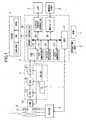
- FIG. 1is a block diagram of a system configuration of a digital camera as an example of the imaging device.
- the digital cameracomprises an optical system 1, an analog front end 2, a signal processor 3, an SDRAM 4, an LCD 5, a memory card 6, an ROM 7, and an operation unit 8, and a driver 9.
- the optical system 1includes a lens group 11, an aperture diaphragm 12, a shutter 13, and an image sensor 14.
- the analog front end 2includes a timing generator (TG) 21, a coupled double sampling (CDS) circuit 22, an analog gain control (AGC) circuit 23, and an A/D converter 24.
- the signal processor 3includes a CPU 21 as a controller, a CCD interface (I/F) 32, a memory controller 33, a YUV converter 34, a resize processor 35, a display output controller 36, a data compressor 37, and a media interface (I/F) 38.
- the optical system 1can include an ND (neutral density) filter.
- the image sensorcan be a CCD or a CMOS. With use of a CMOS, the analog front end 2 becomes unnecessary as an external circuit since it is generally incorporated in the CMOS.
- the CDS circuit 22removes noises from output signals of the image sensor, and the AGC circuit 23 amplifies the signals when needed.
- the A/D converter 24converts analog image signals to digital image data.
- the timing generator 21generates drive timing signals to the image sensor 14 and the elements of the analog front end 2.
- the CPU 31is connected to the CCD I/F 32, memory controller 33, YUV converter 34, resize processor 35, display output controller 36, data compressor 37 and media I/F 38 to perform data communication with them and control them.
- the memory controller 33is connected to the SDRAM 4, the display output controller is connected to the LCD 5, and the media I/F 38 is connected to the memory card 6.
- the CPU 31is connected to the ROM 7 storing operation programs and the operation unit 8 having buttons and switches with which data are input.
- the CPU 31also controls the driver 9 for the lens group 11, aperture diaphragm 12, and shutter 13.
- FIG. 2is a flowchart for brightness-based image synthesis processing of the digital camera in FIG. 1 including digital clamp with a black level variation taken into account by way of example.
- This image synthesisis executed by the CPU 31 of the signal processor 3.
- RAW imagesare properly subjected to digital clamp by adjusting a digital clamp amount in accordance with the number of synthesized images, ambient temperature, and photographic settings. Thereby, the black level of a synthesized image can be appropriately corrected.
- RAW imagesare assumed to be captured continuously in time series in the same composition under the same exposure and photographic condition including ISO sensitivity by the digital camera on a tripod.
- the imagescan include a moving subject.
- step S101ambient temperature is measured with a not-shown temperature sensor of the digital camera and the measured temperature is maintained.
- step S102data on photographic condition as exposure and sensitivity are acquired and maintained.
- step S103a first RAW image as a reference image is acquired and then subsequent RAW images as comparison images are acquired in step S104 for the brightness-based image synthesis.
- step S106the number of RAW images synthesized is counted as a parameter for digital clamping.
- the black level of a synthesized imageis properly corrected by digital clamp to shift the brightness of image data.
- Weighted average methodcan be added to the brightness-based image synthesis so as not to conduct pixel replacement for the same subject. In this case the range of weighted average needs to be determined by parameters.
- a noise distribution in a synthesized imagecan be decreased by reducing noises in the reference and comparison images used for the synthesis but a noise distribution cannot be eliminated and remains even at smaller absolute values. Therefore, the larger the number of images synthesized is, the more conspicuous the misadjustment and unevenness of the black level becomes. Further, each of RAW images to be synthesized can be subjected to dark frame subtraction, however, a noise distribution cannot be eliminated either and noise reduction is thus not sufficiently effective.
- step S107the synthesized image in step S105 is subjected to digital clamp.
- the black levels of the first to N-th RAW imagesare different depending on ambient temperature, photographic condition such as ISO sensitivity, exposure time, white balance, amount of peripheral light, the number of images synthesized N, and coordinates in a frame.
- an enormous amount of parameters and tables of combinations of calculationsare needed for digital clamp.
- a minimal necessary amount of calculationsis performed with the characteristics of black level obtained by experiment and measurement (as later described) taken into account.
- the black leveldoes not change till about ambient temperature 0 degree to 20 degrees C, but does change over 20 degrees C depending on exposure time. Thus, over the temperature 20 degrees C, omitting calculations relative to the ambient temperature makes it possible to greatly reduce the amount of parameters and tables of calculations although the effect of black level correction may be slightly decreased in high temperature portions depending on photographic condition.
- Sensitivity such as ISO sensitivityis approximately proportional to the black level. That is, if ISO sensitivity is doubled relative to a gain of the image sensor, random noise is approximately doubled accordingly.
- By using pre-stored data on the black level in association with the ISO sensitivityit is possible to accurately calculate the black level by a simple operation.
- the black levelis constant in image center areas irrespective of the amount of exposure time.
- the black leveltends to increase in proportion to the amount of exposure time probably because thermal noise distribution in frames is not even.
- black level data at each coordinate of a frame according to exposure timeare stored in a memory. The digital clamp is performed using this data in accordance with ISO sensitivity only and ambient temperature data is not used for the calculation.
- the black level data to be stored in the memoryare values of each point of a frame of a first image at each exposure time and the coefficients (A, B).
- the coordinates in a frameare ideally every pixel, however, it can be thinned with memory capacity taken into consideration.
- step S107a found digital clamp amount is subtracted from the synthesized image in the digital clamp process to output an obtained image to the SDRAM 4 via the memory controller 33 of the signal processor 3 or to the LCD 5 via the display output controller 36. Then, if there is a next image to be synthesized in step S108, the flow returns to step S105 and the above steps are repeated.
- This flowcan apply to image synthesis by replacing pixels with pixels with a lower brightness value.
- the maximal value of a noise distributionis set to a threshold, and brightness-based image synthesis is conducted only to the pixels with outputs equal to or over or below the threshold.
- FIG. 4shows the results of experiment in which RAW images are repeatedly subjected to the brightness-based image synthesis with a digital camera in a shaded state by way of example.
- a digital camera, RICOH GR DIGITAL IV manufactured by RICOH Co. Ltd.is used at ISO 400, exposure time 15 seconds, and F-value 9.0.
- the mean values of the black level of a center area of 50 by 50 pixels in a frame of 3,672 by 2,748 pixelsare plotted.
- a first imageexerts a black level of about 5 [LSB] in full scale, 12-bit equivalent, and the black level increases as the number of images increases and that of a 100 th image is near 30 [LSB].
- Such a high black levelis visually recognizable as grayish black.
- a night scenefor example, a dark sky is represented in a magenta-like color.
- data on a variation in the black level in accordance with the number of images synthesizedare prepared and stored in the memory.
- the misadjustment of the black level as grayish blackcan be prevented by adjusting the digital clamp amount in line with the number of images synthesized.
- a variation in the black levelchanges depending on ambient temperature, exposure time, the coordinates of an image and the characteristics of the image sensor so that the digital clamp amount needs to be adjusted according to these factors in the digital clamp process.
- FIG. 5shows a variation in the black level due to ambient temperature when the digital camera, RICOH GR DIGITAL IV is used at ISO 400, exposure time 1 to 30 seconds, and F-value 9.0.
- the mean values of the black level of a center area of 50 by 50 pixels in the size 3,672 by 2,748 pixels of a 1 st imageare plotted.
- the black leveltends to be higher than under normal-temperature environment because of an increase in dark currents, and how high the black level will be also differs depending on the amount of exposure time. For instance, at exposure time 1.0 second, the black level does not change from a low to high temperature. Meanwhile, at exposure time 30 seconds, the black level worsens conspicuously at high temperatures.
- FIG. 6shows a variation in the black level by exposure time when the digital camera, RICOH GR DIGITAL IV is used at ISO 100 to 3,200, exposure time 1 to 30 seconds, and F-value 9.0.
- the mean values of the black level of a center area of 50 by 50 pixels in the size of 3,672 by 2,748 pixels of a 1 st image at ambient temperature 25 degrees Care plotted. As apparent from the graph, the black level is correlated with exposure time and approximately proportional to ISO sensitivity.
- FIG. 7shows differences in the black level at different coordinates in an image frame when the digital camera, RICOH GR DIGITAL IV is used under normal ambient temperature of 25 degree C at ISO 100 to 400, exposure time 1 to 30 seconds, and F-value 9.0.
- the mean values of the black levels of a center area and a top left area of 50 by 50 pixels in the size of 3,672 by 2,748 pixels of a 1 st imageare plotted.
- the characteristics of the black level of the center areaare plotted by a solid line and those of the top left area are plotted by a broken line.
- the black leveldoes not change much while in the top left area the black level increases in proportion to the amount of exposure time.
- the black level of the center areais about 6 [LSB] while that of the top left area is about 67 [LSB], for example.
- FIG. 8shows a variation in the black level in accordance with the number of images synthesized as in FIG. 4 when the digital camera, RICOH GR DIGITAL IV is used at ISO 400, exposure time 15 seconds, and F-value 9.0.
- the mean values of the black levels of a center area and a top left area of 50 by 50 pixels in the size of 3,672 by 2,748 pixels of a 1 st image at normal ambient temperature of 25 degrees Care plotted.
- the black level of a first imageis set as a reference (100%) in FIG. 8 , the black level differently varies between the image center area and top left area.
- the digital clamp amountneeds to be calculated differently depending on the position in a frame.
- FIG. 9shows an example of image data captured with a digital camera in a shaded state. Note that the image data is tone-adjusted for the sake of clearly showing black unevenness. FIG. 9 clearly shows unevenness in the black level of an image frame. With use of a CCD solid image sensor as the image sensor 14, the black level unevenness is very noticeable because thermal noise distribution is uneven in a frame due to heat from amplifiers and peripheral circuits located in the area corresponding to the image top left area. Accordingly, different parameters need to be used for the digital clamp processing.
Landscapes
- Engineering & Computer Science (AREA)
- Theoretical Computer Science (AREA)
- Physics & Mathematics (AREA)
- General Physics & Mathematics (AREA)
- Computing Systems (AREA)
- Multimedia (AREA)
- Signal Processing (AREA)
- Studio Devices (AREA)
Description
- The present invention relates to an image processing of an imaging device such as a still digital camera with an image sensor, in particular, to an imaging device with an image synthesis function and an image processing method for image synthesis.
- A digital camera having an image synthesis function based on brightness is known. Such an image synthesis is to continuously shoot images in time series in the same composition under the same exposure, compare pixel output values of the same coordinates of a reference image and a comparison image, and synthesize the images while replacing the pixels of the reference image with the pixels of the comparison image with a higher output value or a lower output value. By this technique, for example, in photographing night scene, images of star tracks in a background with proper exposure can be captured. Digital cameras with such brightness-based image synthesis function are already available.
- Conventionally, for brightness-based image synthesis continuous images are generated with a camera and the images are synthesized by image processing software with a personal computer after shooting. Therefore, a user cannot generate synthesized images at the time of photographing. By use of a digital camera having image synthesis function, a user can check synthesized images during shooting.
- Further, for image synthesis with a personal computer, used image data are, for example, JPEG images with noise reduced and compressed when needed, therefore, the quality of the image data may not be good enough for image synthesis depending on photographic setting. Meanwhile, a digital camera can synthesize RAW images so that it can capture minute stars in colors which are likely to be considered as noise in a single frame, and improve image quality by averaging random noises in synthesizing process, which is not feasible by general image processing.
- Meanwhile, there is a problem in the synthesis of RAW images with the occurrence of noises from which the JPEG images are free because RAW images are raw output data from an image sensor not subjected to image processing. Due to shot noises or random noises, even image data of the same subject captured at the same setting cannot be the same output and is an output with probability distribution. While repeating a simple brightness-based image synthesis on pixels at the corresponding coordinates, the outputs gradually approach the maximal value of the distribution, resulting in generation of defective images such as over-exposure images or magenta-like images. This problem does not occur with JPEG images subjected to a digital clamp or noise reduction.
- Japanese Patent No.
4243084 2010-34845 Reference 1 discloses an imaging device to adjust clamping to RAW images in accordance with parameters for photographic conditions so as to reduce a variation in black level. It generates clamp signals properly in accordance with exposure data or temperature data in long exposure shooting or under a high ambient temperature.Reference 2 discloses a technique to tentatively increase an OB signal defining the black level in clamp processing to stabilize the black level, thereby preventing degradation in image quality due to a variation in the black level. However, the techniques in the two references cannot deal with variation or unevenness in the black level caused by brightness-based image synthesis of RAW images. - As described above, in synthesizing RAW images with an imaging device such as a digital camera having a brightness-based image synthesis function, a variation, unevenness or misadjustment in the black level may occur in accordance with a photographic condition under which RAW images are captured, an ambient condition, or a synthesis condition such as the number of images synthesized.
JP 2003 163839A JP 2010 187250 A - The present invention aims to provide an imaging device and an image processing method which can properly deal with a variation in black level in accordance with the number of images synthesized in brightness-based image synthesis of RAW images to effectively prevent degradation in the quality of synthesized images.
- The present invention is defined by the appended claims.
- Features, embodiments, and advantages of the present invention will become apparent from the following detailed description with reference to the accompanying drawings:
FIG. 1 is a block diagram of the essential part of a digital camera as an example of an imaging device according to one embodiment;FIG. 2 is a flowchart for brightness-based image synthesis including digital clamp processing of the digital camera inFIG. 1 in accordance with the number of images synthesized by way of example;FIG. 3 is a graph showing a noise distribution relative to signed differential values of a reference image and a comparison image by way of example;FIG. 4 is a graph showing a variation in black level relative to the number of images synthesized when RAW images are repeatedly subjected to a simple brightness-based image synthesis with a related art digital camera in an optically shielded state by way of example;FIG. 5 is a graph showing differences in the black level of images captured with the shielded digital camera inFIG. 4 in accordance with ambient temperature and exposure time by way of example;FIG. 6 is a graph showing differences in the black level of images captured with the shielded digital camera inFIG. 4 in accordance with sensitivity and exposure time by way of example;FIG. 7 is a graph showing differences in the black level of images at different coordinates captured with the shielded digital camera inFIG. 4 in accordance with sensitivity and exposure time by way of example;FIG. 8 is a graph showing a variation in the black level of images at different coordinates in accordance with the number of images synthesized by way of example; andFIG. 9 shows an image with unevenness in black level distribution generated using RAW images by brightness-based image synthesis of a related art digital camera when optically shielded.- Hereinafter, an imaging device and an image processing method according to an embodiment of the present invention will be described in detail with reference to the accompanying drawings. Wherever possible, the same reference numbers will be used throughout the drawings to refer to the same or like parts.
- First, brightness-based image synthesis is described. By the brightness-based image synthesis in which the pixel outputs at the same coordinates of multiple images are compared to replace the pixels with the ones with a higher or lower brightness, an imaging device can easily generate an image of star tracks, for example, even dark or thin color stars, which is not feasible by a silver-salt film camera. However, since RAW images are used, simple comparison of the pixel output values for pixel replacement causes increases in the total output level of an image due to shot noises or random noises. This results in increasing the black level and adding an offset to the output, thereby generating a magenta tone image.
- In view of this, the imaging device according to one embodiment is configured to store data on the number of RAW images synthesized, and a variation distribution in the black level of a synthesized image relative to photographic conditions or ambient conditions, and perform digital clamp to remove offset components of a synthesized image in accordance with the data. Thereby, it can more properly generate synthesized images in high quality using RAW images than using JPEG images, with noises taken into consideration.
FIG. 1 is a block diagram of a system configuration of a digital camera as an example of the imaging device. The digital camera comprises anoptical system 1, ananalog front end 2, asignal processor 3, anSDRAM 4, anLCD 5, amemory card 6, an ROM 7, and anoperation unit 8, and adriver 9.- The
optical system 1 includes alens group 11, anaperture diaphragm 12, ashutter 13, and animage sensor 14. Theanalog front end 2 includes a timing generator (TG) 21, a coupled double sampling (CDS)circuit 22, an analog gain control (AGC)circuit 23, and an A/D converter 24. Thesignal processor 3 includes aCPU 21 as a controller, a CCD interface (I/F) 32, amemory controller 33, aYUV converter 34, a resizeprocessor 35, adisplay output controller 36, adata compressor 37, and a media interface (I/F) 38. - The
optical system 1 can include an ND (neutral density) filter. The image sensor can be a CCD or a CMOS. With use of a CMOS, theanalog front end 2 becomes unnecessary as an external circuit since it is generally incorporated in the CMOS. - The
CDS circuit 22 removes noises from output signals of the image sensor, and theAGC circuit 23 amplifies the signals when needed. The A/D converter 24 converts analog image signals to digital image data. Thetiming generator 21 generates drive timing signals to theimage sensor 14 and the elements of theanalog front end 2. - The
CPU 31 is connected to the CCD I/F 32,memory controller 33,YUV converter 34, resizeprocessor 35,display output controller 36,data compressor 37 and media I/F 38 to perform data communication with them and control them. Thememory controller 33 is connected to theSDRAM 4, the display output controller is connected to theLCD 5, and the media I/F 38 is connected to thememory card 6. Further, theCPU 31 is connected to the ROM 7 storing operation programs and theoperation unit 8 having buttons and switches with which data are input. TheCPU 31 also controls thedriver 9 for thelens group 11,aperture diaphragm 12, andshutter 13. FIG. 2 is a flowchart for brightness-based image synthesis processing of the digital camera inFIG. 1 including digital clamp with a black level variation taken into account by way of example. This image synthesis is executed by theCPU 31 of thesignal processor 3. In the brightness-based image synthesis according to the present embodiment RAW images are properly subjected to digital clamp by adjusting a digital clamp amount in accordance with the number of synthesized images, ambient temperature, and photographic settings. Thereby, the black level of a synthesized image can be appropriately corrected.- In
FIG. 2 RAW images are assumed to be captured continuously in time series in the same composition under the same exposure and photographic condition including ISO sensitivity by the digital camera on a tripod. The images can include a moving subject. - In step S101 ambient temperature is measured with a not-shown temperature sensor of the digital camera and the measured temperature is maintained. In step S102 data on photographic condition as exposure and sensitivity are acquired and maintained. In step S103 a first RAW image as a reference image is acquired and then subsequent RAW images as comparison images are acquired in step S104 for the brightness-based image synthesis. In step S105 first to N-th (N = 2 or more) RAW images are subjected to brightness-based image synthesis repeatedly to generate a synthesized image while replacing the pixels of the reference image with the pixels of the comparison images with a higher brightness value. In step S106 the number of RAW images synthesized is counted as a parameter for digital clamping.
- To prevent misadjustment and unevenness in the black level due to noises, in the present embodiment the black level of a synthesized image is properly corrected by digital clamp to shift the brightness of image data. Weighted average method can be added to the brightness-based image synthesis so as not to conduct pixel replacement for the same subject. In this case the range of weighted average needs to be determined by parameters. However, there will be a tradeoff between the accuracy of brightness-based image synthesis and misadjustment and unevenness in the black level. That is, without the addition of the weighted average, the black level of a synthesized image has to be properly corrected.
- For a simple brightness-based image synthesis, a noise distribution in a synthesized image can be decreased by reducing noises in the reference and comparison images used for the synthesis but a noise distribution cannot be eliminated and remains even at smaller absolute values. Therefore, the larger the number of images synthesized is, the more conspicuous the misadjustment and unevenness of the black level becomes. Further, each of RAW images to be synthesized can be subjected to dark frame subtraction, however, a noise distribution cannot be eliminated either and noise reduction is thus not sufficiently effective.
- Returning to the flowchart, in step S107 the synthesized image in step S105 is subjected to digital clamp. The black levels of the first to N-th RAW images are different depending on ambient temperature, photographic condition such as ISO sensitivity, exposure time, white balance, amount of peripheral light, the number of images synthesized N, and coordinates in a frame. Thus, an enormous amount of parameters and tables of combinations of calculations are needed for digital clamp. Herein, a minimal necessary amount of calculations is performed with the characteristics of black level obtained by experiment and measurement (as later described) taken into account.
- The black level does not change till about
ambient temperature 0 degree to 20 degrees C, but does change over 20 degrees C depending on exposure time. Thus, over thetemperature 20 degrees C, omitting calculations relative to the ambient temperature makes it possible to greatly reduce the amount of parameters and tables of calculations although the effect of black level correction may be slightly decreased in high temperature portions depending on photographic condition. - Sensitivity such as ISO sensitivity is approximately proportional to the black level. That is, if ISO sensitivity is doubled relative to a gain of the image sensor, random noise is approximately doubled accordingly. By using pre-stored data on the black level in association with the ISO sensitivity, it is possible to accurately calculate the black level by a simple operation.
- Regarding the exposure time, the black level is constant in image center areas irrespective of the amount of exposure time. However, in image top left portions, for example, the black level tends to increase in proportion to the amount of exposure time probably because thermal noise distribution in frames is not even. In the present embodiment black level data at each coordinate of a frame according to exposure time are stored in a memory. The digital clamp is performed using this data in accordance with ISO sensitivity only and ambient temperature data is not used for the calculation.
- Further, with regard to the number of images synthesized, the black level also changes at different coordinates in a frame but can be approximated by logarithm function. That is, the black level L (N) of the N-th image is expressed by the following equation:

- The black level data to be stored in the memory are values of each point of a frame of a first image at each exposure time and the coefficients (A, B). The coordinates in a frame are ideally every pixel, however, it can be thinned with memory capacity taken into consideration.
- In step S107 a found digital clamp amount is subtracted from the synthesized image in the digital clamp process to output an obtained image to the
SDRAM 4 via thememory controller 33 of thesignal processor 3 or to theLCD 5 via thedisplay output controller 36. Then, if there is a next image to be synthesized in step S108, the flow returns to step S105 and the above steps are repeated. This flow can apply to image synthesis by replacing pixels with pixels with a lower brightness value. - Next, a problem in a simple brightness-based image synthesis without the use of the present invention is described. In general the pixel outputs of RAW images of the same subject captured under the same photographic condition are not the same due to noises. By a simple brightness-based image synthesis, the outputs gradually approach the maximal value of a noise distribution as shown in
FIG. 3 . InFIG. 3 a normal distribution σ2 = 5 is assumed as a noise distribution model. - In view of this, according to the present embodiment the maximal value of a noise distribution is set to a threshold, and brightness-based image synthesis is conducted only to the pixels with outputs equal to or over or below the threshold.
FIG. 4 shows the results of experiment in which RAW images are repeatedly subjected to the brightness-based image synthesis with a digital camera in a shaded state by way of example. A digital camera, RICOH GR DIGITAL IV manufactured by RICOH Co. Ltd. is used atISO 400,exposure time 15 seconds, and F-value 9.0. InFIG. 4 the mean values of the black level of a center area of 50 by 50 pixels in a frame of 3,672 by 2,748 pixels are plotted. As seen from the drawing, a first image exerts a black level of about 5 [LSB] in full scale, 12-bit equivalent, and the black level increases as the number of images increases and that of a 100th image is near 30 [LSB]. Such a high black level is visually recognizable as grayish black. In a night scene, for example, a dark sky is represented in a magenta-like color.- In view of this, in the present embodiment data on a variation in the black level in accordance with the number of images synthesized are prepared and stored in the memory. Thus, the misadjustment of the black level as grayish black can be prevented by adjusting the digital clamp amount in line with the number of images synthesized. Further, a variation in the black level changes depending on ambient temperature, exposure time, the coordinates of an image and the characteristics of the image sensor so that the digital clamp amount needs to be adjusted according to these factors in the digital clamp process.
FIG. 5 shows a variation in the black level due to ambient temperature when the digital camera, RICOH GR DIGITAL IV is used atISO 400,exposure time 1 to 30 seconds, and F-value 9.0. The mean values of the black level of a center area of 50 by 50 pixels in the size 3,672 by 2,748 pixels of a 1st image are plotted.- It is seen from the graph that under high-temperature environment the black level tends to be higher than under normal-temperature environment because of an increase in dark currents, and how high the black level will be also differs depending on the amount of exposure time. For instance, at exposure time 1.0 second, the black level does not change from a low to high temperature. Meanwhile, at
exposure time 30 seconds, the black level worsens conspicuously at high temperatures. FIG. 6 shows a variation in the black level by exposure time when the digital camera, RICOH GR DIGITAL IV is used atISO 100 to 3,200,exposure time 1 to 30 seconds, and F-value 9.0. The mean values of the black level of a center area of 50 by 50 pixels in the size of 3,672 by 2,748 pixels of a 1st image atambient temperature 25 degrees C are plotted. As apparent from the graph, the black level is correlated with exposure time and approximately proportional to ISO sensitivity.FIG. 7 shows differences in the black level at different coordinates in an image frame when the digital camera, RICOH GR DIGITAL IV is used under normal ambient temperature of 25 degree C atISO 100 to 400,exposure time 1 to 30 seconds, and F-value 9.0. The mean values of the black levels of a center area and a top left area of 50 by 50 pixels in the size of 3,672 by 2,748 pixels of a 1st image are plotted. The characteristics of the black level of the center area are plotted by a solid line and those of the top left area are plotted by a broken line. In the central area the black level does not change much while in the top left area the black level increases in proportion to the amount of exposure time. Specifically, atISO 400 and exposure time 30 [sec] the black level of the center area is about 6 [LSB] while that of the top left area is about 67 [LSB], for example.FIG. 8 shows a variation in the black level in accordance with the number of images synthesized as inFIG. 4 when the digital camera, RICOH GR DIGITAL IV is used atISO 400,exposure time 15 seconds, and F-value 9.0. The mean values of the black levels of a center area and a top left area of 50 by 50 pixels in the size of 3,672 by 2,748 pixels of a 1st image at normal ambient temperature of 25 degrees C are plotted.- When the black level of a first image is set as a reference (100%) in
FIG. 8 , the black level differently varies between the image center area and top left area. Thus, the digital clamp amount needs to be calculated differently depending on the position in a frame. FIG. 9 shows an example of image data captured with a digital camera in a shaded state. Note that the image data is tone-adjusted for the sake of clearly showing black unevenness.FIG. 9 clearly shows unevenness in the black level of an image frame. With use of a CCD solid image sensor as theimage sensor 14, the black level unevenness is very noticeable because thermal noise distribution is uneven in a frame due to heat from amplifiers and peripheral circuits located in the area corresponding to the image top left area. Accordingly, different parameters need to be used for the digital clamp processing.- Although the present invention has been described in terms of exemplary embodiments, it is not limited thereto. It should be appreciated that variations or modifications may be made in the embodiments described by persons skilled in the art without departing from the scope of the present invention as defined by the following claims.

Claims (8)
- An imaging device comprising:an image sensor (14) to convert an optical image of a subject into an electric signal;an image processor to generate a RAW image according to the electric signal;an image synthesizer to perform brightness based synthesis, pixel-by-pixel, of RAW images comprising a first image and one or more subsequent images generated by the image processor in the same composition under the same exposure condition by repeatedly replacing pixels of the first image with pixels of the one or more subsequent images at the same coordinates with a higher brightness value to obtain a synthesized image; andcharacterised bya digital clamp processor to perform a digital black-level clamp of a digital black-level clamp amount to remove black-level offset component from a synthesized image obtained by the image synthesizer, said digital black-level clamp being performed based on pre-stored black-level data, wherein the digital black-level clamp amount is subtracted from the synthesized image; anda digital clamp controller to control the digital black-level clamp amount of the digital clamp processor on the basis of the number of images synthesized by the image synthesizer.
- An imaging device comprising:an image sensor (14) to convert an optical image of a subject into an electric signal;an image processor to generate a RAW image according to the electric signal;an image synthesizer to perform brightness based synthesis, pixel-by-pixel, of RAW images comprising a first image and one or more subsequent images generated by the image processor in the same composition under the same exposure condition by repeatedly replacing pixels of the first image with pixels of the one or more subsequent images at the same coordinates with a lower brightness value to obtain a synthesized image; andcharacterised bya digital clamp processor to perform a digital black-level clamp of a digital black-level clamp amount to remove black-level offset component from a synthesized image obtained by the image synthesizer, said digital black-level clamp being performed based on pre-stored black-level data, wherein the digital black-level clamp amount is subtracted from the synthesized image; anda digital clamp controller to control the digital black-level clamp amount of the digital clamp processor on the basis of the number of images synthesized by the image synthesizer.
- The imaging device according to either claim 1 or 2, wherein
the digital clamp controller includes a first controller to control the digital clamp amount in accordance with at least one of sensitivity, white balance, exposure time, a correction amount of peripheral light amount, and ambient temperature. - An imaging device according to any one of claims 1 to 3, wherein
the digital clamp controller includes a further controller to control the digital clamp amount in accordance with the coordinates of the synthesized image. - An image processing method, comprising the steps of:converting an optical image of a subject into an electric signal;generating a RAW image according to the electric signal;performing brightness based synthesis, pixel-by-pixel, of RAW images comprising a first image and one or more subsequent images generated in the same composition under the same condition by repeatedly replacing pixels of the first image with pixels of the one or more subsequent images at the same coordinates with a higher brightness value to obtain a synthesized image;performing a digital black-level clamp at a digital black-level clamp amount to remove black-level offset component from a synthesized image obtained in the synthesizing step, said digital black-level clamp being performed based on pre-stored black-level data, wherein the digital black-level clamp amount is subtracted from the synthesized image; andcontrolling the digital black-level clamp amount on the basis of the number of images synthesized in the synthesizing step.
- An image processing method, comprising the steps of:converting an optical image of a subject into an electric signal;generating a RAW image according to the electric signal;performing brightness based synthesis, pixel-by-pixel, of RAW images comprising a first image and one or more subsequent images generated in the same composition under the same condition by repeatedly replacing pixels of the first image with pixels of the one or more subsequent images at the same coordinates with a lower brightness value to obtain a synthesized image;performing a digital black-level clamp at a digital black-level clamp amount to remove black-level offset component from a synthesized image obtained in the synthesizing step, said digital black-level clamp being performed based on pre-stored black-level data, wherein the digital black-level clamp amount is subtracted from the synthesized image; andcontrolling the digital black-level clamp amount on the basis of the number of images synthesized in the synthesizing step.
- The image processing method according to either claim 5 or 6, wherein
the digital clamp controlling step comprises controlling the digital clamp amount in accordance with at least one of sensitivity, white balance, exposure time, a correction amount of peripheral light amount, and ambient temperature. - The image processing method according to any one of claims 5 to 7, further comprising the step of
controlling at least either the change amount or the digital clamp amount in accordance with the coordinates of the synthesized image.
Applications Claiming Priority (2)
| Application Number | Priority Date | Filing Date | Title |
|---|---|---|---|
| JP2012097204 | 2012-04-20 | ||
| PCT/JP2013/062151WO2013157662A1 (en) | 2012-04-20 | 2013-04-18 | Imaging device and image processing method |
Publications (3)
| Publication Number | Publication Date |
|---|---|
| EP2839634A1 EP2839634A1 (en) | 2015-02-25 |
| EP2839634A4 EP2839634A4 (en) | 2015-04-22 |
| EP2839634B1true EP2839634B1 (en) | 2018-05-30 |
Family
ID=49383602
Family Applications (1)
| Application Number | Title | Priority Date | Filing Date |
|---|---|---|---|
| EP13778083.9ANot-in-forceEP2839634B1 (en) | 2012-04-20 | 2013-04-18 | Imaging device and image processing method |
Country Status (5)
| Country | Link |
|---|---|
| US (1) | US9444979B2 (en) |
| EP (1) | EP2839634B1 (en) |
| JP (1) | JP5954623B2 (en) |
| CN (1) | CN104221364B (en) |
| WO (1) | WO2013157662A1 (en) |
Families Citing this family (9)
| Publication number | Priority date | Publication date | Assignee | Title |
|---|---|---|---|---|
| WO2016026455A1 (en)* | 2014-08-22 | 2016-02-25 | 努比亚技术有限公司 | Method and device for automatically optimizing star trail photography result |
| CN105072350B (en) | 2015-06-30 | 2019-09-27 | 华为技术有限公司 | Method and device for taking pictures |
| CN106341590B (en)* | 2015-10-10 | 2019-05-21 | 北京智谷睿拓技术服务有限公司 | Image Acquisition control method and device, image capture device |
| JP6736279B2 (en) | 2015-10-14 | 2020-08-05 | オリンパス株式会社 | Imaging device, image processing device, and image processing method |
| US20190114814A1 (en)* | 2017-10-18 | 2019-04-18 | Yagerbomb Media Pvt. Ltd. | Method and system for customization of pictures on real time dynamic basis |
| CN108111785B (en)* | 2017-12-28 | 2020-05-15 | Oppo广东移动通信有限公司 | Image processing method and device, computer readable storage medium and computer device |
| CN111147693B (en)* | 2019-04-28 | 2022-04-29 | 广东小天才科技有限公司 | Noise reduction method and device for full-size photographed image |
| JP7306089B2 (en) | 2019-06-17 | 2023-07-11 | 株式会社リコー | Image processing system, imaging system, image processing device, imaging device, and program |
| CN114928682A (en)* | 2022-04-08 | 2022-08-19 | 湖北工程学院 | High-temperature metal piece surface pattern shooting system and method |
Family Cites Families (21)
| Publication number | Priority date | Publication date | Assignee | Title |
|---|---|---|---|---|
| JPH11313252A (en)* | 1998-04-30 | 1999-11-09 | Canon Inc | Digital camera device, image processing method, storage medium |
| JP4148586B2 (en)* | 1999-03-08 | 2008-09-10 | カシオ計算機株式会社 | Image synthesizer |
| US7050098B2 (en)* | 2001-03-29 | 2006-05-23 | Canon Kabushiki Kaisha | Signal processing apparatus and method, and image sensing apparatus having a plurality of image sensing regions per image frame |
| JP2003163839A (en) | 2001-09-12 | 2003-06-06 | Ricoh Co Ltd | Image input device |
| JP4243084B2 (en)* | 2002-09-27 | 2009-03-25 | 富士フイルム株式会社 | Solid-state imaging device and signal processing method thereof |
| JP4218357B2 (en)* | 2003-01-31 | 2009-02-04 | セイコーエプソン株式会社 | Digital clamp circuit and digital clamp processing method |
| JP4082318B2 (en)* | 2003-09-04 | 2008-04-30 | カシオ計算機株式会社 | Imaging apparatus, image processing method, and program |
| JP4379230B2 (en)* | 2004-07-07 | 2009-12-09 | ソニー株式会社 | Solid-state image sensor device and signal processing method |
| US7701493B2 (en)* | 2005-02-28 | 2010-04-20 | Micron Technology, Inc. | Imager row-wise noise correction |
| JP2007158663A (en)* | 2005-12-05 | 2007-06-21 | Ricoh Co Ltd | Analog image signal offset adjustment method |
| US7760258B2 (en)* | 2007-03-07 | 2010-07-20 | Altasens, Inc. | Apparatus and method for stabilizing image sensor black level |
| JP5034610B2 (en)* | 2007-03-30 | 2012-09-26 | ソニー株式会社 | Solid-state imaging device, signal processing method for solid-state imaging device, and imaging device |
| JP4980131B2 (en)* | 2007-05-01 | 2012-07-18 | 富士フイルム株式会社 | Noise reduction apparatus and method, and program |
| JP2009017078A (en) | 2007-07-03 | 2009-01-22 | Fujifilm Corp | Digital still camera and operation control method thereof |
| JP2009276956A (en)* | 2008-05-14 | 2009-11-26 | Fujifilm Corp | Image processing apparatus and method, and program |
| JP5155763B2 (en) | 2008-07-29 | 2013-03-06 | 富士フイルム株式会社 | Imaging apparatus and imaging control method |
| JP5206466B2 (en) | 2009-02-13 | 2013-06-12 | 富士通株式会社 | Image correction apparatus, image correction program, and image photographing apparatus |
| CN102158684A (en)* | 2010-02-12 | 2011-08-17 | 王炳立 | Self-adapting scene image auxiliary system with image enhancement function |
| JP2012065115A (en)* | 2010-09-15 | 2012-03-29 | Ricoh Co Ltd | Image processing apparatus and method |
| JP5652649B2 (en) | 2010-10-07 | 2015-01-14 | 株式会社リコー | Image processing apparatus, image processing method, and image processing program |
| JP5861924B2 (en) | 2011-12-26 | 2016-02-16 | 株式会社リコー | Imaging device |
- 2012
- 2012-05-31JPJP2012124078Apatent/JP5954623B2/ennot_activeExpired - Fee Related
- 2013
- 2013-04-18WOPCT/JP2013/062151patent/WO2013157662A1/enactiveApplication Filing
- 2013-04-18USUS14/380,832patent/US9444979B2/enactiveActive
- 2013-04-18CNCN201380019588.9Apatent/CN104221364B/ennot_activeExpired - Fee Related
- 2013-04-18EPEP13778083.9Apatent/EP2839634B1/ennot_activeNot-in-force
Non-Patent Citations (1)
| Title |
|---|
| None* |
Also Published As
| Publication number | Publication date |
|---|---|
| CN104221364B (en) | 2018-06-22 |
| US9444979B2 (en) | 2016-09-13 |
| CN104221364A (en) | 2014-12-17 |
| WO2013157662A1 (en) | 2013-10-24 |
| EP2839634A4 (en) | 2015-04-22 |
| JP5954623B2 (en) | 2016-07-20 |
| EP2839634A1 (en) | 2015-02-25 |
| JP2013240029A (en) | 2013-11-28 |
| US20150042847A1 (en) | 2015-02-12 |
Similar Documents
| Publication | Publication Date | Title |
|---|---|---|
| EP2839634B1 (en) | Imaging device and image processing method | |
| US8405738B2 (en) | Image pickup apparatus and method of picking up image | |
| US11159740B2 (en) | Image capturing device and control method thereof and medium | |
| US9838625B2 (en) | Image processing apparatus and control method for image processing apparatus for controlling correction of a black level in a combined image signal | |
| JP2003204486A (en) | Imaging device | |
| KR20070035991A (en) | Imaging Apparatus, Exposure Control Apparatus, Method and Program | |
| JP4444218B2 (en) | Brightness correction apparatus for moving picture, control method thereof and control program thereof | |
| US20120162467A1 (en) | Image capture device | |
| US9113117B2 (en) | Image-taking apparatus and method for controlling the same | |
| US8155472B2 (en) | Image processing apparatus, camera, image processing program product and image processing method | |
| WO2016171087A1 (en) | Image processing device, image capturing apparatus, image processing method and image processing program | |
| JP2013135343A (en) | Imaging device | |
| US9191573B2 (en) | Image capturing apparatus for determining an exposure condition by calculating aphotmetric value for each object region and method of controlling the same | |
| JP2008085634A (en) | Imaging apparatus and image processing method | |
| JP5515795B2 (en) | Imaging apparatus and imaging method | |
| US10475162B2 (en) | Image processing device, method, and storage medium for gamma correction based on illuminance | |
| US20090015691A1 (en) | Image pickup apparatus and method for controlling the same | |
| JP6090565B2 (en) | Imaging apparatus, imaging method, and program | |
| JP2015100091A (en) | Image processing apparatus, imaging apparatus, image processing method, and program | |
| JP2023119719A (en) | Imaging apparatus and method for controlling the same | |
| JP6704611B2 (en) | Imaging device and imaging method | |
| US8625008B2 (en) | Image processing apparatus having luminance-type gamma correction circuit capable of changing nonlinear characteristic, and image processing method therefor | |
| JP2012205031A (en) | Image signal processing apparatus | |
| JP2006165937A (en) | Imaging device | |
| JP2009177669A (en) | Imaging device |
Legal Events
| Date | Code | Title | Description |
|---|---|---|---|
| PUAI | Public reference made under article 153(3) epc to a published international application that has entered the european phase | Free format text:ORIGINAL CODE: 0009012 | |
| 17P | Request for examination filed | Effective date:20140829 | |
| AK | Designated contracting states | Kind code of ref document:A1 Designated state(s):AL AT BE BG CH CY CZ DE DK EE ES FI FR GB GR HR HU IE IS IT LI LT LU LV MC MK MT NL NO PL PT RO RS SE SI SK SM TR | |
| AX | Request for extension of the european patent | Extension state:BA ME | |
| RA4 | Supplementary search report drawn up and despatched (corrected) | Effective date:20150320 | |
| RIC1 | Information provided on ipc code assigned before grant | Ipc:G06T 3/00 20060101ALI20150316BHEP Ipc:G06T 5/00 20060101ALI20150316BHEP Ipc:G06T 5/50 20060101ALI20150316BHEP Ipc:H04N 5/217 20110101ALI20150316BHEP Ipc:H04N 5/361 20110101ALI20150316BHEP Ipc:H04N 5/232 20060101ALI20150316BHEP Ipc:H04N 5/243 20060101AFI20150316BHEP | |
| DAX | Request for extension of the european patent (deleted) | ||
| STAA | Information on the status of an ep patent application or granted ep patent | Free format text:STATUS: EXAMINATION IS IN PROGRESS | |
| 17Q | First examination report despatched | Effective date:20170102 | |
| GRAP | Despatch of communication of intention to grant a patent | Free format text:ORIGINAL CODE: EPIDOSNIGR1 | |
| STAA | Information on the status of an ep patent application or granted ep patent | Free format text:STATUS: GRANT OF PATENT IS INTENDED | |
| RIN1 | Information on inventor provided before grant (corrected) | Inventor name:HOHJOH, DALSUKE | |
| INTG | Intention to grant announced | Effective date:20180124 | |
| GRAS | Grant fee paid | Free format text:ORIGINAL CODE: EPIDOSNIGR3 | |
| GRAA | (expected) grant | Free format text:ORIGINAL CODE: 0009210 | |
| STAA | Information on the status of an ep patent application or granted ep patent | Free format text:STATUS: THE PATENT HAS BEEN GRANTED | |
| AK | Designated contracting states | Kind code of ref document:B1 Designated state(s):AL AT BE BG CH CY CZ DE DK EE ES FI FR GB GR HR HU IE IS IT LI LT LU LV MC MK MT NL NO PL PT RO RS SE SI SK SM TR | |
| REG | Reference to a national code | Ref country code:GB Ref legal event code:FG4D | |
| REG | Reference to a national code | Ref country code:CH Ref legal event code:EP | |
| REG | Reference to a national code | Ref country code:AT Ref legal event code:REF Ref document number:1004828 Country of ref document:AT Kind code of ref document:T Effective date:20180615 | |
| REG | Reference to a national code | Ref country code:IE Ref legal event code:FG4D | |
| REG | Reference to a national code | Ref country code:DE Ref legal event code:R096 Ref document number:602013038248 Country of ref document:DE | |
| REG | Reference to a national code | Ref country code:NL Ref legal event code:MP Effective date:20180530 | |
| REG | Reference to a national code | Ref country code:LT Ref legal event code:MG4D | |
| PG25 | Lapsed in a contracting state [announced via postgrant information from national office to epo] | Ref country code:NO Free format text:LAPSE BECAUSE OF FAILURE TO SUBMIT A TRANSLATION OF THE DESCRIPTION OR TO PAY THE FEE WITHIN THE PRESCRIBED TIME-LIMIT Effective date:20180830 Ref country code:FI Free format text:LAPSE BECAUSE OF FAILURE TO SUBMIT A TRANSLATION OF THE DESCRIPTION OR TO PAY THE FEE WITHIN THE PRESCRIBED TIME-LIMIT Effective date:20180530 Ref country code:BG Free format text:LAPSE BECAUSE OF FAILURE TO SUBMIT A TRANSLATION OF THE DESCRIPTION OR TO PAY THE FEE WITHIN THE PRESCRIBED TIME-LIMIT Effective date:20180830 Ref country code:CY Free format text:LAPSE BECAUSE OF FAILURE TO SUBMIT A TRANSLATION OF THE DESCRIPTION OR TO PAY THE FEE WITHIN THE PRESCRIBED TIME-LIMIT Effective date:20180530 Ref country code:ES Free format text:LAPSE BECAUSE OF FAILURE TO SUBMIT A TRANSLATION OF THE DESCRIPTION OR TO PAY THE FEE WITHIN THE PRESCRIBED TIME-LIMIT Effective date:20180530 Ref country code:SE Free format text:LAPSE BECAUSE OF FAILURE TO SUBMIT A TRANSLATION OF THE DESCRIPTION OR TO PAY THE FEE WITHIN THE PRESCRIBED TIME-LIMIT Effective date:20180530 Ref country code:LT Free format text:LAPSE BECAUSE OF FAILURE TO SUBMIT A TRANSLATION OF THE DESCRIPTION OR TO PAY THE FEE WITHIN THE PRESCRIBED TIME-LIMIT Effective date:20180530 | |
| PG25 | Lapsed in a contracting state [announced via postgrant information from national office to epo] | Ref country code:LV Free format text:LAPSE BECAUSE OF FAILURE TO SUBMIT A TRANSLATION OF THE DESCRIPTION OR TO PAY THE FEE WITHIN THE PRESCRIBED TIME-LIMIT Effective date:20180530 Ref country code:HR Free format text:LAPSE BECAUSE OF FAILURE TO SUBMIT A TRANSLATION OF THE DESCRIPTION OR TO PAY THE FEE WITHIN THE PRESCRIBED TIME-LIMIT Effective date:20180530 Ref country code:GR Free format text:LAPSE BECAUSE OF FAILURE TO SUBMIT A TRANSLATION OF THE DESCRIPTION OR TO PAY THE FEE WITHIN THE PRESCRIBED TIME-LIMIT Effective date:20180831 Ref country code:RS Free format text:LAPSE BECAUSE OF FAILURE TO SUBMIT A TRANSLATION OF THE DESCRIPTION OR TO PAY THE FEE WITHIN THE PRESCRIBED TIME-LIMIT Effective date:20180530 | |
| REG | Reference to a national code | Ref country code:AT Ref legal event code:MK05 Ref document number:1004828 Country of ref document:AT Kind code of ref document:T Effective date:20180530 | |
| PG25 | Lapsed in a contracting state [announced via postgrant information from national office to epo] | Ref country code:NL Free format text:LAPSE BECAUSE OF FAILURE TO SUBMIT A TRANSLATION OF THE DESCRIPTION OR TO PAY THE FEE WITHIN THE PRESCRIBED TIME-LIMIT Effective date:20180530 | |
| PG25 | Lapsed in a contracting state [announced via postgrant information from national office to epo] | Ref country code:PL Free format text:LAPSE BECAUSE OF FAILURE TO SUBMIT A TRANSLATION OF THE DESCRIPTION OR TO PAY THE FEE WITHIN THE PRESCRIBED TIME-LIMIT Effective date:20180530 Ref country code:AT Free format text:LAPSE BECAUSE OF FAILURE TO SUBMIT A TRANSLATION OF THE DESCRIPTION OR TO PAY THE FEE WITHIN THE PRESCRIBED TIME-LIMIT Effective date:20180530 Ref country code:EE Free format text:LAPSE BECAUSE OF FAILURE TO SUBMIT A TRANSLATION OF THE DESCRIPTION OR TO PAY THE FEE WITHIN THE PRESCRIBED TIME-LIMIT Effective date:20180530 Ref country code:RO Free format text:LAPSE BECAUSE OF FAILURE TO SUBMIT A TRANSLATION OF THE DESCRIPTION OR TO PAY THE FEE WITHIN THE PRESCRIBED TIME-LIMIT Effective date:20180530 Ref country code:CZ Free format text:LAPSE BECAUSE OF FAILURE TO SUBMIT A TRANSLATION OF THE DESCRIPTION OR TO PAY THE FEE WITHIN THE PRESCRIBED TIME-LIMIT Effective date:20180530 Ref country code:SK Free format text:LAPSE BECAUSE OF FAILURE TO SUBMIT A TRANSLATION OF THE DESCRIPTION OR TO PAY THE FEE WITHIN THE PRESCRIBED TIME-LIMIT Effective date:20180530 Ref country code:DK Free format text:LAPSE BECAUSE OF FAILURE TO SUBMIT A TRANSLATION OF THE DESCRIPTION OR TO PAY THE FEE WITHIN THE PRESCRIBED TIME-LIMIT Effective date:20180530 | |
| PG25 | Lapsed in a contracting state [announced via postgrant information from national office to epo] | Ref country code:SM Free format text:LAPSE BECAUSE OF FAILURE TO SUBMIT A TRANSLATION OF THE DESCRIPTION OR TO PAY THE FEE WITHIN THE PRESCRIBED TIME-LIMIT Effective date:20180530 Ref country code:IT Free format text:LAPSE BECAUSE OF FAILURE TO SUBMIT A TRANSLATION OF THE DESCRIPTION OR TO PAY THE FEE WITHIN THE PRESCRIBED TIME-LIMIT Effective date:20180530 | |
| REG | Reference to a national code | Ref country code:DE Ref legal event code:R097 Ref document number:602013038248 Country of ref document:DE | |
| PLBE | No opposition filed within time limit | Free format text:ORIGINAL CODE: 0009261 | |
| STAA | Information on the status of an ep patent application or granted ep patent | Free format text:STATUS: NO OPPOSITION FILED WITHIN TIME LIMIT | |
| 26N | No opposition filed | Effective date:20190301 | |
| PG25 | Lapsed in a contracting state [announced via postgrant information from national office to epo] | Ref country code:SI Free format text:LAPSE BECAUSE OF FAILURE TO SUBMIT A TRANSLATION OF THE DESCRIPTION OR TO PAY THE FEE WITHIN THE PRESCRIBED TIME-LIMIT Effective date:20180530 | |
| PG25 | Lapsed in a contracting state [announced via postgrant information from national office to epo] | Ref country code:AL Free format text:LAPSE BECAUSE OF FAILURE TO SUBMIT A TRANSLATION OF THE DESCRIPTION OR TO PAY THE FEE WITHIN THE PRESCRIBED TIME-LIMIT Effective date:20180530 | |
| REG | Reference to a national code | Ref country code:CH Ref legal event code:PL | |
| REG | Reference to a national code | Ref country code:BE Ref legal event code:MM Effective date:20190430 | |
| PG25 | Lapsed in a contracting state [announced via postgrant information from national office to epo] | Ref country code:LU Free format text:LAPSE BECAUSE OF NON-PAYMENT OF DUE FEES Effective date:20190418 Ref country code:MC Free format text:LAPSE BECAUSE OF FAILURE TO SUBMIT A TRANSLATION OF THE DESCRIPTION OR TO PAY THE FEE WITHIN THE PRESCRIBED TIME-LIMIT Effective date:20180530 | |
| PG25 | Lapsed in a contracting state [announced via postgrant information from national office to epo] | Ref country code:CH Free format text:LAPSE BECAUSE OF NON-PAYMENT OF DUE FEES Effective date:20190430 Ref country code:LI Free format text:LAPSE BECAUSE OF NON-PAYMENT OF DUE FEES Effective date:20190430 | |
| PG25 | Lapsed in a contracting state [announced via postgrant information from national office to epo] | Ref country code:BE Free format text:LAPSE BECAUSE OF NON-PAYMENT OF DUE FEES Effective date:20190430 | |
| PG25 | Lapsed in a contracting state [announced via postgrant information from national office to epo] | Ref country code:TR Free format text:LAPSE BECAUSE OF FAILURE TO SUBMIT A TRANSLATION OF THE DESCRIPTION OR TO PAY THE FEE WITHIN THE PRESCRIBED TIME-LIMIT Effective date:20180530 | |
| PG25 | Lapsed in a contracting state [announced via postgrant information from national office to epo] | Ref country code:IE Free format text:LAPSE BECAUSE OF NON-PAYMENT OF DUE FEES Effective date:20190418 | |
| PG25 | Lapsed in a contracting state [announced via postgrant information from national office to epo] | Ref country code:PT Free format text:LAPSE BECAUSE OF FAILURE TO SUBMIT A TRANSLATION OF THE DESCRIPTION OR TO PAY THE FEE WITHIN THE PRESCRIBED TIME-LIMIT Effective date:20181001 | |
| PGFP | Annual fee paid to national office [announced via postgrant information from national office to epo] | Ref country code:DE Payment date:20200420 Year of fee payment:8 Ref country code:FR Payment date:20200420 Year of fee payment:8 | |
| PGFP | Annual fee paid to national office [announced via postgrant information from national office to epo] | Ref country code:GB Payment date:20200427 Year of fee payment:8 | |
| PG25 | Lapsed in a contracting state [announced via postgrant information from national office to epo] | Ref country code:IS Free format text:LAPSE BECAUSE OF FAILURE TO SUBMIT A TRANSLATION OF THE DESCRIPTION OR TO PAY THE FEE WITHIN THE PRESCRIBED TIME-LIMIT Effective date:20180930 | |
| PG25 | Lapsed in a contracting state [announced via postgrant information from national office to epo] | Ref country code:HU Free format text:LAPSE BECAUSE OF FAILURE TO SUBMIT A TRANSLATION OF THE DESCRIPTION OR TO PAY THE FEE WITHIN THE PRESCRIBED TIME-LIMIT; INVALID AB INITIO Effective date:20130418 Ref country code:MT Free format text:LAPSE BECAUSE OF FAILURE TO SUBMIT A TRANSLATION OF THE DESCRIPTION OR TO PAY THE FEE WITHIN THE PRESCRIBED TIME-LIMIT Effective date:20180530 | |
| REG | Reference to a national code | Ref country code:DE Ref legal event code:R119 Ref document number:602013038248 Country of ref document:DE | |
| GBPC | Gb: european patent ceased through non-payment of renewal fee | Effective date:20210418 | |
| PG25 | Lapsed in a contracting state [announced via postgrant information from national office to epo] | Ref country code:GB Free format text:LAPSE BECAUSE OF NON-PAYMENT OF DUE FEES Effective date:20210418 Ref country code:FR Free format text:LAPSE BECAUSE OF NON-PAYMENT OF DUE FEES Effective date:20210430 Ref country code:DE Free format text:LAPSE BECAUSE OF NON-PAYMENT OF DUE FEES Effective date:20211103 | |
| PG25 | Lapsed in a contracting state [announced via postgrant information from national office to epo] | Ref country code:MK Free format text:LAPSE BECAUSE OF FAILURE TO SUBMIT A TRANSLATION OF THE DESCRIPTION OR TO PAY THE FEE WITHIN THE PRESCRIBED TIME-LIMIT Effective date:20180530 |