EP2837093B1 - Digital predistorter (dpd) structure based on dynamic deviation reduction (ddr)-based volterra series - Google Patents
Digital predistorter (dpd) structure based on dynamic deviation reduction (ddr)-based volterra seriesDownload PDFInfo
- Publication number
- EP2837093B1 EP2837093B1EP13722568.6AEP13722568AEP2837093B1EP 2837093 B1EP2837093 B1EP 2837093B1EP 13722568 AEP13722568 AEP 13722568AEP 2837093 B1EP2837093 B1EP 2837093B1
- Authority
- EP
- European Patent Office
- Prior art keywords
- signal
- component
- signal samples
- weighting coefficient
- predistorter
- Prior art date
- Legal status (The legal status is an assumption and is not a legal conclusion. Google has not performed a legal analysis and makes no representation as to the accuracy of the status listed.)
- Not-in-force
Links
Images


Classifications
- H—ELECTRICITY
- H03—ELECTRONIC CIRCUITRY
- H03F—AMPLIFIERS
- H03F1/00—Details of amplifiers with only discharge tubes, only semiconductor devices or only unspecified devices as amplifying elements
- H03F1/32—Modifications of amplifiers to reduce non-linear distortion
- H03F1/3241—Modifications of amplifiers to reduce non-linear distortion using predistortion circuits
- H03F1/3247—Modifications of amplifiers to reduce non-linear distortion using predistortion circuits using feedback acting on predistortion circuits
- H—ELECTRICITY
- H03—ELECTRONIC CIRCUITRY
- H03F—AMPLIFIERS
- H03F1/00—Details of amplifiers with only discharge tubes, only semiconductor devices or only unspecified devices as amplifying elements
- H03F1/32—Modifications of amplifiers to reduce non-linear distortion
- H03F1/3241—Modifications of amplifiers to reduce non-linear distortion using predistortion circuits
- H03F1/3258—Modifications of amplifiers to reduce non-linear distortion using predistortion circuits based on polynomial terms
- H—ELECTRICITY
- H03—ELECTRONIC CIRCUITRY
- H03F—AMPLIFIERS
- H03F1/00—Details of amplifiers with only discharge tubes, only semiconductor devices or only unspecified devices as amplifying elements
- H03F1/32—Modifications of amplifiers to reduce non-linear distortion
- H03F1/3241—Modifications of amplifiers to reduce non-linear distortion using predistortion circuits
- H03F1/3282—Acting on the phase and the amplitude of the input signal
- H03F1/3288—Acting on the phase and the amplitude of the input signal to compensate phase shift as a function of the amplitude
- H—ELECTRICITY
- H03—ELECTRONIC CIRCUITRY
- H03F—AMPLIFIERS
- H03F3/00—Amplifiers with only discharge tubes or only semiconductor devices as amplifying elements
- H03F3/189—High-frequency amplifiers, e.g. radio frequency amplifiers
- H—ELECTRICITY
- H03—ELECTRONIC CIRCUITRY
- H03F—AMPLIFIERS
- H03F3/00—Amplifiers with only discharge tubes or only semiconductor devices as amplifying elements
- H03F3/20—Power amplifiers, e.g. Class B amplifiers, Class C amplifiers
- H03F3/24—Power amplifiers, e.g. Class B amplifiers, Class C amplifiers of transmitter output stages
- H—ELECTRICITY
- H04—ELECTRIC COMMUNICATION TECHNIQUE
- H04L—TRANSMISSION OF DIGITAL INFORMATION, e.g. TELEGRAPHIC COMMUNICATION
- H04L27/00—Modulated-carrier systems
- H04L27/32—Carrier systems characterised by combinations of two or more of the types covered by groups H04L27/02, H04L27/10, H04L27/18 or H04L27/26
- H04L27/34—Amplitude- and phase-modulated carrier systems, e.g. quadrature-amplitude modulated carrier systems
- H04L27/36—Modulator circuits; Transmitter circuits
- H04L27/366—Arrangements for compensating undesirable properties of the transmission path between the modulator and the demodulator
- H04L27/367—Arrangements for compensating undesirable properties of the transmission path between the modulator and the demodulator using predistortion
- H04L27/368—Arrangements for compensating undesirable properties of the transmission path between the modulator and the demodulator using predistortion adaptive predistortion
- H—ELECTRICITY
- H03—ELECTRONIC CIRCUITRY
- H03F—AMPLIFIERS
- H03F2201/00—Indexing scheme relating to details of amplifiers with only discharge tubes, only semiconductor devices or only unspecified devices as amplifying elements covered by H03F1/00
- H03F2201/32—Indexing scheme relating to modifications of amplifiers to reduce non-linear distortion
- H03F2201/3209—Indexing scheme relating to modifications of amplifiers to reduce non-linear distortion the amplifier comprising means for compensating memory effects
- H—ELECTRICITY
- H03—ELECTRONIC CIRCUITRY
- H03F—AMPLIFIERS
- H03F2201/00—Indexing scheme relating to details of amplifiers with only discharge tubes, only semiconductor devices or only unspecified devices as amplifying elements covered by H03F1/00
- H03F2201/32—Indexing scheme relating to modifications of amplifiers to reduce non-linear distortion
- H03F2201/3212—Using a control circuit to adjust amplitude and phase of a signal in a signal path
- H—ELECTRICITY
- H03—ELECTRONIC CIRCUITRY
- H03F—AMPLIFIERS
- H03F2201/00—Indexing scheme relating to details of amplifiers with only discharge tubes, only semiconductor devices or only unspecified devices as amplifying elements covered by H03F1/00
- H03F2201/32—Indexing scheme relating to modifications of amplifiers to reduce non-linear distortion
- H03F2201/3233—Adaptive predistortion using lookup table, e.g. memory, RAM, ROM, LUT, to generate the predistortion
Definitions
- the present inventionrelates generally to digital predistortion for compensating an input signal for distortion introduced to the input signal by an electronic device and, more particularly, to a digital predistorter structure based on dynamic deviation reduction (DDR)-based Volterra series.
- DDRdynamic deviation reduction
- Radio-frequency power amplifiersfor communications applications often involves a trade-off between linearity and efficiency.
- Power amplifiersare typically most efficient when operated at or near their saturation point.
- the response of the amplifier at or near the point of saturationis non-linear.
- a power amplifier's responseexhibits non-linearities and memory effects.
- One way to improve a power amplifier's efficiency and its overall linearityis to digitally predistort the input to the power amplifier to compensate for the distortion introduced by the power amplifier.
- the input signalis adjusted in anticipation of the distortion to be introduced by the power amplifier, so that the output signal is largely free of distortion products.
- the predistortionis applied to the signal digitally, at baseband frequencies, i.e., before the signal is upconverted to radio frequencies.
- Document US 2004/239429 A1may be construed to disclose a technique in which an input signal is modified to compensate for amplifier memory effects by combining at least two versions of the input signal, each version of the input signal being offset in time with respect to one another. More specifically, an RF input signal is split into at least two split signals, a different delay is applied to each split signal, and the delayed, split signals are combined to obtain a modified input signal.
- the present inventionprovides a method and an apparatus according to the independent claims for predistorting an input signal to compensate for non-linearities in an electronic device that operates on the input signal. Developments are set forth in the dependent claims.
- the inventionmay be used, for example, to digitally predistort an input signal for a power amplifier in a wireless communication device.
- the predistorteruses a polynomial approach based on the well-known Volterra series to model the distortion function.
- a dynamic deviation reduction techniqueis used to reduce the number of terms in the distortion model and to facilitate implementation.
- the approach described hereineliminates square functions present in prior art designs and can be implemented using CORDIC circuits.
- Examplescomprise methods of predistorting an input signal to an electronic device that operates on an input signal to generate an output signal.
- a first non-linear component functionis applied to a set of first signal samples having different delays to generate a first component signal.
- a second non-linear component functionis applied to a set of second signal samples having different delays to generate a second component signal.
- the second signal samplescomprise conjugates of the first signal samples.
- the phase of one of the first and second component signalsis shifted relative to the other. Following the relative phase shift of the first and second component signals, the first and second component signals are combined to generate a predistorted output signal.
- the predistorterconfigured predistort an input signal to an electronic device, such as a power amplifier.
- the predistortercomprises a first component modeling circuit, a second component modeling circuit, a conjugating circuit, a phase-shifting circuit, and a combining circuit.
- the first component modeling circuitis configured to apply a first non-linear component function to a set of first signal samples having different delays to generate a first component signal.
- the second component modeling circuitis configured to apply a second non-linear component function to a set of second signal samples having different delays to generate a second component signal.
- the second signal samplesare conjugates of the first signal samples.
- the phase adjustment circuitis configured to shift the phase of one of the first and second component signals relative to the other.
- the combining circuitis configured to combine the first and second component signals following the relative phase shift of the first and second component signals to generate a predistorted output signal.
- modified V-DDR approachcompared to a direct implementation based on the power basis functions is that the dynamic order is consistent across all delayed terms, and provides the full degrees of freedom represented by the dynamic orders.
- the modified V-DDR approachcan achieve better performance with lower complexity.
- the predistorter structure based on the modified V-DDR approachavoids square functions, which are required to implement first-order approximations in prior art designs.
- the modified V-DDR approachcan be implemented by a phase-shift, which can be effectively implemented by a CORDIC circuit.
- FIG. 1illustrates a wireless terminal 10 for use in a mobile communication network.
- the wireless terminal 10includes a signal source 20 that generates a digital signal to be transmitted to a remote device (not shown), and an amplifier circuit 30.
- the digital signalis applied to the input of the amplifier circuit 30.
- the amplifier circuit 30includes a digital predistorter 40, transmitter front-end circuit 45, power amplifier 50, gain adjustment circuit 55, receiver front-end circuit 65, and adaptation circuit 60.
- the primary purpose of the amplifier circuit 30is to amplify signals that are being transmitted.
- the power amplifier 50is typically most efficient when it is operating in a non-linear range. However, the non-linear response of a power amplifier 50 causes out-of-band emissions and reduces spectral efficiency in a communication system.
- a digital predistorter 40may be used to improve power amplifier efficiency and linearity by predistorting the input signal to the amplifier circuit 30 to compensate for the non-linear distortion introduced by the power amplifier 50.
- the cascading of a predistorter 40 and power amplifier 50improves the linearity of the output signal and thus allows the power amplifier 50 to operate more efficiently.
- the adaptation circuit 60may be used to adapt the digital predistorter 40.
- predistortionis used in the circuits and systems described herein to linearize the output of a power amplifier 50, those skilled in the art will appreciate that the techniques described are more generally applicable to linearize the output of any type of non-linear electronic device.
- an input signal x ⁇ ( n ) to the amplifier circuit 30is input to the predistorter 40.
- the predistorter 40predistorts the input signal x ⁇ ( n ) to compensate for the distortion introduced by the power amplifier 50 when the power amplifier 50 is operated in a non-linear range.
- the predistorted input signal ⁇ ( n ) produced by the predistorter 40is upconverted, modulated and converted to analog form by the front-end circuit 45 and applied to the input of the power amplifier 50.
- the power amplifier 50amplifies the predistorted input signal to produce an output signal y ( n ) . If predistorter 40 is properly designed and configured, then the output signal y ( n ) contains fewer distortion products and out-of-band emissions than if power amplifier 50 were used alone.
- a scaled version of the output signalis fed back to the adaptation circuit 60 to adapt the coefficients of the predistorter 40.
- Gain adjustment circuit 55adjusts the gain of the feedback signal.
- the front-end circuit 65downconverts, demodulates and converts the feedback signal to digital form for processing by the adaptation circuit 60.
- the adaption circuit 60compares the feedback signal with the original input signal x ⁇ ( n ) and adjusts the coefficients of the predistorter 40 to minimize the residual distortion products.
- the distortion introduced by the predistorter 40 or power amplifier 50can be represented by a complicated non-linear function, which will be referred to herein as the distortion function.
- One approach to modeling a distortion functionreferred to herein as the polynomial approach, is to represent the distortion function as a set of less complicated basis functions and compute the output of the distortion function as the weighted sum of the basis functions.
- the set of basis functions used to model the distortion functionis referred to herein as the basis function set.
- DDRdynamic deviation reduction
- x ⁇ ( n ) and ⁇ ( n )are the original input and output of the predistorter respectively.
- 2 k x ⁇ n ⁇ i + ⁇ k1 P ⁇ 1 2 g ⁇ 2 k + 1,2 i
- Equation (0.1)The modifications made to Equation (0.1) to arrive at Equation (0.2) include:
- 2 k and ⁇ k0 P ⁇ 1 2 g ⁇ 2 k + 1,2 i
- 2 kare non-linear functions expressed as even-order polynomials. These terms can be denoted f i, 1, p (
- 2 ⁇ i0 M f i ,2, p
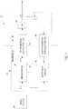
- Figure 2illustrates the main functional components of a digital predistorter 100 based on the modified V-DDR model given by Equation (0.3), which may be used as the predistorter 40 in Figure 1 .
- the predistorter 100comprises a first component modeling circuit 110, a second component modeling circuit 120, a conjugating circuit 130, a phase-shifting circuit 140, and a combining circuit 150.
- the first component modeling circuit 110applies a first non-linear function to a set of signal samples having different delays to produce a first component signal.
- the second component modeling circuit 120applies a second non-linear function to a set of second signal samples having different delays to produce a second component signal.
- the conjugating circuit 130computes conjugates of the first signal samples to produce the second signal samples.
- the phase-shifting circuit 140shifts the phase of one of the first and second component signals relative to the other. In the exemplary embodiment shown in Fig. 2 , the phase-shifting circuit 140 shifts the phase of the second component signal.
- the combining circuit 150combines the first component signal with the second component signal after the phase has been shifted to produce a predistorted input signal.
- the first component modeling circuit 110includes a tapped delay line 112 with Q+1 output taps 114, a series of multipliers 116, and a summation circuit 118.
- the input signal samplesare input to the tapped delay line.
- each delayrepresents a uniform one unit delay, i.e., one sample period.
- the computation of the weighting coefficientsmay use look-up tables.
- the summation circuit 118sums the outputs from the multipliers to produce the first component signal.
- the second component modeling circuit 120includes a tapped delay line 122 with Q output taps 124, a series of multipliers 126, and a summation circuit 128.
- the weighting coefficient for sample s 0is 0 so no output tap is needed.
- the conjugation circuit 130computes the conjugates of the first input signal samples, which are input to the tapped delay line 122. In the exemplary embodiment of Fig. 2 , each delay represents a uniform one unit delay, i.e., one sample period. Those skilled in the art will appreciate that more complex implementations may use non-unit and/or non-uniform delays.
- Multipliers 126multiply the samples on each output tap 124 by corresponding weighting coefficients.
- the computation of the weighting coefficientsmay use look-up tables.
- the summation circuit 128sums the outputs from the multipliers 126 to produce the second component signal.
- the phase shifting circuit 140shifts the phase of the second component signal by: x ⁇ n
- the summation circuit 150then adds the shifted second component signal and the first component signal sample-by-sample to produce the predistorted input signal ⁇ ( n ) .
- LUTslook-up tables
- LUT-based implementationsare cost effective, but to achieve good performance, a large number of entries to the LUT are needed. As a consequence, a large amount of data is required for training and coefficient configuration.
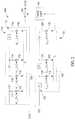
- the general predistorter structure 100 shown in Figure 2lends itself to implementation using look-up tables (LUTs) as shown in Figure 3 .
- the weighting coefficients w ⁇ i,j,p ( n ) computed in Equations (1.4) and (1.5)can be adapted by the adaptation circuit 60 to minimize the distortion.
- the adaptation circuit 60computes the weighting coefficients w ⁇ i,j,p ( n ) for the first and second modeling circuits 110, 120 jointly.
- Fig. 3illustrates a predistorter 200 that may be used as the predistorter 40 in Figure 1 .
- the predistorter 200comprises a first component modeling circuit 210, a second component modeling circuit 220, a conjugating circuit 230, a phase-shifting circuit 240, and a combining circuit 250.
- the first component modeling circuit 210applies a first non-linear function to a set of first signal samples having different delays to produce a first component signal.
- the second component modeling circuit 220applies a second non-linear function to a set of second signal samples having different delays to produce a second component signal.
- the conjugating circuit 230computes conjugates of the first signal samples to produce the second component signal.
- the phase-shifting circuit 240shifts the phase of one of the first and second component signals relative to the other. In the exemplary embodiment shown in Fig. 3 , the phase-shifting circuit 240 shifts the phase of the second component signal.
- the combining circuit 250combines the first component signal with the second component signal after the phase has been shifted to produce a predistorted input signal.
- the first component modeling circuit 210includes a tapped delay line 212 with Q+1 output taps 214, a series of multipliers 216, and a summation circuit 218.
- the input signal samplesare input to the tapped delay line 212.
- each delayrepresents a uniform one unit delay, i.e., one sample period.
- Multipliers 216multiply the samples on their respective output tap 214 by a corresponding weighting coefficient.
- a LUT unit 215is used to determine the weighting coefficient to be applied for each output tap 214 based on the current input sample.
- the summation circuit 218sums the outputs from the multipliers to produce the first component signal.
- the second component modeling circuit 220includes a tapped delay line 222 with Q output taps 224, a series of multipliers 226, and a summation circuit 228.
- the weighting coefficient for sample s 0is 0 so no output tap is needed.
- the conjugation circuit 230computes the conjugates of the first input signal samples, which are input to the tapped delay line 222.
- each delayrepresents a uniform one unit delay, i.e., one sample period.
- Multipliers 226multiply the samples on each output tap 224 by corresponding weighting coefficients.
- a LUT unit 225is used to determine the weighting coefficient to be applied for each output tap 214 based on the current input sample.
- the summation circuit 228sums the outputs from the multipliers 226 to produce the second component signal.
- the phase shifting circuit 240shifts the phase of the second component signal according to Equation (0.6).
- the summation circuit 250then adds the shifted second component signal and the first component signal sample-by-sample to produce the predistorted input signal ⁇ ( n ) .
- FIG 4illustrates an LUT unit 260 for the embodiment illustrated in Figure 3 .
- the LUT unit 260may be used to implement the LUT units 215, 225 shown in Figure 3 .
- the absolute value of the current input sample x ⁇ ( n )is input to the LUT unit 260.
- the LUT unit 260includes an address generator 262 and a LUT 264.
- the LUT 264stores pre-computed values of the weighting coefficients, which are calculated according to Equations (0.4) and (0.5).
- the address generator 262computes an address addr(n) based on the absolute value of the current input sample x ⁇ ( n ).
- the address addr(n)is then used as an index to retrieve one or more pre-computed coefficient values from the LUT 264.
- the LUT 264may be implemented as a single table for all weighting coefficients, or as individual tables for each weighting coefficient.
- FIG. 5illustrates an exemplary method 300 for predistorting an input signal according to one embodiment of the invention.
- a first non-linear component functionis applied input signal to generate a first component signal (block 310).
- the first non-linear functionoperates on a plurality of first signal samples with different delays.
- a second non-linear functionis applied to the conjugate of the input signal to generate a second component signal (block 320).
- the second non-linear functionoperates on a plurality of second signal samples with different delays.
- the second signal samplesare conjugates of the first signal samples.
- the phase of either the first component signal or the second component signalis shifted relative to the other (block 330).
- the first component signalis then combined with the second component signals to generate the predistorted output signal (block 340).
- the combiningis performed after the phase-shift operation.
- modified V-DDR approachcompared to a direct implementation based on power basis functions is that the dynamic order is consistent across all delayed terms, and the full degrees of freedom represented by the dynamic orders are provided.
- the modified V-DDR approachcan achieve better performance with lower complexity.
- the predistorter structure based on the modified V-DDR approachavoids square functions, which are required to implement first-order approximations in prior art designs. Instead of using square functions, the modified V-DDR approach can be implemented by a phase-shift, which can be effectively implemented by a CORDIC circuit.
Landscapes
- Engineering & Computer Science (AREA)
- Power Engineering (AREA)
- Physics & Mathematics (AREA)
- Nonlinear Science (AREA)
- Computer Networks & Wireless Communication (AREA)
- Signal Processing (AREA)
- Algebra (AREA)
- General Physics & Mathematics (AREA)
- Mathematical Analysis (AREA)
- Mathematical Optimization (AREA)
- Pure & Applied Mathematics (AREA)
- Amplifiers (AREA)
Description
- The present invention relates generally to digital predistortion for compensating an input signal for distortion introduced to the input signal by an electronic device and, more particularly, to a digital predistorter structure based on dynamic deviation reduction (DDR)-based Volterra series.
- The design of radio-frequency power amplifiers for communications applications often involves a trade-off between linearity and efficiency. Power amplifiers are typically most efficient when operated at or near their saturation point. However, the response of the amplifier at or near the point of saturation is non-linear. Generally speaking, when operating in the high-efficiency range, a power amplifier's response exhibits non-linearities and memory effects.
- One way to improve a power amplifier's efficiency and its overall linearity is to digitally predistort the input to the power amplifier to compensate for the distortion introduced by the power amplifier. In effect, the input signal is adjusted in anticipation of the distortion to be introduced by the power amplifier, so that the output signal is largely free of distortion products. Generally, the predistortion is applied to the signal digitally, at baseband frequencies, i.e., before the signal is upconverted to radio frequencies.
- These techniques can be quite beneficial in improving the overall performance of a transmitter system, in terms of both linearity and efficiency. Furthermore, these techniques can be relatively inexpensive, due to the digital implementation of the predistorter. In fact, with the availability of these techniques, power amplifiers may be designed in view of more relaxed linearity requirements than would otherwise be permissible, thus potentially reducing the costs of the overall system.
- Document
US 2004/239429 A1 may be construed to disclose a technique in which an input signal is modified to compensate for amplifier memory effects by combining at least two versions of the input signal, each version of the input signal being offset in time with respect to one another. More specifically, an RF input signal is split into at least two split signals, a different delay is applied to each split signal, and the delayed, split signals are combined to obtain a modified input signal. - Document "Behavioral Modeling of High Power RF Amplifiers Using Pruned Volterra Scheme with IIR Basis Functions", M. Masood et.al., may be construed to disclose a behavioral PA modeling scheme which combines existing pruned Volterra (PV) model with infinite impulse response (IIR) basis functions. These IIR basis functions are inherently composed of a parallel structure of single-pole IIR filters, summed at the output.
- The present invention provides a method and an apparatus according to the independent claims for predistorting an input signal to compensate for non-linearities in an electronic device that operates on the input signal. Developments are set forth in the dependent claims. The invention may be used, for example, to digitally predistort an input signal for a power amplifier in a wireless communication device. The predistorter uses a polynomial approach based on the well-known Volterra series to model the distortion function. A dynamic deviation reduction technique is used to reduce the number of terms in the distortion model and to facilitate implementation. The approach described herein eliminates square functions present in prior art designs and can be implemented using CORDIC circuits.
- Examples comprise methods of predistorting an input signal to an electronic device that operates on an input signal to generate an output signal. In one exemplary method, a first non-linear component function is applied to a set of first signal samples having different delays to generate a first component signal. A second non-linear component function is applied to a set of second signal samples having different delays to generate a second component signal. The second signal samples comprise conjugates of the first signal samples. The phase of one of the first and second component signals is shifted relative to the other. Following the relative phase shift of the first and second component signals, the first and second component signals are combined to generate a predistorted output signal.
- Other examples comprise a predistorter configured predistort an input signal to an electronic device, such as a power amplifier. The predistorter comprises a first component modeling circuit, a second component modeling circuit, a conjugating circuit, a phase-shifting circuit, and a combining circuit. The first component modeling circuit is configured to apply a first non-linear component function to a set of first signal samples having different delays to generate a first component signal. The second component modeling circuit is configured to apply a second non-linear component function to a set of second signal samples having different delays to generate a second component signal. The second signal samples are conjugates of the first signal samples. The phase adjustment circuit is configured to shift the phase of one of the first and second component signals relative to the other. The combining circuit is configured to combine the first and second component signals following the relative phase shift of the first and second component signals to generate a predistorted output signal.
- One advantage of the modified V-DDR approach described herein compared to a direct implementation based on the power basis functions is that the dynamic order is consistent across all delayed terms, and provides the full degrees of freedom represented by the dynamic orders. As a result, the modified V-DDR approach can achieve better performance with lower complexity. Also, the predistorter structure based on the modified V-DDR approach avoids square functions, which are required to implement first-order approximations in prior art designs. The modified V-DDR approach can be implemented by a phase-shift, which can be effectively implemented by a CORDIC circuit.
FIG. 1 illustrates an amplifier circuit including a digital predistorter according to embodiments of the present invention.FIG. 2 illustrates a digital predistorter according to one embodiment.Figure 3 illustrates a digital predistorter according to one embodiment using look-up tables.Figure 4 illustrates implementation of a look-up table for a digital predistorter.Figure 5 illustrates an exemplary method of digital predistortion.- Referring now to the drawings,
Figure 1 illustrates awireless terminal 10 for use in a mobile communication network. Thewireless terminal 10 includes asignal source 20 that generates a digital signal to be transmitted to a remote device (not shown), and anamplifier circuit 30. The digital signal is applied to the input of theamplifier circuit 30. Theamplifier circuit 30 includes adigital predistorter 40, transmitter front-end circuit 45,power amplifier 50,gain adjustment circuit 55, receiver front-end circuit 65, andadaptation circuit 60. The primary purpose of theamplifier circuit 30 is to amplify signals that are being transmitted. Thepower amplifier 50 is typically most efficient when it is operating in a non-linear range. However, the non-linear response of apower amplifier 50 causes out-of-band emissions and reduces spectral efficiency in a communication system. Therefore, adigital predistorter 40 may be used to improve power amplifier efficiency and linearity by predistorting the input signal to theamplifier circuit 30 to compensate for the non-linear distortion introduced by thepower amplifier 50. The cascading of apredistorter 40 andpower amplifier 50 improves the linearity of the output signal and thus allows thepower amplifier 50 to operate more efficiently. Theadaptation circuit 60 may be used to adapt thedigital predistorter 40. - Although predistortion is used in the circuits and systems described herein to linearize the output of a
power amplifier 50, those skilled in the art will appreciate that the techniques described are more generally applicable to linearize the output of any type of non-linear electronic device. - As seen in
Figure 1 , an input signalx̃(n) to theamplifier circuit 30 is input to thepredistorter 40. Thepredistorter 40 predistorts the input signalx̃(n) to compensate for the distortion introduced by thepower amplifier 50 when thepower amplifier 50 is operated in a non-linear range. The predistorted input signalũ(n) produced by thepredistorter 40 is upconverted, modulated and converted to analog form by the front-end circuit 45 and applied to the input of thepower amplifier 50. Thepower amplifier 50 amplifies the predistorted input signal to produce an output signaly(n). Ifpredistorter 40 is properly designed and configured, then the output signaly(n) contains fewer distortion products and out-of-band emissions than ifpower amplifier 50 were used alone. - A scaled version of the output signal, referred to as the feedback signal, is fed back to the
adaptation circuit 60 to adapt the coefficients of thepredistorter 40.Gain adjustment circuit 55 adjusts the gain of the feedback signal. The front-end circuit 65 downconverts, demodulates and converts the feedback signal to digital form for processing by theadaptation circuit 60. Theadaption circuit 60 compares the feedback signal with the original input signalx̃(n) and adjusts the coefficients of thepredistorter 40 to minimize the residual distortion products. - The distortion introduced by the
predistorter 40 orpower amplifier 50 can be represented by a complicated non-linear function, which will be referred to herein as the distortion function. One approach to modeling a distortion function, referred to herein as the polynomial approach, is to represent the distortion function as a set of less complicated basis functions and compute the output of the distortion function as the weighted sum of the basis functions. The set of basis functions used to model the distortion function is referred to herein as the basis function set. - Power amplifier models based on the Volterra series typically have high computational complexity. InZhu, Anding, et al, Dynamic Deviation Reduction-Based Volterra Behavioral Modeling of RF Power Amplifiers, IEEE Transactions on Microwave Theory and Techniques, Vol. 54, No. 12, Dec. 2006, a model order reduction method called dynamic deviation reduction (DDR) is used to significantly reduce the number of terms and thus the computational complexity of a power amplifier model. In this approach, the order of dynamics is explicitly distinguished from the order of non-linearity; the terms in the modified Volterra series are reorganized and the ones with high dynamic orders are removed. With this approach, the number of coefficients increases linearly with the order of non-linearly and memory length. Due to the reduction in complexity, this approach can be used to model a power amplifier.
- InZhu, Anding, Open-Loop Digital Predistorter for RF Power Amplifiers Using Dynamic Deviation Reduction-Based Volterra Series, IEEE Transactions on Microwave Theory and Techniques, Vol. 56, No. 7, July 2008, the V-DDR approach is applied to a digital predistorter. When the dynamic order is limited to the first order, the Volterra series model for a digital predistorter can be expressed as:

- The V-DDR approach represented by Equation (0.1) can be modified as follows:

- The modifications made to Equation (0.1) to arrive at Equation (0.2) include:
- 1. The order of summations is reversed
- 2. The coefficientg̃2k+1,2 = 0
- 3. Substitute

- In Equation (0.2), the terms


Figure 2 illustrates the main functional components of adigital predistorter 100 based on the modified V-DDR model given by Equation (0.3), which may be used as thepredistorter 40 inFigure 1 . (0.4). Thepredistorter 100 comprises a firstcomponent modeling circuit 110, a secondcomponent modeling circuit 120, a conjugatingcircuit 130, a phase-shiftingcircuit 140, and a combiningcircuit 150. The firstcomponent modeling circuit 110 applies a first non-linear function to a set of signal samples having different delays to produce a first component signal. The secondcomponent modeling circuit 120 applies a second non-linear function to a set of second signal samples having different delays to produce a second component signal. The conjugatingcircuit 130 computes conjugates of the first signal samples to produce the second signal samples. The phase-shiftingcircuit 140 shifts the phase of one of the first and second component signals relative to the other. In the exemplary embodiment shown inFig. 2 , the phase-shiftingcircuit 140 shifts the phase of the second component signal. The combiningcircuit 150 combines the first component signal with the second component signal after the phase has been shifted to produce a predistorted input signal.- The first
component modeling circuit 110 includes a tappeddelay line 112 with Q+1 output taps 114, a series ofmultipliers 116, and asummation circuit 118. The input signal samples are input to the tapped delay line. In the exemplary embodiment, each delay represents a uniform one unit delay, i.e., one sample period. Those skilled in the art will appreciate that more complex implementations may use non-unit and/or non-uniform delays.Multipliers 116 multiply the samples on eachoutput tap 114 by corresponding weighting coefficients. The weighting coefficients are computed for taps 0 through Q according to:
- As will be hereinafter described, the computation of the weighting coefficients may use look-up tables. The
summation circuit 118 sums the outputs from the multipliers to produce the first component signal. - The second
component modeling circuit 120 includes a tappeddelay line 122 with Q output taps 124, a series of multipliers 126, and asummation circuit 128. The weighting coefficient for samples0 is 0 so no output tap is needed. Theconjugation circuit 130 computes the conjugates of the first input signal samples, which are input to the tappeddelay line 122. In the exemplary embodiment ofFig. 2 , each delay represents a uniform one unit delay, i.e., one sample period. Those skilled in the art will appreciate that more complex implementations may use non-unit and/or non-uniform delays. Multipliers 126 multiply the samples on eachoutput tap 124 by corresponding weighting coefficients. The weighting coefficients are computed fortaps 1 through Q (there is no tap 0) according to:
- As will be hereinafter described, the computation of the weighting coefficients may use look-up tables. The
summation circuit 128 sums the outputs from the multipliers 126 to produce the second component signal. Thephase shifting circuit 140 shifts the phase of the second component signal by:
- The
summation circuit 150 then adds the shifted second component signal and the first component signal sample-by-sample to produce the predistorted input signalũ(n). - It is generally desirable to implement a digital predistorter using look-up tables (LUTs). LUT-based implementations are cost effective, but to achieve good performance, a large number of entries to the LUT are needed. As a consequence, a large amount of data is required for training and coefficient configuration. The
general predistorter structure 100 shown inFigure 2 lends itself to implementation using look-up tables (LUTs) as shown inFigure 3 . - The weighting coefficientsw̃i,j,p(n) computed in Equations (1.4) and (1.5) can be adapted by the
adaptation circuit 60 to minimize the distortion. When adapting thepredistorter 40, theadaptation circuit 60 computes the weighting coefficientsw̃i,j,p(n) for the first andsecond modeling circuits Fig. 3 illustrates apredistorter 200 that may be used as thepredistorter 40 inFigure 1 . Thepredistorter 200 comprises a firstcomponent modeling circuit 210, a secondcomponent modeling circuit 220, a conjugatingcircuit 230, a phase-shiftingcircuit 240, and a combiningcircuit 250. The firstcomponent modeling circuit 210 applies a first non-linear function to a set of first signal samples having different delays to produce a first component signal. The secondcomponent modeling circuit 220 applies a second non-linear function to a set of second signal samples having different delays to produce a second component signal. The conjugatingcircuit 230 computes conjugates of the first signal samples to produce the second component signal. The phase-shiftingcircuit 240 shifts the phase of one of the first and second component signals relative to the other. In the exemplary embodiment shown inFig. 3 , the phase-shiftingcircuit 240 shifts the phase of the second component signal. The combiningcircuit 250 combines the first component signal with the second component signal after the phase has been shifted to produce a predistorted input signal.- The first
component modeling circuit 210 includes a tapped delay line 212 with Q+1 output taps 214, a series ofmultipliers 216, and asummation circuit 218. The input signal samples are input to the tapped delay line 212. In the exemplary embodiment, each delay represents a uniform one unit delay, i.e., one sample period. Those skilled in the art will appreciate that more complex implementations may use non-unit and/or non-uniform delays.Multipliers 216 multiply the samples on theirrespective output tap 214 by a corresponding weighting coefficient. ALUT unit 215 is used to determine the weighting coefficient to be applied for eachoutput tap 214 based on the current input sample. Thesummation circuit 218 sums the outputs from the multipliers to produce the first component signal. - The second
component modeling circuit 220 includes a tappeddelay line 222 with Q output taps 224, a series ofmultipliers 226, and asummation circuit 228. As noted above, the weighting coefficient for samples0 is 0 so no output tap is needed. Theconjugation circuit 230 computes the conjugates of the first input signal samples, which are input to the tappeddelay line 222. In the exemplary embodiment, each delay represents a uniform one unit delay, i.e., one sample period. Those skilled in the art will appreciate that more complex implementations may use non-unit and/or non-uniform delays.Multipliers 226 multiply the samples on eachoutput tap 224 by corresponding weighting coefficients. ALUT unit 225 is used to determine the weighting coefficient to be applied for eachoutput tap 214 based on the current input sample. Thesummation circuit 228 sums the outputs from themultipliers 226 to produce the second component signal. - The
phase shifting circuit 240 shifts the phase of the second component signal according to Equation (0.6). Thesummation circuit 250 then adds the shifted second component signal and the first component signal sample-by-sample to produce the predistorted input signalũ(n). Figure 4 illustrates anLUT unit 260 for the embodiment illustrated inFigure 3 . TheLUT unit 260 may be used to implement theLUT units Figure 3 . The absolute value of the current input samplex̃(n) is input to theLUT unit 260. TheLUT unit 260 includes anaddress generator 262 and aLUT 264. TheLUT 264 stores pre-computed values of the weighting coefficients, which are calculated according to Equations (0.4) and (0.5). Theaddress generator 262 computes an addressaddr(n) based on the absolute value of the current input samplex̃(n). The addressaddr(n) is then used as an index to retrieve one or more pre-computed coefficient values from theLUT 264. TheLUT 264 may be implemented as a single table for all weighting coefficients, or as individual tables for each weighting coefficient.FIG. 5 illustrates anexemplary method 300 for predistorting an input signal according to one embodiment of the invention. A first non-linear component function is applied input signal to generate a first component signal (block 310). The first non-linear function operates on a plurality of first signal samples with different delays. A second non-linear function is applied to the conjugate of the input signal to generate a second component signal (block 320). The second non-linear function operates on a plurality of second signal samples with different delays. The second signal samples are conjugates of the first signal samples. The phase of either the first component signal or the second component signal is shifted relative to the other (block 330). The first component signal is then combined with the second component signals to generate the predistorted output signal (block 340). The combining is performed after the phase-shift operation.- One advantage of the modified V-DDR approach described herein compared to a direct implementation based on power basis functions is that the dynamic order is consistent across all delayed terms, and the full degrees of freedom represented by the dynamic orders are provided. As a result, the modified V-DDR approach can achieve better performance with lower complexity. Also, the predistorter structure based on the modified V-DDR approach avoids square functions, which are required to implement first-order approximations in prior art designs. Instead of using square functions, the modified V-DDR approach can be implemented by a phase-shift, which can be effectively implemented by a CORDIC circuit.
- The present invention may, of course, be carried out in other specific ways than those herein set forth without departing from the scope of the appended claims. The present embodiments are, therefore, to be considered in all respects as illustrative and not restrictive, and all changes coming within the scope of the appended claims are intended to be embraced therein.


Claims (15)
- A method (300) of predistorting an input signal based on a modified Volterra-Dynamic Deviation Reduction, V-DDR, model to compensate for non-linearities of an electronic device that operates on the input signal to produce a predistorted output signal, wherein the modified V-DDR model uses a polynomial approach to eliminate square functions in Volterra series according to the following equation:
 x̃(n) is the input signal;ũ(n) is the predistorted output signal;fi,1,p(|x̃(n)|) andfi,2,p(|x̃(n)|) are non-linear component functions expressed as even-order polynomials;the method comprising:applying (310) the first non-linear component function to a set of first signal samples having different delays to generate a first component signal;applying (320) the second non-linear component function to a set of second signal samples having different delays to generate a second component signal, wherein the second signal samples comprise conjugates of the first signal samples;shifting (330) the phase of one of the first and second component signals relative to the other, the shifted phase being dependent on a phase of the input signal; andcombining (340) the first and second component signals following the relative phase shift of the first and second component signals to generate the predistorted output signal.
 - The method (300) of claim 1 wherein applying a first non-linear component function to a set of first signal samples comprises:determining a weighting coefficient to be applied for each of the first signal samples; andmultiplying each of the first signal samples by its corresponding weighting coefficient and summing the products to produce the first component signal.
- The method (300) of claim 2 wherein:- determining a weighting coefficient to be applied for each of the first signal samples comprises determining the weighting coefficients from a lookup table; or- determining a weighting coefficient to be applied for each of the first signal samples comprises determining the weighting coefficient to be applied for each first signal sample based on a power basis function; or- determining a weighting coefficient to be applied for each of the first signal samples comprises determining the weighting coefficient to be applied for each first signal sample based on an orthogonal basis function.
- The method (300) of claim 1 wherein applying a second non-linear component function to a set of second signal samples comprises:determining a weighting coefficient to be applied for each of the second signal samples; andmultiplying each of the second signal samples by its corresponding weighting coefficient and summing the products to produce the second component signal.
- The method (300) of claim 4 wherein:- determining a weighting coefficient to be applied for each of the second signal samples comprises determining the weighting coefficients from a lookup table; or- determining a weighting coefficient to be applied for each of the second signal samples comprises determining the weighting coefficient to be applied for each second signal sample based on a power basis function; or- determining a weighting coefficient to be applied for each of the second signal samples comprises determining the weighting coefficient to be applied for each second signal sample based on an orthogonal basis function.
- The method (300) of claim 1 wherein:- the first and second non-linear component functions are applied to uniformly spaced signal samples with non-unit delays between adjacent samples; or- the first and second non-linear component functions are applied to non-uniformly spaced signal samples.
- A predistorter (100, 200) for predistorting an input signal to an electronic device based on a modified Volterra-Dynamic Deviation Reduction, V-DDR, model to compensate for non-linearities of the electronic device, wherein the modified V-DDR model uses a polynomial approach to eliminate square functions in Volterra series according to the following equation:
 x̃(n) is the input signal;ũ(n) is a predistorted output signal;fi,1,p(|x̃(n)|) andfi,2,p(|x̃(n)|) are non-linear component functions expressed as even-order polynomials;the predistorter (100, 200) comprising:a first component modeling circuit (110, 210) configured to apply the first non-linear component function to a set of first signal samples having different delays to generate a first component signal;a second component modeling circuit (120, 220) configured to apply the second non-linear component function to a set of second signal samples having different delays to generate a second component signal, wherein the second signal samples comprise conjugates of the first signal samples;a phase adjustment circuit (140, 240) configured to shift the phase of one of the first and second component signals relative to the other, the shifted phase being dependent on a phase of the input signal; anda combining circuit (150, 250) configured to combine the first and second component signals following the relative phase shift of the first and second component signals to generate the predistorted output signal.
 - The predistorter (100, 200) of claim 7 wherein the first component modeling circuit (110, 210) is configured to:determine a weighting coefficient to be applied for each of the first signal samples; andmultiply each of the first signal samples by its corresponding weighting coefficient and sum the products to produce the first component signal.
- The predistorter (100, 200) of claim 8 wherein the first component modeling circuit (110, 210) is configured to determine the weighting coefficients from a lookup table.
- The predistorter (100, 200) of claim 9 wherein:- the first component modeling circuit (110, 210) is configured to:
-- compute an address based on one or more of the first signal samples; and use the address as an index to one or more lookup tables to determine the weighting coefficients; or- the first component modeling circuit (110, 210) is configured to determine the weighting coefficients to be applied for each first signal sample based on a power basis function; or- the first component modeling circuit (110, 210) is configured to determine the weighting coefficients for each first signal sample based on an orthogonal basis function. - The predistorter (100, 200) of claim 7 wherein the second component modeling circuit (110, 210) is configured to:determine a weighting coefficient to be applied for each of the second signal samples; andmultiply each of the second signal samples by its corresponding weighting coefficient and sum the products to produce the second component signal.
- The predistorter (100, 200) of claim 11 wherein the second component modeling circuit (120, 220) is configured to determine the weighting coefficients from a lookup table.
- The predistorter (100, 200) of claim 12 wherein the second component modeling circuit is configured to:compute an address based on one or more of the second signal samples; anduse the address as an index to one or more lookup tables to determine the weighting coefficients.
- The predistorter (100, 200) of claim 11 wherein:- the second component modeling circuit (120, 220) is configured to determine the weighting coefficients to be applied for each second signal sample based on a power basis function; or- the second component modeling circuit (120, 220) is configured to determine the weighting coefficients to be applied for each second signal sample based on an orthogonal basis function.
- The predistorter (100, 200) of claim 7 wherein:- the first and second component modeling circuits (110, 210, 120, 220) are configured to apply the first and second non-linear component functions to uniformly spaced signal samples with non-unit delays between adjacent samples; or- wherein the first and second component modeling circuits (110, 210, 120, 220) are configured to apply the first and second non-linear component functions to non-uniformly spaced signal samples.


Applications Claiming Priority (2)
| Application Number | Priority Date | Filing Date | Title |
|---|---|---|---|
| US13/444,547US8564368B1 (en) | 2012-04-11 | 2012-04-11 | Digital Predistorter (DPD) structure based on dynamic deviation reduction (DDR)-based volterra series |
| PCT/IB2013/052640WO2013153485A1 (en) | 2012-04-11 | 2013-04-02 | Digital predistorter (dpd) structure based on dynamic deviation reduction (ddr)-based volterra series |
Publications (2)
| Publication Number | Publication Date |
|---|---|
| EP2837093A1 EP2837093A1 (en) | 2015-02-18 |
| EP2837093B1true EP2837093B1 (en) | 2018-06-06 |
Family
ID=48430887
Family Applications (1)
| Application Number | Title | Priority Date | Filing Date |
|---|---|---|---|
| EP13722568.6ANot-in-forceEP2837093B1 (en) | 2012-04-11 | 2013-04-02 | Digital predistorter (dpd) structure based on dynamic deviation reduction (ddr)-based volterra series |
Country Status (3)
| Country | Link |
|---|---|
| US (1) | US8564368B1 (en) |
| EP (1) | EP2837093B1 (en) |
| WO (1) | WO2013153485A1 (en) |
Families Citing this family (9)
| Publication number | Priority date | Publication date | Assignee | Title |
|---|---|---|---|---|
| US7796960B1 (en)* | 2006-04-04 | 2010-09-14 | Nortel Networks Limited | Signal transmitter linearization |
| KR20120070057A (en)* | 2010-12-21 | 2012-06-29 | 한국전자통신연구원 | Predistortion apparatus and method for the same |
| US8804872B1 (en)* | 2013-01-29 | 2014-08-12 | Texas Instruments Incorporated | Dynamic determination of volterra kernels for digital pre-distortion |
| US9184784B2 (en)* | 2014-03-10 | 2015-11-10 | Texas Instruments Incorporated | Method and apparatus for digital predistortion for a switched mode power amplifier |
| US9252821B2 (en) | 2014-06-27 | 2016-02-02 | Freescale Semiconductor, Inc. | Adaptive high-order nonlinear function approximation using time-domain volterra series to provide flexible high performance digital pre-distortion |
| US9628119B2 (en) | 2014-06-27 | 2017-04-18 | Nxp Usa, Inc. | Adaptive high-order nonlinear function approximation using time-domain volterra series to provide flexible high performance digital pre-distortion |
| US10153794B2 (en)* | 2016-12-02 | 2018-12-11 | Mediatek, Inc. | Transmitter, communication unit and method for limiting spectral re-growth |
| US10985951B2 (en) | 2019-03-15 | 2021-04-20 | The Research Foundation for the State University | Integrating Volterra series model and deep neural networks to equalize nonlinear power amplifiers |
| WO2021251852A1 (en)* | 2020-06-08 | 2021-12-16 | Telefonaktiebolaget Lm Ericsson (Publ) | Linearization of a non-linear electronic device |
Family Cites Families (10)
| Publication number | Priority date | Publication date | Assignee | Title |
|---|---|---|---|---|
| US6683495B2 (en)* | 2001-06-28 | 2004-01-27 | Simon Fraser University | Reduced architecture for multibranch feedforward power amplifier linearizers |
| SE520728C2 (en)* | 2001-11-12 | 2003-08-19 | Ericsson Telefon Ab L M | Non-linear modeling procedure |
| JP3872726B2 (en)* | 2002-06-12 | 2007-01-24 | 富士通株式会社 | Transmit amplifier |
| US7196578B2 (en) | 2003-05-30 | 2007-03-27 | Lucent Technologies Inc. | Amplifier memory effect compensator |
| WO2007046370A1 (en)* | 2005-10-17 | 2007-04-26 | Hitachi Kokusai Electric Inc. | Non-linear distortion detection method and distortion compensation amplification device |
| EP2005579A4 (en) | 2006-04-10 | 2017-02-22 | Telefonaktiebolaget LM Ericsson (publ) | A method and apparatus for reducing frequency memory effects in rf power amplifiers |
| US7724840B2 (en)* | 2006-12-19 | 2010-05-25 | Crestcom, Inc. | RF transmitter with predistortion and method therefor |
| US8005162B2 (en)* | 2007-04-20 | 2011-08-23 | Microelectronics Technology, Inc. | Dynamic digital pre-distortion system |
| US8369447B2 (en) | 2008-06-04 | 2013-02-05 | Apple Inc. | Predistortion with sectioned basis functions |
| US8351876B2 (en)* | 2010-08-03 | 2013-01-08 | Crestcom, Inc. | Transmitter linearized using cartesian-processed look-up table and method therefor |
- 2012
- 2012-04-11USUS13/444,547patent/US8564368B1/enactiveActive
- 2013
- 2013-04-02EPEP13722568.6Apatent/EP2837093B1/ennot_activeNot-in-force
- 2013-04-02WOPCT/IB2013/052640patent/WO2013153485A1/enactiveApplication Filing
Non-Patent Citations (1)
| Title |
|---|
| None* |
Also Published As
| Publication number | Publication date |
|---|---|
| US20130271212A1 (en) | 2013-10-17 |
| WO2013153485A1 (en) | 2013-10-17 |
| US8564368B1 (en) | 2013-10-22 |
| EP2837093A1 (en) | 2015-02-18 |
Similar Documents
| Publication | Publication Date | Title |
|---|---|---|
| US11129076B2 (en) | Method and system for baseband predistortion linearization in multi-channel wideband communication systems | |
| EP2837093B1 (en) | Digital predistorter (dpd) structure based on dynamic deviation reduction (ddr)-based volterra series | |
| US8787494B2 (en) | Modeling digital predistorter | |
| US8989307B2 (en) | Power amplifier system including a composite digital predistorter | |
| KR100789125B1 (en) | Wideband enhanced digital injection predistortion system and method | |
| EP2383886B1 (en) | Memory effect canceller, transmitter, and memory effect cancelling method | |
| US6956433B2 (en) | Polynomial predistorter using complex vector multiplication | |
| CN100477500C (en) | Power amplifier predistorter and base station comprising same | |
| US20040179629A1 (en) | Digital predistorter for a wideband power amplifier and adaptation method | |
| KR20040091706A (en) | Frequency-dependent magnitude pre-distortion for reducing spurious emissions in communication networks | |
| KR100487209B1 (en) | Predistortion apparatus and method for compensating non-linearility of the power amplifier using look-up table | |
| HK40047878A (en) | Method and system for baseband predistortion linearization in multi-channel wideband communication systems | |
| Ding et al. | Adaptive Linearization for Power Amplifier in OFDM Systems | |
| KR20020087503A (en) | Predistortion type digital linearizer and gain control method thereof |
Legal Events
| Date | Code | Title | Description |
|---|---|---|---|
| PUAI | Public reference made under article 153(3) epc to a published international application that has entered the european phase | Free format text:ORIGINAL CODE: 0009012 | |
| 17P | Request for examination filed | Effective date:20141007 | |
| AK | Designated contracting states | Kind code of ref document:A1 Designated state(s):AL AT BE BG CH CY CZ DE DK EE ES FI FR GB GR HR HU IE IS IT LI LT LU LV MC MK MT NL NO PL PT RO RS SE SI SK SM TR | |
| AX | Request for extension of the european patent | Extension state:BA ME | |
| DAX | Request for extension of the european patent (deleted) | ||
| GRAP | Despatch of communication of intention to grant a patent | Free format text:ORIGINAL CODE: EPIDOSNIGR1 | |
| STAA | Information on the status of an ep patent application or granted ep patent | Free format text:STATUS: GRANT OF PATENT IS INTENDED | |
| INTG | Intention to grant announced | Effective date:20180301 | |
| GRAS | Grant fee paid | Free format text:ORIGINAL CODE: EPIDOSNIGR3 | |
| GRAA | (expected) grant | Free format text:ORIGINAL CODE: 0009210 | |
| STAA | Information on the status of an ep patent application or granted ep patent | Free format text:STATUS: THE PATENT HAS BEEN GRANTED | |
| AK | Designated contracting states | Kind code of ref document:B1 Designated state(s):AL AT BE BG CH CY CZ DE DK EE ES FI FR GB GR HR HU IE IS IT LI LT LU LV MC MK MT NL NO PL PT RO RS SE SI SK SM TR | |
| REG | Reference to a national code | Ref country code:GB Ref legal event code:FG4D | |
| REG | Reference to a national code | Ref country code:CH Ref legal event code:EP Ref country code:AT Ref legal event code:REF Ref document number:1007151 Country of ref document:AT Kind code of ref document:T Effective date:20180615 | |
| REG | Reference to a national code | Ref country code:IE Ref legal event code:FG4D | |
| REG | Reference to a national code | Ref country code:DE Ref legal event code:R096 Ref document number:602013038551 Country of ref document:DE | |
| REG | Reference to a national code | Ref country code:NL Ref legal event code:MP Effective date:20180606 | |
| REG | Reference to a national code | Ref country code:LT Ref legal event code:MG4D | |
| PG25 | Lapsed in a contracting state [announced via postgrant information from national office to epo] | Ref country code:NO Free format text:LAPSE BECAUSE OF FAILURE TO SUBMIT A TRANSLATION OF THE DESCRIPTION OR TO PAY THE FEE WITHIN THE PRESCRIBED TIME-LIMIT Effective date:20180906 Ref country code:FI Free format text:LAPSE BECAUSE OF FAILURE TO SUBMIT A TRANSLATION OF THE DESCRIPTION OR TO PAY THE FEE WITHIN THE PRESCRIBED TIME-LIMIT Effective date:20180606 Ref country code:CY Free format text:LAPSE BECAUSE OF FAILURE TO SUBMIT A TRANSLATION OF THE DESCRIPTION OR TO PAY THE FEE WITHIN THE PRESCRIBED TIME-LIMIT Effective date:20180606 Ref country code:LT Free format text:LAPSE BECAUSE OF FAILURE TO SUBMIT A TRANSLATION OF THE DESCRIPTION OR TO PAY THE FEE WITHIN THE PRESCRIBED TIME-LIMIT Effective date:20180606 Ref country code:ES Free format text:LAPSE BECAUSE OF FAILURE TO SUBMIT A TRANSLATION OF THE DESCRIPTION OR TO PAY THE FEE WITHIN THE PRESCRIBED TIME-LIMIT Effective date:20180606 Ref country code:SE Free format text:LAPSE BECAUSE OF FAILURE TO SUBMIT A TRANSLATION OF THE DESCRIPTION OR TO PAY THE FEE WITHIN THE PRESCRIBED TIME-LIMIT Effective date:20180606 Ref country code:BG Free format text:LAPSE BECAUSE OF FAILURE TO SUBMIT A TRANSLATION OF THE DESCRIPTION OR TO PAY THE FEE WITHIN THE PRESCRIBED TIME-LIMIT Effective date:20180906 | |
| PG25 | Lapsed in a contracting state [announced via postgrant information from national office to epo] | Ref country code:LV Free format text:LAPSE BECAUSE OF FAILURE TO SUBMIT A TRANSLATION OF THE DESCRIPTION OR TO PAY THE FEE WITHIN THE PRESCRIBED TIME-LIMIT Effective date:20180606 Ref country code:RS Free format text:LAPSE BECAUSE OF FAILURE TO SUBMIT A TRANSLATION OF THE DESCRIPTION OR TO PAY THE FEE WITHIN THE PRESCRIBED TIME-LIMIT Effective date:20180606 Ref country code:GR Free format text:LAPSE BECAUSE OF FAILURE TO SUBMIT A TRANSLATION OF THE DESCRIPTION OR TO PAY THE FEE WITHIN THE PRESCRIBED TIME-LIMIT Effective date:20180907 Ref country code:HR Free format text:LAPSE BECAUSE OF FAILURE TO SUBMIT A TRANSLATION OF THE DESCRIPTION OR TO PAY THE FEE WITHIN THE PRESCRIBED TIME-LIMIT Effective date:20180606 | |
| REG | Reference to a national code | Ref country code:AT Ref legal event code:MK05 Ref document number:1007151 Country of ref document:AT Kind code of ref document:T Effective date:20180606 | |
| PG25 | Lapsed in a contracting state [announced via postgrant information from national office to epo] | Ref country code:NL Free format text:LAPSE BECAUSE OF FAILURE TO SUBMIT A TRANSLATION OF THE DESCRIPTION OR TO PAY THE FEE WITHIN THE PRESCRIBED TIME-LIMIT Effective date:20180606 | |
| PG25 | Lapsed in a contracting state [announced via postgrant information from national office to epo] | Ref country code:IS Free format text:LAPSE BECAUSE OF FAILURE TO SUBMIT A TRANSLATION OF THE DESCRIPTION OR TO PAY THE FEE WITHIN THE PRESCRIBED TIME-LIMIT Effective date:20181006 Ref country code:EE Free format text:LAPSE BECAUSE OF FAILURE TO SUBMIT A TRANSLATION OF THE DESCRIPTION OR TO PAY THE FEE WITHIN THE PRESCRIBED TIME-LIMIT Effective date:20180606 Ref country code:AT Free format text:LAPSE BECAUSE OF FAILURE TO SUBMIT A TRANSLATION OF THE DESCRIPTION OR TO PAY THE FEE WITHIN THE PRESCRIBED TIME-LIMIT Effective date:20180606 Ref country code:PL Free format text:LAPSE BECAUSE OF FAILURE TO SUBMIT A TRANSLATION OF THE DESCRIPTION OR TO PAY THE FEE WITHIN THE PRESCRIBED TIME-LIMIT Effective date:20180606 Ref country code:SK Free format text:LAPSE BECAUSE OF FAILURE TO SUBMIT A TRANSLATION OF THE DESCRIPTION OR TO PAY THE FEE WITHIN THE PRESCRIBED TIME-LIMIT Effective date:20180606 Ref country code:CZ Free format text:LAPSE BECAUSE OF FAILURE TO SUBMIT A TRANSLATION OF THE DESCRIPTION OR TO PAY THE FEE WITHIN THE PRESCRIBED TIME-LIMIT Effective date:20180606 Ref country code:RO Free format text:LAPSE BECAUSE OF FAILURE TO SUBMIT A TRANSLATION OF THE DESCRIPTION OR TO PAY THE FEE WITHIN THE PRESCRIBED TIME-LIMIT Effective date:20180606 | |
| PG25 | Lapsed in a contracting state [announced via postgrant information from national office to epo] | Ref country code:SM Free format text:LAPSE BECAUSE OF FAILURE TO SUBMIT A TRANSLATION OF THE DESCRIPTION OR TO PAY THE FEE WITHIN THE PRESCRIBED TIME-LIMIT Effective date:20180606 Ref country code:IT Free format text:LAPSE BECAUSE OF FAILURE TO SUBMIT A TRANSLATION OF THE DESCRIPTION OR TO PAY THE FEE WITHIN THE PRESCRIBED TIME-LIMIT Effective date:20180606 | |
| REG | Reference to a national code | Ref country code:DE Ref legal event code:R097 Ref document number:602013038551 Country of ref document:DE | |
| PLBE | No opposition filed within time limit | Free format text:ORIGINAL CODE: 0009261 | |
| STAA | Information on the status of an ep patent application or granted ep patent | Free format text:STATUS: NO OPPOSITION FILED WITHIN TIME LIMIT | |
| 26N | No opposition filed | Effective date:20190307 | |
| PG25 | Lapsed in a contracting state [announced via postgrant information from national office to epo] | Ref country code:DK Free format text:LAPSE BECAUSE OF FAILURE TO SUBMIT A TRANSLATION OF THE DESCRIPTION OR TO PAY THE FEE WITHIN THE PRESCRIBED TIME-LIMIT Effective date:20180606 Ref country code:SI Free format text:LAPSE BECAUSE OF FAILURE TO SUBMIT A TRANSLATION OF THE DESCRIPTION OR TO PAY THE FEE WITHIN THE PRESCRIBED TIME-LIMIT Effective date:20180606 | |
| PG25 | Lapsed in a contracting state [announced via postgrant information from national office to epo] | Ref country code:AL Free format text:LAPSE BECAUSE OF FAILURE TO SUBMIT A TRANSLATION OF THE DESCRIPTION OR TO PAY THE FEE WITHIN THE PRESCRIBED TIME-LIMIT Effective date:20180606 | |
| REG | Reference to a national code | Ref country code:CH Ref legal event code:PL | |
| REG | Reference to a national code | Ref country code:BE Ref legal event code:MM Effective date:20190430 | |
| PG25 | Lapsed in a contracting state [announced via postgrant information from national office to epo] | Ref country code:LU Free format text:LAPSE BECAUSE OF NON-PAYMENT OF DUE FEES Effective date:20190402 Ref country code:MC Free format text:LAPSE BECAUSE OF FAILURE TO SUBMIT A TRANSLATION OF THE DESCRIPTION OR TO PAY THE FEE WITHIN THE PRESCRIBED TIME-LIMIT Effective date:20180606 | |
| PG25 | Lapsed in a contracting state [announced via postgrant information from national office to epo] | Ref country code:LI Free format text:LAPSE BECAUSE OF NON-PAYMENT OF DUE FEES Effective date:20190430 Ref country code:CH Free format text:LAPSE BECAUSE OF NON-PAYMENT OF DUE FEES Effective date:20190430 | |
| PG25 | Lapsed in a contracting state [announced via postgrant information from national office to epo] | Ref country code:BE Free format text:LAPSE BECAUSE OF NON-PAYMENT OF DUE FEES Effective date:20190430 | |
| PG25 | Lapsed in a contracting state [announced via postgrant information from national office to epo] | Ref country code:TR Free format text:LAPSE BECAUSE OF FAILURE TO SUBMIT A TRANSLATION OF THE DESCRIPTION OR TO PAY THE FEE WITHIN THE PRESCRIBED TIME-LIMIT Effective date:20180606 | |
| PG25 | Lapsed in a contracting state [announced via postgrant information from national office to epo] | Ref country code:IE Free format text:LAPSE BECAUSE OF NON-PAYMENT OF DUE FEES Effective date:20190402 | |
| PG25 | Lapsed in a contracting state [announced via postgrant information from national office to epo] | Ref country code:PT Free format text:LAPSE BECAUSE OF FAILURE TO SUBMIT A TRANSLATION OF THE DESCRIPTION OR TO PAY THE FEE WITHIN THE PRESCRIBED TIME-LIMIT Effective date:20181008 | |
| PG25 | Lapsed in a contracting state [announced via postgrant information from national office to epo] | Ref country code:MT Free format text:LAPSE BECAUSE OF FAILURE TO SUBMIT A TRANSLATION OF THE DESCRIPTION OR TO PAY THE FEE WITHIN THE PRESCRIBED TIME-LIMIT Effective date:20180606 Ref country code:HU Free format text:LAPSE BECAUSE OF FAILURE TO SUBMIT A TRANSLATION OF THE DESCRIPTION OR TO PAY THE FEE WITHIN THE PRESCRIBED TIME-LIMIT; INVALID AB INITIO Effective date:20130402 | |
| PG25 | Lapsed in a contracting state [announced via postgrant information from national office to epo] | Ref country code:MK Free format text:LAPSE BECAUSE OF FAILURE TO SUBMIT A TRANSLATION OF THE DESCRIPTION OR TO PAY THE FEE WITHIN THE PRESCRIBED TIME-LIMIT Effective date:20180606 | |
| PGFP | Annual fee paid to national office [announced via postgrant information from national office to epo] | Ref country code:GB Payment date:20220427 Year of fee payment:10 Ref country code:FR Payment date:20220425 Year of fee payment:10 Ref country code:DE Payment date:20220427 Year of fee payment:10 | |
| REG | Reference to a national code | Ref country code:DE Ref legal event code:R119 Ref document number:602013038551 Country of ref document:DE | |
| GBPC | Gb: european patent ceased through non-payment of renewal fee | Effective date:20230402 | |
| PG25 | Lapsed in a contracting state [announced via postgrant information from national office to epo] | Ref country code:GB Free format text:LAPSE BECAUSE OF NON-PAYMENT OF DUE FEES Effective date:20230402 | |
| PG25 | Lapsed in a contracting state [announced via postgrant information from national office to epo] | Ref country code:GB Free format text:LAPSE BECAUSE OF NON-PAYMENT OF DUE FEES Effective date:20230402 Ref country code:FR Free format text:LAPSE BECAUSE OF NON-PAYMENT OF DUE FEES Effective date:20230430 Ref country code:DE Free format text:LAPSE BECAUSE OF NON-PAYMENT OF DUE FEES Effective date:20231103 |