EP2824484B1 - Metal detection method, metal detection device, metal detection method for wireless power supply device, and wireless power supply device - Google Patents
Metal detection method, metal detection device, metal detection method for wireless power supply device, and wireless power supply deviceDownload PDFInfo
- Publication number
- EP2824484B1 EP2824484B1EP13758119.5AEP13758119AEP2824484B1EP 2824484 B1EP2824484 B1EP 2824484B1EP 13758119 AEP13758119 AEP 13758119AEP 2824484 B1EP2824484 B1EP 2824484B1
- Authority
- EP
- European Patent Office
- Prior art keywords
- circuit
- power supplying
- metal
- arz
- metal detection
- Prior art date
- Legal status (The legal status is an assumption and is not a legal conclusion. Google has not performed a legal analysis and makes no representation as to the accuracy of the status listed.)
- Active
Links
- 239000002184metalSubstances0.000titleclaimsdescription229
- 238000001514detection methodMethods0.000titleclaimsdescription222
- 230000010355oscillationEffects0.000claimsdescription56
- 230000003321amplificationEffects0.000claimsdescription47
- 238000003199nucleic acid amplification methodMethods0.000claimsdescription47
- 230000005284excitationEffects0.000claimsdescription29
- 230000005674electromagnetic inductionEffects0.000claimsdescription9
- 230000008859changeEffects0.000claimsdescription6
- 239000000284extractSubstances0.000claimsdescription4
- 230000009466transformationEffects0.000claimsdescription4
- 238000012545processingMethods0.000description37
- 229910052755nonmetalInorganic materials0.000description21
- 239000003990capacitorSubstances0.000description15
- RKTYLMNFRDHKIL-UHFFFAOYSA-Ncopper;5,10,15,20-tetraphenylporphyrin-22,24-diideChemical compound[Cu+2].C1=CC(C(=C2C=CC([N-]2)=C(C=2C=CC=CC=2)C=2C=CC(N=2)=C(C=2C=CC=CC=2)C2=CC=C3[N-]2)C=2C=CC=CC=2)=NC1=C3C1=CC=CC=C1RKTYLMNFRDHKIL-UHFFFAOYSA-N0.000description10
- 238000000605extractionMethods0.000description10
- 230000004044responseEffects0.000description8
- 230000005540biological transmissionEffects0.000description7
- 238000004891communicationMethods0.000description7
- 238000010586diagramMethods0.000description7
- 230000004907fluxEffects0.000description6
- 230000000007visual effectEffects0.000description6
- 230000008901benefitEffects0.000description5
- 238000002474experimental methodMethods0.000description4
- 238000004364calculation methodMethods0.000description3
- 238000012360testing methodMethods0.000description3
- 230000000295complement effectEffects0.000description2
- 238000000034methodMethods0.000description2
- 230000000644propagated effectEffects0.000description2
- 239000000126substanceSubstances0.000description2
- 229920003002synthetic resinPolymers0.000description2
- 239000000057synthetic resinSubstances0.000description2
- 230000007423decreaseEffects0.000description1
- 238000007599dischargingMethods0.000description1
- 238000001914filtrationMethods0.000description1
- 230000006870functionEffects0.000description1
- 238000010438heat treatmentMethods0.000description1
- 238000005286illuminationMethods0.000description1
- 230000001939inductive effectEffects0.000description1
- 238000011112process operationMethods0.000description1
- 230000009467reductionEffects0.000description1
- 238000004088simulationMethods0.000description1
Images


Classifications
- G—PHYSICS
- G01—MEASURING; TESTING
- G01V—GEOPHYSICS; GRAVITATIONAL MEASUREMENTS; DETECTING MASSES OR OBJECTS; TAGS
- G01V3/00—Electric or magnetic prospecting or detecting; Measuring magnetic field characteristics of the earth, e.g. declination, deviation
- G01V3/08—Electric or magnetic prospecting or detecting; Measuring magnetic field characteristics of the earth, e.g. declination, deviation operating with magnetic or electric fields produced or modified by objects or geological structures or by detecting devices
- G01V3/10—Electric or magnetic prospecting or detecting; Measuring magnetic field characteristics of the earth, e.g. declination, deviation operating with magnetic or electric fields produced or modified by objects or geological structures or by detecting devices using induction coils
- H—ELECTRICITY
- H01—ELECTRIC ELEMENTS
- H01F—MAGNETS; INDUCTANCES; TRANSFORMERS; SELECTION OF MATERIALS FOR THEIR MAGNETIC PROPERTIES
- H01F38/00—Adaptations of transformers or inductances for specific applications or functions
- H01F38/14—Inductive couplings
- H—ELECTRICITY
- H02—GENERATION; CONVERSION OR DISTRIBUTION OF ELECTRIC POWER
- H02J—CIRCUIT ARRANGEMENTS OR SYSTEMS FOR SUPPLYING OR DISTRIBUTING ELECTRIC POWER; SYSTEMS FOR STORING ELECTRIC ENERGY
- H02J50/00—Circuit arrangements or systems for wireless supply or distribution of electric power
- H02J50/10—Circuit arrangements or systems for wireless supply or distribution of electric power using inductive coupling
- H02J50/12—Circuit arrangements or systems for wireless supply or distribution of electric power using inductive coupling of the resonant type
- H—ELECTRICITY
- H02—GENERATION; CONVERSION OR DISTRIBUTION OF ELECTRIC POWER
- H02J—CIRCUIT ARRANGEMENTS OR SYSTEMS FOR SUPPLYING OR DISTRIBUTING ELECTRIC POWER; SYSTEMS FOR STORING ELECTRIC ENERGY
- H02J50/00—Circuit arrangements or systems for wireless supply or distribution of electric power
- H02J50/40—Circuit arrangements or systems for wireless supply or distribution of electric power using two or more transmitting or receiving devices
- H02J50/402—Circuit arrangements or systems for wireless supply or distribution of electric power using two or more transmitting or receiving devices the two or more transmitting or the two or more receiving devices being integrated in the same unit, e.g. power mats with several coils or antennas with several sub-antennas
- H—ELECTRICITY
- H02—GENERATION; CONVERSION OR DISTRIBUTION OF ELECTRIC POWER
- H02J—CIRCUIT ARRANGEMENTS OR SYSTEMS FOR SUPPLYING OR DISTRIBUTING ELECTRIC POWER; SYSTEMS FOR STORING ELECTRIC ENERGY
- H02J50/00—Circuit arrangements or systems for wireless supply or distribution of electric power
- H02J50/60—Circuit arrangements or systems for wireless supply or distribution of electric power responsive to the presence of foreign objects, e.g. detection of living beings
- H—ELECTRICITY
- H04—ELECTRIC COMMUNICATION TECHNIQUE
- H04B—TRANSMISSION
- H04B5/00—Near-field transmission systems, e.g. inductive or capacitive transmission systems
- H04B5/70—Near-field transmission systems, e.g. inductive or capacitive transmission systems specially adapted for specific purposes
- H04B5/79—Near-field transmission systems, e.g. inductive or capacitive transmission systems specially adapted for specific purposes for data transfer in combination with power transfer
- H—ELECTRICITY
- H02—GENERATION; CONVERSION OR DISTRIBUTION OF ELECTRIC POWER
- H02J—CIRCUIT ARRANGEMENTS OR SYSTEMS FOR SUPPLYING OR DISTRIBUTING ELECTRIC POWER; SYSTEMS FOR STORING ELECTRIC ENERGY
- H02J7/00—Circuit arrangements for charging or depolarising batteries or for supplying loads from batteries
- H02J7/0068—Battery or charger load switching, e.g. concurrent charging and load supply
Definitions
- the present inventionrelates to a metal detection method for a contactless power supplying device, and a contactless power supplying device.
- an electromagnetic induction type contactless power transmission deviceincludes a metal detection device.
- the metal detection deviceprevents the metal from being inductively heated when supplying power to an electric instrument.
- a metal detection deviceis a frequency following circuit that searches for a resonance frequency to determine whether (1) nothing is placed on the setting surface, (2) a power receiving circuit is correctly placed on the setting surface, and (3) a foreign object of metal or the like is placed on the setting surface.
- a metal detection devicemonitors changes in the amplitude of a coil voltage caused by load modulation to detect a foreign object of metal or the like.
- a metal detection devicechanges a signal applied to a primary coil between two intensities and monitors the power consumed at the primary side to check whether a foreign object exists on the setting surface.
- JP 2000/295796if metal is sandwiched between the power supplying circuit and the correct power receiving circuit, a strong influence resulting from the arrangement of the correct power receiving circuit makes it difficult to determination whether or not metal exists. That is, since the difference between the frequency of when a metal is placed and the frequency of when a correct power receiving circuit is placed is small, it is difficult to detect the metal sandwiched between the power supplying circuit and the correct power receiving circuit.
- JP 2011/507481changes in the intensity of a fundamental wave are monitored.
- the amount of change in the fundamental waveis very small with respect to a metal. This makes the determination difficult.
- the signal intensityis changed between two levels, two power supplies are required. This is disadvantageous in terms of cost and size.
- US 2012/0001493 A1discloses a power transmission system and a power transmission apparatus as well as a foreign-substance detecting unit, which detects the presence of a foreign substance by shift of a first peaking frequency.
- WO 2013/012088 A1shows a detection device that includes a coil configured to be electromagnetically coupled with an outside, and a detection section connected to a circuit including the coil.
- the detection sectionis configured to measure a Q value of the circuit using an alternating-current signal at a frequency different from a frequency of an alternating-current signal of contactless power feed.
- contactless power supplying devicehave become popular, and the range of the field and usage environment of the subject supplied with power by the contactless power supplying device has become wide.
- a new metal detection methodother than the methods described above, having high accuracy and unaffected by the usage environment.
- a new type of metal detection method and a detection device thereofare desired for a metal detection device that detects in a contactless manner whether an object is a metal or a non-metal such as a synthetic resin.
- a metal detection method of a contactless power supplying deviceuses a contactless power supplying device including a primary coil arranged in a power supplying area.
- the contactless power supplying deviceexcites the primary coil arranged in the power supplying area to cause electromagnetic induction at a secondary coil of a power receiving device arranged in the electric instrument and supply power to the electric instrument.
- the contactless power supplying deviceincludes a metal detection coil arranged in the power supplying area.
- the metal detection methodincludes exciting the metal detection coil with a sinusoidal oscillating current having a single fundamental frequency to radiate an electromagnetic wave from the metal detection coil, and detecting whether or not metal exists in the power supplying area from a change in a fundamental frequency of the oscillating current flowing to the metal detection coil.
- the detecting whether or not metal exists in the power supplying areaincludes detecting that metal exists in the power supplying area when a harmonic of the fundamental frequency is generated in the oscillating current.
- a contactless power supplying devicearranges a primary coil in a power supplying area.
- the primary coil arranged in the power supplying areais excited to cause electromagnetic induction at a secondary coil of a power receiving device arranged in the electric instrument to supply power to the electric instrument.
- a metal detection coilis arranged in the power supplying area.
- An oscillation circuitgenerates a sinusoidal oscillating current having a single fundamental frequency and supplies the oscillating current to the metal detection coil to excite the metal detection coil.
- a harmonic level detection circuitdetects a harmonic component of the fundamental frequency component of the oscillating current and generates a detection signal.
- a comparison circuitcompares a signal level of the detection signal and a reference value, which is set in advance.
- a control circuitdetermines whether or not metal exists in the power supplying area based on a comparison result. When determining that metal exists in the power supplying area, the control circuit causes the oscillation circuit to stop the excitation of the metal detection coil.
- the harmonic level detection circuitincludes a filter circuit that filters a frequency component higher than the fundamental frequency from the oscillating current to generate a filtered signal, and an amplification circuit that amplifies the filtered signal from the filter circuit and generates the detection signal.
- the harmonic level detection circuitincludes a high speed Fourier transformation circuit that extracts a frequency component higher than the fundamental frequency from the oscillating current and generates the detection signal.
- the power supplying areais one of a plurality of separate power supplying areas.
- the primary coilis one of a plurality of primary coils respectively arranged in the plurality of power supplying areas.
- the metal detection coilis one of a plurality of metal detection coils respectively arranged in the plurality of power supplying areas.
- the oscillation circuitis one of a plurality of oscillation circuits respectively arranged in the plurality of power supplying areas.
- the harmonic level detection circuitis one of a plurality of harmonic level detection circuits respectively arranged in the plurality of power supplying areas.
- the comparison circuitis one of a plurality of comparison circuits respectively arranged in the plurality of power supplying areas.
- the contactless power supplying deviceincludes a plurality of metal detection circuits respectively arranged in the plurality of power supplying areas.
- Each of the plurality of metal detection circuitsincludes the oscillation circuit, the harmonic level detection circuit, and the comparison circuit, and is controlled by the control circuit.
- the above configurationincludes a notification unit that indicates whether or not metal exists in the power supplying area.
- the control circuitdrives the notification unit based on a comparison result of the comparison circuit.
- the notification unitincludes an indication lamp.
- the metal detection device of this first examplecan be used with the contactless power supplying device of the invention.
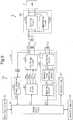
- a metal detection device 1includes a tetragonal plate-shaped housing 2, and a planar setting surface 3, which is formed on an upper surface of the housing 2 and on which an object OB is placed.
- a single tetragonal detection area ARis defined in the setting surface 3.
- the metal detection device 1detects, in a contactless manner, whether the object OB placed on the setting surface 3 is a metal or a non-metal such as a synthetic resin or the like.
- a metal detection coil Lswhich is wound to have a tetragonal shape in conformance with the outer shape of the detection area AR, is arranged in the housing 2 at a position corresponding to the detection area AR.
- the metal detection coil Ls of the detection area ARis connected to an oscillation circuit 10 (see Fig. 3 ) arranged in the housing 2.
- the metal detection coil Ls of the detection area ARis excited by the oscillation circuit 10.
- the metal detection coil Lsis excited to detect whether the object OB placed in the detection area AR is a metal or a non-metal.
- a power switch 6is arranged on the setting surface 3.
- the metal detection device 1performs detections when the power switch 6 is operated.
- a indication lamp 7is also arranged on the setting surface 3. The indication lamp 7 indicates the detection result.
- the metal detection device 1includes an oscillation circuit 10, a harmonic level detection circuit 11, a comparison circuit 12, and a processing circuit 13.
- the oscillation circuit 10is configured by a Colpitts oscillation circuit, and the metal detection coil Ls also functions as one of the components configuring the oscillation circuit 10.
- the oscillation circuit 10includes a bipolar transistor Q1, the metal detection coil Ls, first to third capacitors C1 to C3, and a resistor R.
- a collector terminalis connected to one end of the metal detection coil Ls, and a base terminal is connected to a positive terminal of a DC voltage Vdd via a parallel circuit including the third capacitor C3 and the resistor R. Further, in the bipolar transistor Q1, an emitter terminal is grounded and also connected to the other end of the metal detection coil Ls via the first capacitor C1.
- the second capacitor C2is connected between the collector and emitter terminals of the bipolar transistor Q1.
- the other end of the metal detection coil Lsis connected to the positive terminal of the DC voltage Vdd.
- the oscillation circuit 10When the DC voltage Vdd is applied to the oscillation circuit 10, the oscillation circuit 10 is oscillated.
- a sinusoidal oscillating current It having a single fundamental frequencyflows from the collector terminal of the bipolar transistor Q1 to the metal detection coil Ls and excites the metal detection coil Ls.
- the metal detection coil Lsthus radiates a sinusoidal electromagnetic wave having the single fundamental frequency.
- the single fundamental frequency oscillated by the oscillation circuit 10is set in advance by the components configuring the oscillation circuit 10.
- the fundamental frequencyis set in advance by a circuit constant of the bipolar transistor Q1, the metal detection coil Ls, the first to third capacitors C1 to C3, and the resistor R of the oscillation circuit 10.
- the fundamental frequencyis set so that when a non-metal object OB is placed on the setting surface 3, the metal detection coil Ls and the non-metal object OB oscillate, or match.
- the metal detection coil Ls and the object OBare matched.
- a reflected wave from the non-metal object OB to the metal detection coil Lsdoes not exist.
- the sinusoidal oscillating current It having the fundamental frequency flowing to the metal detection coil Lsis not distorted. That is, the sinusoidal oscillating current It having the fundamental frequency does not contain harmonic components (second harmonic, third harmonic, etc.) of the fundamental frequency that would result from distortion of the oscillating current It when the fundamental frequency is disturbed.
- the metal detection coil LsWhen nothing is placed in the detection area AR (when a non-metal object OB is not placed in the detection area AR), the metal detection coil Ls is not spatially coupled with the object OB, and a reflecting wave to the metal detection coil Ls does not exist. As a result, the oscillating current It flowing to the metal detection coil Ls is not distorted, and the oscillating current It does not contain harmonic components (second harmonic, third harmonic, etc.) of the fundamental frequency.
- metalWhen a metal object OB is placed on the setting surface 3, metal receives the magnetic energy of the electromagnetic wave having the fundamental frequency from the metal detection coil Ls, and an eddy current is generated in the metal.
- the influence of magnetic flux accompanying the eddy current generated in the metalproduces noise that disturbs the fundamental frequency.
- the existence of a metalresults in a mismatching, and some of the energy of the electromagnetic wave radiated from the metal detection coil Ls is reflected from the metal toward the metal detection coil Ls.
- the fundamental frequency of the oscillating current Itis disturbed, and the oscillating current It is distorted and contains the harmonic components (second harmonic, third harmonic, etc.) of the fundamental frequency.
- the harmonic componentsare high-order frequency components (second harmonic, third harmonic, etc.) of integral multiples of the fundamental frequency.
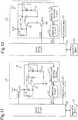
- the harmonic level detection circuit 11is connected to the collector terminal of the bipolar transistor Q1.
- the oscillating current Itis supplied to the harmonic level detection circuit 11 from the collector terminal of the bipolar transistor Q1.
- the harmonic level detection circuit 11includes a high pass filter circuit 11a and an amplification circuit 11b.
- the oscillating current Itis supplied from the collector terminal of the bipolar transistor Q1 to the high pass filter circuit 11a.
- the high pass filter circuit 11aremoves the current component of the fundamental frequency contained in the oscillating current It, and filters the current component of the harmonic (second harmonic, third harmonic, etc.) of the fundamental frequency contained in the oscillating current It to generate a filtered signal SHF, and provides the filtered signal SHF to the amplification circuit 11b.
- the high pass filter circuit 11aprovides the filtered signal SHF including the harmonic components (second harmonic, third harmonic, etc.) other than the fundamental frequency components to the amplification circuit 11b.
- the fundamental frequency of the oscillating current Itis not be distorted.
- the oscillating current Itdoes not contain harmonic components other than the fundamental frequency components, and the filtered signal SHF is not provided to the amplification circuit 11b.
- the fundamental frequency of the oscillating current Itis not distorted.
- the oscillating current Itdoes not contain harmonic components other than the fundamental frequency components, and the filtered signal SHF is not provided to the amplification circuit 11b.
- the high pass filter circuit 11aprovides the filtered signal SHF including the harmonic components (second harmonic, third harmonic, etc.) of the oscillating current It to the amplification circuit 11b.
- the amplification circuit 11bis, for example, an inverted amplification circuit, a noninverted amplification circuit, and the like.
- the amplification circuit 11bamplifies the filtered signal SHF including the harmonic components (second harmonic, third harmonic, etc.) at a gain set in advance, and provides the filtered signal SHF to the comparison circuit 12 as a detection voltage Vs.
- the comparison circuit 12includes a comparator circuit 12a, which is formed by an operational amplifier, and a reference voltage generation circuit 12b.
- the detection voltage Vsis supplied to one input terminal from the amplification circuit 11b, and a reference voltage Vk is supplied to the other input terminal from the reference voltage generation circuit 12b.
- the reference voltage Vkis a voltage at which the detection voltage Vs can be detected in the comparator circuit 12a when a metal object OB is placed on the setting surface 3.
- the reference voltage Vkis set in advance based on experiments, tests, calculations, and the like.
- the comparator circuit 12acompares the detection voltage Vs and the reference voltage Vk. When the detection voltage Vs is greater than or equal to the reference voltage Vk, the comparator circuit 12a provides a determination signal SGJ having high level, which indicates that a metal object OB is placed in the detection area AR, to the processing circuit 13. In contrast, when the detection voltage Vs is lower than the reference voltage Vk, the comparator circuit 12a provides the determination signal SGJ having a low level, which indicates that a metal object OB is not placed in the detection area AR, to the processing circuit 13.
- the processing circuit 13is configured by a micro-computer.
- the determination signal SGJis provided from the comparator circuit 12a to the processing circuit 13.
- the processing circuit 13continuously illuminates the indication lamp 7 arranged on the setting surface 3 in red. This allows for visual recognition of a metal object OB placed on the setting surface 3.
- the processing circuit 13continuously illuminates the indication lamp 7 in blue. This allows for visual recognition of a non-metal object OB placed on the setting surface 3 or nothing placed on the setting surface 3.
- the DC voltage Vddis applied to the oscillation circuit 10. This oscillates the oscillation circuit 10.
- the oscillating current It having the fundamental frequencythen flows from the collector terminal of the bipolar transistor Q1 to the metal detection coil Ls, thus exciting the metal detection coil Ls.
- the fundamental frequency of the oscillating current Itis not disturbed, and the oscillating current It does not contain harmonic components other than the fundamental frequency components.
- the oscillating current It of the fundamental frequency componentis removed by the high pass filter circuit 11a, and the filtered signal SHF is not provided to the amplification circuit 11b.
- the amplification circuit 11bsupplies the comparator circuit 12a with the detection voltage Vs that is lower than the reference voltage Vk.
- the comparator circuit 12aprovides the determination signal SGJ having a low level, which indicates that the metal object OB is not placed in the detection area AR, to the processing circuit 13.
- the processing circuit 13then continuously illuminates the indication lamp 7 in blue in response to the determination signal SGJ having a low level, so that it can be visually recognized that nothing exists on the setting surface 3.
- the fundamental frequency of the oscillating current Itis not disturbed, and hence the oscillating current It does not contain harmonic components other than the fundamental frequency components like when nothing exists on the setting surface 3.
- the oscillating current It of the fundamental frequency componentis removed by the high pass filter circuit 11a, and the filtered signal SHF is not provided to the amplification circuit 11b.
- the processing circuit 13continuously illuminates the indication lamp 7 in blue so that the non-metal object OB placed on the setting surface 3 can be visually recognized.
- the high pass filter circuit 11aprovides the filtered signal SHF including the harmonic components (second harmonic, third harmonic, etc.) other than the fundamental frequency components to the amplification circuit 11b.
- the detection voltage Vs having a voltage value greater than the reference voltage Vkis supplied from the amplification circuit 11b to the comparator circuit 12a.
- the comparator circuit 12aprovides the determination signal SGJ having a high level, which indicates that a metal object OB exists in the detection area AR, to the processing circuit 13.
- the processing circuit 13continuously illuminates the indication lamp 7 in red in response to the determination signal SGJ having a high level so that the metal object OB placed on the setting surface 3 can be visually recognized.
- the first examplehas the following advantages.
- a contactless power supplying devicewill now be described with reference to the drawings.
- the feature of the embodimentis in that the metal detection device of the first example is applied to a contactless power supplying device.
- the featurewill be described in detail, and portions that are the same as the first example will be illustrated with the same reference numerals for the sake of convenience.
- Fig. 4is a perspective view entirely showing a contactless power supplying device (hereinafter referred to as the power supplying device) 21 and an electric instrument (hereinafter referred to as the instrument) E that is supplied with power in a contactless manner from the power supplying device 21.
- the power supplying device 21a contactless power supplying device
- the instrumentan electric instrument
- the power supplying device 21includes a tetragonal plate-shaped housing 22 and a planar setting surface 23, which is formed on an upper surface of the housing 22.
- the instrument Eis placed on the setting surface 23.
- a single tetragonal power supplying area ARzis defined in the setting surface 23.
- a primary coil L1which is wound to have a tetragonal shape in conformance with the outer shape of the detection area ARz, is arranged in the housing 22 at a position corresponding to the detection area ARz.
- the primary coil L1is connected to a power supplying unit circuit 34 (see Fig. 6 ) arranged in the housing 22.
- the primary coil L1is excited by the power supplying unit circuit 34.
- the primary coil L1is excited to detect whether or not the instrument E is placed in the power supplying area ARz and to cause electromagnetic induction at a secondary coil L2 in the instrument E to supply the instrument E with power in a contactless manner.
- a metal detection coil Lswhich is wound to have a tetragonal shape in conformance with the outer shape of the primary coil L1, is arranged at the inner side of the primary coil L1 at a position corresponding to the power supplying area ARz.
- the metal detection coil Lsis connected to the oscillation circuit 10 (see Fig. 6 ), which is arranged in the housing 22.
- the metal detection coil Ls of the power supplying area ARzis excited by the oscillation circuit 10.
- the metal detection coil Lsis excited to detect whether or not a metal object OB has been placed in the power supplying area ARz.
- a power switch 26is also arranged on the setting surface 23.
- the contactless power supplying device 21can supply power in a contactless manner when the power switch 26 is operated.
- a indication lamp 27is also arranged on the setting surface 23. The indication lamp 27 indicates the operation state of the contactless power supplying device 21.
- the instrument Eincludes a power receiving circuit 28, which serves as a power receiving device that receives secondary power from the power supplying device 21, and a load Z.
- the power receiving circuit 28includes a rectifying circuit 28a and a communication circuit 28b.
- the rectifying circuit 28ais connected to the secondary coil L2 via a resonance capacitor Cx.
- electromagnetic inductionwhich results from the excitation of the primary coil L1 of the power supplying device 21, generates secondary power.
- the rectifying circuit 28aconverts the secondary power, which is generated in the secondary coil L2, to a ripple-free DC voltage.
- the rectifying circuit 28asupplies the DC voltage to the load Z of the instrument E.
- the load Zis driven using the secondary power generated be the secondary coil L2.
- the instrument Emay use the DC power converted by the rectifying circuit 28a to drive the load Z on the setting surface 23.
- the instrument Emay use AC power as the secondary power to drive the load Z on the setting surface 23.
- the instrument Emay also charge a built-in rechargeable battery (secondary battery) using the DC power supply converted by the rectifying circuit 28a.
- the communication circuit 28buses the DC voltage from the rectifying circuit 28a as a drive source.
- the communication circuit 28bgenerates an instrument authentication signal ID and an excitation request signal RQ, and transmits the signals to the power supplying device 21 via the secondary coil L2.
- the instrument authentication signal IDis an authentication signal that indicates that the instrument E is allowed to be supplied with power from the power supplying device 21.
- the excitation request signal RQis a request signal that requests the power supplying device 21 to be supplied with power.
- the communication circuit 28bwhen the power switch for driving the load Z arranged in the instrument E is switched OFF, the communication circuit 28b does not generate the instrument authentication signal ID and the excitation request signal RQ. Furthermore, if a microcomputer is arranged in the instrument E, the communication circuit 28b does not generate the instrument authentication signal ID and the excitation request signal RQ when the microcomputer determines to suspend the power supply.
- the instrument authentication signal ID and the excitation request signal RQinclude bits and are binarized (high level/low level).
- the instrument authentication signal ID and the excitation request signal RQare provided to a power receiving line that connects the resonance capacitor Cx and the rectifying circuit 28a.
- the amplitude of the secondary current flowing to the secondary coil L2is changed based on the instrument authentication signal ID and the excitation request signal RQ provided to the power supplying line.
- the amplitude of the magnetic flux radiated from the secondary coil L2changes in accordance with the change in amplitude of the secondary current.
- the changed magnetic fluxis propagated to the primary coil L1 as electromagnetic induction thus changing the amplitude of the primary current flowing to the primary coil L1.
- the secondary current flowing between the terminals of the secondary coil L2is amplitude-modulated by the binary signals (instrument authentication signal ID and excitation request signal RQ).
- the magnetic flux of the amplitude modulated secondary currentis propagated to the primary coil L1 as a transmission signal.
- the power supplying device 21includes a power supply circuit 31, a system control circuit 32, a nonvolatile memory 33 that stores various types of data, and a power supplying unit circuit 34.
- the power supply circuit 31includes a rectifying circuit and a DC/DC converter.
- a commercial power supplyis externally supplied to the power supply circuit 31.
- the power supply circuit 31rectifies the supplied commercial power supply in the rectifying circuit.
- the power supply circuit 31converts the rectified DC voltage to the desired DC voltage Vdd in the DC/DC converter, and then supplies the DC voltage Vdd to the system control circuit 32 and the nonvolatile memory 33 as the drive power supply.
- the power supply circuit 31also supplies the DC voltage Vdd to the power supplying unit circuit 34 as the drive power supply.
- the system control circuit 32includes a microcomputer, and controls the power supplying unit circuit 34.
- the nonvolatile memory 33stores various types of data used when the system control circuit 32 performs various determination process operations.
- the power supplying unit circuit 34exchanges data with the system control circuit 32, and is controlled by the system control circuit 32.
- the power supplying unit circuit 34includes a full-bridge circuit 41, a drive circuit 42, a primary current detection circuit 43, a signal extraction circuit 44, and a metal detection circuit 45.
- the full-bridge circuit 41is a known full-bridge circuit. As shown in Fig. 7 , the full-bridge circuit 41 includes four N-channel MOS transistors Qa, Qb, Qc, and Qd. The four MOS transistors Qa, Qb, Qc, and Qd are divided into the pair of the MOS transistors Qa and Qd and the pair of the MOS transistors Qb and Qc are bridged by a series circuit including the primary coil L1 and the resonance capacitor C in between. The primary coil L1 is excited by alternately switching ON and OFF the two pairs.
- An excitation control signal CTis provided from the system control circuit 32 to the drive circuit 42.
- the drive circuit 42generates four drive signals PSa, PSb, PSc, and PSd provided to the gate terminals of the four MOS transistors Qa, Qb, Qc, and Qd, respectively.
- the drive circuit 42When supplying power to the instrument E, the drive circuit 42 alternately switches ON and OFF (full-bridge operation) the two pairs based on the excitation control signal CT from the system control circuit 32 to generate the four drive signals PSa, PSb, PSc, and PSd for exciting the primary coil L1.
- the drive circuit 42provides the two drive signals PSa and PSd, which having the same pulse waveform, respectively to the two gate terminals of the MOS transistors Qa and Qd in the first pair.
- the drive circuit 42also provides the two drive signals PSb and PSc, which are complementary signals of the two drive signals PSa and PSd and have the same pulse waveform, respectively to the two gate terminals of the MOS transistors Qb and Qc in the second pair.
- the primary coil L1is excited by alternately turning ON and OFF (full-bridge operation) the first pair of the MOS transistors Qa and Qd and the second pair of the MOS transistors Qb and Qc.
- the drive circuit 42When supplying power to the instrument E, the drive circuit 42 alternately switches ON and OFF (full-bridge operation) the two pairs based on the excitation control signal CT from the system control circuit 32 to generate the four drive signals PSa, PSb, PSc, and PSd for exciting the primary coil L1.
- the drive circuit 42Under a standby condition, the drive circuit 42 generates the four drive signals PSa, PSb, PSc, and PSd to excite the primary coil L1 and change the operation of the full-bridge circuit 41 from the full-bridge operation to the half-bridge operation based on the excitation control signal CT from the system control circuit 32.
- the MOS transistor Qa and the MOS transistor Qbare alternately switched ON and OFF with the MOS transistor Qd switched ON and the MOS transistor Qc switched OFF.
- the drive circuit 42provides the drive signal PSd having a high level to the MOS transistor Qd, and the drive signal PSc having a low level to the MOS transistor Qc.
- the drive circuit 42generates the two drive signals PSa and PSb, which have a complementary relationship, and respectively provides the signals to the two MOS transistors Qa and Qb so that the MOS transistor Qa and the MOS transistor Qb are alternately switched ON and OFF.
- the drive circuit 42continues to provide the four drive signals PSa, PSb, PSc, and PSd.
- the full-bridge circuit 41continuously excites the primary coil L1.
- the drive circuit 42intermittently provides the four drive signals PSa, PSb, PSc, and PSd only for a predetermined period.
- the full-bridge circuit 41intermittently excites the primary coil L1 in constant intervals.
- the primary current detection circuit 43is arranged between one terminal of the primary coil L1 and the full-bridge circuit 41, and detects the primary current of the moment that is flowing to the primary coil L1.
- the signal extraction circuit 44is connected to the primary current detection circuit 43. While the primary coil L1 is being excited, the primary current of the primary coil L1 of the moment is supplied from the primary current detection circuit 43 to the signal extraction circuit 44. Thus, the amplitude modulated transmission signal from the secondary coil L2 of the instrument E is provided to the signal extraction circuit 44 via the primary current detection circuit 43.
- the signal extraction circuit 44extracts the instrument authentication signal ID and the excitation request signal RQ from the provided transmission signal. When extracting both signals of the instrument authentication signal ID and the excitation request signal RQ from the transmission signal, the signal extraction circuit 44 provides an enable signal EN to the system control circuit 32. When extracting only one of the instrument authentication signal ID and the excitation request signal RQ or when extracting none of the signals, the signal extraction circuit 44 does not provide the enable signal EN to the system control circuit 32.
- the metal detection circuit 45includes the oscillation circuit 10, the harmonic level detection circuit 11, and the comparison circuit 12.
- the oscillation circuit 10is configured by a Colpitts oscillation circuit and also uses the metal detection coil Ls as one of the components configuring the oscillation circuit 10. As shown in Fig. 3 , in the same manner as the first embodiment, the oscillation circuit 10 includes the bipolar transistor Q1, the metal detection coil Ls, the first to third capacitors C1 to C3, and the resistor R.
- the oscillation circuit 10When the DC voltage Vdd is applied to the oscillation circuit 10, the oscillation circuit 10 is oscillated.
- a sinusoidal oscillating current It having a single fundamental frequencyflows from the collector terminal of the bipolar transistor Q1 to the metal detection coil Ls. This excites the metal detection coil Ls.
- the metal detection coil Lsthus radiates a sinusoidal electromagnetic wave having the single fundamental frequency.
- the single fundamental frequency oscillated by the oscillation circuit 10is set in advance by the circuit constant of the components configuring the oscillation circuit 10, that is, the bipolar transistor Q1, the metal detection coil Ls, the first to third capacitors C1 to C3, and the resistor R.
- the fundamental frequency of the embodimentis set so that when the instrument E is placed on the setting surface 23, the metal detection coil Ls and the secondary coil L2 of the instrument L2 resonate, that is, match.
- the oscillation circuit 10 and the secondary coil L2 of the instrument Eare matched.
- a reflected wave from the instrument E to the metal detection coil Lsdoes not exist.
- the oscillating current It flowing to the metal detection coil Lsis not distorted.
- the fundamental frequency of the oscillating current Itis not disturbed, and the oscillating current It does not contain harmonic components (second harmonic, third harmonic, etc.) other than the fundamental frequency components.
- the metal detection coil LsWhen nothing is placed in the power supplying area ARz (when the instrument E is not placed in the power supplying area ARz), the metal detection coil Ls is not spatially coupled with the instrument E and the reflected wave to the metal detection coil Ls does not exist. As a result, the fundamental frequency of the oscillating current It flowing to the metal detection coil Ls is not disturbed, and the oscillating current It thus does not contain harmonic components (second harmonic, third harmonic, etc.) other than the fundamental frequency components.
- the metalWhen a metal object OB is placed on the setting surface 3, the metal receives magnetic energy of the electromagnetic wave having the fundamental frequency from the metal detection coil Ls, and an eddy current is generated in the metal.
- the influence of magnetic flux accompanying the eddy current generated in the metalproduces noise that disturbs the fundamental frequency.
- the fundamental frequency of the oscillating current Itis disturbed, and the oscillating current It is distorted and contains the harmonic components (second harmonic, third harmonic, etc.) other than the fundamental frequency components.
- the harmonic level detection circuit 11includes the high pass filter circuit 11a and the amplification circuit 11b.
- the high pass filter circuit 11ais connected to the collector terminal of the bipolar transistor Q1.
- the oscillating current It from the collector terminal of the bipolar transistor Q1is supplied to the high pass filter circuit 11a.
- the high pass filter circuit 11aremoves the current component of the fundamental frequency from the oscillating current It, and filters the current component of the harmonic of the fundamental frequency contained in the oscillating current It to generate the filtered signal SHF, and provides the filtered signal SHF to the amplification circuit 11b.
- the high pass filter circuit 11aprovides the filtered signal SHF including harmonic components other than the fundamental frequency components to the amplification circuit 11b.
- the fundamental frequency of the oscillating currentIt is not disturbed.
- the oscillating currentIt does not contain harmonic components other than the fundamental frequency components. Therefore, the filtered signal SHF is not provided to the amplification circuit 11b.
- the fundamental frequency of the oscillating currentIt is not disturbed.
- the oscillating currentIt does not contain harmonic components other than the fundamental frequency components. Therefore, the filtered signal SHF is not provided to the amplification circuit 11b.
- the high pass filter circuit 11aprovides the filtered signal SHF including harmonic components of the oscillating current It to the amplification circuit 11b.
- the amplification circuit 11bamplifies the filtered signal SHF at a gain, which is set in advance, and provides the filtered signal SHF to the comparator circuit 12a (see Fig. 3 ) of the comparison circuit 12 as the detection voltage Vs.
- the detection voltage Vsis supplied to one input terminal from the amplification circuit 11b, and the reference voltage Vk is supplied to the other input terminal from the reference voltage generation circuit 12b (see Fig. 3 ).
- the reference voltage Vkis a voltage at which the detection voltage Vs can be detected in the comparator circuit 12a when the metal object OB is placed on the setting surface 3.
- the reference voltage Vkis set in advance based on experiments, tests, calculations, and the like.
- the comparator circuit 12acompares the detection voltage Vs and the reference voltage Vk. When the detection voltage Vs is greater than or equal to the reference voltage Vk, the comparison circuit 12 provides the determination signal SGJ having a high level, which indicates that the metal object OB is placed in the power supplying area ARz, to the system control circuit 32. In contrast, when the detection voltage Vs is lower than the reference voltage Vk, the comparison circuit 12 provides the determination signal SGJ having a low level, which indicates that a non-metal object OB is not placed in the power supplying area ARz, to the system control circuit 32.
- the determination signal SGJis provided from the comparison circuit 12 to the system control circuit 32.
- the system control circuit 32When the determination signal SGJ having a high level is provided to the system control circuit 32, the system control circuit 32 generates the excitation control signal CT so as not to excite the primary coil L1 and continuously illuminates the indication lamp 27 arranged on the setting surface 23 in red. This allows for visual recognition of a metal object OB placed on the setting surface 23 and non-excitation of the primary coil L1.
- the system control circuit 32when the determination signal SGJ having a low level is provided from the comparison circuit 12 to the system control circuit 32 and the enable signal EN is provided from the signal extraction circuit 44, the system control circuit 32 generates the excitation control signal CT to continuously excite the primary coil L1 and supply power to the instrument E.
- the system control circuit 32also continuously illuminates the indication lamp 27 arranged on the setting surface 23 in blue. This allows for visual recognition of power being supplied to the instrument E placed on the setting surface 23.
- the system control circuit 32When the determination signal SGJ having a low level is provided from the comparison circuit 12 to the system control circuit 32 and the enable signal EN is not provided from the signal extraction circuit 44, the system control circuit 32 generates the excitation control signal CT to intermittently excite the primary coil L1. The system control circuit 32 intermittently illuminates the indication lamp 27 arranged on the setting surface 23 in blue. This allows for visual recognition of the contactless power supplying device 21 being in a standby condition.
- the oscillation circuit 10When the power switch 26 arranged on the setting surface 23 is switched ON and the DC voltage Vdd is applied to the oscillation circuit 10 of the metal detection circuit 45, the oscillation circuit 10 is oscillated.
- the oscillating current It having the fundamental frequencyflows from the collector terminal of the bipolar transistor Q1 to the metal detection coil Ls. This excites the metal detection coil Ls.
- the metal detection circuit 45detects whether the object OB placed in the power supplying area ARz is a metal or a non-metal, and provides the detection result to the system control circuit 32.
- the metal detection circuit 45(comparison circuit 12) provides the system control circuit 32 with a determination signal SGJ having a high level.
- the system control circuit 32generates the excitation control signal CT so as not to excite the primary coil L1 in response to the determination signal SGJ having a high level.
- the system control circuit 32also continuously illuminates the indication lamp 27 arranged on the setting surface 23 in red.
- the metal detection circuit 45(comparison circuit 12) provides the determination signal SGJ having a low level to the system control circuit 32.
- the system control circuit 32generates the excitation control signal CT to intermittently excite the primary coil L1 in response to the determination signal SGJ having a low level. This intermittently excites the primary coil L1.
- the system control circuit 32then intermittently illuminates the indication lamp 27 arranged on the setting surface 23 in blue. This allows for visual recognition of the contactless power supplying device 21 being in a standby condition.
- the system control circuit 32determines that the instrument E requesting for power supply is placed in the power supplying area ARz.
- the system control circuit 32generates the excitation control signal CT to continuously excite the primary coil L1, and continuously excites the primary coil L1 to supply power to the instrument E.
- the system control circuit 32also continuously illuminates the indication lamp 27 arranged on the setting surface 23 in blue.
- the embodimenthas the following advantage in addition to the advantages of the first embodiment.
- the metal detection circuit 45detects a metal object OB based on the distortion of the oscillating current It (harmonic component of the oscillating current It).
- the system control circuit 32stops the supply of power to the instrument E. This obviates inductive heating of the metal object OB that is placed in the power supplying area ARz.
- a contactless power supplying device of another second examplewill now be described with reference to the drawings.
- the feature of the second exampleis in that the primary coil L1 and the metal detection coil Ls of the power supplying device 21 of the first embodiment are integrated.
- the feature of the power supplying device 21 in the second exampleis in that the primary coil L1 is also used as the metal detection coil Ls, and the metal detection coil Ls shown in Fig. 5 of the first embodiment is omitted.
- the featurewill be described in detail, and portions that are the same as the first example and the first embodiment will be illustrated with the same reference numerals for the sake of convenience.
- the power supplying device 21includes the tetragonal plate-shaped housing 22 and the planar setting surface 23, which is formed on the upper surface of the housing 22.
- the instrument Eis placed on the setting surface 23.
- One tetragonal power supplying area ARzis defined in the setting surface 23.
- the primary coil L1 wound to a tetragonal shape in accordance with the outer shape of the power supplying area ARzis arranged at a position corresponding to the power supplying area ARz in the housing 22.
- the primary coil L1is connected to a class E amplification circuit 50 (see Fig. 10 ) arranged in the housing 22.
- the primary coil L1is excited by the class E amplification circuit 50.
- the power switch 26is arranged on the setting surface 23.
- the power supplying device 21is supplied with power in a contactless manner when the power switch 26 is operated.
- the indication lamp 27is arranged on the setting surface 23.
- the operation state of the power supplying device 21is indicated by the indication lamp 27.
- a buzzer Bzis arranged on the setting surface 23. The buzzer Bz is driven to indicate the operation state of the power supplying device 21.
- Fig. 10shows an electrical circuit illustrating the electrical configuration of the power supplying device 21 in the present embodiment.
- the processing circuit 13is connected to the class E amplification circuit 50.
- the processing circuit 13provides a clock signal CLK to the class E amplification circuit 50.
- the class E amplification circuit 50generates the sinusoidal oscillating current It having a single fundamental frequency set in advance based on the clock signal CLK, and sends the oscillating current It to the primary coil L1.
- the class E amplification circuit 50is a known amplification circuit, and includes an N-channel MOS transistor Q10, fourth and fifth capacitors C4 and C5, first and second inductance coils Lx1 and LX2, and a matching circuit 51.
- a drain terminalis connected to a positive terminal of the DC voltage Vdd via the first inductance coil L1x, a source terminal is grounded, and a gate terminal is connected to the processing circuit 13.
- the clock signal CLKis provided from the processing circuit 13 to the gate terminal of the MOS transistor Q10.
- the fourth capacitor C4is connected between the drain terminal and the source terminal.
- the drain terminal of the MOS transistor Q10is connected to one end of the primary coil L1 via the fifth capacitor C5, the second inductance coil Lx2, and the matching circuit 51. The other end of the primary coil L1 is grounded.
- the MOS transistor Q10is switched ON and OFF in response to the clock signal CLK from the processing circuit 13.
- the fourth and fifth capacitors C4 and C5thus repeat charging and discharging, and the current flowing to the primary coil L1 is controlled by the first and second inductance coils Lx1 and Lx2.
- a sinusoidal primary current (oscillating current It) having a single fundamental frequencyis supplied to the primary coil L1.
- the primary coil L1is excited by the sinusoidal primary current (oscillating current It) having the single fundamental frequency, and radiates the sinusoidal electromagnetic wave having the single fundamental frequency. This causes electromagnetic induction in the secondary coil L2 of the instrument E and generates the secondary power.
- the fundamental frequency of the sinusoidal oscillating current It that excites the primary coil L1is determined in accordance with the cycle of the clock signal CLK of the processing circuit 13.
- the fundamental frequencyis set in advance so that when the instrument E is placed on the setting surface 23, the primary coil L1 and the secondary coil L2 of the instrument E resonate, that is, match.
- the primary coil L1 and the secondary coil L2 of the instrument Eare matched.
- the reflected wave from the instrument E to the primary coil L1does not exist.
- the oscillating current It flowing to the primary coil L1is not distorted. That is, the oscillating current It does not contain harmonic components (second harmonic, third harmonic, etc.) other than the fundamental frequency components originating from the disturbance of the fundamental frequency of the oscillating current It.
- harmonic componentssecond harmonic, third harmonic, etc.
- the primary coil L1When nothing is placed in the power supplying area ARz (when the instrument E is not placed in the power supplying area ARz), the primary coil L1 is not spatially coupled with the object OB and the reflected wave to the primary coil L1 does not exist. As a result, the fundamental frequency of the oscillating current It flowing to the primary coil L1 is not disturbed. Thus, the oscillating current does not contain harmonic components (second harmonic, third harmonic, etc.) other than the fundamental frequency components.
- the metalWhen a metal object OB is placed on the setting surface 3, the metal receives the magnetic energy of the electromagnetic wave having the fundamental frequency from the primary coil L1, and eddy current is generated in the metal.
- the influence of magnetic flux accompanying the eddy current generated in the metalproduces noise that disturbs the fundamental frequency.
- mismatchingoccurs due to the existence of the metal, and some of the energy of the electromagnetic wave radiated from the primary coil L1 is reflected from the metal toward the metal detection coil Ls.
- the fundamental frequency of the oscillating current It flowing to the primary coil L1is disturbed, and the oscillating current It is distorted and contains harmonic components (second harmonic, third harmonic, etc.) other than the fundamental frequency components.
- the harmonic level detection circuit 11is connected to one end of the primary coil L1.
- the oscillating current It flowing to the primary coil L1is supplied to the harmonic level detection circuit 11.
- the harmonic level detection circuit 11includes the high pass filter circuit 11a and the amplification circuit 11b.
- the high pass filter circuit 11aremoves the current component of the fundamental frequency contained in the oscillating current It, filters the current component of the harmonic of the fundamental frequency contained in the oscillating current It to generate the filtered signal SHF, and provides the filtered signal SHF to the amplification circuit 11b.
- the high pass filter circuit 11aprovides the filtered signal SHF including harmonic components other than the fundamental frequency components to the amplification circuit 11b.
- the fundamental frequency of the oscillating currentIt is not disturbed, and the oscillating current It does not contain harmonic components other than the fundamental frequency components.
- the filtered signal SHFis not provided to the amplification circuit 11b.
- the fundamental frequency of the oscillating currentIt is not disturbed, and the oscillating current It does not contain harmonic components other than the fundamental frequency components.
- the filtered signal SHFis not provided to the amplification circuit 11b.
- the fundamental frequency of the oscillating current Itis disturbed.
- the oscillating current Itcontains harmonic components other than the fundamental frequency components, and the filtered signal SHF including the harmonic components is provided to the amplification circuit 11b.
- the amplification circuit 11bamplifies the filtered signal SHF at a gain defined in advance, and provides the filtered signal SHF to the comparator circuit 12a of the comparison circuit 12 as the detection voltage Vs.
- the detection voltage Vsis supplied to one input terminal from the amplification circuit 11b, and the reference voltage Vk is supplied to the other input terminal from the reference voltage generation circuit 12b.
- the reference voltage Vkis a voltage at which the detection voltage Vs can be detected when the metal object OB is placed on the setting surface 3.
- the reference voltage Vkis set in advance based on experiments, tests, calculations, and the like.
- the comparator circuit 12acompares the detection voltage Vs and the reference voltage Vk. When the detection voltage Vs is greater than or equal to the reference voltage Vk, the comparison circuit 12 provides the determination signal SGJ having a high level, which indicates that a metal object OB is placed in the power supplying area ARz, to the processing circuit 13. In contrast, when the detection voltage Vs is lower than the reference voltage Vk, the comparison circuit 12 provides the determination signal SGJ having a low level, which indicates that a non-metal object OB is placed in the power supplying area ARz, to the processing circuit 13.
- the processing circuit 13determines that a metal object OB is placed on the setting surface 3, and continuously illuminates the indication lamp 27 arranged on the setting surface 23 in red and drives the buzzer Bz. This allows the metal object OB on the setting surface 23 to be visually recognized and audibly recognized with the sound of the buzzer Bz.
- the DC voltage Vddis applied to the class E amplification circuit 50, and the processing circuit 13 provides the clock signal CLK to the class E amplification circuit 50.
- the class E amplification circuit 50sends the oscillating current It having the fundamental frequency to the primary coil L1 in response to the clock signal CLK. This excites the primary coil L1.
- the comparison circuit 12provides the determination signal SGJ having a low level to the processing circuit 13.
- the processing circuit 13continuously illuminates the indication lamp 27 arranged on the setting surface 23 in blue in response to the determination signal SGJ having a low level. In this case, the processing circuit 13 does not produce a sound with the buzzer Bz.
- the comparison circuit 12When a metal object OB is placed on the setting surface 23, the comparison circuit 12 provides a determination signal SGJ having a high level to the processing circuit 13.
- the processing circuit 13continuously illuminates the indication lamp 27 in red and produces a sound with the buzzer Bz in response to the determination signal SGJ having a high level.
- the processing circuit 13continuously illuminates the indication lamp 27 in blue, and stops producing a sound with the buzzer Bz.
- the instrument EWhen recognizing that the buzzer sound has stopped and visually recognizing that the indication lamp 27 is continuously illuminated in blue, the instrument E is placed on the setting surface 23 and the instrument E is supplied with power.
- the processing circuit 13When a metal object OB is placed on the setting surface 23 while supplying power to the instrument E on the setting surface 23, the processing circuit 13 illuminates the indication lamp 27 in red and produces a sound with the buzzer Bz. This allows for recognition of the metal object OB on the setting surface 23 when power is being supplied. The metal object OB is then removed from the setting surface 23. When the metal object OB is removed, the processing circuit 13 continuously illuminates the indication lamp 27 in blue and stops the buzzer sound.
- the second examplehas the following advantage in addition to the advantages of the first example and the embodiment.
- the primary coil L1also serves as the metal detection coil Ls. This allows the circuit scale to be reduced in size and simplifies the structure of the entire device.
- the oscillation circuit 10is implemented by the Colpitts oscillation circuit.
- the oscillation circuitmay be implemented by the oscillation circuit that is capable of oscillating the sine wave having the single fundamental frequency such as Hartley oscillation circuit, clamp oscillation circuit, full-bridge circuit, voltage control oscillator (VCO) and the like.
- VCOvoltage control oscillator
- the high pass filter circuit 11afilters all current components of the harmonic (second harmonic, third harmonic, etc.) of the fundamental frequency to generate the filtered signal SHF.
- the high pass filter circuitmay filter only the harmonic of the second harmonic for the filtered signal SHF or may filter the second harmonic and the third harmonic for the filtered signal SHF.
- the harmonic level detection circuit 11is implemented by the high pass filter circuit 11a and the amplification circuit 11b.
- the harmonic level detection circuit 11may be implemented by a high speed Fourier transformation circuit (FFT circuit).
- FFT circuithigh speed Fourier transformation circuit
- the high speed Fourier transformation circuitextracts the harmonic component from the oscillating current It, and provides a detection signal indicating the detection level of the extracted harmonic component to the comparison circuit.
- the comparison circuitcompares the detection level of the harmonic component and the reference value defined in advance.
- the processing circuit 13 and the system control circuit 32determine that a metal object OB is placed in the detection area AR or the power supplying area ARz, and metal detection may be performed like in the examples and embodiment of the claimed invention.
- the oscillation circuit 10sends the sinusoidal oscillating current It having the single fundamental frequency to the metal detection coil Ls.
- the oscillating current Itcontains the harmonic (hereinafter referred to as initial harmonic) components.
- the harmonic components(this is referred to as Nth harmonic, second harmonic, third harmonic, etc.) of the single fundamental frequency is generated based on the reflected wave from the metal in the oscillating current It.
- the harmonic component (this is referred to as Mth harmonic, second harmonic, third harmonic, etc.) of the initial harmonicis generated based on the reflection due to the presence or absence of metal in the oscillating current It.
- the signal of the second harmonic componentwhen metal exists, increases or decreases from the signal of the second harmonic component when metal does not exist.
- the comparator circuit 12asince the detection voltage Vs from the amplification circuit 11b is lower than or equal to the reference voltage Vk, the comparator circuit 12a generates the determination signal SGJ having a low level and the processing circuit 13 (system control circuit 32) determines that the metal exists.
- the oscillation circuit 10is configured by the circuit shown in Fig. 3 of the first example.
- the oscillation circuit 10is oscillated. That is, the timing of the metal detection is started when the power switch 26 is switched ON and the DC voltage Vdd is applied to the oscillation circuit 10.
- the metal detectionmay be performed at one of the timing of (1) from when detecting the setting of the instrument E until when starting the supply of power to the instrument E, (2) when supplying power to the instrument E, and (3) when the supply of power is suspended for a short time during the power supply.
- the oscillation circuit 10is controlled at the timing the DC voltage Vdd is applied by command signals CT1 and CT2 from the system control circuit 32, as shown in Figs. 11 and 12 .
- an N-channel MOS transistor Q11is connected between a parallel circuit, which is formed by the resistor R and the third capacitor C3, and the positive terminal of the DC voltage Vdd.
- the system control circuit 32provides the command signal CT1 having a high level to the gate of the MOS transistor Q11, and oscillates the oscillation circuit 10 at one of the timings (1) to (3) to perform metal detection.
- an N-channel MOS transistor Q12is connected between the emitter terminal of the bipolar transistor Q1 and the ground.
- the system control circuit 32provides the command signal CT2 having a high level to the gate of the MOS transistor Q12, and oscillates the oscillation circuit 10 at one of the above timings to perform the metal detection in the same manner.
- the metal detection coil Lsis independently arranged, but the metal detection coil Ls may be omitted and used in the primary coil L1.
- the oscillation circuit 10 of the metal detection circuit 45can be substituted with the full-bridge circuit 41, and the opposite detection signal of the primary current from the primary current detection circuit 43 is provided to the harmonic level detection circuit 11 as the oscillating current It. Therefore, the circuit scale of the contactless power supplying device 21 can be reduced.
- the embodimentincludes a single power supplying area ARz, and a single primary coil L1 and a single metal detection coil Ls in a single power supplying area ARz.
- a plurality of power supplying areas ARzmay be formed on the setting surface 23 of the contactless power supplying device 21.
- the primary coil L1 and the metal detection coil Lsmay be arranged in each power supplying area ARz.
- the first embodiment of the inventionmay be applied to the contactless power supplying device 21 that can supply power to the instrument E regardless of which power supplying area ARz the instrument E is placed in, or so-called free-layout contactless power supplying device 21.
- the single system control circuit 32controls all the power supplying unit circuits 34.
- a plurality of system control circuits 32may be used for the plurality of power supplying unit circuits 34, respectively.
- such a free-layout contactless power supplying device 21can achieve lower cost and allow for reduction in the size of the plurality of power supplying unit circuits 34 arranged in the plurality of power supplying areas ARz and controlled by the same system control circuit 32.
- the oscillation circuit 10may control the metal detection timing with the command signals CT1 and CT2 from the system control circuit 32, as shown in Figs. 11 and 12 .
- the indication lamp 7, 27is used as a notification unit.
- a buzzermay be used instead.
- the tone of the buzzermay be changed in accordance with whether or not metal exists.
- the indication lamp 27 and the buzzer Bzare used as a notification unit. Instead, only one may be used as a notification unit.
Landscapes
- Engineering & Computer Science (AREA)
- Power Engineering (AREA)
- Computer Networks & Wireless Communication (AREA)
- Life Sciences & Earth Sciences (AREA)
- Remote Sensing (AREA)
- Physics & Mathematics (AREA)
- Electromagnetism (AREA)
- Environmental & Geological Engineering (AREA)
- Geology (AREA)
- General Life Sciences & Earth Sciences (AREA)
- General Physics & Mathematics (AREA)
- Geophysics (AREA)
- Signal Processing (AREA)
- Geophysics And Detection Of Objects (AREA)
- Inverter Devices (AREA)
Description
- The present invention relates to a metal detection method for a contactless power supplying device, and a contactless power supplying device.
- Conventionally, an electromagnetic induction type contactless power transmission device includes a metal detection device. When a metal is placed on a setting surface, the metal detection device prevents the metal from being inductively heated when supplying power to an electric instrument.
- For example, in
JP 2000/295796 - In
JP 2008/237006 - Furthermore, in
JP 2011/507481 - In
JP 2000/295796 - In
JP 2008/237006 - In
JP 2011/507481 US 2012/0001493 A1 discloses a power transmission system and a power transmission apparatus as well as a foreign-substance detecting unit, which detects the presence of a foreign substance by shift of a first peaking frequency.WO 2013/012088 A1 shows a detection device that includes a coil configured to be electromagnetically coupled with an outside, and a detection section connected to a circuit including the coil. The detection section is configured to measure a Q value of the circuit using an alternating-current signal at a frequency different from a frequency of an alternating-current signal of contactless power feed.- Furthermore, in recent years, contactless power supplying device have become popular, and the range of the field and usage environment of the subject supplied with power by the contactless power supplying device has become wide. Thus, there is a demand for a new metal detection method, other than the methods described above, having high accuracy and unaffected by the usage environment.
- For example, a new type of metal detection method and a detection device thereof are desired for a metal detection device that detects in a contactless manner whether an object is a metal or a non-metal such as a synthetic resin.
- It is an object of the present invention to provide a metal detection method for a contactless power supplying device, and a contactless power supplying device that accurately detect whether an object is metal or non-metal.
- To achieve the above object, a metal detection method of a contactless power supplying device according to the present invention uses a contactless power supplying device including a primary coil arranged in a power supplying area. When an electric instrument is placed in the power supplying area, the contactless power supplying device excites the primary coil arranged in the power supplying area to cause electromagnetic induction at a secondary coil of a power receiving device arranged in the electric instrument and supply power to the electric instrument. The contactless power supplying device includes a metal detection coil arranged in the power supplying area. The metal detection method includes exciting the metal detection coil with a sinusoidal oscillating current having a single fundamental frequency to radiate an electromagnetic wave from the metal detection coil, and detecting whether or not metal exists in the power supplying area from a change in a fundamental frequency of the oscillating current flowing to the metal detection coil. The detecting whether or not metal exists in the power supplying area includes detecting that metal exists in the power supplying area when a harmonic of the fundamental frequency is generated in the oscillating current.
- To achieve the above object, a contactless power supplying device according to the present invention arranges a primary coil in a power supplying area. When an electric instrument is placed in the power supplying area, the primary coil arranged in the power supplying area is excited to cause electromagnetic induction at a secondary coil of a power receiving device arranged in the electric instrument to supply power to the electric instrument. A metal detection coil is arranged in the power supplying area. An oscillation circuit generates a sinusoidal oscillating current having a single fundamental frequency and supplies the oscillating current to the metal detection coil to excite the metal detection coil. A harmonic level detection circuit detects a harmonic component of the fundamental frequency component of the oscillating current and generates a detection signal. A comparison circuit compares a signal level of the detection signal and a reference value, which is set in advance. A control circuit determines whether or not metal exists in the power supplying area based on a comparison result. When determining that metal exists in the power supplying area, the control circuit causes the oscillation circuit to stop the excitation of the metal detection coil.
- Preferably, in the above configuration, the harmonic level detection circuit includes a filter circuit that filters a frequency component higher than the fundamental frequency from the oscillating current to generate a filtered signal, and an amplification circuit that amplifies the filtered signal from the filter circuit and generates the detection signal.
- Preferably, in the above configuration, the harmonic level detection circuit includes a high speed Fourier transformation circuit that extracts a frequency component higher than the fundamental frequency from the oscillating current and generates the detection signal.
- Preferably, in the above configuration, the power supplying area is one of a plurality of separate power supplying areas. The primary coil is one of a plurality of primary coils respectively arranged in the plurality of power supplying areas. The metal detection coil is one of a plurality of metal detection coils respectively arranged in the plurality of power supplying areas. The oscillation circuit is one of a plurality of oscillation circuits respectively arranged in the plurality of power supplying areas. The harmonic level detection circuit is one of a plurality of harmonic level detection circuits respectively arranged in the plurality of power supplying areas. The comparison circuit is one of a plurality of comparison circuits respectively arranged in the plurality of power supplying areas. The contactless power supplying device includes a plurality of metal detection circuits respectively arranged in the plurality of power supplying areas. Each of the plurality of metal detection circuits includes the oscillation circuit, the harmonic level detection circuit, and the comparison circuit, and is controlled by the control circuit.
- Preferably, the above configuration includes a notification unit that indicates whether or not metal exists in the power supplying area. The control circuit drives the notification unit based on a comparison result of the comparison circuit.
- Preferably, in the above configuration, the notification unit includes an indication lamp.
Fig. 1 is a perspective view entirely showing a metal detection device of a first example.Fig. 2 is a schematic view showing a detection area of the metal detection device of the first example, and a metal detection coil arranged in the detection area.Fig. 3 is an electrical block circuit diagram of the metal detection device of the first example.Fig. 4 is a perspective view entirely showing a contactless power supplying device and an electric instrument of an embodiment.Fig. 5 is a schematic view showing a power supplying area of the embodiment and the layout of a primary coil and a detection coil arranged in the power supplying area.Fig. 6 is an electrical block circuit diagram of the contactless power supplying device and the electric instrument of the embodiment.Fig. 7 is an electrical circuit diagram of the contactless power supply and a full-bridge circuit of the embodiment.Fig. 8 is a perspective view entirely showing a contactless power supplying device and an electric instrument of a second example.Fig. 9 is a schematic view showing a power supplying area of the third embodiment and the layout of a primary coil arranged in the power supplying area.Fig. 10 is an electrical block circuit diagram of the contactless power supplying device and the electric instrument of the third embodiment.Fig. 11 is an electrical circuit diagram of a contactless power supplying device showing another example.Fig. 12 is an electrical circuit diagram of the contactless power supplying device showing another example.Fig. 13 is a perspective view entirely showing another example of the contactless power supplying device.Fig. 14 is an electrical block circuit diagram of another example of the contactless power supplying device and the electric instrument.- A metal detection device will now be described with reference to the drawings. The metal detection device of this first example can be used with the contactless power supplying device of the invention.
- As shown in
Fig. 1 , ametal detection device 1 includes a tetragonal plate-shapedhousing 2, and aplanar setting surface 3, which is formed on an upper surface of thehousing 2 and on which an object OB is placed. A single tetragonal detection area AR is defined in thesetting surface 3. Themetal detection device 1 detects, in a contactless manner, whether the object OB placed on thesetting surface 3 is a metal or a non-metal such as a synthetic resin or the like. - As shown in
Fig. 2 , a metal detection coil Ls, which is wound to have a tetragonal shape in conformance with the outer shape of the detection area AR, is arranged in thehousing 2 at a position corresponding to the detection area AR. The metal detection coil Ls of the detection area AR is connected to an oscillation circuit 10 (seeFig. 3 ) arranged in thehousing 2. The metal detection coil Ls of the detection area AR is excited by theoscillation circuit 10. The metal detection coil Ls is excited to detect whether the object OB placed in the detection area AR is a metal or a non-metal. - Furthermore, a power switch 6 is arranged on the
setting surface 3. Themetal detection device 1 performs detections when the power switch 6 is operated. Aindication lamp 7 is also arranged on thesetting surface 3. Theindication lamp 7 indicates the detection result. - The electrical configuration of the
metal detection device 1 will now be described. - As shown in
Fig. 3 , themetal detection device 1 includes anoscillation circuit 10, a harmoniclevel detection circuit 11, acomparison circuit 12, and aprocessing circuit 13. - In the first example, the
oscillation circuit 10 is configured by a Colpitts oscillation circuit, and the metal detection coil Ls also functions as one of the components configuring theoscillation circuit 10. - The
oscillation circuit 10 includes a bipolar transistor Q1, the metal detection coil Ls, first to third capacitors C1 to C3, and a resistor R. - In the bipolar transistor Q1, a collector terminal is connected to one end of the metal detection coil Ls, and a base terminal is connected to a positive terminal of a DC voltage Vdd via a parallel circuit including the third capacitor C3 and the resistor R. Further, in the bipolar transistor Q1, an emitter terminal is grounded and also connected to the other end of the metal detection coil Ls via the first capacitor C1. The second capacitor C2 is connected between the collector and emitter terminals of the bipolar transistor Q1.
- The other end of the metal detection coil Ls is connected to the positive terminal of the DC voltage Vdd.
- When the DC voltage Vdd is applied to the
oscillation circuit 10, theoscillation circuit 10 is oscillated. A sinusoidal oscillating current It having a single fundamental frequency, which is set in advance, flows from the collector terminal of the bipolar transistor Q1 to the metal detection coil Ls and excites the metal detection coil Ls. The metal detection coil Ls thus radiates a sinusoidal electromagnetic wave having the single fundamental frequency. - In detail, the single fundamental frequency oscillated by the
oscillation circuit 10 is set in advance by the components configuring theoscillation circuit 10. In other words, the fundamental frequency is set in advance by a circuit constant of the bipolar transistor Q1, the metal detection coil Ls, the first to third capacitors C1 to C3, and the resistor R of theoscillation circuit 10. - The fundamental frequency is set so that when a non-metal object OB is placed on the
setting surface 3, the metal detection coil Ls and the non-metal object OB oscillate, or match. - Therefore, when a non-metal object OB is placed on the
setting surface 3 and the metal detection coil Ls is excited by the oscillating current It, the metal detection coil Ls and the object OB are matched. Thus, a reflected wave from the non-metal object OB to the metal detection coil Ls does not exist. As a result, the sinusoidal oscillating current It having the fundamental frequency flowing to the metal detection coil Ls is not distorted. That is, the sinusoidal oscillating current It having the fundamental frequency does not contain harmonic components (second harmonic, third harmonic, etc.) of the fundamental frequency that would result from distortion of the oscillating current It when the fundamental frequency is disturbed. - When nothing is placed in the detection area AR (when a non-metal object OB is not placed in the detection area AR), the metal detection coil Ls is not spatially coupled with the object OB, and a reflecting wave to the metal detection coil Ls does not exist. As a result, the oscillating current It flowing to the metal detection coil Ls is not distorted, and the oscillating current It does not contain harmonic components (second harmonic, third harmonic, etc.) of the fundamental frequency.
- When a metal object OB is placed on the
setting surface 3, metal receives the magnetic energy of the electromagnetic wave having the fundamental frequency from the metal detection coil Ls, and an eddy current is generated in the metal. The influence of magnetic flux accompanying the eddy current generated in the metal produces noise that disturbs the fundamental frequency. - Specifically, the existence of a metal results in a mismatching, and some of the energy of the electromagnetic wave radiated from the metal detection coil Ls is reflected from the metal toward the metal detection coil Ls.
- Thus, the fundamental frequency of the oscillating current It is disturbed, and the oscillating current It is distorted and contains the harmonic components (second harmonic, third harmonic, etc.) of the fundamental frequency.
- The harmonic components are high-order frequency components (second harmonic, third harmonic, etc.) of integral multiples of the fundamental frequency.
- The harmonic
level detection circuit 11 is connected to the collector terminal of the bipolar transistor Q1. The oscillating current It is supplied to the harmoniclevel detection circuit 11 from the collector terminal of the bipolar transistor Q1. The harmoniclevel detection circuit 11 includes a highpass filter circuit 11a and anamplification circuit 11b. - The oscillating current It is supplied from the collector terminal of the bipolar transistor Q1 to the high
pass filter circuit 11a. The highpass filter circuit 11a removes the current component of the fundamental frequency contained in the oscillating current It, and filters the current component of the harmonic (second harmonic, third harmonic, etc.) of the fundamental frequency contained in the oscillating current It to generate a filtered signal SHF, and provides the filtered signal SHF to theamplification circuit 11b. - Specifically, the high
pass filter circuit 11a provides the filtered signal SHF including the harmonic components (second harmonic, third harmonic, etc.) other than the fundamental frequency components to theamplification circuit 11b. - In detail, when nothing exists on the
setting surface 3, the fundamental frequency of the oscillating current It is not be distorted. Thus, the oscillating current It does not contain harmonic components other than the fundamental frequency components, and the filtered signal SHF is not provided to theamplification circuit 11b. - In the same manner, when a non-metal object OB is placed on the
setting surface 3, the fundamental frequency of the oscillating current It is not distorted. Thus, the oscillating current It does not contain harmonic components other than the fundamental frequency components, and the filtered signal SHF is not provided to theamplification circuit 11b. - When a metal object OB is placed on the
setting surface 3, the fundamental frequency of the oscillating current It is disturbed, and the oscillating current It is distorted and contains harmonic components (second harmonic, third harmonic, etc.) other than the fundamental frequency components. Thus, the highpass filter circuit 11a provides the filtered signal SHF including the harmonic components (second harmonic, third harmonic, etc.) of the oscillating current It to theamplification circuit 11b. - The
amplification circuit 11b is, for example, an inverted amplification circuit, a noninverted amplification circuit, and the like. When a metal object OB is placed on thesetting surface 3, theamplification circuit 11b amplifies the filtered signal SHF including the harmonic components (second harmonic, third harmonic, etc.) at a gain set in advance, and provides the filtered signal SHF to thecomparison circuit 12 as a detection voltage Vs. - The
comparison circuit 12 includes acomparator circuit 12a, which is formed by an operational amplifier, and a referencevoltage generation circuit 12b. In thecomparator circuit 12a, the detection voltage Vs is supplied to one input terminal from theamplification circuit 11b, and a reference voltage Vk is supplied to the other input terminal from the referencevoltage generation circuit 12b. - The reference voltage Vk is a voltage at which the detection voltage Vs can be detected in the
comparator circuit 12a when a metal object OB is placed on thesetting surface 3. The reference voltage Vk is set in advance based on experiments, tests, calculations, and the like. - The
comparator circuit 12a compares the detection voltage Vs and the reference voltage Vk. When the detection voltage Vs is greater than or equal to the reference voltage Vk, thecomparator circuit 12a provides a determination signal SGJ having high level, which indicates that a metal object OB is placed in the detection area AR, to theprocessing circuit 13. In contrast, when the detection voltage Vs is lower than the reference voltage Vk, thecomparator circuit 12a provides the determination signal SGJ having a low level, which indicates that a metal object OB is not placed in the detection area AR, to theprocessing circuit 13. - The
processing circuit 13 is configured by a micro-computer. The determination signal SGJ is provided from thecomparator circuit 12a to theprocessing circuit 13. When the determination signal SGJ having a high level is provided to theprocessing circuit 13, theprocessing circuit 13 continuously illuminates theindication lamp 7 arranged on thesetting surface 3 in red. This allows for visual recognition of a metal object OB placed on thesetting surface 3. - In contrast, when the determination signal SGJ having a low level is provided to the
processing circuit 13, theprocessing circuit 13 continuously illuminates theindication lamp 7 in blue. This allows for visual recognition of a non-metal object OB placed on thesetting surface 3 or nothing placed on thesetting surface 3. - The operation of the
metal detection device 1 will now be described. - When nothing exists on the
setting surface 3 and the power switch 6 arranged on thesetting surface 3 is switched ON, the DC voltage Vdd is applied to theoscillation circuit 10. This oscillates theoscillation circuit 10. The oscillating current It having the fundamental frequency then flows from the collector terminal of the bipolar transistor Q1 to the metal detection coil Ls, thus exciting the metal detection coil Ls. - When nothing exists on the
setting surface 3, the fundamental frequency of the oscillating current It is not disturbed, and the oscillating current It does not contain harmonic components other than the fundamental frequency components. Thus, the oscillating current It of the fundamental frequency component is removed by the highpass filter circuit 11a, and the filtered signal SHF is not provided to theamplification circuit 11b. - Therefore, the
amplification circuit 11b supplies thecomparator circuit 12a with the detection voltage Vs that is lower than the reference voltage Vk. As a result, thecomparator circuit 12a provides the determination signal SGJ having a low level, which indicates that the metal object OB is not placed in the detection area AR, to theprocessing circuit 13. Theprocessing circuit 13 then continuously illuminates theindication lamp 7 in blue in response to the determination signal SGJ having a low level, so that it can be visually recognized that nothing exists on thesetting surface 3. - A case in which a non-metal object OB is placed on the
setting surface 3 will now be described. - In this case, the fundamental frequency of the oscillating current It is not disturbed, and hence the oscillating current It does not contain harmonic components other than the fundamental frequency components like when nothing exists on the
setting surface 3. Thus, the oscillating current It of the fundamental frequency component is removed by the highpass filter circuit 11a, and the filtered signal SHF is not provided to theamplification circuit 11b. - Accordingly, in the same manner, the
processing circuit 13 continuously illuminates theindication lamp 7 in blue so that the non-metal object OB placed on thesetting surface 3 can be visually recognized. - A case in which a metal object OB is placed on the
setting surface 3 will now be described. - In this case, the fundamental frequency of the oscillating current It is disturbed, and the oscillating current It is distorted and contains the harmonic components (second harmonic, third harmonic, etc.) other than the fundamental frequency components. Thus, the high
pass filter circuit 11a provides the filtered signal SHF including the harmonic components (second harmonic, third harmonic, etc.) other than the fundamental frequency components to theamplification circuit 11b. The detection voltage Vs having a voltage value greater than the reference voltage Vk is supplied from theamplification circuit 11b to thecomparator circuit 12a. Thecomparator circuit 12a provides the determination signal SGJ having a high level, which indicates that a metal object OB exists in the detection area AR, to theprocessing circuit 13. Theprocessing circuit 13 continuously illuminates theindication lamp 7 in red in response to the determination signal SGJ having a high level so that the metal object OB placed on thesetting surface 3 can be visually recognized. - The first example has the following advantages.
- (1) The
oscillation circuit 10 excites the metal detection coil Ls with the sinusoidal oscillating current It having the single fundamental frequency. The metal detection coil Ls radiates the sinusoidal electromagnetic wave having the single fundamental frequency.
The highpass filter circuit 11a removes the fundamental frequency components of the oscillating current It and filters the harmonic components of the fundamental frequency of the oscillating current It.
Whether or not the metal object OB is placed on thesetting surface 3 is determined based on of whether or not the present oscillating current It flowing to the metal detection coil Ls is distorted.
Specifically, compared to the prior art that determines whether an object OB is made of a metal or a non-metal based on whether the amplitude value of the oscillating current It is large or small, it is determined whether an object OB is made of a metal or a non-metal based on the frequency component of the oscillating current It. Therefore, the detection of whether an object OB is made of a metal or a non-metal is performed with high accuracy. - (2) The
indication lamp 7 is arranged on thesetting surface 3 so that the detection result on whether an object OB is made of a metal or a non-metal is visually recognized from the illumination of theindication lamp 7. This allows for immediate determination of whether the object OB is made of a metal or a non-metal. - A contactless power supplying device according to an embodiment of the present invention will now be described with reference to the drawings. The feature of the embodiment is in that the metal detection device of the first example is applied to a contactless power supplying device. The feature will be described in detail, and portions that are the same as the first example will be illustrated with the same reference numerals for the sake of convenience.
Fig. 4 is a perspective view entirely showing a contactless power supplying device (hereinafter referred to as the power supplying device) 21 and an electric instrument (hereinafter referred to as the instrument) E that is supplied with power in a contactless manner from thepower supplying device 21.- The
power supplying device 21 includes a tetragonal plate-shapedhousing 22 and aplanar setting surface 23, which is formed on an upper surface of thehousing 22. The instrument E is placed on the settingsurface 23. A single tetragonal power supplying area ARz is defined in the settingsurface 23. - As shown in
Fig. 5 , a primary coil L1, which is wound to have a tetragonal shape in conformance with the outer shape of the detection area ARz, is arranged in thehousing 22 at a position corresponding to the detection area ARz. The primary coil L1 is connected to a power supplying unit circuit 34 (seeFig. 6 ) arranged in thehousing 22. The primary coil L1 is excited by the power supplyingunit circuit 34. - The primary coil L1 is excited to detect whether or not the instrument E is placed in the power supplying area ARz and to cause electromagnetic induction at a secondary coil L2 in the instrument E to supply the instrument E with power in a contactless manner.
- A metal detection coil Ls, which is wound to have a tetragonal shape in conformance with the outer shape of the primary coil L1, is arranged at the inner side of the primary coil L1 at a position corresponding to the power supplying area ARz. The metal detection coil Ls is connected to the oscillation circuit 10 (see
Fig. 6 ), which is arranged in thehousing 22. The metal detection coil Ls of the power supplying area ARz is excited by theoscillation circuit 10. The metal detection coil Ls is excited to detect whether or not a metal object OB has been placed in the power supplying area ARz. - A
power switch 26 is also arranged on the settingsurface 23. The contactlesspower supplying device 21 can supply power in a contactless manner when thepower switch 26 is operated. Aindication lamp 27 is also arranged on the settingsurface 23. Theindication lamp 27 indicates the operation state of the contactlesspower supplying device 21. - The electrical configuration of the
power supplying device 21 and the instrument E will now be described with reference toFig. 6 . - First, the instrument E will be described. As shown in
Fig. 6 , the instrument E includes apower receiving circuit 28, which serves as a power receiving device that receives secondary power from thepower supplying device 21, and a load Z. Thepower receiving circuit 28 includes arectifying circuit 28a and acommunication circuit 28b. - The rectifying
circuit 28a is connected to the secondary coil L2 via a resonance capacitor Cx. In the secondary coil L2, electromagnetic induction, which results from the excitation of the primary coil L1 of thepower supplying device 21, generates secondary power. The rectifyingcircuit 28a converts the secondary power, which is generated in the secondary coil L2, to a ripple-free DC voltage. The rectifyingcircuit 28a supplies the DC voltage to the load Z of the instrument E. - The load Z is driven using the secondary power generated be the secondary coil L2. For example, the instrument E may use the DC power converted by the rectifying
circuit 28a to drive the load Z on the settingsurface 23. Alternatively, the instrument E may use AC power as the secondary power to drive the load Z on the settingsurface 23. The instrument E may also charge a built-in rechargeable battery (secondary battery) using the DC power supply converted by the rectifyingcircuit 28a. - The
communication circuit 28b uses the DC voltage from the rectifyingcircuit 28a as a drive source. Thecommunication circuit 28b generates an instrument authentication signal ID and an excitation request signal RQ, and transmits the signals to thepower supplying device 21 via the secondary coil L2. The instrument authentication signal ID is an authentication signal that indicates that the instrument E is allowed to be supplied with power from thepower supplying device 21. The excitation request signal RQ is a request signal that requests thepower supplying device 21 to be supplied with power. - For example, when the power switch for driving the load Z arranged in the instrument E is switched OFF, the
communication circuit 28b does not generate the instrument authentication signal ID and the excitation request signal RQ. Furthermore, if a microcomputer is arranged in the instrument E, thecommunication circuit 28b does not generate the instrument authentication signal ID and the excitation request signal RQ when the microcomputer determines to suspend the power supply. - The instrument authentication signal ID and the excitation request signal RQ include bits and are binarized (high level/low level). The instrument authentication signal ID and the excitation request signal RQ are provided to a power receiving line that connects the resonance capacitor Cx and the
rectifying circuit 28a. The amplitude of the secondary current flowing to the secondary coil L2 is changed based on the instrument authentication signal ID and the excitation request signal RQ provided to the power supplying line. - The amplitude of the magnetic flux radiated from the secondary coil L2 changes in accordance with the change in amplitude of the secondary current. The changed magnetic flux is propagated to the primary coil L1 as electromagnetic induction thus changing the amplitude of the primary current flowing to the primary coil L1.
- Specifically, the secondary current flowing between the terminals of the secondary coil L2 is amplitude-modulated by the binary signals (instrument authentication signal ID and excitation request signal RQ). The magnetic flux of the amplitude modulated secondary current is propagated to the primary coil L1 as a transmission signal.
- The
power supplying device 21 will now be described. As shown inFig. 6 , thepower supplying device 21 includes apower supply circuit 31, asystem control circuit 32, anonvolatile memory 33 that stores various types of data, and a power supplyingunit circuit 34. - The
power supply circuit 31 includes a rectifying circuit and a DC/DC converter. A commercial power supply is externally supplied to thepower supply circuit 31. Thepower supply circuit 31 rectifies the supplied commercial power supply in the rectifying circuit. Thepower supply circuit 31 converts the rectified DC voltage to the desired DC voltage Vdd in the DC/DC converter, and then supplies the DC voltage Vdd to thesystem control circuit 32 and thenonvolatile memory 33 as the drive power supply. Thepower supply circuit 31 also supplies the DC voltage Vdd to the power supplyingunit circuit 34 as the drive power supply. - The
system control circuit 32 includes a microcomputer, and controls the power supplyingunit circuit 34. Thenonvolatile memory 33 stores various types of data used when thesystem control circuit 32 performs various determination process operations. - As shown in
Fig. 6 , the power supplyingunit circuit 34 exchanges data with thesystem control circuit 32, and is controlled by thesystem control circuit 32. - The power supplying
unit circuit 34 includes a full-bridge circuit 41, a drive circuit 42, a primarycurrent detection circuit 43, asignal extraction circuit 44, and ametal detection circuit 45. - The full-
bridge circuit 41 is a known full-bridge circuit. As shown inFig. 7 , the full-bridge circuit 41 includes four N-channel MOS transistors Qa, Qb, Qc, and Qd. The four MOS transistors Qa, Qb, Qc, and Qd are divided into the pair of the MOS transistors Qa and Qd and the pair of the MOS transistors Qb and Qc are bridged by a series circuit including the primary coil L1 and the resonance capacitor C in between. The primary coil L1 is excited by alternately switching ON and OFF the two pairs. - An excitation control signal CT is provided from the
system control circuit 32 to the drive circuit 42. The drive circuit 42 generates four drive signals PSa, PSb, PSc, and PSd provided to the gate terminals of the four MOS transistors Qa, Qb, Qc, and Qd, respectively. - When supplying power to the instrument E, the drive circuit 42 alternately switches ON and OFF (full-bridge operation) the two pairs based on the excitation control signal CT from the
system control circuit 32 to generate the four drive signals PSa, PSb, PSc, and PSd for exciting the primary coil L1. - The drive circuit 42 provides the two drive signals PSa and PSd, which having the same pulse waveform, respectively to the two gate terminals of the MOS transistors Qa and Qd in the first pair. The drive circuit 42 also provides the two drive signals PSb and PSc, which are complementary signals of the two drive signals PSa and PSd and have the same pulse waveform, respectively to the two gate terminals of the MOS transistors Qb and Qc in the second pair.
- Therefore, the primary coil L1 is excited by alternately turning ON and OFF (full-bridge operation) the first pair of the MOS transistors Qa and Qd and the second pair of the MOS transistors Qb and Qc.
- When supplying power to the instrument E, the drive circuit 42 alternately switches ON and OFF (full-bridge operation) the two pairs based on the excitation control signal CT from the
system control circuit 32 to generate the four drive signals PSa, PSb, PSc, and PSd for exciting the primary coil L1. - Under a standby condition, the drive circuit 42 generates the four drive signals PSa, PSb, PSc, and PSd to excite the primary coil L1 and change the operation of the full-
bridge circuit 41 from the full-bridge operation to the half-bridge operation based on the excitation control signal CT from thesystem control circuit 32. - In the half-bridge operation, the MOS transistor Qa and the MOS transistor Qb are alternately switched ON and OFF with the MOS transistor Qd switched ON and the MOS transistor Qc switched OFF.
- Therefore, the drive circuit 42 provides the drive signal PSd having a high level to the MOS transistor Qd, and the drive signal PSc having a low level to the MOS transistor Qc. The drive circuit 42 generates the two drive signals PSa and PSb, which have a complementary relationship, and respectively provides the signals to the two MOS transistors Qa and Qb so that the MOS transistor Qa and the MOS transistor Qb are alternately switched ON and OFF.
- When the
system control circuit 32 is providing the full-bridge circuit 41 with the excitation control signal CT to perform the full-bridge operation, the drive circuit 42 continues to provide the four drive signals PSa, PSb, PSc, and PSd. In this case, the full-bridge circuit 41 continuously excites the primary coil L1. - Furthermore, when the
system control circuit 32 is providing the full-bridge circuit 41 with the excitation control signal CT to perform the half-bridge operation, the drive circuit 42 intermittently provides the four drive signals PSa, PSb, PSc, and PSd only for a predetermined period. In this case, the full-bridge circuit 41 intermittently excites the primary coil L1 in constant intervals. - In the intermittent excitation of the primary coil L1, instead of the secondary power that can sufficiently drive the load Z of the instrument E when the instrument E is placed on the setting
surface 23, secondary power that can only drive thecommunication circuit 28b of the instrument E is supplied. Thus, the instrument E is supplied with power that allows for communication in a wireless manner with thepower supplying device 21. - The primary
current detection circuit 43 is arranged between one terminal of the primary coil L1 and the full-bridge circuit 41, and detects the primary current of the moment that is flowing to the primary coil L1. - The
signal extraction circuit 44 is connected to the primarycurrent detection circuit 43. While the primary coil L1 is being excited, the primary current of the primary coil L1 of the moment is supplied from the primarycurrent detection circuit 43 to thesignal extraction circuit 44. Thus, the amplitude modulated transmission signal from the secondary coil L2 of the instrument E is provided to thesignal extraction circuit 44 via the primarycurrent detection circuit 43. - The
signal extraction circuit 44 extracts the instrument authentication signal ID and the excitation request signal RQ from the provided transmission signal. When extracting both signals of the instrument authentication signal ID and the excitation request signal RQ from the transmission signal, thesignal extraction circuit 44 provides an enable signal EN to thesystem control circuit 32. When extracting only one of the instrument authentication signal ID and the excitation request signal RQ or when extracting none of the signals, thesignal extraction circuit 44 does not provide the enable signal EN to thesystem control circuit 32. - In the same manner as the first embodiment, the
metal detection circuit 45 includes theoscillation circuit 10, the harmoniclevel detection circuit 11, and thecomparison circuit 12. - The
oscillation circuit 10 is configured by a Colpitts oscillation circuit and also uses the metal detection coil Ls as one of the components configuring theoscillation circuit 10. As shown inFig. 3 , in the same manner as the first embodiment, theoscillation circuit 10 includes the bipolar transistor Q1, the metal detection coil Ls, the first to third capacitors C1 to C3, and the resistor R. - When the DC voltage Vdd is applied to the
oscillation circuit 10, theoscillation circuit 10 is oscillated. A sinusoidal oscillating current It having a single fundamental frequency, which is set in advance, flows from the collector terminal of the bipolar transistor Q1 to the metal detection coil Ls. This excites the metal detection coil Ls. The metal detection coil Ls thus radiates a sinusoidal electromagnetic wave having the single fundamental frequency. - In detail, the single fundamental frequency oscillated by the
oscillation circuit 10 is set in advance by the circuit constant of the components configuring theoscillation circuit 10, that is, the bipolar transistor Q1, the metal detection coil Ls, the first to third capacitors C1 to C3, and the resistor R. - The fundamental frequency of the embodiment is set so that when the instrument E is placed on the setting
surface 23, the metal detection coil Ls and the secondary coil L2 of the instrument L2 resonate, that is, match. - Therefore, when the instrument E is placed on the setting
surface 23, theoscillation circuit 10 and the secondary coil L2 of the instrument E are matched. Thus, a reflected wave from the instrument E to the metal detection coil Ls does not exist. As a result, the oscillating current It flowing to the metal detection coil Ls is not distorted. Thus, the fundamental frequency of the oscillating current It is not disturbed, and the oscillating current It does not contain harmonic components (second harmonic, third harmonic, etc.) other than the fundamental frequency components. - When nothing is placed in the power supplying area ARz (when the instrument E is not placed in the power supplying area ARz), the metal detection coil Ls is not spatially coupled with the instrument E and the reflected wave to the metal detection coil Ls does not exist. As a result, the fundamental frequency of the oscillating current It flowing to the metal detection coil Ls is not disturbed, and the oscillating current It thus does not contain harmonic components (second harmonic, third harmonic, etc.) other than the fundamental frequency components.
- When a metal object OB is placed on the
setting surface 3, the metal receives magnetic energy of the electromagnetic wave having the fundamental frequency from the metal detection coil Ls, and an eddy current is generated in the metal. The influence of magnetic flux accompanying the eddy current generated in the metal produces noise that disturbs the fundamental frequency. - In this manner, mismatching occurs due to the existence of the metal, and come of the energy of the electromagnetic wave radiated from the metal detection coil Ls is reflected from the metal toward the metal detection coil Ls.
- Thus, the fundamental frequency of the oscillating current It is disturbed, and the oscillating current It is distorted and contains the harmonic components (second harmonic, third harmonic, etc.) other than the fundamental frequency components.
- As shown in
Fig. 3 , the harmoniclevel detection circuit 11 includes the highpass filter circuit 11a and theamplification circuit 11b. The highpass filter circuit 11a is connected to the collector terminal of the bipolar transistor Q1. The oscillating current It from the collector terminal of the bipolar transistor Q1 is supplied to the highpass filter circuit 11a. - The high
pass filter circuit 11a removes the current component of the fundamental frequency from the oscillating current It, and filters the current component of the harmonic of the fundamental frequency contained in the oscillating current It to generate the filtered signal SHF, and provides the filtered signal SHF to theamplification circuit 11b. - In this manner, the high
pass filter circuit 11a provides the filtered signal SHF including harmonic components other than the fundamental frequency components to theamplification circuit 11b. - In detail, when nothing exists on the setting
surface 23, the fundamental frequency of the oscillating current It is not disturbed. Thus, the oscillating current It does not contain harmonic components other than the fundamental frequency components. Therefore, the filtered signal SHF is not provided to theamplification circuit 11b. - In the same manner, when the instrument E is placed on the setting
surface 23, the fundamental frequency of the oscillating current It is not disturbed. Thus, the oscillating current It does not contain harmonic components other than the fundamental frequency components. Therefore, the filtered signal SHF is not provided to theamplification circuit 11b. - When a metal object OB is placed on the setting
surface 23, the fundamental frequency of the oscillating current It is disturbed, and the oscillating current It is distorted and contains harmonic components other than the fundamental frequency components. Thus, the highpass filter circuit 11a provides the filtered signal SHF including harmonic components of the oscillating current It to theamplification circuit 11b. - The
amplification circuit 11b amplifies the filtered signal SHF at a gain, which is set in advance, and provides the filtered signal SHF to thecomparator circuit 12a (seeFig. 3 ) of thecomparison circuit 12 as the detection voltage Vs. - In the
comparator circuit 12a, the detection voltage Vs is supplied to one input terminal from theamplification circuit 11b, and the reference voltage Vk is supplied to the other input terminal from the referencevoltage generation circuit 12b (seeFig. 3 ). - The reference voltage Vk is a voltage at which the detection voltage Vs can be detected in the
comparator circuit 12a when the metal object OB is placed on thesetting surface 3. The reference voltage Vk is set in advance based on experiments, tests, calculations, and the like. - The
comparator circuit 12a compares the detection voltage Vs and the reference voltage Vk. When the detection voltage Vs is greater than or equal to the reference voltage Vk, thecomparison circuit 12 provides the determination signal SGJ having a high level, which indicates that the metal object OB is placed in the power supplying area ARz, to thesystem control circuit 32. In contrast, when the detection voltage Vs is lower than the reference voltage Vk, thecomparison circuit 12 provides the determination signal SGJ having a low level, which indicates that a non-metal object OB is not placed in the power supplying area ARz, to thesystem control circuit 32. - The determination signal SGJ is provided from the
comparison circuit 12 to thesystem control circuit 32. When the determination signal SGJ having a high level is provided to thesystem control circuit 32, thesystem control circuit 32 generates the excitation control signal CT so as not to excite the primary coil L1 and continuously illuminates theindication lamp 27 arranged on the settingsurface 23 in red. This allows for visual recognition of a metal object OB placed on the settingsurface 23 and non-excitation of the primary coil L1. - In contrast, when the determination signal SGJ having a low level is provided from the
comparison circuit 12 to thesystem control circuit 32 and the enable signal EN is provided from thesignal extraction circuit 44, thesystem control circuit 32 generates the excitation control signal CT to continuously excite the primary coil L1 and supply power to the instrument E. Thesystem control circuit 32 also continuously illuminates theindication lamp 27 arranged on the settingsurface 23 in blue. This allows for visual recognition of power being supplied to the instrument E placed on the settingsurface 23. - When the determination signal SGJ having a low level is provided from the
comparison circuit 12 to thesystem control circuit 32 and the enable signal EN is not provided from thesignal extraction circuit 44, thesystem control circuit 32 generates the excitation control signal CT to intermittently excite the primary coil L1. Thesystem control circuit 32 intermittently illuminates theindication lamp 27 arranged on the settingsurface 23 in blue. This allows for visual recognition of the contactlesspower supplying device 21 being in a standby condition. - The operation of the contactless
power supplying device 21 will now be described. - When the
power switch 26 arranged on the settingsurface 23 is switched ON and the DC voltage Vdd is applied to theoscillation circuit 10 of themetal detection circuit 45, theoscillation circuit 10 is oscillated. The oscillating current It having the fundamental frequency flows from the collector terminal of the bipolar transistor Q1 to the metal detection coil Ls. This excites the metal detection coil Ls. In the same manner as the first embodiment, themetal detection circuit 45 detects whether the object OB placed in the power supplying area ARz is a metal or a non-metal, and provides the detection result to thesystem control circuit 32. - When the object OB placed on the setting
surface 23 is a metal, the metal detection circuit 45 (comparison circuit 12) provides thesystem control circuit 32 with a determination signal SGJ having a high level. Thesystem control circuit 32 generates the excitation control signal CT so as not to excite the primary coil L1 in response to the determination signal SGJ having a high level. Thus, the primary coil L1 is not excited. Thesystem control circuit 32 also continuously illuminates theindication lamp 27 arranged on the settingsurface 23 in red. - When a metal object OB is not placed on the setting
surface 23, the metal detection circuit 45 (comparison circuit 12) provides the determination signal SGJ having a low level to thesystem control circuit 32. Thesystem control circuit 32 generates the excitation control signal CT to intermittently excite the primary coil L1 in response to the determination signal SGJ having a low level. This intermittently excites the primary coil L1. Thesystem control circuit 32 then intermittently illuminates theindication lamp 27 arranged on the settingsurface 23 in blue. This allows for visual recognition of the contactlesspower supplying device 21 being in a standby condition. - When the enable signal EN is provided from the
signal extraction circuit 44, thesystem control circuit 32 determines that the instrument E requesting for power supply is placed in the power supplying area ARz. Thesystem control circuit 32 generates the excitation control signal CT to continuously excite the primary coil L1, and continuously excites the primary coil L1 to supply power to the instrument E. Thesystem control circuit 32 also continuously illuminates theindication lamp 27 arranged on the settingsurface 23 in blue. - The embodiment has the following advantage in addition to the advantages of the first embodiment.
- (1) The
metal detection circuit 45 detects a metal object OB based on the distortion of the oscillating current It (harmonic component of the oscillating current It). When a metal object OB is detected by themetal detection circuit 45, thesystem control circuit 32 stops the supply of power to the instrument E. This obviates inductive heating of the metal object OB that is placed in the power supplying area ARz. - A contactless power supplying device of another second example will now be described with reference to the drawings. The feature of the second example is in that the primary coil L1 and the metal detection coil Ls of the
power supplying device 21 of the first embodiment are integrated. In detail, the feature of thepower supplying device 21 in the second example is in that the primary coil L1 is also used as the metal detection coil Ls, and the metal detection coil Ls shown inFig. 5 of the first embodiment is omitted. The feature will be described in detail, and portions that are the same as the first example and the first embodiment will be illustrated with the same reference numerals for the sake of convenience. - As shown in
Fig. 8 , thepower supplying device 21 includes the tetragonal plate-shapedhousing 22 and theplanar setting surface 23, which is formed on the upper surface of thehousing 22. The instrument E is placed on the settingsurface 23. One tetragonal power supplying area ARz is defined in the settingsurface 23. - As shown in
Fig. 9 , the primary coil L1 wound to a tetragonal shape in accordance with the outer shape of the power supplying area ARz is arranged at a position corresponding to the power supplying area ARz in thehousing 22. The primary coil L1 is connected to a class E amplification circuit 50 (seeFig. 10 ) arranged in thehousing 22. The primary coil L1 is excited by the classE amplification circuit 50. - The
power switch 26 is arranged on the settingsurface 23. Thepower supplying device 21 is supplied with power in a contactless manner when thepower switch 26 is operated. Theindication lamp 27 is arranged on the settingsurface 23. The operation state of thepower supplying device 21 is indicated by theindication lamp 27. Furthermore, a buzzer Bz is arranged on the settingsurface 23. The buzzer Bz is driven to indicate the operation state of thepower supplying device 21. Fig. 10 shows an electrical circuit illustrating the electrical configuration of thepower supplying device 21 in the present embodiment.- The
processing circuit 13 is connected to the classE amplification circuit 50. Theprocessing circuit 13 provides a clock signal CLK to the classE amplification circuit 50. The classE amplification circuit 50 generates the sinusoidal oscillating current It having a single fundamental frequency set in advance based on the clock signal CLK, and sends the oscillating current It to the primary coil L1. - The class
E amplification circuit 50 is a known amplification circuit, and includes an N-channel MOS transistor Q10, fourth and fifth capacitors C4 and C5, first and second inductance coils Lx1 and LX2, and amatching circuit 51. - In the MOS transistor Q10, a drain terminal is connected to a positive terminal of the DC voltage Vdd via the first inductance coil L1x, a source terminal is grounded, and a gate terminal is connected to the
processing circuit 13. The clock signal CLK is provided from theprocessing circuit 13 to the gate terminal of the MOS transistor Q10. The fourth capacitor C4 is connected between the drain terminal and the source terminal. Furthermore, the drain terminal of the MOS transistor Q10 is connected to one end of the primary coil L1 via the fifth capacitor C5, the second inductance coil Lx2, and thematching circuit 51. The other end of the primary coil L1 is grounded. - The MOS transistor Q10 is switched ON and OFF in response to the clock signal CLK from the
processing circuit 13. The fourth and fifth capacitors C4 and C5 thus repeat charging and discharging, and the current flowing to the primary coil L1 is controlled by the first and second inductance coils Lx1 and Lx2. A sinusoidal primary current (oscillating current It) having a single fundamental frequency is supplied to the primary coil L1. The primary coil L1 is excited by the sinusoidal primary current (oscillating current It) having the single fundamental frequency, and radiates the sinusoidal electromagnetic wave having the single fundamental frequency. This causes electromagnetic induction in the secondary coil L2 of the instrument E and generates the secondary power. - The fundamental frequency of the sinusoidal oscillating current It that excites the primary coil L1 is determined in accordance with the cycle of the clock signal CLK of the
processing circuit 13. - In the second example the fundamental frequency is set in advance so that when the instrument E is placed on the setting
surface 23, the primary coil L1 and the secondary coil L2 of the instrument E resonate, that is, match. - Therefore, when the instrument E is placed on the setting
surface 23, the primary coil L1 and the secondary coil L2 of the instrument E are matched. Thus, the reflected wave from the instrument E to the primary coil L1 does not exist. As a result, the oscillating current It flowing to the primary coil L1 is not distorted. That is, the oscillating current It does not contain harmonic components (second harmonic, third harmonic, etc.) other than the fundamental frequency components originating from the disturbance of the fundamental frequency of the oscillating current It. Thus, power is supplied with high efficiency. - When nothing is placed in the power supplying area ARz (when the instrument E is not placed in the power supplying area ARz), the primary coil L1 is not spatially coupled with the object OB and the reflected wave to the primary coil L1 does not exist. As a result, the fundamental frequency of the oscillating current It flowing to the primary coil L1 is not disturbed. Thus, the oscillating current does not contain harmonic components (second harmonic, third harmonic, etc.) other than the fundamental frequency components.
- When a metal object OB is placed on the
setting surface 3, the metal receives the magnetic energy of the electromagnetic wave having the fundamental frequency from the primary coil L1, and eddy current is generated in the metal. The influence of magnetic flux accompanying the eddy current generated in the metal produces noise that disturbs the fundamental frequency. - Specifically, mismatching occurs due to the existence of the metal, and some of the energy of the electromagnetic wave radiated from the primary coil L1 is reflected from the metal toward the metal detection coil Ls.
- Thus, the fundamental frequency of the oscillating current It flowing to the primary coil L1 is disturbed, and the oscillating current It is distorted and contains harmonic components (second harmonic, third harmonic, etc.) other than the fundamental frequency components.
- The harmonic
level detection circuit 11 is connected to one end of the primary coil L1. The oscillating current It flowing to the primary coil L1 is supplied to the harmoniclevel detection circuit 11. - The harmonic
level detection circuit 11 includes the highpass filter circuit 11a and theamplification circuit 11b. - The high
pass filter circuit 11a removes the current component of the fundamental frequency contained in the oscillating current It, filters the current component of the harmonic of the fundamental frequency contained in the oscillating current It to generate the filtered signal SHF, and provides the filtered signal SHF to theamplification circuit 11b. - The high
pass filter circuit 11a provides the filtered signal SHF including harmonic components other than the fundamental frequency components to theamplification circuit 11b. - In detail, when nothing exists on the setting
surface 23, the fundamental frequency of the oscillating current It is not disturbed, and the oscillating current It does not contain harmonic components other than the fundamental frequency components. Thus, the filtered signal SHF is not provided to theamplification circuit 11b. - In the same manner, when the instrument E is placed on the setting
surface 23, the fundamental frequency of the oscillating current It is not disturbed, and the oscillating current It does not contain harmonic components other than the fundamental frequency components. Thus, the filtered signal SHF is not provided to theamplification circuit 11b. - When a metal object OB is placed on the setting
surface 23, the fundamental frequency of the oscillating current It is disturbed. Thus, the oscillating current It contains harmonic components other than the fundamental frequency components, and the filtered signal SHF including the harmonic components is provided to theamplification circuit 11b. - The
amplification circuit 11b amplifies the filtered signal SHF at a gain defined in advance, and provides the filtered signal SHF to thecomparator circuit 12a of thecomparison circuit 12 as the detection voltage Vs. - In the
comparator circuit 12a, the detection voltage Vs is supplied to one input terminal from theamplification circuit 11b, and the reference voltage Vk is supplied to the other input terminal from the referencevoltage generation circuit 12b. - The reference voltage Vk is a voltage at which the detection voltage Vs can be detected when the metal object OB is placed on the
setting surface 3. The reference voltage Vk is set in advance based on experiments, tests, calculations, and the like. - The
comparator circuit 12a compares the detection voltage Vs and the reference voltage Vk. When the detection voltage Vs is greater than or equal to the reference voltage Vk, thecomparison circuit 12 provides the determination signal SGJ having a high level, which indicates that a metal object OB is placed in the power supplying area ARz, to theprocessing circuit 13. In contrast, when the detection voltage Vs is lower than the reference voltage Vk, thecomparison circuit 12 provides the determination signal SGJ having a low level, which indicates that a non-metal object OB is placed in the power supplying area ARz, to theprocessing circuit 13. - When the determination signal SGJ having a high level is provided from the
comparison circuit 12 to theprocessing circuit 13, theprocessing circuit 13 determines that a metal object OB is placed on thesetting surface 3, and continuously illuminates theindication lamp 27 arranged on the settingsurface 23 in red and drives the buzzer Bz. This allows the metal object OB on the settingsurface 23 to be visually recognized and audibly recognized with the sound of the buzzer Bz. - In contrast, when a determination signal SGJ having a low level is provided from the
comparison circuit 12 to theprocessing circuit 13, it is determined that a metal object OB is not placed on thesetting surface 3, and theindication lamp 27 arranged on the settingsurface 23 is continuously illuminated in blue. Theprocessing circuit 13 does not produce a sound with the buzzer Bz in this case. This allows for a situation in which a metal object OB is not placed on the settingsurface 23 to be visually recognized and, with the silent buzzer Bz, audibly recognized. - The operation of the
power supplying device 21 will now be described. - When the
power switch 26 arranged on the settingsurface 23 is switched ON, the DC voltage Vdd is applied to the classE amplification circuit 50, and theprocessing circuit 13 provides the clock signal CLK to the classE amplification circuit 50. The classE amplification circuit 50 sends the oscillating current It having the fundamental frequency to the primary coil L1 in response to the clock signal CLK. This excites the primary coil L1. - When a metal object OB is not placed on the setting
surface 23, thecomparison circuit 12 provides the determination signal SGJ having a low level to theprocessing circuit 13. Theprocessing circuit 13 continuously illuminates theindication lamp 27 arranged on the settingsurface 23 in blue in response to the determination signal SGJ having a low level. In this case, theprocessing circuit 13 does not produce a sound with the buzzer Bz. - Therefore, it can be recognized that a metal object OB is not placed on the setting
surface 23, and it can be determined that instrument E may be placed on the settingsurface 23 and supplied with power. Thus, theindication lamp 27 continuously illuminated in blue is visually recognized, the instrument E is placed on the settingsurface 23, and the instrument E is supplied with power. - In this case, since the primary coil L1 and the secondary coil L2 of the instrument E are matched, a reflected wave to the primary coil L1 does not exist, and the
indication lamp 27 is continuously illuminated in blue, and the buzzer Bz does not produce a sound. - When a metal object OB is placed on the setting
surface 23, thecomparison circuit 12 provides a determination signal SGJ having a high level to theprocessing circuit 13. Theprocessing circuit 13 continuously illuminates theindication lamp 27 in red and produces a sound with the buzzer Bz in response to the determination signal SGJ having a high level. - This allows for the recognition of a metal object OB on the setting
surface 23. When the metal object OB is removed from the settingsurface 23, theprocessing circuit 13 continuously illuminates theindication lamp 27 in blue, and stops producing a sound with the buzzer Bz. - When recognizing that the buzzer sound has stopped and visually recognizing that the
indication lamp 27 is continuously illuminated in blue, the instrument E is placed on the settingsurface 23 and the instrument E is supplied with power. - When a metal object OB is placed on the setting
surface 23 while supplying power to the instrument E on the settingsurface 23, theprocessing circuit 13 illuminates theindication lamp 27 in red and produces a sound with the buzzer Bz. This allows for recognition of the metal object OB on the settingsurface 23 when power is being supplied. The metal object OB is then removed from the settingsurface 23. When the metal object OB is removed, theprocessing circuit 13 continuously illuminates theindication lamp 27 in blue and stops the buzzer sound. - When recognizing that the buzzer sound has stopped and visually recognizing that the
indication lamp 27 is continuously illuminated in blue, the instrument E is placed on the settingsurface 23 and the supply of power to the instrument E is restarted as normal. - The second example has the following advantage in addition to the advantages of the first example and the embodiment.
- The primary coil L1 also serves as the metal detection coil Ls. This allows the circuit scale to be reduced in size and simplifies the structure of the entire device.
- In the first example and the embodiment of the claimed invention, the
oscillation circuit 10 is implemented by the Colpitts oscillation circuit. For example, the oscillation circuit may be implemented by the oscillation circuit that is capable of oscillating the sine wave having the single fundamental frequency such as Hartley oscillation circuit, clamp oscillation circuit, full-bridge circuit, voltage control oscillator (VCO) and the like. - In the examples and embodiment of the claimed invention the high
pass filter circuit 11a filters all current components of the harmonic (second harmonic, third harmonic, etc.) of the fundamental frequency to generate the filtered signal SHF. For example, the high pass filter circuit may filter only the harmonic of the second harmonic for the filtered signal SHF or may filter the second harmonic and the third harmonic for the filtered signal SHF. - In the examples and embodiment of the claimed invention the harmonic
level detection circuit 11 is implemented by the highpass filter circuit 11a and theamplification circuit 11b. The harmoniclevel detection circuit 11 may be implemented by a high speed Fourier transformation circuit (FFT circuit). In this case, the high speed Fourier transformation circuit extracts the harmonic component from the oscillating current It, and provides a detection signal indicating the detection level of the extracted harmonic component to the comparison circuit. The comparison circuit compares the detection level of the harmonic component and the reference value defined in advance. - When the detection level is greater than the reference value, the
processing circuit 13 and thesystem control circuit 32 determine that a metal object OB is placed in the detection area AR or the power supplying area ARz, and metal detection may be performed like in the examples and embodiment of the claimed invention. - In the first example and embodiment of the claimed invention it is assumed that the
oscillation circuit 10 sends the sinusoidal oscillating current It having the single fundamental frequency to the metal detection coil Ls. - However, when it is difficult for the
oscillation circuit 10 to send the sinusoidal oscillating current It strictly having the single fundamental frequency to the metal detection coil Ls, the oscillating current It contains the harmonic (hereinafter referred to as initial harmonic) components. - In such a case, a method in which the
oscillation circuit 10 detects the change in the harmonic of the oscillating current It based on the reflected wave from the metal assuming the sinusoidal oscillating current It having the single fundamental frequency contains the harmonic needs to be taken into consideration. - That is, as described above, the harmonic components (this is referred to as Nth harmonic, second harmonic, third harmonic, etc.) of the single fundamental frequency is generated based on the reflected wave from the metal in the oscillating current It.
- In addition, the harmonic component (this is referred to as Mth harmonic, second harmonic, third harmonic, etc.) of the initial harmonic is generated based on the reflection due to the presence or absence of metal in the oscillating current It.
- The harmonic
level detection circuit 11 needs to include a band pass filter circuit as a filter circuit for filtering the harmonic components of the Nth harmonic or synthetic components of the harmonic components of the Nth harmonic and the harmonic components of the Mth harmonic (N, M = 2, 3, 4, ...). - The synthetic components of the harmonic components of the Nth harmonic and the harmonic components of the Mth harmonic (N, M = 2, 3, 4, ...) are acquired in advance by experiments, simulations, and the like.
- The signal of the second harmonic component, when metal exists, increases or decreases from the signal of the second harmonic component when metal does not exist. In this case, since the detection voltage Vs from the
amplification circuit 11b is lower than or equal to the reference voltage Vk, thecomparator circuit 12a generates the determination signal SGJ having a low level and the processing circuit 13 (system control circuit 32) determines that the metal exists. - It is apparent that the above may be applied to the class
E amplification circuit 50 of the third embodiment even when the sinusoidal oscillating current It having the single fundamental frequency is sent to the primary coil L1. - In the embodiment of the claimed invention the
oscillation circuit 10 is configured by the circuit shown inFig. 3 of the first example. When thepower switch 26 is switched ON and the DC voltage Vdd is applied to theoscillation circuit 10, theoscillation circuit 10 is oscillated. That is, the timing of the metal detection is started when thepower switch 26 is switched ON and the DC voltage Vdd is applied to theoscillation circuit 10. - The metal detection may be performed at one of the timing of (1) from when detecting the setting of the instrument E until when starting the supply of power to the instrument E, (2) when supplying power to the instrument E, and (3) when the supply of power is suspended for a short time during the power supply.
- In this case, the
oscillation circuit 10 is controlled at the timing the DC voltage Vdd is applied by command signals CT1 and CT2 from thesystem control circuit 32, as shown inFigs. 11 and 12 . - In
Fig. 11 , an N-channel MOS transistor Q11 is connected between a parallel circuit, which is formed by the resistor R and the third capacitor C3, and the positive terminal of the DC voltage Vdd. Thesystem control circuit 32 provides the command signal CT1 having a high level to the gate of the MOS transistor Q11, and oscillates theoscillation circuit 10 at one of the timings (1) to (3) to perform metal detection. - In
Fig. 12 , an N-channel MOS transistor Q12 is connected between the emitter terminal of the bipolar transistor Q1 and the ground. Thesystem control circuit 32 provides the command signal CT2 having a high level to the gate of the MOS transistor Q12, and oscillates theoscillation circuit 10 at one of the above timings to perform the metal detection in the same manner. - In the embodiment of the claimed invention the metal detection coil Ls is independently arranged, but the metal detection coil Ls may be omitted and used in the primary coil L1. In this case, the
oscillation circuit 10 of themetal detection circuit 45 can be substituted with the full-bridge circuit 41, and the opposite detection signal of the primary current from the primarycurrent detection circuit 43 is provided to the harmoniclevel detection circuit 11 as the oscillating current It. Therefore, the circuit scale of the contactlesspower supplying device 21 can be reduced. - The embodiment includes a single power supplying area ARz, and a single primary coil L1 and a single metal detection coil Ls in a single power supplying area ARz.
- As shown in
Fig. 13 , a plurality of power supplying areas ARz may be formed on the settingsurface 23 of the contactlesspower supplying device 21. The primary coil L1 and the metal detection coil Ls may be arranged in each power supplying area ARz. In other words, the first embodiment of the invention may be applied to the contactlesspower supplying device 21 that can supply power to the instrument E regardless of which power supplying area ARz the instrument E is placed in, or so-called free-layout contactlesspower supplying device 21. - In the contactless
power supplying device 21 shown inFig. 13 , the singlesystem control circuit 32 controls all the power supplyingunit circuits 34. However, a plurality ofsystem control circuits 32 may be used for the plurality of power supplyingunit circuits 34, respectively. - As shown in
Fig. 14 , such a free-layout contactlesspower supplying device 21 can achieve lower cost and allow for reduction in the size of the plurality of power supplyingunit circuits 34 arranged in the plurality of power supplying areas ARz and controlled by the samesystem control circuit 32. - Even in such a free-layout contactless
power supplying device 21, theoscillation circuit 10 may control the metal detection timing with the command signals CT1 and CT2 from thesystem control circuit 32, as shown inFigs. 11 and 12 . - In the first example, and also the first embodiment of the invention, the
indication lamp - In the second example, the
indication lamp 27 and the buzzer Bz are used as a notification unit. Instead, only one may be used as a notification unit.
Claims (7)
- A metal detection method using a contactless power supplying device (21) including a primary coil (L1) arranged in a power supplying area (ARz), wherein when an electric instrument (E) is placed in the power supplying area (ARz), the contactless power supplying device (21) excites the primary coil (L1) arranged in the power supplying area (ARz) to cause electromagnetic induction at a secondary coil (L2) of a power receiving device arranged in the electric instrument (E) and supply power to the electric instrument (E), and the contactless power supplying device (21) includes a metal detection coil (Ls) arranged in the power supplying area (ARz), the metal detection method comprising:exciting the metal detection coil (Ls) with a sinusoidal oscillating current having a single fundamental frequency to radiate an electromagnetic wave from the metal detection coil (Ls); anddetecting whether or not metal exists in the power supplying area (ARz) from a change in a fundamental frequency of the oscillating current flowing to the metal detection coil (Ls);characterized in thatthe detecting whether or not metal exists in the power supplying area (ARz) includes detecting that metal exists in the power supplying area (ARz) when a harmonic of the fundamental frequency is generated in the oscillating current.
- A contactless power supplying device comprising:
a primary coil (L1) arranged in a power supplying area (ARz), wherein when an electric instrument (E) is placed in the power supplying area (ARz), the primary coil (L1) arranged in the power supplying area (ARz) is excited to cause electromagnetic induction at a secondary coil (L2) of a power receiving device arranged in the electric instrument (E) to supply power to the electric instrument (E),characterized by further comprising:a metal detection coil (Ls) arranged in the power supplying area (ARz);an excitation circuit that generates a sinusoidal oscillating current having a single fundamental frequency and supplies the oscillating current to the metal detection coil (Ls) to excite the metal detection coil (Ls);a harmonic level detection circuit (11) that detects a harmonic component of the fundamental frequency component of the oscillating current and generates a detection signal;a comparison circuit (12) that compares a signal level of the detection signal and a reference value, which is set in advance; anda control circuit that determines whether or not metal exists in the power supplying area (ARz) based on the comparison result, wherein when determining that metal exists in the power supplying area (ARz), the control circuit causes the oscillation circuit (10) to stop the excitation of the metal detection coil (Ls). - The contactless power supplying device according to claim 2, wherein the harmonic level detection circuit (11) includes
a filter circuit that filters a frequency component higher than the fundamental frequency from the oscillating current to generate a filtered signal, and
an amplification circuit (11b) that amplifies the filtered signal from the filter circuit and generates the detection signal. - The contactless power supplying device according to claim 3, wherein the harmonic level detection circuit (11) includes a high speed Fourier transformation circuit that extracts a frequency component higher than the fundamental frequency from the oscillating current and generates the detection signal.
- The contactless power supplying device according to any one of claims 3 to 4, wherein
the power supplying area (ARz) is one of a plurality of separate power supplying areas (ARz),
the primary coil (L1) is one of a plurality of primary coils (L1) respectively arranged in the plurality of power supplying areas (ARz),
the metal detection coil (Ls) is one of a plurality of metal detection coils (Ls) respectively arranged in the plurality of power supplying areas (ARz),
the oscillation circuit (10) is one of a plurality of oscillation circuits (10) respectively arranged in the plurality of power supplying areas (ARz),
the harmonic level detection circuit (11) is one of a plurality of harmonic level detection circuits (11) respectively arranged in the plurality of power supplying areas (ARz),
the comparison circuit (12) is one of a plurality of comparison circuits (12) respectively arranged in the plurality of power supplying areas (ARz),
the contactless power supplying device (21) includes a plurality of metal detection circuits respectively arranged in the plurality of power supplying areas (ARz), and
each of the plurality of metal detection circuits includes the oscillation circuit (10), the harmonic level detection circuit (11), and the comparison circuit (12), and is controlled by the control circuit. - The contactless power supplying device according to any one of claims 2 to 5, comprising a notification unit that indicates whether or not metal exists in the power supplying area (ARz),
wherein the control circuit drives the notification unit based on the comparison result of the comparison circuit (12). - The contactless power supplying device according to claim 6, wherein the notification unit includes an indication lamp (7).
Applications Claiming Priority (2)
| Application Number | Priority Date | Filing Date | Title |
|---|---|---|---|
| JP2012053326AJP5909700B2 (en) | 2012-03-09 | 2012-03-09 | Metal detection method, metal detection device, and metal detection method and non-contact power supply device of non-contact power supply device |
| PCT/JP2013/001230WO2013132800A1 (en) | 2012-03-09 | 2013-02-28 | Metal detection method, metal detection device, metal detection method for wireless power supply device, and wireless power supply device |
Publications (3)
| Publication Number | Publication Date |
|---|---|
| EP2824484A1 EP2824484A1 (en) | 2015-01-14 |
| EP2824484A4 EP2824484A4 (en) | 2016-01-06 |
| EP2824484B1true EP2824484B1 (en) | 2020-04-01 |
Family
ID=49116296
Family Applications (1)
| Application Number | Title | Priority Date | Filing Date |
|---|---|---|---|
| EP13758119.5AActiveEP2824484B1 (en) | 2012-03-09 | 2013-02-28 | Metal detection method, metal detection device, metal detection method for wireless power supply device, and wireless power supply device |
Country Status (6)
| Country | Link |
|---|---|
| US (1) | US9618645B2 (en) |
| EP (1) | EP2824484B1 (en) |
| JP (1) | JP5909700B2 (en) |
| CN (1) | CN104160300B (en) |
| TW (1) | TWI492477B (en) |
| WO (1) | WO2013132800A1 (en) |
Families Citing this family (169)
| Publication number | Priority date | Publication date | Assignee | Title |
|---|---|---|---|---|
| US9413197B2 (en)* | 2010-05-31 | 2016-08-09 | Fu Da Tong Technology Co., Ltd. | Inductive power supply system and intruding metal detection method thereof |
| US10673287B2 (en) | 2011-02-01 | 2020-06-02 | Fu Da Tong Technology Co., Ltd. | Method and supplying-end module for detecting receiving-end module |
| US10289142B2 (en) | 2011-02-01 | 2019-05-14 | Fu Da Tong Technology Co., Ltd. | Induction type power supply system and intruding metal detection method thereof |
| US9671444B2 (en) | 2011-02-01 | 2017-06-06 | Fu Da Tong Technology Co., Ltd. | Current signal sensing method for supplying-end module of induction type power supply system |
| US10615645B2 (en) | 2011-02-01 | 2020-04-07 | Fu Da Tong Technology Co., Ltd | Power supply device of induction type power supply system and NFC device identification method of the same |
| US10951063B2 (en) | 2011-02-01 | 2021-03-16 | Fu Da Tong Technology Co., Ltd. | Supplying-end module of induction type power supply system and signal detection method thereof |
| US10312748B2 (en) | 2011-02-01 | 2019-06-04 | Fu Da Tong Techology Co., Ltd. | Signal analysis method and circuit |
| TWI570427B (en) | 2015-10-28 | 2017-02-11 | 富達通科技股份有限公司 | Induction type power supply system and intruding metal detection method thereof |
| US10038338B2 (en) | 2011-02-01 | 2018-07-31 | Fu Da Tong Technology Co., Ltd. | Signal modulation method and signal rectification and modulation device |
| US10587153B2 (en) | 2011-02-01 | 2020-03-10 | Fu Da Tong Technology Co., Ltd. | Intruding metal detection method for induction type power supply system and related supplying-end module |
| US9628147B2 (en) | 2011-02-01 | 2017-04-18 | Fu Da Tong Technology Co., Ltd. | Method of automatically adjusting determination voltage and voltage adjusting device thereof |
| TWI568125B (en) | 2015-01-14 | 2017-01-21 | 富達通科技股份有限公司 | Supplying-end module of induction type power supply system and voltage measurement method thereof |
| US10574095B2 (en) | 2011-02-01 | 2020-02-25 | Fu Da Tong Technology Co., Ltd. | Decoding method for signal processing circuit and signal processing circuit using the same |
| US10630113B2 (en) | 2011-02-01 | 2020-04-21 | Fu Da Tong Technology Co., Ltd | Power supply device of induction type power supply system and RF magnetic card identification method of the same |
| US10630116B2 (en) | 2011-02-01 | 2020-04-21 | Fu Da Tong Technology Co., Ltd. | Intruding metal detection method for induction type power supply system and related supplying-end module |
| US9831687B2 (en) | 2011-02-01 | 2017-11-28 | Fu Da Tong Technology Co., Ltd. | Supplying-end module for induction-type power supply system and signal analysis circuit therein |
| US11128180B2 (en) | 2011-02-01 | 2021-09-21 | Fu Da Tong Technology Co., Ltd. | Method and supplying-end module for detecting receiving-end module |
| US9600021B2 (en) | 2011-02-01 | 2017-03-21 | Fu Da Tong Technology Co., Ltd. | Operating clock synchronization adjusting method for induction type power supply system |
| TWI655824B (en)* | 2018-04-18 | 2019-04-01 | 富達通科技股份有限公司 | Metal foreign matter detecting method of inductive power supply and power supply module thereof |
| US10056944B2 (en) | 2011-02-01 | 2018-08-21 | Fu Da Tong Technology Co., Ltd. | Data determination method for supplying-end module of induction type power supply system and related supplying-end module |
| US10186913B2 (en) | 2012-07-06 | 2019-01-22 | Energous Corporation | System and methods for pocket-forming based on constructive and destructive interferences to power one or more wireless power receivers using a wireless power transmitter including a plurality of antennas |
| US10141768B2 (en) | 2013-06-03 | 2018-11-27 | Energous Corporation | Systems and methods for maximizing wireless power transfer efficiency by instructing a user to change a receiver device's position |
| US10063064B1 (en) | 2014-05-23 | 2018-08-28 | Energous Corporation | System and method for generating a power receiver identifier in a wireless power network |
| US10263432B1 (en) | 2013-06-25 | 2019-04-16 | Energous Corporation | Multi-mode transmitter with an antenna array for delivering wireless power and providing Wi-Fi access |
| US9871398B1 (en) | 2013-07-01 | 2018-01-16 | Energous Corporation | Hybrid charging method for wireless power transmission based on pocket-forming |
| US9843201B1 (en) | 2012-07-06 | 2017-12-12 | Energous Corporation | Wireless power transmitter that selects antenna sets for transmitting wireless power to a receiver based on location of the receiver, and methods of use thereof |
| US10063105B2 (en) | 2013-07-11 | 2018-08-28 | Energous Corporation | Proximity transmitters for wireless power charging systems |
| US10992187B2 (en) | 2012-07-06 | 2021-04-27 | Energous Corporation | System and methods of using electromagnetic waves to wirelessly deliver power to electronic devices |
| US10199849B1 (en) | 2014-08-21 | 2019-02-05 | Energous Corporation | Method for automatically testing the operational status of a wireless power receiver in a wireless power transmission system |
| US10218227B2 (en) | 2014-05-07 | 2019-02-26 | Energous Corporation | Compact PIFA antenna |
| US10965164B2 (en) | 2012-07-06 | 2021-03-30 | Energous Corporation | Systems and methods of wirelessly delivering power to a receiver device |
| US10256657B2 (en) | 2015-12-24 | 2019-04-09 | Energous Corporation | Antenna having coaxial structure for near field wireless power charging |
| US10312715B2 (en) | 2015-09-16 | 2019-06-04 | Energous Corporation | Systems and methods for wireless power charging |
| US10291055B1 (en) | 2014-12-29 | 2019-05-14 | Energous Corporation | Systems and methods for controlling far-field wireless power transmission based on battery power levels of a receiving device |
| US10230266B1 (en) | 2014-02-06 | 2019-03-12 | Energous Corporation | Wireless power receivers that communicate status data indicating wireless power transmission effectiveness with a transmitter using a built-in communications component of a mobile device, and methods of use thereof |
| US10224758B2 (en) | 2013-05-10 | 2019-03-05 | Energous Corporation | Wireless powering of electronic devices with selective delivery range |
| US9438045B1 (en) | 2013-05-10 | 2016-09-06 | Energous Corporation | Methods and systems for maximum power point transfer in receivers |
| US10008889B2 (en) | 2014-08-21 | 2018-06-26 | Energous Corporation | Method for automatically testing the operational status of a wireless power receiver in a wireless power transmission system |
| US10211674B1 (en) | 2013-06-12 | 2019-02-19 | Energous Corporation | Wireless charging using selected reflectors |
| US9124125B2 (en) | 2013-05-10 | 2015-09-01 | Energous Corporation | Wireless power transmission with selective range |
| US10124754B1 (en) | 2013-07-19 | 2018-11-13 | Energous Corporation | Wireless charging and powering of electronic sensors in a vehicle |
| US10223717B1 (en) | 2014-05-23 | 2019-03-05 | Energous Corporation | Systems and methods for payment-based authorization of wireless power transmission service |
| US20150326070A1 (en) | 2014-05-07 | 2015-11-12 | Energous Corporation | Methods and Systems for Maximum Power Point Transfer in Receivers |
| US10128699B2 (en) | 2014-07-14 | 2018-11-13 | Energous Corporation | Systems and methods of providing wireless power using receiver device sensor inputs |
| US9867062B1 (en) | 2014-07-21 | 2018-01-09 | Energous Corporation | System and methods for using a remote server to authorize a receiving device that has requested wireless power and to determine whether another receiving device should request wireless power in a wireless power transmission system |
| US10211680B2 (en) | 2013-07-19 | 2019-02-19 | Energous Corporation | Method for 3 dimensional pocket-forming |
| US10199835B2 (en) | 2015-12-29 | 2019-02-05 | Energous Corporation | Radar motion detection using stepped frequency in wireless power transmission system |
| US10141791B2 (en) | 2014-05-07 | 2018-11-27 | Energous Corporation | Systems and methods for controlling communications during wireless transmission of power using application programming interfaces |
| US10090699B1 (en) | 2013-11-01 | 2018-10-02 | Energous Corporation | Wireless powered house |
| US10243414B1 (en) | 2014-05-07 | 2019-03-26 | Energous Corporation | Wearable device with wireless power and payload receiver |
| US10270261B2 (en) | 2015-09-16 | 2019-04-23 | Energous Corporation | Systems and methods of object detection in wireless power charging systems |
| US10439448B2 (en) | 2014-08-21 | 2019-10-08 | Energous Corporation | Systems and methods for automatically testing the communication between wireless power transmitter and wireless power receiver |
| US10211682B2 (en) | 2014-05-07 | 2019-02-19 | Energous Corporation | Systems and methods for controlling operation of a transmitter of a wireless power network based on user instructions received from an authenticated computing device powered or charged by a receiver of the wireless power network |
| US10063106B2 (en) | 2014-05-23 | 2018-08-28 | Energous Corporation | System and method for a self-system analysis in a wireless power transmission network |
| US10206185B2 (en) | 2013-05-10 | 2019-02-12 | Energous Corporation | System and methods for wireless power transmission to an electronic device in accordance with user-defined restrictions |
| US9887584B1 (en) | 2014-08-21 | 2018-02-06 | Energous Corporation | Systems and methods for a configuration web service to provide configuration of a wireless power transmitter within a wireless power transmission system |
| US10193396B1 (en) | 2014-05-07 | 2019-01-29 | Energous Corporation | Cluster management of transmitters in a wireless power transmission system |
| US9876394B1 (en) | 2014-05-07 | 2018-01-23 | Energous Corporation | Boost-charger-boost system for enhanced power delivery |
| US9859797B1 (en) | 2014-05-07 | 2018-01-02 | Energous Corporation | Synchronous rectifier design for wireless power receiver |
| US11502551B2 (en) | 2012-07-06 | 2022-11-15 | Energous Corporation | Wirelessly charging multiple wireless-power receivers using different subsets of an antenna array to focus energy at different locations |
| US10038337B1 (en) | 2013-09-16 | 2018-07-31 | Energous Corporation | Wireless power supply for rescue devices |
| US10103582B2 (en) | 2012-07-06 | 2018-10-16 | Energous Corporation | Transmitters for wireless power transmission |
| US10291066B1 (en) | 2014-05-07 | 2019-05-14 | Energous Corporation | Power transmission control systems and methods |
| US9853458B1 (en) | 2014-05-07 | 2017-12-26 | Energous Corporation | Systems and methods for device and power receiver pairing |
| US10090886B1 (en) | 2014-07-14 | 2018-10-02 | Energous Corporation | System and method for enabling automatic charging schedules in a wireless power network to one or more devices |
| US9787103B1 (en) | 2013-08-06 | 2017-10-10 | Energous Corporation | Systems and methods for wirelessly delivering power to electronic devices that are unable to communicate with a transmitter |
| US10205239B1 (en) | 2014-05-07 | 2019-02-12 | Energous Corporation | Compact PIFA antenna |
| US12057715B2 (en) | 2012-07-06 | 2024-08-06 | Energous Corporation | Systems and methods of wirelessly delivering power to a wireless-power receiver device in response to a change of orientation of the wireless-power receiver device |
| US10148097B1 (en) | 2013-11-08 | 2018-12-04 | Energous Corporation | Systems and methods for using a predetermined number of communication channels of a wireless power transmitter to communicate with different wireless power receivers |
| US10128693B2 (en) | 2014-07-14 | 2018-11-13 | Energous Corporation | System and method for providing health safety in a wireless power transmission system |
| US9825674B1 (en) | 2014-05-23 | 2017-11-21 | Energous Corporation | Enhanced transmitter that selects configurations of antenna elements for performing wireless power transmission and receiving functions |
| US10381880B2 (en) | 2014-07-21 | 2019-08-13 | Energous Corporation | Integrated antenna structure arrays for wireless power transmission |
| US10992185B2 (en) | 2012-07-06 | 2021-04-27 | Energous Corporation | Systems and methods of using electromagnetic waves to wirelessly deliver power to game controllers |
| US9812890B1 (en) | 2013-07-11 | 2017-11-07 | Energous Corporation | Portable wireless charging pad |
| US10103552B1 (en) | 2013-06-03 | 2018-10-16 | Energous Corporation | Protocols for authenticated wireless power transmission |
| US10021523B2 (en) | 2013-07-11 | 2018-07-10 | Energous Corporation | Proximity transmitters for wireless power charging systems |
| US10075017B2 (en) | 2014-02-06 | 2018-09-11 | Energous Corporation | External or internal wireless power receiver with spaced-apart antenna elements for charging or powering mobile devices using wirelessly delivered power |
| CN105452904B (en)* | 2014-03-05 | 2018-07-06 | 松下知识产权经营株式会社 | Foreign object detection device, power transmitting device, power receiving device and wireless power transmission system |
| JP6228499B2 (en)* | 2014-03-28 | 2017-11-08 | 株式会社Soken | Wireless power feeder for linear motion robot |
| JP6248785B2 (en) | 2014-04-25 | 2017-12-20 | トヨタ自動車株式会社 | Power transmission device and power reception device |
| US10158257B2 (en) | 2014-05-01 | 2018-12-18 | Energous Corporation | System and methods for using sound waves to wirelessly deliver power to electronic devices |
| US10170917B1 (en) | 2014-05-07 | 2019-01-01 | Energous Corporation | Systems and methods for managing and controlling a wireless power network by establishing time intervals during which receivers communicate with a transmitter |
| US10153645B1 (en) | 2014-05-07 | 2018-12-11 | Energous Corporation | Systems and methods for designating a master power transmitter in a cluster of wireless power transmitters |
| US10153653B1 (en) | 2014-05-07 | 2018-12-11 | Energous Corporation | Systems and methods for using application programming interfaces to control communications between a transmitter and a receiver |
| WO2016009513A1 (en)* | 2014-07-16 | 2016-01-21 | 富士機械製造株式会社 | Wireless power supply device |
| US10068703B1 (en) | 2014-07-21 | 2018-09-04 | Energous Corporation | Integrated miniature PIFA with artificial magnetic conductor metamaterials |
| US10116143B1 (en) | 2014-07-21 | 2018-10-30 | Energous Corporation | Integrated antenna arrays for wireless power transmission |
| US9983300B2 (en)* | 2014-10-17 | 2018-05-29 | Qualcomm Incorporated | Systems, methods, and apparatus for living object protection in wireless power transfer applications |
| US10122415B2 (en) | 2014-12-27 | 2018-11-06 | Energous Corporation | Systems and methods for assigning a set of antennas of a wireless power transmitter to a wireless power receiver based on a location of the wireless power receiver |
| US10153665B2 (en) | 2015-01-14 | 2018-12-11 | Fu Da Tong Technology Co., Ltd. | Method for adjusting output power for induction type power supply system and related supplying-end module |
| US10277062B2 (en)* | 2015-07-30 | 2019-04-30 | Qualcomm Incorporated | System and method for detecting and characterizing an object for wireless charging |
| JP6777305B2 (en)* | 2015-08-11 | 2020-10-28 | ハリコム株式会社 | Metal detector |
| US10523033B2 (en) | 2015-09-15 | 2019-12-31 | Energous Corporation | Receiver devices configured to determine location within a transmission field |
| US12283828B2 (en) | 2015-09-15 | 2025-04-22 | Energous Corporation | Receiver devices configured to determine location within a transmission field |
| US10778041B2 (en) | 2015-09-16 | 2020-09-15 | Energous Corporation | Systems and methods for generating power waves in a wireless power transmission system |
| US11710321B2 (en) | 2015-09-16 | 2023-07-25 | Energous Corporation | Systems and methods of object detection in wireless power charging systems |
| US10211685B2 (en) | 2015-09-16 | 2019-02-19 | Energous Corporation | Systems and methods for real or near real time wireless communications between a wireless power transmitter and a wireless power receiver |
| US10008875B1 (en) | 2015-09-16 | 2018-06-26 | Energous Corporation | Wireless power transmitter configured to transmit power waves to a predicted location of a moving wireless power receiver |
| US10186893B2 (en) | 2015-09-16 | 2019-01-22 | Energous Corporation | Systems and methods for real time or near real time wireless communications between a wireless power transmitter and a wireless power receiver |
| US9871387B1 (en) | 2015-09-16 | 2018-01-16 | Energous Corporation | Systems and methods of object detection using one or more video cameras in wireless power charging systems |
| US10158259B1 (en) | 2015-09-16 | 2018-12-18 | Energous Corporation | Systems and methods for identifying receivers in a transmission field by transmitting exploratory power waves towards different segments of a transmission field |
| US10199850B2 (en) | 2015-09-16 | 2019-02-05 | Energous Corporation | Systems and methods for wirelessly transmitting power from a transmitter to a receiver by determining refined locations of the receiver in a segmented transmission field associated with the transmitter |
| US10135295B2 (en) | 2015-09-22 | 2018-11-20 | Energous Corporation | Systems and methods for nullifying energy levels for wireless power transmission waves |
| US10027168B2 (en) | 2015-09-22 | 2018-07-17 | Energous Corporation | Systems and methods for generating and transmitting wireless power transmission waves using antennas having a spacing that is selected by the transmitter |
| US10153660B1 (en) | 2015-09-22 | 2018-12-11 | Energous Corporation | Systems and methods for preconfiguring sensor data for wireless charging systems |
| US10135294B1 (en) | 2015-09-22 | 2018-11-20 | Energous Corporation | Systems and methods for preconfiguring transmission devices for power wave transmissions based on location data of one or more receivers |
| US10020678B1 (en) | 2015-09-22 | 2018-07-10 | Energous Corporation | Systems and methods for selecting antennas to generate and transmit power transmission waves |
| US10128686B1 (en) | 2015-09-22 | 2018-11-13 | Energous Corporation | Systems and methods for identifying receiver locations using sensor technologies |
| US10033222B1 (en) | 2015-09-22 | 2018-07-24 | Energous Corporation | Systems and methods for determining and generating a waveform for wireless power transmission waves |
| US10050470B1 (en) | 2015-09-22 | 2018-08-14 | Energous Corporation | Wireless power transmission device having antennas oriented in three dimensions |
| US10333332B1 (en) | 2015-10-13 | 2019-06-25 | Energous Corporation | Cross-polarized dipole antenna |
| US10734717B2 (en) | 2015-10-13 | 2020-08-04 | Energous Corporation | 3D ceramic mold antenna |
| US9853485B2 (en) | 2015-10-28 | 2017-12-26 | Energous Corporation | Antenna for wireless charging systems |
| US10027180B1 (en) | 2015-11-02 | 2018-07-17 | Energous Corporation | 3D triple linear antenna that acts as heat sink |
| US10135112B1 (en) | 2015-11-02 | 2018-11-20 | Energous Corporation | 3D antenna mount |
| US10063108B1 (en) | 2015-11-02 | 2018-08-28 | Energous Corporation | Stamped three-dimensional antenna |
| FR3043470B1 (en)* | 2015-11-06 | 2017-11-17 | Continental Automotive France | DEVICE FOR DETECTING A PARASITE METAL OBJECT IN THE EMISSION AREA OF A DEVICE FOR RECHARGING A USER EQUIPMENT FOR A MOTOR VEHICLE AND DETECTION METHOD THEREOF |
| US10320446B2 (en) | 2015-12-24 | 2019-06-11 | Energous Corporation | Miniaturized highly-efficient designs for near-field power transfer system |
| US10116162B2 (en)* | 2015-12-24 | 2018-10-30 | Energous Corporation | Near field transmitters with harmonic filters for wireless power charging |
| US10256677B2 (en) | 2016-12-12 | 2019-04-09 | Energous Corporation | Near-field RF charging pad with adaptive loading to efficiently charge an electronic device at any position on the pad |
| US10027159B2 (en) | 2015-12-24 | 2018-07-17 | Energous Corporation | Antenna for transmitting wireless power signals |
| US10038332B1 (en) | 2015-12-24 | 2018-07-31 | Energous Corporation | Systems and methods of wireless power charging through multiple receiving devices |
| US10079515B2 (en) | 2016-12-12 | 2018-09-18 | Energous Corporation | Near-field RF charging pad with multi-band antenna element with adaptive loading to efficiently charge an electronic device at any position on the pad |
| US11863001B2 (en) | 2015-12-24 | 2024-01-02 | Energous Corporation | Near-field antenna for wireless power transmission with antenna elements that follow meandering patterns |
| US10008886B2 (en) | 2015-12-29 | 2018-06-26 | Energous Corporation | Modular antennas with heat sinks in wireless power transmission systems |
| US10971952B2 (en) | 2016-01-21 | 2021-04-06 | Maxell, Ltd. | Wireless power transfer device |
| EP3280060B1 (en)* | 2016-08-02 | 2020-01-01 | Nxp B.V. | Device detection using harmonics |
| US10923954B2 (en) | 2016-11-03 | 2021-02-16 | Energous Corporation | Wireless power receiver with a synchronous rectifier |
| KR102185600B1 (en) | 2016-12-12 | 2020-12-03 | 에너저스 코포레이션 | A method of selectively activating antenna zones of a near field charging pad to maximize transmitted wireless power |
| US10439442B2 (en) | 2017-01-24 | 2019-10-08 | Energous Corporation | Microstrip antennas for wireless power transmitters |
| US10389161B2 (en) | 2017-03-15 | 2019-08-20 | Energous Corporation | Surface mount dielectric antennas for wireless power transmitters |
| US10680319B2 (en) | 2017-01-06 | 2020-06-09 | Energous Corporation | Devices and methods for reducing mutual coupling effects in wireless power transmission systems |
| US10578754B2 (en)* | 2017-01-19 | 2020-03-03 | Institute Of Geology And Geophysics, Chinese Academy Of Sciences | Sinusoidal excitation method and apparatus for multi-pole acoustic logging while drilling |
| US11011942B2 (en) | 2017-03-30 | 2021-05-18 | Energous Corporation | Flat antennas having two or more resonant frequencies for use in wireless power transmission systems |
| US10511097B2 (en) | 2017-05-12 | 2019-12-17 | Energous Corporation | Near-field antennas for accumulating energy at a near-field distance with minimal far-field gain |
| US12074460B2 (en) | 2017-05-16 | 2024-08-27 | Wireless Electrical Grid Lan, Wigl Inc. | Rechargeable wireless power bank and method of using |
| US11462949B2 (en) | 2017-05-16 | 2022-10-04 | Wireless electrical Grid LAN, WiGL Inc | Wireless charging method and system |
| US12074452B2 (en) | 2017-05-16 | 2024-08-27 | Wireless Electrical Grid Lan, Wigl Inc. | Networked wireless charging system |
| JP6834799B2 (en)* | 2017-06-20 | 2021-02-24 | Tdk株式会社 | Metal foreign matter detector, wireless power supply device, wireless power receiving device, and wireless power transmission system |
| US10848853B2 (en) | 2017-06-23 | 2020-11-24 | Energous Corporation | Systems, methods, and devices for utilizing a wire of a sound-producing device as an antenna for receipt of wirelessly delivered power |
| US10459104B2 (en)* | 2017-08-01 | 2019-10-29 | Lynn D. Jurrens | Metal ammunition detection device |
| US10122219B1 (en) | 2017-10-10 | 2018-11-06 | Energous Corporation | Systems, methods, and devices for using a battery as a antenna for receiving wirelessly delivered power from radio frequency power waves |
| US11342798B2 (en) | 2017-10-30 | 2022-05-24 | Energous Corporation | Systems and methods for managing coexistence of wireless-power signals and data signals operating in a same frequency band |
| CN109917467A (en)* | 2017-12-13 | 2019-06-21 | 中惠创智(深圳)无线供电技术有限公司 | System for detecting foreign metal objects, wireless transmitter and wireless power supply system |
| US10615647B2 (en) | 2018-02-02 | 2020-04-07 | Energous Corporation | Systems and methods for detecting wireless power receivers and other objects at a near-field charging pad |
| US11159057B2 (en) | 2018-03-14 | 2021-10-26 | Energous Corporation | Loop antennas with selectively-activated feeds to control propagation patterns of wireless power signals |
| US11515732B2 (en) | 2018-06-25 | 2022-11-29 | Energous Corporation | Power wave transmission techniques to focus wirelessly delivered power at a receiving device |
| EP3818620A4 (en) | 2018-07-19 | 2022-03-23 | MediaTek Singapore Pte. Ltd. | DETECTION OF FOREIGN OBJECTS IN WIRELESS POWER TRANSMISSION SYSTEMS |
| CN110945745B (en) | 2018-07-19 | 2023-09-01 | 联发科技(新加坡)私人有限公司 | Foreign object detection in a wireless power transfer system |
| US11437735B2 (en) | 2018-11-14 | 2022-09-06 | Energous Corporation | Systems for receiving electromagnetic energy using antennas that are minimally affected by the presence of the human body |
| US11539243B2 (en) | 2019-01-28 | 2022-12-27 | Energous Corporation | Systems and methods for miniaturized antenna for wireless power transmissions |
| EP3921945A1 (en) | 2019-02-06 | 2021-12-15 | Energous Corporation | Systems and methods of estimating optimal phases to use for individual antennas in an antenna array |
| CN111756124B (en)* | 2019-03-29 | 2022-04-15 | 苏州宝时得电动工具有限公司 | Automatic walking equipment and control method thereof, wireless charging device and control method thereof |
| US12155231B2 (en) | 2019-04-09 | 2024-11-26 | Energous Corporation | Asymmetric spiral antennas for wireless power transmission and reception |
| CN114731061A (en) | 2019-09-20 | 2022-07-08 | 艾诺格思公司 | Classifying and detecting foreign objects using a power amplifier controller integrated circuit in a wireless power transmission system |
| WO2021055899A1 (en) | 2019-09-20 | 2021-03-25 | Energous Corporation | Systems and methods of protecting wireless power receivers using multiple rectifiers and establishing in-band communications using multiple rectifiers |
| WO2021055901A1 (en) | 2019-09-20 | 2021-03-25 | Energous Corporation | Asymmetric spiral antennas with parasitic elements for wireless power transmission |
| WO2021055898A1 (en) | 2019-09-20 | 2021-03-25 | Energous Corporation | Systems and methods for machine learning based foreign object detection for wireless power transmission |
| US11381118B2 (en) | 2019-09-20 | 2022-07-05 | Energous Corporation | Systems and methods for machine learning based foreign object detection for wireless power transmission |
| US11355966B2 (en) | 2019-12-13 | 2022-06-07 | Energous Corporation | Charging pad with guiding contours to align an electronic device on the charging pad and efficiently transfer near-field radio-frequency energy to the electronic device |
| US10985617B1 (en) | 2019-12-31 | 2021-04-20 | Energous Corporation | System for wirelessly transmitting energy at a near-field distance without using beam-forming control |
| US11799324B2 (en) | 2020-04-13 | 2023-10-24 | Energous Corporation | Wireless-power transmitting device for creating a uniform near-field charging area |
| US11469629B2 (en) | 2020-08-12 | 2022-10-11 | Energous Corporation | Systems and methods for secure wireless transmission of power using unidirectional communication signals from a wireless-power-receiving device |
| US12306285B2 (en) | 2020-12-01 | 2025-05-20 | Energous Corporation | Systems and methods for using one or more sensors to detect and classify objects in a keep-out zone of a wireless-power transmission field, and antennas with integrated sensor arrangements |
| US11967836B2 (en) | 2021-09-07 | 2024-04-23 | Apple Inc. | Harmonic current monitoring in a wireless power system |
| US11964576B2 (en)* | 2021-11-30 | 2024-04-23 | Ford Global Technologies, Llc | Electrified vehicle wireless charging system |
| US11916398B2 (en) | 2021-12-29 | 2024-02-27 | Energous Corporation | Small form-factor devices with integrated and modular harvesting receivers, and shelving-mounted wireless-power transmitters for use therewith |
| US12142939B2 (en) | 2022-05-13 | 2024-11-12 | Energous Corporation | Integrated wireless-power-transmission platform designed to operate in multiple bands, and multi-band antennas for use therewith |
| CN116587776A (en)* | 2023-03-10 | 2023-08-15 | 大连理工大学 | A tire nail monitoring device based on electromagnetic sensing array |
Citations (1)
| Publication number | Priority date | Publication date | Assignee | Title |
|---|---|---|---|---|
| WO2013012088A1 (en)* | 2011-07-21 | 2013-01-24 | Sony Corporation | Detection device, energy receiver, energy transmitter, power transmission system, and detection method |
Family Cites Families (16)
| Publication number | Priority date | Publication date | Assignee | Title |
|---|---|---|---|---|
| US5498958A (en)* | 1990-12-21 | 1996-03-12 | Detra Sa | Inductive proximity sensor with periodic switching for sensing the presence of objects |
| JP3532602B2 (en)* | 1993-12-27 | 2004-05-31 | 日新電子工業株式会社 | Needle detector |
| US5684583A (en)* | 1994-06-27 | 1997-11-04 | The Furukawa Electric Co., Ltd. | Apparatus for detecting foreign matter in a fluid |
| JP3529012B2 (en)* | 1997-02-17 | 2004-05-24 | グローリー工業株式会社 | Non-contact tag reader with fraud detection function |
| JP2000295796A (en) | 1999-04-02 | 2000-10-20 | Tokin Corp | Contactless power supply |
| KR101061646B1 (en) | 2007-02-20 | 2011-09-01 | 세이코 엡슨 가부시키가이샤 | Transmission Control Units, Transmission Units, Electronic Devices and Solid State Power Transmission Systems |
| JP4525747B2 (en) | 2007-02-20 | 2010-08-18 | セイコーエプソン株式会社 | Power transmission control device, power transmission device, electronic device, and non-contact power transmission system |
| US8884468B2 (en) | 2007-12-21 | 2014-11-11 | Access Business Group International Llc | Circuitry for inductive power transfer |
| JP2010216863A (en)* | 2009-03-13 | 2010-09-30 | Yamatake Corp | Proximity sensor |
| US8207731B2 (en)* | 2009-09-30 | 2012-06-26 | Thermofisher Scientific | Apparatus and method for automatic product effect compensation in radio frequency metal detectors |
| FR2960068B1 (en)* | 2010-05-12 | 2013-06-07 | Senstronic | DEVICE FOR DETECTION AND DETECTION OF METALLIC ELEMENTS |
| JP4996722B2 (en)* | 2010-06-30 | 2012-08-08 | 株式会社東芝 | Power transmission system and power transmission device |
| JP2012016125A (en)* | 2010-06-30 | 2012-01-19 | Panasonic Electric Works Co Ltd | Non-contact power supply system and metal foreign matter detection device for non-contact power supply system |
| JP5587697B2 (en)* | 2010-07-28 | 2014-09-10 | 国立大学法人宇都宮大学 | Electric field coupling contactless power supply system |
| CN103502845B (en) | 2011-03-31 | 2018-04-13 | 索尼公司 | Detector, power transmitter and receiver, power supply system and detection method |
| CN102230914B (en) | 2011-03-31 | 2012-11-21 | 厦门安锐捷电子科技有限公司 | Electromagnetic resonance-based nondestructive testing method for metal material |
- 2012
- 2012-03-09JPJP2012053326Apatent/JP5909700B2/enactiveActive
- 2013
- 2013-02-27TWTW102106919Apatent/TWI492477B/enactive
- 2013-02-28CNCN201380013065.3Apatent/CN104160300B/enactiveActive
- 2013-02-28WOPCT/JP2013/001230patent/WO2013132800A1/enactiveApplication Filing
- 2013-02-28USUS14/382,975patent/US9618645B2/enactiveActive
- 2013-02-28EPEP13758119.5Apatent/EP2824484B1/enactiveActive
Patent Citations (1)
| Publication number | Priority date | Publication date | Assignee | Title |
|---|---|---|---|---|
| WO2013012088A1 (en)* | 2011-07-21 | 2013-01-24 | Sony Corporation | Detection device, energy receiver, energy transmitter, power transmission system, and detection method |
Also Published As
| Publication number | Publication date |
|---|---|
| US9618645B2 (en) | 2017-04-11 |
| CN104160300B (en) | 2017-12-22 |
| JP2013188072A (en) | 2013-09-19 |
| WO2013132800A1 (en) | 2013-09-12 |
| TWI492477B (en) | 2015-07-11 |
| CN104160300A (en) | 2014-11-19 |
| EP2824484A4 (en) | 2016-01-06 |
| TW201342764A (en) | 2013-10-16 |
| EP2824484A1 (en) | 2015-01-14 |
| US20150028875A1 (en) | 2015-01-29 |
| JP5909700B2 (en) | 2016-04-27 |
Similar Documents
| Publication | Publication Date | Title |
|---|---|---|
| EP2824484B1 (en) | Metal detection method, metal detection device, metal detection method for wireless power supply device, and wireless power supply device | |
| US9099239B2 (en) | Contactless power supplying system and metal foreign object detection device of contactless power supplying system | |
| TWI710196B (en) | Methods and apparatus of performing foreign object detecting | |
| US10523054B2 (en) | System and method for triggering power transfer across an inductive power coupling and non resonant transmission | |
| US11329519B2 (en) | Inductive power transmitter | |
| CN105027387B (en) | Wireless power transmission device and Wireless power transmission system | |
| EP2824798B1 (en) | Non-contact power transmission device drive method and non-contact power transmission device | |
| CA2582554C (en) | Detection signal generator circuit for an rfid reader | |
| JP5770556B2 (en) | Wireless power transmission apparatus and relative position detection method | |
| CN105939065A (en) | Wireless power transmitter and wireless charging method | |
| CN105122588A (en) | Wireless power transmission device | |
| TW201415065A (en) | Method for detecting metal foreign object on contactless power supply device, contactless power supply device, power reception device, and contactless power supply system | |
| CN113169586A (en) | Apparatus and method for wireless power transfer | |
| EP3685197A2 (en) | Hybrid foreign-object detection and positioning system |
Legal Events
| Date | Code | Title | Description |
|---|---|---|---|
| PUAI | Public reference made under article 153(3) epc to a published international application that has entered the european phase | Free format text:ORIGINAL CODE: 0009012 | |
| 17P | Request for examination filed | Effective date:20140910 | |
| AK | Designated contracting states | Kind code of ref document:A1 Designated state(s):AL AT BE BG CH CY CZ DE DK EE ES FI FR GB GR HR HU IE IS IT LI LT LU LV MC MK MT NL NO PL PT RO RS SE SI SK SM TR | |
| AX | Request for extension of the european patent | Extension state:BA ME | |
| RAP1 | Party data changed (applicant data changed or rights of an application transferred) | Owner name:PANASONIC INTELLECTUAL PROPERTY MANAGEMENT CO., LT | |
| DAX | Request for extension of the european patent (deleted) | ||
| RA4 | Supplementary search report drawn up and despatched (corrected) | Effective date:20151204 | |
| RIC1 | Information provided on ipc code assigned before grant | Ipc:G01V 3/10 20060101AFI20151130BHEP Ipc:H02J 17/00 00000000ALI20151130BHEP | |
| STAA | Information on the status of an ep patent application or granted ep patent | Free format text:STATUS: EXAMINATION IS IN PROGRESS | |
| 17Q | First examination report despatched | Effective date:20180705 | |
| GRAP | Despatch of communication of intention to grant a patent | Free format text:ORIGINAL CODE: EPIDOSNIGR1 | |
| STAA | Information on the status of an ep patent application or granted ep patent | Free format text:STATUS: GRANT OF PATENT IS INTENDED | |
| RIC1 | Information provided on ipc code assigned before grant | Ipc:G01V 3/10 20060101AFI20190722BHEP | |
| INTG | Intention to grant announced | Effective date:20190819 | |
| RIN1 | Information on inventor provided before grant (corrected) | Inventor name:HYODO, SATOSHI Inventor name:KAWADA, MASAHI Inventor name:IRIE, KENICHI Inventor name:KOHARA, HIROSHI | |
| GRAJ | Information related to disapproval of communication of intention to grant by the applicant or resumption of examination proceedings by the epo deleted | Free format text:ORIGINAL CODE: EPIDOSDIGR1 | |
| STAA | Information on the status of an ep patent application or granted ep patent | Free format text:STATUS: EXAMINATION IS IN PROGRESS | |
| GRAP | Despatch of communication of intention to grant a patent | Free format text:ORIGINAL CODE: EPIDOSNIGR1 | |
| STAA | Information on the status of an ep patent application or granted ep patent | Free format text:STATUS: GRANT OF PATENT IS INTENDED | |
| INTC | Intention to grant announced (deleted) | ||
| INTG | Intention to grant announced | Effective date:20191209 | |
| GRAS | Grant fee paid | Free format text:ORIGINAL CODE: EPIDOSNIGR3 | |
| GRAA | (expected) grant | Free format text:ORIGINAL CODE: 0009210 | |
| STAA | Information on the status of an ep patent application or granted ep patent | Free format text:STATUS: THE PATENT HAS BEEN GRANTED | |
| RIN1 | Information on inventor provided before grant (corrected) | Inventor name:HYODO, SATOSHI Inventor name:KAWADA, MASASHI Inventor name:IRIE, KENICHI Inventor name:KOHARA, HIROSHI | |
| AK | Designated contracting states | Kind code of ref document:B1 Designated state(s):AL AT BE BG CH CY CZ DE DK EE ES FI FR GB GR HR HU IE IS IT LI LT LU LV MC MK MT NL NO PL PT RO RS SE SI SK SM TR | |
| REG | Reference to a national code | Ref country code:GB Ref legal event code:FG4D | |
| REG | Reference to a national code | Ref country code:AT Ref legal event code:REF Ref document number:1252099 Country of ref document:AT Kind code of ref document:T Effective date:20200415 Ref country code:CH Ref legal event code:EP | |
| REG | Reference to a national code | Ref country code:DE Ref legal event code:R096 Ref document number:602013067460 Country of ref document:DE | |
| REG | Reference to a national code | Ref country code:IE Ref legal event code:FG4D | |
| PG25 | Lapsed in a contracting state [announced via postgrant information from national office to epo] | Ref country code:BG Free format text:LAPSE BECAUSE OF FAILURE TO SUBMIT A TRANSLATION OF THE DESCRIPTION OR TO PAY THE FEE WITHIN THE PRESCRIBED TIME-LIMIT Effective date:20200701 | |
| REG | Reference to a national code | Ref country code:NL Ref legal event code:MP Effective date:20200401 | |
| REG | Reference to a national code | Ref country code:LT Ref legal event code:MG4D | |
| PG25 | Lapsed in a contracting state [announced via postgrant information from national office to epo] | Ref country code:CZ Free format text:LAPSE BECAUSE OF FAILURE TO SUBMIT A TRANSLATION OF THE DESCRIPTION OR TO PAY THE FEE WITHIN THE PRESCRIBED TIME-LIMIT Effective date:20200401 Ref country code:NL Free format text:LAPSE BECAUSE OF FAILURE TO SUBMIT A TRANSLATION OF THE DESCRIPTION OR TO PAY THE FEE WITHIN THE PRESCRIBED TIME-LIMIT Effective date:20200401 Ref country code:LT Free format text:LAPSE BECAUSE OF FAILURE TO SUBMIT A TRANSLATION OF THE DESCRIPTION OR TO PAY THE FEE WITHIN THE PRESCRIBED TIME-LIMIT Effective date:20200401 Ref country code:FI Free format text:LAPSE BECAUSE OF FAILURE TO SUBMIT A TRANSLATION OF THE DESCRIPTION OR TO PAY THE FEE WITHIN THE PRESCRIBED TIME-LIMIT Effective date:20200401 Ref country code:NO Free format text:LAPSE BECAUSE OF FAILURE TO SUBMIT A TRANSLATION OF THE DESCRIPTION OR TO PAY THE FEE WITHIN THE PRESCRIBED TIME-LIMIT Effective date:20200701 Ref country code:PT Free format text:LAPSE BECAUSE OF FAILURE TO SUBMIT A TRANSLATION OF THE DESCRIPTION OR TO PAY THE FEE WITHIN THE PRESCRIBED TIME-LIMIT Effective date:20200817 Ref country code:GR Free format text:LAPSE BECAUSE OF FAILURE TO SUBMIT A TRANSLATION OF THE DESCRIPTION OR TO PAY THE FEE WITHIN THE PRESCRIBED TIME-LIMIT Effective date:20200702 Ref country code:SE Free format text:LAPSE BECAUSE OF FAILURE TO SUBMIT A TRANSLATION OF THE DESCRIPTION OR TO PAY THE FEE WITHIN THE PRESCRIBED TIME-LIMIT Effective date:20200401 Ref country code:IS Free format text:LAPSE BECAUSE OF FAILURE TO SUBMIT A TRANSLATION OF THE DESCRIPTION OR TO PAY THE FEE WITHIN THE PRESCRIBED TIME-LIMIT Effective date:20200801 | |
| REG | Reference to a national code | Ref country code:AT Ref legal event code:MK05 Ref document number:1252099 Country of ref document:AT Kind code of ref document:T Effective date:20200401 | |
| PG25 | Lapsed in a contracting state [announced via postgrant information from national office to epo] | Ref country code:RS Free format text:LAPSE BECAUSE OF FAILURE TO SUBMIT A TRANSLATION OF THE DESCRIPTION OR TO PAY THE FEE WITHIN THE PRESCRIBED TIME-LIMIT Effective date:20200401 Ref country code:HR Free format text:LAPSE BECAUSE OF FAILURE TO SUBMIT A TRANSLATION OF THE DESCRIPTION OR TO PAY THE FEE WITHIN THE PRESCRIBED TIME-LIMIT Effective date:20200401 Ref country code:LV Free format text:LAPSE BECAUSE OF FAILURE TO SUBMIT A TRANSLATION OF THE DESCRIPTION OR TO PAY THE FEE WITHIN THE PRESCRIBED TIME-LIMIT Effective date:20200401 | |
| PG25 | Lapsed in a contracting state [announced via postgrant information from national office to epo] | Ref country code:AL Free format text:LAPSE BECAUSE OF FAILURE TO SUBMIT A TRANSLATION OF THE DESCRIPTION OR TO PAY THE FEE WITHIN THE PRESCRIBED TIME-LIMIT Effective date:20200401 | |
| REG | Reference to a national code | Ref country code:DE Ref legal event code:R097 Ref document number:602013067460 Country of ref document:DE | |
| PG25 | Lapsed in a contracting state [announced via postgrant information from national office to epo] | Ref country code:IT Free format text:LAPSE BECAUSE OF FAILURE TO SUBMIT A TRANSLATION OF THE DESCRIPTION OR TO PAY THE FEE WITHIN THE PRESCRIBED TIME-LIMIT Effective date:20200401 Ref country code:RO Free format text:LAPSE BECAUSE OF FAILURE TO SUBMIT A TRANSLATION OF THE DESCRIPTION OR TO PAY THE FEE WITHIN THE PRESCRIBED TIME-LIMIT Effective date:20200401 Ref country code:AT Free format text:LAPSE BECAUSE OF FAILURE TO SUBMIT A TRANSLATION OF THE DESCRIPTION OR TO PAY THE FEE WITHIN THE PRESCRIBED TIME-LIMIT Effective date:20200401 Ref country code:ES Free format text:LAPSE BECAUSE OF FAILURE TO SUBMIT A TRANSLATION OF THE DESCRIPTION OR TO PAY THE FEE WITHIN THE PRESCRIBED TIME-LIMIT Effective date:20200401 Ref country code:DK Free format text:LAPSE BECAUSE OF FAILURE TO SUBMIT A TRANSLATION OF THE DESCRIPTION OR TO PAY THE FEE WITHIN THE PRESCRIBED TIME-LIMIT Effective date:20200401 Ref country code:SM Free format text:LAPSE BECAUSE OF FAILURE TO SUBMIT A TRANSLATION OF THE DESCRIPTION OR TO PAY THE FEE WITHIN THE PRESCRIBED TIME-LIMIT Effective date:20200401 Ref country code:EE Free format text:LAPSE BECAUSE OF FAILURE TO SUBMIT A TRANSLATION OF THE DESCRIPTION OR TO PAY THE FEE WITHIN THE PRESCRIBED TIME-LIMIT Effective date:20200401 | |
| PLBE | No opposition filed within time limit | Free format text:ORIGINAL CODE: 0009261 | |
| STAA | Information on the status of an ep patent application or granted ep patent | Free format text:STATUS: NO OPPOSITION FILED WITHIN TIME LIMIT | |
| PG25 | Lapsed in a contracting state [announced via postgrant information from national office to epo] | Ref country code:SK Free format text:LAPSE BECAUSE OF FAILURE TO SUBMIT A TRANSLATION OF THE DESCRIPTION OR TO PAY THE FEE WITHIN THE PRESCRIBED TIME-LIMIT Effective date:20200401 Ref country code:PL Free format text:LAPSE BECAUSE OF FAILURE TO SUBMIT A TRANSLATION OF THE DESCRIPTION OR TO PAY THE FEE WITHIN THE PRESCRIBED TIME-LIMIT Effective date:20200401 | |
| 26N | No opposition filed | Effective date:20210112 | |
| PG25 | Lapsed in a contracting state [announced via postgrant information from national office to epo] | Ref country code:SI Free format text:LAPSE BECAUSE OF FAILURE TO SUBMIT A TRANSLATION OF THE DESCRIPTION OR TO PAY THE FEE WITHIN THE PRESCRIBED TIME-LIMIT Effective date:20200401 | |
| PG25 | Lapsed in a contracting state [announced via postgrant information from national office to epo] | Ref country code:MC Free format text:LAPSE BECAUSE OF FAILURE TO SUBMIT A TRANSLATION OF THE DESCRIPTION OR TO PAY THE FEE WITHIN THE PRESCRIBED TIME-LIMIT Effective date:20200401 | |
| REG | Reference to a national code | Ref country code:BE Ref legal event code:MM Effective date:20210228 | |
| PG25 | Lapsed in a contracting state [announced via postgrant information from national office to epo] | Ref country code:LI Free format text:LAPSE BECAUSE OF NON-PAYMENT OF DUE FEES Effective date:20210228 Ref country code:LU Free format text:LAPSE BECAUSE OF NON-PAYMENT OF DUE FEES Effective date:20210228 Ref country code:CH Free format text:LAPSE BECAUSE OF NON-PAYMENT OF DUE FEES Effective date:20210228 | |
| PG25 | Lapsed in a contracting state [announced via postgrant information from national office to epo] | Ref country code:IE Free format text:LAPSE BECAUSE OF NON-PAYMENT OF DUE FEES Effective date:20210228 | |
| PG25 | Lapsed in a contracting state [announced via postgrant information from national office to epo] | Ref country code:BE Free format text:LAPSE BECAUSE OF NON-PAYMENT OF DUE FEES Effective date:20210228 | |
| PG25 | Lapsed in a contracting state [announced via postgrant information from national office to epo] | Ref country code:HU Free format text:LAPSE BECAUSE OF FAILURE TO SUBMIT A TRANSLATION OF THE DESCRIPTION OR TO PAY THE FEE WITHIN THE PRESCRIBED TIME-LIMIT; INVALID AB INITIO Effective date:20130228 | |
| PG25 | Lapsed in a contracting state [announced via postgrant information from national office to epo] | Ref country code:CY Free format text:LAPSE BECAUSE OF FAILURE TO SUBMIT A TRANSLATION OF THE DESCRIPTION OR TO PAY THE FEE WITHIN THE PRESCRIBED TIME-LIMIT Effective date:20200401 | |
| PG25 | Lapsed in a contracting state [announced via postgrant information from national office to epo] | Ref country code:MK Free format text:LAPSE BECAUSE OF FAILURE TO SUBMIT A TRANSLATION OF THE DESCRIPTION OR TO PAY THE FEE WITHIN THE PRESCRIBED TIME-LIMIT Effective date:20200401 | |
| PG25 | Lapsed in a contracting state [announced via postgrant information from national office to epo] | Ref country code:MT Free format text:LAPSE BECAUSE OF FAILURE TO SUBMIT A TRANSLATION OF THE DESCRIPTION OR TO PAY THE FEE WITHIN THE PRESCRIBED TIME-LIMIT Effective date:20200401 | |
| PGFP | Annual fee paid to national office [announced via postgrant information from national office to epo] | Ref country code:DE Payment date:20250218 Year of fee payment:13 | |
| PGFP | Annual fee paid to national office [announced via postgrant information from national office to epo] | Ref country code:FR Payment date:20250221 Year of fee payment:13 | |
| PGFP | Annual fee paid to national office [announced via postgrant information from national office to epo] | Ref country code:GB Payment date:20250219 Year of fee payment:13 |