EP2819163B1 - Chip stack structure - Google Patents
Chip stack structureDownload PDFInfo
- Publication number
- EP2819163B1 EP2819163B1EP12877457.7AEP12877457AEP2819163B1EP 2819163 B1EP2819163 B1EP 2819163B1EP 12877457 AEP12877457 AEP 12877457AEP 2819163 B1EP2819163 B1EP 2819163B1
- Authority
- EP
- European Patent Office
- Prior art keywords
- substrate
- stacking
- chip
- disposed
- main
- Prior art date
- Legal status (The legal status is an assumption and is not a legal conclusion. Google has not performed a legal analysis and makes no representation as to the accuracy of the status listed.)
- Active
Links
Images


Classifications
- H—ELECTRICITY
- H01—ELECTRIC ELEMENTS
- H01L—SEMICONDUCTOR DEVICES NOT COVERED BY CLASS H10
- H01L23/00—Details of semiconductor or other solid state devices
- H01L23/34—Arrangements for cooling, heating, ventilating or temperature compensation ; Temperature sensing arrangements
- H—ELECTRICITY
- H01—ELECTRIC ELEMENTS
- H01L—SEMICONDUCTOR DEVICES NOT COVERED BY CLASS H10
- H01L23/00—Details of semiconductor or other solid state devices
- H01L23/34—Arrangements for cooling, heating, ventilating or temperature compensation ; Temperature sensing arrangements
- H01L23/36—Selection of materials, or shaping, to facilitate cooling or heating, e.g. heatsinks
- H01L23/367—Cooling facilitated by shape of device
- H—ELECTRICITY
- H01—ELECTRIC ELEMENTS
- H01L—SEMICONDUCTOR DEVICES NOT COVERED BY CLASS H10
- H01L23/00—Details of semiconductor or other solid state devices
- H01L23/52—Arrangements for conducting electric current within the device in operation from one component to another, i.e. interconnections, e.g. wires, lead frames
- H01L23/538—Arrangements for conducting electric current within the device in operation from one component to another, i.e. interconnections, e.g. wires, lead frames the interconnection structure between a plurality of semiconductor chips being formed on, or in, insulating substrates
- H01L23/5389—Arrangements for conducting electric current within the device in operation from one component to another, i.e. interconnections, e.g. wires, lead frames the interconnection structure between a plurality of semiconductor chips being formed on, or in, insulating substrates the chips being integrally enclosed by the interconnect and support structures
- H—ELECTRICITY
- H01—ELECTRIC ELEMENTS
- H01L—SEMICONDUCTOR DEVICES NOT COVERED BY CLASS H10
- H01L24/00—Arrangements for connecting or disconnecting semiconductor or solid-state bodies; Methods or apparatus related thereto
- H01L24/01—Means for bonding being attached to, or being formed on, the surface to be connected, e.g. chip-to-package, die-attach, "first-level" interconnects; Manufacturing methods related thereto
- H01L24/18—High density interconnect [HDI] connectors; Manufacturing methods related thereto
- H01L24/19—Manufacturing methods of high density interconnect preforms
- H—ELECTRICITY
- H01—ELECTRIC ELEMENTS
- H01L—SEMICONDUCTOR DEVICES NOT COVERED BY CLASS H10
- H01L24/00—Arrangements for connecting or disconnecting semiconductor or solid-state bodies; Methods or apparatus related thereto
- H01L24/01—Means for bonding being attached to, or being formed on, the surface to be connected, e.g. chip-to-package, die-attach, "first-level" interconnects; Manufacturing methods related thereto
- H01L24/18—High density interconnect [HDI] connectors; Manufacturing methods related thereto
- H01L24/20—Structure, shape, material or disposition of high density interconnect preforms
- H—ELECTRICITY
- H01—ELECTRIC ELEMENTS
- H01L—SEMICONDUCTOR DEVICES NOT COVERED BY CLASS H10
- H01L25/00—Assemblies consisting of a plurality of semiconductor or other solid state devices
- H01L25/03—Assemblies consisting of a plurality of semiconductor or other solid state devices all the devices being of a type provided for in a single subclass of subclasses H10B, H10D, H10F, H10H, H10K or H10N, e.g. assemblies of rectifier diodes
- H01L25/04—Assemblies consisting of a plurality of semiconductor or other solid state devices all the devices being of a type provided for in a single subclass of subclasses H10B, H10D, H10F, H10H, H10K or H10N, e.g. assemblies of rectifier diodes the devices not having separate containers
- H01L25/065—Assemblies consisting of a plurality of semiconductor or other solid state devices all the devices being of a type provided for in a single subclass of subclasses H10B, H10D, H10F, H10H, H10K or H10N, e.g. assemblies of rectifier diodes the devices not having separate containers the devices being of a type provided for in group H10D89/00
- H01L25/0652—Assemblies consisting of a plurality of semiconductor or other solid state devices all the devices being of a type provided for in a single subclass of subclasses H10B, H10D, H10F, H10H, H10K or H10N, e.g. assemblies of rectifier diodes the devices not having separate containers the devices being of a type provided for in group H10D89/00 the devices being arranged next and on each other, i.e. mixed assemblies
- H—ELECTRICITY
- H01—ELECTRIC ELEMENTS
- H01L—SEMICONDUCTOR DEVICES NOT COVERED BY CLASS H10
- H01L25/00—Assemblies consisting of a plurality of semiconductor or other solid state devices
- H01L25/03—Assemblies consisting of a plurality of semiconductor or other solid state devices all the devices being of a type provided for in a single subclass of subclasses H10B, H10D, H10F, H10H, H10K or H10N, e.g. assemblies of rectifier diodes
- H01L25/10—Assemblies consisting of a plurality of semiconductor or other solid state devices all the devices being of a type provided for in a single subclass of subclasses H10B, H10D, H10F, H10H, H10K or H10N, e.g. assemblies of rectifier diodes the devices having separate containers
- H—ELECTRICITY
- H01—ELECTRIC ELEMENTS
- H01L—SEMICONDUCTOR DEVICES NOT COVERED BY CLASS H10
- H01L25/00—Assemblies consisting of a plurality of semiconductor or other solid state devices
- H01L25/18—Assemblies consisting of a plurality of semiconductor or other solid state devices the devices being of the types provided for in two or more different main groups of the same subclass of H10B, H10D, H10F, H10H, H10K or H10N
- H—ELECTRICITY
- H05—ELECTRIC TECHNIQUES NOT OTHERWISE PROVIDED FOR
- H05K—PRINTED CIRCUITS; CASINGS OR CONSTRUCTIONAL DETAILS OF ELECTRIC APPARATUS; MANUFACTURE OF ASSEMBLAGES OF ELECTRICAL COMPONENTS
- H05K1/00—Printed circuits
- H05K1/18—Printed circuits structurally associated with non-printed electric components
- H05K1/182—Printed circuits structurally associated with non-printed electric components associated with components mounted in the printed circuit board, e.g. insert mounted components [IMC]
- H05K1/185—Components encapsulated in the insulating substrate of the printed circuit or incorporated in internal layers of a multilayer circuit
- H—ELECTRICITY
- H05—ELECTRIC TECHNIQUES NOT OTHERWISE PROVIDED FOR
- H05K—PRINTED CIRCUITS; CASINGS OR CONSTRUCTIONAL DETAILS OF ELECTRIC APPARATUS; MANUFACTURE OF ASSEMBLAGES OF ELECTRICAL COMPONENTS
- H05K3/00—Apparatus or processes for manufacturing printed circuits
- H05K3/46—Manufacturing multilayer circuits
- H05K3/4697—Manufacturing multilayer circuits having cavities, e.g. for mounting components
- H—ELECTRICITY
- H01—ELECTRIC ELEMENTS
- H01L—SEMICONDUCTOR DEVICES NOT COVERED BY CLASS H10
- H01L2224/00—Indexing scheme for arrangements for connecting or disconnecting semiconductor or solid-state bodies and methods related thereto as covered by H01L24/00
- H01L2224/01—Means for bonding being attached to, or being formed on, the surface to be connected, e.g. chip-to-package, die-attach, "first-level" interconnects; Manufacturing methods related thereto
- H01L2224/02—Bonding areas; Manufacturing methods related thereto
- H01L2224/04—Structure, shape, material or disposition of the bonding areas prior to the connecting process
- H01L2224/04105—Bonding areas formed on an encapsulation of the semiconductor or solid-state body, e.g. bonding areas on chip-scale packages
- H—ELECTRICITY
- H01—ELECTRIC ELEMENTS
- H01L—SEMICONDUCTOR DEVICES NOT COVERED BY CLASS H10
- H01L2224/00—Indexing scheme for arrangements for connecting or disconnecting semiconductor or solid-state bodies and methods related thereto as covered by H01L24/00
- H01L2224/01—Means for bonding being attached to, or being formed on, the surface to be connected, e.g. chip-to-package, die-attach, "first-level" interconnects; Manufacturing methods related thereto
- H01L2224/10—Bump connectors; Manufacturing methods related thereto
- H01L2224/12—Structure, shape, material or disposition of the bump connectors prior to the connecting process
- H01L2224/12105—Bump connectors formed on an encapsulation of the semiconductor or solid-state body, e.g. bumps on chip-scale packages
- H—ELECTRICITY
- H01—ELECTRIC ELEMENTS
- H01L—SEMICONDUCTOR DEVICES NOT COVERED BY CLASS H10
- H01L2224/00—Indexing scheme for arrangements for connecting or disconnecting semiconductor or solid-state bodies and methods related thereto as covered by H01L24/00
- H01L2224/01—Means for bonding being attached to, or being formed on, the surface to be connected, e.g. chip-to-package, die-attach, "first-level" interconnects; Manufacturing methods related thereto
- H01L2224/10—Bump connectors; Manufacturing methods related thereto
- H01L2224/15—Structure, shape, material or disposition of the bump connectors after the connecting process
- H01L2224/16—Structure, shape, material or disposition of the bump connectors after the connecting process of an individual bump connector
- H01L2224/161—Disposition
- H01L2224/16151—Disposition the bump connector connecting between a semiconductor or solid-state body and an item not being a semiconductor or solid-state body, e.g. chip-to-substrate, chip-to-passive
- H01L2224/16221—Disposition the bump connector connecting between a semiconductor or solid-state body and an item not being a semiconductor or solid-state body, e.g. chip-to-substrate, chip-to-passive the body and the item being stacked
- H01L2224/16225—Disposition the bump connector connecting between a semiconductor or solid-state body and an item not being a semiconductor or solid-state body, e.g. chip-to-substrate, chip-to-passive the body and the item being stacked the item being non-metallic, e.g. insulating substrate with or without metallisation
- H01L2224/16227—Disposition the bump connector connecting between a semiconductor or solid-state body and an item not being a semiconductor or solid-state body, e.g. chip-to-substrate, chip-to-passive the body and the item being stacked the item being non-metallic, e.g. insulating substrate with or without metallisation the bump connector connecting to a bond pad of the item
- H—ELECTRICITY
- H01—ELECTRIC ELEMENTS
- H01L—SEMICONDUCTOR DEVICES NOT COVERED BY CLASS H10
- H01L2224/00—Indexing scheme for arrangements for connecting or disconnecting semiconductor or solid-state bodies and methods related thereto as covered by H01L24/00
- H01L2224/01—Means for bonding being attached to, or being formed on, the surface to be connected, e.g. chip-to-package, die-attach, "first-level" interconnects; Manufacturing methods related thereto
- H01L2224/26—Layer connectors, e.g. plate connectors, solder or adhesive layers; Manufacturing methods related thereto
- H01L2224/31—Structure, shape, material or disposition of the layer connectors after the connecting process
- H01L2224/32—Structure, shape, material or disposition of the layer connectors after the connecting process of an individual layer connector
- H01L2224/321—Disposition
- H01L2224/32151—Disposition the layer connector connecting between a semiconductor or solid-state body and an item not being a semiconductor or solid-state body, e.g. chip-to-substrate, chip-to-passive
- H01L2224/32221—Disposition the layer connector connecting between a semiconductor or solid-state body and an item not being a semiconductor or solid-state body, e.g. chip-to-substrate, chip-to-passive the body and the item being stacked
- H01L2224/32225—Disposition the layer connector connecting between a semiconductor or solid-state body and an item not being a semiconductor or solid-state body, e.g. chip-to-substrate, chip-to-passive the body and the item being stacked the item being non-metallic, e.g. insulating substrate with or without metallisation
- H—ELECTRICITY
- H01—ELECTRIC ELEMENTS
- H01L—SEMICONDUCTOR DEVICES NOT COVERED BY CLASS H10
- H01L2224/00—Indexing scheme for arrangements for connecting or disconnecting semiconductor or solid-state bodies and methods related thereto as covered by H01L24/00
- H01L2224/73—Means for bonding being of different types provided for in two or more of groups H01L2224/10, H01L2224/18, H01L2224/26, H01L2224/34, H01L2224/42, H01L2224/50, H01L2224/63, H01L2224/71
- H01L2224/732—Location after the connecting process
- H01L2224/73251—Location after the connecting process on different surfaces
- H01L2224/73267—Layer and HDI connectors
- H—ELECTRICITY
- H01—ELECTRIC ELEMENTS
- H01L—SEMICONDUCTOR DEVICES NOT COVERED BY CLASS H10
- H01L2225/00—Details relating to assemblies covered by the group H01L25/00 but not provided for in its subgroups
- H01L2225/03—All the devices being of a type provided for in the same main group of the same subclass of class H10, e.g. assemblies of rectifier diodes
- H01L2225/10—All the devices being of a type provided for in the same main group of the same subclass of class H10, e.g. assemblies of rectifier diodes the devices having separate containers
- H01L2225/1005—All the devices being of a type provided for in the same main group of the same subclass of class H10, e.g. assemblies of rectifier diodes the devices having separate containers the devices being integrated devices of class H10
- H01L2225/1011—All the devices being of a type provided for in the same main group of the same subclass of class H10, e.g. assemblies of rectifier diodes the devices having separate containers the devices being integrated devices of class H10 the containers being in a stacked arrangement
- H01L2225/1017—All the devices being of a type provided for in the same main group of the same subclass of class H10, e.g. assemblies of rectifier diodes the devices having separate containers the devices being integrated devices of class H10 the containers being in a stacked arrangement the lowermost container comprising a device support
- H01L2225/1035—All the devices being of a type provided for in the same main group of the same subclass of class H10, e.g. assemblies of rectifier diodes the devices having separate containers the devices being integrated devices of class H10 the containers being in a stacked arrangement the lowermost container comprising a device support the device being entirely enclosed by the support, e.g. high-density interconnect [HDI]
- H—ELECTRICITY
- H01—ELECTRIC ELEMENTS
- H01L—SEMICONDUCTOR DEVICES NOT COVERED BY CLASS H10
- H01L2225/00—Details relating to assemblies covered by the group H01L25/00 but not provided for in its subgroups
- H01L2225/03—All the devices being of a type provided for in the same main group of the same subclass of class H10, e.g. assemblies of rectifier diodes
- H01L2225/10—All the devices being of a type provided for in the same main group of the same subclass of class H10, e.g. assemblies of rectifier diodes the devices having separate containers
- H01L2225/1005—All the devices being of a type provided for in the same main group of the same subclass of class H10, e.g. assemblies of rectifier diodes the devices having separate containers the devices being integrated devices of class H10
- H01L2225/1011—All the devices being of a type provided for in the same main group of the same subclass of class H10, e.g. assemblies of rectifier diodes the devices having separate containers the devices being integrated devices of class H10 the containers being in a stacked arrangement
- H01L2225/1047—Details of electrical connections between containers
- H01L2225/1064—Electrical connections provided on a side surface of one or more of the containers
- H—ELECTRICITY
- H01—ELECTRIC ELEMENTS
- H01L—SEMICONDUCTOR DEVICES NOT COVERED BY CLASS H10
- H01L2225/00—Details relating to assemblies covered by the group H01L25/00 but not provided for in its subgroups
- H01L2225/03—All the devices being of a type provided for in the same main group of the same subclass of class H10, e.g. assemblies of rectifier diodes
- H01L2225/10—All the devices being of a type provided for in the same main group of the same subclass of class H10, e.g. assemblies of rectifier diodes the devices having separate containers
- H01L2225/1005—All the devices being of a type provided for in the same main group of the same subclass of class H10, e.g. assemblies of rectifier diodes the devices having separate containers the devices being integrated devices of class H10
- H01L2225/1011—All the devices being of a type provided for in the same main group of the same subclass of class H10, e.g. assemblies of rectifier diodes the devices having separate containers the devices being integrated devices of class H10 the containers being in a stacked arrangement
- H01L2225/1094—Thermal management, e.g. cooling
- H—ELECTRICITY
- H01—ELECTRIC ELEMENTS
- H01L—SEMICONDUCTOR DEVICES NOT COVERED BY CLASS H10
- H01L23/00—Details of semiconductor or other solid state devices
- H01L23/34—Arrangements for cooling, heating, ventilating or temperature compensation ; Temperature sensing arrangements
- H01L23/36—Selection of materials, or shaping, to facilitate cooling or heating, e.g. heatsinks
- H01L23/373—Cooling facilitated by selection of materials for the device or materials for thermal expansion adaptation, e.g. carbon
- H01L23/3736—Metallic materials
- H—ELECTRICITY
- H01—ELECTRIC ELEMENTS
- H01L—SEMICONDUCTOR DEVICES NOT COVERED BY CLASS H10
- H01L2924/00—Indexing scheme for arrangements or methods for connecting or disconnecting semiconductor or solid-state bodies as covered by H01L24/00
- H01L2924/10—Details of semiconductor or other solid state devices to be connected
- H01L2924/11—Device type
- H01L2924/12—Passive devices, e.g. 2 terminal devices
- H01L2924/1204—Optical Diode
- H01L2924/12042—LASER
- H—ELECTRICITY
- H01—ELECTRIC ELEMENTS
- H01L—SEMICONDUCTOR DEVICES NOT COVERED BY CLASS H10
- H01L2924/00—Indexing scheme for arrangements or methods for connecting or disconnecting semiconductor or solid-state bodies as covered by H01L24/00
- H01L2924/15—Details of package parts other than the semiconductor or other solid state devices to be connected
- H01L2924/151—Die mounting substrate
- H01L2924/153—Connection portion
- H01L2924/1531—Connection portion the connection portion being formed only on the surface of the substrate opposite to the die mounting surface
- H01L2924/15311—Connection portion the connection portion being formed only on the surface of the substrate opposite to the die mounting surface being a ball array, e.g. BGA
Definitions
- the present inventionrelates to the field of chip packaging technologies, and in particular, to a chip stacking packaging structure.
- a chip stacking manneris generally: placing a chip horizontally, and stacking one or more chips on the chip vertically upward layer by layer.
- the chipsmay be connected to each other by means of laser drilling, that is, holes are formed in the stacked chips by using a laser, and then the chips are connected to each other by electroplating.
- Cooperating memory modulesare installed in sequence into one or more of the module sockets. Installation of a memory module into a memory socket closes the open circuits for each one of the transmission lines at the memory socket, extending the uninterrupted length of the transmission lines to the next memory socket in the sequence.
- US published patent application US 2007/181988 A1discusses a PCB having an embedded bare chip and a manufacturing method thereof. The method of manufacturing a PCB may include embedding a bare chip in a board such that electrode pads of the bare chip are exposed, and forming electrode bumps on the electrode pads.
- a technical issue to be solved by the present inventionis to provide a chip stacking packaging structure, so as to achieve high-density stacking of chips, and improve a heat dissipation efficiency of the chip stacking packaging structure.
- the chip packaging structurecomprises all features of claim 1 and includes:
- the stacking substrateis disposed on the main substrate perpendicularly.
- the at least one stacking substrateincludes: a plurality of stacking substrates, and the plurality of stacking substrates is spaced from each other.
- the chip stacking packaging structurefurther includes: at least one heat radiating fin, where the heat radiating fin is disposed on the main substrate, and the heat radiating fin and the stacking substrate are spaced from each other.
- the chip stacking packaging structurefurther includes: a metal radiator, where the metal radiator is disposed on the main substrate and corresponds to a position at which the main chip is disposed, and the metal radiator and the stacking substrate are spaced from each other.
- one surface or two surfaces of the stacking substrateare covered with a copper foil.
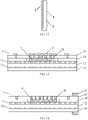
- the stacking substrateincludes: a stacking chip substrate, circuit wiring, a laminated sheet, a stacking chip, external wiring, a solder pad, a lower surface substrate, and an upper surface substrate provided with a plurality of connection holes, where the circuit wiring is disposed on an upper surface and a lower surface of the stacking chip substrate; the stacking chip is disposed on the upper surface of the stacking chip substrate and is connected to the circuit wiring; the laminated sheet is disposed on the circuit wiring on the upper surface of the stacking chip substrate; the upper surface substrate is disposed on the stacking chip and the laminated sheet; the lower surface substrate is disposed below the circuit wiring on the lower surface of the stacking chip substrate; positions of the plurality of connection holes correspond to a position of an input/output interface of the stacking chip; a conductive medium is disposed in the connection holes, and the conductive medium is connected to the input/output interface of the stacking chip; wiling, the solder pad is disposed at a bottom end of an outer side face of the upper surface substrate, and
- the side edge of the stacking substrateis disposed on the main substrate, thereby achieving high-density stacking of chips; and the stacking chip is connected to the main chip by disposing the side edge of the stacking substrate on the main substrate, so that the stacking substrate functions like a radiating tooth in a metal radiator.
- the stacking substratefunctions like a radiating tooth in a metal radiator.
- the present inventionis directed to a chip packaging structure according to claim 1. As shown in FIG. 1 , the structure includes:
- the side edge of the stacking substrate 2is disposed on the main substrate 1.
- This structureis similar to the structure of a metal radiator, and the stacking substrate 2 functions as a radiating tooth in the metal radiator.
- the stacking substrate 2is disposed on the main substrate 1 perpendicularly.
- the side edge of the stacking substrateis disposed on the main substrate, thereby achieving high-density stacking of chips; and such a configuration enables the stacking substrate to function like a radiating tooth in a metal radiator.
- heat of the chipscan be quickly taken away, and thermal interference between the chips (between the stacking chip and the main chip or between the stacking chips) is avoided, thereby effectively achieving efficient heat dissipation of the stacked chips.
- the side edge of the stacking substrateis disposed on the main substrate, a length of wiring between the stacking chip and the main chip is greatly reduced compared with the prior art, thereby improving electrical performance of the chip packaging structure.
- the stacking substrate 2is disposed on the main substrate 1 perpendicularly, so that the stacking chip is connected to the main chip vertically, thereby achieving high-density stacking of chips and further improving the heat dissipation efficiency.
- the chip stacking packaging structurecan include: a plurality of stacking substrates 2, and the plurality of stacking substrates 2 is spaced from each other.
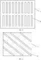
- the stacking substrates 2may be disposed on the main substrate 1 vertically according to various layouts. For example, as shown in FIG. 2 , the stacking substrates 2 may be arranged in one row and disposed in parallel on the main substrate 1. This embodiment is not an embodiment of the invention but helpful to understand certain aspects thereof.; as shown in FIG. 3 , the stacking substrates 2 may be arranged in two rows and disposed on the main substrate 1, and stacking substrates 2 in each row are parallel to each other. This embodiment is not an embodiment of the invention but helpful to understand certain aspects thereof.; and as shown in FIG.
- the stacking substrates 2may be disposed in parallel on the main substrate 1 along a diagonal of the main substrate 1.
- This embodimentis not an embodiment of the invention but helpful to understand certain aspects thereof..
- the layout of the stacking substratesis not limited to the foregoing three manners, and a specific layout manner of the stacking substrates on the main substrate is not limited herein.
- the chip stacking packaging structurecan include: at least one heat radiating fin 6, where the heat radiating fin 6 is disposed on the main substrate 1, and the heat radiating fin and the stacking substrate 2 are spaced from each other.
- the heat radiating finmay also be disposed on the main substrate perpendicularly, so as to ensure that the heat radiating fin and the stacking substrate can be spaced from each other.
- the heat radiating fin 6 and the stacking substrate 2may be disposed on the main substrate in a mixed manner, and the heat radiating fin 6 functions like a radiating tooth in a metal radiator, thereby further facilitating heat dissipation of the chip stacking packaging structure.
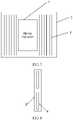
- the chip stacking packaging structurecan include: a metal radiator 7, where the metal radiator 7 is disposed on the main substrate 1 and corresponds to a position at which the main chip is disposed, and the metal radiator 7 and the stacking substrate 2 are spaced from each other.
- FIG. 7is not an embodiment of the invention but helpful to understand certain aspects thereof.
- a certain space for installing the metal radiator 7may be reserved in a central area of the main substrate 1, and the stacking substrates 2 are disposed surrounding the metal radiator. In this way, heat dissipation of the stacking chip and the main chip can be achieved more effectively.
- the metal radiator 7may be disposed on the main substrate 1 vertically according to various layouts. For example, as shown in FIG. 6 , the metal radiator 7 may be disposed in the central area of the main substrate 1, and the stacking substrates 2 may be arranged in two rows and disposed on two sides of the metal radiator 7; or as shown in FIG 7 , the stacking substrates 2 may be arranged in one row and disposed on two sides of the metal radiator 7.
- the stacking chipis disposed on a surface of the stacking substrate or inside the stacking substrate. As shown in FIG. 8 , the stacking chip 4 may be buried inside the stacking substrate 2, or as shown in FIG. 9 , the stacking chip 4 may be surface-mounted to the stacking substrate 2. These embodiments are not an embodiment of the invention but helpful to understand certain aspects thereof.
- the main chipis disposed on a surface of the main substrate or inside the main substrate. As shown in FIG. 10 , the main chip 3 may be surface-mounted to the main substrate 1. This embodiment is not an embodiment of the invention but helpful to understand certain aspects thereof. If the main chip 3 is disposed on the surface of the main substrate 1, the central area (that is, the area where the main chip is located) of the main substrate may be used not for disposing the stacking substrate but for disposing a metal radiator, or the stacking substrate 2 is disposed in the central area of the main substrate 1 in a bridging manner, that is, an area 21, which is located above the main chip, of the stacking substrate 2 is not connected to the main substrate 1, and an area 22, which extends beyond the main chip, of the stacking substrate 2 is connected to the main substrate 1.
- One surface or two surfaces of the stacking substrate and the heat radiating finare covered with a copper foil. Covering a surface with a copper foil further improves the heat dissipation capability of the stacking substrate and the heat radiating fin. As shown in FIG. 11 , both surfaces of the stacking substrate 2 may be covered with a copper foil. This embodiment is not an embodiment of the invention but helpful to understand certain aspects thereof. As shown in FIG. 12 , one surface of the stacking substrate 2 may be covered with a copper foil 5, and the stacking chip 4 is disposed on the other surface of the stacking substrate. This embodiment is not an embodiment of the invention but helpful to understand certain aspects thereof.
- the main substrate 1includes: a main chip substrate 12, circuit wiring 11, a laminated sheet 18, a main chip 3, a chip connection area 17, a lower surface substrate 19, and an upper surface substrate 15 provided with a plurality of connection holes 16.
- the circuit wiring 11is disposed on an upper surface and a lower surface of the main chip substrate 12.
- the circuit wiring 11may be of multiple layers, where the multiple layers of circuit wiring are spaced from each other by the laminated sheet, and the laminated sheet may be a prepreg.
- the main chip 3is disposed on the upper surface of the main chip substrate 12 and is connected to the circuit wiring 11.
- the laminated sheet 18is disposed on the circuit wiring 11 on the upper surface of the main chip substrate 12.
- the upper surface substrate 15is disposed on the main chip 3 and the laminated sheet 18.
- the lower surface substrate 19is disposed below the circuit wiring on the lower surface of the main chip substrate 12.
- Positions of the plurality of connection holes 16correspond to a position of an input/output interface of the main chip 3.
- a conductive mediumis disposed in the connection holes 16, and the conductive medium is connected to the input/output interface of the main chip 3.
- the chip connection area 17covers openings at one side of the connection holes 16 that is distant from the main chip 3, and is connected to the conductive medium, that is, the chip connection area 17 is connected to the input/output interface of the main chip 3 or the circuit wiring 11 through the connection holes 16.
- the chip connection area 17is used to connect the stacking substrate.
- the stacking substrate 2includes: a stacking chip substrate 22, circuit wiring 21, a laminated sheet 28, a stacking chip 4, external wiring, a solder pad 27, a lower surface substrate 29, and an upper surface substrate 25 provided with a plurality of connection holes 26.
- the circuit wiring 21is disposed on an upper surface and a lower surface of the stacking chip substrate 22.
- the circuit wiring 21may be of multiple layers, where the multiple layers of circuit wiring are spaced from each other by the laminated sheet, and the laminated sheet may be a prepreg.
- the stacking chip 4is disposed on the upper surface of the stacking chip substrate 22 and is connected to the circuit wiring 21.
- the laminated sheet 28is disposed on the circuit wiring 21 on the upper surface of the stacking chip substrate 22.
- the upper surface substrate 25is disposed on the stacking chip 4 and the laminated sheet 28.
- the lower surface substrate 29is disposed below the circuit wiring 21 on the lower surface of the stacking chip substrate 22.
- Positions of the plurality of connection holes 26correspond to a position of an input/output interface of the stacking chip 4.
- a conductive mediumis disposed in the connection holes 26, and the conductive medium is connected to the input/output interface of the stacking chip. 4.
- the solder pad 27is disposed at a bottom end (the right side in the figure) of an outer side face (that is, a side distant from the stacking chip and the circuit wiring) of the upper surface substrate 25, and the solder pad 27 is used to connect the main substrate.
- the external wiringis disposed on the outer side face of the upper surface substrate 25, and two ends of the external wiring are connected to the solder pad and the conductive medium separately, that is, the solder pad 27 is connected to the input/output interface of the stacking chip 4 and the circuit wiring 21 through the external wiring and the connection holes 26.
- the stacking substrateis disposed on the main substrate perpendicularly, thereby achieving high-density stacking of chips; and the stacking chip is connected to the main chip vertically, so that the stacking substrate functions like a radiating tooth in a metal radiator.
- the stacking substratefunctions like a radiating tooth in a metal radiator.
Landscapes
- Engineering & Computer Science (AREA)
- Microelectronics & Electronic Packaging (AREA)
- Power Engineering (AREA)
- Computer Hardware Design (AREA)
- Physics & Mathematics (AREA)
- Condensed Matter Physics & Semiconductors (AREA)
- General Physics & Mathematics (AREA)
- Manufacturing & Machinery (AREA)
- Chemical & Material Sciences (AREA)
- Materials Engineering (AREA)
- Cooling Or The Like Of Semiconductors Or Solid State Devices (AREA)
- Cooling Or The Like Of Electrical Apparatus (AREA)
Description
- The present invention relates to the field of chip packaging technologies, and in particular, to a chip stacking packaging structure.
- To meet a requirement for high density and miniaturization of integrated circuits, chip stacking has become a development trend of integrated circuits. In the prior art, a chip stacking manner is generally: placing a chip horizontally, and stacking one or more chips on the chip vertically upward layer by layer. The chips may be connected to each other by means of laser drilling, that is, holes are formed in the stacked chips by using a laser, and then the chips are connected to each other by electroplating.
- For a chip stacking packaging structure in the prior art, since chips are closely stacked horizontally, such a stacking manner leads to low heat dissipation performance of the chips. Heat generated by the chips can only be conducted to the outside through metal wiring and a material of chips themselves, resulting in a low heat conduction efficiency. In addition, since a high-power chip and a low-power chip are stacked together, the temperature of the low-power chip increases under influence of the high-power chip, thereby affecting performance of the chip. US patent
US 5,530,623 discusses a memory packaging scheme including several memory module sockets mounted to a printed circuit board and interconnected by a common set of address, data and control transmission lines within the printed circuit board. The transmission lines are interrupted at each connector. Cooperating memory modules are installed in sequence into one or more of the module sockets. Installation of a memory module into a memory socket closes the open circuits for each one of the transmission lines at the memory socket, extending the uninterrupted length of the transmission lines to the next memory socket in the sequence. US published patent applicationUS 2007/181988 A1 discusses a PCB having an embedded bare chip and a manufacturing method thereof. The method of manufacturing a PCB may include embedding a bare chip in a board such that electrode pads of the bare chip are exposed, and forming electrode bumps on the electrode pads. - A technical issue to be solved by the present invention is to provide a chip stacking packaging structure, so as to achieve high-density stacking of chips, and improve a heat dissipation efficiency of the chip stacking packaging structure. The invention is set out in the appended set of claims.
- According to the present invention, the chip packaging structure comprises all features of
claim 1 and includes: - a main substrate and at least one stacking substrate, where a main chip is disposed in the main substrate, and at least one stacking chip is disposed inside the stacking substrate; wherein the main substrate comprises: a main chip substrate, circuit wiring, a laminated sheet, a chip connection area and an upper surface substrate provided with a plurality of connection holes, wherein the circuit wiring is disposed on an upper surface and a lower surface of the main chip substrate; the main chip is disposed on the upper surface of the main chip substrate and is connected to the circuit wiring; the laminated sheet is disposed on the circuit wiring on the upper surface of the main chip substrate; the upper surface substrate is disposed on the main chip and the laminated sheet; positions of the plurality of connection holes correspond to a position of an input/output interface of the main chip;
- a conductive medium is disposed in the connection holes, and the conductive medium is connected to the input/output interface of the main chip;
- the chip connection area covers openings at one side of the connection holes that is distant from the main chip, and is connected to the conductive medium; and the chip connection area is used to connect the stacking substrate and wherein the stacking substrate comprises a solder pad disposed at an end of an outer side face of the upper surface substrate and extending to the side edge of the upper surface substrate and connecting to the stacking chip;
- the side edge of the stacking substrate is disposed on the main substrate, so that the stacking chip is connected to the main chip.
- According to the present invention, the stacking substrate is disposed on the main substrate perpendicularly.
- In a preferred implementation of the present invention the at least one stacking substrate includes: a plurality of stacking substrates, and the plurality of stacking substrates is spaced from each other.
- In a further preferred implementation of the present invention the chip stacking packaging structure further includes: at least one heat radiating fin, where the heat radiating fin is disposed on the main substrate, and the heat radiating fin and the stacking substrate are spaced from each other.
- In a further preferred implementation of the present invention the chip stacking packaging structure further includes: a metal radiator, where the metal radiator is disposed on the main substrate and corresponds to a position at which the main chip is disposed, and the metal radiator and the stacking substrate are spaced from each other.
- In a further preferred implementation of the present invention one surface or two surfaces of the stacking substrate are covered with a copper foil.
- The stacking substrate includes: a stacking chip substrate, circuit wiring, a laminated sheet, a stacking chip, external wiring, a solder pad, a lower surface substrate, and an upper surface substrate provided with a plurality of connection holes, where the circuit wiring is disposed on an upper surface and a lower surface of the stacking chip substrate; the stacking chip is disposed on the upper surface of the stacking chip substrate and is connected to the circuit wiring; the laminated sheet is disposed on the circuit wiring on the upper surface of the stacking chip substrate; the upper surface substrate is disposed on the stacking chip and the laminated sheet; the lower surface substrate is disposed below the circuit wiring on the lower surface of the stacking chip substrate; positions of the plurality of connection holes correspond to a position of an input/output interface of the stacking chip; a conductive medium is disposed in the connection holes, and the conductive medium is connected to the input/output interface of the stacking chip; wiling, the solder pad is disposed at a bottom end of an outer side face of the upper surface substrate, and the solder pad is used to connect the main substrate; and the external wiring is disposed on the outer side face of the upper surface substrate, and two ends of the external wiring are connected to the solder pad and the conductive medium separately.
- In the chip stacking packaging structure provided by embodiments of the present invention, the side edge of the stacking substrate is disposed on the main substrate, thereby achieving high-density stacking of chips; and the stacking chip is connected to the main chip by disposing the side edge of the stacking substrate on the main substrate, so that the stacking substrate functions like a radiating tooth in a metal radiator. In this way, in a case of forced air cooling, heat of the chips can be quickly taken away, and thermal interference between the chips is avoided, thereby effectively achieving efficient heat dissipation of the stacked chips. In addition, since the stacking substrate is disposed on the main substrate vertically, a length of wiring between the stacking chip and the main chip is greatly reduced compared with the prior art, thereby improving electrical performance of the chip packaging structure.
- To describe the technical solutions in the embodiments of the present invention or in the prior art more clearly, the following briefly introduces the accompanying drawings required for describing the embodiments.
FIG. 1 is a schematic diagram of a chip stacking packaging structure provided by an embodiment of the present invention;FIG. 2 is a schematic diagram where stacking substrates are arranged in one row and disposed in parallel on a main substrate. This embodiment is not an embodiment of the invention but helpful to understand certain aspects thereof;FIG. 3 is a schematic diagram where stacking substrates are arranged in two rows and disposed in parallel on a main substrate. This embodiment is not an embodiment of the invention but helpful to understand certain aspects thereof;FIG. 4 is a schematic diagram where stacking substrates are disposed in parallel on a main substrate along a diagonal of the main substrate. This embodiment is not an embodiment of the invention but helpful to understand certain aspects thereof;FIG. 5 is a schematic diagram where a heat radiating fin is disposed on the main substrate according to an embodiment of the present invention;FIG. 6 is a schematic diagram where a metal radiator is disposed on the main substrate according to an embodiment of the present invention;FIG. 7 is a schematic diagram where stacking substrates are arranged in one row and disposed on two sides of a metal radiator. This embodiment is not an embodiment of the invention but helpful to understand certain aspects thereof;FIG. 8 is a schematic diagram where a stacking chip is disposed inside a stacking substrate. This embodiment is not an embodiment of the invention but helpful to understand certain aspects thereof;FIG. 9 is a schematic diagram where a stacking chip is disposed on a surface of a stacking substrate. This embodiment is not an embodiment of the invention but helpful to understand certain aspects thereof;FIG. 10 is a schematic diagram where a main chip is disposed on a surface of a main substrate. This embodiment is not an embodiment of the invention but helpful to understand certain aspects thereof;FIG 11 is a schematic diagram where two surfaces of a stacking substrate are provided with a copper foil. This embodiment is not an embodiment of the invention but helpful to understand certain aspects thereof;FIG. 12 is a schematic diagram where one surface of a stacking substrate is covered with a copper foil. This embodiment is not an embodiment of the invention but helpful to understand certain aspects thereof;FIG. 13 is a schematic structural diagram of a main/stacking substrate implemented in a chip packaging structure according to the present invention; andFIG. 14 is a schematic structural diagram of a main/stacking substrate implemented in a chip packaging structure according to the present invention.- The following clearly and completely describes the technical solutions with reference to the accompanying drawings.
- The present invention is directed to a chip packaging structure according to
claim 1. As shown inFIG. 1 , the structure includes: - a
main substrate 1 and at least onestacking substrate 2, where amain chip 3 is disposed in themain substrate 1, and at least onestacking chip 4 is disposed inside thestacking substrate 2; and - a side edge of the
stacking substrate 2 is disposed on themain substrate 1, so that thestacking chip 4 is connected to themain chip 3. - The side edge of the
stacking substrate 2 is disposed on themain substrate 1. This structure is similar to the structure of a metal radiator, and thestacking substrate 2 functions as a radiating tooth in the metal radiator. The stackingsubstrate 2 is disposed on themain substrate 1 perpendicularly. - In the chip stacking packaging structure, the side edge of the stacking substrate is disposed on the main substrate, thereby achieving high-density stacking of chips; and such a configuration enables the stacking substrate to function like a radiating tooth in a metal radiator. In this way, in a case of forced air cooling, heat of the chips can be quickly taken away, and thermal interference between the chips (between the stacking chip and the main chip or between the stacking chips) is avoided, thereby effectively achieving efficient heat dissipation of the stacked chips. In addition, since the side edge of the stacking substrate is disposed on the main substrate, a length of wiring between the stacking chip and the main chip is greatly reduced compared with the prior art, thereby improving electrical performance of the chip packaging structure.
- In the present invention, as shown in
FIG. 1 , the stackingsubstrate 2 is disposed on themain substrate 1 perpendicularly, so that the stacking chip is connected to the main chip vertically, thereby achieving high-density stacking of chips and further improving the heat dissipation efficiency. - Further, the chip stacking packaging structure can include: a plurality of stacking
substrates 2, and the plurality of stackingsubstrates 2 is spaced from each other. The stackingsubstrates 2 may be disposed on themain substrate 1 vertically according to various layouts. For example, as shown inFIG. 2 , the stackingsubstrates 2 may be arranged in one row and disposed in parallel on themain substrate 1. This embodiment is not an embodiment of the invention but helpful to understand certain aspects thereof.; as shown inFIG. 3 , the stackingsubstrates 2 may be arranged in two rows and disposed on themain substrate 1, and stackingsubstrates 2 in each row are parallel to each other. This embodiment is not an embodiment of the invention but helpful to understand certain aspects thereof.; and as shown inFIG. 4 , the stackingsubstrates 2 may be disposed in parallel on themain substrate 1 along a diagonal of themain substrate 1. This embodiment is not an embodiment of the invention but helpful to understand certain aspects thereof.. In the embodiment of the present invention, the layout of the stacking substrates is not limited to the foregoing three manners, and a specific layout manner of the stacking substrates on the main substrate is not limited herein. - Further, as shown in
FIG. 5 , the chip stacking packaging structure can include: at least oneheat radiating fin 6, where theheat radiating fin 6 is disposed on themain substrate 1, and the heat radiating fin and the stackingsubstrate 2 are spaced from each other. When the stacking substrate is disposed perpendicularly, the heat radiating fin may also be disposed on the main substrate perpendicularly, so as to ensure that the heat radiating fin and the stacking substrate can be spaced from each other. - The
heat radiating fin 6 and the stackingsubstrate 2 may be disposed on the main substrate in a mixed manner, and theheat radiating fin 6 functions like a radiating tooth in a metal radiator, thereby further facilitating heat dissipation of the chip stacking packaging structure. - Further, as shown in
FIG. 6 andFIG. 7 , the chip stacking packaging structure can include: ametal radiator 7, where themetal radiator 7 is disposed on themain substrate 1 and corresponds to a position at which the main chip is disposed, and themetal radiator 7 and the stackingsubstrate 2 are spaced from each other.FIG. 7 is not an embodiment of the invention but helpful to understand certain aspects thereof. - A certain space for installing the
metal radiator 7 may be reserved in a central area of themain substrate 1, and the stackingsubstrates 2 are disposed surrounding the metal radiator. In this way, heat dissipation of the stacking chip and the main chip can be achieved more effectively. Themetal radiator 7 may be disposed on themain substrate 1 vertically according to various layouts. For example, as shown inFIG. 6 , themetal radiator 7 may be disposed in the central area of themain substrate 1, and the stackingsubstrates 2 may be arranged in two rows and disposed on two sides of themetal radiator 7; or as shown inFIG 7 , the stackingsubstrates 2 may be arranged in one row and disposed on two sides of themetal radiator 7. - Further, the stacking chip is disposed on a surface of the stacking substrate or inside the stacking substrate. As shown in
FIG. 8 , the stackingchip 4 may be buried inside the stackingsubstrate 2, or as shown inFIG. 9 , the stackingchip 4 may be surface-mounted to the stackingsubstrate 2. These embodiments are not an embodiment of the invention but helpful to understand certain aspects thereof. - The main chip is disposed on a surface of the main substrate or inside the main substrate. As shown in
FIG. 10 , themain chip 3 may be surface-mounted to themain substrate 1. This embodiment is not an embodiment of the invention but helpful to understand certain aspects thereof. If themain chip 3 is disposed on the surface of themain substrate 1, the central area (that is, the area where the main chip is located) of the main substrate may be used not for disposing the stacking substrate but for disposing a metal radiator, or the stackingsubstrate 2 is disposed in the central area of themain substrate 1 in a bridging manner, that is, anarea 21, which is located above the main chip, of the stackingsubstrate 2 is not connected to themain substrate 1, and anarea 22, which extends beyond the main chip, of the stackingsubstrate 2 is connected to themain substrate 1. - One surface or two surfaces of the stacking substrate and the heat radiating fin are covered with a copper foil. Covering a surface with a copper foil further improves the heat dissipation capability of the stacking substrate and the heat radiating fin. As shown in
FIG. 11 , both surfaces of the stackingsubstrate 2 may be covered with a copper foil. This embodiment is not an embodiment of the invention but helpful to understand certain aspects thereof. As shown inFIG. 12 , one surface of the stackingsubstrate 2 may be covered with acopper foil 5, and the stackingchip 4 is disposed on the other surface of the stacking substrate. This embodiment is not an embodiment of the invention but helpful to understand certain aspects thereof. - Further, in a main/stacking substrate implemented in a chip packaging structure according to the present invention, as shown in
FIG. 13 , themain substrate 1 includes: amain chip substrate 12,circuit wiring 11, alaminated sheet 18, amain chip 3, achip connection area 17, alower surface substrate 19, and anupper surface substrate 15 provided with a plurality of connection holes 16. Thecircuit wiring 11 is disposed on an upper surface and a lower surface of themain chip substrate 12. Thecircuit wiring 11 may be of multiple layers, where the multiple layers of circuit wiring are spaced from each other by the laminated sheet, and the laminated sheet may be a prepreg. Themain chip 3 is disposed on the upper surface of themain chip substrate 12 and is connected to thecircuit wiring 11. Thelaminated sheet 18 is disposed on thecircuit wiring 11 on the upper surface of themain chip substrate 12. Theupper surface substrate 15 is disposed on themain chip 3 and thelaminated sheet 18. Thelower surface substrate 19 is disposed below the circuit wiring on the lower surface of themain chip substrate 12. Positions of the plurality of connection holes 16 correspond to a position of an input/output interface of themain chip 3. A conductive medium is disposed in the connection holes 16, and the conductive medium is connected to the input/output interface of themain chip 3. Thechip connection area 17 covers openings at one side of the connection holes 16 that is distant from themain chip 3, and is connected to the conductive medium, that is, thechip connection area 17 is connected to the input/output interface of themain chip 3 or thecircuit wiring 11 through the connection holes 16. Thechip connection area 17 is used to connect the stacking substrate. - As shown in
FIG. 14 , the stackingsubstrate 2 includes: a stackingchip substrate 22,circuit wiring 21, alaminated sheet 28, a stackingchip 4, external wiring, asolder pad 27, alower surface substrate 29, and anupper surface substrate 25 provided with a plurality of connection holes 26. Thecircuit wiring 21 is disposed on an upper surface and a lower surface of the stackingchip substrate 22. Thecircuit wiring 21 may be of multiple layers, where the multiple layers of circuit wiring are spaced from each other by the laminated sheet, and the laminated sheet may be a prepreg. The stackingchip 4 is disposed on the upper surface of the stackingchip substrate 22 and is connected to thecircuit wiring 21. Thelaminated sheet 28 is disposed on thecircuit wiring 21 on the upper surface of the stackingchip substrate 22. Theupper surface substrate 25 is disposed on the stackingchip 4 and thelaminated sheet 28. Thelower surface substrate 29 is disposed below thecircuit wiring 21 on the lower surface of the stackingchip substrate 22. Positions of the plurality of connection holes 26 correspond to a position of an input/output interface of the stackingchip 4. A conductive medium is disposed in the connection holes 26, and the conductive medium is connected to the input/output interface of the stacking chip. 4. Thesolder pad 27 is disposed at a bottom end (the right side in the figure) of an outer side face (that is, a side distant from the stacking chip and the circuit wiring) of theupper surface substrate 25, and thesolder pad 27 is used to connect the main substrate. The external wiring is disposed on the outer side face of theupper surface substrate 25, and two ends of the external wiring are connected to the solder pad and the conductive medium separately, that is, thesolder pad 27 is connected to the input/output interface of the stackingchip 4 and thecircuit wiring 21 through the external wiring and the connection holes 26. - In the chip stacking packaging structure provided by the present invention, the stacking substrate is disposed on the main substrate perpendicularly, thereby achieving high-density stacking of chips; and the stacking chip is connected to the main chip vertically, so that the stacking substrate functions like a radiating tooth in a metal radiator. In this way, in a case of forced air cooling, heat of the chips can be quickly taken away, and thermal interference between the chips is avoided. Since the heat radiating fin or the metal radiator dedicated for heat dissipation is disposed on the main substrate, efficient heat dissipation of the stacked chips can be achieved effectively. In addition, since the stacking substrate is disposed on the main substrate vertically, a length of wiring between the stacking chip and the main chip is greatly reduced compared with the prior art, thereby improving electrical performance of the chip packaging structure.
Claims (5)
- A chip packaging structure, comprising: a main substrate (1) and at least one stacking substrate (2), wherein a main chip (3) is disposed in the main substrate (1), and at least one stacking chip (4) is disposed inside the stacking substrate (2);wherein the main substrate (1) comprises: a main chip substrate (12), first circuit wiring (11), a first laminated sheet (18), a chip connection area (17), a first lower surface substrate (19), and a first upper surface substrate (15) provided with a plurality of first connection holes (16), wherein the first circuit wiring (11) is disposed on an upper surface and a lower surface of the main chip substrate (12); the main chip (3) is disposed on the upper surface of the main chip substrate (12) and is connected to the first circuit wiring (11); the first laminated sheet (18) is disposed on the first circuit wiring (11) on the upper surface of the main chip substrate (12); the first upper surface substrate (15) is disposed on the main chip (3) and the first laminated sheet (18); the first lower surface substrate (19) is disposed below the first circuit wiring (11) on the lower surface of the main chip substrate (12); positions of the plurality of first connection holes (16) correspond to a position of an input/output interface of the main chip (3); a first conductive medium is disposed in the first connection holes (16), and the first conductive medium is connected to the input/output interface of the main chip (3); the chip connection area (17) covers openings at one side of the first connection holes (16) that is distant from the main chip (3), and is connected to the first conductive medium; and the chip connection area (17) is used to connect the stacking substrate (2) andwherein the stacking substrate (2) comprises a solder pad (27) disposed at an end of an outer side face of a second upper surface substrate (25) and extending to the side edge of the second upper surface substrate (25) and connecting to a stacking chip (4), a stacking chip substrate (22), second circuit wiring (21), a second laminated sheet (28), the stacking chip (4), external wiring, a second lower surface substrate (29), and the second upper surface substrate (25) provided with a plurality of second connection holes (26), wherein the second circuit wiring (21) is disposed on an upper surface and a lower surface of the stacking chip substrate (22); the stacking chip (4) is disposed on the upper surface of the stacking chip substrate (22) and is connected to the second circuit wiring (21); the second laminated sheet (28) is disposed on the second circuit wiring (21) on the upper surface of the stacking chip substrate (22); the second upper surface substrate (25) is disposed on the stacking chip (4) and the second laminated sheet (28); the second lower surface substrate (29) is disposed below the second circuit wiring (21) on the lower surface of the stacking chip substrate (22); positions of the plurality of second connection holes (26) correspond to a position of an input/output interface of the stacking chip (4) and; a second conductive medium is disposed in the second connection holes (26), and the second conductive medium is connected to the input/output interface of the stacking chip (4); the solder pad (27) is disposed at a bottom end of an outer side face of the second upper surface substrate (25), and the solder pad (27) is used to connect the main substrate (1); the stacking substrate (2) is disposed on the main substrate (1) perpendicularly; and the external wiring is disposed on the outer side face of the second upper surface substrate (25), and two ends of the external wiring are connected to the solder pad and the second conductive medium separately;whereby a side edge of the stacking substrate (2) is disposed on the main substrate (1), so that the stacking chip (4) is connected to the main chip (3).
- The structure according to claim 1 , wherein the at least one stacking substrate (2) comprises: a plurality of stacking substrates (2), and the plurality of stacking substrates (2) is spaced from each other.
- The structure according to claim 2, wherein the structure further comprises: at least one heat radiating fin (6), the heat radiating fin (6) is disposed on the main substrate (1), and the heat radiating fin (6) and the stacking substrate (2) are spaced from each other.
- The structure according to claim 3, further comprising: a metal radiator (7), wherein the metal radiator (7) is disposed on the main substrate (1) and corresponds to a position at which the main chip (3) is disposed, and the metal radiator (7) and the stacking substrate (2) are spaced from each other.
- The structure according to any one of claims 1 to 4, wherein one surface or two surfaces of the stacking substrate (2) are covered with a copper foil (5).
Applications Claiming Priority (2)
| Application Number | Priority Date | Filing Date | Title |
|---|---|---|---|
| CN201210165554.8ACN102693968B (en) | 2012-05-25 | 2012-05-25 | Chip stacking and packaging structure |
| PCT/CN2012/083609WO2013174099A1 (en) | 2012-05-25 | 2012-10-26 | Chip stack encapsulation structure |
Publications (3)
| Publication Number | Publication Date |
|---|---|
| EP2819163A1 EP2819163A1 (en) | 2014-12-31 |
| EP2819163A4 EP2819163A4 (en) | 2015-02-25 |
| EP2819163B1true EP2819163B1 (en) | 2023-01-11 |
Family
ID=46859324
Family Applications (1)
| Application Number | Title | Priority Date | Filing Date |
|---|---|---|---|
| EP12877457.7AActiveEP2819163B1 (en) | 2012-05-25 | 2012-10-26 | Chip stack structure |
Country Status (4)
| Country | Link |
|---|---|
| US (1) | US9257358B2 (en) |
| EP (1) | EP2819163B1 (en) |
| CN (1) | CN102693968B (en) |
| WO (1) | WO2013174099A1 (en) |
Families Citing this family (4)
| Publication number | Priority date | Publication date | Assignee | Title |
|---|---|---|---|---|
| CN102693968B (en) | 2012-05-25 | 2014-12-03 | 华为技术有限公司 | Chip stacking and packaging structure |
| CN108352371A (en)* | 2015-11-20 | 2018-07-31 | 捷恩智株式会社 | The manufacturing method of radiator, e-machine, lighting machine and radiator |
| US11276641B1 (en)* | 2020-01-06 | 2022-03-15 | Rockwell Collins, Inc. | Conformal multi-plane material deposition |
| WO2022016470A1 (en)* | 2020-07-23 | 2022-01-27 | 华为技术有限公司 | Chip encapsulation structure and electronic device |
Family Cites Families (17)
| Publication number | Priority date | Publication date | Assignee | Title |
|---|---|---|---|---|
| US4266282A (en)* | 1979-03-12 | 1981-05-05 | International Business Machines Corporation | Vertical semiconductor integrated circuit chip packaging |
| US5362986A (en)* | 1993-08-19 | 1994-11-08 | International Business Machines Corporation | Vertical chip mount memory package with packaging substrate and memory chip pairs |
| US5530623A (en)* | 1993-11-19 | 1996-06-25 | Ncr Corporation | High speed memory packaging scheme |
| US6075287A (en)* | 1997-04-03 | 2000-06-13 | International Business Machines Corporation | Integrated, multi-chip, thermally conductive packaging device and methodology |
| US6535387B2 (en)* | 2001-06-28 | 2003-03-18 | Intel Corporation | Heat transfer apparatus |
| JP2004281920A (en)* | 2003-03-18 | 2004-10-07 | Seiko Epson Corp | Semiconductor device, electronic device, electronic equipment, method of manufacturing semiconductor device, and method of manufacturing electronic device |
| AU2005228442A1 (en)* | 2004-03-29 | 2005-10-13 | Cytomatrix, Llc | Methods for production of regulatory T cells and uses thereof |
| US7522421B2 (en)* | 2004-09-03 | 2009-04-21 | Entorian Technologies, Lp | Split core circuit module |
| US20060221573A1 (en)* | 2005-04-04 | 2006-10-05 | Ming Li | Heat sink for multiple semiconductor modules |
| US8081474B1 (en)* | 2007-12-18 | 2011-12-20 | Google Inc. | Embossed heat spreader |
| KR100736635B1 (en)* | 2006-02-09 | 2007-07-06 | 삼성전기주식회사 | Bare chip embedded printed circuit board and manufacturing method thereof |
| TWI307946B (en) | 2006-05-24 | 2009-03-21 | Phoenix Prec Technology Corp | Stack structure of circuit board having embedded with semicondutor component |
| US20090114261A1 (en)* | 2007-08-29 | 2009-05-07 | Robert Stancel | Edge Mountable Electrical Connection Assembly |
| US20090166065A1 (en)* | 2008-01-02 | 2009-07-02 | Clayton James E | Thin multi-chip flex module |
| CN101604685A (en)* | 2008-06-11 | 2009-12-16 | 英业达股份有限公司 | Memory module |
| US8298914B2 (en) | 2008-08-19 | 2012-10-30 | International Business Machines Corporation | 3D integrated circuit device fabrication using interface wafer as permanent carrier |
| CN102693968B (en)* | 2012-05-25 | 2014-12-03 | 华为技术有限公司 | Chip stacking and packaging structure |
- 2012
- 2012-05-25CNCN201210165554.8Apatent/CN102693968B/ennot_activeExpired - Fee Related
- 2012-10-26WOPCT/CN2012/083609patent/WO2013174099A1/enactiveApplication Filing
- 2012-10-26EPEP12877457.7Apatent/EP2819163B1/enactiveActive
- 2014
- 2014-11-25USUS14/552,674patent/US9257358B2/enactiveActive
Also Published As
| Publication number | Publication date |
|---|---|
| CN102693968B (en) | 2014-12-03 |
| US20150076686A1 (en) | 2015-03-19 |
| US9257358B2 (en) | 2016-02-09 |
| EP2819163A1 (en) | 2014-12-31 |
| WO2013174099A1 (en) | 2013-11-28 |
| CN102693968A (en) | 2012-09-26 |
| EP2819163A4 (en) | 2015-02-25 |
Similar Documents
| Publication | Publication Date | Title |
|---|---|---|
| US8971045B1 (en) | Module having at least one thermally conductive layer between printed circuit boards | |
| EP2986088B1 (en) | Printed circuit board, manufacturing method thereof and radio-frequency device | |
| CN104900634A (en) | Package structure and stacked package module with same | |
| CN104900609A (en) | Package structure | |
| US9318407B2 (en) | Pop package structure | |
| CN104284533A (en) | Multilayer circuit board, manufacturing method thereof, and communication device | |
| US10734317B2 (en) | Discrete electronic device embedded in chip module | |
| CN204243028U (en) | Electronic system | |
| EP2819163B1 (en) | Chip stack structure | |
| US20090161318A1 (en) | Thermal management systems and methods | |
| KR20160038304A (en) | Circuit board | |
| CN112185911A (en) | Semiconductor assembly including vertical integrated circuit and method of manufacturing the same | |
| US11096290B2 (en) | Printed circuit board with edge soldering for high-density packages and assemblies | |
| CN212660367U (en) | PCB structure for optimizing heat dissipation performance of power chip | |
| EP3533303B1 (en) | Power module | |
| CN110062555B (en) | Heat radiation module and optical module | |
| CN102122879B (en) | Laminated power supply and interconnecting method for laminated power supplies | |
| CN214205971U (en) | Printed circuit board with embedded power device | |
| CN220439616U (en) | Power device module and driver | |
| CN210432028U (en) | Printed circuit board with double-layer structure | |
| CN209562910U (en) | Circuit board and supercomputing equipment | |
| WO2018157314A1 (en) | Photoelectric hybrid package assembly | |
| EP4124182A1 (en) | Circuit board and preparation method therefor | |
| JP2013084658A (en) | Wiring board for mounting semiconductor element and semiconductor device using the same |
Legal Events
| Date | Code | Title | Description |
|---|---|---|---|
| PUAI | Public reference made under article 153(3) epc to a published international application that has entered the european phase | Free format text:ORIGINAL CODE: 0009012 | |
| 17P | Request for examination filed | Effective date:20140923 | |
| AK | Designated contracting states | Kind code of ref document:A1 Designated state(s):AL AT BE BG CH CY CZ DE DK EE ES FI FR GB GR HR HU IE IS IT LI LT LU LV MC MK MT NL NO PL PT RO RS SE SI SK SM TR | |
| AX | Request for extension of the european patent | Extension state:BA ME | |
| A4 | Supplementary search report drawn up and despatched | Effective date:20150128 | |
| RIC1 | Information provided on ipc code assigned before grant | Ipc:H01L 23/00 20060101ALI20150119BHEP Ipc:H01L 23/488 20060101ALI20150119BHEP Ipc:H01L 23/367 20060101ALI20150119BHEP Ipc:H05K 1/14 20060101ALI20150119BHEP Ipc:H01L 23/538 20060101ALI20150119BHEP Ipc:H01L 25/10 20060101ALI20150119BHEP Ipc:H01L 25/065 20060101AFI20150119BHEP | |
| DAX | Request for extension of the european patent (deleted) | ||
| STAA | Information on the status of an ep patent application or granted ep patent | Free format text:STATUS: EXAMINATION IS IN PROGRESS | |
| 17Q | First examination report despatched | Effective date:20190814 | |
| RIC1 | Information provided on ipc code assigned before grant | Ipc:H01L 25/065 20060101AFI20200525BHEP Ipc:H01L 23/00 20060101ALI20200525BHEP Ipc:H01L 23/367 20060101ALI20200525BHEP Ipc:H01L 23/373 20060101ALI20200525BHEP Ipc:H05K 1/18 20060101ALI20200525BHEP Ipc:H01L 25/10 20060101ALI20200525BHEP Ipc:H05K 3/46 20060101ALI20200525BHEP Ipc:H01L 23/538 20060101ALI20200525BHEP Ipc:H01L 23/488 20060101ALI20200525BHEP Ipc:H05K 1/14 20060101ALI20200525BHEP | |
| GRAP | Despatch of communication of intention to grant a patent | Free format text:ORIGINAL CODE: EPIDOSNIGR1 | |
| STAA | Information on the status of an ep patent application or granted ep patent | Free format text:STATUS: GRANT OF PATENT IS INTENDED | |
| INTG | Intention to grant announced | Effective date:20220906 | |
| GRAS | Grant fee paid | Free format text:ORIGINAL CODE: EPIDOSNIGR3 | |
| GRAA | (expected) grant | Free format text:ORIGINAL CODE: 0009210 | |
| STAA | Information on the status of an ep patent application or granted ep patent | Free format text:STATUS: THE PATENT HAS BEEN GRANTED | |
| AK | Designated contracting states | Kind code of ref document:B1 Designated state(s):AL AT BE BG CH CY CZ DE DK EE ES FI FR GB GR HR HU IE IS IT LI LT LU LV MC MK MT NL NO PL PT RO RS SE SI SK SM TR | |
| REG | Reference to a national code | Ref country code:GB Ref legal event code:FG4D | |
| REG | Reference to a national code | Ref country code:CH Ref legal event code:EP | |
| REG | Reference to a national code | Ref country code:DE Ref legal event code:R096 Ref document number:602012079213 Country of ref document:DE | |
| REG | Reference to a national code | Ref country code:IE Ref legal event code:FG4D | |
| REG | Reference to a national code | Ref country code:AT Ref legal event code:REF Ref document number:1543932 Country of ref document:AT Kind code of ref document:T Effective date:20230215 | |
| REG | Reference to a national code | Ref country code:LT Ref legal event code:MG9D | |
| REG | Reference to a national code | Ref country code:NL Ref legal event code:MP Effective date:20230111 | |
| REG | Reference to a national code | Ref country code:AT Ref legal event code:MK05 Ref document number:1543932 Country of ref document:AT Kind code of ref document:T Effective date:20230111 | |
| PG25 | Lapsed in a contracting state [announced via postgrant information from national office to epo] | Ref country code:NL Free format text:LAPSE BECAUSE OF FAILURE TO SUBMIT A TRANSLATION OF THE DESCRIPTION OR TO PAY THE FEE WITHIN THE PRESCRIBED TIME-LIMIT Effective date:20230111 | |
| PG25 | Lapsed in a contracting state [announced via postgrant information from national office to epo] | Ref country code:RS Free format text:LAPSE BECAUSE OF FAILURE TO SUBMIT A TRANSLATION OF THE DESCRIPTION OR TO PAY THE FEE WITHIN THE PRESCRIBED TIME-LIMIT Effective date:20230111 Ref country code:PT Free format text:LAPSE BECAUSE OF FAILURE TO SUBMIT A TRANSLATION OF THE DESCRIPTION OR TO PAY THE FEE WITHIN THE PRESCRIBED TIME-LIMIT Effective date:20230511 Ref country code:NO Free format text:LAPSE BECAUSE OF FAILURE TO SUBMIT A TRANSLATION OF THE DESCRIPTION OR TO PAY THE FEE WITHIN THE PRESCRIBED TIME-LIMIT Effective date:20230411 Ref country code:LV Free format text:LAPSE BECAUSE OF FAILURE TO SUBMIT A TRANSLATION OF THE DESCRIPTION OR TO PAY THE FEE WITHIN THE PRESCRIBED TIME-LIMIT Effective date:20230111 Ref country code:LT Free format text:LAPSE BECAUSE OF FAILURE TO SUBMIT A TRANSLATION OF THE DESCRIPTION OR TO PAY THE FEE WITHIN THE PRESCRIBED TIME-LIMIT Effective date:20230111 Ref country code:HR Free format text:LAPSE BECAUSE OF FAILURE TO SUBMIT A TRANSLATION OF THE DESCRIPTION OR TO PAY THE FEE WITHIN THE PRESCRIBED TIME-LIMIT Effective date:20230111 Ref country code:ES Free format text:LAPSE BECAUSE OF FAILURE TO SUBMIT A TRANSLATION OF THE DESCRIPTION OR TO PAY THE FEE WITHIN THE PRESCRIBED TIME-LIMIT Effective date:20230111 Ref country code:AT Free format text:LAPSE BECAUSE OF FAILURE TO SUBMIT A TRANSLATION OF THE DESCRIPTION OR TO PAY THE FEE WITHIN THE PRESCRIBED TIME-LIMIT Effective date:20230111 | |
| PG25 | Lapsed in a contracting state [announced via postgrant information from national office to epo] | Ref country code:SE Free format text:LAPSE BECAUSE OF FAILURE TO SUBMIT A TRANSLATION OF THE DESCRIPTION OR TO PAY THE FEE WITHIN THE PRESCRIBED TIME-LIMIT Effective date:20230111 Ref country code:PL Free format text:LAPSE BECAUSE OF FAILURE TO SUBMIT A TRANSLATION OF THE DESCRIPTION OR TO PAY THE FEE WITHIN THE PRESCRIBED TIME-LIMIT Effective date:20230111 Ref country code:IS Free format text:LAPSE BECAUSE OF FAILURE TO SUBMIT A TRANSLATION OF THE DESCRIPTION OR TO PAY THE FEE WITHIN THE PRESCRIBED TIME-LIMIT Effective date:20230511 Ref country code:GR Free format text:LAPSE BECAUSE OF FAILURE TO SUBMIT A TRANSLATION OF THE DESCRIPTION OR TO PAY THE FEE WITHIN THE PRESCRIBED TIME-LIMIT Effective date:20230412 Ref country code:FI Free format text:LAPSE BECAUSE OF FAILURE TO SUBMIT A TRANSLATION OF THE DESCRIPTION OR TO PAY THE FEE WITHIN THE PRESCRIBED TIME-LIMIT Effective date:20230111 | |
| REG | Reference to a national code | Ref country code:DE Ref legal event code:R097 Ref document number:602012079213 Country of ref document:DE | |
| PG25 | Lapsed in a contracting state [announced via postgrant information from national office to epo] | Ref country code:SM Free format text:LAPSE BECAUSE OF FAILURE TO SUBMIT A TRANSLATION OF THE DESCRIPTION OR TO PAY THE FEE WITHIN THE PRESCRIBED TIME-LIMIT Effective date:20230111 Ref country code:RO Free format text:LAPSE BECAUSE OF FAILURE TO SUBMIT A TRANSLATION OF THE DESCRIPTION OR TO PAY THE FEE WITHIN THE PRESCRIBED TIME-LIMIT Effective date:20230111 Ref country code:EE Free format text:LAPSE BECAUSE OF FAILURE TO SUBMIT A TRANSLATION OF THE DESCRIPTION OR TO PAY THE FEE WITHIN THE PRESCRIBED TIME-LIMIT Effective date:20230111 Ref country code:DK Free format text:LAPSE BECAUSE OF FAILURE TO SUBMIT A TRANSLATION OF THE DESCRIPTION OR TO PAY THE FEE WITHIN THE PRESCRIBED TIME-LIMIT Effective date:20230111 Ref country code:CZ Free format text:LAPSE BECAUSE OF FAILURE TO SUBMIT A TRANSLATION OF THE DESCRIPTION OR TO PAY THE FEE WITHIN THE PRESCRIBED TIME-LIMIT Effective date:20230111 | |
| PGFP | Annual fee paid to national office [announced via postgrant information from national office to epo] | Ref country code:GB Payment date:20230907 Year of fee payment:12 | |
| PLBE | No opposition filed within time limit | Free format text:ORIGINAL CODE: 0009261 | |
| STAA | Information on the status of an ep patent application or granted ep patent | Free format text:STATUS: NO OPPOSITION FILED WITHIN TIME LIMIT | |
| PG25 | Lapsed in a contracting state [announced via postgrant information from national office to epo] | Ref country code:SK Free format text:LAPSE BECAUSE OF FAILURE TO SUBMIT A TRANSLATION OF THE DESCRIPTION OR TO PAY THE FEE WITHIN THE PRESCRIBED TIME-LIMIT Effective date:20230111 | |
| PGFP | Annual fee paid to national office [announced via postgrant information from national office to epo] | Ref country code:FR Payment date:20230911 Year of fee payment:12 | |
| 26N | No opposition filed | Effective date:20231012 | |
| PG25 | Lapsed in a contracting state [announced via postgrant information from national office to epo] | Ref country code:SI Free format text:LAPSE BECAUSE OF FAILURE TO SUBMIT A TRANSLATION OF THE DESCRIPTION OR TO PAY THE FEE WITHIN THE PRESCRIBED TIME-LIMIT Effective date:20230111 | |
| PGFP | Annual fee paid to national office [announced via postgrant information from national office to epo] | Ref country code:DE Payment date:20230830 Year of fee payment:12 | |
| PG25 | Lapsed in a contracting state [announced via postgrant information from national office to epo] | Ref country code:IT Free format text:LAPSE BECAUSE OF FAILURE TO SUBMIT A TRANSLATION OF THE DESCRIPTION OR TO PAY THE FEE WITHIN THE PRESCRIBED TIME-LIMIT Effective date:20230111 Ref country code:MC Free format text:LAPSE BECAUSE OF FAILURE TO SUBMIT A TRANSLATION OF THE DESCRIPTION OR TO PAY THE FEE WITHIN THE PRESCRIBED TIME-LIMIT Effective date:20230111 | |
| REG | Reference to a national code | Ref country code:CH Ref legal event code:PL | |
| REG | Reference to a national code | Ref country code:BE Ref legal event code:MM Effective date:20231031 | |
| PG25 | Lapsed in a contracting state [announced via postgrant information from national office to epo] | Ref country code:LU Free format text:LAPSE BECAUSE OF NON-PAYMENT OF DUE FEES Effective date:20231026 | |
| PG25 | Lapsed in a contracting state [announced via postgrant information from national office to epo] | Ref country code:LU Free format text:LAPSE BECAUSE OF NON-PAYMENT OF DUE FEES Effective date:20231026 | |
| PG25 | Lapsed in a contracting state [announced via postgrant information from national office to epo] | Ref country code:CH Free format text:LAPSE BECAUSE OF NON-PAYMENT OF DUE FEES Effective date:20231031 | |
| PG25 | Lapsed in a contracting state [announced via postgrant information from national office to epo] | Ref country code:CH Free format text:LAPSE BECAUSE OF NON-PAYMENT OF DUE FEES Effective date:20231031 | |
| PG25 | Lapsed in a contracting state [announced via postgrant information from national office to epo] | Ref country code:BE Free format text:LAPSE BECAUSE OF NON-PAYMENT OF DUE FEES Effective date:20231031 | |
| PG25 | Lapsed in a contracting state [announced via postgrant information from national office to epo] | Ref country code:IE Free format text:LAPSE BECAUSE OF NON-PAYMENT OF DUE FEES Effective date:20231026 | |
| PG25 | Lapsed in a contracting state [announced via postgrant information from national office to epo] | Ref country code:IE Free format text:LAPSE BECAUSE OF NON-PAYMENT OF DUE FEES Effective date:20231026 | |
| PG25 | Lapsed in a contracting state [announced via postgrant information from national office to epo] | Ref country code:BG Free format text:LAPSE BECAUSE OF FAILURE TO SUBMIT A TRANSLATION OF THE DESCRIPTION OR TO PAY THE FEE WITHIN THE PRESCRIBED TIME-LIMIT Effective date:20230111 | |
| REG | Reference to a national code | Ref country code:DE Ref legal event code:R079 Ref document number:602012079213 Country of ref document:DE Free format text:PREVIOUS MAIN CLASS: H01L0025065000 Ipc:H10D0080300000 | |
| PG25 | Lapsed in a contracting state [announced via postgrant information from national office to epo] | Ref country code:BG Free format text:LAPSE BECAUSE OF FAILURE TO SUBMIT A TRANSLATION OF THE DESCRIPTION OR TO PAY THE FEE WITHIN THE PRESCRIBED TIME-LIMIT Effective date:20230111 | |
| REG | Reference to a national code | Ref country code:DE Ref legal event code:R119 Ref document number:602012079213 Country of ref document:DE | |
| GBPC | Gb: european patent ceased through non-payment of renewal fee | Effective date:20241026 | |
| PG25 | Lapsed in a contracting state [announced via postgrant information from national office to epo] | Ref country code:DE Free format text:LAPSE BECAUSE OF NON-PAYMENT OF DUE FEES Effective date:20250501 | |
| PG25 | Lapsed in a contracting state [announced via postgrant information from national office to epo] | Ref country code:GB Free format text:LAPSE BECAUSE OF NON-PAYMENT OF DUE FEES Effective date:20241026 | |
| PG25 | Lapsed in a contracting state [announced via postgrant information from national office to epo] | Ref country code:FR Free format text:LAPSE BECAUSE OF NON-PAYMENT OF DUE FEES Effective date:20241031 | |
| PG25 | Lapsed in a contracting state [announced via postgrant information from national office to epo] | Ref country code:CY Free format text:LAPSE BECAUSE OF FAILURE TO SUBMIT A TRANSLATION OF THE DESCRIPTION OR TO PAY THE FEE WITHIN THE PRESCRIBED TIME-LIMIT; INVALID AB INITIO Effective date:20121026 | |
| PG25 | Lapsed in a contracting state [announced via postgrant information from national office to epo] | Ref country code:HU Free format text:LAPSE BECAUSE OF FAILURE TO SUBMIT A TRANSLATION OF THE DESCRIPTION OR TO PAY THE FEE WITHIN THE PRESCRIBED TIME-LIMIT; INVALID AB INITIO Effective date:20121026 |