EP2804207B1 - Method for manufacturing tft array substrate - Google Patents
Method for manufacturing tft array substrateDownload PDFInfo
- Publication number
- EP2804207B1 EP2804207B1EP12861052.4AEP12861052AEP2804207B1EP 2804207 B1EP2804207 B1EP 2804207B1EP 12861052 AEP12861052 AEP 12861052AEP 2804207 B1EP2804207 B1EP 2804207B1
- Authority
- EP
- European Patent Office
- Prior art keywords
- layer
- photoresist
- oxide semiconductor
- metal oxide
- film
- Prior art date
- Legal status (The legal status is an assumption and is not a legal conclusion. Google has not performed a legal analysis and makes no representation as to the accuracy of the status listed.)
- Active
Links
Images


Classifications
- H—ELECTRICITY
- H10—SEMICONDUCTOR DEVICES; ELECTRIC SOLID-STATE DEVICES NOT OTHERWISE PROVIDED FOR
- H10D—INORGANIC ELECTRIC SEMICONDUCTOR DEVICES
- H10D30/00—Field-effect transistors [FET]
- H10D30/01—Manufacture or treatment
- H10D30/021—Manufacture or treatment of FETs having insulated gates [IGFET]
- H10D30/031—Manufacture or treatment of FETs having insulated gates [IGFET] of thin-film transistors [TFT]
- H—ELECTRICITY
- H10—SEMICONDUCTOR DEVICES; ELECTRIC SOLID-STATE DEVICES NOT OTHERWISE PROVIDED FOR
- H10D—INORGANIC ELECTRIC SEMICONDUCTOR DEVICES
- H10D86/00—Integrated devices formed in or on insulating or conducting substrates, e.g. formed in silicon-on-insulator [SOI] substrates or on stainless steel or glass substrates
- H10D86/01—Manufacture or treatment
- H10D86/021—Manufacture or treatment of multiple TFTs
- H10D86/0231—Manufacture or treatment of multiple TFTs using masks, e.g. half-tone masks
- H—ELECTRICITY
- H10—SEMICONDUCTOR DEVICES; ELECTRIC SOLID-STATE DEVICES NOT OTHERWISE PROVIDED FOR
- H10D—INORGANIC ELECTRIC SEMICONDUCTOR DEVICES
- H10D30/00—Field-effect transistors [FET]
- H10D30/60—Insulated-gate field-effect transistors [IGFET]
- H10D30/67—Thin-film transistors [TFT]
- H10D30/6704—Thin-film transistors [TFT] having supplementary regions or layers in the thin films or in the insulated bulk substrates for controlling properties of the device
- H—ELECTRICITY
- H10—SEMICONDUCTOR DEVICES; ELECTRIC SOLID-STATE DEVICES NOT OTHERWISE PROVIDED FOR
- H10D—INORGANIC ELECTRIC SEMICONDUCTOR DEVICES
- H10D30/00—Field-effect transistors [FET]
- H10D30/60—Insulated-gate field-effect transistors [IGFET]
- H10D30/67—Thin-film transistors [TFT]
- H10D30/6729—Thin-film transistors [TFT] characterised by the electrodes
- H10D30/673—Thin-film transistors [TFT] characterised by the electrodes characterised by the shapes, relative sizes or dispositions of the gate electrodes
- H—ELECTRICITY
- H10—SEMICONDUCTOR DEVICES; ELECTRIC SOLID-STATE DEVICES NOT OTHERWISE PROVIDED FOR
- H10D—INORGANIC ELECTRIC SEMICONDUCTOR DEVICES
- H10D30/00—Field-effect transistors [FET]
- H10D30/60—Insulated-gate field-effect transistors [IGFET]
- H10D30/67—Thin-film transistors [TFT]
- H10D30/6729—Thin-film transistors [TFT] characterised by the electrodes
- H10D30/6737—Thin-film transistors [TFT] characterised by the electrodes characterised by the electrode materials
- H10D30/6739—Conductor-insulator-semiconductor electrodes
- H—ELECTRICITY
- H10—SEMICONDUCTOR DEVICES; ELECTRIC SOLID-STATE DEVICES NOT OTHERWISE PROVIDED FOR
- H10D—INORGANIC ELECTRIC SEMICONDUCTOR DEVICES
- H10D30/00—Field-effect transistors [FET]
- H10D30/60—Insulated-gate field-effect transistors [IGFET]
- H10D30/67—Thin-film transistors [TFT]
- H10D30/674—Thin-film transistors [TFT] characterised by the active materials
- H10D30/6755—Oxide semiconductors, e.g. zinc oxide, copper aluminium oxide or cadmium stannate
- H10D30/6756—Amorphous oxide semiconductors
- H—ELECTRICITY
- H10—SEMICONDUCTOR DEVICES; ELECTRIC SOLID-STATE DEVICES NOT OTHERWISE PROVIDED FOR
- H10D—INORGANIC ELECTRIC SEMICONDUCTOR DEVICES
- H10D86/00—Integrated devices formed in or on insulating or conducting substrates, e.g. formed in silicon-on-insulator [SOI] substrates or on stainless steel or glass substrates
- H10D86/40—Integrated devices formed in or on insulating or conducting substrates, e.g. formed in silicon-on-insulator [SOI] substrates or on stainless steel or glass substrates characterised by multiple TFTs
- H10D86/421—Integrated devices formed in or on insulating or conducting substrates, e.g. formed in silicon-on-insulator [SOI] substrates or on stainless steel or glass substrates characterised by multiple TFTs having a particular composition, shape or crystalline structure of the active layer
- H10D86/423—Integrated devices formed in or on insulating or conducting substrates, e.g. formed in silicon-on-insulator [SOI] substrates or on stainless steel or glass substrates characterised by multiple TFTs having a particular composition, shape or crystalline structure of the active layer comprising semiconductor materials not belonging to the Group IV, e.g. InGaZnO
- H—ELECTRICITY
- H10—SEMICONDUCTOR DEVICES; ELECTRIC SOLID-STATE DEVICES NOT OTHERWISE PROVIDED FOR
- H10D—INORGANIC ELECTRIC SEMICONDUCTOR DEVICES
- H10D86/00—Integrated devices formed in or on insulating or conducting substrates, e.g. formed in silicon-on-insulator [SOI] substrates or on stainless steel or glass substrates
- H10D86/40—Integrated devices formed in or on insulating or conducting substrates, e.g. formed in silicon-on-insulator [SOI] substrates or on stainless steel or glass substrates characterised by multiple TFTs
- H10D86/441—Interconnections, e.g. scanning lines
- H—ELECTRICITY
- H10—SEMICONDUCTOR DEVICES; ELECTRIC SOLID-STATE DEVICES NOT OTHERWISE PROVIDED FOR
- H10D—INORGANIC ELECTRIC SEMICONDUCTOR DEVICES
- H10D86/00—Integrated devices formed in or on insulating or conducting substrates, e.g. formed in silicon-on-insulator [SOI] substrates or on stainless steel or glass substrates
- H10D86/40—Integrated devices formed in or on insulating or conducting substrates, e.g. formed in silicon-on-insulator [SOI] substrates or on stainless steel or glass substrates characterised by multiple TFTs
- H10D86/60—Integrated devices formed in or on insulating or conducting substrates, e.g. formed in silicon-on-insulator [SOI] substrates or on stainless steel or glass substrates characterised by multiple TFTs wherein the TFTs are in active matrices
- H—ELECTRICITY
- H10—SEMICONDUCTOR DEVICES; ELECTRIC SOLID-STATE DEVICES NOT OTHERWISE PROVIDED FOR
- H10D—INORGANIC ELECTRIC SEMICONDUCTOR DEVICES
- H10D99/00—Subject matter not provided for in other groups of this subclass
- H—ELECTRICITY
- H10—SEMICONDUCTOR DEVICES; ELECTRIC SOLID-STATE DEVICES NOT OTHERWISE PROVIDED FOR
- H10D—INORGANIC ELECTRIC SEMICONDUCTOR DEVICES
- H10D30/00—Field-effect transistors [FET]
- H10D30/01—Manufacture or treatment
- H10D30/021—Manufacture or treatment of FETs having insulated gates [IGFET]
- H10D30/031—Manufacture or treatment of FETs having insulated gates [IGFET] of thin-film transistors [TFT]
- H10D30/0312—Manufacture or treatment of FETs having insulated gates [IGFET] of thin-film transistors [TFT] characterised by the gate electrodes
- H—ELECTRICITY
- H10—SEMICONDUCTOR DEVICES; ELECTRIC SOLID-STATE DEVICES NOT OTHERWISE PROVIDED FOR
- H10D—INORGANIC ELECTRIC SEMICONDUCTOR DEVICES
- H10D30/00—Field-effect transistors [FET]
- H10D30/60—Insulated-gate field-effect transistors [IGFET]
- H10D30/67—Thin-film transistors [TFT]
- H10D30/6729—Thin-film transistors [TFT] characterised by the electrodes
- H10D30/673—Thin-film transistors [TFT] characterised by the electrodes characterised by the shapes, relative sizes or dispositions of the gate electrodes
- H10D30/6736—Thin-film transistors [TFT] characterised by the electrodes characterised by the shapes, relative sizes or dispositions of the gate electrodes characterised by the shape of gate insulators
Definitions
- Embodiments of the present inventionrelate to a manufacturing method of a TFT array substrate.
- the common flat panel displaysinclude liquid crystal displays (LCDs) and organic light emitting diode displays.
- each pixelis driven by a corresponding thin film transistor (TFT) on a TFT array substrate and displays image in cooperation with peripheral driving circuits.
- TFTthin film transistor
- AMOLEDactive matrix organic light emission display
- each pixelis driven by a corresponding thin film transistor (TFT) on a TFT array substrate and displays image in cooperation with peripheral driving circuits.
- TFTfunctions as a switching element, and is a key element for achieving image display in the above mentioned displays.
- the characteristics of the TFTdirectly determine the development of high performance flat panel displays.
- the TFTs that have been industrializedinclude amorphous silicon TFTs, polysilicon TFTs, monocrystalline silicon TFTs and the like.
- the amorphous silicon TFTsis most widely used to manufacture the array substrate of the flat panel display.
- metal oxide TFTsdraw more and more attentions.
- the metal oxide TFTshave the advantage of high carrier mobility so that they can be made very small, and in this case, the resolution of the flat panel display can be increased and the display effect can be improved.
- the metal oxide TFTsalso have such advantages as less occurrence of characteristic unevenness, low cost of materials and processes, low temperature of processes, suitable to a coating process, high transparency, large band gap and the like.
- the array substrate comprising the metal oxide TFTis generally manufactured by using six photolithographic processes. If the number of the photolithographic processes can be reduced, that is, if the number of the masks used in the manufacturing process can be reduced, it is possible to increase the production efficiency and reduce the production cost.
- CN 101 770 124 Adiscloses a TFT-LCD array substrate and a manufacturing method thereof, wherein the manufacturing method comprises: (1) depositing a gate metal-layer thin film on a substrate, forming a figure comprising a gate electrode and a gate line; (2) depositing a gate insulating layer thin film, a semiconductor layer thin film and a barrier layer thin film on the on the substrate subjected to the step (1), forming a figure comprising figures of a gate insulating layer, a semiconductor layer and a barrier layer, wherein the barrier layer is used for preventing the semiconductor layer of a TFT channel from being etched; and (3) depositing an ohmic contact layer thin film, a transparent conductive layer thin film, a source-drain metal layer thin film and a passivation layer thin film on the substrate subjected to the step (2), and forming a figure comprising figures of an ohmic contact layer, a pixel electrode, a data line, a source electrode, a drain electrode and a passivation layer
- CN 102 184 865 Adiscloses a TFT and a manufacturing method thereof comprising: forming a source electrode and a drain electrode which are mutually insulated on a substrate; forming a patterned oxide semiconductor layer and a pixel semiconductor layer on the substrate at the same time; forming a patterned etched barrier layer on the oxide semiconductor layer, and exposing a part of patterned oxide semiconductor layer positioned on the two sides of the patterned etched barrier layer; forming a gate insulating layer on the substrate; forming the part of patterned oxide semiconductor layer exposed by the patterned etched barrier layer into two ohmic contact layers and forming the pixel semiconductor layer into a pixel electrode at the same time in the process of forming the gate insulating layer; and forming a gate electrode on the gate insulating layer above the patterned oxide semiconductor layer.
- TFTincluding a channel layer, an etch stop multi-layer, a source, a drain, a gate, and a gate insulation layer.
- the etch stop multi-layermay include a first etch stop layer and a second etch stop layer.
- the second etch stop layermay prevent or reduce an etchant from contacting the channel layer.
- the manufacturing method according to the embodiments of embodimentfour patterning processes are used to manufacture the TFT array substrate.
- the number of the patterning processesare reduced by two, thus the manufacturing process can be simplified, the production efficiency can be increased, and the production cost can be reduced.
- patterning processesincludes a photolithographic process and other processes used to form predetermined patterns, such as a printing process, an ink jetting process and the like.
- the photolithographic processincludes such steps as exposing, developing, etching and the like.
- Embodiments of the present inventionprovide a manufacturing method of a TFT array substrate.
- the manufacturing method of the TFT array substrateincludes the following steps: respectively forming a metal oxide semiconductor layer, an etching barrier layer, a source electrode, a data line, a drain electrode, a pixel electrode, a gate insulating layer, a contact hole, a gate electrode and a gate scanning line on a substrate by patterning processes, wherein the metal oxide semiconductor layer and the etching barrier layer are formed by a same patterning process, and the source electrode, the drain electrode, the transparent pixel electrode and the data line are formed by another same patterning process.
- the above manufacturing methodmay include the following steps:
- Fig. 1Shown in Fig. 1 is a plan view of a TFT array substrate manufactured by the manufacturing method according to this embodiment.
- the TFT array substrateincludes a plurality of gate scanning lines 11 and a plurality of data lines 10, the gate scanning lines 11 and the data lines 10 intersect with each other to define a plurality of pixel units arranged in a matrix.
- Each pixel unitincludes a TFT that functions as a switching element and a pixel electrode 5 that uses to control the alignment of liquid crystal molecules.
- the TFT of each pixel unitincludes: a metal oxide semiconductor layer, functioning as an active layer; an etching barrier layer, formed on the metal oxide semiconductor layer; a source electrode, one end thereof provided on the metal oxide semiconductor layer; a drain electrode, one end thereof opposing to the source electrode and provided on the metal oxide semiconductor layer; a gate insulating layer, formed to cover the source electrode, the drain electrode and the etching barrier layer; and a gate electrode, formed on the gate insulating layer and located above the metal oxide semiconductor layer,
- the gate electrodeis electrically connected with the corresponding gate scanning line
- the source electrodeis electrically connected with the corresponding data line
- the drain electrodeis electrically connected with the pixel electrode.
- Figs. 2-5are sectional views taken along the line A-B in Fig. 1 .
- the manufacturing method of the TFT array substrate according to this embodimentwill be described in detail in connection with Figs. 2-5 .
- the manufacturing method of the TFT array substrateincludes the following steps.
- Step S1)forming the metal oxide semiconductor layer 3 and the etching barrier layer 4 on a substrate by a patterning process with a gray-tone or half-tone mask, as shown in Fig. 2f .
- a modification layer 2is deposited on the substrate 1, and then a metal oxide semiconductor film 3' and an etching barrier film 4' are deposited in this order on the modification layer 2.
- the etching barrier layer 4 and the metal oxide semiconductor layer 3are formed by the patterning process using the gray-tone or half-tone mask.
- the step S1)may include the following steps.
- a non-transmissive region, a partially-transmissive region and a transmissive regionare provided in the half-tone or gray-tone mask. If the photoresist 12 is a positive photoresist, the non-transmissive region, the partially-transmissive region and the transmissive region in the gray-tone or half-tone mask respectively correspond to a photoresist completely retained region NP, a photoresist partially retained region HP and a photoresist completely removed region WP after the exposing and the developing processes of the photoresist.
- the photoresist 12is a negative photoresist
- the non-transmissive region, the partially-transmissive region and the transmissive region in the gray-tone or half-tone maskrespectively correspond to a photoresist completely removed region WP, a photoresist partially retained region HP and a photoresist completely retained region NP after the exposing and the developing processes of the photoresist.
- the photoresist of the photoresist completely retained region NPis completely retained, and the photoresist completely retained region NP corresponds to the region for forming the etching barrier layer.
- the thickness of the photoresist of the photoresist partially retained region HPis thinner than the thickness of the photoresist of the photoresist completely retained region NP, and the photoresist partially retained region corresponds to the region for forming the metal oxide semiconductor layer.
- the photoresist of the photoresist completely removed region WPis completely removed, and the regions which are not covered by the photoresist are all photoresist completely removed region WP, as shown in Fig. 2a .
- the principle of forming the photoresist partially retained region HPis as follows. This region is exposed by using the partially-transmissive region with slits in the gray-tone or half-tone mask, Whether the photoresist 12 is a positive photoresist or a negative photoresist, the diffraction effect and the interference effect of the slits allow the intensity of the light reaching this region upon performing the exposing process to be weaker than the intensity of the light of the transmissive region.
- the photoresist of the partially-transmissive regionis less exposed than the photoresist of the transmissive region, so that the thickness of the photoresist of the photoresist partially retained region HP is thinner than the thickness of the photoresist of the photoresist completely retained region NP.
- a first etching processis performed by using a dry etching method, so as to etch away the etching barrier film of the photoresist completely removed region WP.
- a second etching processis performed by using a wet etching method, so as to etch away the metal oxide semiconductor film of the photoresist completely removed region WP. Thereby, the metal oxide semiconductor layer 3 is formed.
- step S15performing an ashing treatment after the step S14), so as to remove the photoresist of the photoresist partially retained region, as shown in Fig. 2d .
- a third etching processis performed by using a dry etching method, so as to etch away the etching barrier film of the photoresist partially retained region HP. Thereby, the etching barrier layer 4 is formed.
- the deposition of the modification layer 2 on the substrate 1may be performed continuously by using a Plasma Enhanced Chemical Vapor Deposition (PECVD) method, and the thickness of the modification layer 2 may be in a range of 500 to 2000 ⁇ .
- the modification layer 2may be formed of silicon oxide SiO x , silicon nitride SiN x , silicon oxynitride SiN x O y , or may be formed of an insulating metal oxide such as Al 2 O 3 .
- the reacting gases used to form the silicon nitridemay be SiH 4 , NH 3 and N 2 or may be SiH 2 Cl 2 , NH 3 and N 2
- the reacting gases used to form the silicon oxidemay be SiH 4 and N 2 O
- the reacting gases used to form the silicon oxynitridemay be SiH 4 , N 2 O, NH 3 and N 2 .
- the modification layer 2allows the posterior metal oxide semiconductor layer to well form on the substrate 1, and thus the metal oxide semiconductor layer 3 can be protected and the stability of the metal oxide semiconductor layer 3 can be improved.
- the deposition of the metal oxide semiconductor film 3' on the substrate 1may be performed by using a sputtering method or a thermal evaporation method.
- the thickness of the metal oxide semiconductor filmmay be 100 - 4000 ⁇ .
- the metal oxide semiconductor filmmay be made of an amorphous IGZO, or may be made of HIZO, IZO, a-InZnO, a-InZnO, ZnO:F, In 2 O 3 :Sn, In 2 O 3 :Mo, Cd 2 SnO 4 , ZnO:Al, TiO 2 :Nb, Cd-Sn-O or other metal oxides.
- the deposition of the etching barrier film 4'may be performed by using a PECVD method, and the thickness of the etching barrier film may be 500 - 4000 ⁇ .
- the etching barrier filmmay be formed of silicon oxide SiO x , silicon nitride SiN x , silicon oxynitride SiN x O y , or may be formed of an insulating metal oxide such as Al 2 O 3 .
- the reacting gases used to form the silicon nitridemay be SiH 4 , NH 3 and N 2 or may be SiH 2 Cl 2 , NH 3 and N 2
- the reacting gases used to form the silicon oxidemay be SiH 4 and N 2 O
- the reacting gases used to form the silicon oxynitridemay be SiH 4 , N 2 O, NH 3 and N 2 .
- the step S2)may include the following steps.
- a non-transmissive region, a partially-transmissive region and a transmissive regionare provided in the half-tone or gray-tone mask. If the photoresist 12 is a positive photoresist, the non-transmissive region, the partially-transmissive region and the transmissive region in the gray-tone or half-tone mask respectively correspond to a photoresist completely retained region NP, a photoresist partially retained region HP and a photoresist completely removed region WP after the exposing and the developing processes of the photoresist.
- the photoresist 12is a negative photoresist
- the non-transmissive region, the partially-transmissive region and the transmissive region in the gray-tone or half-tone maskrespectively correspond to a photoresist completely removed region WP, a photoresist partially retained region HP and a photoresist completely retained region NP after the exposing and the developing processes of the photoresist.
- the photoresist completely retained region NPcorresponds to the region to form the data lines
- the photoresist partially retained region HPcorresponds to the region to form the transparent pixel electrode
- the regions which are not covered by the photoresistare all photoresist completely removed regions WP, as shown in Fig. 3a .
- a first etching processis performed to etch away the source/drain metal film 6' of the photoresist completely removed region WP.
- a second etching processis performed to etch away the transparent conductive film 5' of the photoresist completely removed region WP.
- step S25performing an ashing treatment after the step S24), so as to remove the photoresist of the photoresist partially retained region HP, as shown in Fig. 3d .
- a third etching processis performed to etch away the source/drain metal film 6' of the photoresist partially retained region HP. Thereby, the drain electrode 6 and the transparent pixel electrode 5 are formed.
- the modification layer 2is deposited on the substrate in the step S1), a TFT channel formed between the drain electrode 6 and the source electrode 7 can be effectively protected by the modification layer 2 upon performing the deposition of the transparent conductive film in the above mentioned steps, and thus the direct contact between the TFT channel and the substrate 1 which otherwise will form a bad interface can be avoided. Meanwhile, by employing the modification layer 2, the metal oxide semiconductor layer formed in the first patterning process of the step S1) can be more stable to avoid defects.
- the metal oxide semiconductor layeris formed of the metal oxide semiconductor with wide band gap such as IGZO, photocurrent will not occur when the metal oxide semiconductor layer is irradiated by the visible light. Therefore, a light shielding layer is not used in this embodiment, and the modification layer is formed on the substrate directly.
- the transparent conductive filmmay be deposited by a sputtering method or a thermal evaporation method after the step S1), and the thickness of the transparent conductive film may be 300 - 1500 ⁇ .
- the thickness of the source/drain metal filmmay be 2000 - 3000 ⁇ .
- the transparent conductive filmmay be made of ITO, or may be made of other metals and metal oxides.
- the source/drain metal filmmay be made of a sing layer formed by any one of Cr, W, Ti, Ta, Mo, Al and Cu, or may be made of alloys of any one of the above-mentioned metals, or may be made of a multi-layer formed of any combination of the above-mentioned metals.
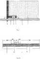
- Step S3)forming a gate insulating layer 8 on the substrate 1 after the step S2), and forming a contact hole (not shown) by a patterning process, as shown in Fig. 4 .
- the gate insulating layer 8is deposited on the substrate 1 after the step S2), and the contact hole is formed by a photolithographic process.
- the deposition of the gate insulating layer 8may be continuously performed by a PECVD method, and the thickness of the gate insulating layer 8 may be 1000 - 4000 ⁇ .
- the gate insulating layer 8may be formed of silicon oxide SiO x , silicon nitride SiN x , silicon oxynitride SiN x O y , or may be formed of an insulating metal oxide such as Al 2 O 3 .
- the reacting gases used to form the silicon nitridemay be SiH 4 , NH 3 and N 2 , or may be SiH 2 Cl 2 , NH 3 and N 2
- the reacting gases used to form the silicon oxidemay be SiH 4 and N 2 O
- the reacting gases used to form the silicon oxynitridemay be SiH 4 , N 2 O, NH 3 and N 2 .
- Step S4)forming the gate electrode and the gate scanning line on the substrate 1 after the step S3) by a patterning process.
- a gate metal filmis deposited on the substrate 1 after the step S3), and the gate electrode 9 and the gate scanning line 11 are formed by a photolithographic process.
- the gate metal filmmay be deposited by a sputtering method or a thermal evaporation method, and the thickness of the gate metal film may be 4000 - 15000 ⁇ .
- the gate metal filmmay be made of a single layer formed by any one of Cr, W, Cu, Ti, Ta, and Mo, or may be made of alloys of any one of the above-mentioned metals, or may be made of a multi-layer formed by any combination of the above-mentioned metals.
- the gate electrode 9 and the gate scanning line 11are formed by a photolithographic process, as shown in Fig. 5 .
- etching barrier layer 4may use a lamination structure.
- the etching barrier layer 4uses a dual-layer structure.
- the layer contacting the metal oxide semiconductor layer 3is made of SiO 2 and is formed by a low speed deposition manner
- the layer away from the metal oxide semiconductor layer 3is made of SiN x and is formed by a high speed deposition manner.
- the TFTis a top gate type TFT.
- the embodiments of the present inventionare applicable to manufacture an array substrate having a metal oxide TFT of bottom gate type as well.
- the gate insulating layer 8may also have a lamination structure in addition to the etching barrier layer 4.
- the gate insulating layer 8may have a dual-layer structure. In the dual-layer structure of the gate insulating layer 8, the layer contacting the metal oxide semiconductor layer 3 is made of SiO 2 and is formed by a low speed deposition manner, whereas the layer away from the metal oxide semiconductor layer 3 is made of SiN x and is formed by a high speed deposition manner.
- the portions of the etching barrier layer and the gate insulating layer that contact the metal oxide semiconductor layerare formed by a low speed deposition manner, these portions are more compact, and thus a good interface can be formed between these portions and the metal oxide semiconductor layer 3, which is advantageous in increasing the stability of the TFT.
- the portions of the etching barrier layer and the gate insulating layer that are away from the metal oxide semiconductor layer 3are formed by a high speed deposition manner, the depositing speed is relatively fast, and thus the production efficiency can be effectively increased.
- the embodiments of the present inventionprovide the manufacturing method of the array substrate with metal oxide TFT by four patterning processes. Compared with the conventional method using six patterning processes, the number of the patterning processes is reduced by two, thus the manufacturing method can be simplified, the production efficiency can be increased and the production cost can be reduced.
- the embodiments of the present inventionare especially suitable for the TFT-LCD with large size and high resolution and the AMOLED.
Landscapes
- Thin Film Transistor (AREA)
- Devices For Indicating Variable Information By Combining Individual Elements (AREA)
Description
- Embodiments of the present invention relate to a manufacturing method of a TFT array substrate.
- At present, flat panel displays have been gradually replacing the bulky CRT displays. The common flat panel displays include liquid crystal displays (LCDs) and organic light emitting diode displays.
- In the LCD, each pixel is driven by a corresponding thin film transistor (TFT) on a TFT array substrate and displays image in cooperation with peripheral driving circuits. In the active matrix organic light emission display (AMOLED), each pixel is driven by a corresponding thin film transistor (TFT) on a TFT array substrate and displays image in cooperation with peripheral driving circuits. In the above mentioned displays, the TFT functions as a switching element, and is a key element for achieving image display in the above mentioned displays. The characteristics of the TFT directly determine the development of high performance flat panel displays.
- The TFTs that have been industrialized include amorphous silicon TFTs, polysilicon TFTs, monocrystalline silicon TFTs and the like. Among these TFTs, the amorphous silicon TFTs is most widely used to manufacture the array substrate of the flat panel display.
- Recently, metal oxide TFTs draw more and more attentions. The metal oxide TFTs have the advantage of high carrier mobility so that they can be made very small, and in this case, the resolution of the flat panel display can be increased and the display effect can be improved. Furthermore, the metal oxide TFTs also have such advantages as less occurrence of characteristic unevenness, low cost of materials and processes, low temperature of processes, suitable to a coating process, high transparency, large band gap and the like.
- The array substrate comprising the metal oxide TFT is generally manufactured by using six photolithographic processes. If the number of the photolithographic processes can be reduced, that is, if the number of the masks used in the manufacturing process can be reduced, it is possible to increase the production efficiency and reduce the production cost.
CN 101 770 124 A discloses a TFT-LCD array substrate and a manufacturing method thereof, wherein the manufacturing method comprises: (1) depositing a gate metal-layer thin film on a substrate, forming a figure comprising a gate electrode and a gate line; (2) depositing a gate insulating layer thin film, a semiconductor layer thin film and a barrier layer thin film on the on the substrate subjected to the step (1), forming a figure comprising figures of a gate insulating layer, a semiconductor layer and a barrier layer, wherein the barrier layer is used for preventing the semiconductor layer of a TFT channel from being etched; and (3) depositing an ohmic contact layer thin film, a transparent conductive layer thin film, a source-drain metal layer thin film and a passivation layer thin film on the substrate subjected to the step (2), and forming a figure comprising figures of an ohmic contact layer, a pixel electrode, a data line, a source electrode, a drain electrode and a passivation layer.CN 102 184 865 A discloses a TFT and a manufacturing method thereof comprising: forming a source electrode and a drain electrode which are mutually insulated on a substrate; forming a patterned oxide semiconductor layer and a pixel semiconductor layer on the substrate at the same time; forming a patterned etched barrier layer on the oxide semiconductor layer, and exposing a part of patterned oxide semiconductor layer positioned on the two sides of the patterned etched barrier layer; forming a gate insulating layer on the substrate; forming the part of patterned oxide semiconductor layer exposed by the patterned etched barrier layer into two ohmic contact layers and forming the pixel semiconductor layer into a pixel electrode at the same time in the process of forming the gate insulating layer; and forming a gate electrode on the gate insulating layer above the patterned oxide semiconductor layer.US 2011/163310 A1 disclose TFT including a channel layer, an etch stop multi-layer, a source, a drain, a gate, and a gate insulation layer. The etch stop multi-layer may include a first etch stop layer and a second etch stop layer. The second etch stop layer may prevent or reduce an etchant from contacting the channel layer.- It is an object of the present invention to provide a manufacturing method of a TFT array substrate in which the number of required photolithographic processes, in particular the number of the masks used in the manufacturing process, is reduced, in order to increase the production efficiency and to reduce the production cost.
- The object is solved by the features of the independent claim. Further embodiments are defined in the dependent claims.
- In the manufacturing method according to the embodiments of embodiment, four patterning processes are used to manufacture the TFT array substrate. Compared with the conventional method using six patterning processes, the number of the patterning processes are reduced by two, thus the manufacturing process can be simplified, the production efficiency can be increased, and the production cost can be reduced.
- In order to clearly illustrate the technical solution of the embodiments of the invention, the drawings of the embodiments will be briefly described in the following; it is obvious that the described drawings are only related to some embodiments of the invention and thus are not limitative of the invention which is defined in the claims.
Fig. 1 is a schematic plan view showing a TFT array substrate manufactured by a manufacturing method of a TFT array substrate according to an embodiment of the present invention;Figs. 2a-2e are schematic cross-sectional views showing the TFT array substrate during a first patterning process in the manufacturing method of the TFT array substrate according to the embodiment of the present invention;Fig. 2f is a schematic cross-sectional view showing the TFT array substrate after the first patterning process in the manufacturing method of the TFT array substrate according to the embodiment of the present invention;Figs. 3a-3e are schematic cross-sectional views showing the TFT array substrate during a second patterning process in the manufacturing method of the TFT array substrate according to the embodiment of the present invention;Fig. 3f is a schematic cross-sectional view showing the TFT array substrate after the second patterning process in the manufacturing method of the TFT array substrate according to the embodiment of the present invention;Fig. 4 is a schematic cross-sectional view showing the TFT array substrate after a third patterning process in the manufacturing method of the TFT array substrate according to the embodiment of the present invention; andFig. 5 is a schematic cross-sectional view showing the TFT array substrate after a fourth patterning process in the manufacturing method of the TFT array substrate according to the embodiment of the present invention.- In order to make objects, technical solutions and advantages of the embodiments of the invention apparent, the technical solutions of the embodiment will be described in a clearly and fully understandable way in connection with the drawings related to the embodiments of the invention. It is obvious that the described embodiments are just a part but not all of the embodiments of the invention. Based on the described embodiments herein, those skilled in the art can obtain other embodiment(s), without any inventive work, which should be within the scope of the invention which is defined by the claims.
- In the following description, patterning processes includes a photolithographic process and other processes used to form predetermined patterns, such as a printing process, an ink jetting process and the like. The photolithographic process includes such steps as exposing, developing, etching and the like.
- The following description is made based on a single pixel unit, but other pixel units may be formed in the same manner.
- Embodiments of the present invention provide a manufacturing method of a TFT array substrate. The manufacturing method of the TFT array substrate includes the following steps: respectively forming a metal oxide semiconductor layer, an etching barrier layer, a source electrode, a data line, a drain electrode, a pixel electrode, a gate insulating layer, a contact hole, a gate electrode and a gate scanning line on a substrate by patterning processes, wherein the metal oxide semiconductor layer and the etching barrier layer are formed by a same patterning process, and the source electrode, the drain electrode, the transparent pixel electrode and the data line are formed by another same patterning process.
- The above manufacturing method may include the following steps:
- Step S1): forming the metal oxide semiconductor layer and the etching barrier layer on the substrate by the same patterning process with a gray-tone or half-tone mask;
- Step S2): forming the source electrode, the drain electrode, the data line and the pixel electrode on the substrate after the step S1) by the another same patterning process with a gray-tone or half-tone mask;
- Step S3): forming the gate insulating layer on the substrate after the step S2), and forming the contact hole by a patterning process;
- Step S4): forming the gate electrode and the gate scanning line on the substrate after the step S3) by a patterning process.
- Shown in
Fig. 1 is a plan view of a TFT array substrate manufactured by the manufacturing method according to this embodiment. - The TFT array substrate includes a plurality of
gate scanning lines 11 and a plurality ofdata lines 10, thegate scanning lines 11 and thedata lines 10 intersect with each other to define a plurality of pixel units arranged in a matrix. Each pixel unit includes a TFT that functions as a switching element and apixel electrode 5 that uses to control the alignment of liquid crystal molecules. - The TFT of each pixel unit includes: a metal oxide semiconductor layer, functioning as an active layer; an etching barrier layer, formed on the metal oxide semiconductor layer; a source electrode, one end thereof provided on the metal oxide semiconductor layer; a drain electrode, one end thereof opposing to the source electrode and provided on the metal oxide semiconductor layer; a gate insulating layer, formed to cover the source electrode, the drain electrode and the etching barrier layer; and a gate electrode, formed on the gate insulating layer and located above the metal oxide semiconductor layer, In the TFT, the gate electrode is electrically connected with the corresponding gate scanning line, the source electrode is electrically connected with the corresponding data line, and the drain electrode is electrically connected with the pixel electrode.
Figs. 2-5 are sectional views taken along the line A-B inFig. 1 . Hereinafter, the manufacturing method of the TFT array substrate according to this embodiment will be described in detail in connection withFigs. 2-5 .- In this embodiment, the manufacturing method of the TFT array substrate includes the following steps.
- Step S1): forming the metal
oxide semiconductor layer 3 and theetching barrier layer 4 on a substrate by a patterning process with a gray-tone or half-tone mask, as shown inFig. 2f . - First, a
modification layer 2 is deposited on thesubstrate 1, and then a metal oxide semiconductor film 3' and an etching barrier film 4' are deposited in this order on themodification layer 2. Theetching barrier layer 4 and the metaloxide semiconductor layer 3 are formed by the patterning process using the gray-tone or half-tone mask. - For example, the step S1) may include the following steps.
- S11) depositing the
modification layer 2, the metal oxide semiconductor film 3' and the etching barrier film 4' in this order on thesubstrate 1. - S12) coating a layer of
photoresist 12 on thesubstrate 1 after the step S11). - S13) performing exposing and developing processes on the photoresist by using the gray-tone or half-tone mask. A non-transmissive region, a partially-transmissive region and a transmissive region are provided in the half-tone or gray-tone mask. If the
photoresist 12 is a positive photoresist, the non-transmissive region, the partially-transmissive region and the transmissive region in the gray-tone or half-tone mask respectively correspond to a photoresist completely retained region NP, a photoresist partially retained region HP and a photoresist completely removed region WP after the exposing and the developing processes of the photoresist. If thephotoresist 12 is a negative photoresist, the non-transmissive region, the partially-transmissive region and the transmissive region in the gray-tone or half-tone mask respectively correspond to a photoresist completely removed region WP, a photoresist partially retained region HP and a photoresist completely retained region NP after the exposing and the developing processes of the photoresist. The photoresist of the photoresist completely retained region NP is completely retained, and the photoresist completely retained region NP corresponds to the region for forming the etching barrier layer. The thickness of the photoresist of the photoresist partially retained region HP is thinner than the thickness of the photoresist of the photoresist completely retained region NP, and the photoresist partially retained region corresponds to the region for forming the metal oxide semiconductor layer. The photoresist of the photoresist completely removed region WP is completely removed, and the regions which are not covered by the photoresist are all photoresist completely removed region WP, as shown inFig. 2a . - The principle of forming the photoresist partially retained region HP is as follows. This region is exposed by using the partially-transmissive region with slits in the gray-tone or half-tone mask, Whether the
photoresist 12 is a positive photoresist or a negative photoresist, the diffraction effect and the interference effect of the slits allow the intensity of the light reaching this region upon performing the exposing process to be weaker than the intensity of the light of the transmissive region. Therefore, the photoresist of the partially-transmissive region is less exposed than the photoresist of the transmissive region, so that the thickness of the photoresist of the photoresist partially retained region HP is thinner than the thickness of the photoresist of the photoresist completely retained region NP. - S14) performing an etching process after the step S13), so as to form the metal
oxide semiconductor layer 3. - As shown in
Fig. 2b , a first etching process is performed by using a dry etching method, so as to etch away the etching barrier film of the photoresist completely removed region WP. As shown inFig. 2c , a second etching process is performed by using a wet etching method, so as to etch away the metal oxide semiconductor film of the photoresist completely removed region WP. Thereby, the metaloxide semiconductor layer 3 is formed. - S15) performing an ashing treatment after the step S14), so as to remove the photoresist of the photoresist partially retained region, as shown in
Fig. 2d . - S16) performing an etching process after the step S15), so as to form the etching barrier layer.
- As shown in
Fig. 2e , a third etching process is performed by using a dry etching method, so as to etch away the etching barrier film of the photoresist partially retained region HP. Thereby, theetching barrier layer 4 is formed. - S17) peeling off the remaining photoresist to expose the metal
oxide semiconductor layer 3 and theetching barrier layer 4, as shown inFig. 2f . - In the above-mentioned steps, the deposition of the
modification layer 2 on thesubstrate 1 may be performed continuously by using a Plasma Enhanced Chemical Vapor Deposition (PECVD) method, and the thickness of themodification layer 2 may be in a range of 500 to 2000 Å. Themodification layer 2 may be formed of silicon oxide SiOx, silicon nitride SiNx, silicon oxynitride SiNxOy, or may be formed of an insulating metal oxide such as Al2O3. When using the PECVD method, the reacting gases used to form the silicon nitride may be SiH4, NH3 and N2 or may be SiH2Cl2, NH3 and N2, the reacting gases used to form the silicon oxide may be SiH4 and N2O, and the reacting gases used to form the silicon oxynitride may be SiH4, N2O, NH3 and N2. Themodification layer 2 allows the posterior metal oxide semiconductor layer to well form on thesubstrate 1, and thus the metaloxide semiconductor layer 3 can be protected and the stability of the metaloxide semiconductor layer 3 can be improved. - The deposition of the metal oxide semiconductor film 3' on the
substrate 1 may be performed by using a sputtering method or a thermal evaporation method. The thickness of the metal oxide semiconductor film may be 100 - 4000 Å. The metal oxide semiconductor film may be made of an amorphous IGZO, or may be made of HIZO, IZO, a-InZnO, a-InZnO, ZnO:F, In2O3:Sn, In2O3:Mo, Cd2SnO4, ZnO:Al, TiO2:Nb, Cd-Sn-O or other metal oxides. - The deposition of the etching barrier film 4' may be performed by using a PECVD method, and the thickness of the etching barrier film may be 500 - 4000 Å. The etching barrier film may be formed of silicon oxide SiOx, silicon nitride SiNx, silicon oxynitride SiNxOy, or may be formed of an insulating metal oxide such as Al2O3. When using the PECVD method, the reacting gases used to form the silicon nitride may be SiH4, NH3 and N2 or may be SiH2Cl2, NH3 and N2, the reacting gases used to form the silicon oxide may be SiH4 and N2O, and the reacting gases used to form the silicon oxynitride may be SiH4, N2O, NH3 and N2.
- Step S2): forming the
drain electrode 6, thesource electrode 7, the data line (not shown inFig. 3 ) and thetransparent pixel electrode 5 on thesubstrate 1 after the step S1) by a patterning process with a gray-tone or half-tone mask, as shown inFig. 3f . - The step S2) may include the following steps.
- S21) depositing a transparent conductive film 5' and a source/drain metal film 6' in this order on the
substrate 1. - S22) coating a layer of
photoresist 12 on thesubstrate 1 after the step S21). - S23) performing exposing and developing processes on the
photoresist 12 by using the gray-tone or half-tone mask. A non-transmissive region, a partially-transmissive region and a transmissive region are provided in the half-tone or gray-tone mask. If thephotoresist 12 is a positive photoresist, the non-transmissive region, the partially-transmissive region and the transmissive region in the gray-tone or half-tone mask respectively correspond to a photoresist completely retained region NP, a photoresist partially retained region HP and a photoresist completely removed region WP after the exposing and the developing processes of the photoresist. If thephotoresist 12 is a negative photoresist, the non-transmissive region, the partially-transmissive region and the transmissive region in the gray-tone or half-tone mask respectively correspond to a photoresist completely removed region WP, a photoresist partially retained region HP and a photoresist completely retained region NP after the exposing and the developing processes of the photoresist. The photoresist completely retained region NP corresponds to the region to form the data lines, the source electrode and the drain electrode, the photoresist partially retained region HP corresponds to the region to form the transparent pixel electrode, and the regions which are not covered by the photoresist are all photoresist completely removed regions WP, as shown inFig. 3a . - S24) performing an etching process after the step S23), so as to form the
source electrode 7 and the data lines. - As shown in
Fig. 3b , a first etching process is performed to etch away the source/drain metal film 6' of the photoresist completely removed region WP. As shown inFig. 3c , a second etching process is performed to etch away the transparent conductive film 5' of the photoresist completely removed region WP. Thereby, thesource electrode 7 and the data lines (not shown in the figure) are formed. - S25) performing an ashing treatment after the step S24), so as to remove the photoresist of the photoresist partially retained region HP, as shown in
Fig. 3d . - S26) performing an etching process after the step S25), so as to form the
drain electrode 6 and thetransparent pixel electrode 5. - As shown in
Fig. 3e , a third etching process is performed to etch away the source/drain metal film 6' of the photoresist partially retained region HP. Thereby, thedrain electrode 6 and thetransparent pixel electrode 5 are formed. - S27) peeling off the remaining photoresist to expose the
drain electrode 6, thesource electrode 7, thetransparent pixel electrode 5 and the data lines. - Since the
modification layer 2 is deposited on the substrate in the step S1), a TFT channel formed between thedrain electrode 6 and thesource electrode 7 can be effectively protected by themodification layer 2 upon performing the deposition of the transparent conductive film in the above mentioned steps, and thus the direct contact between the TFT channel and thesubstrate 1 which otherwise will form a bad interface can be avoided. Meanwhile, by employing themodification layer 2, the metal oxide semiconductor layer formed in the first patterning process of the step S1) can be more stable to avoid defects. - In this embodiment, since the metal oxide semiconductor layer is formed of the metal oxide semiconductor with wide band gap such as IGZO, photocurrent will not occur when the metal oxide semiconductor layer is irradiated by the visible light. Therefore, a light shielding layer is not used in this embodiment, and the modification layer is formed on the substrate directly.
- In the above mentioned steps, the transparent conductive film may be deposited by a sputtering method or a thermal evaporation method after the step S1), and the thickness of the transparent conductive film may be 300 - 1500 Å. The thickness of the source/drain metal film may be 2000 - 3000 Å. The transparent conductive film may be made of ITO, or may be made of other metals and metal oxides. The source/drain metal film may be made of a sing layer formed by any one of Cr, W, Ti, Ta, Mo, Al and Cu, or may be made of alloys of any one of the above-mentioned metals, or may be made of a multi-layer formed of any combination of the above-mentioned metals.
- Step S3): forming a
gate insulating layer 8 on thesubstrate 1 after the step S2), and forming a contact hole (not shown) by a patterning process, as shown inFig. 4 . - In this step, the
gate insulating layer 8 is deposited on thesubstrate 1 after the step S2), and the contact hole is formed by a photolithographic process. - In this step, the deposition of the
gate insulating layer 8 may be continuously performed by a PECVD method, and the thickness of thegate insulating layer 8 may be 1000 - 4000 Å. Thegate insulating layer 8 may be formed of silicon oxide SiOx, silicon nitride SiNx, silicon oxynitride SiNxOy, or may be formed of an insulating metal oxide such as Al2O3. When using the PECVD method, the reacting gases used to form the silicon nitride may be SiH4, NH3 and N2, or may be SiH2Cl2, NH3 and N2, the reacting gases used to form the silicon oxide may be SiH4 and N2O, and the reacting gases used to form the silicon oxynitride may be SiH4, N2O, NH3 and N2. - Step S4): forming the gate electrode and the gate scanning line on the
substrate 1 after the step S3) by a patterning process. - In this step, a gate metal film is deposited on the
substrate 1 after the step S3), and thegate electrode 9 and thegate scanning line 11 are formed by a photolithographic process. - In this step, the gate metal film may be deposited by a sputtering method or a thermal evaporation method, and the thickness of the gate metal film may be 4000 - 15000 Å. The gate metal film may be made of a single layer formed by any one of Cr, W, Cu, Ti, Ta, and Mo, or may be made of alloys of any one of the above-mentioned metals, or may be made of a multi-layer formed by any combination of the above-mentioned metals. Next, the
gate electrode 9 and thegate scanning line 11 are formed by a photolithographic process, as shown inFig. 5 . - The difference of this embodiment from the
above embodiment 1 is in that theetching barrier layer 4 may use a lamination structure. - In this embodiment, the
etching barrier layer 4 uses a dual-layer structure. In the dual-layer structure of theetching barrier layer 4, the layer contacting the metaloxide semiconductor layer 3 is made of SiO2 and is formed by a low speed deposition manner, and the layer away from the metaloxide semiconductor layer 3 is made of SiNx and is formed by a high speed deposition manner. - In the above descriptions, the TFT is a top gate type TFT. However, the embodiments of the present invention are applicable to manufacture an array substrate having a metal oxide TFT of bottom gate type as well. When the TFT is of bottom gate type, the
gate insulating layer 8 may also have a lamination structure in addition to theetching barrier layer 4. For example, thegate insulating layer 8 may have a dual-layer structure. In the dual-layer structure of thegate insulating layer 8, the layer contacting the metaloxide semiconductor layer 3 is made of SiO2 and is formed by a low speed deposition manner, whereas the layer away from the metaloxide semiconductor layer 3 is made of SiNx and is formed by a high speed deposition manner. - According to this embodiment, since the portions of the etching barrier layer and the gate insulating layer that contact the metal oxide semiconductor layer are formed by a low speed deposition manner, these portions are more compact, and thus a good interface can be formed between these portions and the metal
oxide semiconductor layer 3, which is advantageous in increasing the stability of the TFT. On the other hand, since the portions of the etching barrier layer and the gate insulating layer that are away from the metaloxide semiconductor layer 3 are formed by a high speed deposition manner, the depositing speed is relatively fast, and thus the production efficiency can be effectively increased. - The embodiments of the present invention provide the manufacturing method of the array substrate with metal oxide TFT by four patterning processes. Compared with the conventional method using six patterning processes, the number of the patterning processes is reduced by two, thus the manufacturing method can be simplified, the production efficiency can be increased and the production cost can be reduced. The embodiments of the present invention are especially suitable for the TFT-LCD with large size and high resolution and the AMOLED.
- The embodiments described above are only exemplary implementation of the present invention, and are not used to limit the protection scope of the present invention, which is defined by the appended claims.
Claims (7)
- A manufacturing method of a TFT array substrate, including the following steps: respectively forming a metal oxide semiconductor layer (3), an etching barrier layer (4), a source electrode (7), a data line (10), a drain electrode (6), a pixel electrode (5), a gate insulating layer (8), a contact hole, a gate electrode (9) and a gate scanning line (11) on a substrate (1) by patterning processes, wherein the metal oxide semiconductor layer (3) and the etching barrier layer (4) are formed by a first patterning process, and the source electrode (7), the drain electrode (6), the pixel electrode (5) and the data line (10) are formed by a second patterning process,
wherein the manufacturing method includes the following steps:Step S1): forming the metal oxide semiconductor layer (3) and the etching barrier layer (4) on the substrate by the first patterning process with a first gray-tone or half-tone mask;Step S2): forming the source electrode (7), the drain electrode (6), the data line (10) and the pixel electrode (5) on the substrate (1) after the step S1) by the second patterning process with a second gray-tone or half-tone mask;Step S3): forming the gate insulating layer (8) on the substrate (1) after the step S2), and forming the contact hole by a third patterning process; andStep S4): forming the gate electrode (9) and the gate scanning line (11) on the substrate (1) after the step S3) by a forth patterning process,wherein the step S1) includes the following steps:S11) depositing a metal oxide semiconductor film (3') and an etching barrier film (4') in this order on the substrate (1);S12) coating a layer of photoresist on the substrate (1) after the step S11);S13) using the first gray-tone or half-tone mask to perform exposing and developing processes on the photoresist so as to form a photoresist completely retained region, a photoresist partially retained region and photoresist completely removed regions, the photoresist completely retained region corresponding to a region for forming the etching barrier layer, the photoresist partially retained region corresponding to a region for forming the metal oxide semiconductor layer, and regions not covered by the photoresist corresponding to the photoresist completely removed region;S14) performing an etching process after the step S13) so as to form the metal oxide semiconductor layer (3);S15) performing an ashing treatment after the step S14) so as to remove the photoresist of the photoresist partially retained region;S16) performing an etching process after the step S15) so as to form the etching barrier layer (4); andS17) peeling off a remaining portion of the photoresist,wherein in the step S11), a modification layer (2) is firstly deposited on the substrate, then, the metal oxide semiconductor film (3'), and the etching barrier film (4') are deposited sequentially on the modification layer (2),wherein the etching barrier layer (4) is deposited as a dual-layer structure made of a SiO2 layer contacting the metal oxide semiconductor layer and being formed by a low speed deposition manner, and of a SiNx layer away from the metal oxide semiconductor layer and being formed by a high speed deposition manner;
the deposition of the modification layer (2) is performed by a PECVD method; and
the modification layer (2) is made of an oxide, a nitride or an oxynitride compound, and a thickness of the modification layer is in a range of 500 - 2000 Å. - The manufacturing method according to claim 1, wherein in the step S11), the deposition of the metal oxide semiconductor film (3') is performed by a sputtering method or a thermal evaporation method, the metal oxide semiconductor film (3') is made of amorphous IGZO, HIZO, IZO, a-InZnO, a-InZnO, ZnO:F, In2O3:Sn, In2O3:Mo, Cd2SnO4, ZnO:Al, TiO2:Nb or Cd-Sn-O, a thickness of the metal oxide semiconductor film is 100 - 2000 Å; and
the deposition of the etching barrier film (4') on the metal oxide semiconductor film (3') is performed by a PECVD method, the etching barrier film (4') is made of silicon oxide, silicon nitride or silicon oxynitride, and a thickness of the etching barrier film (4') is 500 - 4000 Å. - The manufacturing method according to claim 1, wherein the step S2) includes the following steps:S21) depositing a transparent conductive film (5') and a source/drain metal film (6') in this order on the substrate;S22) coating a layer of photoresist on the substrate after the step S21);S23) using the second gray-tone or half-tone mask to perform exposing and developing processes on the photoresist so as to form a photoresist completely retained region, a photoresist partially retained region and photoresist completely removed regions, the photoresist completely retained region corresponding to regions for forming the data line (10), the source electrode (7) and the drain electrode (6), the photoresist partially retained region corresponding to a region for forming the pixel electrode (5), and regions not covered by the photoresist corresponding to the photoresist completely removed regions;S24) performing an etching process after the step S23) so as to form the source electrode (6) and the data line (10);S25) performing an ashing treatment after the step S24) so as to remove the photoresist of the photoresist partially retained region;S26) performing an etching process after the step S25) so as to form the drain electrode (6) and the pixel electrode (5); andS27) peeling off a remaining portion of the photoresist.
- The manufacturing method according to claim 3, wherein in the step S21), the deposition of the transparent conductive film (5') is performed by a sputtering method or a thermal evaporation method, the transparent conductive film (5') is made of ITO or other transparent metal oxides, a thickness of the transparent conductive film (5') is 300 - 1500 Å; and
the deposition of the source/drain metal film (6') is performed by a sputtering method or a thermal evaporation method, the source/drain metal film (6') is made of Cr, W, Ti, Ta, Mo, Al, Cu or an alloy of any one of these metals, and a thickness of the source/drain metal film (6') is 2000 - 3000 Å. - The manufacturing method according to claim 1, wherein in the step S3), the gate insulating layer (8) is formed by a PECVD method after the step S2), the gate insulating layer (8) is made of an oxide, a nitride or an oxynitride compound, and a thickness of the gate insulating layer is 1000 - 4000 Å.
- The manufacturing method according to claim 1, wherein in the step S4), a gate metal film is deposited on the gate insulating layer (8), and the gate electrode (9) and the gate scanning line (11) are formed by a photolithographic process;
the deposition of the gate metal film on the gate insulating layer (8) is performed by a sputtering method or a thermal evaporation method, the gate metal film is made of Cr, W, Cu, Ti, Ta, Mo or an alloy of any one of these metals, and a thickness of the gate metal film is 4000 - 15000 Å. - The manufacturing method according to claim 1, wherein the TFT includes: the metal oxide semiconductor layer (3), functioning as an active layer; the etching barrier layer (4), formed on the metal oxide semiconductor layer (3); the source electrode (7), one end thereof provided on the metal oxide semiconductor layer (3); the drain electrode (6), one end thereof opposing to the source electrode (7) and provided on the metal oxide semiconductor layer (3); the gate insulating layer (8), formed to cover the source electrode (7), the drain electrode (6) and the etching barrier layer (4); and the gate electrode (9), formed on the gate insulating layer (8) and located above the metal oxide semiconductor layer (3).
Applications Claiming Priority (2)
| Application Number | Priority Date | Filing Date | Title |
|---|---|---|---|
| CN201210010351.1ACN102651341B (en) | 2012-01-13 | 2012-01-13 | Manufacturing method of TFT (Thin Film Transistor) array substrate |
| PCT/CN2012/086312WO2013104228A1 (en) | 2012-01-13 | 2012-12-10 | Method for manufacturing tft array substrate |
Publications (3)
| Publication Number | Publication Date |
|---|---|
| EP2804207A1 EP2804207A1 (en) | 2014-11-19 |
| EP2804207A4 EP2804207A4 (en) | 2015-10-14 |
| EP2804207B1true EP2804207B1 (en) | 2018-10-31 |
Family
ID=46693313
Family Applications (1)
| Application Number | Title | Priority Date | Filing Date |
|---|---|---|---|
| EP12861052.4AActiveEP2804207B1 (en) | 2012-01-13 | 2012-12-10 | Method for manufacturing tft array substrate |
Country Status (6)
| Country | Link |
|---|---|
| US (1) | US9202892B2 (en) |
| EP (1) | EP2804207B1 (en) |
| JP (1) | JP6129206B2 (en) |
| KR (1) | KR101620674B1 (en) |
| CN (1) | CN102651341B (en) |
| WO (1) | WO2013104228A1 (en) |
Families Citing this family (28)
| Publication number | Priority date | Publication date | Assignee | Title |
|---|---|---|---|---|
| CN102651341B (en)* | 2012-01-13 | 2014-06-11 | 京东方科技集团股份有限公司 | Manufacturing method of TFT (Thin Film Transistor) array substrate |
| CN102629590B (en) | 2012-02-23 | 2014-10-22 | 京东方科技集团股份有限公司 | Thin film transistor array substrate and manufacturing method thereof |
| KR102010789B1 (en)* | 2012-12-27 | 2019-10-21 | 엘지디스플레이 주식회사 | Transparent organic light emitting display device and method for manufacturing the same |
| CN103178021B (en)* | 2013-02-28 | 2015-02-11 | 京东方科技集团股份有限公司 | Oxide thin-film transistor array substrate, manufacturing method for same and display panel |
| CN103258827B (en)* | 2013-04-28 | 2016-03-23 | 京东方科技集团股份有限公司 | Array base palte and preparation method thereof, display unit |
| CN103354218B (en)* | 2013-06-28 | 2016-12-28 | 京东方科技集团股份有限公司 | Array base palte and preparation method thereof and display device |
| CN103715137B (en)* | 2013-12-26 | 2018-02-06 | 京东方科技集团股份有限公司 | Array base palte and its manufacture method, display device |
| CN103744240A (en)* | 2013-12-27 | 2014-04-23 | 深圳市华星光电技术有限公司 | Array substrate and liquid crystal display panel using the same |
| CN103745954B (en) | 2014-01-03 | 2017-01-25 | 京东方科技集团股份有限公司 | Display device, array substrate and manufacturing method of array substrate |
| CN104091784A (en)* | 2014-07-11 | 2014-10-08 | 合肥鑫晟光电科技有限公司 | Array substrate manufacturing method |
| CN104167365A (en)* | 2014-08-06 | 2014-11-26 | 京东方科技集团股份有限公司 | Metal oxide thin-film transistor, array substrate, manufacturing method of metal oxide thin-film transistor and display device |
| CN104810321A (en)* | 2015-04-30 | 2015-07-29 | 京东方科技集团股份有限公司 | Production method of TFT (thin film transistor) array substrate and display device |
| TWI542715B (en)* | 2015-09-21 | 2016-07-21 | 友達光電股份有限公司 | Method for producing crystalline indium gallium zinc semiconductor layer and thin film transistor |
| CN105206570B (en)* | 2015-10-27 | 2018-11-23 | 深圳市华星光电技术有限公司 | A kind of display panel and its manufacturing method |
| CN105655359A (en)* | 2016-03-31 | 2016-06-08 | 武汉华星光电技术有限公司 | Method for manufacturing TFT (thin-film transistor) substrates |
| CN105702586B (en)* | 2016-04-28 | 2019-06-07 | 京东方科技集团股份有限公司 | A kind of thin film transistor (TFT), array substrate, its production method and display device |
| CN105914229B (en)* | 2016-06-24 | 2017-12-15 | 京东方科技集团股份有限公司 | A kind of AMOLED display base plates and preparation method thereof, display device |
| CN106298546A (en)* | 2016-10-31 | 2017-01-04 | 京东方科技集团股份有限公司 | A kind of thin film transistor (TFT), its manufacture method, array base palte and display floater |
| CN106876332B (en)* | 2017-03-21 | 2020-04-21 | 京东方科技集团股份有限公司 | Display device, fingerprint identification unit, thin film transistor and method of manufacturing the same |
| CN107093583A (en)* | 2017-05-03 | 2017-08-25 | 京东方科技集团股份有限公司 | A kind of array base palte and preparation method thereof, display device |
| CN107464836B (en)* | 2017-07-19 | 2020-04-10 | 深圳市华星光电半导体显示技术有限公司 | Manufacturing method of top gate type thin film transistor and top gate type thin film transistor |
| CN107689345B (en)* | 2017-10-09 | 2020-04-28 | 深圳市华星光电半导体显示技术有限公司 | TFT substrate and manufacturing method thereof, and OLED panel and manufacturing method thereof |
| CN108346704B (en)* | 2018-02-01 | 2021-04-09 | 惠科股份有限公司 | Thin film transistor and method of manufacturing the same |
| CN110620080A (en)* | 2019-10-23 | 2019-12-27 | 成都中电熊猫显示科技有限公司 | Manufacturing method of array substrate, array substrate and display panel |
| CN110610949A (en)* | 2019-10-23 | 2019-12-24 | 成都中电熊猫显示科技有限公司 | Manufacturing method of array substrate and array substrate |
| CN111403337A (en)* | 2020-03-31 | 2020-07-10 | 成都中电熊猫显示科技有限公司 | Array substrate, display panel and manufacturing method of array substrate |
| CN114402430A (en)* | 2021-12-17 | 2022-04-26 | 昆山龙腾光电股份有限公司 | Array substrate, manufacturing method and display panel |
| CN116799016B (en)* | 2023-07-28 | 2024-08-09 | 惠科股份有限公司 | Array substrate, manufacturing method thereof and display panel |
Citations (1)
| Publication number | Priority date | Publication date | Assignee | Title |
|---|---|---|---|---|
| US20110284847A1 (en)* | 2010-05-21 | 2011-11-24 | Semiconductor Energy Laboratory Co., Ltd. | Semiconductor device |
Family Cites Families (18)
| Publication number | Priority date | Publication date | Assignee | Title |
|---|---|---|---|---|
| CN100530549C (en)* | 2004-08-23 | 2009-08-19 | 株式会社半导体能源研究所 | Laser irradiation apparatus, irradiation method, and method of manufacturing semiconductor device |
| JP2006324368A (en) | 2005-05-18 | 2006-11-30 | Dainippon Printing Co Ltd | Thin film transistor mounted panel and method for manufacturing the same |
| KR101410926B1 (en)* | 2007-02-16 | 2014-06-24 | 삼성전자주식회사 | Thin film transistor and manufacturing method thereof |
| JP5354999B2 (en)* | 2007-09-26 | 2013-11-27 | キヤノン株式会社 | Method for manufacturing field effect transistor |
| JP5213422B2 (en)* | 2007-12-04 | 2013-06-19 | キヤノン株式会社 | Oxide semiconductor element having insulating layer and display device using the same |
| CN101630098B (en)* | 2008-07-18 | 2010-12-08 | 北京京东方光电科技有限公司 | TFT-LCD array substrate and manufacturing method thereof |
| TWI585955B (en)* | 2008-11-28 | 2017-06-01 | 半導體能源研究所股份有限公司 | Light sensor and display device |
| US8610119B2 (en)* | 2008-12-24 | 2013-12-17 | 3M Innovative Properties Company | Stability enhancements in metal oxide semiconductor thin film transistors |
| CN101770121B (en)* | 2008-12-26 | 2012-11-21 | 北京京东方光电科技有限公司 | Thin film transistor liquid crystal display (TFT-LCD) array substrate and manufacturing method thereof |
| CN101770124B (en)* | 2008-12-30 | 2014-09-10 | 北京京东方光电科技有限公司 | Thin film transistor liquid crystal display (TFT-LCD) array substrate and manufacturing method thereof |
| CN101807583B (en)* | 2009-02-18 | 2011-07-27 | 北京京东方光电科技有限公司 | TFT-LCD (Thin Film Transistor Liquid Crystal Display) array substrate and manufacture method thereof |
| US8450144B2 (en)* | 2009-03-26 | 2013-05-28 | Semiconductor Energy Laboratory Co., Ltd. | Semiconductor device and method for manufacturing the same |
| CN101963726B (en)* | 2009-07-24 | 2011-12-28 | 北京京东方光电科技有限公司 | FFS (Fringe Field Switching) type TFT-LCD (Thin Film Transistor-Liquid Crystal Display) array base plate and manufacturing method thereof |
| US8759917B2 (en) | 2010-01-04 | 2014-06-24 | Samsung Electronics Co., Ltd. | Thin-film transistor having etch stop multi-layer and method of manufacturing the same |
| KR20110084760A (en)* | 2010-01-18 | 2011-07-26 | 삼성전자주식회사 | Thin film transistor substrate and manufacturing method thereof |
| CN102543860B (en)* | 2010-12-29 | 2014-12-03 | 京东方科技集团股份有限公司 | Manufacturing method of low-temperature polysilicon TFT (thin-film transistor) array substrate |
| CN102184865B (en)* | 2011-04-15 | 2013-06-05 | 福州华映视讯有限公司 | Thin film transistor and manufacturing method thereof |
| CN102651341B (en) | 2012-01-13 | 2014-06-11 | 京东方科技集团股份有限公司 | Manufacturing method of TFT (Thin Film Transistor) array substrate |
- 2012
- 2012-01-13CNCN201210010351.1Apatent/CN102651341B/ennot_activeExpired - Fee Related
- 2012-12-10WOPCT/CN2012/086312patent/WO2013104228A1/enactiveApplication Filing
- 2012-12-10KRKR1020137019644Apatent/KR101620674B1/ennot_activeExpired - Fee Related
- 2012-12-10USUS13/980,202patent/US9202892B2/enactiveActive
- 2012-12-10JPJP2014551500Apatent/JP6129206B2/ennot_activeExpired - Fee Related
- 2012-12-10EPEP12861052.4Apatent/EP2804207B1/enactiveActive
Patent Citations (1)
| Publication number | Priority date | Publication date | Assignee | Title |
|---|---|---|---|---|
| US20110284847A1 (en)* | 2010-05-21 | 2011-11-24 | Semiconductor Energy Laboratory Co., Ltd. | Semiconductor device |
Also Published As
| Publication number | Publication date |
|---|---|
| JP6129206B2 (en) | 2017-05-17 |
| JP2015505168A (en) | 2015-02-16 |
| US20130302939A1 (en) | 2013-11-14 |
| US9202892B2 (en) | 2015-12-01 |
| EP2804207A4 (en) | 2015-10-14 |
| WO2013104228A1 (en) | 2013-07-18 |
| KR20130106428A (en) | 2013-09-27 |
| CN102651341A (en) | 2012-08-29 |
| EP2804207A1 (en) | 2014-11-19 |
| KR101620674B1 (en) | 2016-05-12 |
| CN102651341B (en) | 2014-06-11 |
Similar Documents
| Publication | Publication Date | Title |
|---|---|---|
| EP2804207B1 (en) | Method for manufacturing tft array substrate | |
| KR101325053B1 (en) | Thin film transistor substrate and manufacturing method thereof | |
| KR101593443B1 (en) | Method of fabricating array substrate | |
| KR100865451B1 (en) | TFT LCD pixel unit and manufacturing method thereof | |
| US7636135B2 (en) | TFT-LCD array substrate and method for manufacturing the same | |
| KR101213708B1 (en) | Array substrate and method of fabricating the same | |
| US8236628B2 (en) | Array substrate and manufacturing method | |
| US8426259B2 (en) | Array substrate and method for manufacturing the same | |
| US9647013B2 (en) | Manufacturing method of TFT array substrate | |
| EP3327763B1 (en) | Method for manufacturing array substrate, array substrate, and display device | |
| US8222638B2 (en) | Array substrate for organic electroluminescent device | |
| US11695020B2 (en) | Active matrix substrate and method for manufacturing same | |
| US7910414B2 (en) | Method of fabricating array substrate | |
| US8178879B2 (en) | Array substrate for display device and method of fabricating the same | |
| KR20110058356A (en) | Array substrate and its manufacturing method | |
| US20070231974A1 (en) | Thin film transistor having copper line and fabricating method thereof | |
| KR101760946B1 (en) | Method for fabricating Array substrate having Thin Film Transistor | |
| KR101960743B1 (en) | Array substrate and method of fabricating the same | |
| KR101480007B1 (en) | Thin film transistor substrate and manufscturing method thereof | |
| KR101266448B1 (en) | Thin film transistor and display substrate including the same and manufacturing method thereof | |
| KR101847063B1 (en) | Method of fabricating array substrate | |
| KR20050081053A (en) | Thin film transistor array panel and manufacturing method thereof | |
| KR20020039088A (en) | Method for fabricating tft lcd | |
| KR20120119018A (en) | Thin film transistor array substrate and method for fabricating the same |
Legal Events
| Date | Code | Title | Description |
|---|---|---|---|
| PUAI | Public reference made under article 153(3) epc to a published international application that has entered the european phase | Free format text:ORIGINAL CODE: 0009012 | |
| 17P | Request for examination filed | Effective date:20130703 | |
| AK | Designated contracting states | Kind code of ref document:A1 Designated state(s):AL AT BE BG CH CY CZ DE DK EE ES FI FR GB GR HR HU IE IS IT LI LT LU LV MC MK MT NL NO PL PT RO RS SE SI SK SM TR | |
| DAX | Request for extension of the european patent (deleted) | ||
| RA4 | Supplementary search report drawn up and despatched (corrected) | Effective date:20150910 | |
| RIC1 | Information provided on ipc code assigned before grant | Ipc:H01L 21/84 20060101ALI20150904BHEP Ipc:H01L 29/423 20060101ALI20150904BHEP Ipc:H01L 29/66 20060101ALI20150904BHEP Ipc:G02F 1/1368 20060101ALI20150904BHEP Ipc:H01L 27/12 20060101ALI20150904BHEP Ipc:H01L 29/786 20060101ALI20150904BHEP Ipc:H01L 29/49 20060101ALI20150904BHEP Ipc:G02F 1/1362 20060101AFI20150904BHEP | |
| 17Q | First examination report despatched | Effective date:20170320 | |
| GRAP | Despatch of communication of intention to grant a patent | Free format text:ORIGINAL CODE: EPIDOSNIGR1 | |
| INTG | Intention to grant announced | Effective date:20180514 | |
| GRAS | Grant fee paid | Free format text:ORIGINAL CODE: EPIDOSNIGR3 | |
| GRAA | (expected) grant | Free format text:ORIGINAL CODE: 0009210 | |
| AK | Designated contracting states | Kind code of ref document:B1 Designated state(s):AL AT BE BG CH CY CZ DE DK EE ES FI FR GB GR HR HU IE IS IT LI LT LU LV MC MK MT NL NO PL PT RO RS SE SI SK SM TR | |
| REG | Reference to a national code | Ref country code:CH Ref legal event code:EP Ref country code:GB Ref legal event code:FG4D | |
| REG | Reference to a national code | Ref country code:AT Ref legal event code:REF Ref document number:1060100 Country of ref document:AT Kind code of ref document:T Effective date:20181115 | |
| REG | Reference to a national code | Ref country code:DE Ref legal event code:R096 Ref document number:602012053013 Country of ref document:DE | |
| REG | Reference to a national code | Ref country code:IE Ref legal event code:FG4D | |
| REG | Reference to a national code | Ref country code:NL Ref legal event code:FP | |
| REG | Reference to a national code | Ref country code:LT Ref legal event code:MG4D | |
| REG | Reference to a national code | Ref country code:AT Ref legal event code:MK05 Ref document number:1060100 Country of ref document:AT Kind code of ref document:T Effective date:20181031 | |
| PG25 | Lapsed in a contracting state [announced via postgrant information from national office to epo] | Ref country code:FI Free format text:LAPSE BECAUSE OF FAILURE TO SUBMIT A TRANSLATION OF THE DESCRIPTION OR TO PAY THE FEE WITHIN THE PRESCRIBED TIME-LIMIT Effective date:20181031 Ref country code:HR Free format text:LAPSE BECAUSE OF FAILURE TO SUBMIT A TRANSLATION OF THE DESCRIPTION OR TO PAY THE FEE WITHIN THE PRESCRIBED TIME-LIMIT Effective date:20181031 Ref country code:LT Free format text:LAPSE BECAUSE OF FAILURE TO SUBMIT A TRANSLATION OF THE DESCRIPTION OR TO PAY THE FEE WITHIN THE PRESCRIBED TIME-LIMIT Effective date:20181031 Ref country code:BG Free format text:LAPSE BECAUSE OF FAILURE TO SUBMIT A TRANSLATION OF THE DESCRIPTION OR TO PAY THE FEE WITHIN THE PRESCRIBED TIME-LIMIT Effective date:20190131 Ref country code:PL Free format text:LAPSE BECAUSE OF FAILURE TO SUBMIT A TRANSLATION OF THE DESCRIPTION OR TO PAY THE FEE WITHIN THE PRESCRIBED TIME-LIMIT Effective date:20181031 Ref country code:IS Free format text:LAPSE BECAUSE OF FAILURE TO SUBMIT A TRANSLATION OF THE DESCRIPTION OR TO PAY THE FEE WITHIN THE PRESCRIBED TIME-LIMIT Effective date:20190228 Ref country code:LV Free format text:LAPSE BECAUSE OF FAILURE TO SUBMIT A TRANSLATION OF THE DESCRIPTION OR TO PAY THE FEE WITHIN THE PRESCRIBED TIME-LIMIT Effective date:20181031 Ref country code:ES Free format text:LAPSE BECAUSE OF FAILURE TO SUBMIT A TRANSLATION OF THE DESCRIPTION OR TO PAY THE FEE WITHIN THE PRESCRIBED TIME-LIMIT Effective date:20181031 Ref country code:NO Free format text:LAPSE BECAUSE OF FAILURE TO SUBMIT A TRANSLATION OF THE DESCRIPTION OR TO PAY THE FEE WITHIN THE PRESCRIBED TIME-LIMIT Effective date:20190131 Ref country code:AT Free format text:LAPSE BECAUSE OF FAILURE TO SUBMIT A TRANSLATION OF THE DESCRIPTION OR TO PAY THE FEE WITHIN THE PRESCRIBED TIME-LIMIT Effective date:20181031 | |
| PG25 | Lapsed in a contracting state [announced via postgrant information from national office to epo] | Ref country code:AL Free format text:LAPSE BECAUSE OF FAILURE TO SUBMIT A TRANSLATION OF THE DESCRIPTION OR TO PAY THE FEE WITHIN THE PRESCRIBED TIME-LIMIT Effective date:20181031 Ref country code:RS Free format text:LAPSE BECAUSE OF FAILURE TO SUBMIT A TRANSLATION OF THE DESCRIPTION OR TO PAY THE FEE WITHIN THE PRESCRIBED TIME-LIMIT Effective date:20181031 Ref country code:PT Free format text:LAPSE BECAUSE OF FAILURE TO SUBMIT A TRANSLATION OF THE DESCRIPTION OR TO PAY THE FEE WITHIN THE PRESCRIBED TIME-LIMIT Effective date:20190301 Ref country code:GR Free format text:LAPSE BECAUSE OF FAILURE TO SUBMIT A TRANSLATION OF THE DESCRIPTION OR TO PAY THE FEE WITHIN THE PRESCRIBED TIME-LIMIT Effective date:20190201 Ref country code:SE Free format text:LAPSE BECAUSE OF FAILURE TO SUBMIT A TRANSLATION OF THE DESCRIPTION OR TO PAY THE FEE WITHIN THE PRESCRIBED TIME-LIMIT Effective date:20181031 | |
| PG25 | Lapsed in a contracting state [announced via postgrant information from national office to epo] | Ref country code:IT Free format text:LAPSE BECAUSE OF FAILURE TO SUBMIT A TRANSLATION OF THE DESCRIPTION OR TO PAY THE FEE WITHIN THE PRESCRIBED TIME-LIMIT Effective date:20181031 Ref country code:CZ Free format text:LAPSE BECAUSE OF FAILURE TO SUBMIT A TRANSLATION OF THE DESCRIPTION OR TO PAY THE FEE WITHIN THE PRESCRIBED TIME-LIMIT Effective date:20181031 Ref country code:DK Free format text:LAPSE BECAUSE OF FAILURE TO SUBMIT A TRANSLATION OF THE DESCRIPTION OR TO PAY THE FEE WITHIN THE PRESCRIBED TIME-LIMIT Effective date:20181031 | |
| REG | Reference to a national code | Ref country code:CH Ref legal event code:PL | |
| REG | Reference to a national code | Ref country code:DE Ref legal event code:R097 Ref document number:602012053013 Country of ref document:DE | |
| PG25 | Lapsed in a contracting state [announced via postgrant information from national office to epo] | Ref country code:MC Free format text:LAPSE BECAUSE OF FAILURE TO SUBMIT A TRANSLATION OF THE DESCRIPTION OR TO PAY THE FEE WITHIN THE PRESCRIBED TIME-LIMIT Effective date:20181031 Ref country code:LU Free format text:LAPSE BECAUSE OF NON-PAYMENT OF DUE FEES Effective date:20181210 Ref country code:SK Free format text:LAPSE BECAUSE OF FAILURE TO SUBMIT A TRANSLATION OF THE DESCRIPTION OR TO PAY THE FEE WITHIN THE PRESCRIBED TIME-LIMIT Effective date:20181031 Ref country code:RO Free format text:LAPSE BECAUSE OF FAILURE TO SUBMIT A TRANSLATION OF THE DESCRIPTION OR TO PAY THE FEE WITHIN THE PRESCRIBED TIME-LIMIT Effective date:20181031 Ref country code:EE Free format text:LAPSE BECAUSE OF FAILURE TO SUBMIT A TRANSLATION OF THE DESCRIPTION OR TO PAY THE FEE WITHIN THE PRESCRIBED TIME-LIMIT Effective date:20181031 Ref country code:SM Free format text:LAPSE BECAUSE OF FAILURE TO SUBMIT A TRANSLATION OF THE DESCRIPTION OR TO PAY THE FEE WITHIN THE PRESCRIBED TIME-LIMIT Effective date:20181031 | |
| PLBE | No opposition filed within time limit | Free format text:ORIGINAL CODE: 0009261 | |
| STAA | Information on the status of an ep patent application or granted ep patent | Free format text:STATUS: NO OPPOSITION FILED WITHIN TIME LIMIT | |
| REG | Reference to a national code | Ref country code:IE Ref legal event code:MM4A | |
| REG | Reference to a national code | Ref country code:BE Ref legal event code:MM Effective date:20181231 | |
| 26N | No opposition filed | Effective date:20190801 | |
| PG25 | Lapsed in a contracting state [announced via postgrant information from national office to epo] | Ref country code:IE Free format text:LAPSE BECAUSE OF NON-PAYMENT OF DUE FEES Effective date:20181210 Ref country code:SI Free format text:LAPSE BECAUSE OF FAILURE TO SUBMIT A TRANSLATION OF THE DESCRIPTION OR TO PAY THE FEE WITHIN THE PRESCRIBED TIME-LIMIT Effective date:20181031 | |
| PG25 | Lapsed in a contracting state [announced via postgrant information from national office to epo] | Ref country code:BE Free format text:LAPSE BECAUSE OF NON-PAYMENT OF DUE FEES Effective date:20181231 | |
| PG25 | Lapsed in a contracting state [announced via postgrant information from national office to epo] | Ref country code:CH Free format text:LAPSE BECAUSE OF NON-PAYMENT OF DUE FEES Effective date:20181231 Ref country code:LI Free format text:LAPSE BECAUSE OF NON-PAYMENT OF DUE FEES Effective date:20181231 | |
| PG25 | Lapsed in a contracting state [announced via postgrant information from national office to epo] | Ref country code:MT Free format text:LAPSE BECAUSE OF NON-PAYMENT OF DUE FEES Effective date:20181210 | |
| PG25 | Lapsed in a contracting state [announced via postgrant information from national office to epo] | Ref country code:TR Free format text:LAPSE BECAUSE OF FAILURE TO SUBMIT A TRANSLATION OF THE DESCRIPTION OR TO PAY THE FEE WITHIN THE PRESCRIBED TIME-LIMIT Effective date:20181031 | |
| PG25 | Lapsed in a contracting state [announced via postgrant information from national office to epo] | Ref country code:CY Free format text:LAPSE BECAUSE OF FAILURE TO SUBMIT A TRANSLATION OF THE DESCRIPTION OR TO PAY THE FEE WITHIN THE PRESCRIBED TIME-LIMIT Effective date:20181031 Ref country code:HU Free format text:LAPSE BECAUSE OF FAILURE TO SUBMIT A TRANSLATION OF THE DESCRIPTION OR TO PAY THE FEE WITHIN THE PRESCRIBED TIME-LIMIT; INVALID AB INITIO Effective date:20121210 Ref country code:MK Free format text:LAPSE BECAUSE OF NON-PAYMENT OF DUE FEES Effective date:20181031 | |
| P01 | Opt-out of the competence of the unified patent court (upc) registered | Effective date:20230630 | |
| PGFP | Annual fee paid to national office [announced via postgrant information from national office to epo] | Ref country code:GB Payment date:20231116 Year of fee payment:12 | |
| PGFP | Annual fee paid to national office [announced via postgrant information from national office to epo] | Ref country code:NL Payment date:20231219 Year of fee payment:12 Ref country code:FR Payment date:20231120 Year of fee payment:12 Ref country code:DE Payment date:20231214 Year of fee payment:12 | |
| REG | Reference to a national code | Ref country code:DE Ref legal event code:R119 Ref document number:602012053013 Country of ref document:DE | |
| REG | Reference to a national code | Ref country code:NL Ref legal event code:MM Effective date:20250101 | |
| GBPC | Gb: european patent ceased through non-payment of renewal fee | Effective date:20241210 | |
| PG25 | Lapsed in a contracting state [announced via postgrant information from national office to epo] | Ref country code:NL Free format text:LAPSE BECAUSE OF NON-PAYMENT OF DUE FEES Effective date:20250101 |