EP2795862B1 - Multi-band crest factor reduction - Google Patents
Multi-band crest factor reductionDownload PDFInfo
- Publication number
- EP2795862B1 EP2795862B1EP12859824.0AEP12859824AEP2795862B1EP 2795862 B1EP2795862 B1EP 2795862B1EP 12859824 AEP12859824 AEP 12859824AEP 2795862 B1EP2795862 B1EP 2795862B1
- Authority
- EP
- European Patent Office
- Prior art keywords
- carrier
- carriers
- frequency
- clipping
- signal
- Prior art date
- Legal status (The legal status is an assumption and is not a legal conclusion. Google has not performed a legal analysis and makes no representation as to the accuracy of the status listed.)
- Active
Links
- 230000009467reductionEffects0.000titleclaimsdescription12
- 239000000969carrierSubstances0.000claimsdescription82
- 238000000034methodMethods0.000claimsdescription41
- 238000000926separation methodMethods0.000claimsdescription34
- 239000002131composite materialSubstances0.000claimsdescription29
- 238000006243chemical reactionMethods0.000claimsdescription10
- 238000001914filtrationMethods0.000claimsdescription8
- 238000005516engineering processMethods0.000description14
- 238000001228spectrumMethods0.000description13
- 238000005070samplingMethods0.000description12
- 238000012545processingMethods0.000description11
- 230000005540biological transmissionEffects0.000description7
- 230000006870functionEffects0.000description6
- 238000010586diagramMethods0.000description5
- 230000008901benefitEffects0.000description3
- 229920005994diacetyl cellulosePolymers0.000description3
- 230000008569processEffects0.000description3
- 230000015572biosynthetic processEffects0.000description2
- 230000008859changeEffects0.000description2
- 230000000295complement effectEffects0.000description2
- 230000001186cumulative effectEffects0.000description2
- 238000013461designMethods0.000description2
- 238000005315distribution functionMethods0.000description2
- 230000009977dual effectEffects0.000description2
- 230000004048modificationEffects0.000description2
- 238000012986modificationMethods0.000description2
- 239000003607modifierSubstances0.000description2
- 238000004088simulationMethods0.000description2
- 208000021907Central cloudy dystrophy of FrançoisDiseases0.000description1
- 230000006978adaptationEffects0.000description1
- 230000003321amplificationEffects0.000description1
- 238000013459approachMethods0.000description1
- 230000006399behaviorEffects0.000description1
- 230000005465channelingEffects0.000description1
- 238000004891communicationMethods0.000description1
- 230000003247decreasing effectEffects0.000description1
- 230000001419dependent effectEffects0.000description1
- 230000001627detrimental effectEffects0.000description1
- 230000000694effectsEffects0.000description1
- 238000009499grossingMethods0.000description1
- 239000000203mixtureSubstances0.000description1
- 238000003199nucleic acid amplification methodMethods0.000description1
- 230000003287optical effectEffects0.000description1
- 229920000747poly(lactic acid)Polymers0.000description1
- 230000008707rearrangementEffects0.000description1
- 230000008054signal transmissionEffects0.000description1
- 230000009131signaling functionEffects0.000description1
- 238000003786synthesis reactionMethods0.000description1
- 238000012360testing methodMethods0.000description1
Images


Classifications
- H—ELECTRICITY
- H04—ELECTRIC COMMUNICATION TECHNIQUE
- H04L—TRANSMISSION OF DIGITAL INFORMATION, e.g. TELEGRAPHIC COMMUNICATION
- H04L27/00—Modulated-carrier systems
- H04L27/26—Systems using multi-frequency codes
- H04L27/2601—Multicarrier modulation systems
- H04L27/2614—Peak power aspects
- H04L27/2623—Reduction thereof by clipping
- H04L27/2624—Reduction thereof by clipping by soft clipping
- H—ELECTRICITY
- H04—ELECTRIC COMMUNICATION TECHNIQUE
- H04B—TRANSMISSION
- H04B1/00—Details of transmission systems, not covered by a single one of groups H04B3/00 - H04B13/00; Details of transmission systems not characterised by the medium used for transmission
- H04B1/0003—Software-defined radio [SDR] systems, i.e. systems wherein components typically implemented in hardware, e.g. filters or modulators/demodulators, are implented using software, e.g. by involving an AD or DA conversion stage such that at least part of the signal processing is performed in the digital domain
- H04B1/0028—Software-defined radio [SDR] systems, i.e. systems wherein components typically implemented in hardware, e.g. filters or modulators/demodulators, are implented using software, e.g. by involving an AD or DA conversion stage such that at least part of the signal processing is performed in the digital domain wherein the AD/DA conversion occurs at baseband stage
- H04B1/0046—Decimation, i.e. data rate reduction techniques
- H—ELECTRICITY
- H04—ELECTRIC COMMUNICATION TECHNIQUE
- H04B—TRANSMISSION
- H04B1/00—Details of transmission systems, not covered by a single one of groups H04B3/00 - H04B13/00; Details of transmission systems not characterised by the medium used for transmission
- H04B1/02—Transmitters
- H04B1/04—Circuits
- H04B1/0475—Circuits with means for limiting noise, interference or distortion
- H—ELECTRICITY
- H04—ELECTRIC COMMUNICATION TECHNIQUE
- H04L—TRANSMISSION OF DIGITAL INFORMATION, e.g. TELEGRAPHIC COMMUNICATION
- H04L5/00—Arrangements affording multiple use of the transmission path
- H04L5/0001—Arrangements for dividing the transmission path
- H04L5/0003—Two-dimensional division
- H04L5/0005—Time-frequency
- H04L5/0007—Time-frequency the frequencies being orthogonal, e.g. OFDM(A) or DMT
- H04L5/001—Time-frequency the frequencies being orthogonal, e.g. OFDM(A) or DMT the frequencies being arranged in component carriers
- H—ELECTRICITY
- H04—ELECTRIC COMMUNICATION TECHNIQUE
- H04B—TRANSMISSION
- H04B1/00—Details of transmission systems, not covered by a single one of groups H04B3/00 - H04B13/00; Details of transmission systems not characterised by the medium used for transmission
- H04B1/005—Details of transmission systems, not covered by a single one of groups H04B3/00 - H04B13/00; Details of transmission systems not characterised by the medium used for transmission adapting radio receivers, transmitters andtransceivers for operation on two or more bands, i.e. frequency ranges
Definitions
- the technologyrelates to signal transmission systems where there is a need to limit the signal peak-to-average power ratio. More specifically, the technology relates to signal peak limitation on widely-separated carriers intended to be transmitted simultaneously.
- Non-limiting example applications of the technologyinclude telecommunication systems, such as those implementing standards like GSM, WCDMA, LTE or any other standard or combinations thereof.
- Power amplifierstypically are assigned peak power level ratings.
- One riskis that an amplifier, i.e., normally the main transistor, breaks down if it is exposed to a high peak level.
- a second riskis that the amplifier itself has a non-linear behavior which may limit high output portions of the signal and include increased emission levels at frequencies outside an intended or allowed spectrum. Reducing power may potentially minimize these particular issues, but will create reduced efficiency levels for the radio equipment.
- Another example solutionincludes crest factor reduction (CFR) which can be implemented in a transmitter to reduce peak power in relation to the average power. This can be achieved by directly reducing the peak power by a baseband rearrangement of the baseband signal or by forcing the signal down at peak levels by clipping.
- CFRcrest factor reduction
- Clippingcan be performed in a baseband signal configuration or on a combined signal. Clipping is a form of distortion that limits a signal once it exceeds a threshold. It may be described as hard, in cases where the signal is strictly limited at the threshold, producing a flat cutoff which results in many high frequency harmonics and intermodulation distortion components.
- the sampling rate for complex signalsmust be as high as the instantaneous signal bandwidth (IBW) is wide according to the well known Nyquist sampling theorem.
- Instantaneous signal bandwidth (IBW)is defined as the total bandwidth encompassing all the carriers intended for transmission.
- CBWchannel bandwidth
- a signal to be transmittedincludes multiple carrier bands separated by a significant frequency bandwidth, for example 20-100 times the channel bandwidth (CBW)
- instantaneous signal bandwidthquickly becomes a detrimental factor in signal processing speeds.
- Widely-separated carriersi.e., having a carrier center frequency separation of much greater than twice the channel bandwidth of the carrier bands (>>2CBW), require processing speeds which are not practical for existing hardware.
- a widely-separated carrier signal including simultaneous transmission into 3GPP Band 1 (2110-2170 MHz) and Band 7 (2620 - 2690)means a maximum frequency separation of 580 MHz between the bands if an LTE carrier channel bandwidth of 20 MHz is used.
- a matching sampling rate and processing speed of at least 580 MHzwould be required, plus an additional spectrum margin. All together, the processing speed would exceed most hardware capabilities currently available.
- Hard clipping of a signal to be transmittedalso produces unwanted emissions outside the intended spectrum. Such emissions usually do not comply with requirements set up by standardization bodies. Therefore, filtering is often applied when hard clipping is used to introduce crest factor reduction (CFR) methods. Other CFR methods are also available which do not require hard clipping.
- CFRcrest factor reduction
- Other CFR methodsare also available which do not require hard clipping.
- an article of M. R. Schroeder, "Synthesis of low-peak-factor signals and binary sequences with low autocorrelation, "IEEE Transactions on Information Theory, vol. IT-16, pp. 85-89, Jan. 1970teaches a phase adjustment of each continuous-wave tone (CW-tone) used to decrease the peak-to-average ratio (PAR) of the signal without hard clipping it.
- CW-tonecontinuous-wave tone
- Clippingcan be viewed as if a certain spectrum is added to the original spectrum of isolated carriers just covering the instantaneous bandwidth (IBW) of the carriers.
- IBWinstantaneous bandwidth
- the terms "adding a clipping spectrum” or “adding crest factor reduction signal components”will be used throughout the specification and drawings even though the actual signal amplitudes are limited or decreased by the clipping operation.
- the tolerated spectrum inside the desired transmission bandis usually larger than the unwanted spectrum outside the carriers. Some examples of this are found in the telecom standards defined by 3GPP.
- Unwanted emissionsare defined via specified allowed levels in certain frequency ranges, by adjacent channel leakage power ratio (ACLR, and via a spectrum mask, both defined just outside the channel bandwidth of the carriers. Inside the carriers, the unwanted emission requirement is often converted into an error vector magnitude (EVM) that must be below a certain limit.
- EVMerror vector magnitude
- CFR methodsessentially address the question of how to compute the necessary extra spectrum that brings the PAR down to a predefined level but at the same time fulfill the requirement of achieving a low EVM figure and low unwanted emissions outside the carriers.
- Illustrative methodsinclude, but are not limited to: 1) a method developed by Ericsson as described in R.
- EVMerror vector magnitude
- the technology described hereinaddresses the problem of clipping carriers in a multi-carrier system.
- existing approachesmay require a very high sampling speed in order for the method to work over the entire multi-carrier or combined signal.
- Clippinghas to be made on the combined signal to be effective. Separate clipping on individual ones of the multiple carriers at a low speed requires a non-optimal testing step and introduces high signal latency and increased complexity.
- a method and apparatusfor crest factor reduction (CFR) of a multi-carrier signal, where each carrier of the multi-carrier signal has a respective center frequency and channel bandwidth (CBW).
- the method and apparatusinclude elements to position a baseband version of each of the carriers to a first frequency separation between adjacent carriers of at least twice the CBW thereafter, combine the positioned carriers into a composite signal, clip the composite signal, reposition each carrier of the clipped composite signal back into a baseband version centered at zero frequency, and position each carrier at their respective center frequency.
- the clipping distortionis separated out, repositioned for each carrier to a baseband version centered at zero frequency, filtered outside each carrier's channel bandwidth and added to the respective base band version of each carrier centered at zero frequency.
- the clippingis iteratively performed.
- each carrier of the crest factor reduced multi-carrier signalis repositioned by either analog RF up-conversion, digital complex frequency tuning or by a combination of both at their respective center frequency.
- the carrierscan be grouped into a plurality of frequency bands, each frequency band comprising a single carrier or a plurality of carriers, the edges of the frequency bands being separated in frequency by any value between 0 Hz and several GHz.
- the multi-carrier signalincludes three or more carriers.
- radio communications circuitrye.g. in a transmitter
- hardware circuitrye.g., analog and/or discrete logic gates interconnected to perform a specialized function, ASICs, PLAs, etc.
- software programs and datain conjunction with one or more digital microprocessors or general purpose computers.
- the technologycan additionally be considered to be embodied entirely within any form of computers readable memory, such as solid-state memory, magnetic disk, or optical disk containing an appropriate set of computer instructions that would cause a processor to carry out the techniques described herein.
- Hardware implementationmay include or encompass, without limitation, digital signal processor (DSP) hardware, a reduced instruction set processor, hardware (e.g., digital or analog) circuitry including but not limited to application specific integrated circuit(s) (ASIC) and/or field programmable gate array(s) (FPGA(s)), and (where appropriate) state machines capable of performing such functions.
- DSPdigital signal processor
- ASICapplication specific integrated circuit
- FPGAfield programmable gate array
- a computeris generally understood to comprise one or more processors or one or more controllers, and the terms computer, processor, and controller may be employed interchangeably.
- the functionsmay be provided by a single dedicated computer or processor or controller, by a single shared computer or processor or controller, or by a plurality of individual computers or processors or controllers, some of which may be shared or distributed.
- processoror “controller” also refers to other hardware capable of performing such functions and/ or executing software, such as the example hardware recited above.
- Non-limiting example embodiments of the technology described in this applicationmay be used to improve signal quality in any transmission system.
- the transmission systemmay be part of an existing or future network using various protocols and noise handling requirements, for example CDMA, WCDMA, HSPA, SCFDMA, OFDMA, LTE, or a mixture thereof, etc.
- Basebandis defined as a signal that has undergone modulation and channeling processing except conversion to an analog signal, upconversion to an RF frequency, and amplification for final transmission by an antenna.
- Figure 1is a graph of an exemplary signal format illustrating a multi-band signal configuration with two carriers ( 101 and 102 ), separated by a center carrier (CC) frequency separation 106 , that undergo hard clipping 105 (labeled "raw clipping", i.e., without smoothing).
- Carriers 101 and 102when clipped, retain clipping distortion ( 103 and 104 ) within their respective channel bandwidths ( 101 and 102 ).
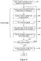
- FIGS. 2A and 2Billustrate high level flow charts for multi-band clipping with example clipping algorithms.
- step 202complex baseband carriers, centered on zero frequency, are input into a clipping stage (steps 203-205 ).
- the input carriersare positioned at a predetermined frequency separation of at least 2CBW, preferably at or near 2CBW.
- predetermined frequency separationis defined as an arbitrary frequency separation of at least 2CBW but also being at most less than the sampling frequency minus 2CBW.
- step 204the positioned carriers are combined into a composite signal.
- the frequency positioning of the carrierscan be performed by complex numerically controlled oscillator (NCO) multiplication and the combination into a composite signal is performed by complex addition of the frequency-shifted carrier signals.
- step 205Aclipping is performed on the composite signal at the predetermined frequency separation, followed by, in step 206 , repositioning the carriers to zero frequency.
- step 207placement to final carrier positions is performed, e.g., to widely separated frequency positions constituting separate operating frequency bands (dual-band or multi-band configurations).
- step 205B of Figure 2Bclipping distortion signal components are added to each carrier of the composite signal e.g., by the method of peak windowing.
- Figure 3is an example diagram of the method shown in Figures 2A and 2B .
- the diagramincludes an upper portion 301 and lower portion 306.
- Upper portion 301illustrates a first carrier band 302 and second carrier band 303 positioned at a predetermined center carrier (CC) separation 305 of at least 2CBW, preferably at or near 2CBW and clipped as combined carriers 304 (composite signal).
- Lower portion 306illustrates the post-clipped carriers, including channel clipping distortion, being repositioned to a dual band separation 307 wider than 2BW (e.g., widely-separated carrier configuration).
- CCcenter carrier
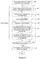
- Figure 4is another example method similar to that illustrated in Figure 2A with two additional steps 406 and 407.
- Step 406recognizes that clipping produces unwanted clipping distortion outside the channel bandwidth (CBW) and removes that distortion by filtering the clip distortion outside the CBW, e.g., with a low pass filter.
- a smoother implementation, in terms of signal reshaping and re-settled amplitudes,may be achieved via step 407 which iteratively performs additional clipping stages.
- FIG. 5illustrates an example implementation using a modification of the Ericsson clipping algorithm.
- the baseband carrierscentered at zero frequency, are input into clipping steps 503-508.
- copies of the input carriersare positioned at a predetermined frequency separation of least 2CBW, preferably at or near 2CBW.
- the positioned carriersare combined into a composite signal.
- clippingis performed on the composite signal at the predetermined frequency separation. Clipping produces clipping distortion, and therefore, in step 506 , the produced clipping distortion is separated out.
- step 507the separated clipping distortion of each carrier is repositioned to zero frequency and clipping distortion outside the channel bandwidth (CBW) filtered with a low pass filter and then in step 508 , the filtered distortion for each carrier is added to input carriers 502.
- step 509iteratively performs additional clipping stages.
- Step 510provides separation of the carriers to carrier positions where they are to be placed in, for example, a widely-separated configuration, with final RF position accomplished through well known methods, such as RF up-conversion or Direct RF up-conversion by use of high speed DACs.
- FIG. 6illustrates a transmitter 600 implementing various stages of the technology described herein.
- Transmittersare well known and consist of many known elements as would be apparent to one skilled in the art. As such, the specific circuitry and power elements will not be described in detail herein.
- the transmitterwill have at least processing circuitry configured as: processing stage 601 , including carrier frequency separation modifier and combiner section 602 and clipping and filtering section 603 , and a multi-carrier bandwidth separation expansion stage 611 .
- the carrier frequency separation modifier and combiner 602include at least a baseband carrier positioner 605, and carrier combiner 606.
- Stage 602implements at least the baseband input, carrier separation, and composite carrier signal functions described above.
- Clipping and filtering stage 603includes a clipping element 607, a baseband carrier positioner 608 , and a filter 609. Additionally, it may also include a clipping distortion separator 607B and an adder 609B. Stage 603 implements at least the clipping and clip distortion handling described above, including repositioning to baseband zero frequency. Stage 611 comprises a tuner 610, for example to separate the carriers to the carrier positions where they are to be placed (e.g., a widely-separated configuration), and provide additional fine tuning of RF position accomplished through well known elements, such as RF up-converter or Direct RF up-converter by use of high speed DACs. In the implementation illustrated in Figures 4 and 5 , processing stage 601 may optionally be iteratively used to provide a smoother implementation in terms of signal reshaping and re-settled amplitudes.
- Figure 7illustrates an example clipping circuit 700 for implementing the method of clipping in Figure 5 with the clip distortion filtered out from a hard clipping stage and confined to the carrier itself.
- copies 701 of baseband versions (i.e. centered at zero frequency) of upper carrier signal 710-U and lower carrier signal 710-Lare frequency shifted 702 to a predetermined frequency and combined together 703 to form a composite signal 711 with a carrier center separation of at least 2BW.
- This composite signalis then clipped in stage 704.
- the clipped peak signalis separated out in 705 and contains the clipping distortion for the carriers which is then shifted back into upper and lower signals centered around zero frequency in stage 706.
- the separated signalsare filtered by low pass filters in stage 707.
- the remaining clipping distortionis added to both the upper carrier 710-U in stage 708 and lower carrier 710-L in stage 709 producing separated carriers 712-U and 712-L with clipping distortion within the carrier band.
- Figure 8illustrates the circuit 700 of Figure 7 replicated in series as three clipping stages 700(1), 700(2), and 700(3) to achieve a smoother implementation as previously described.
- these carriersmay then be placed into their relative frequency positions by analog RF up-conversion in tuner 801 by methods well known to those skilled in the art.
- FIG. 7 and 8The two-band solution as shown in Figures 7 and 8 is equally applicable for three or even more bands.
- Figure 9illustrates a three-band solution.
- Three bands of carrier frequencies 901include additional carrier f3 added to the circuit configuration of Figure 7 .
- One skilled in the art of signal processingcould continue to expand the process to support a multitude of additional bands.
- the circuitalso includes separation of the carriers to the carrier positions where they are to be placed 903 (e.g., in a widely-separated, three band configuration), with final RF position accomplished through well known methods of up-sampling and digital complex frequency tuning.
- a crest factor or peak-to-average ratio (PAR), in the form of a complementary cumulative distribution function (CCDF) curveis compared with the case of high frequency separation.
- PARpeak-to-average ratio
- CCDFcomplementary cumulative distribution function
- Equation 1In order to more clearly see the effect of changing the frequency separation, rearrange Equation 1 and refer all frequencies to the lowest carrier frequency ⁇ 0 - ⁇ /2.
- C te j ⁇ 0 ⁇ ⁇ ⁇ 2 t C 1 t + C 2 t e j ⁇ ⁇ t
- Phasoris defined as a vector representation in the complex plane with the angle to the x-axis corresponding to the phase of the complex signal, and the length of the vector corresponding to the amplitude (or envelope) of the complex signal.
- a phasor representation of C1(t) and C2(t)is shown in figure 10 .
- the argumentis extendable to a larger number of carriers, for example, three carriers as is shown in Equation 3 and figure 11 , or even an arbitrary number of carriers, fulfilling the requirement for enough separation at a reference carrier configuration, where the clipping is performed.
- the reference carrier configurationshould also fulfill the criterion of not placing distortion components from clipping of two of the carrier components into any other (3rd order IM).
- a reference frequencyis now set as the frequency position of the first carrier C1.
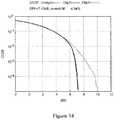
- FIG 12A two carrier example from Matlab simulations of multi-band clipping is shown in figure 12 , figure 13 , and figure 14 .
- Two 20 MHz bandwidth LTE carriersare separated by 44 MHz in a composite configuration, clipped and then separated by 300 MHz in a final dual band configuration.
- Note that the maximum of the envelope in figure 13is essentially the same for the reference configuration and for the final configuration on the time scale of the carrier modulation.
- the CCDFs in figure 14 for the reference configuration (Clip 1) and for the final configuration (Clip 2)are virtually identical as is expected.
- the clipping processnormally involves a hard clipping stage followed by some filtering in order to confine the generated IM products to within the carrier bandwidth (CBW). Without filtering, the third order products will extend out to one CBW on either side of each carrier. Higher order nonlinearities will extend even further out.
- the separation between the carrier edgesneed to be at least one CBW, implying a center-to-center separation of at least 2CBW.
- the separationsshould also be arranged so third order IM products from clipping of two of the carriers do not fall within any other carrier. This is consistent with the result of the Matlab simulations, meaning that higher order nonlinearities than the third have reached sufficiently low levels not to contribute significantly to resulting EVM of each carrier, nor to the crest factor of the combined carrier configuration.
- An example advantage of the method and apparatus described herein for multi-band clippingis that a multitude of clipping algorithms can be extended into multi-band clipping using the technology described herein. Depending on the direct implementation of the clipping algorithm, different adaptations and extensions have to be provided as is well known to one skilled in the art of complex frequency tuning and digital filtering.
- the first stepis to carefully arrange the carriers into a composite configuration with enough spacing between the carriers in order not to allow third order IM products from clipping operations to fall inside the frequency ranges of any of the other carriers or so far outside half the sampling frequency that IM products fold back into any carrier frequency range.
- the total IBW for the reference configuratione.g. 3CBW for a two carrier configuration
- the minimum sampling speed Fse.g. Fs > 5CBW for a two carrier configuration
- the second stepis the placement of the clipped carriers into a multi-band configuration.
- the second advantageis revealed, namely that the required sampling speed for the clipping step is not at all dependent on this second step of setting the actual multi-band configuration, and does not require a sampling speed commensurate with the, often high, IBW for this configuration.
- the clipped signal properties (EVM and EPF) from the first stepare preserved when going from the composite carrier configuration to the actual multi-band configuration.
- the wanted multi-band configurationcan be implemented with any of a number of well known methods (e.g. analog RF up-conversion).
Landscapes
- Engineering & Computer Science (AREA)
- Signal Processing (AREA)
- Computer Networks & Wireless Communication (AREA)
- Transmitters (AREA)
- Reduction Or Emphasis Of Bandwidth Of Signals (AREA)
Description
- The technology relates to signal transmission systems where there is a need to limit the signal peak-to-average power ratio. More specifically, the technology relates to signal peak limitation on widely-separated carriers intended to be transmitted simultaneously. Non-limiting example applications of the technology include telecommunication systems, such as those implementing standards like GSM, WCDMA, LTE or any other standard or combinations thereof.
- Power amplifiers typically are assigned peak power level ratings. One risk is that an amplifier, i.e., normally the main transistor, breaks down if it is exposed to a high peak level. A second risk is that the amplifier itself has a non-linear behavior which may limit high output portions of the signal and include increased emission levels at frequencies outside an intended or allowed spectrum. Reducing power may potentially minimize these particular issues, but will create reduced efficiency levels for the radio equipment. Another example solution includes crest factor reduction (CFR) which can be implemented in a transmitter to reduce peak power in relation to the average power. This can be achieved by directly reducing the peak power by a baseband rearrangement of the baseband signal or by forcing the signal down at peak levels by clipping.
- Clipping can be performed in a baseband signal configuration or on a combined signal. Clipping is a form of distortion that limits a signal once it exceeds a threshold. It may be described as hard, in cases where the signal is strictly limited at the threshold, producing a flat cutoff which results in many high frequency harmonics and intermodulation distortion components.
- In a digital system, the sampling rate for complex signals must be as high as the instantaneous signal bandwidth (IBW) is wide according to the well known Nyquist sampling theorem. Instantaneous signal bandwidth (IBW) is defined as the total bandwidth encompassing all the carriers intended for transmission. Single carrier signals, having a smaller channel bandwidth (CBW), e.g. 5 MHz or 20 MHz, do not require significant signal processing speeds. However, when a signal to be transmitted includes multiple carrier bands separated by a significant frequency bandwidth, for example 20-100 times the channel bandwidth (CBW), instantaneous signal bandwidth quickly becomes a detrimental factor in signal processing speeds.
- Widely-separated carriers, i.e., having a carrier center frequency separation of much greater than twice the channel bandwidth of the carrier bands (>>2CBW), require processing speeds which are not practical for existing hardware. As an example, a widely-separated carrier signal including simultaneous transmission into 3GPP Band 1 (2110-2170 MHz) and Band 7 (2620 - 2690) means a maximum frequency separation of 580 MHz between the bands if an LTE carrier channel bandwidth of 20 MHz is used. Using this example, a matching sampling rate and processing speed of at least 580 MHz would be required, plus an additional spectrum margin. All together, the processing speed would exceed most hardware capabilities currently available.
- Hard clipping of a signal to be transmitted also produces unwanted emissions outside the intended spectrum. Such emissions usually do not comply with requirements set up by standardization bodies. Therefore, filtering is often applied when hard clipping is used to introduce crest factor reduction (CFR) methods. Other CFR methods are also available which do not require hard clipping. For example, an article ofM. R. Schroeder, "Synthesis of low-peak-factor signals and binary sequences with low autocorrelation,"IEEE Transactions on Information Theory, vol. IT-16, pp. 85-89, Jan. 1970, teaches a phase adjustment of each continuous-wave tone (CW-tone) used to decrease the peak-to-average ratio (PAR) of the signal without hard clipping it.
- Clipping can be viewed as if a certain spectrum is added to the original spectrum of isolated carriers just covering the instantaneous bandwidth (IBW) of the carriers. The terms "adding a clipping spectrum" or "adding crest factor reduction signal components" will be used throughout the specification and drawings even though the actual signal amplitudes are limited or decreased by the clipping operation. The tolerated spectrum inside the desired transmission band is usually larger than the unwanted spectrum outside the carriers. Some examples of this are found in the telecom standards defined by 3GPP. Unwanted emissions are defined via specified allowed levels in certain frequency ranges, by adjacent channel leakage power ratio (ACLR, and via a spectrum mask, both defined just outside the channel bandwidth of the carriers. Inside the carriers, the unwanted emission requirement is often converted into an error vector magnitude (EVM) that must be below a certain limit.
- CFR methods essentially address the question of how to compute the necessary extra spectrum that brings the PAR down to a predefined level but at the same time fulfill the requirement of achieving a low EVM figure and low unwanted emissions outside the carriers. Illustrative methods include, but are not limited to: 1) a method developed by Ericsson as described in R. Hellberg, "Apparatuses and a method for reducing peak power in telecommunications systems",
PCT/SE2006/050237 102271105 relates to a broadband IF design method and apparatus to complete DUC spectrum and spectrum shifting.US Patent Publication No. 2005/0118966 relates to a crest factor reduction circuit to boost output power of a multi-career wireless RF amplifier. - All these methods try to satisfy common design goals for EVM and unwanted emissions. The technology described below can be used along with any of these methods, or others, both known and future, to provide crest factor reduction for multi-band signals.
- A common outcome of existing solutions is that combined carriers before and after clipping are the same but also contain some clip distortion. This clip distortion is normally contained inside the carriers, hiding the unwanted spectrum emissions to the carriers. The amount of clip distortion, in relation to the carrier power itself, defines the error vector magnitude (EVM) of the signal. Existing telecommunication standards set a maximum EVM threshold to ensure satisfactory demodulation at the receiver end. This maximum EVM threshold may vary with bit rate and transmission configuration, e.g., supporting MIMO.
- The technology described herein addresses the problem of clipping carriers in a multi-carrier system. As previously described, existing approaches may require a very high sampling speed in order for the method to work over the entire multi-carrier or combined signal. Clipping has to be made on the combined signal to be effective. Separate clipping on individual ones of the multiple carriers at a low speed requires a non-optimal testing step and introduces high signal latency and increased complexity.
- What is needed is a solution that reduces sampling rates required to clip carriers in a multi-carrier system where the sampling speed would be too high for a practical solution to work.
- In an example embodiment, a method and apparatus is disclosed for crest factor reduction (CFR) of a multi-carrier signal, where each carrier of the multi-carrier signal has a respective center frequency and channel bandwidth (CBW). The method and apparatus include elements to position a baseband version of each of the carriers to a first frequency separation between adjacent carriers of at least twice the CBW thereafter, combine the positioned carriers into a composite signal, clip the composite signal, reposition each carrier of the clipped composite signal back into a baseband version centered at zero frequency, and position each carrier at their respective center frequency.
- In one aspect of the example embodiment, after clipping the composite signal, the clipping distortion is separated out, repositioned for each carrier to a baseband version centered at zero frequency, filtered outside each carrier's channel bandwidth and added to the respective base band version of each carrier centered at zero frequency.
- In another aspect of the example embodiment, the clipping is iteratively performed.
- In another aspect of the example embodiment, each carrier of the crest factor reduced multi-carrier signal is repositioned by either analog RF up-conversion, digital complex frequency tuning or by a combination of both at their respective center frequency. The carriers can be grouped into a plurality of frequency bands, each frequency band comprising a single carrier or a plurality of carriers, the edges of the frequency bands being separated in frequency by any value between 0 Hz and several GHz.
- In another aspect of the example embodiment, the multi-carrier signal includes three or more carriers.
Figure 1 is a graph of an exemplary signal format illustrating two carriers that undergo hard clipping.Figures 2A and2B illustrate high level flow charts for multi-band clipping with example clipping algorithms.Figure 3 is a graph of the steps illustrated inFigures 2A and2B including frequency tuning of carriers into final carrier positions.Figure 4 illustrates a modifiedFigure 2A flow chart for multi-band clipping with an example clipping algorithm.Figure 5 illustrates an example implementation using a modification of an Ericsson clipping algorithm.Figure 6 illustrates an example transmitter implementing various stages of the technology described herein.Figure 7 illustrates an example circuit diagram illustrating a single clip stage adding clip distortion to two carriers placed at zero-frequency baseband.Figure 8 illustrates an example circuit diagram illustrating several of the clip stages ofFigure 7 in a cascade formation followed by analog RF up-conversion.Figure 9 illustrates an example circuit diagram illustrating a single clip stage showing added clip distortion to three carriers placed at zero-frequency baseband followed by digital complex frequency tuning positioning each carrier at their respective center frequency.Figure 10 illustrates a phasor representation of carriers C1 and C2 showing phasor C2 rotationrelative C 1 and maximum of combined amplitude.Figure 11 illustrates a phasor representation of carriers C1, C2 and C3 showing phasor C3 rotation relative C2 at maximum of combined amplitude forC 1 and C2.Figure 12 illustrates a graph of carriers C1 and C2 at reference position (center) and at final positions (left and right).Figure 13 illustrates a graph of absolute values of clipped signals at carrier reference position (Clip 1) and at final carrier positions (Clip 2).Figure 14 illustrates a graph of CCDF (Complementary Cumulative Distribution Function) for the clipped signal at reference carrier position (Clip 1) and final carrier positions (Clip 2). Also illustrated is the CCDF for the unclipped signal.- The following description sets forth specific details, such as particular embodiments for purposes of explanation and not limitation. But it will be appreciated by one skilled in the art that other embodiments may be employed apart from these specific details. In some instances, detailed descriptions of well known methods, nodes, interfaces, circuits, and devices are omitted so as not obscure the description with unnecessary detail. Those skilled in the art will appreciate that the functions described may be implemented in radio communications circuitry (e.g. in a transmitter) with a variety of crest factor reduction methods using hardware circuitry (e.g., analog and/or discrete logic gates interconnected to perform a specialized function, ASICs, PLAs, etc.) and/or using software programs and data in conjunction with one or more digital microprocessors or general purpose computers. Moreover, the technology can additionally be considered to be embodied entirely within any form of computers readable memory, such as solid-state memory, magnetic disk, or optical disk containing an appropriate set of computer instructions that would cause a processor to carry out the techniques described herein.
- Hardware implementation may include or encompass, without limitation, digital signal processor (DSP) hardware, a reduced instruction set processor, hardware (e.g., digital or analog) circuitry including but not limited to application specific integrated circuit(s) (ASIC) and/or field programmable gate array(s) (FPGA(s)), and (where appropriate) state machines capable of performing such functions.
- In terms of computer implementation, a computer is generally understood to comprise one or more processors or one or more controllers, and the terms computer, processor, and controller may be employed interchangeably. When provided by a computer, processor, or controller, the functions may be provided by a single dedicated computer or processor or controller, by a single shared computer or processor or controller, or by a plurality of individual computers or processors or controllers, some of which may be shared or distributed. Moreover, the term "processor" or "controller" also refers to other hardware capable of performing such functions and/ or executing software, such as the example hardware recited above.
- Non-limiting example embodiments of the technology described in this application may be used to improve signal quality in any transmission system. The transmission system may be part of an existing or future network using various protocols and noise handling requirements, for example CDMA, WCDMA, HSPA, SCFDMA, OFDMA, LTE, or a mixture thereof, etc.
- Baseband is defined as a signal that has undergone modulation and channeling processing except conversion to an analog signal, upconversion to an RF frequency, and amplification for final transmission by an antenna.
Figure 1 is a graph of an exemplary signal format illustrating a multi-band signal configuration with two carriers (101 and102), separated by a center carrier (CC)frequency separation 106, that undergo hard clipping105 (labeled "raw clipping", i.e., without smoothing).Carriers - An example method and system are now described that eliminate this clipping problem in a multi-band system with widely-separated carriers.
Figures 2A and2B illustrate high level flow charts for multi-band clipping with example clipping algorithms. Instep 202, complex baseband carriers, centered on zero frequency, are input into a clipping stage (steps203-205). (Complex baseband signals is a common nomenclature in digital signal processing and expresses the general property of any signal having a phase and an amplitude (in polar notation) expressed in rectangular (Cartesian) form, i.e., the signal expressed as a combination of having a real part and an imaginary part I + jQ, where the I-part is called the In-phase component and the Q-part is called the Quadrature-phase component.) Instep 203, the input carriers are positioned at a predetermined frequency separation of at least 2CBW, preferably at or near 2CBW. (predetermined frequency separation is defined as an arbitrary frequency separation of at least 2CBW but also being at most less than the sampling frequency minus 2CBW. This constitutes a temporary frequency separation that only exists when calculating the proper clip distortion to be added to each carrier.) Instep 204, the positioned carriers are combined into a composite signal. (The frequency positioning of the carriers can be performed by complex numerically controlled oscillator (NCO) multiplication and the combination into a composite signal is performed by complex addition of the frequency-shifted carrier signals.) Instep 205A, clipping is performed on the composite signal at the predetermined frequency separation, followed by, instep 206, repositioning the carriers to zero frequency. In207, placement to final carrier positions is performed, e.g., to widely separated frequency positions constituting separate operating frequency bands (dual-band or multi-band configurations). The final RF position is accomplished through well known methods, such as RF up-conversion or Direct RF up-conversion by use of high speed DACs. The specific method is not further discussed herein since it does not impact the technology described for multi-band clipping. Instep 205B ofFigure 2B , clipping distortion signal components are added to each carrier of the composite signal e.g., by the method of peak windowing. Figure 3 is an example diagram of the method shown inFigures 2A and2B . The diagram includes anupper portion 301 andlower portion 306.Upper portion 301 illustrates afirst carrier band 302 andsecond carrier band 303 positioned at a predetermined center carrier (CC)separation 305 of at least 2CBW, preferably at or near 2CBW and clipped as combined carriers304 (composite signal).Lower portion 306 illustrates the post-clipped carriers, including channel clipping distortion, being repositioned to adual band separation 307 wider than 2BW (e.g., widely-separated carrier configuration).Figure 4 is another example method similar to that illustrated inFigure 2A with twoadditional steps Step 406, recognizes that clipping produces unwanted clipping distortion outside the channel bandwidth (CBW) and removes that distortion by filtering the clip distortion outside the CBW, e.g., with a low pass filter. A smoother implementation, in terms of signal reshaping and re-settled amplitudes, may be achieved viastep 407 which iteratively performs additional clipping stages.Figure 5 illustrates an example implementation using a modification of the Ericsson clipping algorithm. Instep 502, the baseband carriers, centered at zero frequency, are input into clipping steps503-508. Instep 503, copies of the input carriers are positioned at a predetermined frequency separation of least 2CBW, preferably at or near 2CBW. Instep 504, the positioned carriers are combined into a composite signal. Instep 505, clipping is performed on the composite signal at the predetermined frequency separation. Clipping produces clipping distortion, and therefore, instep 506, the produced clipping distortion is separated out. (The process of clipping distortion being separated out constitutes extracting the remainder when subtracting the clipped signal from the unclipped composite signal.) Instep 507, the separated clipping distortion of each carrier is repositioned to zero frequency and clipping distortion outside the channel bandwidth (CBW) filtered with a low pass filter and then instep 508, the filtered distortion for each carrier is added to inputcarriers 502. To achieve a smoother implementation, in terms of signal reshaping and re-settled amplitudes, step509 iteratively performs additional clipping stages. Step510 provides separation of the carriers to carrier positions where they are to be placed in, for example, a widely-separated configuration, with final RF position accomplished through well known methods, such as RF up-conversion or Direct RF up-conversion by use of high speed DACs.Figure 6 illustrates atransmitter 600 implementing various stages of the technology described herein. Transmitters are well known and consist of many known elements as would be apparent to one skilled in the art. As such, the specific circuitry and power elements will not be described in detail herein. However, in an example implementation, the transmitter will have at least processing circuitry configured as: processingstage 601, including carrier frequency separation modifier andcombiner section 602 and clipping andfiltering section 603, and a multi-carrier bandwidthseparation expansion stage 611. The carrier frequency separation modifier andcombiner 602 include at least abaseband carrier positioner 605, andcarrier combiner 606.Stage 602 implements at least the baseband input, carrier separation, and composite carrier signal functions described above. Clipping andfiltering stage 603 includes aclipping element 607, abaseband carrier positioner 608, and afilter 609. Additionally, it may also include a clipping distortion separator607B and an adder609B.Stage 603 implements at least the clipping and clip distortion handling described above, including repositioning to baseband zero frequency.Stage 611 comprises atuner 610, for example to separate the carriers to the carrier positions where they are to be placed (e.g., a widely-separated configuration), and provide additional fine tuning of RF position accomplished through well known elements, such as RF up-converter or Direct RF up-converter by use of high speed DACs. In the implementation illustrated inFigures 4 and5 ,processing stage 601 may optionally be iteratively used to provide a smoother implementation in terms of signal reshaping and re-settled amplitudes.Figure 7 illustrates anexample clipping circuit 700 for implementing the method of clipping inFigure 5 with the clip distortion filtered out from a hard clipping stage and confined to the carrier itself. In a first stage,copies 701 of baseband versions (i.e. centered at zero frequency) of upper carrier signal710-U and lower carrier signal710-L are frequency shifted702 to a predetermined frequency and combined together703 to form acomposite signal 711 with a carrier center separation of at least 2BW. This composite signal is then clipped instage 704. The clipped peak signal is separated out in705 and contains the clipping distortion for the carriers which is then shifted back into upper and lower signals centered around zero frequency instage 706. The separated signals are filtered by low pass filters instage 707. The remaining clipping distortion is added to both the upper carrier710-U instage 708 and lower carrier710-L instage 709 producing separated carriers712-U and712-L with clipping distortion within the carrier band.Figure 8 illustrates thecircuit 700 ofFigure 7 replicated in series as three clipping stages700(1), 700(2), and700(3) to achieve a smoother implementation as previously described. In this example of two carriers, these carriers may then be placed into their relative frequency positions by analog RF up-conversion intuner 801 by methods well known to those skilled in the art.- The two-band solution as shown in
Figures 7 and8 is equally applicable for three or even more bands. For example,Figure 9 illustrates a three-band solution. Three bands ofcarrier frequencies 901 include additional carrierf3 added to the circuit configuration ofFigure 7 . One skilled in the art of signal processing could continue to expand the process to support a multitude of additional bands. The circuit also includes separation of the carriers to the carrier positions where they are to be placed903 (e.g., in a widely-separated, three band configuration), with final RF position accomplished through well known methods of up-sampling and digital complex frequency tuning. - To show some of the advantages of the technology described herein, an example is presented where two LTE carriers are clipped to a certain value, and a crest factor or peak-to-average ratio (PAR), in the form of a complementary cumulative distribution function (CCDF) curve, is compared with the case of high frequency separation. Initially, the carriers are placed relatively close to each other (e.g. 2BW frequency separation), combined into a composite signal, clipped, and then using the resulting carriers, including their clipping distortion, used to construct two carriers that are widely-separated (>>2CBW).
- An explanation of the theory behind multi-carrier clipping follows. Consider two base band carriersC1(t)=A1(t)ejϕ
1 (t) andC2(t)=A2(t)ejϕ2 (t) whose complex modulation of amplitude and phase is represented by the momentary values of A(t) and ϕ(t). Separating the two carriers by Δω around a center frequency of ω0 gives the following expression for the combined carriers
- Note that it is only the carrier separation Δω and the complex base band modulations C1(t) and C2(t) that affects the total momentary amplitude of the combined carriers, and not the common offset frequency ω0 (also can be set to zero).
- In order to more clearly see the effect of changing the frequency separation, rearrange
Equation 1 and refer all frequencies to the lowest carrier frequency ω0 - Δω/2.
- Ignoring the common offset frequency ω0 - Δω/2, it is clear that it is the carrier separation Δω and the two carriers base band modulations C1(t) and C2(t) that affect the total combined momentary amplitude and C2(t) phasor position relative to the now fixed phasor C1(t). Phasor is defined as a vector representation in the complex plane with the angle to the x-axis corresponding to the phase of the complex signal, and the length of the vector corresponding to the amplitude (or envelope) of the complex signal. A phasor representation of C1(t) and C2(t) is shown in
figure 10 . - It is clear that if Δω is much greater than each carrier bandwidth CBW the phasorejΔωt will rotate much faster than C1(t) will change relative to the phasor C2(t) (also considered stationary on the
time scale 2/CBW). This also means that as long as Δω>> CBW, the actual value of Δω is not important for the maximum combined carrier amplitude max|C| (on thetime scale 2/CBW). - The consequence of this is that, if clipping of the combined carriers (affecting the amplitudes of both C1 and C2) is performed at a reference carrier separation (Δωr), and the carriers are shifted to a new carrier separation (Δωn), the maximum combined carrier amplitude max|C| will not change. This proves that the proposed multi-carrier clipping works for two carriers. The criterion Δω >> CBW is not critical and can, in practice, be relaxed to Δω > 2CBW.
- The argument is extendable to a larger number of carriers, for example, three carriers as is shown in
Equation 3 andfigure 11 , or even an arbitrary number of carriers, fulfilling the requirement for enough separation at a reference carrier configuration, where the clipping is performed. With three or more carriers, the reference carrier configuration should also fulfill the criterion of not placing distortion components from clipping of two of the carrier components into any other (3rd order IM). For the three carrier example below, a reference frequency is now set as the frequency position of the first carrier C1.
- A two carrier example from Matlab simulations of multi-band clipping is shown in
figure 12 ,figure 13 , andfigure 14 . Two 20 MHz bandwidth LTE carriers are separated by 44 MHz in a composite configuration, clipped and then separated by 300 MHz in a final dual band configuration. Note that the maximum of the envelope infigure 13 is essentially the same for the reference configuration and for the final configuration on the time scale of the carrier modulation. The CCDFs infigure 14 for the reference configuration (Clip 1) and for the final configuration (Clip 2) are virtually identical as is expected. - There is also another reason for having enough separation of the carriers in the composite configuration for clipping. The clipping process normally involves a hard clipping stage followed by some filtering in order to confine the generated IM products to within the carrier bandwidth (CBW). Without filtering, the third order products will extend out to one CBW on either side of each carrier. Higher order nonlinearities will extend even further out.
- In order not to have any third order IM products to fall within the next carrier, the separation between the carrier edges need to be at least one CBW, implying a center-to-center separation of at least 2CBW. With three or more carriers, the separations should also be arranged so third order IM products from clipping of two of the carriers do not fall within any other carrier. This is consistent with the result of the Matlab simulations, meaning that higher order nonlinearities than the third have reached sufficiently low levels not to contribute significantly to resulting EVM of each carrier, nor to the crest factor of the combined carrier configuration.
- An example advantage of the method and apparatus described herein for multi-band clipping is that a multitude of clipping algorithms can be extended into multi-band clipping using the technology described herein. Depending on the direct implementation of the clipping algorithm, different adaptations and extensions have to be provided as is well known to one skilled in the art of complex frequency tuning and digital filtering.
- The first step is to carefully arrange the carriers into a composite configuration with enough spacing between the carriers in order not to allow third order IM products from clipping operations to fall inside the frequency ranges of any of the other carriers or so far outside half the sampling frequency that IM products fold back into any carrier frequency range. The total IBW for the reference configuration (e.g. 3CBW for a two carrier configuration) thus sets the minimum sampling speed Fs (e.g. Fs > 5CBW for a two carrier configuration) required for this first step of the multi-band clipping method.
- The second step is the placement of the clipped carriers into a multi-band configuration. Here the second advantage is revealed, namely that the required sampling speed for the clipping step is not at all dependent on this second step of setting the actual multi-band configuration, and does not require a sampling speed commensurate with the, often high, IBW for this configuration. As shown earlier, the clipped signal properties (EVM and EPF) from the first step are preserved when going from the composite carrier configuration to the actual multi-band configuration. The wanted multi-band configuration can be implemented with any of a number of well known methods (e.g. analog RF up-conversion).
- Although various embodiments have been shown and described in detail, the claims are not limited to any particular embodiment or example. None of the above description should be read as implying that any particular element, step, range, or function is essential such that it must be included in the claims scope. The scope of patented subject matter is defined only by the claims. The extent of legal protection is defined by the words recited in the allowed claims and their equivalents. All structural and functional equivalents to the elements of the above-described preferred embodiment that are known to those of ordinary skill in the art are expressly incorporated herein by reference and are intended to be encompassed by the present claims. Moreover, it is not necessary for a device or method to address each and every problem sought to be solved by the technology described, for it to be encompassed by the present claims. Furthermore, no embodiment, feature, component, or step in this specification is intended to be dedicated to the public regardless of whether the embodiment, feature, component, or step is recited in the claims.


Claims (6)
- A method for crest factor reduction (CFR) of a multi-carrier signal, each carrier (101, 102) of the multi-carrier signal having a respective center frequency and a channel bandwidth (CBW), the method comprising:positioning (203) a baseband version of each of the carriers to a frequency separation between adjacent carriers (101, 102) of at least twice the CBW (101, 102),thereafter, combining (204) the positioned carriers (101, 102) into a composite signal,clipping (205A) the composite signal, separating out (506) clipping distortion (103, 104), andrepositioning (206) each carrier (101, 102) of the clipped composite signal back into a baseband version centered at zero frequency, and repositioning the clipping distortion (103, 104) of each carrier of the clipped composite signal back into a baseband version centered at zero frequency;filtering (507) clipping distortion outside each carrier's channel bandwidth, andadding (508) the filtered clipping distortion to the respective base band version of each carrier centered at zero frequency; andpositioning (207) each carrier (101, 102) at their respective center frequency.
- The method according to claim 1, further comprising iteratively applying (509) the method.
- The method according to claim 1, further comprising grouping the center frequencies of the carriers of the crest factor reduced multi-carrier signal into a plurality of frequency bands, each frequency band comprising a single carrier or a plurality of carriers, the edges of the frequency bands being separated in frequency by 0 Hz to several GHz.
- The method according to claim 1, wherein positioning each carrier (101, 102) at their respective center frequency, includes analog RF up-conversion, digital complex frequency tuning, or a combination of both.
- The method according to claim 1, wherein the multi-carrier signal comprises three or more carriers.
- An apparatus (600) for crest factor reduction (CFR) of a multi-carrier signal, each carrier (101, 102) of the multi-carrier signal having a respective center frequency and a channel bandwidth (CBW), the apparatus comprising:first baseband carrier positioning circuitry (605) to position a baseband version of each of the carriers (101, 102) to a frequency separation between adjacent carriers of at least twice the CBW of each carrier (101, 102),a carrier combiner (606) to combine the positioned carriers into a composite signal,clipping circuitry (607) to clip the composite signal, separator circuitry (607B) for separating out clipping distortion (103, 104), andsecond baseband carrier positioning circuitry (608) to reposition each carrier of the clipped composite signal and the clipping distortion (103, 104) of each carrier of the clipped composite signal back into a baseband version centered at zero frequency,filter circuitry (609) to filter clipping distortion outside each carrier's channel bandwidth, adding circuitry (609B) to add the filtered clipping distortion (103, 104) to the respective base band version of each carrier centered at zero frequency;a tuner (610) to reposition each carrier of the clipped composite signal to their respective center frequencies.
Applications Claiming Priority (2)
| Application Number | Priority Date | Filing Date | Title |
|---|---|---|---|
| US13/333,736US9215120B2 (en) | 2011-12-21 | 2011-12-21 | Multi-band crest factor reduction |
| PCT/SE2012/051124WO2013095251A2 (en) | 2011-12-21 | 2012-10-19 | Multi-band crest factor reduction |
Publications (3)
| Publication Number | Publication Date |
|---|---|
| EP2795862A2 EP2795862A2 (en) | 2014-10-29 |
| EP2795862A4 EP2795862A4 (en) | 2015-08-05 |
| EP2795862B1true EP2795862B1 (en) | 2017-07-26 |
Family
ID=48654468
Family Applications (1)
| Application Number | Title | Priority Date | Filing Date |
|---|---|---|---|
| EP12859824.0AActiveEP2795862B1 (en) | 2011-12-21 | 2012-10-19 | Multi-band crest factor reduction |
Country Status (4)
| Country | Link |
|---|---|
| US (1) | US9215120B2 (en) |
| EP (1) | EP2795862B1 (en) |
| IN (1) | IN2014KN01478A (en) |
| WO (1) | WO2013095251A2 (en) |
Families Citing this family (33)
| Publication number | Priority date | Publication date | Assignee | Title |
|---|---|---|---|---|
| US8750174B2 (en)* | 2012-03-30 | 2014-06-10 | Broadcom Corporation | Dual carrier separation |
| US20140169496A1 (en)* | 2012-12-17 | 2014-06-19 | Texas Instruments Incorporated | Crest Factor Reduction for Multi-Band System |
| US9065605B2 (en)* | 2013-03-13 | 2015-06-23 | Futurewei Technologies, Inc. | Methods and systems for crest factor reduction in multi-carrier multi-channel architectures |
| US9331882B2 (en)* | 2013-06-05 | 2016-05-03 | Telefonaktiebolaget L M Ericsson (Publ) | Crest factor reduction of carrier aggregated signals |
| US9236899B2 (en)* | 2013-06-05 | 2016-01-12 | Telefonaktiebolaget L M Ericsson (Publ) | Crest factor reduction of inter-band carrier aggregated signals |
| US8948303B1 (en)* | 2013-11-18 | 2015-02-03 | Microelectronics Technology Inc. | Communication device and method of crest factor reduction using amplitude compression |
| US9331725B2 (en) | 2014-01-03 | 2016-05-03 | Maxlinear, Inc. | Method and system for crest factor reduction |
| CN107078750B (en)* | 2014-10-31 | 2019-03-19 | 瑞典爱立信有限公司 | The method and computer program of invasion signal in radio receiver, detection radio receiver |
| US9806929B2 (en)* | 2014-12-12 | 2017-10-31 | Intel IP Corporation | Communication device with power amplifier crest factor reduction |
| FR3034935B1 (en)* | 2015-04-10 | 2017-05-05 | Thales Sa | METHOD OF REDUCING THE FACTOR CREATED BY MULTICHANNEL TRANSMISSION BY INTELLIGENT AND ADAPTIVE SCREENING / FILTERING |
| US9590668B1 (en) | 2015-11-30 | 2017-03-07 | NanoSemi Technologies | Digital compensator |
| CN107438044B (en) | 2016-05-10 | 2021-09-03 | 恩智浦美国有限公司 | Noise shaping Crest Factor Reduction (CFR) method and apparatus |
| CN107404331B (en)* | 2016-05-13 | 2021-02-05 | 恩智浦美国有限公司 | Method and apparatus for processing digital composite signal |
| WO2018067969A1 (en) | 2016-10-07 | 2018-04-12 | Nanosemi, Inc. | Beam steering digital predistortion |
| WO2018156932A1 (en)* | 2017-02-25 | 2018-08-30 | Nanosemi, Inc. | Multiband digital predistorter |
| US10141961B1 (en) | 2017-05-18 | 2018-11-27 | Nanosemi, Inc. | Passive intermodulation cancellation |
| US10581470B2 (en) | 2017-06-09 | 2020-03-03 | Nanosemi, Inc. | Linearization system |
| US10931318B2 (en)* | 2017-06-09 | 2021-02-23 | Nanosemi, Inc. | Subsampled linearization system |
| US11115067B2 (en) | 2017-06-09 | 2021-09-07 | Nanosemi, Inc. | Multi-band linearization system |
| US11323188B2 (en) | 2017-07-12 | 2022-05-03 | Nanosemi, Inc. | Monitoring systems and methods for radios implemented with digital predistortion |
| EP3669461A1 (en) | 2017-08-17 | 2020-06-24 | Telefonaktiebolaget LM Ericsson (Publ) | Coherent multi band peak detection |
| US11303251B2 (en) | 2017-10-02 | 2022-04-12 | Nanosemi, Inc. | Digital predistortion adjustment based on determination of load condition characteristics |
| CN111971914B (en)* | 2018-04-08 | 2023-02-03 | 上海诺基亚贝尔股份有限公司 | Wireless data transmission |
| US10644657B1 (en) | 2018-05-11 | 2020-05-05 | Nanosemi, Inc. | Multi-band digital compensator for a non-linear system |
| KR20210008073A (en) | 2018-05-11 | 2021-01-20 | 나노세미, 인크. | Digital compensator for nonlinear systems |
| KR20210013714A (en) | 2018-05-25 | 2021-02-05 | 나노세미, 인크. | Digital predistortion under changing operating conditions |
| US10931238B2 (en) | 2018-05-25 | 2021-02-23 | Nanosemi, Inc. | Linearization with envelope tracking or average power tracking |
| US11863210B2 (en) | 2018-05-25 | 2024-01-02 | Nanosemi, Inc. | Linearization with level tracking |
| US10594530B2 (en)* | 2018-05-29 | 2020-03-17 | Qualcomm Incorporated | Techniques for successive peak reduction crest factor reduction |
| FI20195895A1 (en) | 2019-10-16 | 2021-04-17 | Nokia Solutions & Networks Oy | Distribution of clipping noise between bands |
| US10992326B1 (en) | 2020-05-19 | 2021-04-27 | Nanosemi, Inc. | Buffer management for adaptive digital predistortion |
| US11619662B1 (en)* | 2021-09-17 | 2023-04-04 | Rohde & Schwarz Gmbh & Co. Kg | Measurement system and method for a parallel measurement with multiple tones |
| US20250112812A1 (en)* | 2023-09-28 | 2025-04-03 | Apple Inc. | Crest factor reduction systems and methods |
Family Cites Families (16)
| Publication number | Priority date | Publication date | Assignee | Title |
|---|---|---|---|---|
| SE513863C2 (en)* | 1999-01-29 | 2000-11-20 | Ericsson Telefon Ab L M | Method and apparatus for cutting in a CDMA system |
| US6570929B1 (en) | 1999-07-08 | 2003-05-27 | Telefonaktiebolaget Lm Ericsson (Publ) | Power control scheme for maximizing carrier signal-to-noise ratio in multicarrier transmitters |
| US6754285B1 (en)* | 2000-08-01 | 2004-06-22 | Centillium Communications, Inc. | Signal conditioning techniques in DMT-based transmissions |
| US7058004B2 (en)* | 2001-05-07 | 2006-06-06 | University Of South Florida | Communication system using orthogonal wavelet division multiplexing (OWDM) and OWDM-spread spectrum (OWSS) signaling |
| US7266354B2 (en) | 2001-06-25 | 2007-09-04 | Telefonaktiebolaget Lm Ericsson (Publ) | Reducing the peak-to-average power ratio of a communication signal |
| EP1331743A1 (en) | 2002-01-18 | 2003-07-30 | Alcatel | A method and an electronic circuit for clipping of signals, especially CDMA or OFDM signals, with multiple inputs and outputs |
| US7697591B2 (en)* | 2002-08-26 | 2010-04-13 | Texas Instruments Incorporated | Crest factor reduction processor for wireless communications |
| US20050118966A1 (en) | 2003-12-01 | 2005-06-02 | Kiomars Anvari | Simple Crest Factor reduction technique for multi-carrier signals |
| US7362819B2 (en)* | 2004-06-16 | 2008-04-22 | Lucent Technologies Inc. | Device and method for reducing peaks of a composite signal |
| US7313373B1 (en) | 2005-04-21 | 2007-12-25 | Xilinx, Inc. | Crest factor reduction for use in a multiband transmitter |
| US7792200B2 (en) | 2005-11-14 | 2010-09-07 | Telefonaltiebolaget Lm Ericsson (Publ) | Peak-to-average power reduction |
| DE602006001356D1 (en) | 2006-02-06 | 2008-07-10 | Alcatel Lucent | Modular multiband, multi-standard transceiver circuit for mobile and base stations of radio communication systems |
| JP5016035B2 (en) | 2006-07-03 | 2012-09-05 | テレフオンアクチーボラゲット エル エム エリクソン(パブル) | Apparatus and method for reducing peak power in a communication system |
| US7848446B2 (en) | 2006-09-27 | 2010-12-07 | Telefonaktiebolaget L M Ericsson (Publ) | Reduction of peak-to-average-power ratio in a telecommunications system |
| US8068558B2 (en) | 2008-12-17 | 2011-11-29 | Nortel Networks Limited | Selective peak power reduction |
| CN102271105A (en) | 2010-06-04 | 2011-12-07 | 电信科学技术研究院 | Intermediate frequency design method and device of broadband |
- 2011
- 2011-12-21USUS13/333,736patent/US9215120B2/enactiveActive
- 2012
- 2012-10-19EPEP12859824.0Apatent/EP2795862B1/enactiveActive
- 2012-10-19WOPCT/SE2012/051124patent/WO2013095251A2/enactiveApplication Filing
- 2012-10-19ININ1478KON2014patent/IN2014KN01478A/enunknown
Non-Patent Citations (1)
| Title |
|---|
| None* |
Also Published As
| Publication number | Publication date |
|---|---|
| EP2795862A2 (en) | 2014-10-29 |
| US9215120B2 (en) | 2015-12-15 |
| WO2013095251A3 (en) | 2013-11-07 |
| WO2013095251A2 (en) | 2013-06-27 |
| IN2014KN01478A (en) | 2015-10-23 |
| US20130163512A1 (en) | 2013-06-27 |
| EP2795862A4 (en) | 2015-08-05 |
Similar Documents
| Publication | Publication Date | Title |
|---|---|---|
| EP2795862B1 (en) | Multi-band crest factor reduction | |
| CN101068233B (en) | Method and device for reducing signal peak-to-average power ratio | |
| EP2721790B1 (en) | Multi-carrier peak power reduction in frequency hopping systems | |
| JP2016538761A (en) | Reduced bandwidth of signal in envelope path for envelope tracking system | |
| CN101702698B (en) | Transmitter | |
| US8743981B2 (en) | Modulation method and apparatus | |
| CA2842006C (en) | Multi-band peak power reduction | |
| EP3360260B1 (en) | Crest factor reduction in a radio transmitter | |
| US20250047431A1 (en) | Method, apparatus and computer program | |
| CN101601247A (en) | Be used for producing signal so that reduce the apparatus and method of the peak-to-average force ratio of multicarrier system | |
| CN106664179A (en) | Crest factor reduction of carrier aggregated signals | |
| EP3206300B1 (en) | Outphasing amplifier | |
| US20190349157A1 (en) | Receiver, transmitter, communication system for subband communication and methods for subband communication | |
| US20060120479A1 (en) | System and method for crest factor reduction | |
| US11139781B2 (en) | Power amplifiers | |
| WO2010139095A1 (en) | Method of and base station for reducing peak - to - average power ratio for a multicarrier transmission | |
| EP3042478B1 (en) | Method and apparatus for application of distortion shaping when using peak-to-average ratio reduction | |
| US11102035B1 (en) | Method and apparatus for envelope shaping of multi-carrier signal in envelope tracking transmission | |
| US11569890B2 (en) | Power scaling of transmission signal during transmission beam change | |
| CN100555891C (en) | Transmitter and receiver | |
| US9479374B1 (en) | Digital front-end channelization device | |
| US11750433B2 (en) | Crest factor reduction | |
| Nair et al. | Effects of digital predistortion and crest factor reduction techniques on efficiency and linearity trade-off in class AB GaN-PA | |
| KR20230102358A (en) | Apparatus for improving of transmitter signal flatness of ofdm transmitter using wide signal bandwidth |
Legal Events
| Date | Code | Title | Description |
|---|---|---|---|
| PUAI | Public reference made under article 153(3) epc to a published international application that has entered the european phase | Free format text:ORIGINAL CODE: 0009012 | |
| 17P | Request for examination filed | Effective date:20140612 | |
| AK | Designated contracting states | Kind code of ref document:A2 Designated state(s):AL AT BE BG CH CY CZ DE DK EE ES FI FR GB GR HR HU IE IS IT LI LT LU LV MC MK MT NL NO PL PT RO RS SE SI SK SM TR | |
| DAX | Request for extension of the european patent (deleted) | ||
| A4 | Supplementary search report drawn up and despatched | Effective date:20150703 | |
| RIC1 | Information provided on ipc code assigned before grant | Ipc:H04L 27/26 20060101AFI20150629BHEP | |
| 17Q | First examination report despatched | Effective date:20150710 | |
| GRAP | Despatch of communication of intention to grant a patent | Free format text:ORIGINAL CODE: EPIDOSNIGR1 | |
| STAA | Information on the status of an ep patent application or granted ep patent | Free format text:STATUS: GRANT OF PATENT IS INTENDED | |
| INTG | Intention to grant announced | Effective date:20170511 | |
| RIC1 | Information provided on ipc code assigned before grant | Ipc:H04B 1/00 20060101ALN20170428BHEP Ipc:H04L 5/00 20060101ALI20170428BHEP Ipc:H04L 27/26 20060101AFI20170428BHEP | |
| GRAS | Grant fee paid | Free format text:ORIGINAL CODE: EPIDOSNIGR3 | |
| GRAA | (expected) grant | Free format text:ORIGINAL CODE: 0009210 | |
| STAA | Information on the status of an ep patent application or granted ep patent | Free format text:STATUS: THE PATENT HAS BEEN GRANTED | |
| AK | Designated contracting states | Kind code of ref document:B1 Designated state(s):AL AT BE BG CH CY CZ DE DK EE ES FI FR GB GR HR HU IE IS IT LI LT LU LV MC MK MT NL NO PL PT RO RS SE SI SK SM TR | |
| REG | Reference to a national code | Ref country code:GB Ref legal event code:FG4D | |
| REG | Reference to a national code | Ref country code:CH Ref legal event code:EP | |
| REG | Reference to a national code | Ref country code:AT Ref legal event code:REF Ref document number:913238 Country of ref document:AT Kind code of ref document:T Effective date:20170815 | |
| REG | Reference to a national code | Ref country code:IE Ref legal event code:FG4D | |
| REG | Reference to a national code | Ref country code:DE Ref legal event code:R096 Ref document number:602012035157 Country of ref document:DE | |
| REG | Reference to a national code | Ref country code:NL Ref legal event code:MP Effective date:20170726 | |
| REG | Reference to a national code | Ref country code:LT Ref legal event code:MG4D | |
| REG | Reference to a national code | Ref country code:AT Ref legal event code:MK05 Ref document number:913238 Country of ref document:AT Kind code of ref document:T Effective date:20170726 | |
| PG25 | Lapsed in a contracting state [announced via postgrant information from national office to epo] | Ref country code:AT Free format text:LAPSE BECAUSE OF FAILURE TO SUBMIT A TRANSLATION OF THE DESCRIPTION OR TO PAY THE FEE WITHIN THE PRESCRIBED TIME-LIMIT Effective date:20170726 Ref country code:SE Free format text:LAPSE BECAUSE OF FAILURE TO SUBMIT A TRANSLATION OF THE DESCRIPTION OR TO PAY THE FEE WITHIN THE PRESCRIBED TIME-LIMIT Effective date:20170726 Ref country code:HR Free format text:LAPSE BECAUSE OF FAILURE TO SUBMIT A TRANSLATION OF THE DESCRIPTION OR TO PAY THE FEE WITHIN THE PRESCRIBED TIME-LIMIT Effective date:20170726 Ref country code:NO Free format text:LAPSE BECAUSE OF FAILURE TO SUBMIT A TRANSLATION OF THE DESCRIPTION OR TO PAY THE FEE WITHIN THE PRESCRIBED TIME-LIMIT Effective date:20171026 Ref country code:FI Free format text:LAPSE BECAUSE OF FAILURE TO SUBMIT A TRANSLATION OF THE DESCRIPTION OR TO PAY THE FEE WITHIN THE PRESCRIBED TIME-LIMIT Effective date:20170726 Ref country code:LT Free format text:LAPSE BECAUSE OF FAILURE TO SUBMIT A TRANSLATION OF THE DESCRIPTION OR TO PAY THE FEE WITHIN THE PRESCRIBED TIME-LIMIT Effective date:20170726 Ref country code:NL Free format text:LAPSE BECAUSE OF FAILURE TO SUBMIT A TRANSLATION OF THE DESCRIPTION OR TO PAY THE FEE WITHIN THE PRESCRIBED TIME-LIMIT Effective date:20170726 | |
| PG25 | Lapsed in a contracting state [announced via postgrant information from national office to epo] | Ref country code:ES Free format text:LAPSE BECAUSE OF FAILURE TO SUBMIT A TRANSLATION OF THE DESCRIPTION OR TO PAY THE FEE WITHIN THE PRESCRIBED TIME-LIMIT Effective date:20170726 Ref country code:LV Free format text:LAPSE BECAUSE OF FAILURE TO SUBMIT A TRANSLATION OF THE DESCRIPTION OR TO PAY THE FEE WITHIN THE PRESCRIBED TIME-LIMIT Effective date:20170726 Ref country code:GR Free format text:LAPSE BECAUSE OF FAILURE TO SUBMIT A TRANSLATION OF THE DESCRIPTION OR TO PAY THE FEE WITHIN THE PRESCRIBED TIME-LIMIT Effective date:20171027 Ref country code:IS Free format text:LAPSE BECAUSE OF FAILURE TO SUBMIT A TRANSLATION OF THE DESCRIPTION OR TO PAY THE FEE WITHIN THE PRESCRIBED TIME-LIMIT Effective date:20171126 Ref country code:RS Free format text:LAPSE BECAUSE OF FAILURE TO SUBMIT A TRANSLATION OF THE DESCRIPTION OR TO PAY THE FEE WITHIN THE PRESCRIBED TIME-LIMIT Effective date:20170726 Ref country code:BG Free format text:LAPSE BECAUSE OF FAILURE TO SUBMIT A TRANSLATION OF THE DESCRIPTION OR TO PAY THE FEE WITHIN THE PRESCRIBED TIME-LIMIT Effective date:20171026 Ref country code:PL Free format text:LAPSE BECAUSE OF FAILURE TO SUBMIT A TRANSLATION OF THE DESCRIPTION OR TO PAY THE FEE WITHIN THE PRESCRIBED TIME-LIMIT Effective date:20170726 | |
| PG25 | Lapsed in a contracting state [announced via postgrant information from national office to epo] | Ref country code:DK Free format text:LAPSE BECAUSE OF FAILURE TO SUBMIT A TRANSLATION OF THE DESCRIPTION OR TO PAY THE FEE WITHIN THE PRESCRIBED TIME-LIMIT Effective date:20170726 Ref country code:RO Free format text:LAPSE BECAUSE OF FAILURE TO SUBMIT A TRANSLATION OF THE DESCRIPTION OR TO PAY THE FEE WITHIN THE PRESCRIBED TIME-LIMIT Effective date:20170726 Ref country code:CZ Free format text:LAPSE BECAUSE OF FAILURE TO SUBMIT A TRANSLATION OF THE DESCRIPTION OR TO PAY THE FEE WITHIN THE PRESCRIBED TIME-LIMIT Effective date:20170726 | |
| REG | Reference to a national code | Ref country code:DE Ref legal event code:R097 Ref document number:602012035157 Country of ref document:DE | |
| PG25 | Lapsed in a contracting state [announced via postgrant information from national office to epo] | Ref country code:IT Free format text:LAPSE BECAUSE OF FAILURE TO SUBMIT A TRANSLATION OF THE DESCRIPTION OR TO PAY THE FEE WITHIN THE PRESCRIBED TIME-LIMIT Effective date:20170726 Ref country code:EE Free format text:LAPSE BECAUSE OF FAILURE TO SUBMIT A TRANSLATION OF THE DESCRIPTION OR TO PAY THE FEE WITHIN THE PRESCRIBED TIME-LIMIT Effective date:20170726 Ref country code:MC Free format text:LAPSE BECAUSE OF FAILURE TO SUBMIT A TRANSLATION OF THE DESCRIPTION OR TO PAY THE FEE WITHIN THE PRESCRIBED TIME-LIMIT Effective date:20170726 Ref country code:SM Free format text:LAPSE BECAUSE OF FAILURE TO SUBMIT A TRANSLATION OF THE DESCRIPTION OR TO PAY THE FEE WITHIN THE PRESCRIBED TIME-LIMIT Effective date:20170726 Ref country code:SK Free format text:LAPSE BECAUSE OF FAILURE TO SUBMIT A TRANSLATION OF THE DESCRIPTION OR TO PAY THE FEE WITHIN THE PRESCRIBED TIME-LIMIT Effective date:20170726 | |
| REG | Reference to a national code | Ref country code:CH Ref legal event code:PL | |
| PLBE | No opposition filed within time limit | Free format text:ORIGINAL CODE: 0009261 | |
| STAA | Information on the status of an ep patent application or granted ep patent | Free format text:STATUS: NO OPPOSITION FILED WITHIN TIME LIMIT | |
| 26N | No opposition filed | Effective date:20180430 | |
| REG | Reference to a national code | Ref country code:IE Ref legal event code:MM4A | |
| REG | Reference to a national code | Ref country code:FR Ref legal event code:ST Effective date:20180629 | |
| PG25 | Lapsed in a contracting state [announced via postgrant information from national office to epo] | Ref country code:CH Free format text:LAPSE BECAUSE OF NON-PAYMENT OF DUE FEES Effective date:20171031 Ref country code:LU Free format text:LAPSE BECAUSE OF NON-PAYMENT OF DUE FEES Effective date:20171019 Ref country code:LI Free format text:LAPSE BECAUSE OF NON-PAYMENT OF DUE FEES Effective date:20171031 | |
| REG | Reference to a national code | Ref country code:BE Ref legal event code:MM Effective date:20171031 | |
| PG25 | Lapsed in a contracting state [announced via postgrant information from national office to epo] | Ref country code:BE Free format text:LAPSE BECAUSE OF NON-PAYMENT OF DUE FEES Effective date:20171031 Ref country code:FR Free format text:LAPSE BECAUSE OF NON-PAYMENT OF DUE FEES Effective date:20171031 Ref country code:SI Free format text:LAPSE BECAUSE OF FAILURE TO SUBMIT A TRANSLATION OF THE DESCRIPTION OR TO PAY THE FEE WITHIN THE PRESCRIBED TIME-LIMIT Effective date:20170726 | |
| PG25 | Lapsed in a contracting state [announced via postgrant information from national office to epo] | Ref country code:MT Free format text:LAPSE BECAUSE OF NON-PAYMENT OF DUE FEES Effective date:20171019 | |
| PG25 | Lapsed in a contracting state [announced via postgrant information from national office to epo] | Ref country code:IE Free format text:LAPSE BECAUSE OF NON-PAYMENT OF DUE FEES Effective date:20171019 | |
| PG25 | Lapsed in a contracting state [announced via postgrant information from national office to epo] | Ref country code:HU Free format text:LAPSE BECAUSE OF FAILURE TO SUBMIT A TRANSLATION OF THE DESCRIPTION OR TO PAY THE FEE WITHIN THE PRESCRIBED TIME-LIMIT; INVALID AB INITIO Effective date:20121019 | |
| PG25 | Lapsed in a contracting state [announced via postgrant information from national office to epo] | Ref country code:CY Free format text:LAPSE BECAUSE OF FAILURE TO SUBMIT A TRANSLATION OF THE DESCRIPTION OR TO PAY THE FEE WITHIN THE PRESCRIBED TIME-LIMIT Effective date:20170726 | |
| PG25 | Lapsed in a contracting state [announced via postgrant information from national office to epo] | Ref country code:MK Free format text:LAPSE BECAUSE OF FAILURE TO SUBMIT A TRANSLATION OF THE DESCRIPTION OR TO PAY THE FEE WITHIN THE PRESCRIBED TIME-LIMIT Effective date:20170726 | |
| PG25 | Lapsed in a contracting state [announced via postgrant information from national office to epo] | Ref country code:TR Free format text:LAPSE BECAUSE OF FAILURE TO SUBMIT A TRANSLATION OF THE DESCRIPTION OR TO PAY THE FEE WITHIN THE PRESCRIBED TIME-LIMIT Effective date:20170726 | |
| PG25 | Lapsed in a contracting state [announced via postgrant information from national office to epo] | Ref country code:PT Free format text:LAPSE BECAUSE OF FAILURE TO SUBMIT A TRANSLATION OF THE DESCRIPTION OR TO PAY THE FEE WITHIN THE PRESCRIBED TIME-LIMIT Effective date:20170726 | |
| PG25 | Lapsed in a contracting state [announced via postgrant information from national office to epo] | Ref country code:AL Free format text:LAPSE BECAUSE OF FAILURE TO SUBMIT A TRANSLATION OF THE DESCRIPTION OR TO PAY THE FEE WITHIN THE PRESCRIBED TIME-LIMIT Effective date:20170726 | |
| PGFP | Annual fee paid to national office [announced via postgrant information from national office to epo] | Ref country code:DE Payment date:20241029 Year of fee payment:13 | |
| PGFP | Annual fee paid to national office [announced via postgrant information from national office to epo] | Ref country code:GB Payment date:20241028 Year of fee payment:13 |