EP2795783B1 - System and method for controlling an energy storage device - Google Patents
System and method for controlling an energy storage deviceDownload PDFInfo
- Publication number
- EP2795783B1 EP2795783B1EP12784516.2AEP12784516AEP2795783B1EP 2795783 B1EP2795783 B1EP 2795783B1EP 12784516 AEP12784516 AEP 12784516AEP 2795783 B1EP2795783 B1EP 2795783B1
- Authority
- EP
- European Patent Office
- Prior art keywords
- energy storage
- energy supply
- reference signals
- voltage
- energy
- Prior art date
- Legal status (The legal status is an assumption and is not a legal conclusion. Google has not performed a legal analysis and makes no representation as to the accuracy of the status listed.)
- Active
Links
- 238000004146energy storageMethods0.000titleclaimsdescription135
- 238000000034methodMethods0.000titleclaimsdescription39
- 230000008878couplingEffects0.000claimsdescription74
- 238000010168coupling processMethods0.000claimsdescription74
- 238000005859coupling reactionMethods0.000claimsdescription74
- 210000000352storage cellAnatomy0.000claimsdescription25
- 230000036961partial effectEffects0.000claimsdescription21
- 230000010363phase shiftEffects0.000claimsdescription8
- 230000000737periodic effectEffects0.000claimsdescription6
- 239000013598vectorSubstances0.000description22
- 238000011217control strategyMethods0.000description18
- 238000010586diagramMethods0.000description8
- 210000004027cellAnatomy0.000description7
- 230000002829reductive effectEffects0.000description5
- 230000000903blocking effectEffects0.000description4
- 238000005516engineering processMethods0.000description2
- 230000004913activationEffects0.000description1
- 238000006243chemical reactionMethods0.000description1
- 230000007423decreaseEffects0.000description1
- 230000002950deficientEffects0.000description1
- 230000001419dependent effectEffects0.000description1
- 230000002349favourable effectEffects0.000description1
- 229910001416lithium ionInorganic materials0.000description1
- 230000000717retained effectEffects0.000description1
- 230000002441reversible effectEffects0.000description1
- 239000004065semiconductorSubstances0.000description1
- 230000003068static effectEffects0.000description1
- 230000001960triggered effectEffects0.000description1
Images


Classifications
- B—PERFORMING OPERATIONS; TRANSPORTING
- B60—VEHICLES IN GENERAL
- B60L—PROPULSION OF ELECTRICALLY-PROPELLED VEHICLES; SUPPLYING ELECTRIC POWER FOR AUXILIARY EQUIPMENT OF ELECTRICALLY-PROPELLED VEHICLES; ELECTRODYNAMIC BRAKE SYSTEMS FOR VEHICLES IN GENERAL; MAGNETIC SUSPENSION OR LEVITATION FOR VEHICLES; MONITORING OPERATING VARIABLES OF ELECTRICALLY-PROPELLED VEHICLES; ELECTRIC SAFETY DEVICES FOR ELECTRICALLY-PROPELLED VEHICLES
- B60L58/00—Methods or circuit arrangements for monitoring or controlling batteries or fuel cells, specially adapted for electric vehicles
- B60L58/10—Methods or circuit arrangements for monitoring or controlling batteries or fuel cells, specially adapted for electric vehicles for monitoring or controlling batteries
- B60L58/18—Methods or circuit arrangements for monitoring or controlling batteries or fuel cells, specially adapted for electric vehicles for monitoring or controlling batteries of two or more battery modules
- B60L58/21—Methods or circuit arrangements for monitoring or controlling batteries or fuel cells, specially adapted for electric vehicles for monitoring or controlling batteries of two or more battery modules having the same nominal voltage
- H—ELECTRICITY
- H02—GENERATION; CONVERSION OR DISTRIBUTION OF ELECTRIC POWER
- H02J—CIRCUIT ARRANGEMENTS OR SYSTEMS FOR SUPPLYING OR DISTRIBUTING ELECTRIC POWER; SYSTEMS FOR STORING ELECTRIC ENERGY
- H02J7/00—Circuit arrangements for charging or depolarising batteries or for supplying loads from batteries
- H02J7/0013—Circuit arrangements for charging or depolarising batteries or for supplying loads from batteries acting upon several batteries simultaneously or sequentially
- H02J7/0024—Parallel/serial switching of connection of batteries to charge or load circuit
- H—ELECTRICITY
- H02—GENERATION; CONVERSION OR DISTRIBUTION OF ELECTRIC POWER
- H02M—APPARATUS FOR CONVERSION BETWEEN AC AND AC, BETWEEN AC AND DC, OR BETWEEN DC AND DC, AND FOR USE WITH MAINS OR SIMILAR POWER SUPPLY SYSTEMS; CONVERSION OF DC OR AC INPUT POWER INTO SURGE OUTPUT POWER; CONTROL OR REGULATION THEREOF
- H02M7/00—Conversion of AC power input into DC power output; Conversion of DC power input into AC power output
- H02M7/42—Conversion of DC power input into AC power output without possibility of reversal
- H02M7/44—Conversion of DC power input into AC power output without possibility of reversal by static converters
- H02M7/48—Conversion of DC power input into AC power output without possibility of reversal by static converters using discharge tubes with control electrode or semiconductor devices with control electrode
- H02M7/483—Converters with outputs that each can have more than two voltages levels
- H02M7/4835—Converters with outputs that each can have more than two voltages levels comprising two or more cells, each including a switchable capacitor, the capacitors having a nominal charge voltage which corresponds to a given fraction of the input voltage, and the capacitors being selectively connected in series to determine the instantaneous output voltage
- H—ELECTRICITY
- H02—GENERATION; CONVERSION OR DISTRIBUTION OF ELECTRIC POWER
- H02M—APPARATUS FOR CONVERSION BETWEEN AC AND AC, BETWEEN AC AND DC, OR BETWEEN DC AND DC, AND FOR USE WITH MAINS OR SIMILAR POWER SUPPLY SYSTEMS; CONVERSION OF DC OR AC INPUT POWER INTO SURGE OUTPUT POWER; CONTROL OR REGULATION THEREOF
- H02M7/00—Conversion of AC power input into DC power output; Conversion of DC power input into AC power output
- H02M7/42—Conversion of DC power input into AC power output without possibility of reversal
- H02M7/44—Conversion of DC power input into AC power output without possibility of reversal by static converters
- H02M7/48—Conversion of DC power input into AC power output without possibility of reversal by static converters using discharge tubes with control electrode or semiconductor devices with control electrode
- H02M7/483—Converters with outputs that each can have more than two voltages levels
- H02M7/49—Combination of the output voltage waveforms of a plurality of converters
- H—ELECTRICITY
- H02—GENERATION; CONVERSION OR DISTRIBUTION OF ELECTRIC POWER
- H02J—CIRCUIT ARRANGEMENTS OR SYSTEMS FOR SUPPLYING OR DISTRIBUTING ELECTRIC POWER; SYSTEMS FOR STORING ELECTRIC ENERGY
- H02J2207/00—Indexing scheme relating to details of circuit arrangements for charging or depolarising batteries or for supplying loads from batteries
- H02J2207/20—Charging or discharging characterised by the power electronics converter
- H—ELECTRICITY
- H02—GENERATION; CONVERSION OR DISTRIBUTION OF ELECTRIC POWER
- H02M—APPARATUS FOR CONVERSION BETWEEN AC AND AC, BETWEEN AC AND DC, OR BETWEEN DC AND DC, AND FOR USE WITH MAINS OR SIMILAR POWER SUPPLY SYSTEMS; CONVERSION OF DC OR AC INPUT POWER INTO SURGE OUTPUT POWER; CONTROL OR REGULATION THEREOF
- H02M7/00—Conversion of AC power input into DC power output; Conversion of DC power input into AC power output
- H02M7/42—Conversion of DC power input into AC power output without possibility of reversal
- H02M7/44—Conversion of DC power input into AC power output without possibility of reversal by static converters
- H02M7/48—Conversion of DC power input into AC power output without possibility of reversal by static converters using discharge tubes with control electrode or semiconductor devices with control electrode
- H02M7/53—Conversion of DC power input into AC power output without possibility of reversal by static converters using discharge tubes with control electrode or semiconductor devices with control electrode using devices of a triode or transistor type requiring continuous application of a control signal
- H02M7/537—Conversion of DC power input into AC power output without possibility of reversal by static converters using discharge tubes with control electrode or semiconductor devices with control electrode using devices of a triode or transistor type requiring continuous application of a control signal using semiconductor devices only, e.g. single switched pulse inverters
- H02M7/539—Conversion of DC power input into AC power output without possibility of reversal by static converters using discharge tubes with control electrode or semiconductor devices with control electrode using devices of a triode or transistor type requiring continuous application of a control signal using semiconductor devices only, e.g. single switched pulse inverters with automatic control of output wave form or frequency
- H02M7/5395—Conversion of DC power input into AC power output without possibility of reversal by static converters using discharge tubes with control electrode or semiconductor devices with control electrode using devices of a triode or transistor type requiring continuous application of a control signal using semiconductor devices only, e.g. single switched pulse inverters with automatic control of output wave form or frequency by pulse-width modulation
- Y—GENERAL TAGGING OF NEW TECHNOLOGICAL DEVELOPMENTS; GENERAL TAGGING OF CROSS-SECTIONAL TECHNOLOGIES SPANNING OVER SEVERAL SECTIONS OF THE IPC; TECHNICAL SUBJECTS COVERED BY FORMER USPC CROSS-REFERENCE ART COLLECTIONS [XRACs] AND DIGESTS
- Y02—TECHNOLOGIES OR APPLICATIONS FOR MITIGATION OR ADAPTATION AGAINST CLIMATE CHANGE
- Y02T—CLIMATE CHANGE MITIGATION TECHNOLOGIES RELATED TO TRANSPORTATION
- Y02T10/00—Road transport of goods or passengers
- Y02T10/60—Other road transportation technologies with climate change mitigation effect
- Y02T10/70—Energy storage systems for electromobility, e.g. batteries
Definitions
- the inventionrelates to a system and a method for controlling an energy storage device, in particular in a battery direct converter circuit for generating an n-phase AC voltage.
- the feeding of multiphase current into an electrical machineis usually accomplished by a converter in the form of a pulse-controlled inverter.
- a DC voltage provided by a DC voltage intermediate circuitcan be converted into a multi-phase AC voltage, for example a three-phase AC voltage.
- the DC voltage intermediate circuitis fed by a string of battery modules connected in series. In order to be able to meet the performance and energy requirements for a particular application, several battery modules are often connected in series in a traction battery.
- the coupling unitcan be designed in such a way that it additionally allows the respectively assigned at least one battery cell to be switched into the respective energy storage module line with inverse polarity or also to interrupt the respective energy storage module line.
- suitable phase signalscan also be provided for controlling the phase output voltage, so that a separate pulse inverter can be dispensed with. The pulse inverter required to control the phase output voltage is thus integrated into the BDI, so to speak.
- BDIsare usually more efficient and more reliable than conventional systems.
- the reliabilityis guaranteed, among other things, by the fact that defective, failed or not fully efficient battery cells can be switched out of the energy supply lines by suitable bridging control of the coupling units.
- the phase output voltage of an energy storage module stringcan be varied by appropriate activation of the coupling units and in particular can be set in stages. The gradation of the output voltage results from the voltage of an individual energy storage module, the maximum possible phase output voltage determining the sum of the voltages of all energy storage modules of an energy storage module string.
- a pulse width modulated (PWM) control of the coupling unitscan be carried out to set an output voltage of an energy storage module. This makes it possible to output a desired mean value as an energy storage module voltage by specifically varying the switch-on and switch-off times.
- PWMpulse width modulated
- a static power converterwhich comprises one or more circuits, each comprising a plurality of multi-level phase drivers, each comprising at least two levels, each comprising an H-bridge, the arrangement being such that a maximum output voltage is obtained in use can, which is substantially equal to the sum of the voltages of the respective isolated DC voltage source.
- the present inventionprovides a method in accordance with claim 1.
- the present inventionprovides a system according to claim 10.
- PWM control signals for different energy supply branchesare generated in such a way that the reference signals used for the generation have different phase offsets from one energy supply branch to the other. If the phase offset is a fraction of the phase offset that the reference signals have within one power supply branch, the voltage space pointers are automatically selected such that only the voltage space pointers directly adjacent to the target voltage space pointer are used to generate the phase voltages.
- a significant advantage of this procedureis that the current fluctuations in the energy storage device and in the connected one Let consumers reduce, which reduces the load on the switching elements of the energy storage device. Conversely, the switching frequency of the coupling devices of the energy storage device can be reduced while the current fluctuations in the energy storage device remain constant.
- the energy supply branches for which the respective pulse-width-modulated control signal of the energy supply branch is at a logic low potential at the beginning of a partial pulse periodcan then advantageously be selected as second energy supply branches. This makes it possible to check at the beginning of each pulse period which control strategy for the coupling devices of the energy storage modules is associated with the smallest current fluctuations.
- the phase offset of the second reference signalscan be positive compared to the first reference signals.
- the phase offset of the second reference signalscan be negative with respect to the first reference signals.
- the first and second reference signalscan be triangular signals.
- the first and second setpoint signalscan have constant signal levels at least over a pulse period.
- the coupling devicescan have power MOSFET switches or IGBT switches.
- Fig. 1shows a system 100 for voltage conversion of direct voltage provided by energy storage modules 3 into an n-phase alternating voltage.
- the system 100comprises an energy storage device 1 with energy storage modules 3, which are connected in series in energy supply branches. Examples are in Fig. 1 Three energy supply branches are shown, which are suitable for generating a three-phase AC voltage, for example for a three-phase machine 2. However, it is clear that any other number of power supply branches can also be possible.
- the energy storage device 1has a first output connection 1a, 1b, 1c on each energy supply branch, which are each connected to phase lines 2a, 2b and 2c.
- the system 100in serves as an example Fig. 1 to supply a three-phase electrical machine 2. However, it can also be provided that the energy storage device 1 is used to generate electrical current for an energy supply network 2.
- the system 100can further comprise a control device 9, which is connected to the energy storage device 1 and by means of which the Energy storage device 1 can be controlled in order to provide the desired output voltages at the respective first output connections 1a, 1b, 1c.
- the control device 9can be designed to control the respective active switching elements of the energy storage device 1 when the energy storage cells of the energy storage device 1 are charged.
- the energy supply branchescan each be brought together at one end at a common star point 4.
- the potential of this star point 4can be selected as the potential 0 by definition.
- the star point 4can also be electrically conductively connected to the ground potential of the vehicle.
- Each of the energy supply brancheshas at least two energy storage modules 3 connected in series.
- the number of energy storage modulesis 3 per energy supply branch in Fig. 1 four, but any other number of energy storage modules 3 is also possible.
- Each of the energy supply branchespreferably comprises the same number of energy storage modules 3, although it is also possible to provide a different number of energy storage modules 3 for each energy supply branch.
- the energy storage modules 3each have two output connections 3a and 3b, via which an output voltage of the energy storage modules 3 can be provided. Since the energy storage modules 3 are primarily connected in series, the output voltages of the energy storage modules 3 add up to a total output voltage, which can be provided at the respective one of the first output connections 1a, 1b, 1c of the energy storage device 1.
- the energy storage modules 3each include a coupling device 7 with a plurality of coupling elements 7a, 7c and 7b and 7d.
- the energy storage modules 3each further comprise an energy storage cell module 5 with one or more energy storage cells 5.1 to 5.i connected in series, where i is the number of energy storage cells connected in series.
- the energy storage cell module 5can have, for example, cells 5a to 5i connected in series, for example lithium-ion cells.
- the numberis Energy storage cells 5a to 5i in the in Fig. 2
- the energy storage cell modules 5have a terminal voltage of U M and are connected via connecting lines to input connections of the associated coupling device 7.
- the voltage U Mis therefore present at the input terminals of the associated coupling device 7.
- the coupling device 7is in Fig. 2 designed as a full bridge circuit with two coupling elements 7a, 7c and two coupling elements 7b, 7d.
- the coupling elements 7a, 7b, 7c, 7dcan each have an active switching element, for example a semiconductor switch, and a free-wheeling diode connected in parallel to it. It can be provided that the coupling elements 7a, 7b, 7c, 7d are designed as MOSFET switches, which already have an intrinsic diode.
- the coupling elements 7a, 7b, 7c, 7dcan be controlled in this way, for example with the aid of the Fig. 1 shown control device 9 that the respective energy storage cell module 5 is selectively connected between the output connections 3a and 3b or that the energy storage cell module 5 is bridged.
- the energy storage cell module 5can be connected in the forward direction between the output connections 3a and 3b by placing the active switching element of the coupling element 7d and the active switching element of the coupling element 7a in a closed state, while the other two active switching elements of the coupling elements 7b and 7c are in one open state. In this case, the voltage U M is present between the output terminals 3a and 3b of the coupling device 7.
- a bridging statecan be set, for example, in that the two active switching elements of the coupling elements 7a and 7b are set in the closed state, while the two active switching elements of the coupling elements 7c and 7d are kept in the open state.
- a second bridging statecan be set, for example, in that the two active switches of the coupling elements 7c and 7d are set in the closed state, while the active switching elements of the coupling elements 7a and 7b are kept in the open state. In both bridging states, the voltage 0 is present between the two output terminals 3a and 3b of the coupling device 7.
- the energy storage cell module 5can move between the Output connections 3a and 3b of the coupling device 7 are switched in that the active switching elements of the coupling elements 7b and 7c are set in the closed state, while the active switching elements of the coupling elements 7a and 7d are set in the open state.
- the voltage -U Mis present between the two output terminals 3a and 3b of the coupling device 7.
- individual energy storage cell modules 5 of the energy storage modules 3can therefore be specifically integrated into the series connection of an energy supply branch.
- a total output voltagecan be provided at each of the output connections 1a, 1b, 1c, which is dependent on the individual output voltages of the energy storage cell modules 5 of the energy storage modules 3 ,
- the total output voltagecan in each case be set in stages, the number of stages being scaled with the number of energy storage modules 3 per energy supply branch.
- the total output voltage of the energy supply branchcan be set in 2k + 1 steps between - k ⁇ U M , ... , 0 , ..., + k ⁇ U M.
- a sequence of output voltagescan be set at each of the output connections 1a, 1b, 1c, the voltage profile of which approximates that of a sinusoidal AC voltage.
- the coupling elements 7a, 7c and 7b, 7d of each half-bridge of the energy storage modules 3can be given a desired sequence of switching operations by suitable variation of the pulse widths of a PWM control signal.
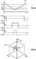
- One possibility of generating a PWM control signal for one of the energy storage modules 3is shown schematically in FIG Fig. 3 illustrated.
- a setpoint signal x Sis compared to a reference signal x R.
- the reference signal x Rcan be a triangular signal which runs between normalized values of -1 and +1.
- the setpoint signal x Scan also have a normalized value between -1 and +1. Shown is a pulse period of duration T during which the pulse width of a PWM control signal for the left branch of the full bridge and thus the switching times of the active switching elements of the left branch of the full bridge are determined by means of a comparison between the setpoint signal x S and the reference signal x R. If the setpoint signal x S is a larger value has as the reference signal x R , the PWM drive signal for the left branch of the full bridge is set to a logic high level.
- the coupling element 7ais placed in an electrically conductive state, while the coupling element 7c is placed in an electrically blocking state.
- the setpoint signal x Shas a smaller value than the reference signal x R , the PWM drive signal for the left branch is set to a logic low level.
- the coupling element 7ais placed in an electrically blocking state, while the coupling element 7c is placed in an electrically conductive state.
- the higher the level of the setpoint signal x Sthe longer the pulse width of the PWM control signal for the left branch during a pulse period T.
- the reference signal x Rrepeats after a pulse period T.
- the pulse width of a PWM control signal for the right branch of the full bridge and thus the switching times of the active switching elements of the right branch of the full bridgeare determined via a comparison between the setpoint signal x S and the reference signal -x R. If the setpoint signal x S has a larger value than the reference signal -x R , the PWM drive signal for the right branch of the full bridge is set to a logic low level. As a result, the coupling element 7d is placed in an electrically conductive state, while the coupling element 7b is placed in an electrically blocking state. If the setpoint signal x S has a smaller value than the reference signal -x R , the PWM drive signal for the right branch is set to a logic high level.
- the coupling element 7dis placed in an electrically blocking state, while the coupling element 7b is placed in an electrically conductive state.
- the higher the level of the setpoint signal x Sthe shorter the pulse width of the PWM control signal for the right branch during a pulse period T.
- the switching times for the active switching elements of the coupling elements 7a to 7d of the coupling device 7can be calculated directly from the without the constant calculation of the instantaneous values of the reference signals x R and -x R
- Setpoint signal x Sis determined by directly calculating only the times at which x S equals x R and when x S equals -x R when using the method described above, relative to the start of the pulse period T of the coupling device 7. These times are the switching times for the coupling elements 7a to 7d.
- a constant value of x Sequal to +2/3.
- the switching stateis first that the coupling elements 7b and 7d are electrically conductive while lock the coupling elements 7a and 7c.
- x Sis then x R , where x R decreases continuously in this first half of the pulse period T. Consequently, the drive signal for the left branch of the full bridge must be switched from the logic low to the logic high level at this time.
- the coupling element 7bis blocked at this time and the coupling element 7a is brought into the electrically conductive state.
- it follows that the coupling element 7dis blocked at the time 5T / 12 and the coupling element 7c is brought into the conductive state.
- the output voltagehas a profile u P which fluctuates between a logically high voltage value and a logically low voltage value, the logically low voltage value being smaller by U M than the logically high voltage value. If x s is positive, the logically high voltage value is + U M , if x s is negative, the logically high voltage value is 0.
- the output voltage u Palternates twice between the logically high and the logically in the course of a pulse period T. low voltage value back and forth.
- the period of the output voltage u Pis equal to T / 2 and thus already halved compared to the period T of the reference signals x R and -x R.
- This control strategycan - as in Fig. 5 illustrated by way of example - expand to a large number of energy storage modules 3 per energy supply branch.
- a setpoint signal x Sis defined for the power supply branch, which scales with the target output voltage of the power supply branch.
- a separate reference signal x Ris generated for each of the energy storage modules 3, each of which has a phase shift with respect to the adjacent reference signals x R of the respective energy supply branch.
- k4 energy storage modules 3 per energy supply branch is shown by way of example, the control strategy also being able to be generalized to other values for k.
- the reference signals x R of the k energy storage modules 3are each shifted by T / 2k against each other.
- the assignment of the respective reference signal pairs x R and -x R to the k energy storage modules 3can be permuted as desired.
- pulse-width-modulated control signalsare now generated for the respective energy storage modules 3 of a power supply branch by comparing the setpoint signal x S with the respectively associated reference signals x R and -x R , this results in a staggering of individual control signals that generate a voltage profile u at the output of the energy supply branch which in Fig. 6 is shown schematically.
- the system of reference signals x Rthus requires an output voltage at the output of the energy supply branch, the range of which is equal to the output voltage U M of an energy storage cell module 5.
- the output voltagefluctuates between a higher and a lower voltage value that is lower by U M , these voltage values both being integer multiples of U M and the average output voltage U resulting in x S ⁇ k ⁇ U M.
- the staggering of the reference signals x Rresults in a period of T / 2k for the period of the alternating component of the output voltage curve. If the output voltage of the energy supply branch were generated instead by a branch of a conventional pulse-controlled inverter, then this branch would have to be supplied with an input voltage of 2 kU M with the same output voltage setting range. The fluctuation range of its output voltage during a pulse period of duration T is then 2 k ⁇ U M , the period of the alternating component of this output voltage is T.
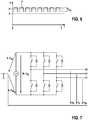
- Fig. 7shows a schematic representation of a conventional pulse-controlled inverter with the input voltage 2 k ⁇ U M , the negative input terminal having the potential -kU M compared to a potential 0 and the positive input terminal having the potential + kU M.
- the switching operations to be carried out in each case during the next sub-pulse period of the duration T / 2kcan also be determined here by type and point in time without the time profiles of the reference signals x R being permanently included must be calculated. To do this, it is only necessary to know the time course of the setpoint signal x S during the next partial pulse period of duration T / 2k. This time course is preferably constant during a partial pulse period of the duration T / 2k. If the setpoint signal x S changes at the beginning of a new sub-pulse period of duration T / 2k, additional switching operations can be triggered at this time. The type of these switching processes can also be determined without explicit constant calculation of the reference signals x R if the value of the setpoint signal x S is known in the preceding and in the newly beginning partial pulse period.
- Fig. 8shows a schematic representation of a control strategy for three different energy supply branches of a pulse inverter supplied with the input voltage 2 k ⁇ U M in accordance with Fig. 7 ,
- the number of threeis exemplary in nature, and it is also possible to have a different number of power supply branches with that in FIG Fig. 8 control strategy shown.
- each of the energy supply branchescan be operated with a different setpoint signal.
- a first power supply branchcan be operated with a setpoint signal x SU , a second power supply branch with a setpoint signal x SV , and a third power supply branch with a setpoint signal x SW .
- each energy supply branchconsists of a half-bridge with a center tap
- the comparison of the respective setpoint signal x S with the reference signal -x Ris omitted.
- the resulting combinations of output voltage values u U , u V and u Ware shown in the space vector diagram in Fig. 9 illustrated.
- the output voltages u U , u V and u Wimplement a star voltage system, which can be applied to the stator terminals of the electrical machine 2, for example to supply energy to a three-phase electrical machine 2.
- Voltage space pointersare set at these stator terminals, which are in Fig. 9 are shown schematically.
- the voltage vector diagram in Fig. 9shows different voltage values u xyz for energy supply branches, each with an energy storage module 3, where the indices x, y and z can assume the value 0 or 1, depending on whether the respective Power supply branch is currently being driven with a PWM control signal with a logic high level or with a PWM control signal with a logic low level.
- three setpoint signals x SU , x SV and x SWare used for the different energy supply branches, which are compared with a staggered phase system of reference signals x R per energy storage module in order to generate the PWM control signals.
- the voltage profiles at the outputs of the energy supply branchesare shown schematically in Fig. 11 illustrated.
- a voltage profile u Uresults on a first energy supply branch
- a voltage profile u Wresults on a third energy supply branch.
- u + 2-i + 2 and u + 2-1-3 2uses the voltage space vector u + 3-1 + 3 and u + 20-2 , which are significantly further away from the setpoint voltage space vector u S than the actually preferred voltage space vector u + 2-1 + 2 . This also increases the voltage fluctuations in the output voltages of the energy supply branches.
- Fig. 1represented schematically, in certain time periods during a partial pulse period T / 2k the output voltages of the three energy supply branches are switched back and forth between two different values. Depending on the respective setpoint signal, it may happen that at the beginning of the partial pulse period T / 2k there is initially the higher of the two output voltages used, which is reduced to the lower of the output voltages in the course of the first half of the partial pulse period, and then in the course the second half of the partial pulse period T / 2k to be raised again to the higher of the two output voltages used.
- the phase offsets of the respective reference signal systems of the various energy supply branchescan be adapted for the less favorable of the two cases.
- the reference signal system of the corresponding power supply branchcan be left unchanged. If, however, the first switching operation took place from low to high output voltage, the reference signal system of the reference signals x R of the corresponding power supply branch can be shifted by a time offset of T / 4k compared to the reference signal systems of the other power supply branches which have been left unchanged. In other words, the reference signals x R of the corresponding power supply branch are shifted by T / 4k in the negative or positive direction on the time axis. As a result, a time interval of duration T / 4k is either skipped or repeated once.
- the reference signal system of the reference signals x R of the corresponding energy supply branchcan be shifted by T / 4k compared to the unchanged reference signal systems of the other energy supply branches if the first switching operation from high to low output voltage would take place. In this case, the first switching process then takes place uniformly in all energy supply branches from low to high output voltage.
- the direction of the time shift by T / 4k along the time axiscan also be selected differently, which only results in other switching operations at the time of the shift of the reference signal system, but the use of the voltage space pointers closest to the setpoint voltage space vector u S is retained.
- any shift in phase of T / 4k + i * T / 2kis possible for the shift of the reference signal system, where i is an integer value.
- Fig. 13shows a schematic representation of a method 10 for controlling an energy storage device, for example the energy storage device 1 in FIG Fig. 1 ,
- the method 10can, for example, by the control device 9 in Fig. 1 be implemented.
- the method 10can have a determination for each of the energy supply branches as to whether the pulse-width-modulated control signal of the energy supply branch is at a logic high or a logic low potential at the beginning of a partial pulse period.
- a selectioncan then be made in a step 12 of those energy supply branches for which the respective pulse-width-modulated control signal of the energy supply branch is at a logic low potential at the beginning of a partial pulse period.
- These energy supply branchescan be referred to as second energy supply branches, the non-selected energy supply branches as first energy supply branches.
- a first pulse-width-modulated control signalis generated for controlling the coupling devices of the respective energy storage modules by comparing a first setpoint signal with a number of 2k first periodic reference signals having a pulse period T, each of which have a phase shift of T / 2k with respect to adjacent first reference signals.
- a second pulse-width-modulated control signalis generated for controlling the coupling devices of the respective energy storage modules by comparing a second setpoint signal with a number of 2k second periodic reference signals having the pulse period T, which each have a phase shift of T / 2k with respect to adjacent second reference signals.
- the second reference signalseach have a phase offset of T / 4k compared to the first reference signals.
- the methodcan also be adapted in a simple manner to battery converter arrangements in which the coupling devices 7 are not designed as full bridges, but only as half bridges.
- the coupling elements 7b and 7d and the output terminal 3bare now connected to either the minus or the positive pole of the energy storage cell module 5 instead of the central tap of the right branch of the full bridge, which is now no longer required. Since the switching operations for the right branch of the full bridge are of course no longer required, all k reference signals are now -x R. The remaining k reference signals x R are then no longer offset by T / 2k but only by T / k compared to the respectively adjacent reference signals. In this case, the duration of a partial pulse period doubles to T / k. Accordingly, the shift between a first system of reference signals and a second system of reference signals then takes place by T / 2k.
Landscapes
- Engineering & Computer Science (AREA)
- Power Engineering (AREA)
- Life Sciences & Earth Sciences (AREA)
- Sustainable Development (AREA)
- Sustainable Energy (AREA)
- Transportation (AREA)
- Mechanical Engineering (AREA)
- Inverter Devices (AREA)
- Charge And Discharge Circuits For Batteries Or The Like (AREA)
Description
Translated fromGermanDie Erfindung betrifft ein System und ein Verfahren zum Ansteuern einer Energiespeichereinrichtung, insbesondere in einer Batteriedirektumrichterschaltung zur Erzeugung einer n-phasigen Wechselspannung.The invention relates to a system and a method for controlling an energy storage device, in particular in a battery direct converter circuit for generating an n-phase AC voltage.
Es zeichnet sich ab, dass in Zukunft sowohl bei stationären Anwendungen, wie z.B. Windkraftanlagen oder Solaranlagen, wie auch in Fahrzeugen, wie Hybrid- oder Elektrofahrzeugen, vermehrt elektronische Systeme zum Einsatz kommen, die neue Energiespeichertechnologien mit elektrischer Antriebstechnik kombinieren.It is becoming apparent that in the future both in stationary applications such as Wind power plants or solar plants, as well as in vehicles such as hybrid or electric vehicles, electronic systems are increasingly being used, which combine new energy storage technologies with electrical drive technology.
Die Einspeisung von mehrphasigem Strom in eine elektrische Maschine wird üblicherweise durch einen Umrichter in Form eines Pulswechselrichters bewerkstelligt. Dazu kann eine von einem Gleichspannungszwischenkreis bereitgestellte Gleichspannung in eine mehrphasige Wechselspannung, beispielsweise eine dreiphasige Wechselspannung umgerichtet werden. Der Gleichspannungszwischenkreis wird dabei von einem Strang aus seriell verschalteten Batteriemodulen gespeist. Um die für eine jeweilige Anwendung gegebenen Anforderungen an Leistung und Energie erfüllen zu können, werden häufig mehrere Batteriemodule in einer Traktionsbatterie in Serie geschaltet.The feeding of multiphase current into an electrical machine is usually accomplished by a converter in the form of a pulse-controlled inverter. For this purpose, a DC voltage provided by a DC voltage intermediate circuit can be converted into a multi-phase AC voltage, for example a three-phase AC voltage. The DC voltage intermediate circuit is fed by a string of battery modules connected in series. In order to be able to meet the performance and energy requirements for a particular application, several battery modules are often connected in series in a traction battery.
In der Druckschrift
BDIs weisen üblicherweise einen höheren Wirkungsgrad und eine höhere Ausfallsicherheit gegenüber herkömmlichen Systemen auf. Die Ausfallsicherheit wird unter anderem dadurch gewährleistet, dass defekte, ausgefallene oder nicht voll leistungsfähige Batteriezellen durch geeignete Überbrückungsansteuerung der Koppeleinheiten aus den Energieversorgungssträngen herausgeschaltet werden können. Die Phasenausgangsspannung eines Energiespeichermodulstrangs kann durch entsprechendes Ansteuern der Koppeleinheiten variiert und insbesondere stufig eingestellt werden. Die Stufung der Ausgangsspannung ergibt sich dabei aus der Spannung eines einzelnen Energiespeichermoduls, wobei die maximal mögliche Phasenausgangsspannung die Summe der Spannungen aller Energiespeichermodule eines Energiespeichermodulstrangs bestimmt wird.BDIs are usually more efficient and more reliable than conventional systems. The reliability is guaranteed, among other things, by the fact that defective, failed or not fully efficient battery cells can be switched out of the energy supply lines by suitable bridging control of the coupling units. The phase output voltage of an energy storage module string can be varied by appropriate activation of the coupling units and in particular can be set in stages. The gradation of the output voltage results from the voltage of an individual energy storage module, the maximum possible phase output voltage determining the sum of the voltages of all energy storage modules of an energy storage module string.
Zur Einstellung einer Ausgangsspannung eines Energiespeichermoduls kann eine pulsbreitenmodulierte (PWM) Ansteuerung der Koppeleinheiten erfolgen. Dadurch ist es möglich, durch gezielte Variation der Ein- bzw. Ausschaltzeiten einen gewünschten Mittelwert als Energiespeichermodulspannung auszugeben.A pulse width modulated (PWM) control of the coupling units can be carried out to set an output voltage of an energy storage module. This makes it possible to output a desired mean value as an energy storage module voltage by specifically varying the switch-on and switch-off times.
Aus der Druckschrift
Für BDIs besteht ein Bedarf nach PWM-Ansteuerverfahren, bei denen die Schwankung der Gesamt-Ausgangsspannung optimiert werden kann, insbesondere bei einer Erzeugung eines n-phasigen Ausgangsspannungssystems in einem n-phasigen BDI.There is a need for BDIs for PWM control methods in which the fluctuation of the total output voltage can be optimized, in particular when generating an n-phase output voltage system in an n-phase BDI.
Aus der Druckschrift
Die vorliegende Erfindung schafft gemäß einem Aspekt ein Verfahren gemäß Anspruch 1.In one aspect, the present invention provides a method in accordance with claim 1.
Gemäß einem weiteren Aspekt schafft die vorliegende Erfindung ein System gemäß Anspruch 10.In another aspect, the present invention provides a system according to
Es ist Idee der vorliegenden Erfindung, die Ansteuerstrategie einer Energiespeichereinrichtung mit mehreren Phasenanschlüssen zur Erzeugung einer mehrphasigen Versorgungsspannung aus einer Vielzahl von Energiespeichermodulen über ein PWM-Verfahren derart zu optimieren, dass stets nur diejenigen Spannungsraumzeiger im System der über ein PWM-Ansteuersignal angesteuerten Energiespeichermodule verwendet werden, welche sich dem Soll-Spannungsraumzeiger am nächsten befinden. Dazu werden PWM-Ansteuersignale für verschiedene Energieversorgungszweige so erzeugt, dass die für die Erzeugung herangezogenen Referenzsignale von Energieversorgungszweig zu Energieversorgungszweig verschiedene Phasenversätze zueinander aufweisen. Wenn der Phasenversatz einen Bruchteil des Phasenversatzes, den die Referenzsignale innerhalb eines Energieversorgungszweigs untereinander aufweisen, beträgt, erfolgt die Auswahl der Spannungsraumzeiger automatisch dergestalt, dass nur die dem Soll-Spannungsraumzeiger unmittelbar benachbarten Spannungsraumzeiger zur Erzeugung der Phasenspannungen herangezogen werden.It is the idea of the present invention to optimize the control strategy of an energy storage device with a plurality of phase connections for generating a multi-phase supply voltage from a multiplicity of energy storage modules by means of a PWM method such that only those voltage space pointers are used in the system of the energy storage modules controlled by a PWM control signal which are closest to the target voltage space pointer. For this purpose, PWM control signals for different energy supply branches are generated in such a way that the reference signals used for the generation have different phase offsets from one energy supply branch to the other. If the phase offset is a fraction of the phase offset that the reference signals have within one power supply branch, the voltage space pointers are automatically selected such that only the voltage space pointers directly adjacent to the target voltage space pointer are used to generate the phase voltages.
Ein erheblicher Vorteil dieser Vorgehensweise besteht darin, dass sich die Stromschwankungen in der Energiespeichereinrichtung und im angeschlossenen Verbraucher reduzieren lassen, was die Belastung der Schaltelemente der Energiespeichereinrichtung verringert. Umgekehrt kann die Schaltfrequenz der Koppeleinrichtungen der Energiespeichereinrichtung bei gleichbleibender Höhe der Stromschwankungen in der Energiespeichereinrichtung reduziert werden.A significant advantage of this procedure is that the current fluctuations in the energy storage device and in the connected one Let consumers reduce, which reduces the load on the switching elements of the energy storage device. Conversely, the switching frequency of the coupling devices of the energy storage device can be reduced while the current fluctuations in the energy storage device remain constant.
Gemäß dem erfindungsgemäßen Verfahren erfolgt weiterhin für jeden der Energieversorgungszweige ein Bestimmen, ob sich das pulsbreitenmodulierte Ansteuersignal des Energieversorgungszweigs zu Beginn einer Teilpulsperiode auf einem logisch hohen oder einem logisch niedrigen Potential befindet.According to the method according to the invention, a determination is also made for each of the energy supply branches whether the pulse-width-modulated control signal of the energy supply branch is at a logically high or a logically low potential at the beginning of a partial pulse period.
Vorteilhafterweise kann dann in einer weiteren Ausführungsform ein Auswählen derjenigen Energieversorgungszweige, für die sich das jeweilige pulsbreitenmodulierte Ansteuersignal des Energieversorgungszweigs zu Beginn einer Teilpulsperiode auf einem logisch niedrigen Potential befindet, als zweite Energieversorgungszweige erfolgen. Dadurch kann zu Beginn jeder Pulsperiode überprüft werden, welche Ansteuerstrategie für die Koppeleinrichtungen der Energiespeichermodule mit den geringsten Stromschwankungen verbunden ist.In a further embodiment, the energy supply branches for which the respective pulse-width-modulated control signal of the energy supply branch is at a logic low potential at the beginning of a partial pulse period can then advantageously be selected as second energy supply branches. This makes it possible to check at the beginning of each pulse period which control strategy for the coupling devices of the energy storage modules is associated with the smallest current fluctuations.
Gemäß einer weiteren Ausführungsform des erfindungsgemäßen Verfahrens kann der Phasenversatz der zweiten Referenzsignale gegenüber den ersten Referenzsignalen positiv sein. Alternativ dazu kann gemäß einer weiteren Ausführungsform des erfindungsgemäßen Verfahrens der Phasenversatz der zweiten Referenzsignale gegenüber den ersten Referenzsignalen negativ sein. Dadurch kann die Abfolge der Schaltvorgänge vorteilhafterweise an die Ansteuerstrategie angepasst werden.According to a further embodiment of the method according to the invention, the phase offset of the second reference signals can be positive compared to the first reference signals. Alternatively, according to a further embodiment of the method according to the invention, the phase offset of the second reference signals can be negative with respect to the first reference signals. As a result, the sequence of switching operations can advantageously be adapted to the control strategy.
Gemäß einer weiteren Ausführungsform des erfindungsgemäßen Verfahrens können die ersten und zweiten Referenzsignale Dreiecksignale sein.According to a further embodiment of the method according to the invention, the first and second reference signals can be triangular signals.
Gemäß einer weiteren Ausführungsform des erfindungsgemäßen Verfahrens können die ersten und zweiten Sollwertsignale zumindest über eine Pulsperiode hinweg konstanten Signalpegel aufweisen.According to a further embodiment of the method according to the invention, the first and second setpoint signals can have constant signal levels at least over a pulse period.
Gemäß einer Ausführungsform des erfindungsgemäßen Systems können die Koppeleinrichtungen Leistungs-MOSFET-Schalter oder IGBT-Schalter aufweisen.According to one embodiment of the system according to the invention, the coupling devices can have power MOSFET switches or IGBT switches.
Weitere Merkmale und Vorteile von Ausführungsformen der Erfindung ergeben sich aus der nachfolgenden Beschreibung mit Bezug auf die beigefügten Zeichnungen.Further features and advantages of embodiments of the invention will become apparent from the following description with reference to the accompanying drawings.
Es zeigen:
- Fig. 1
- eine schematische Darstellung eines Systems mit einer Energiespeichereinrichtung gemäß einer Ausführungsform der vorliegenden Erfindung;
- Fig. 2
- eine schematische Darstellung eines Energiespeichermoduls einer Energiespeichereinrichtung nach
Fig. 1 ; - Fig. 3
- eine schematische Darstellung einer PWM-Ansteuerstrategie eines Energiespeichermoduls einer Energiespeichereinrichtung;
- Fig. 4
- eine schematische Darstellung eines Potentialdiagramms der Ausgangsspannung eines Energiespeichermoduls einer Energiespeichereinrichtung, welches mit einer PWM-Ansteuerstrategie gemäß
Fig. 4 betrieben wird; - Fig. 5
- eine schematische Darstellung einer PWM-Ansteuerstrategie einer Energiespeichereinrichtung mit einer Vielzahl von Energiespeichermodulen;
- Fig. 6
- eine schematische Darstellung eines Potentialdiagramms der Ausgangsspannung einer Energiespeichereinrichtung mit einer Vielzahl von Energiespeichermodulen, welches mit einer PWM-Ansteuerstrategie gemäß
Fig. 5 betrieben wird; - Fig. 7
- eine schematische Darstellung eines Pulswechselrichters;
- Fig. 8
- eine schematische Darstellung einer PWM-Ansteuerstrategie einer Energiespeichereinrichtung mit einer Vielzahl von Energieversorgungszweigen;
- Fig. 9
- eine schematische Darstellung eines Spannungsraumzeigerdiagramms einer Energiespeichereinrichtung mit einer Vielzahl von Energieversorgungszweigen, welche mit einer PWM-Ansteuerstrategie gemäß
Fig. 8 betrieben wird; - Fig. 10
- eine schematische Darstellung einer Ansteuerstrategie einer Energiespeichereinrichtung mit einer Vielzahl von Energieversorgungszweigen, welche jeweils eine Vielzahl von Energiespeichermodulen aufweisen;
- Fig. 11
- eine schematische Darstellung eines Potentialdiagramms der Ausgangsspannung einer Energiespeichereinrichtung mit einer Vielzahl von Energieversorgungszweigen, welche jeweils eine Vielzahl von Energiespeichermodulen aufweisen, wobei die Energiespeichereinrichtung mit einer PWM-Ansteuerstrategie gemäß
Fig. 10 betrieben wird; - Fig. 12
- eine schematische Darstellung eines Spannungsraumzeigerdiagramms einer Energiespeichereinrichtung mit einer Vielzahl von Energieversorgungszweigen, welche jeweils eine Vielzahl von Energiespeichermodulen aufweisen, wobei die Energiespeichereinrichtung mit einer PWM-Ansteuerstrategie gemäß
Fig. 10 betrieben wird; und - Fig. 13
- eine schematische Darstellung eines Verfahrens zum Ansteuern einer Energiespeichereinrichtung gemäß einer Ausführungsform der vorliegenden Erfindung.
- Fig. 1
- a schematic representation of a system with an energy storage device according to an embodiment of the present invention;
- Fig. 2
- is a schematic representation of an energy storage module of an energy storage device according to
Fig. 1 ; - Fig. 3
- a schematic representation of a PWM control strategy of an energy storage module of an energy storage device;
- Fig. 4
- a schematic representation of a potential diagram of the output voltage of an energy storage module of an energy storage device, which according to a PWM control strategy
Fig. 4 is operated; - Fig. 5
- a schematic representation of a PWM control strategy of an energy storage device with a plurality of energy storage modules;
- Fig. 6
- a schematic representation of a potential diagram of the output voltage of an energy storage device with a plurality of energy storage modules, which according to a PWM control strategy
Fig. 5 is operated; - Fig. 7
- a schematic representation of a pulse inverter;
- Fig. 8
- a schematic representation of a PWM control strategy of an energy storage device with a plurality of energy supply branches;
- Fig. 9
- a schematic representation of a voltage space vector diagram of an energy storage device with a plurality of energy supply branches, which according to a PWM control strategy
Fig. 8 is operated; - Fig. 10
- a schematic representation of a control strategy of an energy storage device with a plurality of energy supply branches, each having a plurality of energy storage modules;
- Fig. 11
- is a schematic representation of a potential diagram of the output voltage of an energy storage device with a plurality of energy supply branches, each having a plurality of energy storage modules, the energy storage device with a PWM control strategy according to
Fig. 10 is operated; - Fig. 12
- a schematic representation of a voltage space vector diagram of an energy storage device with a plurality of energy supply branches, each having a plurality of energy storage modules, the energy storage device with a PWM control strategy according to
Fig. 10 is operated; and - Fig. 13
- is a schematic representation of a method for controlling an energy storage device according to an embodiment of the present invention.
Das System 100 kann weiterhin eine Steuereinrichtung 9 umfassen, welche mit der Energiespeichereinrichtung 1 verbunden ist, und mithilfe derer die Energiespeichereinrichtung 1 gesteuert werden kann, um die gewünschten Ausgangsspannungen an den jeweiligen ersten Ausgangsanschlüssen 1a, 1b, 1c bereitzustellen. Zudem kann die Steuereinrichtung 9 dazu ausgelegt sein, bei einem Laden der Energiespeicherzellen der Energiespeichereinrichtung 1 die jeweiligen aktiven Schaltelemente der Energiespeichereinrichtung 1 anzusteuern.The
Die Energieversorgungszweige können mit jeweils einem Ende an einem gemeinsamen Sternpunkt 4 zusammengeführt sein. Das Potenzial dieses Sternpunkts 4 kann per Definition als das Potenzial 0 gewählt sein. Der Sternpunkt 4 kann auch mit dem Massepotenzial des Fahrzeugs elektrisch leitend verbunden sein.The energy supply branches can each be brought together at one end at a
Jeder der Energieversorgungszweige weist mindestens zwei in Reihe geschaltete Energiespeichermodule 3 auf. Beispielhaft beträgt die Anzahl der Energiespeichermodule 3 pro Energieversorgungszweig in
Die Energiespeichermodule 3 weisen jeweils zwei Ausgangsanschlüsse 3a und 3b auf, über welche eine Ausgangsspannung der Energiespeichermodule 3 bereitgestellt werden kann. Da die Energiespeichermodule 3 primär in Reihe geschaltet sind, summieren sich die Ausgangsspannungen der Energiespeichermodule 3 zu einer Gesamt-Ausgangsspannung, welche an dem jeweiligen der ersten Ausgangsanschlüsse 1a, 1b, 1c der Energiespeichereinrichtung 1 bereitgestellt werden kann.The
Eine beispielhafte Aufbauform der Energiespeichermodule 3 ist in
Das Energiespeicherzellenmodul 5 kann dabei beispielsweise in Reihe geschaltete Zellen 5a bis 5i, beispielsweise Lithium-Ionen-Zellen aufweisen. Dabei beträgt die Anzahl der Energiespeicherzellen 5a bis 5i in den in
Die Energiespeicherzellenmodule 5 weisen eine Klemmenspannung von UM auf und sind über Verbindungsleitungen mit Eingangsanschlüssen der zugehörigen Koppeleinrichtung 7 verbunden. An den Eingangsklemmen der zugehörigen Koppeleinrichtung 7 liegt also die Spannung UM an. Dabei bilden die in Reihe geschalteten Koppelelemente 7a und 7c, deren Mittelabgriff mit der Ausgangsklemmen 3a verbunden ist, den so genannten linken Zweig der Vollbrücke und es bilden die in Reihe geschalteten Koppelelemente 7b und 7d, deren Mittelabgriff mit der Ausgangsklemme 3b verbunden ist, den so genannten rechten Zweig der Vollbrücke. Die Koppeleinrichtung 7 ist in
Die Koppelelemente 7a, 7b, 7c, 7d können derart angesteuert werden, beispielsweise mit Hilfe der in
Durch geeignetes Ansteuern der Koppeleinrichtungen 7 können daher einzelne Energiespeicherzellenmodule 5 der Energiespeichermodule 3 gezielt in die Reihenschaltung eines Energieversorgungszweigs integriert werden. Dadurch kann durch eine gezielte Ansteuerung der Koppeleinrichtungen 7 zum selektiven Schalten der Energiespeicherzellenmodule 5 der Energiespeichermodule 3 in die Energieversorgungszweige eine Gesamt-Ausgangsspannung an jedem der Ausgangsanschlüsse 1a, 1b, 1c bereitgestellt werden, die von den einzelnen Ausgangsspannungen der Energiespeicherzellenmodule 5 der Energiespeichermodule 3 abhängig ist. Die Gesamt-Ausgangsspannung kann dabei jeweils in Stufen eingestellt werden, wobei die Anzahl der Stufen mit der Anzahl der Energiespeichermodule 3 pro Energieversorgungszweig skaliert. Bei einer Anzahl von k Energiespeichermodulen 3 in einem Energieversorgungszweig kann die Gesamt-Ausgangsspannung der Energieversorgungszweigs in 2k+1 Stufen zwischen -k·UM,...,0,...,+k·UM eingestellt werden.By suitably actuating the
Über eine pulsbreitenmodulierte (PWM)-Ansteuerung kann an jedem der Ausgangsanschlüsse 1a, 1b, 1c eine Folge von Ausgangsspannungen eingestellt werden, deren Spannungsverlauf sich dem einer sinusförmigen Wechselspannung annähert. Dazu kann den Koppelelementen 7a, 7c bzw. 7b, 7d jeder Halbbrücke der Energiespeichermodule 3 über geeignete Variation der Pulsbreiten eines PWM-Ansteuersignals ein gewünschter Ablauf von Schaltvorgängen vorgegeben werden. Eine Möglichkeit, ein PWM-Ansteuersignal für eines der Energiespeichermodule 3 zu erzeugen, ist schematisch in
Ein Sollwertsignal xS wird dazu mit einem Referenzsignal xR verglichen. Das Referenzsignal xR kann dabei ein Dreiecksignal sein, welches zwischen normierten Werten von -1 und +1 verläuft. Das Sollwertsignal xS kann dabei ebenfalls einen normierten Wert zwischen -1 und +1 aufweisen. Gezeigt ist eine Pulsperiode der Dauer T, während der die Pulsbreite eines PWM-Ansteuersignals für den linken Zweig der Vollbrücke und damit die Schaltzeitpunkte der aktiven Schaltelemente des linken Zweigs der Vollbrücke über einen Vergleich zwischen dem Sollwertsignal xS und dem Referenzsignal xR bestimmt werden. Wenn das Sollwertsignal xS einen größeren Wert aufweist als das Referenzsignal xR, wird das PWM-Ansteuersignal für den linken Zweig der Vollbrücke auf einen logisch hohen Pegel gesetzt. Dies hat zur Folge, dass das Koppelelement 7a in einen elektrisch leitenden Zustand versetzt wird, während das Koppelelement 7c in einen elektrisch sperrenden Zustand versetzt wird. Wenn das Sollwertsignal xS einen kleineren Wert aufweist als das Referenzsignal xR, wird das PWM-Ansteuersignal für den linken Zweig auf einen logisch niedrigen Pegel gesetzt. Dies hat zur Folge, dass das Koppelelement 7a in einen elektrisch sperrenden Zustand versetzt wird, während das Koppelelement 7c in einen elektrisch leitenden Zustand versetzt wird. Je höher der Pegel des Sollwertsignals xS dabei ist, desto länger ist die Pulsbreite des PWM-Ansteuersignals für den linken Zweig während einer Pulsperiode T. Das Referenzsignal xR wiederholt sich nach einer Pulsperiode T.A setpoint signal xS is compared to a reference signal xR. The reference signal xR can be a triangular signal which runs between normalized values of -1 and +1. The setpoint signal xS can also have a normalized value between -1 and +1. Shown is a pulse period of duration T during which the pulse width of a PWM control signal for the left branch of the full bridge and thus the switching times of the active switching elements of the left branch of the full bridge are determined by means of a comparison between the setpoint signal xS and the reference signal xR. If the setpoint signal xS is a larger value has as the reference signal xR , the PWM drive signal for the left branch of the full bridge is set to a logic high level. As a result, the
In entsprechender Weise werden die Pulsbreite eines PWM-Ansteuersignals für den rechten Zweig der Vollbrücke und damit die Schaltzeitpunkte der aktiven Schaltelemente des rechten Zweigs der Vollbrücke über einen Vergleich zwischen dem Sollwertsignal xS und dem Referenzsignal -xR bestimmt. Wenn das Sollwertsignal xS einen größeren Wert aufweist als das Referenzsignal -xR, wird das PWM-Ansteuersignal für den rechten Zweig der Vollbrücke auf einen logisch niedrigen Pegel gesetzt. Dies hat zur Folge, dass das Koppelelement 7d in einen elektrisch leitenden Zustand versetzt wird, während das Koppelelement 7b in einen elektrisch sperrenden Zustand versetzt wird. Wenn das Sollwertsignal xS einen kleineren Wert aufweist als das Referenzsignal -xR, wird das PWM-Ansteuersignal für den rechten Zweig auf einen logisch hohen Pegel gesetzt. Dies hat zur Folge, dass das Koppelelement 7d in einen elektrisch sperrenden Zustand versetzt wird, während das Koppelelement 7b in einen elektrisch leitenden Zustand versetzt wird. Je höher der Pegel des Sollwertsignals xS dabei ist, desto kürzer ist die Pulsbreite des PWM-Ansteuersignals für den rechten Zweig während einer Pulsperiode T.In a corresponding manner, the pulse width of a PWM control signal for the right branch of the full bridge and thus the switching times of the active switching elements of the right branch of the full bridge are determined via a comparison between the setpoint signal xS and the reference signal -xR. If the setpoint signal xS has a larger value than the reference signal -xR , the PWM drive signal for the right branch of the full bridge is set to a logic low level. As a result, the
Ist das Sollwertsignal xS während einer Pulsperiode konstant oder ist zumindest dessen zeitlicher Verlauf bekannt, so können die Schaltzeitpunkte für die aktiven Schaltelemente der Koppelelemente 7a bis 7d der Koppeleinrichtung 7 auch ohne ständige Berechnung der Momentanwerte der Referenzsignale xR und -xR direkt aus dem Sollwertsignal xS bestimmt werden, indem nur die Zeitpunkte, zu denen bei Anwendung des oben beschriebenen Verfahrens xS gleich xR und zu denen xS gleich -xR ist, relativ zum Beginn der Pulsperiode T der Koppeleinrichtung 7 direkt berechnet werden. Diese Zeitpunkte sind die Schaltzeitpunkte für die Koppelelemente 7a bis 7d. Zu dem in
Wie in
Diese Ansteuerstrategie lässt sich - wie in
Dadurch entsteht ein System von 2k Referenzsignalen xR1 bis xRk und -xR1 bis -xRk. Die Zuordnung der jeweiligen Referenzsignalpaare xR und -xR zu den k Energiespeichermodulen 3 kann dabei beliebig permutiert sein.This creates a system of 2k reference signals xR1 to xRk and -xR1 to -xRk . The assignment of the respective reference signal pairs xR and -xR to the k
Erzeugt man nun für die jeweiligen Energiespeichermodule 3 eines Energieversorgungszweigs pulsbreitenmodulierte Ansteuersignale über einen Vergleich des Sollwertsignals xS mit den jeweils zugehörigen Referenzsignalen xR und -xR, so ergibt sich eine Staffelung an Einzel-Ansteuersignalen, die einen Spannungsverlauf u am Ausgang des Energieversorgungszweigs erzeugen, welcher in
Die Stromschwankungen des oben beschriebenen Batteriedirektumrichters in Verbindung mit dem beschriebenen PWM-Verfahren reduzieren sich also gegenüber einem mit gleicher PWM-Periodendauer T betriebenen, herkömmlichen Pulswechselrichter mit gleichem Ausgangsstellbereich um einen Faktor von 1/2k*1/2k = (1/2k)2, so dass sich die Schaltfrequenz gegenüber einer herkömmlichen Ansteuerstrategie senken lässt, ohne dass die Stromschwankungen vorgegebene Schwellwerte überschreiten.The current fluctuations of the above-described direct battery converter in connection with the described PWM method are thus reduced by a factor of 1 / 2k * 1 / 2k = (1 / 2k)2 compared to a conventional pulse-controlled inverter with the same output setting range operated with the same PWM period T , so that the switching frequency can be reduced compared to a conventional control strategy without the current fluctuations exceeding predetermined threshold values.
Wie schon bei der Beschreibung des PWM-Verfahrens für eine Koppeleinrichtung 7 erläutert, lassen sich auch hier die jeweils während der nächsten Teilpulsperiode der Dauer T/2k auszuführenden Schaltvorgänge nach Art und Zeitpunkt bestimmen, ohne dass dazu die zeitlichen Verläufe der Referenzsignale xR permanent mit berechnet werden müssen. Hierzu muss lediglich der zeitliche Verlauf des Sollwertsignals xS während der nächsten Teilpulsperiode der Dauer T/2k bekannt sein. Vorzugsweise ist dieser zeitliche Verlauf während einer Teilpulsperiode der Dauer T/2k konstant. Bei einer Änderung des Sollwertsignals xS zu Beginn einer neuen Teilpulsperiode der Dauer T/2k können zu diesem Zeitpunkt zusätzliche Schaltvorgänge ausgelöst werden. Auch die Art dieser Schaltvorgänge lässt sich ohne explizite ständige Berechnung der Referenzsignale xR bestimmen, wenn der Wert des Sollwertsignals xS in der vorhergehenden und in der neu beginnenden Teilpulsperiode jeweils bekannt ist.As already explained in the description of the PWM method for a
Das Spannungszeigerdiagramm in
Wiederum ist es wünschenswert, den Sollwertspannungsraumzeiger uS mit denjenigen Spannungsraumzeigern darzustellen, welche dem Sollwertspannungsraumzeiger uS am nächsten liegen. Verwendet man nun für die Referenzsignale xR in
Die Ursache dieses Problems liegt darin begründet, dass für einen dreiphasigen BDI, wie in
Im System der Referenzsignale xR lässt sich feststellen, dass der erste Schaltvorgang einer Pulsperiode immer dann von hoher zu niedriger Ausgangsspannung erfolgt, wenn das erste der Referenzsignale, welches das Sollwertsignal xS schneidet, ansteigt, das heißt, einen positiven Gradienten aufweist. Umgekehrt erfolgt der erste Schaltvorgang einer Pulsperiode immer dann von niedriger zu hoher Ausgangsspannung, wenn das erste der Referenzsignale, welches das Sollwertsignal xS schneidet, fällt, das heißt, einen negativen Gradienten aufweist. Wenn also zu Beginn jeder Pulsperiode für jeden der Energieversorgungszweige bestimmt wird, ob der erste Schaltvorgang von hoher zu niedriger Ausgangsspannung oder von niedriger zu hoher Ausgangsspannung erfolgt, kann für den ungünstigeren der beiden Fälle eine Anpassung der Phasenversätze der jeweiligen Referenzsignalsysteme der verschiedenen Energieversorgungszweige erfolgen. Falls der erste Schaltvorgang von hoher zu niedriger Ausgangsspannung erfolgt, so kann das Referenzsignalsystem des entsprechenden Energieversorgungszweigs unverändert belassen werden. Falls der erste Schaltvorgang jedoch von niedriger zu hoher Ausgangsspannung erfolgen würde, so kann das Referenzsignalsystem der Referenzsignale xR des entsprechenden Energieversorgungszweigs gegenüber den unverändert belassenen Referenzsignalsystemen der anderen Energieversorgungszweige um einen Zeitversatz von T/4k verschoben werden. Mit anderen Worten werden die Referenzsignale xR des entsprechenden Energieversorgungszweigs um T/4k in negative oder positive Richtung auf der Zeitachse verschoben. Dadurch wird ein Zeitintervall der Dauer T/4k entweder übersprungen oder ein Mal wiederholt.In the system of reference signals xR, it can be determined that the first switching operation of a pulse period always takes place from high to low output voltage when the first of the reference signals, which intersects the setpoint signal xS , rises, that is to say has a positive gradient. Conversely, the first switching process takes place a pulse period from low to high output voltage whenever the first of the reference signals, which intersects the setpoint signal xS , falls, that is to say has a negative gradient. Thus, if it is determined at the beginning of each pulse period for each of the energy supply branches whether the first switching operation takes place from high to low output voltage or from low to high output voltage, the phase offsets of the respective reference signal systems of the various energy supply branches can be adapted for the less favorable of the two cases. If the first switching process takes place from high to low output voltage, the reference signal system of the corresponding power supply branch can be left unchanged. If, however, the first switching operation took place from low to high output voltage, the reference signal system of the reference signals xR of the corresponding power supply branch can be shifted by a time offset of T / 4k compared to the reference signal systems of the other power supply branches which have been left unchanged. In other words, the reference signals xR of the corresponding power supply branch are shifted by T / 4k in the negative or positive direction on the time axis. As a result, a time interval of duration T / 4k is either skipped or repeated once.
Mit dieser Vorgehensweise kann erreicht werden, dass der erste Schaltvorgang in allen Energieversorgungszweigen einheitlich von hoher zu niedriger Ausgangsspannung erfolgt, so dass nur noch die dem Sollwertspannungsraumzeiger uS am nächsten liegenden Spannungsraumzeiger genutzt werden. Dies bedeutet, dass die Spannungs- bzw. Stromschwankungen in den Ausgangsspannungen der einzelnen Energieversorgungszweige auf ein Minimum werden können.With this procedure it can be achieved that the first switching operation takes place uniformly in all energy supply branches from high to low output voltage, so that only the voltage space pointers closest to the setpoint voltage space vector uS are used. This means that the voltage or current fluctuations in the output voltages of the individual energy supply branches can be kept to a minimum.
Es ist selbstverständlich auch möglich, dass das Referenzsignalsystem der Referenzsignale xR des entsprechenden Energieversorgungszweigs gegenüber den unverändert belassenen Referenzsignalsystemen der anderen Energieversorgungszweige um T/4k verschoben werden kann, falls der erste Schaltvorgang von hoher zu niedriger Ausgangsspannung erfolgen würde. In diesem Fall erfolgt dann der erste Schaltvorgang in allen Energieversorgungszweigen einheitlich von niedriger zu hoher Ausgangsspannung. Die Richtung der zeitlichen Verschiebung um T/4k entlang der Zeitachse kann ebenfalls unterschiedlich gewählt werden, wodurch sich lediglich andere Schaltvorgänge zum Zeitpunkt der Verschiebung des Referenzsignalsystems ergeben, die Nutzung der dem Sollwertspannungsraumzeiger uS am nächsten liegenden Spannungsraumzeiger aber beibehalten wird. Allgemein gesprochen ist für die Verschiebung des Referenzsignalsystems jeder Phasenversatz von T/4k + i * T/2k möglich, wobei i ein ganzzahliger Wert ist.It is of course also possible that the reference signal system of the reference signals xR of the corresponding energy supply branch can be shifted by T / 4k compared to the unchanged reference signal systems of the other energy supply branches if the first switching operation from high to low output voltage would take place. In this case, the first switching process then takes place uniformly in all energy supply branches from low to high output voltage. The direction of the time shift by T / 4k along the time axis can also be selected differently, which only results in other switching operations at the time of the shift of the reference signal system, but the use of the voltage space pointers closest to the setpoint voltage space vector uS is retained. Generally spoken, any shift in phase of T / 4k + i * T / 2k is possible for the shift of the reference signal system, where i is an integer value.
In einem Schritt 13 erfolgt für eine Anzahl k an Energiespeichermodulen mindestens eines ersten Energieversorgungszweigs, ein Erzeugen eines ersten pulsbreitenmodulierten Ansteuersignals zum Ansteuern der Koppeleinrichtungen der jeweiligen Energiespeichermodule durch Vergleichen eines ersten Sollwertsignals mit einer Anzahl von 2k ersten, eine Pulsperiode T aufweisenden periodischen Referenzsignalen, welche jeweils einen Phasenversatz von T/2k gegenüber benachbarten ersten Referenzsignalen aufweisen. Gleichzeitig erfolgt in einem Schritt 13 für eine Anzahl k an Energiespeichermodulen mindestens eines zweiten Energieversorgungszweigs, ein Erzeugen eines zweiten pulsbreitenmodulierten Ansteuersignals zum Ansteuern der Koppeleinrichtungen der jeweiligen Energiespeichermodule durch Vergleichen eines zweiten Sollwertsignals mit einer Anzahl von 2k zweiten, die Pulsperiode T aufweisenden periodischen Referenzsignalen, welche jeweils einen Phasenversatz von T/2k gegenüber benachbarten zweiten Referenzsignalen aufweisen. Dabei weisen die zweiten Referenzsignale gegenüber den ersten Referenzsignalen jeweils einen Phasenversatz von T/4k auf.In a
Mit dieser Vorgehensweise kann sichergestellt werden, dass stets diejenigen Spannungsraumzeiger zur Darstellung eines Sollwertspannungsraumzeigers genutzt werden, die dem Sollwertspannungsraumzeiger am nächsten liegen. Dadurch können die Strom- und Spannungsschwankungen in einer Energiespeichereinrichtung wie in
Wie bereits beschrieben ist es besonders vorteilhaft, die Auswahl, ob das Referenzsignalsystem eines Energieversorgungszweiges auf der Zeitachse verschoben werden soll oder nicht sowie eine daraus sich gegebenenfalls ergebende Verschiebung dieses Referenzsignalsystems um T/4k auf der Zeitachse jeweils zu Beginn jeder Teil-Pulsperiode auszuführen. Ferner ist es vorteilhaft, die Sollwertsignale xS der Energieversorgungszweige jeweils innerhalb einer Teilpulsperiode der Dauer T/2k konstant zu halten.As already described, it is particularly advantageous to carry out the selection as to whether or not the reference signal system of a power supply branch is to be shifted on the time axis, and to shift this reference signal system by T / 4k on the time axis, which may result therefrom, at the beginning of each partial pulse period. Furthermore, it is advantageous to keep the setpoint signals xS of the energy supply branches constant within a partial pulse period of the duration T / 2k.
Das Verfahren kann in einfacher Weise auch auf Batterie-Umrichteranordnungen angepasst werden, bei denen die Koppeleinrichtungen 7 nicht als Vollbrücken, sondern nur als Halbbrücken ausgeführt sind. In diesem Fall entfallen gegenüber der Darstellung in
Claims (11)
- Method (10) for controlling an energy storage device (1) that comprises:
n output connectors (1a, 1b, 1c), wherein n ≥ 2, for the purpose of providing a supply voltage at each of the output connectors (1a, 1b, 1c), and n energy supply branches that are coupled in each case to one of the output connectors (1a, 1b, 1c), wherein each of the energy supply branches comprises several series-connected energy storage modules (3) that in each case comprise:an energy storage cell module (5) that comprises at least one energy storage cell (5a, 5k), anda coupling device (7) having coupling elements (7a, 7b, 7c, 7d) in a full bridge circuit, which coupling elements are designed so as to selectively connect the energy storage cell module (5) into the respective energy supply branch or bridge said energy storage cell module,wherein the method (10) comprises the steps:of generating (13) a first pulse width modulated control signal for a number k of energy storage modules (3) at least of one first energy supply branch for the purpose of controlling the coupling devices (7) of the respective energy storage modules (3) by means of comparing a first desired value signal (xSU) with a number of 2k first periodic reference signals (xR) that comprise a pulse period T, which periodic reference signals that in each case comprise a phase shift of T/2k with respect to adjacent first reference signals (xR); andof generating (14) a second pulse width modulated control signal for a number k of energy storage modules (3) one at least of second energy supply branch for the purpose of controlling the coupling devices (7) of the respective energy storage modules (3) by means of comparing a second desired value signal (xSV; xSW) with a number of 2k second periodic reference signals (xR) that comprise the pulse period T, which periodic reference signals in each case comprise a phase shift of T/2k with respect to adjacent second reference signals (xR),characterized by determining for each of the energy supply branches whether the pulse width modulated control signal of the energy supply branch is at a logic "high" potential or a logic "low" potential at the beginning of a partial pulse period of the duration T/2k and based on said determining, displacing a reference signal system of second reference signals (xR) of an energy supply branch by a phase shift of T/4k with respect to a reference signal system of first reference signals (xR) of an energy supply branch which remains unchanged, such that the first switching process in the energy supply branches occurs in a uniform manner from the high output voltage to the low output voltage or in a uniform manner from the low output voltage to the high output voltage. - Method (10) according to Claim 1, furthermore with the step:
of selecting (12) as second energy supply branches those energy supply branches for which the respective pulse width modulated control signal of the energy supply branch is at a logic "low" potential at the beginning of a partial pulse period (T/2k). - Method (10) according to Claim 1, furthermore with the step:
of selecting (12) as second energy supply branches the energy supply branches for which the respective pulse width modulated control signal of the energy supply branch is at a logic "high" potential at the beginning of a partial pulse period (T/2k). - Method (10) according to any one of Claims 1 to 3, wherein the phase shift of the second reference signals is positive with respect to the first reference signals.
- Method (10) according to any one of Claims 1 to 3, wherein the phase shift of the second reference signals is negative with respect to the first reference signals.
- Method (10) according to any one of Claims 1 to 5, wherein a change from the reference signal system of first reference signals to the reference signal system of second reference signals and conversely, takes place always by means of displacing the previously used reference signal system of reference signals by half a partial pulse period on the time axis in the negative direction or always by means of displacing the previously used reference signal system of reference signals by a half partial pulse period (T/4k) on the time axis in the positive direction.
- Method (10) according to any one of Claims 1 to 6, wherein the first and second reference signals (xR) are triangular signals.
- Method (10) according to any one of Claims 1 to 7, wherein the first and second desired value signals (xSU; xSV; xSW) comprise a constant signal level at least over one partial pulse period (T/2k).
- Method (10) according to any one of Claims 1 to 8, wherein respectively resulting types and points in time of the switching processes are calculated directly without the need to permanently calculate the reference signals xR and -XR.
- System (100), having:
an energy storage device (1) that comprises:n output connectors (1a, 1b, 1c), wherein n ≥ 2, for the purpose of providing a supply voltage at each of the output connectors (1a, 1b, 1c); andn energy supply branches that are coupled in each case to one of the output connectors (1a, 1b, 1c), wherein each of the energy supply branches comprises several series-connected energy storage modules (3) that in each case comprise:an energy storage cell module (5) that comprises at least one energy storage cell (5a, 5k), anda coupling device (7) having coupling elements (7a, 7b, 7c, 7d) in a full bridge circuit, which coupling elements are designed so as to selectively connect the energy storage cell module (5) into the respective energy supply branch or bridge said energy storage cell module;characterized by:
a control device (9) that is coupled to the coupling devices (7) and that is designed so as to implement a method (10) for controlling the energy storage device (1) according to any one of Claims 1 to 9. - System (100) according to Claim 10, wherein the coupling devices (7) comprise power MOSFET switches or IGBT switches.
Applications Claiming Priority (2)
| Application Number | Priority Date | Filing Date | Title |
|---|---|---|---|
| DE102011089309ADE102011089309A1 (en) | 2011-12-20 | 2011-12-20 | System and method for driving an energy storage device |
| PCT/EP2012/070923WO2013091938A2 (en) | 2011-12-20 | 2012-10-23 | System and method for controlling an energy storage device |
Publications (2)
| Publication Number | Publication Date |
|---|---|
| EP2795783A2 EP2795783A2 (en) | 2014-10-29 |
| EP2795783B1true EP2795783B1 (en) | 2020-02-26 |
Family
ID=47177944
Family Applications (1)
| Application Number | Title | Priority Date | Filing Date |
|---|---|---|---|
| EP12784516.2AActiveEP2795783B1 (en) | 2011-12-20 | 2012-10-23 | System and method for controlling an energy storage device |
Country Status (7)
| Country | Link |
|---|---|
| US (1) | US9362771B2 (en) |
| EP (1) | EP2795783B1 (en) |
| JP (1) | JP5941160B2 (en) |
| KR (1) | KR101900252B1 (en) |
| CN (1) | CN103999344B (en) |
| DE (1) | DE102011089309A1 (en) |
| WO (1) | WO2013091938A2 (en) |
Families Citing this family (12)
| Publication number | Priority date | Publication date | Assignee | Title |
|---|---|---|---|---|
| US9318910B2 (en)* | 2012-09-06 | 2016-04-19 | Samsung Sdi Co., Ltd. | Cell balancing circuit and cell balancing method using the same |
| DE102013209383A1 (en)* | 2013-05-22 | 2014-11-27 | Robert Bosch Gmbh | Battery with at least one battery string with several battery modules and method for controlling a battery voltage |
| DE102013225250A1 (en)* | 2013-12-09 | 2015-06-11 | Robert Bosch Gmbh | battery system |
| JP2015204180A (en)* | 2014-04-14 | 2015-11-16 | 株式会社日立製作所 | Battery system |
| CN107128185B (en) | 2016-02-29 | 2020-06-16 | 华为技术有限公司 | A motor drive device and electric vehicle |
| GB2556914A (en) | 2016-11-25 | 2018-06-13 | Dyson Technology Ltd | Battery system |
| DE102017124122B4 (en)* | 2017-10-17 | 2024-10-02 | Dr. Ing. H.C. F. Porsche Aktiengesellschaft | Method and device for charging an energy storage device |
| DE102018106307A1 (en) | 2018-03-19 | 2019-09-19 | Dr. Ing. H.C. F. Porsche Aktiengesellschaft | Battery design of a vehicle with multiple drive motors |
| JP7095587B2 (en)* | 2018-12-17 | 2022-07-05 | トヨタ自動車株式会社 | Battery system, electric vehicle and its control method |
| JP7514778B2 (en)* | 2021-02-05 | 2024-07-11 | 株式会社豊田中央研究所 | Power System |
| JP7474276B2 (en) | 2022-03-11 | 2024-04-24 | 株式会社豊田中央研究所 | Power System |
| DE102022120005A1 (en) | 2022-08-09 | 2024-02-15 | Dr. Ing. H.C. F. Porsche Aktiengesellschaft | Method and system for emergency operation for a modular multilevel converter |
Citations (1)
| Publication number | Priority date | Publication date | Assignee | Title |
|---|---|---|---|---|
| DE69908469T2 (en)* | 1998-03-23 | 2004-01-15 | Electric Boat Corp | Multi-level phase drivers and static current transformers |
Family Cites Families (12)
| Publication number | Priority date | Publication date | Assignee | Title |
|---|---|---|---|---|
| DE3924398A1 (en) | 1989-07-24 | 1991-01-31 | Boehringer Andreas | DC supply unit with fast response and freedom from transients - uses pulse width control of multiple DC sources connected in series and smoothed |
| EP0609101B1 (en)* | 1993-01-29 | 2002-06-26 | Canon Kabushiki Kaisha | Electric power accumulating apparatus and electric power system |
| US5656915A (en) | 1995-08-28 | 1997-08-12 | Eaves; Stephen S. | Multicell battery pack bilateral power distribution unit with individual cell monitoring and control |
| US5642275A (en) | 1995-09-14 | 1997-06-24 | Lockheed Martin Energy System, Inc. | Multilevel cascade voltage source inverter with seperate DC sources |
| US5734565A (en) | 1996-08-16 | 1998-03-31 | American Superconductor Corporation | Reducing switching losses in series connected bridge inverters and amplifiers |
| US6101109A (en) | 1998-03-23 | 2000-08-08 | Duba; Greg A. | Static power converter multilevel phase driver containing power semiconductors and additional power semiconductor to attenuate ripple voltage |
| US6118932A (en) | 1998-03-23 | 2000-09-12 | Electric Boat Corporation | Method and arrangement for a high voltage single-stage variable speed drive |
| US6340851B1 (en) | 1998-03-23 | 2002-01-22 | Electric Boat Corporation | Modular transformer arrangement for use with multi-level power converter |
| US6411530B2 (en) | 2000-04-06 | 2002-06-25 | Robicon Corporation | Drive and power supply with phase shifted carriers |
| CN201936967U (en)* | 2010-07-30 | 2011-08-17 | 比亚迪股份有限公司 | Heating circuit of battery |
| FR2972304A1 (en)* | 2011-03-02 | 2012-09-07 | Commissariat Energie Atomique | BATTERY WITH INDIVIDUAL MANAGEMENT OF CELLS |
| CN102158112B (en) | 2011-03-03 | 2013-01-02 | 山东大学 | Complex control system and method of modular multi-level converter |
- 2011
- 2011-12-20DEDE102011089309Apatent/DE102011089309A1/ennot_activeWithdrawn
- 2012
- 2012-10-23CNCN201280062823.6Apatent/CN103999344B/enactiveActive
- 2012-10-23WOPCT/EP2012/070923patent/WO2013091938A2/enactiveApplication Filing
- 2012-10-23JPJP2014546377Apatent/JP5941160B2/enactiveActive
- 2012-10-23USUS14/364,443patent/US9362771B2/enactiveActive
- 2012-10-23KRKR1020147016474Apatent/KR101900252B1/enactiveActive
- 2012-10-23EPEP12784516.2Apatent/EP2795783B1/enactiveActive
Patent Citations (1)
| Publication number | Priority date | Publication date | Assignee | Title |
|---|---|---|---|---|
| DE69908469T2 (en)* | 1998-03-23 | 2004-01-15 | Electric Boat Corp | Multi-level phase drivers and static current transformers |
Also Published As
| Publication number | Publication date |
|---|---|
| US9362771B2 (en) | 2016-06-07 |
| KR101900252B1 (en) | 2018-09-20 |
| DE102011089309A1 (en) | 2013-06-20 |
| US20140340047A1 (en) | 2014-11-20 |
| CN103999344B (en) | 2017-04-26 |
| JP2015501127A (en) | 2015-01-08 |
| JP5941160B2 (en) | 2016-06-29 |
| CN103999344A (en) | 2014-08-20 |
| EP2795783A2 (en) | 2014-10-29 |
| WO2013091938A3 (en) | 2013-12-12 |
| WO2013091938A2 (en) | 2013-06-27 |
| KR20140107267A (en) | 2014-09-04 |
Similar Documents
| Publication | Publication Date | Title |
|---|---|---|
| EP2795783B1 (en) | System and method for controlling an energy storage device | |
| EP2795784B1 (en) | Energy storage device, system having an energy storage device, and method for controlling an energy storage device | |
| WO2013091951A2 (en) | System and device for charging the energy storage cells of an energy storage device | |
| DE102013212682B4 (en) | Energy storage device with DC power supply circuit and method for providing a DC voltage from an energy storage device | |
| EP2619874B1 (en) | System for charging an energy store, and method for operating the charging system | |
| WO2013143805A2 (en) | Battery system, motor vehicle having a battery system, and method for starting up a battery system | |
| DE102010064317A1 (en) | System for coupling at least one DC power source to a controllable energy storage and associated operating method | |
| WO2013072107A1 (en) | Energy storage device, system with energy storage device and method for actuating an energy storage device | |
| DE102012202867A1 (en) | Charging circuit for energy storage device for electrical propulsion system used for e.g. electric car, has choke transformer and switching element controller which receive direct current for charging energy storage modules | |
| WO2013107567A2 (en) | Motor vehicle, battery, and method for controlling a battery | |
| WO2015062900A1 (en) | Charging circuit for an energy storage device and method for charging an energy storage device | |
| WO2013041330A2 (en) | Method for balancing the charge states of battery cells in a battery and battery for implementation of the method | |
| DE102012210010A1 (en) | Energy storage device for producing power supply voltage for e.g. synchronous machine in hybrid car, has module intermediate circuit coupled with conversion circuit for selectively switching or bridging in supply strands | |
| WO2014154495A1 (en) | Energy storage device and system having an energy storage device | |
| EP2673876B1 (en) | Energy storage device for a separately excited electrical machine | |
| EP2673877A2 (en) | System comprising an electrically excited machine | |
| DE102012209179A1 (en) | Energy storage device i.e. lithium-ion battery for producing power supply voltage for electric machine that is utilized e.g. electric car, has switch switching cell modules in power supply lines to provide supply voltage to output terminal | |
| WO2015113780A1 (en) | Energy storage device, system having an energy storage device and method for actuating an energy storage device | |
| DE102012202855A1 (en) | Direct voltage tap assembly for energy storage device for electrical propulsion system, has boost converter located between half-bridge circuits based on potential difference between circuits and direct current voltage | |
| DE102014004234A1 (en) | Voltage regulator based on a single cell circuit | |
| DE102012202868A1 (en) | Direct voltage tapping arrangement for battery direct inverter for electrically operated vehicle, has step-up-chopper providing direct voltage to tapping terminals based on potential between half bridge circuit and reference terminal | |
| DE102011075414A1 (en) | Energy storage unit for generating phase power supply in e.g. wind turbines, has energy storage modules connected to phase switching modules having coupling units adapted to receive supply terminals connected with power supply branches | |
| DE102011002806B4 (en) | Electric drive unit | |
| DE102010064314A1 (en) | System for coupling at least one AC power source to a controllable energy storage and associated operating method | |
| DE102011006755A1 (en) | System for performing voltage conversion for photovoltaic modules, has multiple parallel switched power supply branches connected to phase connectors, where each power supply branch comprises power supply module connected in series |
Legal Events
| Date | Code | Title | Description |
|---|---|---|---|
| PUAI | Public reference made under article 153(3) epc to a published international application that has entered the european phase | Free format text:ORIGINAL CODE: 0009012 | |
| 17P | Request for examination filed | Effective date:20140721 | |
| AK | Designated contracting states | Kind code of ref document:A2 Designated state(s):AL AT BE BG CH CY CZ DE DK EE ES FI FR GB GR HR HU IE IS IT LI LT LU LV MC MK MT NL NO PL PT RO RS SE SI SK SM TR | |
| DAX | Request for extension of the european patent (deleted) | ||
| STAA | Information on the status of an ep patent application or granted ep patent | Free format text:STATUS: EXAMINATION IS IN PROGRESS | |
| 17Q | First examination report despatched | Effective date:20170213 | |
| GRAP | Despatch of communication of intention to grant a patent | Free format text:ORIGINAL CODE: EPIDOSNIGR1 | |
| STAA | Information on the status of an ep patent application or granted ep patent | Free format text:STATUS: GRANT OF PATENT IS INTENDED | |
| RIC1 | Information provided on ipc code assigned before grant | Ipc:H02M 7/483 20070101ALI20191004BHEP Ipc:H02J 7/00 20060101ALI20191004BHEP Ipc:H02M 7/5395 20060101ALI20191004BHEP Ipc:B60L 58/18 20190101ALI20191004BHEP Ipc:B60L 58/21 20190101ALI20191004BHEP Ipc:H02M 7/49 20070101AFI20191004BHEP | |
| INTG | Intention to grant announced | Effective date:20191113 | |
| GRAS | Grant fee paid | Free format text:ORIGINAL CODE: EPIDOSNIGR3 | |
| GRAA | (expected) grant | Free format text:ORIGINAL CODE: 0009210 | |
| STAA | Information on the status of an ep patent application or granted ep patent | Free format text:STATUS: THE PATENT HAS BEEN GRANTED | |
| AK | Designated contracting states | Kind code of ref document:B1 Designated state(s):AL AT BE BG CH CY CZ DE DK EE ES FI FR GB GR HR HU IE IS IT LI LT LU LV MC MK MT NL NO PL PT RO RS SE SI SK SM TR | |
| REG | Reference to a national code | Ref country code:GB Ref legal event code:FG4D Free format text:NOT ENGLISH | |
| REG | Reference to a national code | Ref country code:CH Ref legal event code:EP | |
| REG | Reference to a national code | Ref country code:AT Ref legal event code:REF Ref document number:1238864 Country of ref document:AT Kind code of ref document:T Effective date:20200315 | |
| REG | Reference to a national code | Ref country code:IE Ref legal event code:FG4D Free format text:LANGUAGE OF EP DOCUMENT: GERMAN | |
| REG | Reference to a national code | Ref country code:DE Ref legal event code:R096 Ref document number:502012015816 Country of ref document:DE | |
| RAP2 | Party data changed (patent owner data changed or rights of a patent transferred) | Owner name:ROBERT BOSCH GMBH | |
| PG25 | Lapsed in a contracting state [announced via postgrant information from national office to epo] | Ref country code:NO Free format text:LAPSE BECAUSE OF FAILURE TO SUBMIT A TRANSLATION OF THE DESCRIPTION OR TO PAY THE FEE WITHIN THE PRESCRIBED TIME-LIMIT Effective date:20200526 Ref country code:FI Free format text:LAPSE BECAUSE OF FAILURE TO SUBMIT A TRANSLATION OF THE DESCRIPTION OR TO PAY THE FEE WITHIN THE PRESCRIBED TIME-LIMIT Effective date:20200226 Ref country code:RS Free format text:LAPSE BECAUSE OF FAILURE TO SUBMIT A TRANSLATION OF THE DESCRIPTION OR TO PAY THE FEE WITHIN THE PRESCRIBED TIME-LIMIT Effective date:20200226 | |
| REG | Reference to a national code | Ref country code:NL Ref legal event code:MP Effective date:20200226 | |
| REG | Reference to a national code | Ref country code:LT Ref legal event code:MG4D | |
| PG25 | Lapsed in a contracting state [announced via postgrant information from national office to epo] | Ref country code:GR Free format text:LAPSE BECAUSE OF FAILURE TO SUBMIT A TRANSLATION OF THE DESCRIPTION OR TO PAY THE FEE WITHIN THE PRESCRIBED TIME-LIMIT Effective date:20200527 Ref country code:IS Free format text:LAPSE BECAUSE OF FAILURE TO SUBMIT A TRANSLATION OF THE DESCRIPTION OR TO PAY THE FEE WITHIN THE PRESCRIBED TIME-LIMIT Effective date:20200626 Ref country code:HR Free format text:LAPSE BECAUSE OF FAILURE TO SUBMIT A TRANSLATION OF THE DESCRIPTION OR TO PAY THE FEE WITHIN THE PRESCRIBED TIME-LIMIT Effective date:20200226 Ref country code:LV Free format text:LAPSE BECAUSE OF FAILURE TO SUBMIT A TRANSLATION OF THE DESCRIPTION OR TO PAY THE FEE WITHIN THE PRESCRIBED TIME-LIMIT Effective date:20200226 Ref country code:SE Free format text:LAPSE BECAUSE OF FAILURE TO SUBMIT A TRANSLATION OF THE DESCRIPTION OR TO PAY THE FEE WITHIN THE PRESCRIBED TIME-LIMIT Effective date:20200226 Ref country code:BG Free format text:LAPSE BECAUSE OF FAILURE TO SUBMIT A TRANSLATION OF THE DESCRIPTION OR TO PAY THE FEE WITHIN THE PRESCRIBED TIME-LIMIT Effective date:20200526 | |
| PG25 | Lapsed in a contracting state [announced via postgrant information from national office to epo] | Ref country code:NL Free format text:LAPSE BECAUSE OF FAILURE TO SUBMIT A TRANSLATION OF THE DESCRIPTION OR TO PAY THE FEE WITHIN THE PRESCRIBED TIME-LIMIT Effective date:20200226 | |
| PG25 | Lapsed in a contracting state [announced via postgrant information from national office to epo] | Ref country code:ES Free format text:LAPSE BECAUSE OF FAILURE TO SUBMIT A TRANSLATION OF THE DESCRIPTION OR TO PAY THE FEE WITHIN THE PRESCRIBED TIME-LIMIT Effective date:20200226 Ref country code:PT Free format text:LAPSE BECAUSE OF FAILURE TO SUBMIT A TRANSLATION OF THE DESCRIPTION OR TO PAY THE FEE WITHIN THE PRESCRIBED TIME-LIMIT Effective date:20200719 Ref country code:CZ Free format text:LAPSE BECAUSE OF FAILURE TO SUBMIT A TRANSLATION OF THE DESCRIPTION OR TO PAY THE FEE WITHIN THE PRESCRIBED TIME-LIMIT Effective date:20200226 Ref country code:LT Free format text:LAPSE BECAUSE OF FAILURE TO SUBMIT A TRANSLATION OF THE DESCRIPTION OR TO PAY THE FEE WITHIN THE PRESCRIBED TIME-LIMIT Effective date:20200226 Ref country code:RO Free format text:LAPSE BECAUSE OF FAILURE TO SUBMIT A TRANSLATION OF THE DESCRIPTION OR TO PAY THE FEE WITHIN THE PRESCRIBED TIME-LIMIT Effective date:20200226 Ref country code:SM Free format text:LAPSE BECAUSE OF FAILURE TO SUBMIT A TRANSLATION OF THE DESCRIPTION OR TO PAY THE FEE WITHIN THE PRESCRIBED TIME-LIMIT Effective date:20200226 Ref country code:EE Free format text:LAPSE BECAUSE OF FAILURE TO SUBMIT A TRANSLATION OF THE DESCRIPTION OR TO PAY THE FEE WITHIN THE PRESCRIBED TIME-LIMIT Effective date:20200226 Ref country code:DK Free format text:LAPSE BECAUSE OF FAILURE TO SUBMIT A TRANSLATION OF THE DESCRIPTION OR TO PAY THE FEE WITHIN THE PRESCRIBED TIME-LIMIT Effective date:20200226 Ref country code:SK Free format text:LAPSE BECAUSE OF FAILURE TO SUBMIT A TRANSLATION OF THE DESCRIPTION OR TO PAY THE FEE WITHIN THE PRESCRIBED TIME-LIMIT Effective date:20200226 | |
| REG | Reference to a national code | Ref country code:DE Ref legal event code:R097 Ref document number:502012015816 Country of ref document:DE | |
| PLBE | No opposition filed within time limit | Free format text:ORIGINAL CODE: 0009261 | |
| STAA | Information on the status of an ep patent application or granted ep patent | Free format text:STATUS: NO OPPOSITION FILED WITHIN TIME LIMIT | |
| PG25 | Lapsed in a contracting state [announced via postgrant information from national office to epo] | Ref country code:IT Free format text:LAPSE BECAUSE OF FAILURE TO SUBMIT A TRANSLATION OF THE DESCRIPTION OR TO PAY THE FEE WITHIN THE PRESCRIBED TIME-LIMIT Effective date:20200226 | |
| 26N | No opposition filed | Effective date:20201127 | |
| PG25 | Lapsed in a contracting state [announced via postgrant information from national office to epo] | Ref country code:PL Free format text:LAPSE BECAUSE OF FAILURE TO SUBMIT A TRANSLATION OF THE DESCRIPTION OR TO PAY THE FEE WITHIN THE PRESCRIBED TIME-LIMIT Effective date:20200226 Ref country code:SI Free format text:LAPSE BECAUSE OF FAILURE TO SUBMIT A TRANSLATION OF THE DESCRIPTION OR TO PAY THE FEE WITHIN THE PRESCRIBED TIME-LIMIT Effective date:20200226 | |
| REG | Reference to a national code | Ref country code:CH Ref legal event code:PL | |
| PG25 | Lapsed in a contracting state [announced via postgrant information from national office to epo] | Ref country code:LU Free format text:LAPSE BECAUSE OF NON-PAYMENT OF DUE FEES Effective date:20201023 Ref country code:MC Free format text:LAPSE BECAUSE OF FAILURE TO SUBMIT A TRANSLATION OF THE DESCRIPTION OR TO PAY THE FEE WITHIN THE PRESCRIBED TIME-LIMIT Effective date:20200226 | |
| REG | Reference to a national code | Ref country code:BE Ref legal event code:MM Effective date:20201031 | |
| PG25 | Lapsed in a contracting state [announced via postgrant information from national office to epo] | Ref country code:CH Free format text:LAPSE BECAUSE OF NON-PAYMENT OF DUE FEES Effective date:20201031 Ref country code:BE Free format text:LAPSE BECAUSE OF NON-PAYMENT OF DUE FEES Effective date:20201031 Ref country code:LI Free format text:LAPSE BECAUSE OF NON-PAYMENT OF DUE FEES Effective date:20201031 | |
| PG25 | Lapsed in a contracting state [announced via postgrant information from national office to epo] | Ref country code:IE Free format text:LAPSE BECAUSE OF NON-PAYMENT OF DUE FEES Effective date:20201023 | |
| REG | Reference to a national code | Ref country code:AT Ref legal event code:MM01 Ref document number:1238864 Country of ref document:AT Kind code of ref document:T Effective date:20201023 | |
| PG25 | Lapsed in a contracting state [announced via postgrant information from national office to epo] | Ref country code:AT Free format text:LAPSE BECAUSE OF NON-PAYMENT OF DUE FEES Effective date:20201023 | |
| PG25 | Lapsed in a contracting state [announced via postgrant information from national office to epo] | Ref country code:TR Free format text:LAPSE BECAUSE OF FAILURE TO SUBMIT A TRANSLATION OF THE DESCRIPTION OR TO PAY THE FEE WITHIN THE PRESCRIBED TIME-LIMIT Effective date:20200226 Ref country code:MT Free format text:LAPSE BECAUSE OF FAILURE TO SUBMIT A TRANSLATION OF THE DESCRIPTION OR TO PAY THE FEE WITHIN THE PRESCRIBED TIME-LIMIT Effective date:20200226 Ref country code:CY Free format text:LAPSE BECAUSE OF FAILURE TO SUBMIT A TRANSLATION OF THE DESCRIPTION OR TO PAY THE FEE WITHIN THE PRESCRIBED TIME-LIMIT Effective date:20200226 | |
| PG25 | Lapsed in a contracting state [announced via postgrant information from national office to epo] | Ref country code:MK Free format text:LAPSE BECAUSE OF FAILURE TO SUBMIT A TRANSLATION OF THE DESCRIPTION OR TO PAY THE FEE WITHIN THE PRESCRIBED TIME-LIMIT Effective date:20200226 Ref country code:AL Free format text:LAPSE BECAUSE OF FAILURE TO SUBMIT A TRANSLATION OF THE DESCRIPTION OR TO PAY THE FEE WITHIN THE PRESCRIBED TIME-LIMIT Effective date:20200226 | |
| P01 | Opt-out of the competence of the unified patent court (upc) registered | Effective date:20230509 | |
| PGFP | Annual fee paid to national office [announced via postgrant information from national office to epo] | Ref country code:GB Payment date:20241024 Year of fee payment:13 | |
| PGFP | Annual fee paid to national office [announced via postgrant information from national office to epo] | Ref country code:FR Payment date:20241025 Year of fee payment:13 | |
| PGFP | Annual fee paid to national office [announced via postgrant information from national office to epo] | Ref country code:DE Payment date:20241218 Year of fee payment:13 |