EP2793255B1 - Manufacturing method of a semiconductor device comprising a schottky diode and a high electron mobility transistor - Google Patents
Manufacturing method of a semiconductor device comprising a schottky diode and a high electron mobility transistorDownload PDFInfo
- Publication number
- EP2793255B1 EP2793255B1EP13163861.1AEP13163861AEP2793255B1EP 2793255 B1EP2793255 B1EP 2793255B1EP 13163861 AEP13163861 AEP 13163861AEP 2793255 B1EP2793255 B1EP 2793255B1
- Authority
- EP
- European Patent Office
- Prior art keywords
- layer
- opening
- anode
- gate
- layers
- Prior art date
- Legal status (The legal status is an assumption and is not a legal conclusion. Google has not performed a legal analysis and makes no representation as to the accuracy of the status listed.)
- Active
Links
Images

Classifications
- H—ELECTRICITY
- H10—SEMICONDUCTOR DEVICES; ELECTRIC SOLID-STATE DEVICES NOT OTHERWISE PROVIDED FOR
- H10D—INORGANIC ELECTRIC SEMICONDUCTOR DEVICES
- H10D30/00—Field-effect transistors [FET]
- H10D30/01—Manufacture or treatment
- H10D30/015—Manufacture or treatment of FETs having heterojunction interface channels or heterojunction gate electrodes, e.g. HEMT
- H—ELECTRICITY
- H10—SEMICONDUCTOR DEVICES; ELECTRIC SOLID-STATE DEVICES NOT OTHERWISE PROVIDED FOR
- H10D—INORGANIC ELECTRIC SEMICONDUCTOR DEVICES
- H10D30/00—Field-effect transistors [FET]
- H10D30/40—FETs having zero-dimensional [0D], one-dimensional [1D] or two-dimensional [2D] charge carrier gas channels
- H10D30/47—FETs having zero-dimensional [0D], one-dimensional [1D] or two-dimensional [2D] charge carrier gas channels having 2D charge carrier gas channels, e.g. nanoribbon FETs or high electron mobility transistors [HEMT]
- H10D30/471—High electron mobility transistors [HEMT] or high hole mobility transistors [HHMT]
- H10D30/473—High electron mobility transistors [HEMT] or high hole mobility transistors [HHMT] having confinement of carriers by multiple heterojunctions, e.g. quantum well HEMT
- H10D30/4732—High electron mobility transistors [HEMT] or high hole mobility transistors [HHMT] having confinement of carriers by multiple heterojunctions, e.g. quantum well HEMT using Group III-V semiconductor material
- H—ELECTRICITY
- H10—SEMICONDUCTOR DEVICES; ELECTRIC SOLID-STATE DEVICES NOT OTHERWISE PROVIDED FOR
- H10D—INORGANIC ELECTRIC SEMICONDUCTOR DEVICES
- H10D30/00—Field-effect transistors [FET]
- H10D30/40—FETs having zero-dimensional [0D], one-dimensional [1D] or two-dimensional [2D] charge carrier gas channels
- H10D30/47—FETs having zero-dimensional [0D], one-dimensional [1D] or two-dimensional [2D] charge carrier gas channels having 2D charge carrier gas channels, e.g. nanoribbon FETs or high electron mobility transistors [HEMT]
- H10D30/471—High electron mobility transistors [HEMT] or high hole mobility transistors [HHMT]
- H10D30/475—High electron mobility transistors [HEMT] or high hole mobility transistors [HHMT] having wider bandgap layer formed on top of lower bandgap active layer, e.g. undoped barrier HEMTs such as i-AlGaN/GaN HEMTs
- H10D30/4755—High electron mobility transistors [HEMT] or high hole mobility transistors [HHMT] having wider bandgap layer formed on top of lower bandgap active layer, e.g. undoped barrier HEMTs such as i-AlGaN/GaN HEMTs having wide bandgap charge-carrier supplying layers, e.g. modulation doped HEMTs such as n-AlGaAs/GaAs HEMTs
- H—ELECTRICITY
- H10—SEMICONDUCTOR DEVICES; ELECTRIC SOLID-STATE DEVICES NOT OTHERWISE PROVIDED FOR
- H10D—INORGANIC ELECTRIC SEMICONDUCTOR DEVICES
- H10D8/00—Diodes
- H10D8/01—Manufacture or treatment
- H10D8/051—Manufacture or treatment of Schottky diodes
- H—ELECTRICITY
- H10—SEMICONDUCTOR DEVICES; ELECTRIC SOLID-STATE DEVICES NOT OTHERWISE PROVIDED FOR
- H10D—INORGANIC ELECTRIC SEMICONDUCTOR DEVICES
- H10D8/00—Diodes
- H10D8/60—Schottky-barrier diodes
- H—ELECTRICITY
- H10—SEMICONDUCTOR DEVICES; ELECTRIC SOLID-STATE DEVICES NOT OTHERWISE PROVIDED FOR
- H10D—INORGANIC ELECTRIC SEMICONDUCTOR DEVICES
- H10D84/00—Integrated devices formed in or on semiconductor substrates that comprise only semiconducting layers, e.g. on Si wafers or on GaAs-on-Si wafers
- H10D84/01—Manufacture or treatment
- H10D84/02—Manufacture or treatment characterised by using material-based technologies
- H10D84/05—Manufacture or treatment characterised by using material-based technologies using Group III-V technology
- H—ELECTRICITY
- H10—SEMICONDUCTOR DEVICES; ELECTRIC SOLID-STATE DEVICES NOT OTHERWISE PROVIDED FOR
- H10D—INORGANIC ELECTRIC SEMICONDUCTOR DEVICES
- H10D84/00—Integrated devices formed in or on semiconductor substrates that comprise only semiconducting layers, e.g. on Si wafers or on GaAs-on-Si wafers
- H10D84/40—Integrated devices formed in or on semiconductor substrates that comprise only semiconducting layers, e.g. on Si wafers or on GaAs-on-Si wafers characterised by the integration of at least one component covered by groups H10D12/00 or H10D30/00 with at least one component covered by groups H10D10/00 or H10D18/00, e.g. integration of IGFETs with BJTs
- H10D84/401—Combinations of FETs or IGBTs with BJTs
- H—ELECTRICITY
- H10—SEMICONDUCTOR DEVICES; ELECTRIC SOLID-STATE DEVICES NOT OTHERWISE PROVIDED FOR
- H10D—INORGANIC ELECTRIC SEMICONDUCTOR DEVICES
- H10D84/00—Integrated devices formed in or on semiconductor substrates that comprise only semiconducting layers, e.g. on Si wafers or on GaAs-on-Si wafers
- H10D84/80—Integrated devices formed in or on semiconductor substrates that comprise only semiconducting layers, e.g. on Si wafers or on GaAs-on-Si wafers characterised by the integration of at least one component covered by groups H10D12/00 or H10D30/00, e.g. integration of IGFETs
- H10D84/811—Combinations of field-effect devices and one or more diodes, capacitors or resistors
- H—ELECTRICITY
- H10—SEMICONDUCTOR DEVICES; ELECTRIC SOLID-STATE DEVICES NOT OTHERWISE PROVIDED FOR
- H10D—INORGANIC ELECTRIC SEMICONDUCTOR DEVICES
- H10D62/00—Semiconductor bodies, or regions thereof, of devices having potential barriers
- H10D62/10—Shapes, relative sizes or dispositions of the regions of the semiconductor bodies; Shapes of the semiconductor bodies
- H10D62/102—Constructional design considerations for preventing surface leakage or controlling electric field concentration
- H10D62/103—Constructional design considerations for preventing surface leakage or controlling electric field concentration for increasing or controlling the breakdown voltage of reverse-biased devices
- H10D62/105—Constructional design considerations for preventing surface leakage or controlling electric field concentration for increasing or controlling the breakdown voltage of reverse-biased devices by having particular doping profiles, shapes or arrangements of PN junctions; by having supplementary regions, e.g. junction termination extension [JTE]
- H10D62/106—Constructional design considerations for preventing surface leakage or controlling electric field concentration for increasing or controlling the breakdown voltage of reverse-biased devices by having particular doping profiles, shapes or arrangements of PN junctions; by having supplementary regions, e.g. junction termination extension [JTE] having supplementary regions doped oppositely to or in rectifying contact with regions of the semiconductor bodies, e.g. guard rings with PN or Schottky junctions
- H—ELECTRICITY
- H10—SEMICONDUCTOR DEVICES; ELECTRIC SOLID-STATE DEVICES NOT OTHERWISE PROVIDED FOR
- H10D—INORGANIC ELECTRIC SEMICONDUCTOR DEVICES
- H10D62/00—Semiconductor bodies, or regions thereof, of devices having potential barriers
- H10D62/10—Shapes, relative sizes or dispositions of the regions of the semiconductor bodies; Shapes of the semiconductor bodies
- H10D62/17—Semiconductor regions connected to electrodes not carrying current to be rectified, amplified or switched, e.g. channel regions
- H10D62/343—Gate regions of field-effect devices having PN junction gates
- H—ELECTRICITY
- H10—SEMICONDUCTOR DEVICES; ELECTRIC SOLID-STATE DEVICES NOT OTHERWISE PROVIDED FOR
- H10D—INORGANIC ELECTRIC SEMICONDUCTOR DEVICES
- H10D62/00—Semiconductor bodies, or regions thereof, of devices having potential barriers
- H10D62/80—Semiconductor bodies, or regions thereof, of devices having potential barriers characterised by the materials
- H10D62/85—Semiconductor bodies, or regions thereof, of devices having potential barriers characterised by the materials being Group III-V materials, e.g. GaAs
- H10D62/8503—Nitride Group III-V materials, e.g. AlN or GaN
Definitions
- the present inventionis related to semiconductor processing, in particular to processing of devices comprising a stack of III-nitride layers of different bandgaps, wherein charge carriers move in a 2-dimensional electron gas (2DEG) layer.
- the inventionis in particular related to a method of producing a device comprising a Schottky diode and a High Electron Mobility Transistor (HEMT).
- HEMTHigh Electron Mobility Transistor
- Metal-semiconductor diodesalso referred to as Schottky diodes are widely used in rectifying circuits because of their low forward voltage drop and fast switching action.
- Schottky diodes produced on AlGaN/GaN heterostructuresbenefit from the high breakdown voltage of the GaN and the high mobility and high electron density of the 2DEG-layer appearing between the GaN and the AlGaN layer as a result of the difference of piezoelectric and spontaneous polarization. There is however the problem of high leakage current when the diode is reverse biased, with high power losses as a consequence.
- HEMTHigh-Electron-Mobility Transistor
- Patent application US 2011/0233615 A1discloses a GaN-based device comprising a transistor element and a rectifying element. Control electrodes of the rectifying element and of the transistor may comprise p-doped semiconductor material of different thicknesses.
- Patent application US 2001/0254056 A1also discloses a GaN-based device comprising a transistor and a rectifier. At least some of the control electrodes may comprise p-type semiconductor material of different thicknesses.
- Patent application US 2011/0042719 A1discloses a method of manufacturing GaN-based transistors comprising etching an opening into an insulating layer above an electron supply layer and growing p-type semiconductor material which forms part of a gate electrode.
- the inventionis related to a method for producing a semiconductor device comprising a Schottky diode and a High Electron Mobility Transistor, the method comprising the steps of :
- the step of producing said first and second layers of a doped III-nitride materialis performed by selectively depositing a doped III-nitride material in said second portion of the anode-opening(s), and in the gate opening(s), said selective deposition taking place in a single deposition step, and wherein the dimensions of said second portion of the anode opening(s) and the dimensions of the gate-opening(s) are selected so that the thickness of the obtained first layer(s) is not equal to the thickness of the obtained second layer(s).
- said openings of the second portion of the anode-opening(s) and said gate opening(s)have a length and wherein the length of said gate-opening(s) is smaller than the length of the opening(s) of said second portion of the anode opening(s), so that the thickness of said second layer (s) is higher than the thickness of said first layer(s).
- the following subsequent stepsare performed :
- said lower III-nitride layeris a GaN layer
- said upper III-nitride layeris an AlGaN layer
- said layers of doped III-nitride materialare layers of p-doped GaN or AlGaN.
- a Schottky power diode and a HEMTare arranged on the same substrate, and on the same stack of III-nitride materials, so as to conduct current via (portions of) the same 2DEG layers formed in said stack.
- the 2DEGis described as formed between a GaN channel layer and a AlGaN barrier layer, even though other combinations of III-nitride layers may be suitable for the purpose of the invention.
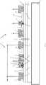
- a device useful for understanding the inventionis shown in figure 1 . On a base substrate 1, e.g.
- the III-nitride stackis present, consisting of one or more buffer layers 2, a GaN channel layer 3 and an AlGaN barrier layer 4.
- the 2DEG 5is formed at or near the interface between the channel layer and the barrier layer.
- the buffer layer 2may be constituted by several (Al)GaN layers. It improves the buffer breakdown of the device, minimizes the mismatch between the substrate 1 and the GaN layer 3, and improves the confinement of the 2DEG at the AlGaN/GaN interface.
- the diode 10comprises a central anode 11 and symmetrically placed and externally interconnected cathodes 12.
- the anode and cathodesare elongate electrodes of a given width in the direction perpendicular to the drawing in figure 1 .
- the anode and cathodesare connected to external terminals A and C respectively.
- the cathodemay also be a single electrode surrounding the anode, or the diode may have an asymmetrical structure with one anode and one cathode arranged side by side.
- a dielectric layer 13separates the anode and cathodes electrically from each other.
- the cathodes 12are joined to the barrier layer 4 through ohmic contact junction 14.
- the anodecomprises a central portion 15 that is joined to the barrier layer 4 through a Schottky barrier contact junction 16.
- the anode 11further comprises lateral portions 17 that are separated from said barrier layer by a layer 18.
- Thisis a layer of p-doped GaN or p-doped AlGaN (we'll refer to it as a 'p-GaN layer' after this).
- the p-dopingmeans that positive doping elements have been added to the GaN or AlGaN material.
- the p-doped layer applied in the inventionis thus a layer with a higher doping level than an unintentionally doped layer, i.e. a layer containing unintentional impurities (e.g. oxygen and carbon), which are typically present at a doping level below 10 13 at/cm 3 , and without intentionally added dopant atoms (typically Mg for positive doping).
- the effect of the p-doped areais to deplete the 2DEG layer when the diode is reverse biased, thereby blocking the reverse leakage current, whilst a high current conduction and low on-state voltage is obtained in forward conduction mode, through the Schottky junction 16.
- the effect of such a laterally placed p-doped regionis known in itself, as illustrated for example by US2012/0146093 .
- the HEMT 20comprises source and drain electrodes 21 and 22, in ohmic contact with the barrier layer 4, and a gate electrode 23.
- the electrodesare connected to external terminals S/D/C.
- Dielectric layers 24isolate the electrodes from each other.
- a deeper isolation area 25isolates the diode 10 from the HEMT 20.
- the gate electrode 23is separated from the barrier layer 4 by a p-GaN or p-AlGaN layer 26 (again, we'll refer to it after this as a 'p-GaN layer').
- the thickness of this layer 26is different from the thickness of the p-GaN layers 18 provided in the diode structure.
- the p-GaN layer 26 at the HEMT gateis thicker than the p-GaN layers 18 of the diode, thereby obtaining a predefined threshold voltage of the HEMT in accordance with the operative requirements of this HEMT device (conducting above a given gate bias voltage), while the turn-on voltage of the diode is lower due to a thinner p-GaN layer 18.
- the p-GaN layer 18shields the Schottky Barrier Diode from high reverse electric fields, by pinching off the channel when the anode-to-cathode voltage is lower than the turn-on voltage.
- the p-GaN area 26can pinch-off the transistor channel and allow transistor turn-off when the gate-to-source voltage is lower than the threshold voltage. Since the diode has to be a shorted connection in the on-state, a turn-on voltage as close as possible to zero is ideally targeted for the diode. Instead, a positive threshold voltage is wanted for the transistor, which must preferably show enhancement-mode behaviour (i.e. no 2DEG underneath the gate 23 unless a positive voltage is applied between the gate and source).
- the diode turn-on voltagemust be lower than the transistor threshold voltage.
- all of the electrodes, p-GaN layers and dielectric isolation layersare shaped as elongate portions having a given width measured in the direction perpendicular to the drawing, and a given length in the plane of drawing and perpendicular to the width.
- the term 'length'is used as this particular dimension corresponds to the direction of current flow in the respective devices 10 and 20.
- the length D2 of the layer 26is smaller than the length D1 of the layers 18. This aspect is related to the preferred method according to the invention as described hereafter.
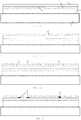
- the method of the invention for producing the device shown in figure 1comprises the following steps, illustrated in figures 2a to 2i :
- the openings 31-36are not etched at the same time, nor are all the electrodes formed simultaneously.
- the openings 32 and 35are formed first ( fig. 2c ), followed by the deposition of the p-GaN layers 18 and 26 ( fig. 2d ).
- opening 31is formed ( fig. 2e ), followed by the deposition of electrodes 11 and 23 which could be made of different metals ( fig 2f ).
- a second litho/etchis performed for forming the openings 33, 34 and 36 ( fig. 2g ). This is followed by the production of the cathode electrode 12 and source and drain electrodes 21/22 in said openings ( fig. 2h ), and the formation of the isolation area 25 ( fig. 2i ).
- the step of producing said first and second p-GaN layers 18/26is performed in a single step, by selective deposition of the p-GaN in the openings 32/35 corresponding to the second anode portion and the HEMT gate.
- the selective depositionmay be performed according to the known SAG technique (Selective Area Growth), with the dielectric layer 30 acting as the SAG mask.
- the length D1 and D2 of the openings 32 and 35is designed to obtain said different thicknesses.
- the thickness of a selectively deposited p-GaN layeris thicker than the p-GaN deposited in a wider opening due to a loading effect during selective deposition. This tuning of the p-GaN thickness by a well-considered design of the dimensions of the openings is not known in the art today.
- the structure shown in figure 1comprises active areas (such as anode, cathode and S/G/D electrodes) and separating isolation areas (13,24,25) of a given length, which is a commonly used layout for this type of device.
- active areassuch as anode, cathode and S/G/D electrodes
- isolation areas13,24,25
- the figureshows only one electrode of each type (except the cathode), but the device may consist of several electrode 'fingers' interconnected laterally by contact pads, as known in the art.
- the inventionis furthermore not limited to producing this elongate shape of the electrodes but it is relevant to producing any other device structure.
- the inventionis not limited to producing the symmetric diode structure shown in figure 1 , with a central anode and two cathodes.
- the diodemay have one anode and one cathode with the p-GaN area 18 between the Schottky junction 16 of the diode and the ohmic junction 14 of the cathode.
- the inventionis furthermore not limited to producing the anode-structure shown in figure 1 , wherein the Schottky junction 16 is separated from the p-GaN layers 18 by a dielectric area 50.
- the p-GaN layer 18may be directly adjacent and in contact with the Schottky junction 16.
- the description of a layer being deposited or produced 'on' another layer or substrateincludes the options of
Landscapes
- Electrodes Of Semiconductors (AREA)
- Junction Field-Effect Transistors (AREA)
- Chemical & Material Sciences (AREA)
- Engineering & Computer Science (AREA)
- Materials Engineering (AREA)
Description
- The present invention is related to semiconductor processing, in particular to processing of devices comprising a stack of III-nitride layers of different bandgaps, wherein charge carriers move in a 2-dimensional electron gas (2DEG) layer. The invention is in particular related to a method of producing a device comprising a Schottky diode and a High Electron Mobility Transistor (HEMT).
- Metal-semiconductor diodes, also referred to as Schottky diodes are widely used in rectifying circuits because of their low forward voltage drop and fast switching action. Schottky diodes produced on AlGaN/GaN heterostructures benefit from the high breakdown voltage of the GaN and the high mobility and high electron density of the 2DEG-layer appearing between the GaN and the AlGaN layer as a result of the difference of piezoelectric and spontaneous polarization. There is however the problem of high leakage current when the diode is reverse biased, with high power losses as a consequence. Another problem occurs when a Schottky diode of the above-described type is integrated on one substrate together with a High-Electron-Mobility Transistor (HEMT), that uses the same 2DEG for conducting charge. For a power diode, a lower turn-on voltage is desirable, in order to minimize the on-state voltage drop. However, a higher threshold voltage may be desirable for the AlGaN/GaN HEMT, which renders the diode/HEMT integration difficult.
- Patent application
US 2011/0233615 A1 discloses a GaN-based device comprising a transistor element and a rectifying element. Control electrodes of the rectifying element and of the transistor may comprise p-doped semiconductor material of different thicknesses. - Patent application
US 2001/0254056 A1 also discloses a GaN-based device comprising a transistor and a rectifier. At least some of the control electrodes may comprise p-type semiconductor material of different thicknesses. - Patent application
US 2011/0042719 A1 discloses a method of manufacturing GaN-based transistors comprising etching an opening into an insulating layer above an electron supply layer and growing p-type semiconductor material which forms part of a gate electrode. - The invention is related to a method for producing a semiconductor device comprising a Schottky diode and a High Electron Mobility Transistor, the method comprising the steps of :
- producing a III-nitride stack on a
carrier substrate 1, said stack comprising at least a lower and an upper III-nitride layer forming a heterojunction there between, so that a 2DEG layer may be formed in the lower of the two layers, - Depositing a dielectric layer on said III-nitride stack,
- Patterning said dielectric layer to form a plurality of openings through the dielectric layer, corresponding to the location of the anode and cathode electrodes of the Schottky diode and to the location of the source, drain and gate electrodes of the HEMT, wherein the opening or openings corresponding to the location of said anode, hereafter referred to as 'anode-opening(s)', comprise a first portion corresponding to the Schottky junction of said diode and a second portion adjacent to said first portion, each opening of said second portion being located between the first portion and one of the opening or openings corresponding to the cathode electrode,
- Producing a first layer or layers of a doped III-nitride material in said second portion of the anode-opening or openings, and producing a second layer or layers of a doped III-nitride material in the opening or openings corresponding to the gate of said HEMT, hereafter referred to as 'gate opening(s)', wherein the thickness of said first and second layers (18,26) is not equal,
- Producing said anode and cathode electrodes and said source, gate and drain electrodes, a portion or portions of said anode being produced on top of said first layer or layers of a doped III-nitride material and the gate electrode being produced on top of said second layer or layers of a doped III-nitride material,
- Producing an isolation area between the diode and the HEMT.
- According to the invention, the step of producing said first and second layers of a doped III-nitride material is performed by selectively depositing a doped III-nitride material in said second portion of the anode-opening(s), and in the gate opening(s), said selective deposition taking place in a single deposition step, and wherein the dimensions of said second portion of the anode opening(s) and the dimensions of the gate-opening(s) are selected so that the thickness of the obtained first layer(s) is not equal to the thickness of the obtained second layer(s).
- According to an embodiment, said openings of the second portion of the anode-opening(s) and said gate opening(s) have a length and wherein the length of said gate-opening(s) is smaller than the length of the opening(s) of said second portion of the anode opening(s), so that the thickness of said second layer (s) is higher than the thickness of said first layer(s).
- According to an embodiment of the method, following the step of depositing a dielectric layer on the III nitride stack, the following subsequent steps are performed :
- forming said second portion of the anode-opening(s), and said gate opening(s) in a first step of patterning said dielectric layer,
- producing said first and second layer of doped III-nitride material in said second portion of the anode-opening(s), and in said gate opening(s),
- forming in a second patterning step said first portion of the opening(s) corresponding to the location of the anode of the Schottky diode,
- producing said anode electrode and said gate electrode,
- forming in one or more further patterning steps said openings corresponding to the location of the cathode electrode of the Schottky diode and of the source and drain electrodes of the HEMT,
- Producing said cathode electrode and said source and drain electrodes.
- According to an embodiment, said lower III-nitride layer is a GaN layer, said upper III-nitride layer is an AlGaN layer, and said layers of doped III-nitride material are layers of p-doped GaN or AlGaN.
Figure 1 illustrates the structure of a device useful for understanding the present invention.Figures 2a to 2i illustrate a number of steps in the method according to an embodiment of the invention.- In a semiconductor device useful for understanding the invention, a Schottky power diode and a HEMT are arranged on the same substrate, and on the same stack of III-nitride materials, so as to conduct current via (portions of) the same 2DEG layers formed in said stack. In this detailed description, the 2DEG is described as formed between a GaN channel layer and a AlGaN barrier layer, even though other combinations of III-nitride layers may be suitable for the purpose of the invention. A device useful for understanding the invention is shown in
figure 1 . On abase substrate 1, e.g. a Si or Si-carbide substrate, the III-nitride stack is present, consisting of one ormore buffer layers 2, a GaNchannel layer 3 and anAlGaN barrier layer 4. The2DEG 5 is formed at or near the interface between the channel layer and the barrier layer. Thebuffer layer 2 may be constituted by several (Al)GaN layers. It improves the buffer breakdown of the device, minimizes the mismatch between thesubstrate 1 and theGaN layer 3, and improves the confinement of the 2DEG at the AlGaN/GaN interface. - The
diode 10 comprises acentral anode 11 and symmetrically placed and externally interconnectedcathodes 12. The anode and cathodes are elongate electrodes of a given width in the direction perpendicular to the drawing infigure 1 . The anode and cathodes are connected to external terminals A and C respectively. Instead of separate and externally connectedcathode portions 12, the cathode may also be a single electrode surrounding the anode, or the diode may have an asymmetrical structure with one anode and one cathode arranged side by side. - A
dielectric layer 13 separates the anode and cathodes electrically from each other. Thecathodes 12 are joined to thebarrier layer 4 throughohmic contact junction 14. The anode comprises acentral portion 15 that is joined to thebarrier layer 4 through a Schottkybarrier contact junction 16. Theanode 11 further compriseslateral portions 17 that are separated from said barrier layer by alayer 18. This is a layer of p-doped GaN or p-doped AlGaN (we'll refer to it as a 'p-GaN layer' after this). The p-doping means that positive doping elements have been added to the GaN or AlGaN material. The p-doped layer applied in the invention is thus a layer with a higher doping level than an unintentionally doped layer, i.e. a layer containing unintentional impurities (e.g. oxygen and carbon), which are typically present at a doping level below 1013 at/cm3, and without intentionally added dopant atoms (typically Mg for positive doping). The effect of the p-doped area is to deplete the 2DEG layer when the diode is reverse biased, thereby blocking the reverse leakage current, whilst a high current conduction and low on-state voltage is obtained in forward conduction mode, through theSchottky junction 16. The effect of such a laterally placed p-doped region is known in itself, as illustrated for example byUS2012/0146093 . - The HEMT 20 comprises source and
drain electrodes barrier layer 4, and agate electrode 23. The electrodes are connected to external terminals S/D/C.Dielectric layers 24 isolate the electrodes from each other. Adeeper isolation area 25 isolates thediode 10 from the HEMT 20. Thegate electrode 23 is separated from thebarrier layer 4 by a p-GaN or p-AlGaN layer 26 (again, we'll refer to it after this as a 'p-GaN layer'). The thickness of thislayer 26 is different from the thickness of the p-GaN layers 18 provided in the diode structure. This difference in thickness is important for understanding the invention, as it is related to the turn-on voltage of the diode and the threshold voltage of the HEMT. By tuning these thicknesses in a suitable way, optimized turn-on and threshold voltages of the diode and HEMT respectively can be obtained. In the device illustrated infigure 1 , the p-GaN layer 26 at the HEMT gate is thicker than the p-GaN layers 18 of the diode, thereby obtaining a predefined threshold voltage of the HEMT in accordance with the operative requirements of this HEMT device (conducting above a given gate bias voltage), while the turn-on voltage of the diode is lower due to a thinner p-GaN layer 18. - The p-
GaN layer 18 shields the Schottky Barrier Diode from high reverse electric fields, by pinching off the channel when the anode-to-cathode voltage is lower than the turn-on voltage. Similarly, the p-GaN area 26 can pinch-off the transistor channel and allow transistor turn-off when the gate-to-source voltage is lower than the threshold voltage. Since the diode has to be a shorted connection in the on-state, a turn-on voltage as close as possible to zero is ideally targeted for the diode. Instead, a positive threshold voltage is wanted for the transistor, which must preferably show enhancement-mode behaviour (i.e. no 2DEG underneath thegate 23 unless a positive voltage is applied between the gate and source). Thus, the diode turn-on voltage must be lower than the transistor threshold voltage. In both cases, it is possible to tune the turn-on/threshold voltage by modifying the p-GaN thickness: increasing the p-GaN layer thickness results into a positive shift of turn-on/threshold voltage. - In the device of
figure 1 , all of the electrodes, p-GaN layers and dielectric isolation layers are shaped as elongate portions having a given width measured in the direction perpendicular to the drawing, and a given length in the plane of drawing and perpendicular to the width. The term 'length' is used as this particular dimension corresponds to the direction of current flow in therespective devices figure 1 , the length D2 of thelayer 26 is smaller than the length D1 of thelayers 18. This aspect is related to the preferred method according to the invention as described hereafter. - In general terms, the method of the invention for producing the device shown in
figure 1 (with an AlGaN/GaN stack and layers 18 and 26 referred to as 'p-GaN layers', although the method is not limited to these particular combinations), comprises the following steps, illustrated infigures 2a to 2i : - producing a III-
nitride stack 2/3/4 as described above, on acarrier substrate 1. The production of such a III-nitride stack can be done according to any suitable technique known in the art, e.g. by Metal Organic Chemical Vapour Deposition (MOCVD). Thebarrier layer 4 is the top layer of the stack. - Depositing a
dielectric layer 30 on said III-nitride stack, for example a Si3N4 layer deposited in-situ (in the same process chamber as the III-nitride stack deposition) and for example by the same deposition process as the III-nitride stack. The dielectric layer may consist of several layers deposited sequentially. - Patterning (e.g. by one or more standard litho/etch steps) said dielectric layer to form a plurality of
openings 31 to 36 through the dielectric layer, corresponding to thelocations 31 to 33 of the anode and cathode electrodes of theSchottky diode 10 and to thelocations 34/35/36 of the source, gate and drain electrodes of theHEMT 20, wherein the opening or openings corresponding to said anode comprise afirst portion 31 corresponding to the Schottky junction of said diode and at least onesecond portion 32 adjacent to said first portion, and located between thefirst portion 31 and the opening oropenings 33 corresponding to the cathode. These openings are preferably not patterned in one litho/etch step, but in a series of such steps as described further in this description. - Producing a
first layer 18 of p-GaN in saidsecond portion 32 of the anode-opening or openings, and producing a second layer of p-GaN 26 in the opening oropenings 35 corresponding to the gate of said HEMT, wherein the thickness of said first and second layers is not equal, - Producing said electrodes, for example by depositing electrically conductive layers and patterning said layers, a portion of said
anode 11 being produced on top of the first p-GaN layer 18 and thegate electrode 23 being produced on top of the second p-GaN layer 26. Again, all electrodes are preferably not produced in a single step, but some electrodes may be produced after one or more first litho/etch steps, with other electrodes produced after further litho/etch steps, as described in the case of a preferred embodiment further in this description. - Producing an
isolation area 25 between the diode and the HEMT, e.g. produced by a mesa etch technique. - According to the preferred embodiment illustrated in
figure 2 , the openings 31-36 are not etched at the same time, nor are all the electrodes formed simultaneously. Theopenings fig. 2c ), followed by the deposition of the p-GaN layers 18 and 26 (fig. 2d ). Then opening 31 is formed (fig. 2e ), followed by the deposition ofelectrodes fig 2f ). Then a second litho/etch is performed for forming theopenings fig. 2g ). This is followed by the production of thecathode electrode 12 and source and drainelectrodes 21/22 in said openings (fig. 2h ), and the formation of the isolation area 25 (fig. 2i ). - According to the invention, the step of producing said first and second p-
GaN layers 18/26 is performed in a single step, by selective deposition of the p-GaN in theopenings 32/35 corresponding to the second anode portion and the HEMT gate. The selective deposition may be performed according to the known SAG technique (Selective Area Growth), with thedielectric layer 30 acting as the SAG mask. - Since the p-
GaN layers 18/26 are deposited by simultaneous selective deposition as described above, the length D1 and D2 of theopenings - The structure shown in
figure 1 comprises active areas (such as anode, cathode and S/G/D electrodes) and separating isolation areas (13,24,25) of a given length, which is a commonly used layout for this type of device. The figure shows only one electrode of each type (except the cathode), but the device may consist of several electrode 'fingers' interconnected laterally by contact pads, as known in the art. The invention is furthermore not limited to producing this elongate shape of the electrodes but it is relevant to producing any other device structure. - The invention is not limited to producing the symmetric diode structure shown in
figure 1 , with a central anode and two cathodes. The diode may have one anode and one cathode with the p-GaN area 18 between theSchottky junction 16 of the diode and theohmic junction 14 of the cathode. - The invention is furthermore not limited to producing the anode-structure shown in
figure 1 , wherein theSchottky junction 16 is separated from the p-GaN layers 18 by adielectric area 50. In an alternative device produced by the inventive method, the p-GaN layer 18 may be directly adjacent and in contact with theSchottky junction 16. - While the invention has been illustrated and described in detail in the drawings and foregoing description, such illustration and description are to be considered illustrative or exemplary and not restrictive. Other variations to the disclosed embodiments can be understood and effected by those skilled in the art in practicing the claimed invention, from a study of the drawings, the disclosure and the appended claims. In the claims, the word "comprising" does not exclude other elements or steps, and the indefinite article "a" or "an" does not exclude a plurality. The mere fact that certain measures are recited in mutually different dependent claims does not indicate that a combination of these measures cannot be used to advantage. Any reference signs in the claims should not be construed as limiting the scope.
- The foregoing description details certain embodiments of the invention. It will be appreciated, however, that no matter how detailed the foregoing appears in text, the invention may be practiced in many ways, and is therefore not limited to the embodiments disclosed. It should be noted that the use of particular terminology when describing certain features or aspects of the invention should not be taken to imply that the terminology is being re-defined herein to be restricted to include any specific characteristics of the features or aspects of the invention with which that terminology is associated.
- Unless specifically specified, the description of a layer being deposited or produced 'on' another layer or substrate, includes the options of
- said layer being produced or deposited directly on, i.e. in contact with, said other layer or substrate, and
- said layer being produced on one or a stack of intermediate layers between said layer and said other layer or substrate.
Claims (4)
- A method for producing a semiconductor device comprising a Schottky diode (10) and a High Electron Mobility Transistor (20), the method comprising the steps of :- producing a III-nitride stack (2,3,4) on a carrier substrate 1, said stack comprising at least a lower and an upper III-nitride layer (3,4) forming a heterojunction there between, so that a 2DEG layer (5) may be formed in the lower of the two layers,- Depositing a dielectric layer (30) on said III-nitride stack,- Patterning said dielectric layer to form a plurality of openings through the dielectric layer, corresponding to the location (31,32,33) of the anode and cathode electrodes of the Schottky diode (10) and to the location (34,35,36) of the source, drain and gate electrodes of the HEMT (30), wherein the opening or openings corresponding to the location of said anode, hereafter referred to as 'anode-opening(s)', comprise a first portion (31) corresponding to the Schottky junction (16) of said diode and a second portion (32) adjacent to said first portion, each opening of said second portion (32) being located between the first portion (31) and one of the opening or openings (33) corresponding to the cathode electrode,- Producing a first layer or layers (18) of a doped III-nitride material in said second portion (32) of the anode-opening or openings, and producing a second layer or layers (26) of a doped III-nitride material in the opening or openings (35) corresponding to the gate of said HEMT, hereafter referred to as 'gate opening (s)', wherein the thickness of said first and second layers (18,26) is not equal,- Producing said anode and cathode electrodes (11,12) and said source, gate and drain electrodes (21,23,22), a portion or portions (17) of said anode being produced on top of said first layer or layers (18) of a doped III-nitride material and the gate electrode being produced on top of said second layer or layers (26) of a doped III-nitride material,- Producing an isolation area (25) between the diode and the HEMT,wherein the step of producing said first and second layers (18,26) of a doped III-nitride material is performed by selectively depositing a doped III-nitride material in said second portion (32) of the anode-opening(s), and in the gate opening(s) (35), said selective deposition taking place in a single deposition step, and wherein the dimensions of said second portion (32) of the anode opening (s) and the dimensions of the gate-opening (s) (35) are selected so that the thickness of the obtained first layer(s) (18) is not equal to the thickness of the obtained second layer(s) (26).
- Method according to claim 1, wherein said openings of the second portion (32) of the anode-opening(s) and said gate opening(s) (35) have a length and wherein the length (D2) of said gate-opening (s) (35) is smaller than the length (D1) of the opening (s) of said second portion (32) of the anode opening(s), so that the thickness of said second layer (s) (26) is higher than the thickness of said first layer(s) (18).
- Method according to any one of claims 1 and 2, wherein following the step of depositing a dielectric layer (30) on the III nitride stack, the following subsequent steps are performed :- forming said second portion (32) of the anode-opening(s), and said gate opening(s) (35) in a first step of patterning said dielectric layer (30),- producing said first and second layer (18,26) of doped III-nitride material in said second portion (32) of the anode-opening(s), and in said gate opening(s) (35),- forming in a second patterning step said first portion (31) of the opening(s) corresponding to the location of the anode of the Schottky diode (10)- producing said anode electrode (11) and said gate electrode (23),- forming in one or more further patterning steps said openings (33,34,36) corresponding to the location of the cathode electrode of the Schottky diode (10) and of the source and drain electrodes of the HEMT (20),- Producing said cathode electrode (12) and said source and drain electrodes (21,22).
- Method according to any one of claims 1 to 3, wherein said lower III-nitride layer (3) is a GaN layer, said upper III-nitride layer is an AlGaN layer (4), and said layers of doped III-nitride material (18,26) are layers of p-doped GaN or AlGaN.
Priority Applications (4)
| Application Number | Priority Date | Filing Date | Title |
|---|---|---|---|
| EP13163861.1AEP2793255B8 (en) | 2013-04-16 | 2013-04-16 | Manufacturing method of a semiconductor device comprising a schottky diode and a high electron mobility transistor |
| JP2014079460AJP6280796B2 (en) | 2013-04-16 | 2014-04-08 | Manufacturing method of semiconductor device having Schottky diode and high electron mobility transistor |
| US14/254,615US9276082B2 (en) | 2013-04-16 | 2014-04-16 | Method for producing a semiconductor device comprising a Schottky diode and a high electron mobility transistor |
| US14/682,958US9431511B2 (en) | 2013-04-16 | 2015-04-09 | Method for producing a semiconductor device comprising a Schottky diode and a high electron mobility transistor |
Applications Claiming Priority (1)
| Application Number | Priority Date | Filing Date | Title |
|---|---|---|---|
| EP13163861.1AEP2793255B8 (en) | 2013-04-16 | 2013-04-16 | Manufacturing method of a semiconductor device comprising a schottky diode and a high electron mobility transistor |
Publications (3)
| Publication Number | Publication Date |
|---|---|
| EP2793255A1 EP2793255A1 (en) | 2014-10-22 |
| EP2793255B1true EP2793255B1 (en) | 2017-12-06 |
| EP2793255B8 EP2793255B8 (en) | 2018-01-17 |
Family
ID=48095727
Family Applications (1)
| Application Number | Title | Priority Date | Filing Date |
|---|---|---|---|
| EP13163861.1AActiveEP2793255B8 (en) | 2013-04-16 | 2013-04-16 | Manufacturing method of a semiconductor device comprising a schottky diode and a high electron mobility transistor |
Country Status (3)
| Country | Link |
|---|---|
| US (2) | US9276082B2 (en) |
| EP (1) | EP2793255B8 (en) |
| JP (1) | JP6280796B2 (en) |
Families Citing this family (34)
| Publication number | Priority date | Publication date | Assignee | Title |
|---|---|---|---|---|
| US9449833B1 (en) | 2010-06-02 | 2016-09-20 | Hrl Laboratories, Llc | Methods of fabricating self-aligned FETS using multiple sidewall spacers |
| US8946724B1 (en)* | 2010-06-02 | 2015-02-03 | Hrl Laboratories, Llc | Monolithically integrated self-aligned GaN-HEMTs and Schottky diodes and method of fabricating the same |
| DE112014003175B4 (en)* | 2013-07-08 | 2020-12-03 | Efficient Power Conversion Corporation | Process for producing self-aligning insulation in gallium nitride components and integrated circuits |
| US20150372096A1 (en)* | 2014-06-20 | 2015-12-24 | Ishiang Shih | High Electron Mobility Transistors and Integrated Circuits with Improved Feature Uniformity and Reduced defects for Microwave and Millimetre Wave Applications |
| JP2016018939A (en)* | 2014-07-10 | 2016-02-01 | 株式会社豊田中央研究所 | Schottky barrier diode formed on nitride semiconductor substrate |
| JP6055799B2 (en)* | 2014-07-29 | 2016-12-27 | 株式会社豊田中央研究所 | Semiconductor device and manufacturing method thereof |
| WO2017027704A1 (en)* | 2015-08-11 | 2017-02-16 | Cambridge Electronics, Inc. | Semiconductor structure with a spacer layer |
| US10651317B2 (en) | 2016-04-15 | 2020-05-12 | Macom Technology Solutions Holdings, Inc. | High-voltage lateral GaN-on-silicon Schottky diode |
| US20170301780A1 (en) | 2016-04-15 | 2017-10-19 | Macom Technology Solutions Holdings, Inc. | High-voltage gan high electron mobility transistors with reduced leakage current |
| US10170611B1 (en) | 2016-06-24 | 2019-01-01 | Hrl Laboratories, Llc | T-gate field effect transistor with non-linear channel layer and/or gate foot face |
| CN106783869B (en)* | 2016-09-07 | 2019-11-22 | 武汉华星光电技术有限公司 | Thin film transistor array substrate and manufacturing method thereof |
| CN106449747A (en)* | 2016-11-28 | 2017-02-22 | 电子科技大学 | Reverse blocked gallium nitride high-electron-mobility transistor |
| US10854718B2 (en)* | 2017-02-21 | 2020-12-01 | Semiconductor Components Industries, Llc | Method of forming a semiconductor device |
| DE112017007912T5 (en)* | 2017-09-29 | 2020-07-02 | Intel Corporation | GROUP III NITRIDE ANTENNA DIODE |
| WO2019066975A1 (en)* | 2017-09-29 | 2019-04-04 | Intel Corporation | Group iii-nitride silicon controlled rectifier |
| WO2019066972A1 (en)* | 2017-09-29 | 2019-04-04 | Intel Corporation | Group iii-nitride schottky diode |
| CN108022925B (en)* | 2017-11-06 | 2020-09-15 | 中国科学院微电子研究所 | GaN-based monolithic power converter and manufacturing method thereof |
| US11056483B2 (en) | 2018-01-19 | 2021-07-06 | Macom Technology Solutions Holdings, Inc. | Heterolithic microwave integrated circuits including gallium-nitride devices on intrinsic semiconductor |
| US11233047B2 (en) | 2018-01-19 | 2022-01-25 | Macom Technology Solutions Holdings, Inc. | Heterolithic microwave integrated circuits including gallium-nitride devices on highly doped regions of intrinsic silicon |
| US10950598B2 (en)* | 2018-01-19 | 2021-03-16 | Macom Technology Solutions Holdings, Inc. | Heterolithic microwave integrated circuits including gallium-nitride devices formed on highly doped semiconductor |
| US10868162B1 (en) | 2018-08-31 | 2020-12-15 | Hrl Laboratories, Llc | Self-aligned gallium nitride FinFET and method of fabricating the same |
| WO2021149599A1 (en)* | 2020-01-24 | 2021-07-29 | ローム株式会社 | Method for manufacturing nitride semiconductor device and nitride semiconductor device |
| WO2021195506A1 (en) | 2020-03-26 | 2021-09-30 | Macom Technology Solutions Holdings, Inc. | Microwave integrated circuits including gallium-nitride devices on silicon |
| CN112154542B (en)* | 2020-04-29 | 2023-12-08 | 英诺赛科(珠海)科技有限公司 | Electronic device |
| JP7553770B2 (en)* | 2020-05-28 | 2024-09-19 | 日亜化学工業株式会社 | Method for manufacturing a field effect transistor |
| CN114078965B (en) | 2020-08-11 | 2023-08-08 | 联华电子股份有限公司 | High electron mobility transistor and manufacturing method thereof |
| KR102427421B1 (en)* | 2020-08-28 | 2022-08-01 | 주식회사 시지트로닉스 | Structure and Fabrication Method of the Wide Band Gap Semiconductor Device with High Performance Rectifying |
| EP4272254A4 (en)* | 2021-03-05 | 2024-03-06 | Huawei Technologies Co., Ltd. | GALLIUM NITRIDE POWER TRANSISTOR |
| JP2022184315A (en)* | 2021-06-01 | 2022-12-13 | 株式会社東芝 | semiconductor equipment |
| WO2023272674A1 (en)* | 2021-07-01 | 2023-01-05 | Innoscience (Suzhou) Technology Co., Ltd. | Nitride-based multi-channel switching semiconductor device and method for manufacturing the same |
| US12396232B2 (en)* | 2021-08-27 | 2025-08-19 | Intel Corporation | III-N diodes with n-doped wells and capping layers |
| CN113690311B (en)* | 2021-08-30 | 2023-04-25 | 电子科技大学 | GaN HEMT device integrated with flywheel diode |
| CN114207818A (en)* | 2021-11-12 | 2022-03-18 | 英诺赛科(苏州)科技有限公司 | Nitride-based semiconductor device and method of making the same |
| CN115000064B (en)* | 2022-05-23 | 2025-07-29 | 西安电子科技大学 | Multi-path control composite function device |
Family Cites Families (10)
| Publication number | Priority date | Publication date | Assignee | Title |
|---|---|---|---|---|
| JP2007109830A (en)* | 2005-10-12 | 2007-04-26 | Univ Nagoya | Field effect transistor |
| JP2008078526A (en)* | 2006-09-25 | 2008-04-03 | New Japan Radio Co Ltd | Nitride semiconductor device and its manufacturing method |
| US7767508B2 (en)* | 2006-10-16 | 2010-08-03 | Advanced Micro Devices, Inc. | Method for forming offset spacers for semiconductor device arrangements |
| JP2009164158A (en)* | 2007-12-28 | 2009-07-23 | Panasonic Corp | Semiconductor device and manufacturing method thereof |
| JP2009231395A (en)* | 2008-03-19 | 2009-10-08 | Sumitomo Chemical Co Ltd | Semiconductor device and method for manufacturing semiconductor device |
| JP5530682B2 (en) | 2009-09-03 | 2014-06-25 | パナソニック株式会社 | Nitride semiconductor device |
| JP2011165749A (en)* | 2010-02-05 | 2011-08-25 | Panasonic Corp | Semiconductor device |
| JP5056883B2 (en)* | 2010-03-26 | 2012-10-24 | サンケン電気株式会社 | Semiconductor device |
| JP5672756B2 (en)* | 2010-04-16 | 2015-02-18 | サンケン電気株式会社 | Semiconductor device |
| CN103329273B (en)* | 2011-01-17 | 2016-03-09 | 富士通株式会社 | Semiconductor device and manufacture method thereof |
- 2013
- 2013-04-16EPEP13163861.1Apatent/EP2793255B8/enactiveActive
- 2014
- 2014-04-08JPJP2014079460Apatent/JP6280796B2/enactiveActive
- 2014-04-16USUS14/254,615patent/US9276082B2/enactiveActive
- 2015
- 2015-04-09USUS14/682,958patent/US9431511B2/enactiveActive
Non-Patent Citations (1)
| Title |
|---|
| None* |
Also Published As
| Publication number | Publication date |
|---|---|
| EP2793255A1 (en) | 2014-10-22 |
| US9276082B2 (en) | 2016-03-01 |
| US20150214327A1 (en) | 2015-07-30 |
| JP6280796B2 (en) | 2018-02-14 |
| US9431511B2 (en) | 2016-08-30 |
| US20140306235A1 (en) | 2014-10-16 |
| JP2014212316A (en) | 2014-11-13 |
| EP2793255B8 (en) | 2018-01-17 |
Similar Documents
| Publication | Publication Date | Title |
|---|---|---|
| EP2793255B1 (en) | Manufacturing method of a semiconductor device comprising a schottky diode and a high electron mobility transistor | |
| US10707203B2 (en) | Cascode semiconductor device structure and method therefor | |
| EP2722890B1 (en) | Schottky diode structure and method of fabrication | |
| US9570438B1 (en) | Avalanche-rugged quasi-vertical HEMT | |
| US9960154B2 (en) | GaN structures | |
| JP6754782B2 (en) | Semiconductor device | |
| US8519439B2 (en) | Nitride semiconductor element with N-face semiconductor crystal layer | |
| US9589951B2 (en) | High-electron-mobility transistor with protective diode | |
| JP5578873B2 (en) | Gallium nitride semiconductor device and manufacturing method thereof | |
| US9502544B2 (en) | Method and system for planar regrowth in GaN electronic devices | |
| CN110476254B (en) | Heterojunction transistor with vertical structure | |
| US20140048850A1 (en) | Semiconductor devices and methods of manufacturing the semiconductor device | |
| WO2013020051A1 (en) | Method and system for a gan vertical jfet utilizing a regrown channel | |
| US20120280281A1 (en) | Gallium nitride or other group iii/v-based schottky diodes with improved operating characteristics | |
| US11437473B2 (en) | Nitride semiconductor device and method of manufacturing the same | |
| KR20140133360A (en) | Nitride high electron mobility transistor and manufacturing method thereof | |
| US10141439B2 (en) | Semiconductor device and method of manufacturing the same | |
| WO2019163075A1 (en) | Semiconductor device | |
| EP4439677A1 (en) | Hemt device having an improved gate structure and manufacturing process thereof | |
| KR20160100524A (en) | nitride-based insulated gate bipolar transistor |
Legal Events
| Date | Code | Title | Description |
|---|---|---|---|
| PUAI | Public reference made under article 153(3) epc to a published international application that has entered the european phase | Free format text:ORIGINAL CODE: 0009012 | |
| 17P | Request for examination filed | Effective date:20130416 | |
| AK | Designated contracting states | Kind code of ref document:A1 Designated state(s):AL AT BE BG CH CY CZ DE DK EE ES FI FR GB GR HR HU IE IS IT LI LT LU LV MC MK MT NL NO PL PT RO RS SE SI SK SM TR | |
| AX | Request for extension of the european patent | Extension state:BA ME | |
| RBV | Designated contracting states (corrected) | Designated state(s):AL AT BE BG CH CY CZ DE DK EE ES FI FR GB GR HR HU IE IS IT LI LT LU LV MC MK MT NL NO PL PT RO RS SE SI SK SM TR | |
| R17P | Request for examination filed (corrected) | Effective date:20150403 | |
| GRAP | Despatch of communication of intention to grant a patent | Free format text:ORIGINAL CODE: EPIDOSNIGR1 | |
| RIC1 | Information provided on ipc code assigned before grant | Ipc:H01L 21/8252 20060101AFI20170302BHEP Ipc:H01L 29/778 20060101ALI20170302BHEP Ipc:H01L 29/66 20060101ALN20170302BHEP Ipc:H01L 29/10 20060101ALN20170302BHEP Ipc:H01L 29/20 20060101ALI20170302BHEP Ipc:H01L 29/872 20060101ALI20170302BHEP Ipc:H01L 29/06 20060101ALN20170302BHEP Ipc:H01L 27/06 20060101ALI20170302BHEP | |
| INTG | Intention to grant announced | Effective date:20170320 | |
| GRAS | Grant fee paid | Free format text:ORIGINAL CODE: EPIDOSNIGR3 | |
| GRAA | (expected) grant | Free format text:ORIGINAL CODE: 0009210 | |
| AK | Designated contracting states | Kind code of ref document:B1 Designated state(s):AL AT BE BG CH CY CZ DE DK EE ES FI FR GB GR HR HU IE IS IT LI LT LU LV MC MK MT NL NO PL PT RO RS SE SI SK SM TR | |
| REG | Reference to a national code | Ref country code:GB Ref legal event code:FG4D | |
| REG | Reference to a national code | Ref country code:AT Ref legal event code:REF Ref document number:953102 Country of ref document:AT Kind code of ref document:T Effective date:20171215 Ref country code:CH Ref legal event code:EP | |
| RAP2 | Party data changed (patent owner data changed or rights of a patent transferred) | Owner name:IMEC VZW | |
| REG | Reference to a national code | Ref country code:IE Ref legal event code:FG4D | |
| REG | Reference to a national code | Ref country code:DE Ref legal event code:R096 Ref document number:602013030308 Country of ref document:DE | |
| REG | Reference to a national code | Ref country code:FR Ref legal event code:PLFP Year of fee payment:6 | |
| REG | Reference to a national code | Ref country code:NL Ref legal event code:MP Effective date:20171206 | |
| REG | Reference to a national code | Ref country code:LT Ref legal event code:MG4D | |
| PG25 | Lapsed in a contracting state [announced via postgrant information from national office to epo] | Ref country code:SE Free format text:LAPSE BECAUSE OF FAILURE TO SUBMIT A TRANSLATION OF THE DESCRIPTION OR TO PAY THE FEE WITHIN THE PRESCRIBED TIME-LIMIT Effective date:20171206 Ref country code:LT Free format text:LAPSE BECAUSE OF FAILURE TO SUBMIT A TRANSLATION OF THE DESCRIPTION OR TO PAY THE FEE WITHIN THE PRESCRIBED TIME-LIMIT Effective date:20171206 Ref country code:FI Free format text:LAPSE BECAUSE OF FAILURE TO SUBMIT A TRANSLATION OF THE DESCRIPTION OR TO PAY THE FEE WITHIN THE PRESCRIBED TIME-LIMIT Effective date:20171206 Ref country code:NO Free format text:LAPSE BECAUSE OF FAILURE TO SUBMIT A TRANSLATION OF THE DESCRIPTION OR TO PAY THE FEE WITHIN THE PRESCRIBED TIME-LIMIT Effective date:20180306 Ref country code:ES Free format text:LAPSE BECAUSE OF FAILURE TO SUBMIT A TRANSLATION OF THE DESCRIPTION OR TO PAY THE FEE WITHIN THE PRESCRIBED TIME-LIMIT Effective date:20171206 | |
| REG | Reference to a national code | Ref country code:AT Ref legal event code:MK05 Ref document number:953102 Country of ref document:AT Kind code of ref document:T Effective date:20171206 | |
| PG25 | Lapsed in a contracting state [announced via postgrant information from national office to epo] | Ref country code:GR Free format text:LAPSE BECAUSE OF FAILURE TO SUBMIT A TRANSLATION OF THE DESCRIPTION OR TO PAY THE FEE WITHIN THE PRESCRIBED TIME-LIMIT Effective date:20180307 Ref country code:RS Free format text:LAPSE BECAUSE OF FAILURE TO SUBMIT A TRANSLATION OF THE DESCRIPTION OR TO PAY THE FEE WITHIN THE PRESCRIBED TIME-LIMIT Effective date:20171206 Ref country code:HR Free format text:LAPSE BECAUSE OF FAILURE TO SUBMIT A TRANSLATION OF THE DESCRIPTION OR TO PAY THE FEE WITHIN THE PRESCRIBED TIME-LIMIT Effective date:20171206 Ref country code:LV Free format text:LAPSE BECAUSE OF FAILURE TO SUBMIT A TRANSLATION OF THE DESCRIPTION OR TO PAY THE FEE WITHIN THE PRESCRIBED TIME-LIMIT Effective date:20171206 Ref country code:BG Free format text:LAPSE BECAUSE OF FAILURE TO SUBMIT A TRANSLATION OF THE DESCRIPTION OR TO PAY THE FEE WITHIN THE PRESCRIBED TIME-LIMIT Effective date:20180306 | |
| PG25 | Lapsed in a contracting state [announced via postgrant information from national office to epo] | Ref country code:NL Free format text:LAPSE BECAUSE OF FAILURE TO SUBMIT A TRANSLATION OF THE DESCRIPTION OR TO PAY THE FEE WITHIN THE PRESCRIBED TIME-LIMIT Effective date:20171206 | |
| PG25 | Lapsed in a contracting state [announced via postgrant information from national office to epo] | Ref country code:SK Free format text:LAPSE BECAUSE OF FAILURE TO SUBMIT A TRANSLATION OF THE DESCRIPTION OR TO PAY THE FEE WITHIN THE PRESCRIBED TIME-LIMIT Effective date:20171206 Ref country code:CZ Free format text:LAPSE BECAUSE OF FAILURE TO SUBMIT A TRANSLATION OF THE DESCRIPTION OR TO PAY THE FEE WITHIN THE PRESCRIBED TIME-LIMIT Effective date:20171206 Ref country code:EE Free format text:LAPSE BECAUSE OF FAILURE TO SUBMIT A TRANSLATION OF THE DESCRIPTION OR TO PAY THE FEE WITHIN THE PRESCRIBED TIME-LIMIT Effective date:20171206 | |
| PG25 | Lapsed in a contracting state [announced via postgrant information from national office to epo] | Ref country code:PL Free format text:LAPSE BECAUSE OF FAILURE TO SUBMIT A TRANSLATION OF THE DESCRIPTION OR TO PAY THE FEE WITHIN THE PRESCRIBED TIME-LIMIT Effective date:20171206 Ref country code:IT Free format text:LAPSE BECAUSE OF FAILURE TO SUBMIT A TRANSLATION OF THE DESCRIPTION OR TO PAY THE FEE WITHIN THE PRESCRIBED TIME-LIMIT Effective date:20171206 Ref country code:RO Free format text:LAPSE BECAUSE OF FAILURE TO SUBMIT A TRANSLATION OF THE DESCRIPTION OR TO PAY THE FEE WITHIN THE PRESCRIBED TIME-LIMIT Effective date:20171206 Ref country code:AT Free format text:LAPSE BECAUSE OF FAILURE TO SUBMIT A TRANSLATION OF THE DESCRIPTION OR TO PAY THE FEE WITHIN THE PRESCRIBED TIME-LIMIT Effective date:20171206 Ref country code:SM Free format text:LAPSE BECAUSE OF FAILURE TO SUBMIT A TRANSLATION OF THE DESCRIPTION OR TO PAY THE FEE WITHIN THE PRESCRIBED TIME-LIMIT Effective date:20171206 | |
| REG | Reference to a national code | Ref country code:DE Ref legal event code:R097 Ref document number:602013030308 Country of ref document:DE | |
| PLBE | No opposition filed within time limit | Free format text:ORIGINAL CODE: 0009261 | |
| STAA | Information on the status of an ep patent application or granted ep patent | Free format text:STATUS: NO OPPOSITION FILED WITHIN TIME LIMIT | |
| 26N | No opposition filed | Effective date:20180907 | |
| PG25 | Lapsed in a contracting state [announced via postgrant information from national office to epo] | Ref country code:SI Free format text:LAPSE BECAUSE OF FAILURE TO SUBMIT A TRANSLATION OF THE DESCRIPTION OR TO PAY THE FEE WITHIN THE PRESCRIBED TIME-LIMIT Effective date:20171206 Ref country code:DK Free format text:LAPSE BECAUSE OF FAILURE TO SUBMIT A TRANSLATION OF THE DESCRIPTION OR TO PAY THE FEE WITHIN THE PRESCRIBED TIME-LIMIT Effective date:20171206 Ref country code:MC Free format text:LAPSE BECAUSE OF FAILURE TO SUBMIT A TRANSLATION OF THE DESCRIPTION OR TO PAY THE FEE WITHIN THE PRESCRIBED TIME-LIMIT Effective date:20171206 | |
| REG | Reference to a national code | Ref country code:CH Ref legal event code:PL | |
| REG | Reference to a national code | Ref country code:BE Ref legal event code:MM Effective date:20180430 | |
| GBPC | Gb: european patent ceased through non-payment of renewal fee | Effective date:20180416 | |
| REG | Reference to a national code | Ref country code:IE Ref legal event code:MM4A | |
| PG25 | Lapsed in a contracting state [announced via postgrant information from national office to epo] | Ref country code:LU Free format text:LAPSE BECAUSE OF NON-PAYMENT OF DUE FEES Effective date:20180416 | |
| PG25 | Lapsed in a contracting state [announced via postgrant information from national office to epo] | Ref country code:BE Free format text:LAPSE BECAUSE OF NON-PAYMENT OF DUE FEES Effective date:20180430 Ref country code:CH Free format text:LAPSE BECAUSE OF NON-PAYMENT OF DUE FEES Effective date:20180430 Ref country code:GB Free format text:LAPSE BECAUSE OF NON-PAYMENT OF DUE FEES Effective date:20180416 Ref country code:LI Free format text:LAPSE BECAUSE OF NON-PAYMENT OF DUE FEES Effective date:20180430 | |
| PG25 | Lapsed in a contracting state [announced via postgrant information from national office to epo] | Ref country code:IE Free format text:LAPSE BECAUSE OF NON-PAYMENT OF DUE FEES Effective date:20180416 | |
| PG25 | Lapsed in a contracting state [announced via postgrant information from national office to epo] | Ref country code:MT Free format text:LAPSE BECAUSE OF NON-PAYMENT OF DUE FEES Effective date:20180416 | |
| PG25 | Lapsed in a contracting state [announced via postgrant information from national office to epo] | Ref country code:TR Free format text:LAPSE BECAUSE OF FAILURE TO SUBMIT A TRANSLATION OF THE DESCRIPTION OR TO PAY THE FEE WITHIN THE PRESCRIBED TIME-LIMIT Effective date:20171206 | |
| PG25 | Lapsed in a contracting state [announced via postgrant information from national office to epo] | Ref country code:HU Free format text:LAPSE BECAUSE OF FAILURE TO SUBMIT A TRANSLATION OF THE DESCRIPTION OR TO PAY THE FEE WITHIN THE PRESCRIBED TIME-LIMIT; INVALID AB INITIO Effective date:20130416 Ref country code:PT Free format text:LAPSE BECAUSE OF FAILURE TO SUBMIT A TRANSLATION OF THE DESCRIPTION OR TO PAY THE FEE WITHIN THE PRESCRIBED TIME-LIMIT Effective date:20171206 | |
| PG25 | Lapsed in a contracting state [announced via postgrant information from national office to epo] | Ref country code:CY Free format text:LAPSE BECAUSE OF FAILURE TO SUBMIT A TRANSLATION OF THE DESCRIPTION OR TO PAY THE FEE WITHIN THE PRESCRIBED TIME-LIMIT Effective date:20171206 Ref country code:MK Free format text:LAPSE BECAUSE OF NON-PAYMENT OF DUE FEES Effective date:20171206 | |
| PG25 | Lapsed in a contracting state [announced via postgrant information from national office to epo] | Ref country code:AL Free format text:LAPSE BECAUSE OF FAILURE TO SUBMIT A TRANSLATION OF THE DESCRIPTION OR TO PAY THE FEE WITHIN THE PRESCRIBED TIME-LIMIT Effective date:20171206 Ref country code:IS Free format text:LAPSE BECAUSE OF FAILURE TO SUBMIT A TRANSLATION OF THE DESCRIPTION OR TO PAY THE FEE WITHIN THE PRESCRIBED TIME-LIMIT Effective date:20180406 | |
| P01 | Opt-out of the competence of the unified patent court (upc) registered | Effective date:20230513 | |
| REG | Reference to a national code | Ref country code:DE Ref legal event code:R079 Ref document number:602013030308 Country of ref document:DE Free format text:PREVIOUS MAIN CLASS: H01L0021825200 Ipc:H10D0084050000 | |
| PGFP | Annual fee paid to national office [announced via postgrant information from national office to epo] | Ref country code:FR Payment date:20250319 Year of fee payment:13 | |
| PGFP | Annual fee paid to national office [announced via postgrant information from national office to epo] | Ref country code:DE Payment date:20250319 Year of fee payment:13 |