EP2781030B1 - Perturbation-based dynamic measurement of antenna impedance in real-time - Google Patents
Perturbation-based dynamic measurement of antenna impedance in real-timeDownload PDFInfo
- Publication number
- EP2781030B1 EP2781030B1EP11791686.6AEP11791686AEP2781030B1EP 2781030 B1EP2781030 B1EP 2781030B1EP 11791686 AEP11791686 AEP 11791686AEP 2781030 B1EP2781030 B1EP 2781030B1
- Authority
- EP
- European Patent Office
- Prior art keywords
- frequency
- antenna
- received power
- matching circuit
- wireless communications
- Prior art date
- Legal status (The legal status is an assumption and is not a legal conclusion. Google has not performed a legal analysis and makes no representation as to the accuracy of the status listed.)
- Active
Links
- 238000005259measurementMethods0.000titleclaimsdescription47
- 238000004891communicationMethods0.000claimsdescription45
- 238000012545processingMethods0.000claimsdescription34
- 238000000034methodMethods0.000claimsdescription31
- 230000003595spectral effectEffects0.000claimsdescription5
- 238000012935AveragingMethods0.000claimsdescription2
- 230000006870functionEffects0.000description20
- 230000008859changeEffects0.000description9
- 230000015654memoryEffects0.000description8
- 230000008569processEffects0.000description7
- 230000001131transforming effectEffects0.000description7
- 230000001413cellular effectEffects0.000description6
- 238000010586diagramMethods0.000description6
- 238000003860storageMethods0.000description6
- 238000005516engineering processMethods0.000description5
- 125000004122cyclic groupChemical group0.000description4
- 230000003094perturbing effectEffects0.000description4
- 230000009471actionEffects0.000description3
- 230000008901benefitEffects0.000description3
- 238000004364calculation methodMethods0.000description3
- 239000003990capacitorSubstances0.000description3
- 238000006243chemical reactionMethods0.000description3
- 238000004590computer programMethods0.000description3
- 238000013461designMethods0.000description3
- 230000007613environmental effectEffects0.000description3
- 238000002847impedance measurementMethods0.000description3
- 230000010365information processingEffects0.000description3
- 238000007726management methodMethods0.000description3
- 230000007246mechanismEffects0.000description3
- 238000012986modificationMethods0.000description3
- 230000004048modificationEffects0.000description3
- 230000004044responseEffects0.000description3
- 230000007480spreadingEffects0.000description3
- 238000003892spreadingMethods0.000description3
- 230000003044adaptive effectEffects0.000description2
- 238000004458analytical methodMethods0.000description2
- 238000004422calculation algorithmMethods0.000description2
- 238000013500data storageMethods0.000description2
- 230000000994depressogenic effectEffects0.000description2
- 230000000694effectsEffects0.000description2
- 238000012905input functionMethods0.000description2
- 239000004973liquid crystal related substanceSubstances0.000description2
- 238000004519manufacturing processMethods0.000description2
- 230000002093peripheral effectEffects0.000description2
- 241000699670Mus sp.Species0.000description1
- 230000004075alterationEffects0.000description1
- 238000013459approachMethods0.000description1
- 230000010267cellular communicationEffects0.000description1
- 238000013479data entryMethods0.000description1
- 238000011161developmentMethods0.000description1
- 239000000835fiberSubstances0.000description1
- 238000001914filtrationMethods0.000description1
- 230000003993interactionEffects0.000description1
- 230000007774longtermEffects0.000description1
- 239000002184metalSubstances0.000description1
- 238000010295mobile communicationMethods0.000description1
- 238000010606normalizationMethods0.000description1
- 230000003287optical effectEffects0.000description1
- 238000013515scriptMethods0.000description1
- 239000000126substanceSubstances0.000description1
- 238000006467substitution reactionMethods0.000description1
- 238000012546transferMethods0.000description1
- 238000013519translationMethods0.000description1
- 230000001960triggered effectEffects0.000description1
Images


Classifications
- H—ELECTRICITY
- H04—ELECTRIC COMMUNICATION TECHNIQUE
- H04B—TRANSMISSION
- H04B1/00—Details of transmission systems, not covered by a single one of groups H04B3/00 - H04B13/00; Details of transmission systems not characterised by the medium used for transmission
- H04B1/02—Transmitters
- H04B1/04—Circuits
- H04B1/0475—Circuits with means for limiting noise, interference or distortion
- H—ELECTRICITY
- H03—ELECTRONIC CIRCUITRY
- H03H—IMPEDANCE NETWORKS, e.g. RESONANT CIRCUITS; RESONATORS
- H03H7/00—Multiple-port networks comprising only passive electrical elements as network components
- H03H7/38—Impedance-matching networks
- H03H7/40—Automatic matching of load impedance to source impedance
- H—ELECTRICITY
- H04—ELECTRIC COMMUNICATION TECHNIQUE
- H04B—TRANSMISSION
- H04B1/00—Details of transmission systems, not covered by a single one of groups H04B3/00 - H04B13/00; Details of transmission systems not characterised by the medium used for transmission
- H04B1/02—Transmitters
- H04B1/04—Circuits
- H04B1/0458—Arrangements for matching and coupling between power amplifier and antenna or between amplifying stages
Definitions
- the present disclosureis directed in general to communication systems and, more specifically, to systems and methods for real-time measurement of antenna impedance.
- the environment in which a wireless communication system is locatedcan have a significant impact on the performance of antennas associated with the system.
- the power radiated by an antennais affected by its proximity to objects, as, for example, a human, a metal object, a building, or a combination of such objects.
- objectsas, for example, a human, a metal object, a building, or a combination of such objects.
- To maximize the performance of a wireless communication systemit is important to compensate for environmental factors that may affect the efficiency of the antenna.
- a change in the impedancemay indicate a change in the channel that the wireless device is operating in.
- the change in the impedance informationmay be used to initiate a defined action.
- the change in the antenna impedance valuemay indicate the need to initiate the beam steering process in search for a better link.
- a known antenna input impedance valuecan be used to control tunable antenna components.
- Knowledge of the characteristics of the antenna impedancecan also provide sense information regarding the near-field environment of the antenna (e.g., head, holster, etc.). Knowledge of the antenna input impedance in real-time can also be used to facilitate adaptive antenna impedance matching to compensate for the effects of the user.
- Embodiments of the disclosureprovide systems and methods for real-time measurement of the input impedance of an antenna.
- the input impedance of an antennais measured by perturbing the frequency of operation of a matching circuit coupled to the antenna.
- the input impedanceis measured by perturbing the frequency of operation of the matching circuit and also perturbing the components of the matching circuit.
- each of the aforementioned techniquesis implemented by performing the equivalent of frequency perturbation in a digital signal processor operating at digital baseband.
- a componentmay be, but is not limited to being, a processor, a process running on a processor, an object, an executable, a thread of execution, a program, or a computer.
- a componentmay be, but is not limited to being, a processor, a process running on a processor, an object, an executable, a thread of execution, a program, or a computer.
- an application running on a computer and the computer itselfcan be a component.
- One or more componentsmay reside within a process or thread of execution and a component may be localized on one computer or distributed between two or more computers.
- nodebroadly refers to a connection point, such as a redistribution point or a communication endpoint, of a communication environment, such as a network. Accordingly, such nodes refer to an active electronic device capable of sending, receiving, or forwarding information over a communications channel. Examples of such nodes include data circuit-terminating equipment (DCE), such as a modem, hub, bridge or switch, and data terminal equipment (DTE), such as a handset, a printer or a host computer (e.g., a router, workstation or server). Examples of local area network (LAN) or wide area network
- WAN nodesinclude computers, packet switches, cable modems, Data Subscriber Line (DSL) modems, and wireless LAN (WLAN) access points.
- Examples of Internet or Intranet nodesinclude host computers identified by an Internet Protocol (IP) address, bridges and WLAN access points.
- IPInternet Protocol
- nodes in cellular communicationinclude base stations, relays, base station controllers, radio network controllers, home location registers, Gateway GPRS Support Nodes (GGSN), Serving GPRS Support Nodes (SGSN), Serving Gateways (S-GW), and Packet Data Network Gateways (PDN-GW).
- GGSNGateway GPRS Support Nodes
- SGSNServing GPRS Support Nodes
- S-GWServing Gateways
- PDN-GWPacket Data Network Gateways
- nodesinclude client nodes, server nodes, peer nodes and access nodes.
- a client nodemay refer to wireless devices such as mobile telephones, smart phones, personal digital assistants (PDAs), handheld devices, portable computers, tablet computers, and similar devices or other user equipment (UE) that has telecommunications capabilities.
- PDAspersonal digital assistants
- client nodesmay likewise refer to a mobile, wireless device, or conversely, to devices that have similar capabilities that are not generally transportable, such as desktop computers, set-top boxes, or sensors.
- a server noderefers to an information processing device (e.g., a host computer), or series of information processing devices, that perform information processing requests submitted by other nodes.
- a peer nodemay sometimes serve as client node, and at other times, a server node.
- a node that actively routes data for other networked devices as well as itselfmay be referred to as a supernode.
- An access noderefers to a node that provides a client node access to a communication environment.
- Examples of access nodesinclude cellular network base stations and wireless broadband (e.g., WiFi, WiMAX, etc) access points, which provide corresponding cell and WLAN coverage areas.
- a macrocellis used to generally describe a traditional cellular network cell coverage area. Such macrocells are typically found in rural areas, along highways, or in less populated areas.
- a microcellrefers to a cellular network cell with a smaller coverage area than that of a macrocell. Such micro cells are typically used in a densely populated urban area.
- a picocellrefers to a cellular network coverage area that is less than that of a microcell.
- An example of the coverage area of a picocellmay be a large office, a shopping mall, or a train station.
- a femtocellas used herein, currently refers to the smallest commonly accepted area of cellular network coverage. As an example, the coverage area of a femtocell is sufficient for homes or small offices.
- a coverage area of less than two kilometerstypically corresponds to a microcell, 200 meters or less for a picocell, and on the order of 10 meters for a femtocell.
- a client node communicating with an access node associated with a macrocellis referred to as a "macrocell client.”
- a client node communicating with an access node associated with a microcell, picocell, or femtocellis respectively referred to as a "microcell client,” “picocell client,” or “femtocell client.”
- computer readable mediacan include but are not limited to magnetic storage devices (e.g., hard disk, floppy disk, magnetic strips, etc.), optical disks such as a compact disk (CD) or digital versatile disk (DVD), smart cards, and flash memory devices (e.g., card, stick, etc.).
- magnetic storage devicese.g., hard disk, floppy disk, magnetic strips, etc.
- optical diskssuch as a compact disk (CD) or digital versatile disk (DVD)
- smart cardse.g., card, stick, etc.
- exemplaryis used herein to mean serving as an example, instance, or illustration. Any aspect or design described herein as “exemplary” is not necessarily to be construed as preferred or advantageous over other aspects or designs. Those of skill in the art will recognize many modifications may be made to this configuration without departing from the scope of the claimed subject matter. Furthermore, the disclosed subject matter may be implemented as a system, method, apparatus, or article of manufacture using standard programming and engineering techniques to produce software, firmware, hardware, or any combination thereof to control a computer or processor-based device to implement aspects detailed herein.
- FIG. 1illustrates an example of a system 100 suitable for implementing one or more embodiments disclosed herein.
- the system 100comprises a processor 110, which may be referred to as a central processor unit (CPU) or digital signal processor (DSP), network connectivity interfaces 120, random access memory (RAM) 130, read only memory (ROM) 140, secondary storage 150, and input/output (I/O) devices 160.
- processor 110which may be referred to as a central processor unit (CPU) or digital signal processor (DSP), network connectivity interfaces 120, random access memory (RAM) 130, read only memory (ROM) 140, secondary storage 150, and input/output (I/O) devices 160.
- RAMrandom access memory
- ROMread only memory
- secondary storage 150secondary storage
- I/Oinput/output
- I/Oinput/output
- some of these componentsmay not be present or may be combined in various combinations with one another or with other components not shown.
- These componentsmay be located in a single physical entity or in more than one physical entity. Any actions
- the processor 110executes instructions, codes, computer programs, or scripts that it might access from the network connectivity interfaces 120, RAM 130, or ROM 140. While only one processor 110 is shown, multiple processors may be present. Thus, while instructions may be discussed as being executed by a processor 110, the instructions may be executed simultaneously, serially, or otherwise by one or multiple processors 110 implemented as one or more CPU chips.
- the network connectivity interfaces 120may take the form of modems, modem banks, Ethernet devices, universal serial bus (USB) interface devices, serial interfaces, token ring devices, fiber distributed data interface (FDDI) devices, wireless local area network (WLAN) devices, radio transceiver devices such as code division multiple access (CDMA) devices, global system for mobile communications (GSM) radio transceiver devices, long term evolution (LTE) radio transceiver devices, worldwide interoperability for microwave access (WiMAX) devices, and/or other well-known interfaces for connecting to networks, including Personal Area Networks (PANs) such as Bluetooth.
- These network connectivity interfaces 120may enable the processor 110 to communicate with the Internet or one or more telecommunications networks or other networks from which the processor 110 might receive information or to which the processor 110 might output information.
- the network connectivity interfaces 120may also be capable of transmitting or receiving data wirelessly in the form of electromagnetic waves, such as radio frequency signals or microwave frequency signals.
- Information transmitted or received by the network connectivity interfaces 120may include data that has been processed by the processor 110 or instructions that are to be executed by processor 110. The data may be ordered according to different sequences as may be desirable for either processing or generating the data or transmitting or receiving the data.
- the RAM 130may be used to store volatile data and instructions that are executed by the processor 110.
- the ROM 140 shown in Figure 1may likewise be used to store instructions and data that are read during execution of the instructions.
- the secondary storage 150is typically comprised of one or more disk drives or tape drives and may be used for non-volatile storage of data or as an overflow data storage device if RAM 130 is not large enough to hold all working data. Secondary storage 150 may likewise be used to store programs that are loaded into RAM 130 when such programs are selected for execution.
- the I/O devices 160may include liquid crystal displays (LCDs), Light Emitting Diode (LED) displays, Organic Light Emitting Diode (OLED) displays, projectors, televisions, touch screen displays, keyboards, keypads, switches, dials, mice, track balls, voice recognizers, card readers, paper tape readers, printers, video monitors, or other well-known input/output devices.
- LCDsliquid crystal displays
- LEDLight Emitting Diode
- OLEDOrganic Light Emitting Diode
- projectorstelevisions, touch screen displays, keyboards, keypads, switches, dials, mice, track balls, voice recognizers, card readers, paper tape readers, printers, video monitors, or other well-known input/output devices.
- FIG. 2shows a wireless-enabled communications environment including an embodiment of a client node as implemented in an embodiment of the invention.
- the client node 202may take various forms including a wireless handset, a pager, a smart phone, or a personal digital assistant (PDA).
- the client node 202may also comprise a portable computer, a tablet computer, a laptop computer, or any computing device operable to perform data communication operations. Many suitable devices combine some or all of these functions.
- the client node 202is not a general purpose computing device like a portable, laptop, or tablet computer, but rather is a special-purpose communications device such as a telecommunications device installed in a vehicle.
- the client node 202may likewise be a device, include a device, or be included in a device that has similar capabilities but that is not transportable, such as a desktop computer, a set-top box, or a network node. In these and other embodiments, the client node 202 may support specialized activities such as gaming, inventory control, job control, task management functions, and so forth.
- the client node 202includes a display 204.
- the client node 202may likewise include a touch-sensitive surface, a keyboard or other input keys 206 generally used for input by a user.
- the input keys 206may likewise be a full or reduced alphanumeric keyboard such as QWERTY, Dvorak, AZERTY, and sequential keyboard types, or a traditional numeric keypad with alphabet letters associated with a telephone keypad.
- the input keys 206may likewise include a trackwheel, an exit or escape key, a trackball, and other navigational or functional keys, which may be inwardly depressed to provide further input function.
- the client node 202may likewise present options for the user to select, controls for the user to actuate, and cursors or other indicators for the user to direct.
- the client node 202may further accept data entry from the user, including numbers to dial or various parameter values for configuring the operation of the client node 202.
- the client node 202may further execute one or more software or firmware applications in response to user commands. These applications may configure the client node 202 to perform various customized functions in response to user interaction.
- the client node 202may be programmed or configured over-the-air (OTA), for example from a wireless network access node 'A' 210 through 'n' 216 (e.g., a base station), a server node 224 (e.g., a host computer), or a peer client node 202.
- OTAover-the-air
- a web browserwhich enables the display 204 to display a web page.
- the web pagemay be obtained from a server node 224 through a wireless connection with a wireless network 220.
- a wireless network 220broadly refers to any network using at least one wireless connection between two of its nodes.
- the various applicationsmay likewise be obtained from a peer client node 202 or other system over a connection to the wireless network 220 or any other wirelessly-enabled communication network or system.
- the wireless network 220comprises a plurality of wireless sub-networks (e.g., cells with corresponding coverage areas) 'A' 212 through 'n' 218.
- the wireless sub-networks 'A' 212 through 'n' 218may variously comprise a mobile wireless access network or a fixed wireless access network.
- the client node 202transmits and receives communication signals, which are respectively communicated to and from the wireless network nodes 'A' 210 through 'n' 216 by wireless network antennas 'A' 208 through 'n' 214 (e.g., cell towers).
- the communication signalsare used by the wireless network access nodes 'A' 210 through 'n' 216 to establish a wireless communication session with the client node 202.
- the network access nodes 'A' 210 through 'n' 216broadly refer to any access node of a wireless network.
- the wireless network access nodes 'A' 210 through 'n' 216are respectively coupled to wireless sub-networks 'A' 212 through 'n' 218, which are in turn connected to the wireless network 220.
- the wireless network 220is coupled to a physical network 222, such as the Internet. Via the wireless network 220 and the physical network 222, the client node 202 has access to information on various hosts, such as the server node 224. In these and other embodiments, the server node 224 may provide content that may be shown on the display 204 or used by the client node processor 110 for its operations. Alternatively, the client node 202 may access the wireless network 220 through a peer client node 202 acting as an intermediary, in a relay type or hop type of connection. As another alternative, the client node 202 may be tethered and obtain its data from a linked device that is connected to the wireless network 212. Skilled practitioners of the art will recognize that many such embodiments are possible and the foregoing is not intended to limit the spirit, scope, or intention of the disclosure.
- FIG. 3depicts a block diagram of an exemplary client node as implemented with a digital signal processor (DSP) in accordance with an embodiment of the invention. While various components of a client node 202 are depicted, various embodiments of the client node 202 may include a subset of the listed components or additional components not listed. As shown in Figure 3 , the client node 202 includes a DSP 302 and a memory 304.
- DSPdigital signal processor
- the client node 202may further include an antenna and front end unit 306, a radio frequency (RF) transceiver 308, an analog baseband processing unit 310, a microphone 312, an earpiece speaker 314, a headset port 316, a bus 318, such as a system bus or an input/output (I/O) interface bus, a removable memory card 320, a universal serial bus (USB) port 322, a short range wireless communication sub-system 324, an alert 326, a keypad 328, a liquid crystal display (LCD) 330, which may include a touch sensitive surface, an LCD controller 332, a charge-coupled device (CCD) camera 334, a camera controller 336, and a global positioning system (GPS) sensor 338, and a power management module 340 operably coupled to a power storage unit, such as a battery 342.
- the client node 202may include another kind of display that does not provide a touch sensitive screen.
- the DSP 302communicate
- the DSP 302or some other form of controller or central processing unit (CPU) operates to control the various components of the client node 202 in accordance with embedded software or firmware stored in memory 304 or stored in memory contained within the DSP 302 itself.
- the DSP 302may execute other applications stored in the memory 304 or made available via information carrier media such as portable data storage media like the removable memory card 320 or via wired or wireless network communications.
- the application softwaremay comprise a compiled set of machine-readable instructions that configure the DSP 302 to provide the desired functionality, or the application software may be high-level software instructions to be processed by an interpreter or compiler to indirectly configure the DSP 302.
- the antenna and front end unit 306may be provided to convert between wireless signals and electrical signals, enabling the client node 202 to send and receive information from a cellular network or some other available wireless communications network or from a peer client node 202.
- the antenna and front end unit 106may include multiple antennas to support beam forming and/or multiple input multiple output (MIMO) operations.
- MIMO operationsmay provide spatial diversity which can be used to overcome difficult channel conditions or to increase channel throughput.
- the antenna and front end unit 306may include antenna tuning or impedance matching components, RF power amplifiers, or low noise amplifiers.
- the RF transceiver 308provides frequency shifting, converting received RF signals to baseband and converting baseband transmit signals to RF.
- a radio transceiver or RF transceivermay be understood to include other signal processing functionality such as modulation/demodulation, coding/decoding, interleaving/deinterleaving, spreading/despreading, inverse fast Fourier transforming (IFFT)/fast Fourier transforming (FFT), cyclic prefix appending/removal, and other signal processing functions.
- IFFTinverse fast Fourier transforming
- FFTfast Fourier transforming
- cyclic prefix appending/removaland other signal processing functions.
- the description hereseparates the description of this signal processing from the RF and/or radio stage and conceptually allocates that signal processing to the analog baseband processing unit 310 or the DSP 302 or other central processing unit.
- the RF Transceiver 108, portions of the Antenna and Front End 306, and the analog base band processing unit 310may
- the analog baseband processing unit 310may provide various analog processing of inputs and outputs, for example analog processing of inputs from the microphone 312 and the headset 316 and outputs to the earpiece 314 and the headset 316.
- the analog baseband processing unit 310may have ports for connecting to the built-in microphone 312 and the earpiece speaker 314 that enable the client node 202 to be used as a cell phone.
- the analog baseband processing unit 310may further include a port for connecting to a headset or other hands-free microphone and speaker configuration.
- the analog baseband processing unit 310may provide digital-to-analog conversion in one signal direction and analog-to-digital conversion in the opposing signal direction.
- at least some of the functionality of the analog baseband processing unit 310may be provided by digital processing components, for example by the DSP 302 or by other central processing units.
- the DSP 302may perform modulation/demodulation, coding/decoding, interleaving/deinterleaving, spreading/despreading, inverse fast Fourier transforming (IFFT)/fast Fourier transforming (FFT), cyclic prefix appending/removal, and other signal processing functions associated with wireless communications.
- IFFTinverse fast Fourier transforming
- FFTfast Fourier transforming
- cyclic prefix appending/removaland other signal processing functions associated with wireless communications.
- CDMAcode division multiple access
- the DSP 302may perform modulation, coding, interleaving, inverse fast Fourier transforming, and cyclic prefix appending, and for a receiver function the DSP 302 may perform cyclic prefix removal, fast Fourier transforming, deinterleaving, decoding, and demodulation.
- OFDMAorthogonal frequency division multiplex access
- the DSP 302may communicate with a wireless network via the analog baseband processing unit 310.
- the communicationmay provide Internet connectivity, enabling a user to gain access to content on the Internet and to send and receive e-mail or text messages.
- the input/output interface 318interconnects the DSP 302 and various memories and interfaces.
- the memory 304 and the removable memory card 320may provide software and data to configure the operation of the DSP 302.
- the interfacesmay be the USB interface 322 and the short range wireless communication sub-system 324.
- the USB interface 322may be used to charge the client node 202 and may also enable the client node 202 to function as a peripheral device to exchange information with a personal computer or other computer system.
- the short range wireless communication sub-system 324may include an infrared port, a Bluetooth interface, an IEEE 802.11 compliant wireless interface, or any other short range wireless communication sub-system, which may enable the client node 202 to communicate wirelessly with other nearby client nodes and access nodes.
- the input/output interface 318may further connect the DSP 302 to the alert 326 that, when triggered, causes the client node 202 to provide a notice to the user, for example, by ringing, playing a melody, or vibrating.
- the alert 326may serve as a mechanism for alerting the user to any of various events such as an incoming call, a new text message, and an appointment reminder by silently vibrating, or by playing a specific pre-assigned melody for a particular caller.
- the keypad 328couples to the DSP 302 via the I/O interface 318 to provide one mechanism for the user to make selections, enter information, and otherwise provide input to the client node 202.
- the keyboard 328may be a full or reduced alphanumeric keyboard such as QWERTY, Dvorak, AZERTY and sequential types, or a traditional numeric keypad with alphabet letters associated with a telephone keypad.
- the input keysmay likewise include a trackwheel, an exit or escape key, a trackball, and other navigational or functional keys, which may be inwardly depressed to provide further input function.
- Another input mechanismmay be the LCD 330, which may include touch screen capability and also display text and/or graphics to the user.
- the LCD controller 332couples the DSP 302 to the LCD 330.
- the CCD camera 334if equipped, enables the client node 202 to take digital pictures.
- the DSP 302communicates with the CCD camera 334 via the camera controller 336.
- a camera operating according to a technology other than Charge Coupled Device camerasmay be employed.
- the GPS sensor 338is coupled to the DSP 302 to decode global positioning system signals or other navigational signals, thereby enabling the client node 202 to determine its position.
- Various other peripheralsmay also be included to provide additional functions, such as radio and television reception.
- FIG 4illustrates a software environment 402 that may be implemented by a digital signal processor (DSP).
- DSPdigital signal processor
- the DSP 302 shown in Figure 3executes an operating system 404, which provides a platform from which the rest of the software operates.
- the operating system 404likewise provides the client node 202 hardware with standardized interfaces (e.g., drivers) that are accessible to application software.
- the operating system 404likewise comprises application management services (AMS) 406 that transfer control between applications running on the client node 202.
- AMSapplication management services
- Also shown in Figure 4are a web browser application 408, a media player application 410, and Java applets 412.
- the web browser application 408configures the client node 202 to operate as a web browser, allowing a user to enter information into forms and select links to retrieve and view web pages.
- the media player application 410configures the client node 202 to retrieve and play audio or audiovisual media.
- the Java applets 412configure the client node 202 to provide games, utilities, and other functionality.
- a component 414may provide functionality described herein.
- the client node 202, the wireless network nodes 'A' 210 through 'n' 216, and the server node 224 shown in Figure 2may likewise include a processing component that is capable of executing instructions related to the actions described above.
- the present disclosureprovides a tunable matching network in a radio frequency receiver system that matches, in real-time, the impedance of an antenna that may change dynamically because of various environmental factors.
- “Dynamic,” as used in this disclosure,means adaptive or continuous changes responsive to a particular event or situation.
- “dynamic”refers to continuous changes in reaction to the environment or surroundings. The exact environmental variables that affect the antenna operation are not known or predictable.
- the impedance of an antennamay dynamically change as a result of a number of different factors, including, but not in any way limited to, antenna orientation and the proximity of the antenna to a number of bodies and objects, including inanimate objects.
- Real-timerefers to the continuous or ongoing processing of information without delay during the operation of hardware, software, or hardware and software.
- a device or other hardware, software, or hardware/software combinationis not considered to be operating in real-time when it is turned off, in a low power mode, a sleep mode, or a standby mode.
- the tunable matching networkadapts the impedance of an antenna for a particular environment. Specifically, as the environment or the orientation of an antenna within an environment is changed, the input impedance of the antenna is calculated in real-time and the reactive elements of the matching network are calibrated continuously or dynamically to match the calculated input impedance of the antenna and tune the antenna to achieve optimal signal quality.
- the input impedance of the antennais calculated in real-time through solving non-linear equations derived to determine the value of the reflection coefficient of the antenna, Gamma A, ⁇ A .
- Gamma Ais a dynamic parameter of the antenna that changes with proximity to objects within a particular environment.
- the calculation of Gamma A in real-timeallows the input impedance of the antenna to be determined dynamically.
- One or more reactive elements of the matching networkmay be adjusted to match the determined input impedance and maximize the power received from the antenna to the receiver system.
- a real-time impedance measurement techniquewas previously disclosed in U.S. Patent Application US 2011/0086598 titled "Dynamic Real-Time Calibration for Antenna Matching in a Radio Frequency Receiver System.”
- the technique disclosed in the above-referenced patent applicationwas based on composing two non-linear equations based on three received power measurements, P 1 L , P 2 L , P 3 L .
- the received power measured at the terminal of the matching circuit that couples the antenna to a feed sourceis a function of the components that compose the matching circuit, i.e., inductors and capacitors, through the circuit's S-parameters, the operating frequency f , and the antenna's input reflection coefficient.
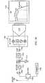
- FIG. 5is an illustration of a typical matching circuit 500 that can be used to implement embodiments of the disclosure.
- the matching circuitis operable to process input signals from a feed source 502 to provide load matching for an antenna 504.
- the embodiment shown in Figure 5comprises three reactive components (RC) RC a, RC b, and RC c, designated by reference numerals 506, 508, and 510, respectively.
- the reactive componentsmay be a combination of inductors or capacitors.
- the reactive componentshave a fixed value. However, in other embodiments, discussed below, the values of the reactive components may be variable.
- a load measurement P L ( f )is made. This step is repeated for two more measurements at the same measurement location by perturbing the frequency in ⁇ f steps to f + ⁇ f and f - ⁇ f .
- the corresponding load powers P L ( f + ⁇ f ) and P L ( f - ⁇ f )are then measured.
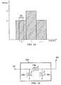
- Example power measurementsare shown generally in Figure 6 .
- two non-linear equations (5) and (6)(modifications of equations (2) and (3) above) are then constructed and solved for ⁇ A .
- the aforementioned power measurementsare the total received power.
- the power measurementsmay correspond to a desired user power component of the total received power.
- each of the three power measurements used in the aforementioned equationsmay be obtained by averaging power measurements at the various ⁇ f steps.
- Example 1An inverted F antenna (IFA) in voice usage mode.
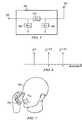
- Figure 7is a general illustration of a wireless handset 700 held adjacent to a user's head 702 (shown in phantom).
- the iterations to reach the solution of equations (2) and (3)are shown in Fig. 8 .
- the free-space input impedance 56+j11 Ohmsis used as the initial guess to the numerical solver.
- the exact impedance valuewas achieved.
- Fig. 9shows the error in the computed antenna impedance as a function of the perturbation bandwidth ⁇ f.
- Example 2Two dipole antennas near a phantom head.
- Figure 10is a general illustration of two dipole antennas 1002 and 1004 near a phantom head 1006.
- the initial antenna impedance guess assumedis 81+j65 ⁇ .
- the process for solving the system of equationsis shown in Fig. 11 .
- the actual complex input impedance of the antenna Z A64.4 +j63.4 ⁇ is successfully achieved.
- Fig. 12shows the error in the computed antenna impedance as a function of the perturbation bandwidth ⁇ f.
- Example 3Inverted F antenna used in "data mode.”
- Figure 13is a general illustration of a wireless device 1300 being held in a user's hands, illustrated generally by reference numeral 1302.
- the wireless device shown in Figure 13comprises a first antenna 1304 disposed on the lower edge of the device and a second antenna 1306 disposed on the left edge of the device.
- the antennas 1304 and 1306are oriented in an orthogonal configuration.
- the antennas 1304 and 1306can be inverted F antennas configured for use in a multiple-input-multiple-output (MIMO) system.
- MIMOmultiple-input-multiple-output
- the antennasoperate at a frequency of 2.5 GHz and the wireless device is operating in the presence of human hands as shown in Figure 13 .
- the input impedance of the antenna in free space60.27-j7.20 ⁇ ) is used as an initial guess.
- Figure 14is a graphical illustration of the solution process using the techniques described herein. This example shows that the approach described herein does not generate an incorrect value if there is no change measured in the antenna impedance from the previous computation.
- Figure 15is a graphical illustration of the error in the computed impedance as a function of the perturbation bandwidth for the calculations performed in Example 3.
- FIG. 17is an illustration of a communication system 1700 comprising functional components for processing signals in accordance with the techniques discussed herein.
- Antenna 1702is coupled to a duplexer 1704 that is further coupled to a transmitter 1706 and to a plurality of components comprising the receiver portion of the system.
- Incoming signalsare passed from the duplexer to a low noise amplifier (LNA) 1708 that generates amplified signal that are passed to a radio frequency (RF) filter 1710.
- LNAlow noise amplifier
- RF filter 1710is operable to filter the received signals and to provide a predetermined passband of the received RF signals to the mixer 1712.
- the mixer 1712mixes the RF signals with a lower frequency signal generated by a local oscillator to generate a set of intermediate frequency (IF) signals.
- the IF signalsare filtered by IF filter 1716 to generate a predetermined set of intermediate frequency signals that are then amplified by IF amplifier 1718 and passed to detector 1720 for further processing.
- the power sensing of the three needed power measurementsis performed at baseband.
- the ⁇ f perturbationsare accomplished by a shift in frequency using either local oscillator 1714 or local oscillator 1721.
- the response of the matching circuitshould be versatile in the range of 2 ⁇ f to ensure accurate power measurements. This can be accomplished by "mismatching" the fixed matching circuit by switching a component in or out of the circuit.
- the accuracy of the techniques described hereinimproves with the increase in the frequency step size ⁇ f.
- the examples discussed hereinshow that exact values of the impedance can be achieved with a ⁇ f of 15KHz. In some GSM applications, reasonable accuracy can be achieved with a ⁇ f of 10KHz and in some LTE applications, accurate impedance measurements may be possible with ⁇ f of 5KHz.
- the input impedance of an antennacan be obtained by using a combination of frequency perturbation and component perturbation techniques.
- FIG 18is an illustration of a tuning circuit 500a that is a modified version of the tuning circuit shown in Figure 5 .
- the reactive components 506a, 508a and 510aare variable, rather than having a fixed value.
- the received power measurementswill be expressed as "power parameters" corresponding to received power measurements made with frequency perturbations of the tuning circuit 500a and with the reactive components in the tuning circuit 500a having variable values.
- a first power parametercorresponds to a power measurement, P L 1 made at the operating frequency with the reactive component 508a set to a first predetermined value, C.
- the second power parametercorresponds to a power measurement, P L 2 , made at the operating frequency, f , but with the reactive component 508a set to a value of C+ ⁇ C.
- the third power parametercorresponds to a power measurement, P L 3 made with the reactive component 508a set to C+ ⁇ C, and with the frequency set either to f - ⁇ f or f + ⁇ f.
- equations (2) and (3)will be of the form shown below in equations (7) and (8):
- P L S C ⁇ 2 ⁇ ⁇ C ⁇ 2 P L SS 21 S C ⁇ 2 ⁇ ⁇ C ⁇ 2 2 ⁇ 1 - S 22 S ⁇ ⁇ L 2 ⁇ 1 - ⁇ A ⁇ ⁇ in S 2 S 21 S 2 ⁇ 1 - S 22 S C ⁇ 2 ⁇ ⁇ C ⁇ 2 ⁇ 1 - ⁇ A ⁇ ⁇ in S C ⁇ 2 ⁇ ⁇ C ⁇ 2 2 , and
- P L f ⁇ ⁇ f P L fS 21 f ⁇ ⁇ f 2 ⁇ 1 - S 22 S ⁇ ⁇ L 2 ⁇ 1 - ⁇ A ⁇ ⁇ in f 2 S 21 S 2 ⁇ 1 - S 22 f ⁇ ⁇ f ⁇ ⁇ L 2 ⁇ 1 - ⁇ A ⁇ ⁇ in f 2 .
- Figure 19is an illustration of a sequence of power measurements obtained using the relationships discussed above and the processing steps discussed previously in connection with other embodiments of the disclosure.
- the perturbation in frequencyis performed at digital baseband.
- the tuning of the equations' frequency componentis performed as the equivalent of the frequency perturbation discussed above, but is performed in DSP at digital baseband.
- the equations and analysesare the same as discussed hereinabove in connection with other embodiments.
- Figure 20is a block diagram representation of a system for implementing this embodiment. This system comprises all of the components discussed above in connection Figure 17 and also includes an analog-to-digital converter 1722 that converts analog baseband signals from the detector 1720 into digital signals that can be processed by the DSP 1724.
- This systemuses signal processing techniques known to those of skill in the art to perform frequency translation, Fast Fourier Transforming (FFT) and digital filtering.
- the DSP 1724can be configured to analyze incoming signals at frequencies offset from the received center of band, effectively performing frequency perturbations comparable to those discussed above with regard to other embodiments of the disclosure.
Landscapes
- Engineering & Computer Science (AREA)
- Computer Networks & Wireless Communication (AREA)
- Signal Processing (AREA)
- Mobile Radio Communication Systems (AREA)
Description
- The present disclosure is directed in general to communication systems and, more specifically, to systems and methods for real-time measurement of antenna impedance.
- The environment in which a wireless communication system is located can have a significant impact on the performance of antennas associated with the system. In particular, the power radiated by an antenna is affected by its proximity to objects, as, for example, a human, a metal object, a building, or a combination of such objects. To maximize the performance of a wireless communication system, it is important to compensate for environmental factors that may affect the efficiency of the antenna.
- It is especially advantageous to be able to determine the input impedance of the antenna in real time. For example, a change in the impedance may indicate a change in the channel that the wireless device is operating in. The change in the impedance information may be used to initiate a defined action. For example, in beam steering applications, the change in the antenna impedance value may indicate the need to initiate the beam steering process in search for a better link. In some applications, a known antenna input impedance value can be used to control tunable antenna components. Knowledge of the characteristics of the antenna impedance can also provide sense information regarding the near-field environment of the antenna (e.g., head, holster, etc.). Knowledge of the antenna input impedance in real-time can also be used to facilitate adaptive antenna impedance matching to compensate for the effects of the user.
- Aspects of an invention are set forth in the accompanying independent claims.
- The present invention may be understood, and its numerous objects, features and advantages obtained, when the following detailed description is considered in conjunction with the following drawings, in which:
Figure 1 depicts an exemplary system in which the present invention may be implemented;Figure 2 shows a wireless-enabled communications environment including an embodiment of a client node;Figure 3 is a simplified block diagram of an exemplary client node comprising a digital signal processor (DSP);Figure 4 is a simplified block diagram of a software environment that may be implemented by a DSP;Figure 5 is an illustration of a matching circuit that can be used to implement embodiments of the disclosure;Figure 6 is an illustration of example power measurements obtained using frequency perturbation techniques in accordance with an embodiment of the disclosure;Figure 7 is a general illustration of a wireless handset held adjacent to a user'shead 702;Figure 8 is a graphical representation of antenna input impedance for the example shown inFigure 7 ;Figure 9 shows the error in the computed antenna input impedance as a function of the perturbation bandwidth Δf for the example shown inFigure 7 ;Figure 10 is a general illustration of two dipole antennas near a user's head;Figure 11 is a graphical illustration of the computed antenna input impedance for the example shown inFigure 10 ;Figure 12 shows the error in the computed antenna input impedance as a function of the perturbation bandwidth Δf for the example shown inFigure 10 ;Figure 13 shows a communication device comprising an inverted-F antenna with the device being held in a user's hands;Figure 14 is a graphical representation of antenna input impedance for the example shown inFigure 13 ;Figure 15 is a graphical illustration of the error in the computed impedance as a function of the perturbation bandwidth for the calculations performed for the example shown inFigure 13 ;Figure 16 is an illustration of non-uniform signal power spectral density for communication systems implementing embodiments of the disclosure;Figure 17 is an illustration of a communication system comprising functional components for processing signals in accordance with embodiments of the disclosure;Figure 18 is an illustration of a tuning circuit that is a modified version of the tuning circuit shown inFigure 5 ;Figure 19 is an illustration of a sequence of power measurements obtained using the data processing techniques in accordance with embodiments of the disclosure; andFigure 20 is a block diagram representation of a system for implementing embodiments of the disclosure using digital signal processing techniques.- Embodiments of the disclosure provide systems and methods for real-time measurement of the input impedance of an antenna. In one embodiment, the input impedance of an antenna is measured by perturbing the frequency of operation of a matching circuit coupled to the antenna. In another embodiment, the input impedance is measured by perturbing the frequency of operation of the matching circuit and also perturbing the components of the matching circuit. In another embodiment, each of the aforementioned techniques is implemented by performing the equivalent of frequency perturbation in a digital signal processor operating at digital baseband.
- Various illustrative embodiments of the present invention will now be described in detail with reference to the accompanying figures. While various details are set forth in the following description, it will be appreciated that the present invention may be practiced without these specific details, and that numerous implementation-specific decisions may be made to the invention described herein to achieve the inventor's specific goals, such as compliance with process technology or design-related constraints, which will vary from one implementation to another. While such a development effort might be complex and time-consuming, it would nevertheless be a routine undertaking for those of skill in the art having the benefit of this disclosure. For example, selected aspects are shown in block diagram and flowchart form, rather than in detail, in order to avoid limiting or obscuring the present invention. In addition, some portions of the detailed descriptions provided herein are presented in terms of algorithms or operations on data within a computer memory. Such descriptions and representations are used by those skilled in the art to describe and convey the substance of their work to others skilled in the art.
- As used herein, the terms "component," "system" and the like are intended to refer to a computer-related entity, either hardware, software, a combination of hardware and software, or software in execution. For example, a component may be, but is not limited to being, a processor, a process running on a processor, an object, an executable, a thread of execution, a program, or a computer. By way of illustration, both an application running on a computer and the computer itself can be a component. One or more components may reside within a process or thread of execution and a component may be localized on one computer or distributed between two or more computers.
- As likewise used herein, the term "node" broadly refers to a connection point, such as a redistribution point or a communication endpoint, of a communication environment, such as a network. Accordingly, such nodes refer to an active electronic device capable of sending, receiving, or forwarding information over a communications channel. Examples of such nodes include data circuit-terminating equipment (DCE), such as a modem, hub, bridge or switch, and data terminal equipment (DTE), such as a handset, a printer or a host computer (e.g., a router, workstation or server). Examples of local area network (LAN) or wide area network
- (WAN) nodes include computers, packet switches, cable modems, Data Subscriber Line (DSL) modems, and wireless LAN (WLAN) access points. Examples of Internet or Intranet nodes include host computers identified by an Internet Protocol (IP) address, bridges and WLAN access points. Likewise, examples of nodes in cellular communication include base stations, relays, base station controllers, radio network controllers, home location registers, Gateway GPRS Support Nodes (GGSN), Serving GPRS Support Nodes (SGSN), Serving Gateways (S-GW), and Packet Data Network Gateways (PDN-GW).
- Other examples of nodes include client nodes, server nodes, peer nodes and access nodes. As used herein, a client node may refer to wireless devices such as mobile telephones, smart phones, personal digital assistants (PDAs), handheld devices, portable computers, tablet computers, and similar devices or other user equipment (UE) that has telecommunications capabilities. Such client nodes may likewise refer to a mobile, wireless device, or conversely, to devices that have similar capabilities that are not generally transportable, such as desktop computers, set-top boxes, or sensors. Likewise, a server node, as used herein, refers to an information processing device (e.g., a host computer), or series of information processing devices, that perform information processing requests submitted by other nodes. As likewise used herein, a peer node may sometimes serve as client node, and at other times, a server node. In a peer-to-peer or overlay network, a node that actively routes data for other networked devices as well as itself may be referred to as a supernode.
- An access node, as used herein, refers to a node that provides a client node access to a communication environment. Examples of access nodes include cellular network base stations and wireless broadband (e.g., WiFi, WiMAX, etc) access points, which provide corresponding cell and WLAN coverage areas. As used herein, a macrocell is used to generally describe a traditional cellular network cell coverage area. Such macrocells are typically found in rural areas, along highways, or in less populated areas. As likewise used herein, a microcell refers to a cellular network cell with a smaller coverage area than that of a macrocell. Such micro cells are typically used in a densely populated urban area. Likewise, as used herein, a picocell refers to a cellular network coverage area that is less than that of a microcell. An example of the coverage area of a picocell may be a large office, a shopping mall, or a train station. A femtocell, as used herein, currently refers to the smallest commonly accepted area of cellular network coverage. As an example, the coverage area of a femtocell is sufficient for homes or small offices.
- In general, a coverage area of less than two kilometers typically corresponds to a microcell, 200 meters or less for a picocell, and on the order of 10 meters for a femtocell. As likewise used herein, a client node communicating with an access node associated with a macrocell is referred to as a "macrocell client." Likewise, a client node communicating with an access node associated with a microcell, picocell, or femtocell is respectively referred to as a "microcell client," "picocell client," or "femtocell client."
- The term "article of manufacture" (or alternatively, "computer program product") as used herein is intended to encompass a computer program accessible from any computer-readable device or media. For example, computer readable media can include but are not limited to magnetic storage devices (e.g., hard disk, floppy disk, magnetic strips, etc.), optical disks such as a compact disk (CD) or digital versatile disk (DVD), smart cards, and flash memory devices (e.g., card, stick, etc.).
- The word "exemplary" is used herein to mean serving as an example, instance, or illustration. Any aspect or design described herein as "exemplary" is not necessarily to be construed as preferred or advantageous over other aspects or designs. Those of skill in the art will recognize many modifications may be made to this configuration without departing from the scope of the claimed subject matter. Furthermore, the disclosed subject matter may be implemented as a system, method, apparatus, or article of manufacture using standard programming and engineering techniques to produce software, firmware, hardware, or any combination thereof to control a computer or processor-based device to implement aspects detailed herein.
Figure 1 illustrates an example of asystem 100 suitable for implementing one or more embodiments disclosed herein. In various embodiments, thesystem 100 comprises aprocessor 110, which may be referred to as a central processor unit (CPU) or digital signal processor (DSP), network connectivity interfaces 120, random access memory (RAM) 130, read only memory (ROM) 140,secondary storage 150, and input/output (I/O)devices 160. In some embodiments, some of these components may not be present or may be combined in various combinations with one another or with other components not shown. These components may be located in a single physical entity or in more than one physical entity. Any actions described herein as being taken by theprocessor 110 might be taken by theprocessor 110 alone or by theprocessor 110 in conjunction with one or more components shown or not shown inFigure 1 .- The
processor 110 executes instructions, codes, computer programs, or scripts that it might access from the network connectivity interfaces 120,RAM 130, orROM 140. While only oneprocessor 110 is shown, multiple processors may be present. Thus, while instructions may be discussed as being executed by aprocessor 110, the instructions may be executed simultaneously, serially, or otherwise by one ormultiple processors 110 implemented as one or more CPU chips. - In various embodiments, the network connectivity interfaces 120 may take the form of modems, modem banks, Ethernet devices, universal serial bus (USB) interface devices, serial interfaces, token ring devices, fiber distributed data interface (FDDI) devices, wireless local area network (WLAN) devices, radio transceiver devices such as code division multiple access (CDMA) devices, global system for mobile communications (GSM) radio transceiver devices, long term evolution (LTE) radio transceiver devices, worldwide interoperability for microwave access (WiMAX) devices, and/or other well-known interfaces for connecting to networks, including Personal Area Networks (PANs) such as Bluetooth. These network connectivity interfaces 120 may enable the
processor 110 to communicate with the Internet or one or more telecommunications networks or other networks from which theprocessor 110 might receive information or to which theprocessor 110 might output information. - The network connectivity interfaces 120 may also be capable of transmitting or receiving data wirelessly in the form of electromagnetic waves, such as radio frequency signals or microwave frequency signals. Information transmitted or received by the network connectivity interfaces 120 may include data that has been processed by the
processor 110 or instructions that are to be executed byprocessor 110. The data may be ordered according to different sequences as may be desirable for either processing or generating the data or transmitting or receiving the data. - In various embodiments, the
RAM 130 may be used to store volatile data and instructions that are executed by theprocessor 110. TheROM 140 shown inFigure 1 may likewise be used to store instructions and data that are read during execution of the instructions. Thesecondary storage 150 is typically comprised of one or more disk drives or tape drives and may be used for non-volatile storage of data or as an overflow data storage device ifRAM 130 is not large enough to hold all working data.Secondary storage 150 may likewise be used to store programs that are loaded intoRAM 130 when such programs are selected for execution. The I/O devices 160 may include liquid crystal displays (LCDs), Light Emitting Diode (LED) displays, Organic Light Emitting Diode (OLED) displays, projectors, televisions, touch screen displays, keyboards, keypads, switches, dials, mice, track balls, voice recognizers, card readers, paper tape readers, printers, video monitors, or other well-known input/output devices. Figure 2 shows a wireless-enabled communications environment including an embodiment of a client node as implemented in an embodiment of the invention. Though illustrated as a mobile phone, theclient node 202 may take various forms including a wireless handset, a pager, a smart phone, or a personal digital assistant (PDA). In various embodiments, theclient node 202 may also comprise a portable computer, a tablet computer, a laptop computer, or any computing device operable to perform data communication operations. Many suitable devices combine some or all of these functions. In some embodiments, theclient node 202 is not a general purpose computing device like a portable, laptop, or tablet computer, but rather is a special-purpose communications device such as a telecommunications device installed in a vehicle. Theclient node 202 may likewise be a device, include a device, or be included in a device that has similar capabilities but that is not transportable, such as a desktop computer, a set-top box, or a network node. In these and other embodiments, theclient node 202 may support specialized activities such as gaming, inventory control, job control, task management functions, and so forth.- In various embodiments, the
client node 202 includes adisplay 204. In these and other embodiments, theclient node 202 may likewise include a touch-sensitive surface, a keyboard orother input keys 206 generally used for input by a user. Theinput keys 206 may likewise be a full or reduced alphanumeric keyboard such as QWERTY, Dvorak, AZERTY, and sequential keyboard types, or a traditional numeric keypad with alphabet letters associated with a telephone keypad. Theinput keys 206 may likewise include a trackwheel, an exit or escape key, a trackball, and other navigational or functional keys, which may be inwardly depressed to provide further input function. Theclient node 202 may likewise present options for the user to select, controls for the user to actuate, and cursors or other indicators for the user to direct. - The
client node 202 may further accept data entry from the user, including numbers to dial or various parameter values for configuring the operation of theclient node 202. Theclient node 202 may further execute one or more software or firmware applications in response to user commands. These applications may configure theclient node 202 to perform various customized functions in response to user interaction. Additionally, theclient node 202 may be programmed or configured over-the-air (OTA), for example from a wireless network access node 'A' 210 through 'n' 216 (e.g., a base station), a server node 224 (e.g., a host computer), or apeer client node 202. - Among the various applications executable by the
client node 202 are a web browser, which enables thedisplay 204 to display a web page. The web page may be obtained from aserver node 224 through a wireless connection with awireless network 220. As used herein, awireless network 220 broadly refers to any network using at least one wireless connection between two of its nodes. The various applications may likewise be obtained from apeer client node 202 or other system over a connection to thewireless network 220 or any other wirelessly-enabled communication network or system. - In various embodiments, the
wireless network 220 comprises a plurality of wireless sub-networks (e.g., cells with corresponding coverage areas) 'A' 212 through 'n' 218. As used herein, the wireless sub-networks 'A' 212 through 'n' 218 may variously comprise a mobile wireless access network or a fixed wireless access network. In these and other embodiments, theclient node 202 transmits and receives communication signals, which are respectively communicated to and from the wireless network nodes 'A' 210 through 'n' 216 by wireless network antennas 'A' 208 through 'n' 214 (e.g., cell towers). In turn, the communication signals are used by the wireless network access nodes 'A' 210 through 'n' 216 to establish a wireless communication session with theclient node 202. As used herein, the network access nodes 'A' 210 through 'n' 216 broadly refer to any access node of a wireless network. As shown inFigure 2 , the wireless network access nodes 'A' 210 through 'n' 216 are respectively coupled to wireless sub-networks 'A' 212 through 'n' 218, which are in turn connected to thewireless network 220. - In various embodiments, the
wireless network 220 is coupled to aphysical network 222, such as the Internet. Via thewireless network 220 and thephysical network 222, theclient node 202 has access to information on various hosts, such as theserver node 224. In these and other embodiments, theserver node 224 may provide content that may be shown on thedisplay 204 or used by theclient node processor 110 for its operations. Alternatively, theclient node 202 may access thewireless network 220 through apeer client node 202 acting as an intermediary, in a relay type or hop type of connection. As another alternative, theclient node 202 may be tethered and obtain its data from a linked device that is connected to thewireless network 212. Skilled practitioners of the art will recognize that many such embodiments are possible and the foregoing is not intended to limit the spirit, scope, or intention of the disclosure. Figure 3 depicts a block diagram of an exemplary client node as implemented with a digital signal processor (DSP) in accordance with an embodiment of the invention. While various components of aclient node 202 are depicted, various embodiments of theclient node 202 may include a subset of the listed components or additional components not listed. As shown inFigure 3 , theclient node 202 includes aDSP 302 and amemory 304. As shown, theclient node 202 may further include an antenna andfront end unit 306, a radio frequency (RF)transceiver 308, an analogbaseband processing unit 310, amicrophone 312, anearpiece speaker 314, aheadset port 316, abus 318, such as a system bus or an input/output (I/O) interface bus, aremovable memory card 320, a universal serial bus (USB)port 322, a short rangewireless communication sub-system 324, an alert 326, akeypad 328, a liquid crystal display (LCD) 330, which may include a touch sensitive surface, anLCD controller 332, a charge-coupled device (CCD)camera 334, acamera controller 336, and a global positioning system (GPS)sensor 338, and apower management module 340 operably coupled to a power storage unit, such as abattery 342. In various embodiments, theclient node 202 may include another kind of display that does not provide a touch sensitive screen. In one embodiment, theDSP 302 communicates directly with thememory 304 without passing through the input/output interface 318.- In various embodiments, the
DSP 302 or some other form of controller or central processing unit (CPU) operates to control the various components of theclient node 202 in accordance with embedded software or firmware stored inmemory 304 or stored in memory contained within theDSP 302 itself. In addition to the embedded software or firmware, theDSP 302 may execute other applications stored in thememory 304 or made available via information carrier media such as portable data storage media like theremovable memory card 320 or via wired or wireless network communications. The application software may comprise a compiled set of machine-readable instructions that configure theDSP 302 to provide the desired functionality, or the application software may be high-level software instructions to be processed by an interpreter or compiler to indirectly configure theDSP 302. - The antenna and
front end unit 306 may be provided to convert between wireless signals and electrical signals, enabling theclient node 202 to send and receive information from a cellular network or some other available wireless communications network or from apeer client node 202. In an embodiment, the antenna and front end unit 106 may include multiple antennas to support beam forming and/or multiple input multiple output (MIMO) operations. As is known to those skilled in the art, MIMO operations may provide spatial diversity which can be used to overcome difficult channel conditions or to increase channel throughput. Likewise, the antenna andfront end unit 306 may include antenna tuning or impedance matching components, RF power amplifiers, or low noise amplifiers. - In various embodiments, the
RF transceiver 308 provides frequency shifting, converting received RF signals to baseband and converting baseband transmit signals to RF. In some descriptions a radio transceiver or RF transceiver may be understood to include other signal processing functionality such as modulation/demodulation, coding/decoding, interleaving/deinterleaving, spreading/despreading, inverse fast Fourier transforming (IFFT)/fast Fourier transforming (FFT), cyclic prefix appending/removal, and other signal processing functions. For the purposes of clarity, the description here separates the description of this signal processing from the RF and/or radio stage and conceptually allocates that signal processing to the analogbaseband processing unit 310 or theDSP 302 or other central processing unit. In some embodiments, the RF Transceiver 108, portions of the Antenna andFront End 306, and the analog baseband processing unit 310 may be combined in one or more processing units and/or application specific integrated circuits (ASICs). - The analog
baseband processing unit 310 may provide various analog processing of inputs and outputs, for example analog processing of inputs from themicrophone 312 and theheadset 316 and outputs to theearpiece 314 and theheadset 316. To that end, the analogbaseband processing unit 310 may have ports for connecting to the built-inmicrophone 312 and theearpiece speaker 314 that enable theclient node 202 to be used as a cell phone. The analogbaseband processing unit 310 may further include a port for connecting to a headset or other hands-free microphone and speaker configuration. The analogbaseband processing unit 310 may provide digital-to-analog conversion in one signal direction and analog-to-digital conversion in the opposing signal direction. In various embodiments, at least some of the functionality of the analogbaseband processing unit 310 may be provided by digital processing components, for example by theDSP 302 or by other central processing units. - The
DSP 302 may perform modulation/demodulation, coding/decoding, interleaving/deinterleaving, spreading/despreading, inverse fast Fourier transforming (IFFT)/fast Fourier transforming (FFT), cyclic prefix appending/removal, and other signal processing functions associated with wireless communications. In an embodiment, for example in a code division multiple access (CDMA) technology application, for a transmitter function theDSP 302 may perform modulation, coding, interleaving, and spreading, and for a receiver function theDSP 302 may perform despreading, deinterleaving, decoding, and demodulation. In another embodiment, for example in an orthogonal frequency division multiplex access (OFDMA) technology application, for the transmitter function theDSP 302 may perform modulation, coding, interleaving, inverse fast Fourier transforming, and cyclic prefix appending, and for a receiver function theDSP 302 may perform cyclic prefix removal, fast Fourier transforming, deinterleaving, decoding, and demodulation. In other wireless technology applications, yet other signal processing functions and combinations of signal processing functions may be performed by theDSP 302. - The
DSP 302 may communicate with a wireless network via the analogbaseband processing unit 310. In some embodiments, the communication may provide Internet connectivity, enabling a user to gain access to content on the Internet and to send and receive e-mail or text messages. The input/output interface 318 interconnects theDSP 302 and various memories and interfaces. Thememory 304 and theremovable memory card 320 may provide software and data to configure the operation of theDSP 302. Among the interfaces may be theUSB interface 322 and the short rangewireless communication sub-system 324. TheUSB interface 322 may be used to charge theclient node 202 and may also enable theclient node 202 to function as a peripheral device to exchange information with a personal computer or other computer system. The short rangewireless communication sub-system 324 may include an infrared port, a Bluetooth interface, an IEEE 802.11 compliant wireless interface, or any other short range wireless communication sub-system, which may enable theclient node 202 to communicate wirelessly with other nearby client nodes and access nodes. - The input/
output interface 318 may further connect theDSP 302 to the alert 326 that, when triggered, causes theclient node 202 to provide a notice to the user, for example, by ringing, playing a melody, or vibrating. The alert 326 may serve as a mechanism for alerting the user to any of various events such as an incoming call, a new text message, and an appointment reminder by silently vibrating, or by playing a specific pre-assigned melody for a particular caller. - The
keypad 328 couples to theDSP 302 via the I/O interface 318 to provide one mechanism for the user to make selections, enter information, and otherwise provide input to theclient node 202. Thekeyboard 328 may be a full or reduced alphanumeric keyboard such as QWERTY, Dvorak, AZERTY and sequential types, or a traditional numeric keypad with alphabet letters associated with a telephone keypad. The input keys may likewise include a trackwheel, an exit or escape key, a trackball, and other navigational or functional keys, which may be inwardly depressed to provide further input function. Another input mechanism may be theLCD 330, which may include touch screen capability and also display text and/or graphics to the user. TheLCD controller 332 couples theDSP 302 to theLCD 330. - The
CCD camera 334, if equipped, enables theclient node 202 to take digital pictures. TheDSP 302 communicates with theCCD camera 334 via thecamera controller 336. In another embodiment, a camera operating according to a technology other than Charge Coupled Device cameras may be employed. TheGPS sensor 338 is coupled to theDSP 302 to decode global positioning system signals or other navigational signals, thereby enabling theclient node 202 to determine its position. Various other peripherals may also be included to provide additional functions, such as radio and television reception. Figure 4 illustrates asoftware environment 402 that may be implemented by a digital signal processor (DSP). In this embodiment, theDSP 302 shown inFigure 3 executes anoperating system 404, which provides a platform from which the rest of the software operates. Theoperating system 404 likewise provides theclient node 202 hardware with standardized interfaces (e.g., drivers) that are accessible to application software. Theoperating system 404 likewise comprises application management services (AMS) 406 that transfer control between applications running on theclient node 202. Also shown inFigure 4 are aweb browser application 408, amedia player application 410, andJava applets 412. Theweb browser application 408 configures theclient node 202 to operate as a web browser, allowing a user to enter information into forms and select links to retrieve and view web pages. Themedia player application 410 configures theclient node 202 to retrieve and play audio or audiovisual media. The Java applets 412 configure theclient node 202 to provide games, utilities, and other functionality. Acomponent 414 may provide functionality described herein. In various embodiments, theclient node 202, the wireless network nodes 'A' 210 through 'n' 216, and theserver node 224 shown inFigure 2 may likewise include a processing component that is capable of executing instructions related to the actions described above.- The present disclosure provides a tunable matching network in a radio frequency receiver system that matches, in real-time, the impedance of an antenna that may change dynamically because of various environmental factors. "Dynamic," as used in this disclosure, means adaptive or continuous changes responsive to a particular event or situation. In this application, "dynamic" refers to continuous changes in reaction to the environment or surroundings. The exact environmental variables that affect the antenna operation are not known or predictable. The impedance of an antenna may dynamically change as a result of a number of different factors, including, but not in any way limited to, antenna orientation and the proximity of the antenna to a number of bodies and objects, including inanimate objects.
- "Real-time," as used within this disclosure, refers to the continuous or ongoing processing of information without delay during the operation of hardware, software, or hardware and software. For example, a device or other hardware, software, or hardware/software combination is not considered to be operating in real-time when it is turned off, in a low power mode, a sleep mode, or a standby mode.
- The tunable matching network adapts the impedance of an antenna for a particular environment. Specifically, as the environment or the orientation of an antenna within an environment is changed, the input impedance of the antenna is calculated in real-time and the reactive elements of the matching network are calibrated continuously or dynamically to match the calculated input impedance of the antenna and tune the antenna to achieve optimal signal quality.
- The input impedance of the antenna is calculated in real-time through solving non-linear equations derived to determine the value of the reflection coefficient of the antenna, Gamma A,ΓA. Gamma A is a dynamic parameter of the antenna that changes with proximity to objects within a particular environment. The calculation of Gamma A in real-time allows the input impedance of the antenna to be determined dynamically. One or more reactive elements of the matching network may be adjusted to match the determined input impedance and maximize the power received from the antenna to the receiver system.
- A real-time impedance measurement technique was previously disclosed in U.S. Patent Application
US 2011/0086598 titled "Dynamic Real-Time Calibration for Antenna Matching in a Radio Frequency Receiver System." The technique disclosed in the above-referenced patent application was based on composing two non-linear equations based on three received power measurements, P1L, P2L, P3L. The received power measured at the terminal of the matching circuit that couples the antenna to a feed source is a function of the components that compose the matching circuit, i.e., inductors and capacitors, through the circuit's S-parameters, the operating frequencyf, and the antenna's input reflection coefficient. This relationship is shown below in equation 1:
- Using these three pieces of information, and utilizing equation (1), two non-linear equations (2) and (3) are composed and solved for the antenna input impedance,ΓA.

and
- The antenna input impedance,ΓA, can be obtained from the relationship shown below in equation (4):

where Zo is the characteristic impedance, usually of 50 ohms. Figure 5 is an illustration of atypical matching circuit 500 that can be used to implement embodiments of the disclosure. The matching circuit is operable to process input signals from afeed source 502 to provide load matching for anantenna 504. The embodiment shown inFigure 5 comprises three reactive components (RC) RC a, RC b, and RC c, designated byreference numerals Figure 5 , various embodiments of the disclosure can be implement using a different number of reactive components. In some embodiments of the disclosure the reactive components have a fixed value. However, in other embodiments, discussed below, the values of the reactive components may be variable.- At the operating frequency, f, a load measurement PL(f) is made. This step is repeated for two more measurements at the same measurement location by perturbing the frequency in Δf steps tof + Δf andf - Δf. The corresponding load powers PL(f+Δf) and PL(f-Δf) are then measured. Example power measurements are shown generally in
Figure 6 . Using the aforementioned information, two non-linear equations (5) and (6) (modifications of equations (2) and (3) above) are then constructed and solved forΓA.
and
- In some embodiments, the aforementioned power measurements are the total received power. In other embodiments, the power measurements may correspond to a desired user power component of the total received power. In addition, each of the three power measurements used in the aforementioned equations may be obtained by averaging power measurements at the various Δf steps.
- Three illustrative examples of the present disclosure for implementing the techniques discussed above will now be discussed:
- Example 1: An inverted F antenna (IFA) in voice usage mode.
Figure 7 is a general illustration of awireless handset 700 held adjacent to a user's head 702 (shown in phantom). In this example, a frequency of f= 2.6 GHz is used. Equations (2)-(4) are solved with the measured received powers at Δf=100MHz perturbations in frequency. The iterations to reach the solution of equations (2) and (3) are shown inFig. 8 . The actual input impedance of the antenna is successfully recovered to be ZA=67+j0.4 Ohms. The free-space input impedance 56+j11 Ohms is used as the initial guess to the numerical solver. - For practical implementation, Δf needs to be such that all three measurements occur in one communication interval. Therefore, the same example is calculated with Δf=10KHz, which would work with the bandwidth for GSM applications. The solution of the two equations yielded an impedance value of ZA=57.7+j20.6 Ω. When repeated with an LTE application in mind for Δf=5MHz (and assuming an LTE carrier bandwidth of 20MHz), the exact impedance value was achieved.
Fig. 9 shows the error in the computed antenna impedance as a function of the perturbation bandwidth Δf. - Example 2: Two dipole antennas near a phantom head.
Figure 10 is a general illustration of twodipole antennas phantom head 1006. In this example, two dipole antennas operating at a frequency of 1.88 GHz are considered. The initial antenna impedance guess assumed is 81+j65Ω. The perturbations in frequency are made in Δf=100MHz steps. The process for solving the system of equations is shown inFig. 11 . The actual complex input impedance of the antenna ZA= 64.4 +j63.4 Ω is successfully achieved. - The same example was run with Δf=10KHz for consideration of GSM applications. The solution of the two equations came to the approximate impedance value of ZA=77.1+j61.4 Ω. When repeated with an LTE application in mind for Δf=5MHz, the exact impedance value was achieved.
Fig. 12 shows the error in the computed antenna impedance as a function of the perturbation bandwidth Δf. - Example 3: Inverted F antenna used in "data mode."
Figure 13 is a general illustration of awireless device 1300 being held in a user's hands, illustrated generally byreference numeral 1302. The wireless device shown inFigure 13 comprises afirst antenna 1304 disposed on the lower edge of the device and asecond antenna 1306 disposed on the left edge of the device. As will be understood by those of skill in the art, theantennas antennas - In this example, it is assumed that the antennas operate at a frequency of 2.5 GHz and the wireless device is operating in the presence of human hands as shown in
Figure 13 . In this example the actual input impedance of the antenna is calculated to be ZA=60.69-j6.3 Ω. The input impedance of the antenna in free space (60.27-j7.20 Ω) is used as an initial guess. Figure 14 is a graphical illustration of the solution process using the techniques described herein. This example shows that the approach described herein does not generate an incorrect value if there is no change measured in the antenna impedance from the previous computation.Figure 15 is a graphical illustration of the error in the computed impedance as a function of the perturbation bandwidth for the calculations performed in Example 3.- The previous analysis is based on the assumption that the received power observed at the base of the antenna being the same at frequenciesf-Δf, f, andf+Δf. Assuming a fixed impedance value, if there is a natural change in the received power change at these three frequencies then power measurements used in equations (2) and (3) must be normalized for an accurate comparison. The basis for this normalization can be seen be referring to the spectral density illustration in
Figure 16 . As shown, power measurements in the region off are made on a portion of the signal that has a power spectral density L2-L1 dB greater than for measurements in made in the regionsf-Δf orf+Δf. Therefore, to properly compare power measurements of P1/P3 centered onf-Δf /f+Δf with measurements of P2 centered onf, the measurements of P2 must be adjusted by L2-L1 dB. Figure 17 is an illustration of acommunication system 1700 comprising functional components for processing signals in accordance with the techniques discussed herein.Antenna 1702 is coupled to aduplexer 1704 that is further coupled to atransmitter 1706 and to a plurality of components comprising the receiver portion of the system. Incoming signals are passed from the duplexer to a low noise amplifier (LNA) 1708 that generates amplified signal that are passed to a radio frequency (RF)filter 1710. TheRF filter 1710 is operable to filter the received signals and to provide a predetermined passband of the received RF signals to themixer 1712. Themixer 1712 mixes the RF signals with a lower frequency signal generated by a local oscillator to generate a set of intermediate frequency (IF) signals. The IF signals are filtered byIF filter 1716 to generate a predetermined set of intermediate frequency signals that are then amplified byIF amplifier 1718 and passed todetector 1720 for further processing.- In one embodiments of the invention, the power sensing of the three needed power measurements is performed at baseband. The Δf perturbations are accomplished by a shift in frequency using either
local oscillator 1714 orlocal oscillator 1721. - In the implementation of the various embodiments, the response of the matching circuit should be versatile in the range of 2Δf to ensure accurate power measurements. This can be accomplished by "mismatching" the fixed matching circuit by switching a component in or out of the circuit. As can be understood from
Figures 9 ,12 and15 , the accuracy of the techniques described herein improves with the increase in the frequency step size Δf. The examples discussed herein show that exact values of the impedance can be achieved with a Δf of 15KHz. In some GSM applications, reasonable accuracy can be achieved with a Δf of 10KHz and in some LTE applications, accurate impedance measurements may be possible with Δf of 5KHz. - In the embodiments discussed hereinabove, all of the impedance measurements have been accomplished by using only frequency perturbations. In an alternate embodiment of the disclosure, the input impedance of an antenna can be obtained by using a combination of frequency perturbation and component perturbation techniques.
Figure 18 is an illustration of atuning circuit 500a that is a modified version of the tuning circuit shown inFigure 5 . In the tuning circuit shown inFigure 18 , thereactive components tuning circuit 500a and with the reactive components in thetuning circuit 500a having variable values.- Although implementation of this embodiment may be accomplished by varying the values of any of the reactive components, or any combination of the reactive components, examples will be discussed wherein
reactive component 508a is a capacitor having a capacitance, C, and the value of the reactive element is varied by an amount, ΔC. In this example a first power parameter corresponds to a power measurement, PL1 made at the operating frequency with thereactive component 508a set to a first predetermined value, C. The second power parameter corresponds to a power measurement, PL2, made at the operating frequency,f, but with thereactive component 508a set to a value of C+ΔC. The third power parameter corresponds to a power measurement, PL3 made with thereactive component 508a set to C+ΔC, and with the frequency set either tof-Δf orf+Δf. - Using this technique, equations (2) and (3) will be of the form shown below in equations (7) and (8):

and
Figure 19 is an illustration of a sequence of power measurements obtained using the relationships discussed above and the processing steps discussed previously in connection with other embodiments of the disclosure.- In yet another embodiment, the perturbation in frequency is performed at digital baseband. This embodiment, the tuning of the equations' frequency component is performed as the equivalent of the frequency perturbation discussed above, but is performed in DSP at digital baseband. The equations and analyses are the same as discussed hereinabove in connection with other embodiments.
Figure 20 is a block diagram representation of a system for implementing this embodiment. This system comprises all of the components discussed above in connectionFigure 17 and also includes an analog-to-digital converter 1722 that converts analog baseband signals from thedetector 1720 into digital signals that can be processed by theDSP 1724. This system uses signal processing techniques known to those of skill in the art to perform frequency translation, Fast Fourier Transforming (FFT) and digital filtering. TheDSP 1724 can be configured to analyze incoming signals at frequencies offset from the received center of band, effectively performing frequency perturbations comparable to those discussed above with regard to other embodiments of the disclosure. - Although the described exemplary embodiments disclosed herein are described with reference to estimating the impedance of antennas in wireless devices, the present disclosure is not necessarily limited to the example embodiments which illustrate inventive aspects of the present invention that are applicable to a wide variety of authentication algorithms. Thus, the particular embodiments disclosed above are illustrative only and should not be taken as limitations upon the present invention, as the invention may be modified and practiced in different but equivalent manners apparent to those skilled in the art having the benefit of the teachings herein. Accordingly, the foregoing description is not intended to limit the invention to the particular form set forth, but on the contrary, is intended to cover such alternatives, modifications and equivalents as may be included within the scope of the invention as defined by the appended claims so that those skilled in the art should understand that they can make various changes, substitutions and alterations without departing from the spirit and scope of the invention in its broadest form.


Claims (15)
- A wireless communications system (100), comprising:an antenna (504);a matching circuit (500) coupled to said antenna (504), said matching circuit (500) having an operating frequency;a control system operable to calculate, in real-time, a value for an input impedance of the antenna (504), wherein said input impedance is calculated based on a first received power measurement corresponding to said matching circuit (500) tuned at said operating frequency, a second received power measurement corresponding to said matching circuit (500) tuned at a first perturbed frequency equal to the operating frequency minus a frequency perturbation step interval, and a third received power measurement corresponding to said matching circuit (500) tuned at a second perturbed frequency equal to the operating frequency plus the frequency perturbation step interval.
- The wireless communications system (100) of claim 1, wherein said first, second, and third received power measurements, respectively, each comprise the total received power.
- The wireless communications system (100) of claim 1, wherein said first, second, and third received power measurements, respectively, each correspond to a desired user power.
- The wireless communications system (100) of any of claims 1 to 3, wherein one of said first, second, and third received power measurements is obtained by averaging a collective set of power measurements.
- The wireless communications system (100) of any of claims 1 to 4, wherein said matching network (500) is tunable by the control system to match the calculated values of the input impedance of the antenna to a load on a receiver in said communication system.
- The wireless communications system (100) of any of claims 1 to 5, wherein said matching network (500) comprises reactive components having fixed values.
- The wireless communications system (100) of claim 6, wherein said first, second, and third received power measurements are normalized to compensate for received power variations corresponding to spectral power densities for the measurement frequencies for each of the three respective power measurements.
- The wireless communications system (100) of any of claims 1 to 7, wherein said frequency perturbation step interval is implemented by controlling the frequency generated by a local oscillator in a detector of a receiver, prior to the baseband stage, in said communication system.
- The wireless communications system (100) of claim 8, wherein the power sensing of said first, second, and third received power measurements, respectively, is performed at the baseband frequency of the receiver in said communication system.
- A method for processing signals received on a wireless communications system (100), the method comprising:receiving a signal on an antenna (504) coupled to said wireless communication system;providing said received signal to a matching circuit (500) coupled to said antenna (504), said matching circuit having an operating frequency; andusing a control system operable to calculate, in real-time, a value for an input impedance of the antenna (504) to match a load in a receiver system, wherein said input impedance is calculated based on a first received power measurement corresponding to said matching circuit (500) tuned at said operating frequency, and a second received power measurement corresponding to said matching circuit (500) tuned at a first perturbed frequency equal to the operating frequency minus a frequency perturbation step interval, and a third received power measurement corresponding to said matching circuit tuned at a second perturbed frequency equal to the operating frequency plus the frequency perturbation step interval.
- The method of claim 10, wherein said matching network (500) is tunable by the control system to match the calculated values of the input impedance of the antenna to a load on a receiver in said communication system.
- The method of claim 10 or claim 11, wherein said matching network (500) comprises reactive components having fixed values.
- The method of claim 12, wherein said first, second, and third received power measurements are normalized to compensate for received power variations corresponding to spectral power densities for the measurement frequencies for each of the three respective power measurements.
- The method of any of claims 10 to 13, wherein said frequency perturbation step interval is implemented by controlling the frequency generated by a local oscillator in a detector of a receiver, prior to the baseband stage, in said communication system (100); and optionally
wherein the power sensing of said first, second, and third received power measurements, respectively, is performed at the baseband frequency of the receiver in said communication system. - A computer-readable medium comprising computer-readable instructions which, when executed by a processor, cause the processor to perform the method of any of claims 10 to 14.
Applications Claiming Priority (1)
| Application Number | Priority Date | Filing Date | Title |
|---|---|---|---|
| PCT/US2011/060540WO2013074063A1 (en) | 2011-11-14 | 2011-11-14 | Perturbation-based dynamic measurement of antenna impedance in real-time |
Publications (2)
| Publication Number | Publication Date |
|---|---|
| EP2781030A1 EP2781030A1 (en) | 2014-09-24 |
| EP2781030B1true EP2781030B1 (en) | 2015-10-21 |
Family
ID=45099182
Family Applications (1)
| Application Number | Title | Priority Date | Filing Date |
|---|---|---|---|
| EP11791686.6AActiveEP2781030B1 (en) | 2011-11-14 | 2011-11-14 | Perturbation-based dynamic measurement of antenna impedance in real-time |
Country Status (3)
| Country | Link |
|---|---|
| US (1) | US9331723B2 (en) |
| EP (1) | EP2781030B1 (en) |
| WO (1) | WO2013074063A1 (en) |
Families Citing this family (22)
| Publication number | Priority date | Publication date | Assignee | Title |
|---|---|---|---|---|
| US8744384B2 (en) | 2000-07-20 | 2014-06-03 | Blackberry Limited | Tunable microwave devices with auto-adjusting matching circuit |
| US7711337B2 (en) | 2006-01-14 | 2010-05-04 | Paratek Microwave, Inc. | Adaptive impedance matching module (AIMM) control architectures |
| US7714676B2 (en) | 2006-11-08 | 2010-05-11 | Paratek Microwave, Inc. | Adaptive impedance matching apparatus, system and method |
| US7535312B2 (en) | 2006-11-08 | 2009-05-19 | Paratek Microwave, Inc. | Adaptive impedance matching apparatus, system and method with improved dynamic range |
| US7991363B2 (en) | 2007-11-14 | 2011-08-02 | Paratek Microwave, Inc. | Tuning matching circuits for transmitter and receiver bands as a function of transmitter metrics |
| US9026062B2 (en) | 2009-10-10 | 2015-05-05 | Blackberry Limited | Method and apparatus for managing operations of a communication device |
| US8803631B2 (en) | 2010-03-22 | 2014-08-12 | Blackberry Limited | Method and apparatus for adapting a variable impedance network |
| JP5901612B2 (en) | 2010-04-20 | 2016-04-13 | ブラックベリー リミテッド | Method and apparatus for managing interference in a communication device |
| US9379454B2 (en) | 2010-11-08 | 2016-06-28 | Blackberry Limited | Method and apparatus for tuning antennas in a communication device |
| US8712340B2 (en) | 2011-02-18 | 2014-04-29 | Blackberry Limited | Method and apparatus for radio antenna frequency tuning |
| US8594584B2 (en) | 2011-05-16 | 2013-11-26 | Blackberry Limited | Method and apparatus for tuning a communication device |
| GB2492775B (en)* | 2011-07-11 | 2013-08-28 | Cambridge Silicon Radio Ltd | Near field communications apparatus |
| EP2740221B1 (en) | 2011-08-05 | 2019-06-26 | BlackBerry Limited | Method and apparatus for band tuning in a communication device |
| US8948889B2 (en) | 2012-06-01 | 2015-02-03 | Blackberry Limited | Methods and apparatus for tuning circuit components of a communication device |
| US9350405B2 (en) | 2012-07-19 | 2016-05-24 | Blackberry Limited | Method and apparatus for antenna tuning and power consumption management in a communication device |
| US9374113B2 (en) | 2012-12-21 | 2016-06-21 | Blackberry Limited | Method and apparatus for adjusting the timing of radio antenna tuning |
| US10404295B2 (en) | 2012-12-21 | 2019-09-03 | Blackberry Limited | Method and apparatus for adjusting the timing of radio antenna tuning |
| US9467104B2 (en)* | 2014-03-28 | 2016-10-11 | Qualcomm Incorporated | Single-input multiple-output amplifiers with simultaneous multiple gain modes |
| US9438319B2 (en) | 2014-12-16 | 2016-09-06 | Blackberry Limited | Method and apparatus for antenna selection |
| US20200104678A1 (en)* | 2018-09-27 | 2020-04-02 | Google Llc | Training optimizer neural networks |
| US12143132B2 (en) | 2021-03-18 | 2024-11-12 | Skyworks Solutions, Inc. | Power amplifier systems with non-linear antenna impedance for load compensation |
| CN120110408B (en)* | 2025-05-08 | 2025-08-12 | 北京中讯四方科技股份有限公司 | Self-adaptive impedance matching method and system for microwave frequency band |
Family Cites Families (72)
| Publication number | Priority date | Publication date | Assignee | Title |
|---|---|---|---|---|
| US3366883A (en) | 1965-12-20 | 1968-01-30 | Avco Corp | Automatic broad band vswr power control |
| US3590385A (en) | 1969-07-25 | 1971-06-29 | Avco Corp | Semi-automatic tuning circuit for an antenna coupler |
| US3794941A (en)* | 1972-05-08 | 1974-02-26 | Hughes Aircraft Co | Automatic antenna impedance tuner including digital control circuits |
| US4165493A (en) | 1978-04-17 | 1979-08-21 | Rockwell International Corporation | Protected amplifier apparatus |
| FR2573940B1 (en) | 1984-11-23 | 1987-06-12 | Thomson Csf | DEVICE FOR AUTOMATIC ADJUSTMENT OF THE ADAPTATION CELL OF AN ANTENNA ON ITS WORKING FREQUENCY |
| US4739329A (en) | 1986-04-16 | 1988-04-19 | Motorola, Inc. | Scaler scoring system |
| US5564086A (en) | 1993-11-29 | 1996-10-08 | Motorola, Inc. | Method and apparatus for enhancing an operating characteristic of a radio transmitter |
| US6414562B1 (en) | 1997-05-27 | 2002-07-02 | Motorola, Inc. | Circuit and method for impedance matching |
| US5991282A (en) | 1997-05-28 | 1999-11-23 | Telefonaktiebolaget Lm Ericsson | Radio communication system with diversity reception on a time-slot by time-slot basis |
| US6301693B1 (en) | 1998-12-16 | 2001-10-09 | Synopsys, Inc. | Non-linear optimization system and method for wire length and delay optimization for an automatic electric circuit placer |
| US6356744B1 (en) | 1999-01-07 | 2002-03-12 | Uniden America Corporation | Power measurement circuit |
| US6757423B1 (en) | 1999-02-19 | 2004-06-29 | Barnes-Jewish Hospital | Methods of processing tagged MRI data indicative of tissue motion including 4-D LV tissue tracking |
| FI990687L (en) | 1999-03-29 | 2000-09-30 | Nokia Mobile Phones Ltd | Wireless communication antenna matching system |
| US6804262B1 (en) | 2000-04-28 | 2004-10-12 | 3Com Corporation | Method and apparatus for channel determination through power measurements |
| US6262684B1 (en) | 2000-06-27 | 2001-07-17 | 3Com Corporation | Stylus antenna |
| US6326922B1 (en) | 2000-06-29 | 2001-12-04 | Worldspace Corporation | Yagi antenna coupled with a low noise amplifier on the same printed circuit board |
| US7865154B2 (en) | 2000-07-20 | 2011-01-04 | Paratek Microwave, Inc. | Tunable microwave devices with auto-adjusting matching circuit |
| US20030048223A1 (en) | 2000-11-07 | 2003-03-13 | Vytas Kezys | Content-based adaptive parasitic array antenna system |
| US7071776B2 (en) | 2001-10-22 | 2006-07-04 | Kyocera Wireless Corp. | Systems and methods for controlling output power in a communication device |
| US6946847B2 (en) | 2002-02-08 | 2005-09-20 | Daihen Corporation | Impedance matching device provided with reactance-impedance table |
| US6993297B2 (en) | 2002-07-12 | 2006-01-31 | Sony Ericsson Mobile Communications Ab | Apparatus and methods for tuning antenna impedance using transmitter and receiver parameters |
| DE10233123A1 (en) | 2002-07-20 | 2004-02-05 | Philips Intellectual Property & Standards Gmbh | Device for dynamically adjusting the impedance between a power amplifier and an antenna |
| EP1542311A4 (en) | 2002-11-01 | 2011-01-05 | Fujitsu Ltd | DEVICE AND METHOD FOR CONTROLLING |
| JP3931163B2 (en) | 2003-08-14 | 2007-06-13 | 松下電器産業株式会社 | Antenna matching device |
| US7379714B2 (en) | 2004-04-02 | 2008-05-27 | Interdigital Technology Corporation | Method and apparatus for dynamically adjusting a transmitter's impedance |
| ATE470271T1 (en) | 2004-09-09 | 2010-06-15 | Epcos Ag | IMPROVEMENTS IN OR RELATING TO ANTENNA MATCHING IN VIDEO RECEIVER |
| US7426373B2 (en)* | 2005-01-11 | 2008-09-16 | The Boeing Company | Electrically tuned resonance circuit using piezo and magnetostrictive materials |
| US7528674B2 (en) | 2005-01-31 | 2009-05-05 | Panasonic Corporation | Mobile radio apparatus capable of adaptive impedance matching |
| US7376407B2 (en) | 2005-04-28 | 2008-05-20 | Microtune (Texas), L.P. | System and method for dynamic impedance tuning to minimize return loss |
| US7586384B2 (en) | 2005-08-15 | 2009-09-08 | Nokia Corporation | Integrated load impedance sensing for tunable matching networks |
| US7756486B1 (en) | 2005-11-16 | 2010-07-13 | Marvell International Ltd. | Transmitter and receiver impedance control using shunt switches |
| DE102005058875B4 (en) | 2005-12-09 | 2016-02-25 | Infineon Technologies Ag | matching |
| KR100752280B1 (en) | 2005-12-14 | 2007-08-28 | 삼성전자주식회사 | Device for matching frequency of antenna automatically in wireless terminal |
| US7711337B2 (en) | 2006-01-14 | 2010-05-04 | Paratek Microwave, Inc. | Adaptive impedance matching module (AIMM) control architectures |
| US7650263B2 (en) | 2006-09-26 | 2010-01-19 | Strider Labs, Inc. | Method for fast computation of optimal contact forces |
| US7877070B2 (en) | 2006-09-29 | 2011-01-25 | Broadcom Corp. | Method and system for tuning an antenna using injection |
| US7409245B1 (en) | 2007-01-30 | 2008-08-05 | Cardiac Pacemakers, Inc. | Variable antenna matching network for an implantable antenna |
| US7746291B2 (en) | 2007-01-30 | 2010-06-29 | Broadcom Corporation | RF reception system and integrated circuit with programmable impedance matching network and methods for use therewith |
| US20080233869A1 (en) | 2007-03-19 | 2008-09-25 | Thomas Baker | Method and system for a single-chip fm tuning system for transmit and receive antennas |
| US20100069011A1 (en) | 2007-04-19 | 2010-03-18 | Thingmagic, Inc. | Methods and Apparatus For Self-Jamming Suppression In A Radio Frequency Identification (RFID) Reader |
| US7917104B2 (en) | 2007-04-23 | 2011-03-29 | Paratek Microwave, Inc. | Techniques for improved adaptive impedance matching |
| US8213886B2 (en) | 2007-05-07 | 2012-07-03 | Paratek Microwave, Inc. | Hybrid techniques for antenna retuning utilizing transmit and receive power information |
| US7764942B2 (en) | 2007-07-06 | 2010-07-27 | Anadigics, Inc. | Tuning circuitry utilizing frequency translation of an impedance from a fixed-filter frequency response |
| FR2920927B1 (en) | 2007-09-11 | 2011-05-06 | Commissariat Energie Atomique | AUTOMATIC RADIOFREQUENCY CIRCUIT IMPEDANCE ADAPTATION METHOD AND AUTOMATICALLY ADAPTABLE TRANSMISSION OR RECEPTION SYSTEM |
| US7991363B2 (en) | 2007-11-14 | 2011-08-02 | Paratek Microwave, Inc. | Tuning matching circuits for transmitter and receiver bands as a function of transmitter metrics |
| US7933574B2 (en) | 2007-11-16 | 2011-04-26 | Broadcom Corporation | Method and system for LNA adjustment to compensate for dynamic impedance matching |
| US20090157334A1 (en) | 2007-12-14 | 2009-06-18 | Kenneth Joseph Goodnow | Measurement of power consumption within an integrated circuit |
| JP4962298B2 (en) | 2007-12-19 | 2012-06-27 | 富士通株式会社 | Transceiver |
| TWI355500B (en) | 2008-01-10 | 2012-01-01 | Wistron Neweb Corp | Test system for adjusting a wireless communication |
| US8330667B2 (en) | 2008-01-14 | 2012-12-11 | Epcos Ag | Portable wireless device |
| US7839223B2 (en)* | 2008-03-23 | 2010-11-23 | Advanced Energy Industries, Inc. | Method and apparatus for advanced frequency tuning |
| US20090267746A1 (en) | 2008-04-23 | 2009-10-29 | Martec Corporation | Multi-Port Receiver |
| US20090267703A1 (en)* | 2008-04-23 | 2009-10-29 | Andrzej May | Dynamically adaptable impedance matching circuitry between an electro-optical load and a driving source |
| EP2151921B1 (en) | 2008-08-07 | 2013-10-02 | Epcos AG | Dynamic impedance matching network and method for matching an impedance between a source and a load |
| US8072285B2 (en) | 2008-09-24 | 2011-12-06 | Paratek Microwave, Inc. | Methods for tuning an adaptive impedance matching network with a look-up table |
| US8270921B2 (en)* | 2009-04-27 | 2012-09-18 | Csr Technology Inc. | Systems and methods for tuning an antenna for a frequency modulation transceiver |
| US8948713B2 (en) | 2009-06-16 | 2015-02-03 | Broadcom Corporation | Antenna impedance/power amplifier source impedance measurement circuitry and device operation based thereon |
| FR2949922B1 (en)* | 2009-09-07 | 2011-10-28 | Commissariat Energie Atomique | MULTIBAND ANTENNA IMPEDANCE ADAPTATION METHOD AND AUTOMATICALLY ADAPTABLE TRANSMISSION OR RECEPTION CHAIN. |
| US9250328B2 (en) | 2009-09-30 | 2016-02-02 | Javad Gnss, Inc. | Graphics-aided remote position measurement with handheld geodesic device |
| US8131232B2 (en) | 2009-10-09 | 2012-03-06 | Texas Instruments Incorporated | Method and apparatus for antenna tuning |
| US8774743B2 (en)* | 2009-10-14 | 2014-07-08 | Blackberry Limited | Dynamic real-time calibration for antenna matching in a radio frequency receiver system |
| US8190109B2 (en)* | 2009-10-14 | 2012-05-29 | Research In Motion Limited | Dynamic real-time calibration for antenna matching in a radio frequency transmitter system |
| US8326234B2 (en) | 2010-02-12 | 2012-12-04 | Infineon Technologies Ag | High frequency switching circuit and method for determining a power of a high frequency signal |
| JP5901612B2 (en) | 2010-04-20 | 2016-04-13 | ブラックベリー リミテッド | Method and apparatus for managing interference in a communication device |
| US8310309B2 (en) | 2010-05-03 | 2012-11-13 | Qualcomm, Incorporated | Noise-canceling for differential amplifiers requiring no external matching |
| EP2609686B1 (en)* | 2010-08-26 | 2019-10-09 | Wispry, Inc. | Tunable radio front end and methods |
| US8712348B2 (en) | 2010-09-01 | 2014-04-29 | Samsung Electronics Co., Ltd. | Apparatus and method for controlling a tunable matching network in a wireless network |
| DE102010047440A1 (en)* | 2010-10-04 | 2012-04-05 | Epcos Ag | Device for wireless information transmission, communication terminal for wireless information transmission and method for impedance matching |
| WO2012067622A1 (en) | 2010-11-19 | 2012-05-24 | Research In Motion Limited | Dynamic real-time calibration for antenna matching in a radio frequency receiver system |
| US20120217817A1 (en)* | 2011-02-28 | 2012-08-30 | Bingnan Wang | Tuning Electromagnetic Fields Characteristics for Wireless Energy Transfer Using Arrays of Resonant Objects |
| TWI446761B (en)* | 2011-04-01 | 2014-07-21 | Htc Corp | Method of dynamic impedance matching and communication apparatus therewith |
| FR2973968B1 (en) | 2011-04-07 | 2013-04-12 | Commissariat Energie Atomique | RADIOFREQUENCY TRANSMITTING OR RECEPTION CHAIN WITH AUTOMATIC IMPEDANCE ADAPTATION AND CORRESPONDING METHOD |
- 2011
- 2011-11-14USUS14/357,404patent/US9331723B2/enactiveActive
- 2011-11-14EPEP11791686.6Apatent/EP2781030B1/enactiveActive
- 2011-11-14WOPCT/US2011/060540patent/WO2013074063A1/enactiveApplication Filing
Also Published As
| Publication number | Publication date |
|---|---|
| EP2781030A1 (en) | 2014-09-24 |
| WO2013074063A1 (en) | 2013-05-23 |
| US9331723B2 (en) | 2016-05-03 |
| US20140287698A1 (en) | 2014-09-25 |
Similar Documents
| Publication | Publication Date | Title |
|---|---|---|
| EP2781030B1 (en) | Perturbation-based dynamic measurement of antenna impedance in real-time | |
| US9083074B2 (en) | Dynamic antenna selection based on user hand position | |
| US9722324B2 (en) | Method and apparatus to control mutual coupling and correlation for multi-antenna applications | |
| US9225058B2 (en) | Flex PCB folded antenna | |
| US20140119244A1 (en) | Cognitive radio rf front end | |
| EP2650969B1 (en) | Compact broadband antenna | |
| US9264124B2 (en) | Antenna polarization optimization for wireless communications | |
| US9331381B2 (en) | Method and apparatus for tunable antenna and ground plane for handset applications | |
| US20130265889A1 (en) | Optimized Uplink Performance via Antenna Selection | |
| EP2797240B1 (en) | Antenna polarization optimization for wireless communications | |
| CN109565291A (en) | It is tuned by the centre frequency and Q of the biquadratic filter of the calibration based on amplitude limiting oscillation | |
| EP2860821A1 (en) | Millimeter-wave broadband transition of microstrip line on thin to thick substrates | |
| EP3276840A1 (en) | Method and apparatus for dynamic tuning | |
| EP3276841A1 (en) | Method and apparatus for dynamic tuning | |
| US9653779B2 (en) | Dual-band LTE MIMO antenna | |
| EP2728760B1 (en) | Adaptive antenna matching via a transceiver-based perturbation technique | |
| EP2797168A1 (en) | Monopole antenna with a tapered balun | |
| US9634395B2 (en) | Monopole antenna with a tapered Balun | |
| US9728848B1 (en) | Adaptive neutralization line to counter environmental effects for ultra-high isolation |
Legal Events
| Date | Code | Title | Description |
|---|---|---|---|
| PUAI | Public reference made under article 153(3) epc to a published international application that has entered the european phase | Free format text:ORIGINAL CODE: 0009012 | |
| 17P | Request for examination filed | Effective date:20140610 | |
| AK | Designated contracting states | Kind code of ref document:A1 Designated state(s):AL AT BE BG CH CY CZ DE DK EE ES FI FR GB GR HR HU IE IS IT LI LT LU LV MC MK MT NL NO PL PT RO RS SE SI SK SM TR | |
| DAX | Request for extension of the european patent (deleted) | ||
| GRAP | Despatch of communication of intention to grant a patent | Free format text:ORIGINAL CODE: EPIDOSNIGR1 | |
| INTG | Intention to grant announced | Effective date:20150601 | |
| GRAS | Grant fee paid | Free format text:ORIGINAL CODE: EPIDOSNIGR3 | |
| GRAA | (expected) grant | Free format text:ORIGINAL CODE: 0009210 | |
| AK | Designated contracting states | Kind code of ref document:B1 Designated state(s):AL AT BE BG CH CY CZ DE DK EE ES FI FR GB GR HR HU IE IS IT LI LT LU LV MC MK MT NL NO PL PT RO RS SE SI SK SM TR | |
| REG | Reference to a national code | Ref country code:GB Ref legal event code:FG4D Ref country code:NL Ref legal event code:MP Effective date:20151021 | |
| REG | Reference to a national code | Ref country code:CH Ref legal event code:EP | |
| REG | Reference to a national code | Ref country code:AT Ref legal event code:REF Ref document number:757179 Country of ref document:AT Kind code of ref document:T Effective date:20151115 | |
| REG | Reference to a national code | Ref country code:FR Ref legal event code:PLFP Year of fee payment:5 | |
| REG | Reference to a national code | Ref country code:IE Ref legal event code:FG4D | |
| REG | Reference to a national code | Ref country code:DE Ref legal event code:R096 Ref document number:602011020878 Country of ref document:DE | |
| REG | Reference to a national code | Ref country code:LT Ref legal event code:MG4D | |
| REG | Reference to a national code | Ref country code:AT Ref legal event code:MK05 Ref document number:757179 Country of ref document:AT Kind code of ref document:T Effective date:20151021 | |
| PG25 | Lapsed in a contracting state [announced via postgrant information from national office to epo] | Ref country code:IT Free format text:LAPSE BECAUSE OF FAILURE TO SUBMIT A TRANSLATION OF THE DESCRIPTION OR TO PAY THE FEE WITHIN THE PRESCRIBED TIME-LIMIT Effective date:20151021 Ref country code:ES Free format text:LAPSE BECAUSE OF FAILURE TO SUBMIT A TRANSLATION OF THE DESCRIPTION OR TO PAY THE FEE WITHIN THE PRESCRIBED TIME-LIMIT Effective date:20151021 Ref country code:LT Free format text:LAPSE BECAUSE OF FAILURE TO SUBMIT A TRANSLATION OF THE DESCRIPTION OR TO PAY THE FEE WITHIN THE PRESCRIBED TIME-LIMIT Effective date:20151021 Ref country code:NO Free format text:LAPSE BECAUSE OF FAILURE TO SUBMIT A TRANSLATION OF THE DESCRIPTION OR TO PAY THE FEE WITHIN THE PRESCRIBED TIME-LIMIT Effective date:20160121 Ref country code:IS Free format text:LAPSE BECAUSE OF FAILURE TO SUBMIT A TRANSLATION OF THE DESCRIPTION OR TO PAY THE FEE WITHIN THE PRESCRIBED TIME-LIMIT Effective date:20160221 Ref country code:HR Free format text:LAPSE BECAUSE OF FAILURE TO SUBMIT A TRANSLATION OF THE DESCRIPTION OR TO PAY THE FEE WITHIN THE PRESCRIBED TIME-LIMIT Effective date:20151021 Ref country code:NL Free format text:LAPSE BECAUSE OF FAILURE TO SUBMIT A TRANSLATION OF THE DESCRIPTION OR TO PAY THE FEE WITHIN THE PRESCRIBED TIME-LIMIT Effective date:20151021 | |
| PG25 | Lapsed in a contracting state [announced via postgrant information from national office to epo] | Ref country code:FI Free format text:LAPSE BECAUSE OF FAILURE TO SUBMIT A TRANSLATION OF THE DESCRIPTION OR TO PAY THE FEE WITHIN THE PRESCRIBED TIME-LIMIT Effective date:20151021 Ref country code:SE Free format text:LAPSE BECAUSE OF FAILURE TO SUBMIT A TRANSLATION OF THE DESCRIPTION OR TO PAY THE FEE WITHIN THE PRESCRIBED TIME-LIMIT Effective date:20151021 Ref country code:LV Free format text:LAPSE BECAUSE OF FAILURE TO SUBMIT A TRANSLATION OF THE DESCRIPTION OR TO PAY THE FEE WITHIN THE PRESCRIBED TIME-LIMIT Effective date:20151021 Ref country code:PL Free format text:LAPSE BECAUSE OF FAILURE TO SUBMIT A TRANSLATION OF THE DESCRIPTION OR TO PAY THE FEE WITHIN THE PRESCRIBED TIME-LIMIT Effective date:20151021 Ref country code:AT Free format text:LAPSE BECAUSE OF FAILURE TO SUBMIT A TRANSLATION OF THE DESCRIPTION OR TO PAY THE FEE WITHIN THE PRESCRIBED TIME-LIMIT Effective date:20151021 Ref country code:RS Free format text:LAPSE BECAUSE OF FAILURE TO SUBMIT A TRANSLATION OF THE DESCRIPTION OR TO PAY THE FEE WITHIN THE PRESCRIBED TIME-LIMIT Effective date:20151021 Ref country code:PT Free format text:LAPSE BECAUSE OF FAILURE TO SUBMIT A TRANSLATION OF THE DESCRIPTION OR TO PAY THE FEE WITHIN THE PRESCRIBED TIME-LIMIT Effective date:20160222 Ref country code:GR Free format text:LAPSE BECAUSE OF FAILURE TO SUBMIT A TRANSLATION OF THE DESCRIPTION OR TO PAY THE FEE WITHIN THE PRESCRIBED TIME-LIMIT Effective date:20160122 | |
| REG | Reference to a national code | Ref country code:CH Ref legal event code:PL | |
| REG | Reference to a national code | Ref country code:DE Ref legal event code:R097 Ref document number:602011020878 Country of ref document:DE | |
| PG25 | Lapsed in a contracting state [announced via postgrant information from national office to epo] | Ref country code:MC Free format text:LAPSE BECAUSE OF FAILURE TO SUBMIT A TRANSLATION OF THE DESCRIPTION OR TO PAY THE FEE WITHIN THE PRESCRIBED TIME-LIMIT Effective date:20151021 Ref country code:CH Free format text:LAPSE BECAUSE OF NON-PAYMENT OF DUE FEES Effective date:20151130 Ref country code:LI Free format text:LAPSE BECAUSE OF NON-PAYMENT OF DUE FEES Effective date:20151130 Ref country code:CZ Free format text:LAPSE BECAUSE OF FAILURE TO SUBMIT A TRANSLATION OF THE DESCRIPTION OR TO PAY THE FEE WITHIN THE PRESCRIBED TIME-LIMIT Effective date:20151021 | |
| REG | Reference to a national code | Ref country code:IE Ref legal event code:MM4A | |
| PLBE | No opposition filed within time limit | Free format text:ORIGINAL CODE: 0009261 | |
| STAA | Information on the status of an ep patent application or granted ep patent | Free format text:STATUS: NO OPPOSITION FILED WITHIN TIME LIMIT | |
| PG25 | Lapsed in a contracting state [announced via postgrant information from national office to epo] | Ref country code:SM Free format text:LAPSE BECAUSE OF FAILURE TO SUBMIT A TRANSLATION OF THE DESCRIPTION OR TO PAY THE FEE WITHIN THE PRESCRIBED TIME-LIMIT Effective date:20151021 Ref country code:DK Free format text:LAPSE BECAUSE OF FAILURE TO SUBMIT A TRANSLATION OF THE DESCRIPTION OR TO PAY THE FEE WITHIN THE PRESCRIBED TIME-LIMIT Effective date:20151021 Ref country code:RO Free format text:LAPSE BECAUSE OF FAILURE TO SUBMIT A TRANSLATION OF THE DESCRIPTION OR TO PAY THE FEE WITHIN THE PRESCRIBED TIME-LIMIT Effective date:20151021 Ref country code:SK Free format text:LAPSE BECAUSE OF FAILURE TO SUBMIT A TRANSLATION OF THE DESCRIPTION OR TO PAY THE FEE WITHIN THE PRESCRIBED TIME-LIMIT Effective date:20151021 Ref country code:EE Free format text:LAPSE BECAUSE OF FAILURE TO SUBMIT A TRANSLATION OF THE DESCRIPTION OR TO PAY THE FEE WITHIN THE PRESCRIBED TIME-LIMIT Effective date:20151021 | |
| 26N | No opposition filed | Effective date:20160722 | |
| PG25 | Lapsed in a contracting state [announced via postgrant information from national office to epo] | Ref country code:IE Free format text:LAPSE BECAUSE OF NON-PAYMENT OF DUE FEES Effective date:20151114 | |
| REG | Reference to a national code | Ref country code:FR Ref legal event code:PLFP Year of fee payment:6 | |
| PG25 | Lapsed in a contracting state [announced via postgrant information from national office to epo] | Ref country code:SI Free format text:LAPSE BECAUSE OF FAILURE TO SUBMIT A TRANSLATION OF THE DESCRIPTION OR TO PAY THE FEE WITHIN THE PRESCRIBED TIME-LIMIT Effective date:20151021 | |
| PG25 | Lapsed in a contracting state [announced via postgrant information from national office to epo] | Ref country code:BE Free format text:LAPSE BECAUSE OF FAILURE TO SUBMIT A TRANSLATION OF THE DESCRIPTION OR TO PAY THE FEE WITHIN THE PRESCRIBED TIME-LIMIT Effective date:20151021 | |
| PG25 | Lapsed in a contracting state [announced via postgrant information from national office to epo] | Ref country code:BG Free format text:LAPSE BECAUSE OF FAILURE TO SUBMIT A TRANSLATION OF THE DESCRIPTION OR TO PAY THE FEE WITHIN THE PRESCRIBED TIME-LIMIT Effective date:20151021 | |
| PG25 | Lapsed in a contracting state [announced via postgrant information from national office to epo] | Ref country code:CY Free format text:LAPSE BECAUSE OF FAILURE TO SUBMIT A TRANSLATION OF THE DESCRIPTION OR TO PAY THE FEE WITHIN THE PRESCRIBED TIME-LIMIT Effective date:20151021 Ref country code:HU Free format text:LAPSE BECAUSE OF FAILURE TO SUBMIT A TRANSLATION OF THE DESCRIPTION OR TO PAY THE FEE WITHIN THE PRESCRIBED TIME-LIMIT; INVALID AB INITIO Effective date:20111114 | |
| PG25 | Lapsed in a contracting state [announced via postgrant information from national office to epo] | Ref country code:MT Free format text:LAPSE BECAUSE OF FAILURE TO SUBMIT A TRANSLATION OF THE DESCRIPTION OR TO PAY THE FEE WITHIN THE PRESCRIBED TIME-LIMIT Effective date:20151021 | |
| REG | Reference to a national code | Ref country code:FR Ref legal event code:PLFP Year of fee payment:7 | |
| PG25 | Lapsed in a contracting state [announced via postgrant information from national office to epo] | Ref country code:LU Free format text:LAPSE BECAUSE OF NON-PAYMENT OF DUE FEES Effective date:20151114 | |
| PG25 | Lapsed in a contracting state [announced via postgrant information from national office to epo] | Ref country code:MK Free format text:LAPSE BECAUSE OF FAILURE TO SUBMIT A TRANSLATION OF THE DESCRIPTION OR TO PAY THE FEE WITHIN THE PRESCRIBED TIME-LIMIT Effective date:20151021 | |
| PG25 | Lapsed in a contracting state [announced via postgrant information from national office to epo] | Ref country code:AL Free format text:LAPSE BECAUSE OF FAILURE TO SUBMIT A TRANSLATION OF THE DESCRIPTION OR TO PAY THE FEE WITHIN THE PRESCRIBED TIME-LIMIT Effective date:20151021 Ref country code:TR Free format text:LAPSE BECAUSE OF FAILURE TO SUBMIT A TRANSLATION OF THE DESCRIPTION OR TO PAY THE FEE WITHIN THE PRESCRIBED TIME-LIMIT Effective date:20151021 | |
| REG | Reference to a national code | Ref country code:DE Ref legal event code:R082 Ref document number:602011020878 Country of ref document:DE Ref country code:DE Ref legal event code:R081 Ref document number:602011020878 Country of ref document:DE Owner name:MALIKIE INNOVATIONS LTD., IE Free format text:FORMER OWNER: BLACKBERRY LIMITED, WATERLOO, ONTARIO, CA | |
| REG | Reference to a national code | Ref country code:GB Ref legal event code:732E Free format text:REGISTERED BETWEEN 20240620 AND 20240627 | |
| PGFP | Annual fee paid to national office [announced via postgrant information from national office to epo] | Ref country code:DE Payment date:20241128 Year of fee payment:14 | |
| PGFP | Annual fee paid to national office [announced via postgrant information from national office to epo] | Ref country code:GB Payment date:20241126 Year of fee payment:14 | |
| PGFP | Annual fee paid to national office [announced via postgrant information from national office to epo] | Ref country code:FR Payment date:20241126 Year of fee payment:14 |