EP2780627B1 - Led illuminating device - Google Patents
Led illuminating deviceDownload PDFInfo
- Publication number
- EP2780627B1 EP2780627B1EP12799092.7AEP12799092AEP2780627B1EP 2780627 B1EP2780627 B1EP 2780627B1EP 12799092 AEP12799092 AEP 12799092AEP 2780627 B1EP2780627 B1EP 2780627B1
- Authority
- EP
- European Patent Office
- Prior art keywords
- led
- illuminating device
- light
- chip group
- led chip
- Prior art date
- Legal status (The legal status is an assumption and is not a legal conclusion. Google has not performed a legal analysis and makes no representation as to the accuracy of the status listed.)
- Not-in-force
Links
- 230000004308accommodationEffects0.000claimsdescription13
- 239000000463materialSubstances0.000claimsdescription5
- 238000010586diagramMethods0.000description13
- 238000009434installationMethods0.000description4
- 229910052736halogenInorganic materials0.000description3
- 150000002367halogensChemical class0.000description3
- 230000004075alterationEffects0.000description2
- 230000000694effectsEffects0.000description2
- 238000005286illuminationMethods0.000description2
- 230000002411adverseEffects0.000description1
- 230000015572biosynthetic processEffects0.000description1
- 230000002349favourable effectEffects0.000description1
- 230000003287optical effectEffects0.000description1
- 238000006467substitution reactionMethods0.000description1
- 239000002699waste materialSubstances0.000description1
Images


Classifications
- F—MECHANICAL ENGINEERING; LIGHTING; HEATING; WEAPONS; BLASTING
- F21—LIGHTING
- F21V—FUNCTIONAL FEATURES OR DETAILS OF LIGHTING DEVICES OR SYSTEMS THEREOF; STRUCTURAL COMBINATIONS OF LIGHTING DEVICES WITH OTHER ARTICLES, NOT OTHERWISE PROVIDED FOR
- F21V13/00—Producing particular characteristics or distribution of the light emitted by means of a combination of elements specified in two or more of main groups F21V1/00 - F21V11/00
- F21V13/02—Combinations of only two kinds of elements
- F21V13/04—Combinations of only two kinds of elements the elements being reflectors and refractors
- B—PERFORMING OPERATIONS; TRANSPORTING
- B61—RAILWAYS
- B61L—GUIDING RAILWAY TRAFFIC; ENSURING THE SAFETY OF RAILWAY TRAFFIC
- B61L5/00—Local operating mechanisms for points or track-mounted scotch-blocks; Visible or audible signals; Local operating mechanisms for visible or audible signals
- B61L5/12—Visible signals
- B61L5/18—Light signals; Mechanisms associated therewith, e.g. blinders
- B61L5/1809—Daylight signals
- B61L5/1845—Optical systems, lenses
- B—PERFORMING OPERATIONS; TRANSPORTING
- B61—RAILWAYS
- B61L—GUIDING RAILWAY TRAFFIC; ENSURING THE SAFETY OF RAILWAY TRAFFIC
- B61L5/00—Local operating mechanisms for points or track-mounted scotch-blocks; Visible or audible signals; Local operating mechanisms for visible or audible signals
- B61L5/12—Visible signals
- B61L5/18—Light signals; Mechanisms associated therewith, e.g. blinders
- B61L5/1809—Daylight signals
- B61L5/1854—Mounting and focussing of the light source in a lamp, fixing means
- F—MECHANICAL ENGINEERING; LIGHTING; HEATING; WEAPONS; BLASTING
- F21—LIGHTING
- F21K—NON-ELECTRIC LIGHT SOURCES USING LUMINESCENCE; LIGHT SOURCES USING ELECTROCHEMILUMINESCENCE; LIGHT SOURCES USING CHARGES OF COMBUSTIBLE MATERIAL; LIGHT SOURCES USING SEMICONDUCTOR DEVICES AS LIGHT-GENERATING ELEMENTS; LIGHT SOURCES NOT OTHERWISE PROVIDED FOR
- F21K9/00—Light sources using semiconductor devices as light-generating elements, e.g. using light-emitting diodes [LED] or lasers
- F21K9/60—Optical arrangements integrated in the light source, e.g. for improving the colour rendering index or the light extraction
- F21K9/62—Optical arrangements integrated in the light source, e.g. for improving the colour rendering index or the light extraction using mixing chambers, e.g. housings with reflective walls
- B—PERFORMING OPERATIONS; TRANSPORTING
- B61—RAILWAYS
- B61L—GUIDING RAILWAY TRAFFIC; ENSURING THE SAFETY OF RAILWAY TRAFFIC
- B61L2207/00—Features of light signals
- B61L2207/02—Features of light signals using light-emitting diodes [LEDs]
- F—MECHANICAL ENGINEERING; LIGHTING; HEATING; WEAPONS; BLASTING
- F21—LIGHTING
- F21Y—INDEXING SCHEME ASSOCIATED WITH SUBCLASSES F21K, F21L, F21S and F21V, RELATING TO THE FORM OR THE KIND OF THE LIGHT SOURCES OR OF THE COLOUR OF THE LIGHT EMITTED
- F21Y2115/00—Light-generating elements of semiconductor light sources
- F21Y2115/10—Light-emitting diodes [LED]
Definitions
- the present inventionrelates to an LED illuminating device, particularly used in traffic, especially used in railway traffic as a railway signal light.
- a railway signal lightis used in a field environment.
- a train drivermust be able to clearly see light emitted from the signal light at a reasonable distance in various weather conditions.
- the signal lightmust be designed to meet related national requirements.
- Corresponding standards of the railway signal lightare established in China, wherein a horizontal beam angle of light generated by the signal light should be between -2.2° and 6°, a vertical beam angle should be between -1.02° and 6°, and a light spot generated thereby should be uniform.
- the current railway signal lightsmostly use a halogen lamp as a light source, while it has a high power, and will waste a lot of energies in a long time use.
- a halogen lampas the light source, then, if the halogen lamp is damaged and is not timely changed, the signal light will stop working, so the operation reliability is relatively poor.
- a signal light taking an LED as a light sourceis also available in the current market, and the light source of such signal light usually consists of a plurality of LEDs. As there is inevitably a certain spatial distance between the LEDs, light emitted from respective LED of the light source will generate a light point which cannot be well eliminated with a lens of a traditional signal light for obtaining a uniform light spot.
- the earlier patent application US2011/0141725A1discloses an illumination system which has a concentrator with a double-cone shape. However, with such a concentrator, the system is not compact.
- the earlier patent application EP 1988329 A1discloses an illumination device. Light emitting device modules illuminate at wide angle in the longitudinal direction of a lighting fixture.
- the lighting fixtureis provided with a light emitting device module having a light emitting device, an installation member for mounting multiple light emitting device modules thereon, and a support for supporting the installation member.
- the installation memberis bent in multiple stages, so that the light beams from the multiple light emitting device modules mounted on the installation member are pointed to multiple different directions.
- the present inventionprovides an LED illuminating device which is used particularly in traffic, especially in railway traffic as a railway signal light.
- the LED illuminating device of the present inventionwhen used as a signal light, is able to generate a uniform light spot and well satisfy related industry provisions.
- the object of the present inventionis accomplished via an LED illuminating device.
- the LED illuminating devicecomprises a printed circuit board, and at least one LED chip group arranged on the printed circuit board and a lens assembly.
- the LED illuminating devicefurther comprises a reflector provided between the LED chip group and the lens assembly for diffusely reflecting light from the LED chip group so that the light is uniformized and emerges in a direction of the lens assembly.
- light from respective LED chips of the LED chip groupfirstly is diffusely reflected by the reflector so as to eliminate light points formed by light from respective LED chips and to make output light more uniform, thereby the LED chip group is enabled to generate a uniform light spot.
- the reflectoris a plate-shaped body with a via, wherein the via is formed with an accommodation opening for the LED chip group at one side thereof facing the printed circuit board, and formed with a light emergent opening at the other side opposite to the one side, wherein an inner wall of the via forms a diffuse reflective region that can effectively diffusely reflect light from respective LED chips so as to eliminate the light points.
- the viahas a dimension gradually reduced from the accommodation opening to the light emergent opening. Since the LED chip group is directly placed in the accommodation opening, light from the LED chip group will not directly emerge from the light emergent opening as it is blocked by the diffuse reflective region, which therefore effectively prevents formation of the light points.
- the light emergent openingis circular for forming a circular light spot.
- the LED chip groupcomprises a primary LED chip group and a redundant LED chip group, wherein the primary LED chip group and the redundant LED chip group consist of two LED chips, respectively, the four LED chips are arranged in a square on the printed circuit board, and the LED chips in the same group are arranged at same diagonal of the square.
- the LED chipsare arranged as closely to each other as is possible.
- Two LED chip groupsare used in one solution of the present invention because a redundant LED chip group can greatly improve the safety coefficient of the whole LED illuminating device since the LED illuminating device as a signal light is usually used in a field environment, the operation condition is bad, and the railway traffic might be adversely affected if the LED chip as a light source is failed.
- the accommodation openingis a square opening that has a dimension bigger than or equal to a dimension of the LED chip group. As the LED chips are just against the square opening, it further prevents light from the LED chips from directly emerging from the light emergent opening.
- a projectionis provided at the other side of the reflector away from the printed circuit board, and the light emergent opening is opened on the projection.
- a distance between the light emergent opening and the accommodation openingis increased by forming the projection, thus an area of the diffuse reflective region is prominently increased, and light from the LED chips can be diffusely reflected more sufficiently.
- the LED illuminating devicefurther comprises an attachment lens provided between the reflector and the lens assembly.
- the attachment lensfurther uniformizes light diffusely reflected by the reflector so as to eliminate the light points.
- the attachment lenshas a microlens array including a plurality of microlenses which are in a honeycomb arrangement, wherein respective microlens in the microlens array is a spherical lens.
- the lens assemblyconsists of a first Fresnel lens and a second Fresnel lens arranged in sequential in a light emerging direction.
- the lens assembly formed jointly by the two Fresnel lensesresults in an effect of a convex, serving a function of focusing light diffusely reflected by the reflector so as to render a stronger directivity of light from the LED illuminating device.
- the reflectoris made from a PC material, and of course, the reflector also can be made from other materials that can perform a diffuse reflection.
- Fig. 1is an exploded schematic diagram of an LED illuminating device of the present invention. It can be seen from Fig. 1 that the LED illuminating device of the present invention comprises a printed circuit board 1, and at least one LED chip group 2 arranged on the printed circuit board 1 and a lens assembly 4. Besides, the LED illuminating device further comprises reflector 3 provided between the LED chip group 2 and the lens assembly 4 for diffusely reflecting light from the LED chip group 2 so that the light is uniformized and emerges in a direction of the lens assembly 4.
- the lens assembly 4consists of a first Fresnel lens 4a and a second Fresnel lens 4b arranged in sequential in a light emerging direction.
- the lens assembly 4 formed jointly by the two Fresnel lenses 4a, 4bresults in an effect of a convex, serving a function of focusing light diffusely reflected by the reflector 3 so as to render a stronger directivity of light from the LED illuminating device.
- an attachment lens 5is further provided between the reflector 3 and the lens assembly 4.
- Fig. 2 and Fig. 3are schematic diagrams of two sides of the reflector 3 of the LED illuminating device of the present invention, respectively.
- the reflector 3is a plate-shaped body with a via 3a, wherein the via 3a is formed with an accommodation opening 3b for the LED chip group 2 at one side thereof facing the printed circuit board 1 (see Fig. 2 ) and formed with a light emergent opening 3c at the other side opposite to the one side (see Fig. 3 ), wherein an inner wall of the via 3a forms a diffuse reflective region 3d.
- Fig. 3it can be seen from Fig.
- the reflector 3is made from a PC material, and of course, it also can be made from other types of diffusing materials.
- a projectionis provided at the other side of the reflector 3 away from the printed circuit board 1, and the light emergent opening 3c is opened on the projection.
- An incident surface of the attachment lens 5is directly against the projection when the LED illuminating device of the present invention is assembled.
- the light emergent opening 3cis circular, which is quite favorable for forming a circular light spot.
- the accommodation opening 3bis a square opening.
- Fig. 4is a schematic diagram of the LED chip group 2 of the LED illuminating device of the present invention.
- the LED chip group 2comprises a primary LED chip group 2a and a redundant LED chip group 2b, wherein the primary LED chip group 2a consists of two LED chips 2a', 2a" and the redundant LED chip group 2b consists of two LED chips 2b', 2b'', the LED chips 2a', 2a" and 2b', 2b" are arranged in a square on the printed circuit board 1, and the LED chips 2a' , 2a" and 2b' , 2b" in the same group are arranged at two ends of the same diagonal of the square.
- the LED chips 2a', 2a" and 2b', 2b"are arranged to be directly as closely to each other as is possible.
- OSLON LED chips of OSRAMare used in one solution of the present invention, by which a distance between edges of adjacent chips is 0.89mm.
- other types of LED chipsalso can be used.
- the adjacent chipsshould be arranged to be close if the processing condition allows.
- the square accommodation opening 3bis a square opening that has a dimension bigger than or equal to that of the LED chip group 2.
- Fig. 5 - Fig. 8specifically show schematic diagrams of the attachment lens 5.
- the attachment lens 5has a microlens array including a plurality of microlenses 5a which are in a honeycomb arrangement, wherein Fig. 6 is a local enlarged view of the microlens array, from which it can be seen that respective microlens 5a has an outline of a regular hexagon, wherein a distance between two opposite sides is 0.6mm, and of course, a dimension of the regular hexagon also can be correspondingly adjusted according to requirements.
- Fig. 7is a sectional view of the attachment lens 5
- Fig. 8is a local enlarged view of the sectional view shown in Fig. 7 . It can be seen from Fig. 8 that respective microlens 5a in the microlens array is a spherical lens.
- Fig. 9is a diagram of light intensity distribution of light generated by the LED illuminating device of the present invention. As can be seen from Fig. 9 , a light spot generated by the LED illuminating device of the present invention is quite uniform within an angle range between -4.5° and 4.5°.
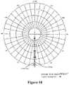
- Fig. 10is a diagram of angle distribution of light generated by the LED illuminating device of the present invention. It can be seen from Fig. 10 that the light spot generated by the LED illuminating device of the present invention has a good directivity, and a horizontal beam angle and a vertical beam angle thereof are both in a reasonable range, satisfying related provisions in the industry.
Landscapes
- Engineering & Computer Science (AREA)
- General Engineering & Computer Science (AREA)
- Mechanical Engineering (AREA)
- Physics & Mathematics (AREA)
- Microelectronics & Electronic Packaging (AREA)
- Optics & Photonics (AREA)
- Fastening Of Light Sources Or Lamp Holders (AREA)
- Led Device Packages (AREA)
- Non-Portable Lighting Devices Or Systems Thereof (AREA)
Description
- The present invention relates to an LED illuminating device, particularly used in traffic, especially used in railway traffic as a railway signal light.
- A railway signal light is used in a field environment. A train driver must be able to clearly see light emitted from the signal light at a reasonable distance in various weather conditions. Thus, the signal light must be designed to meet related national requirements. Corresponding standards of the railway signal light are established in China, wherein a horizontal beam angle of light generated by the signal light should be between -2.2° and 6°, a vertical beam angle should be between -1.02° and 6°, and a light spot generated thereby should be uniform.
- The current railway signal lights mostly use a halogen lamp as a light source, while it has a high power, and will waste a lot of energies in a long time use. In addition, there is only one halogen lamp as the light source, then, if the halogen lamp is damaged and is not timely changed, the signal light will stop working, so the operation reliability is relatively poor. A signal light taking an LED as a light source is also available in the current market, and the light source of such signal light usually consists of a plurality of LEDs. As there is inevitably a certain spatial distance between the LEDs, light emitted from respective LED of the light source will generate a light point which cannot be well eliminated with a lens of a traditional signal light for obtaining a uniform light spot. However, such light points make it quite difficult for secondary optical design of the signal light. The earlier patent application
US2011/0141725A1 discloses an illumination system which has a concentrator with a double-cone shape. However, with such a concentrator, the system is not compact. The earlier patent applicationEP 1988329 A1 discloses an illumination device. Light emitting device modules illuminate at wide angle in the longitudinal direction of a lighting fixture. The lighting fixture is provided with a light emitting device module having a light emitting device, an installation member for mounting multiple light emitting device modules thereon, and a support for supporting the installation member. The installation member is bent in multiple stages, so that the light beams from the multiple light emitting device modules mounted on the installation member are pointed to multiple different directions. - In order to solve the above problems, the present invention provides an LED illuminating device which is used particularly in traffic, especially in railway traffic as a railway signal light. The LED illuminating device of the present invention, when used as a signal light, is able to generate a uniform light spot and well satisfy related industry provisions.
- The object of the present invention is accomplished via an LED illuminating device. The LED illuminating device comprises a printed circuit board, and at least one LED chip group arranged on the printed circuit board and a lens assembly. In addition, the LED illuminating device further comprises a reflector provided between the LED chip group and the lens assembly for diffusely reflecting light from the LED chip group so that the light is uniformized and emerges in a direction of the lens assembly. In one solution of the present invention, light from respective LED chips of the LED chip group firstly is diffusely reflected by the reflector so as to eliminate light points formed by light from respective LED chips and to make output light more uniform, thereby the LED chip group is enabled to generate a uniform light spot.
- Preferably, the reflector is a plate-shaped body with a via, wherein the via is formed with an accommodation opening for the LED chip group at one side thereof facing the printed circuit board, and formed with a light emergent opening at the other side opposite to the one side, wherein an inner wall of the via forms a diffuse reflective region that can effectively diffusely reflect light from respective LED chips so as to eliminate the light points. The via has a dimension gradually reduced from the accommodation opening to the light emergent opening. Since the LED chip group is directly placed in the accommodation opening, light from the LED chip group will not directly emerge from the light emergent opening as it is blocked by the diffuse reflective region, which therefore effectively prevents formation of the light points.
- Optionally, the light emergent opening is circular for forming a circular light spot.
- According to a preferred solution of the present invention, the LED chip group comprises a primary LED chip group and a redundant LED chip group, wherein the primary LED chip group and the redundant LED chip group consist of two LED chips, respectively, the four LED chips are arranged in a square on the printed circuit board, and the LED chips in the same group are arranged at same diagonal of the square. In order to try to make the light points formed by light from respective LED chips to be not easily identified, the LED chips are arranged as closely to each other as is possible. Two LED chip groups are used in one solution of the present invention because a redundant LED chip group can greatly improve the safety coefficient of the whole LED illuminating device since the LED illuminating device as a signal light is usually used in a field environment, the operation condition is bad, and the railway traffic might be adversely affected if the LED chip as a light source is failed.
- Preferably, the accommodation opening is a square opening that has a dimension bigger than or equal to a dimension of the LED chip group. As the LED chips are just against the square opening, it further prevents light from the LED chips from directly emerging from the light emergent opening.
- According to the present invention, a projection is provided at the other side of the reflector away from the printed circuit board, and the light emergent opening is opened on the projection. A distance between the light emergent opening and the accommodation opening is increased by forming the projection, thus an area of the diffuse reflective region is prominently increased, and light from the LED chips can be diffusely reflected more sufficiently.
- According to a preferred solution of the present invention, the LED illuminating device further comprises an attachment lens provided between the reflector and the lens assembly. The attachment lens further uniformizes light diffusely reflected by the reflector so as to eliminate the light points.
- Preferably, the attachment lens has a microlens array including a plurality of microlenses which are in a honeycomb arrangement, wherein respective microlens in the microlens array is a spherical lens.
- Advantageously, the lens assembly consists of a first Fresnel lens and a second Fresnel lens arranged in sequential in a light emerging direction. The lens assembly formed jointly by the two Fresnel lenses results in an effect of a convex, serving a function of focusing light diffusely reflected by the reflector so as to render a stronger directivity of light from the LED illuminating device.
- Preferably, the reflector is made from a PC material, and of course, the reflector also can be made from other materials that can perform a diffuse reflection.
- The accompanying drawings constitute a part of the present Description and are used to provide further understanding of the present invention. Such accompanying drawings illustrate the embodiments of the present invention and are used to describe the principles of the present invention together with the Description. In the accompanying drawings the same components are represented by the same reference numbers. As shown in the drawings:
Fig. 1 is an exploded schematic diagram of an LED illuminating device of the present invention;Fig. 2 is a schematic diagram of one side of a reflector of an LED illuminating device of the present invention;Fig. 3 is a schematic diagram of the other side of the reflector of the LED illuminating device of the present invention;Fig. 4 is a schematic diagram of an LED chip group of an LED illuminating device of the present invention;Fig. 5 is a schematic diagram of an attachment lens of an LED illuminating device of the present invention;Fig. 6 is a local enlarged view of an attachment lens;Fig. 7 is a sectional view of an attachment lens;Fig. 8 is a local enlarged view of the sectional view shown inFig. 7 ;Fig. 9 is a diagram of light intensity distribution of light generated by an LED illuminating device of the present invention; andFig. 10 is a diagram of angle distribution of light generated by an LED illuminating device of the present invention.Fig. 1 is an exploded schematic diagram of an LED illuminating device of the present invention. It can be seen fromFig. 1 that the LED illuminating device of the present invention comprises a printed circuit board 1, and at least oneLED chip group 2 arranged on the printed circuit board 1 and alens assembly 4. Besides, the LED illuminating device further comprisesreflector 3 provided between theLED chip group 2 and thelens assembly 4 for diffusely reflecting light from theLED chip group 2 so that the light is uniformized and emerges in a direction of thelens assembly 4. In one solution of the present invention, thelens assembly 4 consists of a first Fresnellens 4a and a second Fresnellens 4b arranged in sequential in a light emerging direction. Thelens assembly 4 formed jointly by the two Fresnellenses reflector 3 so as to render a stronger directivity of light from the LED illuminating device. Besides, anattachment lens 5 is further provided between thereflector 3 and thelens assembly 4.Fig. 2 and Fig. 3 are schematic diagrams of two sides of thereflector 3 of the LED illuminating device of the present invention, respectively. As can be seen fromFig. 2 and Fig. 3 , thereflector 3 is a plate-shaped body with a via 3a, wherein the via 3a is formed with anaccommodation opening 3b for theLED chip group 2 at one side thereof facing the printed circuit board 1 (seeFig. 2 ) and formed with a lightemergent opening 3c at the other side opposite to the one side (seeFig. 3 ), wherein an inner wall of the via 3a forms a diffusereflective region 3d. In addition, it can be seen fromFig. 2 that the via 3a has a dimension gradually reduced from theaccommodation opening 3b to the lightemergent opening 3c. In one solution of the present invention, thereflector 3 is made from a PC material, and of course, it also can be made from other types of diffusing materials.- It can be seen from
Fig. 3 that a projection is provided at the other side of thereflector 3 away from the printed circuit board 1, and the lightemergent opening 3c is opened on the projection. An incident surface of theattachment lens 5 is directly against the projection when the LED illuminating device of the present invention is assembled. - In addition, it can be seen from
Fig. 2 and Fig. 3 that the lightemergent opening 3c is circular, which is quite favorable for forming a circular light spot. Besides, theaccommodation opening 3b is a square opening. Fig. 4 is a schematic diagram of theLED chip group 2 of the LED illuminating device of the present invention. According to the present invention, theLED chip group 2 comprises a primaryLED chip group 2a and a redundantLED chip group 2b, wherein the primaryLED chip group 2a consists of twoLED chips 2a', 2a" and the redundantLED chip group 2b consists of twoLED chips 2b', 2b'', theLED chips 2a', 2a" and 2b', 2b" are arranged in a square on the printed circuit board 1, and theLED chips 2a' , 2a" and 2b' , 2b" in the same group are arranged at two ends of the same diagonal of the square. TheLED chips 2a', 2a" and 2b', 2b" are arranged to be directly as closely to each other as is possible. OSLON LED chips of OSRAM are used in one solution of the present invention, by which a distance between edges of adjacent chips is 0.89mm. Of course, other types of LED chips also can be used. The adjacent chips should be arranged to be close if the processing condition allows.- In addition, in order to try to prevent light from directly emerging from the light
emergent opening 3c, thesquare accommodation opening 3b is a square opening that has a dimension bigger than or equal to that of theLED chip group 2. - Further,
Fig. 5 - Fig. 8 specifically show schematic diagrams of theattachment lens 5. As can be seen fromFig. 5 , theattachment lens 5 has a microlens array including a plurality ofmicrolenses 5a which are in a honeycomb arrangement, whereinFig. 6 is a local enlarged view of the microlens array, from which it can be seen thatrespective microlens 5a has an outline of a regular hexagon, wherein a distance between two opposite sides is 0.6mm, and of course, a dimension of the regular hexagon also can be correspondingly adjusted according to requirements.Fig. 7 is a sectional view of theattachment lens 5, andFig. 8 is a local enlarged view of the sectional view shown inFig. 7 . It can be seen fromFig. 8 thatrespective microlens 5a in the microlens array is a spherical lens. Fig. 9 is a diagram of light intensity distribution of light generated by the LED illuminating device of the present invention. As can be seen fromFig. 9 , a light spot generated by the LED illuminating device of the present invention is quite uniform within an angle range between -4.5° and 4.5°.Fig. 10 is a diagram of angle distribution of light generated by the LED illuminating device of the present invention. It can be seen fromFig. 10 that the light spot generated by the LED illuminating device of the present invention has a good directivity, and a horizontal beam angle and a vertical beam angle thereof are both in a reasonable range, satisfying related provisions in the industry.- The above is merely preferred embodiments of the present invention but not to limit the present invention. For the person skilled in the art, the present invention may have various alterations and changes. Any alterations, equivalent substitutions, improvements, within the spirit and principle of the present invention, should be covered in the protection scope of the present invention.
- 1
- printed circuit board
- 2
- LED chip group
- 2a
- primary LED chip group
- 2b
- redundant LED chip group
- 2a', 2a"; 2b, 2b"
- LED chip
- 3
- reflector
- 3a
- via
- 3b
- accommodation opening
- 3c
- light emergent opening
- 3d
- diffuse reflective region
- 4
- lens assembly
- 4a
- first Fresnel lens
- 4b
- second Fresnel lens
- 5
- attachment lens
- 5a
- microlens
Claims (9)
- An LED illuminating device, comprising a printed circuit board (1), and at least one LED chip group (2) arranged on the printed circuit board (1) and a lens assembly (4), wherein the LED illuminating device further comprises a reflector (3) provided between the LED chip group (2) and the lens assembly (4), wherein the reflector (3) is configured to diffusely reflect light from the LED chip group (2) so that the light is uniformized and emerges in a direction of the lens assembly (4), wherein the reflector (3) is a plate-shaped body with a via (3a), wherein the via (3a) is formed with an accommodation opening (3b) for the LED chip group (2) at one side thereof facing the printed circuit board (1), and formed with a light emergent opening (3c) at the other side opposite to the one side, wherein an inner wall of the via (3a) forms a diffuse reflective region (3d),characterized in that the via (3a) has a dimension gradually reduced from the accommodation opening (3b) to the light emergent opening (3c).
- The LED illuminating device according to Claim 1,characterized in that the light emergent opening (3c) is circular.
- The LED illuminating device according to Claim 1,characterized in that the LED chip group (2) comprises a primary LED chip group (2a) and a redundant LED chip group (2b), wherein the primary LED chip group (2a) and the redundant LED chip group (2b) consist of two LED chips (2a', 2a" ; 2b', 2b"), respectively, the LED chips (2a', 2a"; 2b', 2b") are arranged in a square on the printed circuit board (1), and the LED chips (2a', 2a"; 2b', 2b") in the same group are arranged at diagonal of the square.
- The LED illuminating device according to Claim 3,characterized in that the accommodation opening (3b) is a square opening that has a dimension bigger than or equal to a dimension of the LED chip group (2).
- The LED illuminating device according to Claim 1,characterized in that a projection is provided at the other side of the reflector (3) away from the printed circuit board (1), and the light emergent opening (3c) is opened on the projection.
- The LED illuminating device according to any one of Claims 1-5,characterized in that the LED illuminating device further comprises an attachment lens (5) provided between the reflector (3) and the lens assembly (4).
- The LED illuminating device according to Claim 6,characterized in that the attachment lens (5) has a microlens array including a plurality of microlenses (5a) which are in a honeycomb arrangement, wherein respective microlens (5a) is a spherical lens.
- The LED illuminating device according to any one of Claims 1-5,characterized in that the lens assembly (4) consists of a first Fresnel lens (4a) and a second Fresnel lens (4b) arranged in sequential in a light emerging direction.
- The LED illuminating device according to any one of Claims 1-5,characterized in that the reflector (3) is made from a PC material.
Applications Claiming Priority (2)
| Application Number | Priority Date | Filing Date | Title |
|---|---|---|---|
| CN201110366671.6ACN103123067B (en) | 2011-11-17 | LED light device | |
| PCT/EP2012/072770WO2013072429A1 (en) | 2011-11-17 | 2012-11-15 | Led illuminating device |
Publications (2)
| Publication Number | Publication Date |
|---|---|
| EP2780627A1 EP2780627A1 (en) | 2014-09-24 |
| EP2780627B1true EP2780627B1 (en) | 2017-11-08 |
Family
ID=47351577
Family Applications (1)
| Application Number | Title | Priority Date | Filing Date |
|---|---|---|---|
| EP12799092.7ANot-in-forceEP2780627B1 (en) | 2011-11-17 | 2012-11-15 | Led illuminating device |
Country Status (3)
| Country | Link |
|---|---|
| US (1) | US9360192B2 (en) |
| EP (1) | EP2780627B1 (en) |
| WO (1) | WO2013072429A1 (en) |
Families Citing this family (6)
| Publication number | Priority date | Publication date | Assignee | Title |
|---|---|---|---|---|
| US8974077B2 (en) | 2012-07-30 | 2015-03-10 | Ultravision Technologies, Llc | Heat sink for LED light source |
| US9195281B2 (en) | 2013-12-31 | 2015-11-24 | Ultravision Technologies, Llc | System and method for a modular multi-panel display |
| CN104566048A (en)* | 2015-01-30 | 2015-04-29 | 李达 | Illuminating system based on cloud light effect |
| DE102015001695A1 (en)* | 2015-02-10 | 2016-08-11 | Audi Ag | Lighting device for a headlight of a motor vehicle and method for operating a lighting device |
| KR101737321B1 (en)* | 2015-03-23 | 2017-05-22 | (주)엔디에스 | Condensing lighting device |
| EP3480078B1 (en)* | 2017-11-07 | 2021-06-30 | Siemens Mobility AG | Light signal and method for displaying signal terms for a traffic route |
Citations (4)
| Publication number | Priority date | Publication date | Assignee | Title |
|---|---|---|---|---|
| EP1988329A1 (en)* | 2006-02-20 | 2008-11-05 | Stanley Electric Co., Ltd. | Illumination device |
| AT505154A4 (en)* | 2007-10-09 | 2008-11-15 | Swarco Futurit Verkehrssignals | OPTICAL SIGNALING DEVICE |
| WO2009055374A1 (en)* | 2007-10-25 | 2009-04-30 | Lsi Industries, Inc. | Reflector |
| WO2009063382A1 (en)* | 2007-11-13 | 2009-05-22 | Koninklijke Philips Electronics N.V. | A lighting panel |
Family Cites Families (7)
| Publication number | Priority date | Publication date | Assignee | Title |
|---|---|---|---|---|
| JP4829230B2 (en) | 2004-08-06 | 2011-12-07 | コーニンクレッカ フィリップス エレクトロニクス エヌ ヴィ | Light engine |
| US7553044B2 (en) | 2006-05-25 | 2009-06-30 | Ansaldo Sts Usa, Inc. | Light emitting diode signaling device and method of providing an indication using the same |
| US8240875B2 (en)* | 2008-06-25 | 2012-08-14 | Cree, Inc. | Solid state linear array modules for general illumination |
| CN201680227U (en) | 2009-12-10 | 2010-12-22 | 联嘉光电股份有限公司 | Mixed light type traffic light |
| US8439526B2 (en) | 2009-12-11 | 2013-05-14 | Zinovi Brusilovsky | Variable-color lighting system |
| CN102315371A (en)* | 2010-07-05 | 2012-01-11 | 松下电工株式会社 | Light-emitting device |
| JP5849193B2 (en)* | 2011-05-31 | 2016-01-27 | パナソニックIpマネジメント株式会社 | Light emitting device, surface light source, liquid crystal display device, and lens |
- 2012
- 2012-11-15EPEP12799092.7Apatent/EP2780627B1/ennot_activeNot-in-force
- 2012-11-15WOPCT/EP2012/072770patent/WO2013072429A1/enactiveApplication Filing
- 2012-11-15USUS14/358,226patent/US9360192B2/ennot_activeExpired - Fee Related
Patent Citations (4)
| Publication number | Priority date | Publication date | Assignee | Title |
|---|---|---|---|---|
| EP1988329A1 (en)* | 2006-02-20 | 2008-11-05 | Stanley Electric Co., Ltd. | Illumination device |
| AT505154A4 (en)* | 2007-10-09 | 2008-11-15 | Swarco Futurit Verkehrssignals | OPTICAL SIGNALING DEVICE |
| WO2009055374A1 (en)* | 2007-10-25 | 2009-04-30 | Lsi Industries, Inc. | Reflector |
| WO2009063382A1 (en)* | 2007-11-13 | 2009-05-22 | Koninklijke Philips Electronics N.V. | A lighting panel |
Also Published As
| Publication number | Publication date |
|---|---|
| US9360192B2 (en) | 2016-06-07 |
| CN103123067A (en) | 2013-05-29 |
| WO2013072429A1 (en) | 2013-05-23 |
| US20140313740A1 (en) | 2014-10-23 |
| EP2780627A1 (en) | 2014-09-24 |
Similar Documents
| Publication | Publication Date | Title |
|---|---|---|
| EP2780627B1 (en) | Led illuminating device | |
| EP2771729B1 (en) | A lens and an asymmetrical light distribution illuminating device having such lens | |
| JP5212947B2 (en) | Ambient lighting system | |
| US9518705B2 (en) | Lens and an illumination device having the lens | |
| US20030193807A1 (en) | LED-based elevated omnidirectional airfield light | |
| CA2538529A1 (en) | Parking garage luminaire with interchangeable reflector modules | |
| US20130120991A1 (en) | Lighting module for illuminating traffic routes, and traffic route luminaire | |
| US8591079B2 (en) | LED ceiling lamp | |
| TWI534391B (en) | Light-guiding structure and light-emitting device | |
| US10295151B2 (en) | Optical member for spot flood lights | |
| CN104124239A (en) | Light emitting diode module | |
| CN106524079A (en) | Lens and LED lamp using same | |
| WO2014086782A1 (en) | Lens, omnidirectional illuminating device having the lens and retrofit lamp | |
| EP2034237B1 (en) | Energy-saving lampshade with even light distribution | |
| WO2018000285A1 (en) | Lighting fixture | |
| KR101723164B1 (en) | Led luminaire | |
| HUP0900709A2 (en) | Led-luminaire | |
| GB2468118A (en) | Light emitting diode lighting device employing multiple reflectors | |
| CN104676472B (en) | Lens assembly and lamp applying same | |
| CN102954362A (en) | LED bulb with all-dimensional illumination function | |
| CN103791252B (en) | Light-emitting module and illuminating apparatus and lamp box including light-emitting module | |
| CN102345811B (en) | lighting equipment | |
| CN203099686U (en) | Lens, LED (light-emitting diode) module and illuminating system using LED module | |
| CN105782902A (en) | Lens, lens module and lamp | |
| KR20160104473A (en) | Intelligent LED headlight for railway vehicles |
Legal Events
| Date | Code | Title | Description |
|---|---|---|---|
| PUAI | Public reference made under article 153(3) epc to a published international application that has entered the european phase | Free format text:ORIGINAL CODE: 0009012 | |
| 17P | Request for examination filed | Effective date:20140617 | |
| AK | Designated contracting states | Kind code of ref document:A1 Designated state(s):AL AT BE BG CH CY CZ DE DK EE ES FI FR GB GR HR HU IE IS IT LI LT LU LV MC MK MT NL NO PL PT RO RS SE SI SK SM TR | |
| DAX | Request for extension of the european patent (deleted) | ||
| 17Q | First examination report despatched | Effective date:20170109 | |
| REG | Reference to a national code | Ref country code:DE Ref legal event code:R079 Ref document number:602012039566 Country of ref document:DE Free format text:PREVIOUS MAIN CLASS: F21K0099000000 Ipc:B61L0005180000 | |
| RIC1 | Information provided on ipc code assigned before grant | Ipc:F21Y 115/10 20160101ALI20170511BHEP Ipc:F21V 13/04 20060101ALI20170511BHEP Ipc:B61L 5/18 20060101AFI20170511BHEP Ipc:F21K 9/60 20160101ALI20170511BHEP Ipc:F21K 9/62 20160101ALI20170511BHEP | |
| GRAP | Despatch of communication of intention to grant a patent | Free format text:ORIGINAL CODE: EPIDOSNIGR1 | |
| INTG | Intention to grant announced | Effective date:20170703 | |
| GRAS | Grant fee paid | Free format text:ORIGINAL CODE: EPIDOSNIGR3 | |
| GRAA | (expected) grant | Free format text:ORIGINAL CODE: 0009210 | |
| AK | Designated contracting states | Kind code of ref document:B1 Designated state(s):AL AT BE BG CH CY CZ DE DK EE ES FI FR GB GR HR HU IE IS IT LI LT LU LV MC MK MT NL NO PL PT RO RS SE SI SK SM TR | |
| REG | Reference to a national code | Ref country code:GB Ref legal event code:FG4D | |
| REG | Reference to a national code | Ref country code:CH Ref legal event code:EP Ref country code:AT Ref legal event code:REF Ref document number:943851 Country of ref document:AT Kind code of ref document:T Effective date:20171115 | |
| REG | Reference to a national code | Ref country code:IE Ref legal event code:FG4D | |
| REG | Reference to a national code | Ref country code:DE Ref legal event code:R096 Ref document number:602012039566 Country of ref document:DE | |
| REG | Reference to a national code | Ref country code:NL Ref legal event code:MP Effective date:20171108 | |
| REG | Reference to a national code | Ref country code:LT Ref legal event code:MG4D | |
| REG | Reference to a national code | Ref country code:AT Ref legal event code:MK05 Ref document number:943851 Country of ref document:AT Kind code of ref document:T Effective date:20171108 | |
| PG25 | Lapsed in a contracting state [announced via postgrant information from national office to epo] | Ref country code:ES Free format text:LAPSE BECAUSE OF FAILURE TO SUBMIT A TRANSLATION OF THE DESCRIPTION OR TO PAY THE FEE WITHIN THE PRESCRIBED TIME-LIMIT Effective date:20171108 Ref country code:LT Free format text:LAPSE BECAUSE OF FAILURE TO SUBMIT A TRANSLATION OF THE DESCRIPTION OR TO PAY THE FEE WITHIN THE PRESCRIBED TIME-LIMIT Effective date:20171108 Ref country code:NL Free format text:LAPSE BECAUSE OF FAILURE TO SUBMIT A TRANSLATION OF THE DESCRIPTION OR TO PAY THE FEE WITHIN THE PRESCRIBED TIME-LIMIT Effective date:20171108 Ref country code:NO Free format text:LAPSE BECAUSE OF FAILURE TO SUBMIT A TRANSLATION OF THE DESCRIPTION OR TO PAY THE FEE WITHIN THE PRESCRIBED TIME-LIMIT Effective date:20180208 Ref country code:SE Free format text:LAPSE BECAUSE OF FAILURE TO SUBMIT A TRANSLATION OF THE DESCRIPTION OR TO PAY THE FEE WITHIN THE PRESCRIBED TIME-LIMIT Effective date:20171108 Ref country code:FI Free format text:LAPSE BECAUSE OF FAILURE TO SUBMIT A TRANSLATION OF THE DESCRIPTION OR TO PAY THE FEE WITHIN THE PRESCRIBED TIME-LIMIT Effective date:20171108 | |
| PG25 | Lapsed in a contracting state [announced via postgrant information from national office to epo] | Ref country code:GR Free format text:LAPSE BECAUSE OF FAILURE TO SUBMIT A TRANSLATION OF THE DESCRIPTION OR TO PAY THE FEE WITHIN THE PRESCRIBED TIME-LIMIT Effective date:20180209 Ref country code:RS Free format text:LAPSE BECAUSE OF FAILURE TO SUBMIT A TRANSLATION OF THE DESCRIPTION OR TO PAY THE FEE WITHIN THE PRESCRIBED TIME-LIMIT Effective date:20171108 Ref country code:LV Free format text:LAPSE BECAUSE OF FAILURE TO SUBMIT A TRANSLATION OF THE DESCRIPTION OR TO PAY THE FEE WITHIN THE PRESCRIBED TIME-LIMIT Effective date:20171108 Ref country code:AT Free format text:LAPSE BECAUSE OF FAILURE TO SUBMIT A TRANSLATION OF THE DESCRIPTION OR TO PAY THE FEE WITHIN THE PRESCRIBED TIME-LIMIT Effective date:20171108 Ref country code:IS Free format text:LAPSE BECAUSE OF FAILURE TO SUBMIT A TRANSLATION OF THE DESCRIPTION OR TO PAY THE FEE WITHIN THE PRESCRIBED TIME-LIMIT Effective date:20180308 Ref country code:HR Free format text:LAPSE BECAUSE OF FAILURE TO SUBMIT A TRANSLATION OF THE DESCRIPTION OR TO PAY THE FEE WITHIN THE PRESCRIBED TIME-LIMIT Effective date:20171108 Ref country code:BG Free format text:LAPSE BECAUSE OF FAILURE TO SUBMIT A TRANSLATION OF THE DESCRIPTION OR TO PAY THE FEE WITHIN THE PRESCRIBED TIME-LIMIT Effective date:20180208 | |
| PG25 | Lapsed in a contracting state [announced via postgrant information from national office to epo] | Ref country code:DK Free format text:LAPSE BECAUSE OF FAILURE TO SUBMIT A TRANSLATION OF THE DESCRIPTION OR TO PAY THE FEE WITHIN THE PRESCRIBED TIME-LIMIT Effective date:20171108 Ref country code:EE Free format text:LAPSE BECAUSE OF FAILURE TO SUBMIT A TRANSLATION OF THE DESCRIPTION OR TO PAY THE FEE WITHIN THE PRESCRIBED TIME-LIMIT Effective date:20171108 Ref country code:SK Free format text:LAPSE BECAUSE OF FAILURE TO SUBMIT A TRANSLATION OF THE DESCRIPTION OR TO PAY THE FEE WITHIN THE PRESCRIBED TIME-LIMIT Effective date:20171108 Ref country code:CY Free format text:LAPSE BECAUSE OF FAILURE TO SUBMIT A TRANSLATION OF THE DESCRIPTION OR TO PAY THE FEE WITHIN THE PRESCRIBED TIME-LIMIT Effective date:20171108 Ref country code:CH Free format text:LAPSE BECAUSE OF NON-PAYMENT OF DUE FEES Effective date:20171130 Ref country code:CZ Free format text:LAPSE BECAUSE OF FAILURE TO SUBMIT A TRANSLATION OF THE DESCRIPTION OR TO PAY THE FEE WITHIN THE PRESCRIBED TIME-LIMIT Effective date:20171108 Ref country code:LI Free format text:LAPSE BECAUSE OF NON-PAYMENT OF DUE FEES Effective date:20171130 | |
| REG | Reference to a national code | Ref country code:DE Ref legal event code:R097 Ref document number:602012039566 Country of ref document:DE | |
| PG25 | Lapsed in a contracting state [announced via postgrant information from national office to epo] | Ref country code:LU Free format text:LAPSE BECAUSE OF NON-PAYMENT OF DUE FEES Effective date:20171115 Ref country code:RO Free format text:LAPSE BECAUSE OF FAILURE TO SUBMIT A TRANSLATION OF THE DESCRIPTION OR TO PAY THE FEE WITHIN THE PRESCRIBED TIME-LIMIT Effective date:20171108 Ref country code:IT Free format text:LAPSE BECAUSE OF FAILURE TO SUBMIT A TRANSLATION OF THE DESCRIPTION OR TO PAY THE FEE WITHIN THE PRESCRIBED TIME-LIMIT Effective date:20171108 Ref country code:PL Free format text:LAPSE BECAUSE OF FAILURE TO SUBMIT A TRANSLATION OF THE DESCRIPTION OR TO PAY THE FEE WITHIN THE PRESCRIBED TIME-LIMIT Effective date:20171108 Ref country code:SM Free format text:LAPSE BECAUSE OF FAILURE TO SUBMIT A TRANSLATION OF THE DESCRIPTION OR TO PAY THE FEE WITHIN THE PRESCRIBED TIME-LIMIT Effective date:20171108 | |
| REG | Reference to a national code | Ref country code:BE Ref legal event code:MM Effective date:20171130 | |
| REG | Reference to a national code | Ref country code:IE Ref legal event code:MM4A | |
| PLBE | No opposition filed within time limit | Free format text:ORIGINAL CODE: 0009261 | |
| STAA | Information on the status of an ep patent application or granted ep patent | Free format text:STATUS: NO OPPOSITION FILED WITHIN TIME LIMIT | |
| PG25 | Lapsed in a contracting state [announced via postgrant information from national office to epo] | Ref country code:MT Free format text:LAPSE BECAUSE OF NON-PAYMENT OF DUE FEES Effective date:20171115 | |
| REG | Reference to a national code | Ref country code:FR Ref legal event code:ST Effective date:20180905 | |
| 26N | No opposition filed | Effective date:20180809 | |
| GBPC | Gb: european patent ceased through non-payment of renewal fee | Effective date:20180208 | |
| PG25 | Lapsed in a contracting state [announced via postgrant information from national office to epo] | Ref country code:FR Free format text:LAPSE BECAUSE OF NON-PAYMENT OF DUE FEES Effective date:20180108 Ref country code:IE Free format text:LAPSE BECAUSE OF NON-PAYMENT OF DUE FEES Effective date:20171115 | |
| PG25 | Lapsed in a contracting state [announced via postgrant information from national office to epo] | Ref country code:BE Free format text:LAPSE BECAUSE OF NON-PAYMENT OF DUE FEES Effective date:20171130 Ref country code:SI Free format text:LAPSE BECAUSE OF FAILURE TO SUBMIT A TRANSLATION OF THE DESCRIPTION OR TO PAY THE FEE WITHIN THE PRESCRIBED TIME-LIMIT Effective date:20171108 | |
| PGFP | Annual fee paid to national office [announced via postgrant information from national office to epo] | Ref country code:DE Payment date:20181120 Year of fee payment:7 | |
| PG25 | Lapsed in a contracting state [announced via postgrant information from national office to epo] | Ref country code:GB Free format text:LAPSE BECAUSE OF NON-PAYMENT OF DUE FEES Effective date:20180208 | |
| PG25 | Lapsed in a contracting state [announced via postgrant information from national office to epo] | Ref country code:HU Free format text:LAPSE BECAUSE OF FAILURE TO SUBMIT A TRANSLATION OF THE DESCRIPTION OR TO PAY THE FEE WITHIN THE PRESCRIBED TIME-LIMIT; INVALID AB INITIO Effective date:20121115 Ref country code:MC Free format text:LAPSE BECAUSE OF FAILURE TO SUBMIT A TRANSLATION OF THE DESCRIPTION OR TO PAY THE FEE WITHIN THE PRESCRIBED TIME-LIMIT Effective date:20171108 | |
| PG25 | Lapsed in a contracting state [announced via postgrant information from national office to epo] | Ref country code:MK Free format text:LAPSE BECAUSE OF FAILURE TO SUBMIT A TRANSLATION OF THE DESCRIPTION OR TO PAY THE FEE WITHIN THE PRESCRIBED TIME-LIMIT Effective date:20171108 | |
| PG25 | Lapsed in a contracting state [announced via postgrant information from national office to epo] | Ref country code:TR Free format text:LAPSE BECAUSE OF FAILURE TO SUBMIT A TRANSLATION OF THE DESCRIPTION OR TO PAY THE FEE WITHIN THE PRESCRIBED TIME-LIMIT Effective date:20171108 | |
| PG25 | Lapsed in a contracting state [announced via postgrant information from national office to epo] | Ref country code:PT Free format text:LAPSE BECAUSE OF FAILURE TO SUBMIT A TRANSLATION OF THE DESCRIPTION OR TO PAY THE FEE WITHIN THE PRESCRIBED TIME-LIMIT Effective date:20171108 | |
| REG | Reference to a national code | Ref country code:DE Ref legal event code:R119 Ref document number:602012039566 Country of ref document:DE | |
| PG25 | Lapsed in a contracting state [announced via postgrant information from national office to epo] | Ref country code:AL Free format text:LAPSE BECAUSE OF FAILURE TO SUBMIT A TRANSLATION OF THE DESCRIPTION OR TO PAY THE FEE WITHIN THE PRESCRIBED TIME-LIMIT Effective date:20171108 | |
| PG25 | Lapsed in a contracting state [announced via postgrant information from national office to epo] | Ref country code:DE Free format text:LAPSE BECAUSE OF NON-PAYMENT OF DUE FEES Effective date:20200603 |