EP2778518B1 - Lighting device - Google Patents
Lighting deviceDownload PDFInfo
- Publication number
- EP2778518B1 EP2778518B1EP14156877.4AEP14156877AEP2778518B1EP 2778518 B1EP2778518 B1EP 2778518B1EP 14156877 AEP14156877 AEP 14156877AEP 2778518 B1EP2778518 B1EP 2778518B1
- Authority
- EP
- European Patent Office
- Prior art keywords
- light radiation
- lighting device
- circuit board
- base wall
- housing
- Prior art date
- Legal status (The legal status is an assumption and is not a legal conclusion. Google has not performed a legal analysis and makes no representation as to the accuracy of the status listed.)
- Not-in-force
Links
- 230000005855radiationEffects0.000claimsdescription53
- 239000000463materialSubstances0.000claimsdescription18
- 239000000758substrateSubstances0.000claimsdescription17
- 230000003287optical effectEffects0.000claimsdescription14
- 229910052782aluminiumInorganic materials0.000claimsdescription9
- XAGFODPZIPBFFR-UHFFFAOYSA-NaluminiumChemical compound[Al]XAGFODPZIPBFFR-UHFFFAOYSA-N0.000claimsdescription9
- 229910052751metalInorganic materials0.000claimsdescription5
- 239000002184metalSubstances0.000claimsdescription5
- 239000004033plasticSubstances0.000claimsdescription5
- 239000000919ceramicSubstances0.000claimsdescription4
- 239000007769metal materialSubstances0.000claimsdescription4
- 230000000284resting effectEffects0.000claims1
- 238000000034methodMethods0.000description9
- 229910010293ceramic materialInorganic materials0.000description6
- 238000010292electrical insulationMethods0.000description6
- 239000007787solidSubstances0.000description4
- 230000000694effectsEffects0.000description3
- RYGMFSIKBFXOCR-UHFFFAOYSA-NCopperChemical compound[Cu]RYGMFSIKBFXOCR-UHFFFAOYSA-N0.000description2
- 239000000853adhesiveSubstances0.000description2
- 230000001070adhesive effectEffects0.000description2
- 230000002411adverseEffects0.000description2
- 230000015572biosynthetic processEffects0.000description2
- 229910052802copperInorganic materials0.000description2
- 239000010949copperSubstances0.000description2
- 230000008878couplingEffects0.000description2
- 238000010168coupling processMethods0.000description2
- 238000005859coupling reactionMethods0.000description2
- 238000005755formation reactionMethods0.000description2
- 230000009467reductionEffects0.000description2
- OKTJSMMVPCPJKN-UHFFFAOYSA-NCarbonChemical compound[C]OKTJSMMVPCPJKN-UHFFFAOYSA-N0.000description1
- 230000002860competitive effectEffects0.000description1
- 230000007797corrosionEffects0.000description1
- 238000005260corrosionMethods0.000description1
- 239000012777electrically insulating materialSubstances0.000description1
- 230000007613environmental effectEffects0.000description1
- 230000004907fluxEffects0.000description1
- 229910002804graphiteInorganic materials0.000description1
- 239000010439graphiteSubstances0.000description1
- 238000012423maintenanceMethods0.000description1
- 239000002991molded plasticSubstances0.000description1
- 230000008520organizationEffects0.000description1
- 239000012782phase change materialSubstances0.000description1
- 230000008569processEffects0.000description1
- 238000002310reflectometryMethods0.000description1
- 238000005476solderingMethods0.000description1
- 239000000126substanceSubstances0.000description1
- 230000036967uncompetitive effectEffects0.000description1
Images


Classifications
- F—MECHANICAL ENGINEERING; LIGHTING; HEATING; WEAPONS; BLASTING
- F21—LIGHTING
- F21V—FUNCTIONAL FEATURES OR DETAILS OF LIGHTING DEVICES OR SYSTEMS THEREOF; STRUCTURAL COMBINATIONS OF LIGHTING DEVICES WITH OTHER ARTICLES, NOT OTHERWISE PROVIDED FOR
- F21V17/00—Fastening of component parts of lighting devices, e.g. shades, globes, refractors, reflectors, filters, screens, grids or protective cages
- F21V17/10—Fastening of component parts of lighting devices, e.g. shades, globes, refractors, reflectors, filters, screens, grids or protective cages characterised by specific fastening means or way of fastening
- F21V17/12—Fastening of component parts of lighting devices, e.g. shades, globes, refractors, reflectors, filters, screens, grids or protective cages characterised by specific fastening means or way of fastening by screwing
- F—MECHANICAL ENGINEERING; LIGHTING; HEATING; WEAPONS; BLASTING
- F21—LIGHTING
- F21V—FUNCTIONAL FEATURES OR DETAILS OF LIGHTING DEVICES OR SYSTEMS THEREOF; STRUCTURAL COMBINATIONS OF LIGHTING DEVICES WITH OTHER ARTICLES, NOT OTHERWISE PROVIDED FOR
- F21V19/00—Fastening of light sources or lamp holders
- F21V19/001—Fastening of light sources or lamp holders the light sources being semiconductors devices, e.g. LEDs
- F21V19/003—Fastening of light source holders, e.g. of circuit boards or substrates holding light sources
- F21V19/0035—Fastening of light source holders, e.g. of circuit boards or substrates holding light sources the fastening means being capable of simultaneously attaching of an other part, e.g. a housing portion or an optical component
- F—MECHANICAL ENGINEERING; LIGHTING; HEATING; WEAPONS; BLASTING
- F21—LIGHTING
- F21V—FUNCTIONAL FEATURES OR DETAILS OF LIGHTING DEVICES OR SYSTEMS THEREOF; STRUCTURAL COMBINATIONS OF LIGHTING DEVICES WITH OTHER ARTICLES, NOT OTHERWISE PROVIDED FOR
- F21V23/00—Arrangement of electric circuit elements in or on lighting devices
- F21V23/06—Arrangement of electric circuit elements in or on lighting devices the elements being coupling devices, e.g. connectors
- F—MECHANICAL ENGINEERING; LIGHTING; HEATING; WEAPONS; BLASTING
- F21—LIGHTING
- F21V—FUNCTIONAL FEATURES OR DETAILS OF LIGHTING DEVICES OR SYSTEMS THEREOF; STRUCTURAL COMBINATIONS OF LIGHTING DEVICES WITH OTHER ARTICLES, NOT OTHERWISE PROVIDED FOR
- F21V7/00—Reflectors for light sources
- F21V7/22—Reflectors for light sources characterised by materials, surface treatments or coatings, e.g. dichroic reflectors
- F21V7/24—Reflectors for light sources characterised by materials, surface treatments or coatings, e.g. dichroic reflectors characterised by the material
- F—MECHANICAL ENGINEERING; LIGHTING; HEATING; WEAPONS; BLASTING
- F21—LIGHTING
- F21Y—INDEXING SCHEME ASSOCIATED WITH SUBCLASSES F21K, F21L, F21S and F21V, RELATING TO THE FORM OR THE KIND OF THE LIGHT SOURCES OR OF THE COLOUR OF THE LIGHT EMITTED
- F21Y2115/00—Light-generating elements of semiconductor light sources
- F21Y2115/10—Light-emitting diodes [LED]
Definitions
- the present descriptionrelates to lighting devices.
- Various embodimentsmay relate to lighting devices using LED sources as light radiation sources.
- Lighting modulessuch as those for street lighting, using solid state light radiation sources (“Solid State Lighting”, or SSL) can be considered competitive in that they simultaneously meet various requirements in terms of robustness relating to the context of their use "in the field”, namely:
- the first aspect mentioned aboveis related to the phenomena of electric overload: proper electrical insulation is important not only for avoiding the harm caused by electrostatic discharge (ESD) events during the assembly of the lighting module or of the corresponding device, but also in relation to electrical overload events such as those caused by lightning.
- ESDelectrostatic discharge
- the second aspectis related to the thermal dissipation properties of the housing which encloses the module, and may require a considerable part of the lighting device to be made of a metal material (such as aluminum) so that it has a certain degree of weight. If the module has low thermal resistance between the connection points of the light radiation sources (such as LEDs) and the thermal dissipation surface of the module, the corresponding device may also have a rather high thermal resistance between the surface in contact with the module and the external environment.
- the third aspectrelates to the faults that may arise in the module even without any causation by a specific external event. These events may have a negative effect on the service life, either in the form of "soft” faults (the light flux falls below a certain threshold level, without total loss of light emission), or in the form of "hard” faults (the radiation source ceases to emit radiation and acts as either an open or a closed contact).
- the fourth aspectrelates to the mechanical strength in the conditions of use in the field, and requires the module to meet certain requirements in terms of mechanical performance, in exterior applications for example (resistance to vibration, impact, and the like).
- electrical insulationmay be achieved by using mechanically robust substrates, with the risk of adversely affecting the thermal dissipation characteristics and increasing the possibility of hard faults; on the other hand, materials capable of providing electrical insulation together with good thermal dissipation characteristics while also reducing the risks of hard faults may be mechanically fragile.
- substrates of the PCB (printed circuit board) typein other words those resembling printed circuits, with metal cores, using high luminosity LEDs as the light radiation sources. Solutions of this kind have good characteristics in terms of thermal dissipation, electrical insulation and mechanical robustness.
- CTEcoefficient of thermal expansion
- the specified values of 100 kilohoursmay fall to values of 20 - 30 kilohours when measured in the field.
- a performance substantially comparable to that of copper, in terms of the mismatch of the coefficient of thermal expansion (CTE) with respect to packages of ceramic material,can be achieved by using the material known as FR4, although the latter has a low level of thermal dissipation; attempts may be made to counteract this characteristic by providing thermal bridges ("vias") through the PCB, but this has negative effects on the electrical insulation characteristics.
- CTEcoefficient of thermal expansion
- PCB substrates of ceramic materialshould be used, as these can provide high performance in terms of thermal characteristics, electrical insulation and the service life of the module, but this would have adverse effects on the mechanical characteristics, particularly where the possibility of using large PCBs is being considered.
- Chip On Board(CoB) products appears more promising, although these products are uncompetitive, at the present time at least, in terms of the lighting density (known as the cost per lumen), while they do not allow a high chip density in the CoB.
- Various embodimentsmay be based on the provision of at least one element (made in the form of a reflector, for example) which can act simultaneously to provide not only optical functions, but also mechanical and electrical functions, allowing in all cases the use of solid state light radiation sources, such as high luminosity LEDs, as light radiation sources.
- These sourcesmay be, for example, LEDs which are not mounted in a package but are simply placed on a substrate, for example one resembling a printed circuit board (PCB), fitted in a housing of plastic or metal material.
- PCBprinted circuit board
- Various embodimentsmay be applied to solutions in which the light radiation sources are installed in an area which is sufficiently small to provide adequate properties of mechanical robustness for the support, of the PCB type for example.
- the aforesaid elementmay have:
- a lighting device 10which can be used, for example, for street lighting applications.
- the device 10can be mounted on a support P such as a pole, a bracket, an overhead line, or the like, according to the procedures currently used in the lighting field.
- the device 10may be intended for fitting into a containment structure S which in turn is intended to be fastened to the support P and serves to protect the device 10, while also allowing the light radiation emitted by the latter to be projected into the environment.
- This containment structure Sshown schematically in broken lines in Figure 7 only, mounted on a support P, may be of any known type. It is therefore unnecessary to give a detailed description in this document, especially since the characteristics of this containment structure are not particularly relevant to the embodiments.
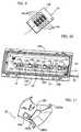
- a lighting device 10 as illustratedmay include a tray-like containment housing 12 (of rectangular shape, for example), having a base wall 12a.
- one or more light radiation sources 14, of the LED type for example,may be applied to the base wall 12a of the housing 12.
- the light radiation sources 14may be electrically powered through electrical contact pads 14a provided, for example, on a plate-like substrate 140 so as to be placed in an opposite position from the base wall 12a of the housing 12.
- a circuit board 16which can be made, for example, by procedures substantially similar to those used for a printed circuit board (PCB), may have electrically conductive tracks (or lines) 160.
- the conductive lines 160may extend on the opposite face of the board 16 from the base wall 12a of the housing 12 between respective electrical connection pads 16a.
- the electrical connection pads 16aare placed in a position facing the electrical connection pads 14a of the light radiation source or sources 14.
- one or more optical elements 18 operating by reflection and/or refractionmay be mounted in the housing 12, each element having at least one input 18a and at least one output 18b for the light radiation.
- the input 18acan be placed at the light radiation source or at one of the light radiation sources 14 so as to capture the radiation emitted by this source and then guide it toward the output or outputs 18b, thus projecting it toward the outside of the lighting device 10.
- the optical element or elements 18may take the form of one or more reflectors which can be mounted in the housing 12 with the base part 18 of the reflector, or of each reflector, (the part indicated by 18', shown more clearly in the views from below in Figures 5 and 11 ) facing the base wall 12a of the housing 12.
- the base part 18'may be provided with a base wall 180 having an aperture 180a, enabling the reflector to be fitted on a stud 120 projecting from the base wall 12a of the housing 12.
- the base wall 180(which can be made of an electrically insulating material such as plastic material, as can the whole body of the reflector 18 if required) may rest on the light radiation source or sources 14 and on the circuit board 16 (which extends adjacent to the light source or sources 14), and may press these elements against the base wall 12a.
- the reflector or reflectors 18may be locked in this assembled position by screws 120a or similar fastening formations which engage, for example, in respective holes provided in the studs 120.
- the housing 12(or at least the base wall 12a thereof) may be made of a metal material, for example aluminum, that is to say a material having good thermal dissipation characteristics.
- the circuit board 16can be made by the methods currently used to make printed circuit boards (PCBs).
- the board 16may be provided with conductive lines or tracks 160 organized so as to form anode and cathode power supply paths, respectively, for the light radiation sources (of the LED type, for example, which is the reason for the reference to the presence of an anode and a cathode), running from two power supply input pads indicated by 16b.
- the power supply input pads 16bcan receive electrical power from a power supply cable 20 which is shown in Figures 1 , 6 and 7 only, for reasons of simplicity.
- a plate-like substrate 140can be used for the sources 14, this substrate being made of ceramic material for example, and having, for example, dimensions of 20 ⁇ 30 mm, carrying, for example, eight LEDs L forming a rectangular array or "cluster" with dimensions of about 10 ⁇ 20 mm, connected in series with each other.
- Figure 9shows an exemplary embodiment in which a substrate 140 having the same dimensions of 20 ⁇ 30 mm can carry a rectangular cluster with dimensions of 10 ⁇ 20 mm formed by eight LEDs organized in four "strings", each including two LEDs L.
- two pads 14afor the anode and cathode connection respectively, may be present.
- each stringmay have respective connection pads 14a, again used for the anode and cathode connection respectively.
- a ceramic materialmay be used for the substrate 140 of the light radiation sources 14.
- a plate-like substrate of this typefor example one having dimensions such as those described above, is small enough to provide the typical advantages of ceramic materials, at lower cost, while also being capable of resisting mechanical stresses such as vibration.
- the substrate 140can be made by a method similar to that used for printed circuit boards (PCBs), for example those with metal cores.
- PCBsprinted circuit boards
- circuit board 16A similar method may be chosen for the circuit board 16; in this case, it is possible to use a PCB structure, using materials such as those known as CEM or FR4, or a flexible module structure of the type commonly known as "flex", which can be applied adhesively to the base wall 12a of the housing 12 or applied in other ways.
- a PCB structureusing materials such as those known as CEM or FR4, or a flexible module structure of the type commonly known as "flex”, which can be applied adhesively to the base wall 12a of the housing 12 or applied in other ways.
- the circuit board 16takes the form of an elongate element (in practice, a strip) extending along the array of light radiation sources 14 so as to place the pads 16a in positions facing the pads 14a.
- the board 16may be provided with cut-out parts (U-shaped, for example) 1600, in which the light radiation sources 14 are located when these light sources 14 and the circuit board 16 have been applied to the base wall 12a of the housing 12, as will be clearer from the view of Figure 10 .
- embodimentssuch as those shown in the figures (see for example Figure 7 ) may provide for the reflector, or each of the reflectors, to have a generally V-shaped configuration (or an inverted saddle shape) such that the input aperture for the radiation 18a is located next to a corresponding light radiation source 14 (in practice, at the base of the V-shape) and the output apertures 18b are located at the opposite ends of the two branches of the V-shape in a condition of substantial coplanarity with the plane of the opening of the housing 12.
- the optical element, or each of the optical elements shown here by way of example as the reflector 18can provide a plurality of functions.
- the element or each of the elements 18can provide a mechanical assembly function by pressing the light radiation source or sources 14 together with the circuit board 16 against the base wall 12a of the housing 12 so as to provide efficient heat exchange.
- the base wall 180 of the element or each of the elements 18may carry electrical contacts 1800, in the form of metal pads for example, each of which, when the respective element 18 is mounted in the housing 12 of the device (see Figure 7 ), forms a connecting bridge between two connection pads 14a, 16a of the light radiation source or of one of the light radiation sources 14 and of the circuit board 16 respectively.
- the contacts 1800may be connected to further electrical contacts 1800a capable of providing a function of electrical connection, if required, to an external power supply cable (20 in Figures 1 , 6 and 7 ) or providing possibilities of connection between different reflectors.
- the element or each of the elements 18may also provide its own optical function by guiding the light radiation generated by the source 14 associated with the element toward the outside of the device 10 (by reflection and/or refraction).
- the element 18may be made in the form of a reflector with a body (a hollow body, for example) made of molded plastic material.
- the component 18may be made with a body having:
- the body of the element 18may be made of a material and/or treated with a material having a high level of reflectivity to light radiation (for example, the inner surface of the reflector may be aluminum-coated).
- a material having a high level of reflectivity to light radiationfor example, the inner surface of the reflector may be aluminum-coated.
- optical elementssuch as reflectors 18 of aluminum-coated plastic material with a three-dimensional (3D) electrical configuration created directly on the reflector by the method known as MID (molded interconnect devices) which can be implemented by laser, chemical or plasma structuring techniques.
- MIDmolded interconnect devices
- a layout of the MID typecan enable strip contacts to be connected to the connectors used to connect the reflector to the power supply cable 20 or to other reflectors.
Landscapes
- Engineering & Computer Science (AREA)
- General Engineering & Computer Science (AREA)
- Arrangement Of Elements, Cooling, Sealing, Or The Like Of Lighting Devices (AREA)
- Fastening Of Light Sources Or Lamp Holders (AREA)
- Non-Portable Lighting Devices Or Systems Thereof (AREA)
Description
- The present description relates to lighting devices.
- Various embodiments may relate to lighting devices using LED sources as light radiation sources.
- Lighting modules, such as those for street lighting, using solid state light radiation sources ("Solid State Lighting", or SSL) can be considered competitive in that they simultaneously meet various requirements in terms of robustness relating to the context of their use "in the field", namely:
- resistance to electrical overstress (EOS),
- resistance to thermal dissipation,
- long service life, and
- mechanical strength.
- The first aspect mentioned above is related to the phenomena of electric overload: proper electrical insulation is important not only for avoiding the harm caused by electrostatic discharge (ESD) events during the assembly of the lighting module or of the corresponding device, but also in relation to electrical overload events such as those caused by lightning.
- The second aspect is related to the thermal dissipation properties of the housing which encloses the module, and may require a considerable part of the lighting device to be made of a metal material (such as aluminum) so that it has a certain degree of weight. If the module has low thermal resistance between the connection points of the light radiation sources (such as LEDs) and the thermal dissipation surface of the module, the corresponding device may also have a rather high thermal resistance between the surface in contact with the module and the external environment.
- The third aspect relates to the faults that may arise in the module even without any causation by a specific external event. These events may have a negative effect on the service life, either in the form of "soft" faults (the light flux falls below a certain threshold level, without total loss of light emission), or in the form of "hard" faults (the radiation source ceases to emit radiation and acts as either an open or a closed contact).
- The fourth aspect relates to the mechanical strength in the conditions of use in the field, and requires the module to meet certain requirements in terms of mechanical performance, in exterior applications for example (resistance to vibration, impact, and the like).
- In various designs of lighting devices, of the solid state type for example, the four aspects mentioned above tend to create opposing constraints.
- For example, electrical insulation may be achieved by using mechanically robust substrates, with the risk of adversely affecting the thermal dissipation characteristics and increasing the possibility of hard faults; on the other hand, materials capable of providing electrical insulation together with good thermal dissipation characteristics while also reducing the risks of hard faults may be mechanically fragile. For example, it is possible to use substrates of the PCB (printed circuit board) type, in other words those resembling printed circuits, with metal cores, using high luminosity LEDs as the light radiation sources. Solutions of this kind have good characteristics in terms of thermal dissipation, electrical insulation and mechanical robustness. However, they may have critical aspects due to the differences in the coefficient of thermal expansion (CTE) that may be encountered, for example, between the ceramic packages of high luminosity LEDs and materials such as aluminum (15-20 ppm/°C). In all cases, there is a risk of increasing the possibility of hard faults in the soldering points between the package and the LEDs and the PCB if the module is subjected to thermal cycles such as those which may occur to a pronounced degree in exterior applications, and the consequent possibility of observing a marked reduction in the service life of the LEDs: for example, as regards the light emission performance (LED lumen maintenance), the specified values of 100 kilohours may fall to values of 20 - 30 kilohours when measured in the field.
- It has been proposed that these problems should be tackled by replacing aluminum with copper, for which the mismatch with the ceramic materials in terms of CTE is lower, at about 10 - 15 ppm/°C. However, this solution has the drawback of practically doubling the cost compared with solutions in which aluminum is used for making the PCB, which is unacceptable in applications where the cost of the PCB accounts for a significant part of the overall cost of the device.
- A performance substantially comparable to that of copper, in terms of the mismatch of the coefficient of thermal expansion (CTE) with respect to packages of ceramic material, can be achieved by using the material known as FR4, although the latter has a low level of thermal dissipation; attempts may be made to counteract this characteristic by providing thermal bridges ("vias") through the PCB, but this has negative effects on the electrical insulation characteristics.
- It has also been proposed that PCB substrates of ceramic material should be used, as these can provide high performance in terms of thermal characteristics, electrical insulation and the service life of the module, but this would have adverse effects on the mechanical characteristics, particularly where the possibility of using large PCBs is being considered.
- The use of what are known as "Chip On Board" (CoB) products appears more promising, although these products are uncompetitive, at the present time at least, in terms of the lighting density (known as the cost per lumen), while they do not allow a high chip density in the CoB.
- It is also possible to consider the use of medium- to low-power LED sources as light radiation sources, thus enabling non-ceramic packages to be used and increasing the reliability of the soldered connections. However, this solution also has the drawback of a high cost per lumen and rather low resistance to possible corrosion by environmental factors (such as sulfuric components).
US 2007/098334 A1 describes a lighting device according to the preamble of claim 1.- Various embodiments have the object of overcoming the aforementioned drawbacks.
- According to various embodiments, this object is achieved by means of a lighting device as claimed in the claims below. The claims form an integral part of the technical teachings provided herein in relation to the invention.
- Various embodiments may be based on the provision of at least one element (made in the form of a reflector, for example) which can act simultaneously to provide not only optical functions, but also mechanical and electrical functions, allowing in all cases the use of solid state light radiation sources, such as high luminosity LEDs, as light radiation sources. These sources may be, for example, LEDs which are not mounted in a package but are simply placed on a substrate, for example one resembling a printed circuit board (PCB), fitted in a housing of plastic or metal material. Various embodiments may be applied to solutions in which the light radiation sources are installed in an area which is sufficiently small to provide adequate properties of mechanical robustness for the support, of the PCB type for example. In various embodiments, the aforesaid element may have:
- one or more reflecting and/or refracting parts or components, capable of acting as secondary optics for the light radiation sources (of the LED type for example),
- one or more electrical connectors for providing a bridge connection for a board carrying electrical anode and cathode power supply lines for the light radiation sources (LEDs); these components can be embedded in the element or can be made in the form of additional components, for example in the form of an additional PCB with anode and cathode bus lines,
- mechanical characteristics used to exert adequate pressure on the light source or sources and on the PCB substrate, pressing them against the surface of an element made of metal or plastic material which can act as a heat sink; a power supply circuit board of this type can be made of a material which is advantageous in terms of cost, for example CEM, FR4, or, if appropriate, in the form of flexible PCB modules, of the adhesive type for example.
- Various embodiments will now be described, purely by way of non-limiting example, with reference to the appended figures, of which:
Figures 1 to 5 show various components of some embodiments,Figures 6 and7 show possibilities for the assembly of some embodiments,Figures 8 to 11 show other components of some embodiments.- The following description illustrates various specific details intended to provide a deeper understanding of various exemplary embodiments. The embodiments may be produced without one or more of the specific details, or with other methods, components, materials, etc. In other cases, known structures, materials or operations are not shown or described in detail, in order to avoid obscuring various aspects of the embodiments. The reference to "an embodiment" in this description is intended to indicate that a particular configuration, structure or characteristic described in relation to the embodiment is included in at least one embodiment. Therefore, phrases such as "in an embodiment", which may be present in various parts of this description, do not necessarily refer to the same embodiment. Furthermore, specific formations, structures or characteristics may be combined in any suitable way in one or more embodiments.
- The references used herein are provided purely for convenience and therefore do not define the scope of protection or the extent of the embodiments.
- Various embodiments may relate to a lighting device 10 which can be used, for example, for street lighting applications. The device 10 can be mounted on a support P such as a pole, a bracket, an overhead line, or the like, according to the procedures currently used in the lighting field.
- In various embodiments, the device 10 may be intended for fitting into a containment structure S which in turn is intended to be fastened to the support P and serves to protect the device 10, while also allowing the light radiation emitted by the latter to be projected into the environment. This containment structure S, shown schematically in broken lines in
Figure 7 only, mounted on a support P, may be of any known type. It is therefore unnecessary to give a detailed description in this document, especially since the characteristics of this containment structure are not particularly relevant to the embodiments. - In various embodiments, a lighting device 10 as illustrated may include a tray-like containment housing 12 (of rectangular shape, for example), having a
base wall 12a. - In various embodiments, one or more
light radiation sources 14, of the LED type for example, may be applied to thebase wall 12a of thehousing 12. - In various embodiments, the
light radiation sources 14 may be electrically powered throughelectrical contact pads 14a provided, for example, on a plate-like substrate 140 so as to be placed in an opposite position from thebase wall 12a of thehousing 12. - In various embodiments, a
circuit board 16, which can be made, for example, by procedures substantially similar to those used for a printed circuit board (PCB), may have electrically conductive tracks (or lines) 160. - In various embodiments, the
conductive lines 160 may extend on the opposite face of theboard 16 from thebase wall 12a of thehousing 12 between respectiveelectrical connection pads 16a. - In various embodiments, as shown more clearly in the views of
Figures 6 and10 , in the assembled device 10 theelectrical connection pads 16a are placed in a position facing theelectrical connection pads 14a of the light radiation source orsources 14. - In various embodiments, one or more
optical elements 18 operating by reflection and/or refraction may be mounted in thehousing 12, each element having at least oneinput 18a and at least oneoutput 18b for the light radiation. Theinput 18a can be placed at the light radiation source or at one of thelight radiation sources 14 so as to capture the radiation emitted by this source and then guide it toward the output oroutputs 18b, thus projecting it toward the outside of the lighting device 10. - In various embodiments, the optical element or
elements 18 may take the form of one or more reflectors which can be mounted in thehousing 12 with thebase part 18 of the reflector, or of each reflector, (the part indicated by 18', shown more clearly in the views from below inFigures 5 and11 ) facing thebase wall 12a of thehousing 12. For example, the base part 18' may be provided with abase wall 180 having anaperture 180a, enabling the reflector to be fitted on astud 120 projecting from thebase wall 12a of thehousing 12. Thus the base wall 180 (which can be made of an electrically insulating material such as plastic material, as can the whole body of thereflector 18 if required) may rest on the light radiation source orsources 14 and on the circuit board 16 (which extends adjacent to the light source or sources 14), and may press these elements against thebase wall 12a. As shown more clearly in the representation inFigure 7 , the reflector orreflectors 18 may be locked in this assembled position byscrews 120a or similar fastening formations which engage, for example, in respective holes provided in thestuds 120. - In various embodiments, the housing 12 (or at least the
base wall 12a thereof) may be made of a metal material, for example aluminum, that is to say a material having good thermal dissipation characteristics. - In various embodiments, the
circuit board 16 can be made by the methods currently used to make printed circuit boards (PCBs). - In various embodiments, the
board 16 may be provided with conductive lines or tracks 160 organized so as to form anode and cathode power supply paths, respectively, for the light radiation sources (of the LED type, for example, which is the reason for the reference to the presence of an anode and a cathode), running from two power supply input pads indicated by 16b. The powersupply input pads 16b can receive electrical power from apower supply cable 20 which is shown inFigures 1 ,6 and7 only, for reasons of simplicity. - In various embodiments, as shown by way of example in
Figure 3 , a plate-like substrate 140 can be used for thesources 14, this substrate being made of ceramic material for example, and having, for example, dimensions of 20×30 mm, carrying, for example, eight LEDs L forming a rectangular array or "cluster" with dimensions of about 10 × 20 mm, connected in series with each other. Figure 9 shows an exemplary embodiment in which asubstrate 140 having the same dimensions of 20 × 30 mm can carry a rectangular cluster with dimensions of 10 × 20 mm formed by eight LEDs organized in four "strings", each including two LEDs L. In embodiments such as those shown by way of example inFigure 3 , with all the LEDs connected in series, twopads 14a, for the anode and cathode connection respectively, may be present. In embodiments such as those shown by way of example inFigure 9 , each string may haverespective connection pads 14a, again used for the anode and cathode connection respectively.- In various embodiments, a ceramic material may be used for the
substrate 140 of the light radiation sources 14. A plate-like substrate of this type, for example one having dimensions such as those described above, is small enough to provide the typical advantages of ceramic materials, at lower cost, while also being capable of resisting mechanical stresses such as vibration. - In various embodiments, the
substrate 140 can be made by a method similar to that used for printed circuit boards (PCBs), for example those with metal cores. - A similar method may be chosen for the
circuit board 16; in this case, it is possible to use a PCB structure, using materials such as those known as CEM or FR4, or a flexible module structure of the type commonly known as "flex", which can be applied adhesively to thebase wall 12a of thehousing 12 or applied in other ways. - In embodiments such as those shown by way of example in
Figures 2 ,6 and7 , thecircuit board 16 takes the form of an elongate element (in practice, a strip) extending along the array oflight radiation sources 14 so as to place thepads 16a in positions facing thepads 14a. - In embodiments such as those shown by way of example in
Figures 8 and10 , theboard 16 may be provided with cut-out parts (U-shaped, for example) 1600, in which thelight radiation sources 14 are located when theselight sources 14 and thecircuit board 16 have been applied to thebase wall 12a of thehousing 12, as will be clearer from the view ofFigure 10 . - As regards the
optical element 18, embodiments such as those shown in the figures (see for exampleFigure 7 ) may provide for the reflector, or each of the reflectors, to have a generally V-shaped configuration (or an inverted saddle shape) such that the input aperture for theradiation 18a is located next to a corresponding light radiation source 14 (in practice, at the base of the V-shape) and theoutput apertures 18b are located at the opposite ends of the two branches of the V-shape in a condition of substantial coplanarity with the plane of the opening of thehousing 12. - As mentioned in the introductory part of the present description, the optical element, or each of the optical elements shown here by way of example as the
reflector 18 can provide a plurality of functions. - For example, in the assembled condition of
Figure 7 , the element or each of theelements 18 can provide a mechanical assembly function by pressing the light radiation source orsources 14 together with thecircuit board 16 against thebase wall 12a of thehousing 12 so as to provide efficient heat exchange. - As will be clear from the views of
Figures 5 and11 , in various embodiments thebase wall 180 of the element or each of theelements 18 may carryelectrical contacts 1800, in the form of metal pads for example, each of which, when therespective element 18 is mounted in thehousing 12 of the device (seeFigure 7 ), forms a connecting bridge between twoconnection pads light radiation sources 14 and of thecircuit board 16 respectively. - In embodiments such as those shown by way of example in
Figure 11 , thecontacts 1800 may be connected to furtherelectrical contacts 1800a capable of providing a function of electrical connection, if required, to an external power supply cable (20 inFigures 1 ,6 and7 ) or providing possibilities of connection between different reflectors. - In addition to these mechanical and electrical functions, the element or each of the
elements 18 may also provide its own optical function by guiding the light radiation generated by thesource 14 associated with the element toward the outside of the device 10 (by reflection and/or refraction). - In various embodiments, the
element 18 may be made in the form of a reflector with a body (a hollow body, for example) made of molded plastic material. - In various embodiments, the
component 18 may be made with a body having: - a base part 18', provided with the
aperture 18a having a fixed size and shape, and - an upper part, provided with the
output apertures 18b, the sizes and shapes (and orientation) of which vary according to the lighting requirements to be met. - In this respect it is possible to adopt the solution described in the industrial patent application
TO2012A000836 - In various embodiments, the body of the
element 18 may be made of a material and/or treated with a material having a high level of reflectivity to light radiation (for example, the inner surface of the reflector may be aluminum-coated). The embodiments described here by way of example may be varied in respect of numerous aspects, such as those shown below (the list given here is provided by way of non-limiting example) : - the number of
light radiation sources 14 and/or the number of light radiation emitters L (of the LED type for example) present within these sources, - the type of radiation sources/emitters used, for example LEDs of the packaged or unpackaged type,
- the sizes and shapes of the
substrates 140 of the light radiation source or sources, - the sizes, shapes, composition and organization (series, parallel, or combined series and parallel connection) of the clusters of emitters included in the light radiation source or
sources 14, - the number of
optical elements 18, - the solutions used to secure the element or
elements 18 to thehousing 12, - the choice of the component materials, and/or
- the modes of thermal coupling between the
substrates 140 of thelight radiation sources 14 and thecircuit board 16, on the one hand, and thebase wall 12a of thehousing 12, on the other hand; in various embodiments, the characteristics of this coupling may if necessary be improved by using interface materials based on phase change materials, graphite, thermal adhesives, or the like. - Various embodiments may enable one or more of the following advantages to be obtained:
- minimization of the dimensions of the light radiation sources, for example as regards the dimensions of the substrate on which the LED emitters are mounted,
- enhancement of the range of choices regarding the materials, including any necessary choices that are mutually optimized in terms of cost, performance, and process complexity, for example the possibility of combining an aluminum housing with
ceramic substrates 140 so as to optimize the performance in terms of thermal resistance while also providing intrinsic robustness to electrostatic phenomena (ESD), - improved reliability of the soldered joints (replaced by the conductive bridges 1800), especially as regards vibration resistance,
- reduction of the number of components,
- enhancement of the range of choices including those regarding the flexibility of use, with respect to the choice of the characteristics, dimensions and assembly conditions of the reflector or reflectors.
- In various embodiments, it is possible to use optical elements (such as reflectors) 18 of aluminum-coated plastic material with a three-dimensional (3D) electrical configuration created directly on the reflector by the method known as MID (molded interconnect devices) which can be implemented by laser, chemical or plasma structuring techniques. A layout of the MID type can enable strip contacts to be connected to the connectors used to connect the reflector to the
power supply cable 20 or to other reflectors. In various embodiments it is possible to use connectors and contacts embedded in thebase part 180 of thereflector 18. - Consequently, provided that the principle of the invention remains the same, the details and forms of embodiment may be varied to a more or less significant extent with respect to those which have been illustrated purely by way of non-limiting example, without thereby departing from the scope of protection, this scope of protection being defined in the attached claims.
Claims (9)
- A lighting device (10) including:- a tray-like housing (12) having a base wall (12a),- at least one electrically powered light radiation source (14) placed on the base wall (12a) of the housing (12) with electrical contact pads (14a) in an opposite position from the base wall (12a) of the housing (12),characterised by,- a circuit board (16) arranged on the base wall (12a) of the housing (12), the circuit board (16) having a face opposite from the base wall (12a) of the housing (12) and having electrically conductive lines (160) extending thereon, the electrically conductive lines (160) having respective electrical contact pads (16a) in positions facing the electrical contact pads (14a) of the at least one light radiation source (14), and- at least one optical element (18) having a light input (18a) to collect light radiation at said at least one light radiation source (14) and at least one light output (18b) to project light radiation from the lighting device (10); the optical element (18) having an electrically non-conductive base wall (180) resting on the at least one light radiation source (14) and the circuit board (16) to urge the at least one light radiation source (14) and the circuit board (16) toward the base wall (12a) of the housing (12); the base wall (180) of the optical element (18) carrying electrical contacts (1800) to bridge the contact pads (14a, 16a) of the at least one light radiation source (14) and the circuit board (16).
- The lighting device as claimed in claim 1, wherein the tray-like housing (12) includes metal material, preferably aluminum.
- The lighting device as claimed in claim 1 or 2, wherein the optical element (18) includes a body of plastic material.
- The lighting device as claimed in any of the preceding claims, wherein the circuit board (16) is in the form of a printed circuit board.
- The lighting device as claimed in any of the preceding claims, wherein the circuit board (16) includes anode and cathode power supply lines (160).
- The lighting device as claimed in any of the preceding claims, wherein said light radiation source (14) has a plate-like substrate (140), preferably ceramic or with a metal core, having at least one light radiation emitter, preferably an LED (L), mounted thereon.
- The lighting device as claimed in any of the preceding claims, wherein the circuit board (16) is an elongate linear member.
- The lighting device as claimed in any of the preceding claims, wherein the circuit board (16) has at least one cut-out (1600) with said at least one light radiation source extending in said cut-out (1600).
- The lighting device as claimed in any of the preceding claims, wherein the at least one optical element (18) includes a reflector having a light input aperture (18a) to collect light radiation at said at least one light radiation source (14) and at least one light output aperture (18b) to project light radiation from the lighting device (10).
Applications Claiming Priority (1)
| Application Number | Priority Date | Filing Date | Title |
|---|---|---|---|
| ITTO20130190 | 2013-03-11 |
Publications (2)
| Publication Number | Publication Date |
|---|---|
| EP2778518A1 EP2778518A1 (en) | 2014-09-17 |
| EP2778518B1true EP2778518B1 (en) | 2016-04-20 |
Family
ID=48366473
Family Applications (1)
| Application Number | Title | Priority Date | Filing Date |
|---|---|---|---|
| EP14156877.4ANot-in-forceEP2778518B1 (en) | 2013-03-11 | 2014-02-26 | Lighting device |
Country Status (3)
| Country | Link |
|---|---|
| US (1) | US9086193B2 (en) |
| EP (1) | EP2778518B1 (en) |
| CN (1) | CN104048234A (en) |
Families Citing this family (4)
| Publication number | Priority date | Publication date | Assignee | Title |
|---|---|---|---|---|
| USD740999S1 (en)* | 2014-05-16 | 2015-10-13 | Ningbo Yinzhou Self Photoelectron Technology Co., Ltd. | Lighthead lens |
| USD740471S1 (en)* | 2014-05-16 | 2015-10-06 | Ningbo Yinzhou Self Photoelectron Technology Co., Ltd. | Lighthead |
| JP7427421B2 (en)* | 2019-10-29 | 2024-02-05 | キヤノン株式会社 | Optical device and imaging device using the same |
| EP4108984A1 (en) | 2021-06-24 | 2022-12-28 | Abb Schweiz Ag | Electronic cover |
Family Cites Families (12)
| Publication number | Priority date | Publication date | Assignee | Title |
|---|---|---|---|---|
| US5567036A (en)* | 1995-04-05 | 1996-10-22 | Grote Industries, Inc. | Clearance and side marker lamp |
| US7329024B2 (en)* | 2003-09-22 | 2008-02-12 | Permlight Products, Inc. | Lighting apparatus |
| TWI280332B (en)* | 2005-10-31 | 2007-05-01 | Guei-Fang Chen | LED lighting device |
| CN101852349B (en)* | 2005-12-22 | 2012-08-29 | 松下电器产业株式会社 | Lighting apparatus with led |
| TW200910627A (en)* | 2007-08-16 | 2009-03-01 | Ama Precision Inc | Light emitting diode module |
| US8602593B2 (en)* | 2009-10-15 | 2013-12-10 | Cree, Inc. | Lamp assemblies and methods of making the same |
| JP5747546B2 (en)* | 2010-03-29 | 2015-07-15 | 東芝ライテック株式会社 | Lighting device |
| US8602611B2 (en)* | 2010-03-31 | 2013-12-10 | Cree, Inc. | Decorative and functional light-emitting device lighting fixtures |
| US8348478B2 (en)* | 2010-08-27 | 2013-01-08 | Tyco Electronics Nederland B.V. | Light module |
| US20120051045A1 (en)* | 2010-08-27 | 2012-03-01 | Xicato, Inc. | Led Based Illumination Module Color Matched To An Arbitrary Light Source |
| WO2012148910A2 (en)* | 2011-04-25 | 2012-11-01 | Molex Incorporated | Illumination system |
| EP2713098B1 (en) | 2012-09-27 | 2015-06-17 | OSRAM GmbH | Lighting device |
- 2014
- 2014-02-26EPEP14156877.4Apatent/EP2778518B1/ennot_activeNot-in-force
- 2014-03-05USUS14/197,264patent/US9086193B2/ennot_activeExpired - Fee Related
- 2014-03-10CNCN201410085539.1Apatent/CN104048234A/enactivePending
Also Published As
| Publication number | Publication date |
|---|---|
| US9086193B2 (en) | 2015-07-21 |
| US20140254159A1 (en) | 2014-09-11 |
| CN104048234A (en) | 2014-09-17 |
| EP2778518A1 (en) | 2014-09-17 |
Similar Documents
| Publication | Publication Date | Title |
|---|---|---|
| RU2518198C2 (en) | Light-emitting device | |
| KR100850666B1 (en) | LED package with metal PC | |
| CN203942113U (en) | Connector and connector assembly | |
| JP4552897B2 (en) | LED lighting unit and lighting apparatus using the same | |
| CN103563078B (en) | Diode lighting device | |
| RU2423803C2 (en) | Wiring board for electronic component | |
| US9453617B2 (en) | LED light device with improved thermal and optical characteristics | |
| WO2011093174A1 (en) | Led device, manufacturing method thereof, and light-emitting device | |
| EP2778518B1 (en) | Lighting device | |
| WO2017115862A1 (en) | Led lighting device | |
| KR20150001427A (en) | Light source circuit unit and lighting device comprising the same | |
| US9046252B2 (en) | LED lamp | |
| KR20090104580A (en) | LED Package Using Printed Circuit Board | |
| KR102415087B1 (en) | LED Module with Heat Radiation Construction for PCB | |
| US11466831B2 (en) | Printed circuit board, card edge connector socket, electronic assembly and automotive lighting device | |
| JP2020047565A (en) | Lamp fitting unit and vehicle lamp fitting | |
| EP3131370B1 (en) | Printed circuit board and light-emitting device including same | |
| JP6747477B2 (en) | Light emitting module | |
| US8587001B2 (en) | Light-emitting diode light module free of jumper wires | |
| KR20120033812A (en) | Led illumination equipment | |
| KR102499233B1 (en) | Light reflecting element that can be mounted on circuit board | |
| KR100948401B1 (en) | Light emitting diode device reversely attached to printed circuit board | |
| KR101055691B1 (en) | LED package lighting module | |
| RU2464489C2 (en) | Light diode lighting device and unit of radiation sources for this device | |
| WO2024251414A1 (en) | Holder for a surface-mount device, assembly, and circuit carrier |
Legal Events
| Date | Code | Title | Description |
|---|---|---|---|
| PUAI | Public reference made under article 153(3) epc to a published international application that has entered the european phase | Free format text:ORIGINAL CODE: 0009012 | |
| 17P | Request for examination filed | Effective date:20140226 | |
| AK | Designated contracting states | Kind code of ref document:A1 Designated state(s):AL AT BE BG CH CY CZ DE DK EE ES FI FR GB GR HR HU IE IS IT LI LT LU LV MC MK MT NL NO PL PT RO RS SE SI SK SM TR | |
| AX | Request for extension of the european patent | Extension state:BA ME | |
| R17P | Request for examination filed (corrected) | Effective date:20150317 | |
| RBV | Designated contracting states (corrected) | Designated state(s):AL AT BE BG CH CY CZ DE DK EE ES FI FR GB GR HR HU IE IS IT LI LT LU LV MC MK MT NL NO PL PT RO RS SE SI SK SM TR | |
| RIC1 | Information provided on ipc code assigned before grant | Ipc:F21Y 101/02 20060101ALN20150707BHEP Ipc:F21V 7/22 20060101ALI20150707BHEP Ipc:F21V 23/06 20060101ALI20150707BHEP Ipc:F21V 17/12 20060101ALI20150707BHEP Ipc:F21V 19/00 20060101AFI20150707BHEP Ipc:F21K 99/00 20100101ALI20150707BHEP | |
| GRAP | Despatch of communication of intention to grant a patent | Free format text:ORIGINAL CODE: EPIDOSNIGR1 | |
| INTG | Intention to grant announced | Effective date:20150928 | |
| GRAS | Grant fee paid | Free format text:ORIGINAL CODE: EPIDOSNIGR3 | |
| RIC1 | Information provided on ipc code assigned before grant | Ipc:F21V 23/06 20060101ALI20151211BHEP Ipc:F21Y 101/02 00000000ALN20151211BHEP Ipc:F21V 17/12 20060101ALI20151211BHEP Ipc:F21V 7/22 20060101ALI20151211BHEP Ipc:F21V 19/00 20060101AFI20151211BHEP | |
| RIC1 | Information provided on ipc code assigned before grant | Ipc:F21V 7/22 20060101ALI20160113BHEP Ipc:F21V 19/00 20060101AFI20160113BHEP Ipc:F21V 17/12 20060101ALI20160113BHEP Ipc:F21V 23/06 20060101ALI20160113BHEP | |
| GRAA | (expected) grant | Free format text:ORIGINAL CODE: 0009210 | |
| RAP1 | Party data changed (applicant data changed or rights of an application transferred) | Owner name:OSRAM S.P.A. - SOCIETA' RIUNITE OSRAM EDISON CLERI Owner name:OSRAM GMBH | |
| AK | Designated contracting states | Kind code of ref document:B1 Designated state(s):AL AT BE BG CH CY CZ DE DK EE ES FI FR GB GR HR HU IE IS IT LI LT LU LV MC MK MT NL NO PL PT RO RS SE SI SK SM TR | |
| REG | Reference to a national code | Ref country code:GB Ref legal event code:FG4D | |
| REG | Reference to a national code | Ref country code:CH Ref legal event code:EP | |
| REG | Reference to a national code | Ref country code:AT Ref legal event code:REF Ref document number:792872 Country of ref document:AT Kind code of ref document:T Effective date:20160515 | |
| REG | Reference to a national code | Ref country code:IE Ref legal event code:FG4D | |
| REG | Reference to a national code | Ref country code:DE Ref legal event code:R096 Ref document number:602014001535 Country of ref document:DE | |
| REG | Reference to a national code | Ref country code:LT Ref legal event code:MG4D | |
| REG | Reference to a national code | Ref country code:AT Ref legal event code:MK05 Ref document number:792872 Country of ref document:AT Kind code of ref document:T Effective date:20160420 | |
| REG | Reference to a national code | Ref country code:NL Ref legal event code:MP Effective date:20160420 | |
| PG25 | Lapsed in a contracting state [announced via postgrant information from national office to epo] | Ref country code:NL Free format text:LAPSE BECAUSE OF FAILURE TO SUBMIT A TRANSLATION OF THE DESCRIPTION OR TO PAY THE FEE WITHIN THE PRESCRIBED TIME-LIMIT Effective date:20160420 Ref country code:NO Free format text:LAPSE BECAUSE OF FAILURE TO SUBMIT A TRANSLATION OF THE DESCRIPTION OR TO PAY THE FEE WITHIN THE PRESCRIBED TIME-LIMIT Effective date:20160720 Ref country code:FI Free format text:LAPSE BECAUSE OF FAILURE TO SUBMIT A TRANSLATION OF THE DESCRIPTION OR TO PAY THE FEE WITHIN THE PRESCRIBED TIME-LIMIT Effective date:20160420 Ref country code:PL Free format text:LAPSE BECAUSE OF FAILURE TO SUBMIT A TRANSLATION OF THE DESCRIPTION OR TO PAY THE FEE WITHIN THE PRESCRIBED TIME-LIMIT Effective date:20160420 Ref country code:LT Free format text:LAPSE BECAUSE OF FAILURE TO SUBMIT A TRANSLATION OF THE DESCRIPTION OR TO PAY THE FEE WITHIN THE PRESCRIBED TIME-LIMIT Effective date:20160420 | |
| PG25 | Lapsed in a contracting state [announced via postgrant information from national office to epo] | Ref country code:LV Free format text:LAPSE BECAUSE OF FAILURE TO SUBMIT A TRANSLATION OF THE DESCRIPTION OR TO PAY THE FEE WITHIN THE PRESCRIBED TIME-LIMIT Effective date:20160420 Ref country code:AT Free format text:LAPSE BECAUSE OF FAILURE TO SUBMIT A TRANSLATION OF THE DESCRIPTION OR TO PAY THE FEE WITHIN THE PRESCRIBED TIME-LIMIT Effective date:20160420 Ref country code:SE Free format text:LAPSE BECAUSE OF FAILURE TO SUBMIT A TRANSLATION OF THE DESCRIPTION OR TO PAY THE FEE WITHIN THE PRESCRIBED TIME-LIMIT Effective date:20160420 Ref country code:HR Free format text:LAPSE BECAUSE OF FAILURE TO SUBMIT A TRANSLATION OF THE DESCRIPTION OR TO PAY THE FEE WITHIN THE PRESCRIBED TIME-LIMIT Effective date:20160420 Ref country code:RS Free format text:LAPSE BECAUSE OF FAILURE TO SUBMIT A TRANSLATION OF THE DESCRIPTION OR TO PAY THE FEE WITHIN THE PRESCRIBED TIME-LIMIT Effective date:20160420 Ref country code:GR Free format text:LAPSE BECAUSE OF FAILURE TO SUBMIT A TRANSLATION OF THE DESCRIPTION OR TO PAY THE FEE WITHIN THE PRESCRIBED TIME-LIMIT Effective date:20160721 Ref country code:PT Free format text:LAPSE BECAUSE OF FAILURE TO SUBMIT A TRANSLATION OF THE DESCRIPTION OR TO PAY THE FEE WITHIN THE PRESCRIBED TIME-LIMIT Effective date:20160822 Ref country code:ES Free format text:LAPSE BECAUSE OF FAILURE TO SUBMIT A TRANSLATION OF THE DESCRIPTION OR TO PAY THE FEE WITHIN THE PRESCRIBED TIME-LIMIT Effective date:20160420 | |
| PG25 | Lapsed in a contracting state [announced via postgrant information from national office to epo] | Ref country code:BE Free format text:LAPSE BECAUSE OF FAILURE TO SUBMIT A TRANSLATION OF THE DESCRIPTION OR TO PAY THE FEE WITHIN THE PRESCRIBED TIME-LIMIT Effective date:20160420 Ref country code:IT Free format text:LAPSE BECAUSE OF FAILURE TO SUBMIT A TRANSLATION OF THE DESCRIPTION OR TO PAY THE FEE WITHIN THE PRESCRIBED TIME-LIMIT Effective date:20160420 | |
| REG | Reference to a national code | Ref country code:DE Ref legal event code:R097 Ref document number:602014001535 Country of ref document:DE | |
| PG25 | Lapsed in a contracting state [announced via postgrant information from national office to epo] | Ref country code:DK Free format text:LAPSE BECAUSE OF FAILURE TO SUBMIT A TRANSLATION OF THE DESCRIPTION OR TO PAY THE FEE WITHIN THE PRESCRIBED TIME-LIMIT Effective date:20160420 Ref country code:RO Free format text:LAPSE BECAUSE OF FAILURE TO SUBMIT A TRANSLATION OF THE DESCRIPTION OR TO PAY THE FEE WITHIN THE PRESCRIBED TIME-LIMIT Effective date:20160420 Ref country code:SK Free format text:LAPSE BECAUSE OF FAILURE TO SUBMIT A TRANSLATION OF THE DESCRIPTION OR TO PAY THE FEE WITHIN THE PRESCRIBED TIME-LIMIT Effective date:20160420 Ref country code:EE Free format text:LAPSE BECAUSE OF FAILURE TO SUBMIT A TRANSLATION OF THE DESCRIPTION OR TO PAY THE FEE WITHIN THE PRESCRIBED TIME-LIMIT Effective date:20160420 Ref country code:CZ Free format text:LAPSE BECAUSE OF FAILURE TO SUBMIT A TRANSLATION OF THE DESCRIPTION OR TO PAY THE FEE WITHIN THE PRESCRIBED TIME-LIMIT Effective date:20160420 | |
| PLBE | No opposition filed within time limit | Free format text:ORIGINAL CODE: 0009261 | |
| STAA | Information on the status of an ep patent application or granted ep patent | Free format text:STATUS: NO OPPOSITION FILED WITHIN TIME LIMIT | |
| PG25 | Lapsed in a contracting state [announced via postgrant information from national office to epo] | Ref country code:SM Free format text:LAPSE BECAUSE OF FAILURE TO SUBMIT A TRANSLATION OF THE DESCRIPTION OR TO PAY THE FEE WITHIN THE PRESCRIBED TIME-LIMIT Effective date:20160420 | |
| 26N | No opposition filed | Effective date:20170123 | |
| PGFP | Annual fee paid to national office [announced via postgrant information from national office to epo] | Ref country code:DE Payment date:20170217 Year of fee payment:4 | |
| PG25 | Lapsed in a contracting state [announced via postgrant information from national office to epo] | Ref country code:SI Free format text:LAPSE BECAUSE OF FAILURE TO SUBMIT A TRANSLATION OF THE DESCRIPTION OR TO PAY THE FEE WITHIN THE PRESCRIBED TIME-LIMIT Effective date:20160420 | |
| PG25 | Lapsed in a contracting state [announced via postgrant information from national office to epo] | Ref country code:MC Free format text:LAPSE BECAUSE OF FAILURE TO SUBMIT A TRANSLATION OF THE DESCRIPTION OR TO PAY THE FEE WITHIN THE PRESCRIBED TIME-LIMIT Effective date:20160420 | |
| REG | Reference to a national code | Ref country code:CH Ref legal event code:PL | |
| PG25 | Lapsed in a contracting state [announced via postgrant information from national office to epo] | Ref country code:LI Free format text:LAPSE BECAUSE OF NON-PAYMENT OF DUE FEES Effective date:20170228 Ref country code:CH Free format text:LAPSE BECAUSE OF NON-PAYMENT OF DUE FEES Effective date:20170228 | |
| REG | Reference to a national code | Ref country code:IE Ref legal event code:MM4A | |
| REG | Reference to a national code | Ref country code:FR Ref legal event code:ST Effective date:20171031 | |
| PG25 | Lapsed in a contracting state [announced via postgrant information from national office to epo] | Ref country code:LU Free format text:LAPSE BECAUSE OF NON-PAYMENT OF DUE FEES Effective date:20170226 | |
| PG25 | Lapsed in a contracting state [announced via postgrant information from national office to epo] | Ref country code:FR Free format text:LAPSE BECAUSE OF NON-PAYMENT OF DUE FEES Effective date:20170228 | |
| PG25 | Lapsed in a contracting state [announced via postgrant information from national office to epo] | Ref country code:IE Free format text:LAPSE BECAUSE OF NON-PAYMENT OF DUE FEES Effective date:20170226 | |
| REG | Reference to a national code | Ref country code:DE Ref legal event code:R119 Ref document number:602014001535 Country of ref document:DE | |
| PG25 | Lapsed in a contracting state [announced via postgrant information from national office to epo] | Ref country code:MT Free format text:LAPSE BECAUSE OF NON-PAYMENT OF DUE FEES Effective date:20170226 | |
| GBPC | Gb: european patent ceased through non-payment of renewal fee | Effective date:20180226 | |
| PG25 | Lapsed in a contracting state [announced via postgrant information from national office to epo] | Ref country code:AL Free format text:LAPSE BECAUSE OF FAILURE TO SUBMIT A TRANSLATION OF THE DESCRIPTION OR TO PAY THE FEE WITHIN THE PRESCRIBED TIME-LIMIT Effective date:20160420 | |
| PG25 | Lapsed in a contracting state [announced via postgrant information from national office to epo] | Ref country code:DE Free format text:LAPSE BECAUSE OF NON-PAYMENT OF DUE FEES Effective date:20180901 | |
| PG25 | Lapsed in a contracting state [announced via postgrant information from national office to epo] | Ref country code:GB Free format text:LAPSE BECAUSE OF NON-PAYMENT OF DUE FEES Effective date:20180226 | |
| PG25 | Lapsed in a contracting state [announced via postgrant information from national office to epo] | Ref country code:HU Free format text:LAPSE BECAUSE OF FAILURE TO SUBMIT A TRANSLATION OF THE DESCRIPTION OR TO PAY THE FEE WITHIN THE PRESCRIBED TIME-LIMIT; INVALID AB INITIO Effective date:20140226 | |
| PG25 | Lapsed in a contracting state [announced via postgrant information from national office to epo] | Ref country code:BG Free format text:LAPSE BECAUSE OF FAILURE TO SUBMIT A TRANSLATION OF THE DESCRIPTION OR TO PAY THE FEE WITHIN THE PRESCRIBED TIME-LIMIT Effective date:20160420 | |
| PG25 | Lapsed in a contracting state [announced via postgrant information from national office to epo] | Ref country code:CY Free format text:LAPSE BECAUSE OF NON-PAYMENT OF DUE FEES Effective date:20160420 | |
| PG25 | Lapsed in a contracting state [announced via postgrant information from national office to epo] | Ref country code:MK Free format text:LAPSE BECAUSE OF FAILURE TO SUBMIT A TRANSLATION OF THE DESCRIPTION OR TO PAY THE FEE WITHIN THE PRESCRIBED TIME-LIMIT Effective date:20160420 | |
| PG25 | Lapsed in a contracting state [announced via postgrant information from national office to epo] | Ref country code:TR Free format text:LAPSE BECAUSE OF FAILURE TO SUBMIT A TRANSLATION OF THE DESCRIPTION OR TO PAY THE FEE WITHIN THE PRESCRIBED TIME-LIMIT Effective date:20160420 | |
| PG25 | Lapsed in a contracting state [announced via postgrant information from national office to epo] | Ref country code:IS Free format text:LAPSE BECAUSE OF FAILURE TO SUBMIT A TRANSLATION OF THE DESCRIPTION OR TO PAY THE FEE WITHIN THE PRESCRIBED TIME-LIMIT Effective date:20160820 |