EP2776929B1 - Soft information generation for memory systems - Google Patents
Soft information generation for memory systemsDownload PDFInfo
- Publication number
- EP2776929B1 EP2776929B1EP12784383.7AEP12784383AEP2776929B1EP 2776929 B1EP2776929 B1EP 2776929B1EP 12784383 AEP12784383 AEP 12784383AEP 2776929 B1EP2776929 B1EP 2776929B1
- Authority
- EP
- European Patent Office
- Prior art keywords
- storage medium
- read
- values
- soft information
- bit
- Prior art date
- Legal status (The legal status is an assumption and is not a legal conclusion. Google has not performed a legal analysis and makes no representation as to the accuracy of the status listed.)
- Active
Links
Images


Classifications
- G—PHYSICS
- G06—COMPUTING OR CALCULATING; COUNTING
- G06F—ELECTRIC DIGITAL DATA PROCESSING
- G06F11/00—Error detection; Error correction; Monitoring
- G06F11/07—Responding to the occurrence of a fault, e.g. fault tolerance
- G06F11/08—Error detection or correction by redundancy in data representation, e.g. by using checking codes
- G06F11/10—Adding special bits or symbols to the coded information, e.g. parity check, casting out 9's or 11's
- G06F11/1008—Adding special bits or symbols to the coded information, e.g. parity check, casting out 9's or 11's in individual solid state devices
- G06F11/1048—Adding special bits or symbols to the coded information, e.g. parity check, casting out 9's or 11's in individual solid state devices using arrangements adapted for a specific error detection or correction feature
- G—PHYSICS
- G06—COMPUTING OR CALCULATING; COUNTING
- G06F—ELECTRIC DIGITAL DATA PROCESSING
- G06F11/00—Error detection; Error correction; Monitoring
- G06F11/07—Responding to the occurrence of a fault, e.g. fault tolerance
- G06F11/08—Error detection or correction by redundancy in data representation, e.g. by using checking codes
- G06F11/10—Adding special bits or symbols to the coded information, e.g. parity check, casting out 9's or 11's
- G06F11/1008—Adding special bits or symbols to the coded information, e.g. parity check, casting out 9's or 11's in individual solid state devices
- G06F11/1012—Adding special bits or symbols to the coded information, e.g. parity check, casting out 9's or 11's in individual solid state devices using codes or arrangements adapted for a specific type of error
- G—PHYSICS
- G11—INFORMATION STORAGE
- G11C—STATIC STORES
- G11C11/00—Digital stores characterised by the use of particular electric or magnetic storage elements; Storage elements therefor
- G11C11/56—Digital stores characterised by the use of particular electric or magnetic storage elements; Storage elements therefor using storage elements with more than two stable states represented by steps, e.g. of voltage, current, phase, frequency
- G11C11/5621—Digital stores characterised by the use of particular electric or magnetic storage elements; Storage elements therefor using storage elements with more than two stable states represented by steps, e.g. of voltage, current, phase, frequency using charge storage in a floating gate
- G11C11/5642—Sensing or reading circuits; Data output circuits
- G—PHYSICS
- G11—INFORMATION STORAGE
- G11C—STATIC STORES
- G11C16/00—Erasable programmable read-only memories
- G11C16/02—Erasable programmable read-only memories electrically programmable
- G11C16/06—Auxiliary circuits, e.g. for writing into memory
- G11C16/26—Sensing or reading circuits; Data output circuits
Definitions
- the present disclosurerelates to using error control in memory systems, and in particular, to generating and using soft information for decoding data read from a memory.
- Non-volatile memories, and flash memory in particularare becoming increasing popular because they have enabled increased portability of consumer electronics, and more recently, have been utilized in relatively low power enterprise mass storage systems suitable for cloud computing and other mass storage applications. As such, there is additional pressure to increase the storage density of non-volatile memories, such as flash memory, in order to further take advantage of the beneficial attributes of such devices.
- flash memory devicestypically utilize memory cells to store data as an electrical value, such as an electrical charge or voltage.
- a flash memory cellfor example, includes a single transistor with a floating gate that is used to store a charge representative of a data value.
- Increases in storage densityhave been facilitated in various ways, including reducing the minimum feature size of semiconductor manufacturing processes in order to increase the number of transistors - and thus memory cells - that can be included in a particular area.
- flash memoryhas developed from single-level flash memory to multi-level flash memory so that two or more bits can be stored by each memory cell.
- ECCError control coding
- soft information decodingmay improve the error detection and correction capability of a particular error control code, and thus the capacity of the system.
- the utilization of soft information decodinghas been limited because of a number of previously irresolvable drawbacks. For example, soft information decoding implementations tend to introduce undesirable delays, are generally power intensive and have relatively large semiconductor footprints. Consequently, the soft information decoding methods have remained relatively undesirable due to these and other physical constraints.
- US 2011/205823provides non-volatile storage with temperature compensation based on Neighbour State Information.
- the present inventionprovides a method of generating soft information values for bit-tuple data values read from a storage medium, as claimed in claim 1.
- the present inventionalso provides a device operable to generate soft information values for bit-tuple data values read from a storage medium, as claimed in claim 11.
- Some implementationsinclude systems, methods and/or devices enabled to utilize soft information error correction decoding to support the use of flash memory or other storage mediums. More specifically, in some implementations, a soft information generation system, method and/or device utilizes a pre-generated collection of characterization vectors, for corresponding sets of storage medium characterization parameter values, that includes soft information values for bit-tuples that may be read from the storage medium. In some implementations, the soft information is generated by a device characterization process for memory devices produced by a particular manufacturing process, and stored in a characterization module or look-up table.
- the characterization module or look-up tableis indexed using storage medium characterization parameter values.
- soft informationis generated by retrieving a particular characterization vector from the characterization module based on one or more storage medium characterization parameter values associated with the current state of the storage medium, and selecting a respective soft information value from the selected characterization vector for each bit-tuple in the raw data read from the storage medium.
- Some implementationsinclude systems, methods and/or devices enabled to generate soft information, in the form of log-likelihood ratios (LLR) and/or transition probabilities, from characterization vectors including soft information values for bit-tuples associated with at least one of singe-page reads and joint-page reads for multi-level flash memory devices.
- the soft information valuesmay then be passed to an ECC decoder, such as a low density-parity check (LDPC) code decoder or any of a number of other error correction code decoders.
- ECC decodersuch as a low density-parity check (LDPC) code decoder or any of a number of other error correction code decoders.
- Some implementationsutilize statistical data from a device characterization process to generate the collection of characterization vectors for a number of combinations of device conditions and process variations indexed by one or more storage medium characterization parameter values.
- the characterization vectorseach include soft information values (e.g., LLR values and/or transition probabilities). In some implementations the characterization vectors each include at least one set of read comparison signal values (e.g., voltages) determined from the statistical data of the device characterization process. In some implementations, the characterization vectors each include two sets of read comparison signal values, determined from the statistical data of the device characterization process. The second set of read comparison signal values is shifted from the first set of read comparison signal values as a function of transition probabilities derived from the device characterization process.
- Some implementationsenable the combination of two previously generated sequences of soft information values to produce a third sequence of soft information values, in order to limit the number of read operations used to provide error corrected data from a particular set of data locations in the storage medium.
- at least one of the characterization vectorsinclude a set of weighting factors that can be used to generate the third sequence of soft information values from two previously generated sequences of soft information values.
- Some implementationsdynamically calculate the weighting factors based on one or more current storage medium characteristics. Additionally and/or alternatively, in some implementations, the third sequence of soft information values is generated in response to an identified error condition.
- the total latency associated with reading datacan be controlled by limiting the number of read operations (e.g., at most two read operations).
- the soft information values that are generatedmay be more reliable than the soft information values used in previous methods because one or more of the read comparison signal values and the soft information values for particular bit-tuples are based on one or more storage medium characterization parameters values, such as an indication of at least one of a physical characteristic associated with at least a portion the storage medium, a mode of operation associated with at least a portion of the storage medium, a history of use associated with at least a portion of the storage medium, a condition characteristic associated with at least a portion of the storage medium, a read type associated with at least a portion of the storage medium, and a location associated with at least a portion of the storage medium.
- Some implementationsinclude systems, methods and/or devices enabled to read data from a storage medium using a statistically determined read comparison signal value, selected based on a set of one or more storage medium characterization parameter values associated with the current state of the storage medium.
- the statistically determined read comparison signal valuesare stored in a collection of characterization vectors, and are generated by a characterization process for devices produced by a particular manufacturing process.
- Some implementationsinclude systems, methods and/or devices enabled to read data from a storage medium using a statistically determined shifted read comparison signal value, which is offset relative to a nominal read comparison signal value or a statistically determined first read comparison signal value based on transition probabilities, and used in response to an identified error condition.
- the statistically determined shifted read comparison signal valueis selected based on a set of one or more storage medium characterization parameter values associated with the current state of the storage medium.
- the various shifted read comparison signal valuesare stored in a collection of characterization vectors, and are generated by a characterization process for devices produced by a particular manufacturing process.
- inventions described hereininclude systems, methods and/or devices that may enhance the performance of error control codes used to improve the reliability with which data can be stored and read in a memory.
- Some implementationsinclude systems, methods and/or devices to generate and utilize soft information for decoding error control encoded data read from a storage medium. More specifically, embodiments of the invention utilize a collection of characterization vectors that include soft information values for bit-tuples that may be read from the storage medium, each characterization vector corresponding to a different set of storage medium characterization parameter values associated with the current state of the storage medium. Additionally, some embodiments are enabled to determine and utilize read comparison signal values, identified from corresponding sets of statistical distributions associated with one or more storage medium characterization parameter values, in order to produce a first sequence of soft information values.
- some embodimentsare enabled to determine and utilize shifted read comparison signal values associated with one or more storage medium characterization parameter values and an identified error condition, in order to produce a second sequence of soft information values. Additionally, some embodiments are enabled to combine the first and second sequences of soft information values to produce a third sequence of soft information values in response to an identified error condition.
- Figure 1is a diagram of an implementation of a data storage environment 100. While some example features are illustrated, those skilled in the art will appreciate from the present disclosure that various other features have not been illustrated for the sake of brevity and so as not to obscure more pertinent aspects of the example implementations disclosed herein. To that end, as a non-limiting example, the data storage environment 100 includes a data processing system 110, a memory controller 120, and a storage medium 130. In some implementations, storage medium 130 comprises one or more flash memory devices. In some implementations, storage medium 130 comprises at least one of NAND-type flash memory and NOR-type flash memory.
- the data processing system 110is coupled to the memory controller 120 through data connections 101. Moreover, those skilled in the art will appreciate from the present disclosure that in various implementations the data processing system 110 includes the memory controller 120 as a component.
- the data processing system 110may be any suitable computer device, such as a computer, a laptop computer, a tablet device, a netbook, an internet kiosk, a personal digital assistant, a mobile phone, a smart phone, a gaming device, a computer server, or any other computing device.
- the data processing system 110includes one or more processors, one or more types of memory, a display and/or other user interface components such as a keyboard, a touch screen display, a mouse, a track-pad, a digital camera and/or any number of supplemental devices to add functionality.
- the storage medium 130is coupled to the memory controller 120 through data connections 103. Moreover, those skilled in the art will appreciate from the present disclosure that in various implementations the memory controller 120 and storage medium 130 are included in the same device as constituent components thereof.
- the storage media 130may include any number (i.e., one or more) of memory devices including, without limitation, non-volatile semiconductor memory devices, such as flash memory.
- flash memory devicescan be configured for enterprise storage suitable for applications such as cloud computing. Additionally and/or alternatively, flash memory can also be configured for relatively smaller-scale applications such as personal flash drives or hard-disk replacements for personal, laptop and tablet computers.
- Storage mediumsare often divided into a number of addressable and individually selectable blocks, such as selectable portion 131.
- the individually selectable blocksare the minimum size erasable units in a flash memory device.
- each blockcontains a minimum number of memory cells that can be erased simultaneously.
- Each blockis usually further divided into a plurality of pages, where each page is typically an instance of a minimum unit the smallest individually accessible sub-block in the block.
- a minimum unit of a data setmay also be a sector in some types of flash memory. That is, each page contains a plurality of sectors and each sector is a minimum unit of the data set such that a page is the minimum unit for data writing or reading to the flash memory device.
- one blockmay comprise any number of pages, for example, 64 pages, 128 pages, 256 pages, or another suitable number of pages.
- Blocksare typically grouped into a plurality of zones. Each block zone can be independently managed to some extent, which increases the degree of parallelism of parallel operations and simplifies management of storage medium 130.
- error control codingcan be utilized to limit the number of uncorrectable errors that are introduced by pseudo-random fluctuations, defects in the storage medium, operating conditions, device history, write-read circuitry, etc., or a combination of such factors.
- memory controller 120includes a management module 121, an input buffer 123, an output buffer 124, an error control module 125 and a storage medium interface (I/O) 128.
- memory controller 120may include various additional features that have not been illustrated for the sake of brevity and so as not to obscure more pertinent features of the example implementations disclosed herein, and that a different arrangement of features may be possible.
- the input and output buffers 123,124provide an interface to the data processing system 110 through the data connections 101.
- storage medium I/O 128provides an interface to storage medium 130 though data connections 103.
- storage medium I/O 128includes read and write circuitry, including circuitry capable of providing read comparison signal values to storage medium 130.
- management module 121includes a processor 122 configured to execute instructions in one or more programs, e.g., in management module 121.
- processor 122may be shared by one or more components within, and in some cases, beyond the function of memory controller 120.
- Management module 121is coupled to the input and output buffers 123, 124, error control module 125 and storage medium I/O 128 in order to coordinate the operation of these components.
- Error control module 125is coupled between the storage medium I/O 128 and the input and output buffers 123, 124.
- the error control module 125is provided to limit the number of uncorrectable errors inadvertently introduced into data.
- the error control module 125includes an encoder 126 and a decoder 127.
- the encoder 126encodes data by applying an error control code to produce a codeword which is subsequently stored in storage medium 130.
- decoder 127applies a decoding process to recover the data, and to correct errors in the recovered data within the error correcting capability of the error control code.
- input buffer 123receives data to be stored in storage medium 130 from the data processing system 110.
- the data in input buffer 123is made available to encoder 126, which encodes the data to produce a codeword.
- the codewordis made available to the storage medium I/O 128, which transfers the codeword to storage medium 130 in a manner dependent on the type of storage medium being utilized.
- the storage medium I/O 128accesses the portion of storage medium 130 in which the corresponding codeword is stored to read the codeword and provide the codeword to decoder 127.
- the decoded datais provided to the output buffer 124, where the decoded data is made available to the data processing system 110.
- memory controller 120reads the codeword from the storage medium again using different decoding or error correction, as discussed in more detail below.
- Hard information decodinggenerally means that absolute decisions are made as to whether a data value (e.g., data-bit or code-bit) is one symbol or another in a particular symbol alphabet. For example, in a binary system, a particular data value can be either "0" or "1", even if the raw electrical analog value read from a storage location does not indicate that the electrical value representing the data value is sufficient to decide with certainty that the data value is "0" or "1.” In other words, a hard-decision for a particular data value is based on the most likely symbol corresponding to the analog electrical value read from the storage medium, and the probabilities that alternative decisions may be true are ignored by the hard-decision process.
- a data valuee.g., data-bit or code-bit
- a soft information generation system, method and/or deviceutilizes a pre-generated collection of characterization vectors that includes soft information values for bit-tuples that may be read from the storage medium for various combinations of storage medium characterization parameter values.
- the soft informationis generated by a device characterization process for memory devices produced by a particular manufacturing process, and stored in a characterization module or look-up table, which is indexed using storage medium characterization parameter values.
- a sequence of soft informationis generated by retrieving a particular characterization vector from the characterization module based on one or more storage medium characterization parameter values associated with the current state of the storage medium, and selecting a respective soft information value from the selected characterization vector for each bit-tuple in the raw data read from the storage medium.
- the storage medium characterization parameter values associated with the current state of the storage mediumare sometimes said to be associated with the current state of the storage medium, since the storage medium characterization parameter values represent only some aspects of the state of the storage medium.
- Flash memory devicesutilize memory cells to store data as electrical values, such as electrical charges or voltages.
- Each flash memory celltypically includes a single transistor with a floating gate that is used to store a charge, which modifies the threshold voltage of the transistor (i.e., the voltage needed to turn the transistor on).
- the magnitude of the charge, and the corresponding threshold voltage the charge createscan be used to represent one or more data values.
- a read voltageis applied to the control gate of the transistor and the resulting current or voltage is mapped to a data value.
- flash memoryIn order to increase storage density in flash memory, flash memory has developed from single-level flash memory to multi-level flash memory so that two or more bits can be stored by each memory cell.
- a single-level flash memory cellstores one bit of information ("0" or "1").
- the storage density of a SLC memory deviceis one bit per cell (or transistor).
- a multi-level flash memory cellcan store two or more bits by using different ranges within the total voltage range of a cell to represent multi-bit bit-tuples.
- the storage density of a MLC memory deviceis multiple-bits per cell (e.g., 2 bits per transistor).
- a MLC memory deviceis used to store multiple bits by using voltage ranges within the total voltage range of the memory cell to represent different bit-tuples.
- a MLC memory deviceis typically more error prone than a SLC memory device created using the same manufacturing process because the effective voltage difference between the voltages used to store different data values is smaller for a MLC memory device.
- a typical errorincludes a stored voltage level in a particular MLC being in a voltage range that is adjacent to the voltage range that would otherwise be representative of the correct storage of a particular bit-tuple.
- the impact of such errorscan be reduced by grey-coding the data, such that adjacent voltage ranges represent single-bit changes between bit-tuples.
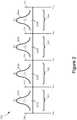
- FIG. 2is a diagram of voltage distributions 200 that may be found in a multi-level flash memory cell over time. Those skilled in the art will appreciate from the present disclosure that the voltage distributions 200 have been simplified for illustrative purposes.
- the cell voltage of a MLCapproximately extends from the voltage, V SS 210, at the source terminal of a NMOS transistor to the voltage, V DD 214, at the drain terminal.
- Sequential voltage ranges 201, 202, 203, 204 between the source and drain voltages, V SS 210 and V DD 214,are used to represent corresponding bit-tuples "11", “01”, “00", “10", respectively.
- Each voltage range 201, 202, 203, 204has a respective center voltage 201b, 202b, 203b, 204b.
- Each voltage range 201, 202, 203, 204also has a respective distribution of voltages 201a, 202a, 203a, 204a that may occur as a result of any number of a combination of factors, such as pseudo-random electrical fluctuations, defects in the storage medium, operating conditions, device history (e.g., large numbers of program-erase (P/E) cycles), and/or imperfect performance or design of write-read circuitry.
- P/Eprogram-erase
- the charge on the floating gate of the MLCwould be set such that the resultant cell voltage is at the center of one of the ranges 201, 202, 203, 204 in order to write the corresponding bit-tuple to the MLC.
- the resultant cell voltagewould be set to one of V 11 201b, V 10 202b, V 00 203b and V 10 204b in order to write a corresponding one of the bit-tuples "11", "01", "00” and "10.”
- the initial cell voltagemay differ from the center voltage for the data written to the MLC.
- Read comparison voltages V R1 211, V R2 212, and V R3 213are positioned between adjacent center voltages, e.g., positioned at or near the halfway point between adjacent center voltages, and thus define threshold voltages between the voltage ranges 201, 202, 203, 204.
- read comparison voltages V R1 211, V R2 212, and V R3 213are applied to determine the cell voltage using a comparison process.
- the actual cell voltage, and/or the cell voltage received when reading the MLCmay be different from the respective center voltage V 11 201b, V 10 202b, V 00 203b or V 10 204b corresponding to the data value written into the cell.
- the actual cell voltagemay be in an altogether different voltage range, strongly indicating that the MLC is storing a different bit-tuple than was written to the MLC. More commonly, the actual cell voltage may be close to one of the read comparison voltages, making it difficult to determine with certainty which of two adjacent bit-tuples is stored by the MLC.
- Errors in cell voltage, and/or the cell voltage received when reading the MLCcan occur during write operations, read operations, or due to "drive” of the cell voltage between the time data is written to the MLC and the time a read operation is performed to read the data stored in the MLC.
- cell voltage driftsometimes errors in cell voltage, and/or the cell voltage received when reading the MLC, are collectively called "cell voltage drift.”
- Grey-coding the bit-tuplesincludes constraining the assignment of bit-tuples such that a respective bit-tuple of a particular voltage range is different from a respective bit-tuple of an adjacent voltage range by only one bit. For example, as shown in Figure 2 , the corresponding bit-tuples for the adjacent ranges 201 and 202 are respectively "11" and "01", the corresponding bit-tuples for the adjacent ranges 202 and 203 are respectively "01” and "00”, and the corresponding bit-tuples for the adjacent ranges 203 and 204 are respectively "00" and "10".
- grey-codingif the cell voltage drifts close to a read comparison voltage level, the error is typically limited to a single bit within the 2-bit bit-tuple.
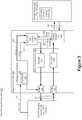
- Figure 3is a diagram of an implementation of a data storage environment 200 that utilizes information from the voltage distributions that occur in multi-level flash memory devices.
- the data storage environment 200 illustrated in Figure 3is similar to and adapted from the data storage environment 100 illustrated in Figure 1 .
- Elements common to eachinclude common reference numbers, and only the differences between Figures 1 and 3 are described herein for the sake of brevity.
- certain specific featuresare illustrated, those skilled in the art will appreciate from the present disclosure that various other features have not been illustrated for the sake of brevity and so as not to obscure more pertinent aspects of the example implementations disclosed herein.
- the data storage environment 200and in particular, the memory controller 120 has been further enabled to utilize soft information for decoding error control encoded data read from a storage medium 130 and, optionally, one or more of statistically determined read comparison signal values associated with one or more characteristics of the storage medium, and statistically determined shifted read comparison signal values associated with one or more characteristics of the storage medium and an identified error condition.
- the memory controller 120additionally includes a soft information generation module 229.
- the soft information generation module 229generates soft information values for each set of data read from storage medium 130 by utilizing a pre-generated collection of characterization vectors that includes soft information values for bit-tuples that may be read from the storage medium for various combinations of storage medium characterization parameter values.
- soft informationis generated by a device characterization process for memory devices produced by a particular manufacturing process, and stored in a characterization module or look-up table included in soft information generation module 229.
- Soft information generation module 229is coupled to management module 121, error control module 125 and storage medium I/O 128. More specifically, management module 121 is connected to provide soft information generation module 229 a control signal and one or more storage medium characterization parameter values on a control line 225 and a data line 226, respectively.
- Storage medium I/O 128is connected to receive read comparison voltages via data line 227, to be provided to storage medium 130 for use when reading data, and to provide soft information generation module 229 raw read data resulting from a read operation via data line 228.
- Soft information generation module 229is connected to provide decoder 127 with at least one sequence of soft information corresponding to the raw read data received from storage medium I/O 128.
- soft information generation module 229is also connected to provide storage medium I/O 128 with one or more sets of read comparison signal values (e.g., voltage levels or representations of voltage levels, etc.).
- management module 121includes soft information generation module 229.
- input buffer 123receives data to be stored in storage medium 130 from data processing system 110.
- the data in input buffer 123is made available to encoder 126, which encodes the data to produce a codeword.
- the codewordis conveyed to storage medium via storage medium I/O 128, which transfers the codeword to storage medium 130 in a manner dependent on the type of storage medium being utilized. For example, for MLC flash memory, each bit-tuple of the codeword is written into a respective memory cell by changing the charge on the floating gate of the respective memory cell.
- a read operationis initiated when the data processing system 110 (or the like) requests data from the storage medium 130 by sending a control signal on the control line 111 to the memory controller 120.
- the memory controller 120receives one or more storage medium characterization parameter values, associated with the current state of the storage medium 130, from the data processing system 110 along with the read request.
- the memory controller 120retrieves one or more storage medium characterization parameter values, associated with the current state of the storage medium 130, in response to receiving the read request from the data processing system 110.
- Management module 121 of memory control 120passes the read request to soft information generation module 229.
- the soft information generation module 229receives one or more storage medium characterization parameter values, associated with the current state of the storage medium 130, along with the read request. In some implementations, soft information generation module 229 retrieves the one or more storage medium characterization parameter values from one of management module 121, data processing system 110 and/or a storage medium characterization parameter value storage module in response receiving the read request.
- the one or more storage medium characterization parameter valuesprovide an indication of at least one of a physical characteristic associated with at least a portion the storage medium, a mode of operation associated with at least a portion of the storage medium, a history of use associated with at least a portion of the storage medium, a condition characteristic associated with at least a portion of the storage medium, a read type associated with at least a portion of the storage medium, and a location associated with at least a portion of the storage medium.
- the one or more storage medium characterization parameter valuesincludes an indicator of the storage medium locations being accessed, an indicator of the number of previous program/erase cycles of the storage medium locations being accessed, and an indicator of the current temperature of the storage medium 130.
- the soft information generation module 229retrieves a characterization vector based on the one or more storage medium characterization parameter values and prompts the storage medium I/O 128 to read from a portion of the storage medium 130, such as the selectable portion 131.
- the storage medium I/O 128reads from the storage medium and provides a sequence of raw hard-decision read data to the soft information generation module 229. It is worth noting that in some implementations the raw read data can be hard-decision data because the soft information stored in the characterization vectors in the characterization module is in many cases more statistically accurate than the raw electrical analog values read from individual memory cells for a given read operation.
- the soft information generation module 229can generate statistically accurate soft information values using a single-page read operation.
- the soft information generation module 229generates a sequence of soft information values corresponding to raw hard-decision read data by selecting a respective soft information value from the selected characterization vector for each bit-tuple in the raw hard-decision data read from the storage medium 130.
- the soft information generation module 229provides statistically determined read comparison signal values to the storage medium I/O 128.
- the statistically determined read comparison signal valuesare selected based on one or more storage medium characterization parameter values associated with the current state of the storage medium 130. As such, for a given current state of the storage medium 130, the statistically determined read comparison signal values may produce more accurate read data than a nominal design value chosen without regard to one or more storage medium characterization parameter values.
- the statistically determined read comparison signal valuesare stored in a collection of characterization vectors indexed by one or more storage medium characterization parameter values. As described in greater detail below with reference to Figures 4 and 10 , in some implementations, the statistically determined read comparison signal values are determined using a characterization process for devices produced by a particular manufacturing process.
- the soft information generation module 229provides statistically determined shifted read comparison signal values to the storage medium I/O 128.
- the statistically determined shifted read comparison signal valuesare offset relative to either a nominal design value or a first statistically determined read comparison signal value, and based on a set of transition probabilities determined using a characterization process for devices produced by a particular manufacturing process.
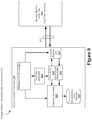
- FIG 4is a diagram of an implementation of the soft information generation module 229 included in Figure 3 .
- the soft information generation module 229includes a soft information management controller 410, a characterization module 420, a calculation/adjustment module 430, and an output multiplex (MUX) 440.
- soft information generation module 229is coupled to error control module 125, memory management module 120 and storage medium I/0 128.
- the soft information management controller 410is coupled to each of the characterization module 420, calculation/adjustment module 430, and MUX 440 in order to coordinate the operation of soft information generation module 229. More specifically, soft information management controller 410 is connected to receive a read request and one or more storage medium characterization parameters on control and data lines 401 and 402, respectively. Soft information management controller 410 is also connected to provide characterization module 420 a selection control signal on control line 411, and to receive a selected characterization vector on data line 412.
- soft information management controller 410is further connected to provide read comparison signal values (e.g., comparison voltages or another electrical signals) to the storage medium I/O 128 via data line 414, and receive raw read data from the storage medium I/O 128 via data line 415.
- Soft information management controller 410is also connected to provide sequences of soft information values to the calculation/adjustment module 430 and output MUX 440 via corresponding data lines 416 and 417, and a control signal to output MUX 440 via control line 403.
- Output MUX 440is also connected to receive an adjusted sequence of soft information values from calculation/adjustment module 430 on data line 431.
- Output MUX 440is connected to selectively provide soft information values from one of conversion module 433 and calculation/adjustment module 430 on data line 441 depending on the control signal received on control line 403.
- Characterization module 420includes a collection of characterization vectors 421-1, 421-2, 421-3,... 421-n, that each store characterization data, such as soft information values for bit-tuples and read comparison signal values, associated with storage medium 130 for one or more storage medium characterization parameter values.
- characterization datasuch as soft information values for bit-tuples and read comparison signal values
- the characterization data stored in the characterization vectors 421is statistically derived. More detailed example implementations of characterization vectors 421 are described below with reference to Figures 5A, 5B , 6A and 6B .
- Soft information management controller 410includes a selection module 431, a read controller 432, and a conversion module 433.
- the selection module 431is configured to use the one or more storage medium characterization parameters values to select a characterization vector from the stored collection of characterization vectors 421-1, 421-2, 421-3,... 421-n in accordance with the current state of storage medium 130.
- the selection control signalincludes one or more of storage medium characterization parameters values and/or an index key associated with a combination of one or more of storage medium characterization parameters values that enables characterization module 420 to select a characterization vector based on the one or more storage medium characterization parameters values associated with the current state of the storage medium 130.
- the read controller 432is configured to read a portion of the storage medium 130 via storage medium I/O 128. In some implementations, the read controller 432 is configured to provide storage medium I/O 128 with read comparison signal values for the read operation. In some implementations, for a first read, read controller 432 selects one or more statistically determined read comparison signal values from a characterization vector selected based on the one or more storage medium characterization parameter values associated with the current state of storage medium 130. In some implementations, read controller 432 is configured to read the same portion of the storage medium 130 a second time in response to a determination that the soft information values generated from the first read included an error that was uncorrectable by error control decoder 127.
- read controller 432selects one or more shifted read comparison signal values from the selected characterization vector.
- the shifted read comparison signal valuesindividually offset relative to a respective nominal or default read-signal value or a statistically determined first read comparison signal value based on set of transition probabilities, as discussed in greater detail below with reference to Figure 8 .
- the use of one or more shifted read comparison signal values during the second readproduces raw hard-decision read data read from storage medium 130 that is different from the raw hard-decision read data read as a result of the first read operation.
- Conversion module 433is configured to generate a sequence of soft information values corresponding to raw hard-decision read data.
- Calculation/adjustment module 430is configured to generate a third sequence of soft information values by combining the first and second sequences of soft information values.
- the third sequence of soft information valuesis generated in response to a determination that the second sequence of soft information values includes at least one uncorrectable error.
- the third sequence of soft information valuesis generated when the information from at least a portion of the second sequence of soft information values becomes available.
- each soft information value of the third sequence of soft information valuesis generated by comparing corresponding soft information values from the first and second sequences, and equating the respective one of the third sequence of soft information values to a first combination of the first and second soft information values when the comparison satisfies a first condition, and equating the respective one of the third sequence of soft information values to a second combination of the soft information values when the comparison satisfies a second condition.
- the two weighting factorsare pre-determined constants, while in other implementations they are generated based on the two sequences of LLRs, y LLR 1 and y LLR 2 .
- a first combination of the soft information valuescomprises only one of the first and second soft information values
- the second combination of the soft information valuescomprises a weighted combination of the first and second soft information values.
- the decoded databased on the final sequence of LLRs, y LLR f , is not tested to determine if the decoding was successful. Instead, without regard to any such determination, the resultant decoded data is sent to data processing system 110 ( Figure 1 , 3 ).
- the soft information provided by soft information generation module 229 in response to a read request from data processing system 110is limited to the first, second and third sequences of LLRs generated from two read operations.
- the maximum latencyEven if maximum latency is rarely encountered, data processing system 110 must be designed to accommodate the maximum latency of memory controller 120. Typically, shorter maximum latencies are preferred over longer maximum latencies.
- LLRscan be generated from transition probabilities, which are determined by statistically characterizing samples of memory devices, under various conditions, produced by a manufacturing process.
- Ybe the set of Q levels that a q -bit bit-tuple is read out from the flash memory cell based on read comparison voltages, such as the read comparison voltages V R1 V R2 and V R3 described above with reference to Figure 2 . Due to pseudo-random fluctuations, defects in the storage medium, operating conditions, device history, and/or write-read circuitry, etc., the read out voltage level from a flash memory cell y ⁇ Y may be different from the written voltage level x ⁇ X .
- the set of actual voltages for each level in memory celltypically has a distribution or set of possible values, as described above with reference to Figure 2 .
- the voltage distributionsare affected by factors such as page location, page type, program/erase (P/E) cycles, data mode (operation, retention), temperature, etc.
- the voltage distribution and the variation of the voltage distributionmay be used to generate soft information values, such as transition probabilities and/or LLRs, based on a device characterization process.
- q2 (i.e., 2 bits per cell in a MLC flash memory) to describe an implementation of a soft information generation method.
- 2-bit implementationmay be extended to other types of MLC flash memory that more bits ( q ⁇ 3) per memory cell.
- Each combination of storage medium characterization parameter valuesrepresents a respective state of a storage medium (e.g., flash memory device) that may be characterized in a device characterization process, and may exist for other devices produced by the same manufacturing process.
- a storage mediume.g., flash memory device
- datais written and read from the storage medium under test conditions that approximate each of characterization parameter value combinations, including various modes of operation (e.g., operation mode, retention mode, etc.).
- MLC flash memorye.g., storage media 130
- MLC flash memorythere are generally two types of read operations that may be performed on MLC flash memory that result in disjoint sets of transition probabilities.
- Oneis a single-page read, which includes reading the respective bits of a particular page from a number of q -page MLC flash memory cells.
- the two constituent pagesare referred to as the lower page and the upper page, where the lower page bit is typically the least significant bit of the 2-bit bit-tuple, and the upper page is the most significant bit.
- the single-page read scenarioone of the upper page and lower page bit from a number of MLC flash memory cells is read.
- a lower-page readdelivers a sequence of respective lower-page bits from a number of 2-page MLC flash memory cells.
- one or more transition probabilities tablesis generated by comparing write data and read data.
- Figure 5Ais a transition probability table 50 associated with either a SLC flash memory cell or a single-page read of a MLC flash memory cell for a particular combination of storage medium characterization parameter values.
- the transition probability values p 00 , p 10 , p 01 , p 11 in the transition probability table 50is determined as follows. Let x b and y b be the data bit written to a lower page and the data read from the same lower page, respectively.
- the transition probability p 00is the probability that a "0" was read when a "0" was written
- the transition probability p 01is the probability that a "1" was read when a "0” was written, etc.
- transition probabilities, and subsequently the LLRs, generated for a single-page readcorrespond to bit-tuples each including a single bit even though a MLC flash memory cell stores a bit-tuple including two or more bits.
- transition probability table for the upper pageis similarly obtained by writing and reading upper page data for a combination of storage medium characterization parameter values.
- Figure 6Ais a transition probability table 60 that is associated with a joint-page read of a MLC flash memory cell.
- a joint-page readgenerally includes reading the respective bits of two or more pages from a number of q -page MLC flash memory cells. Consequently, the sequence of read data includes multi-bit bit-tuples, and the transition probabilities and the LLRs generated for a joint-page read correspond to bit-tuples each including two or more bits. Accordingly, for a 2-page MLC flash memory the bits for both the upper page and lower page are read together, e.g., by determining the voltage level produced by a 2-bit flash memory cell during a read operation.
- the transition probability p 13is the probability that a "3" (or "11") was read when a "1" (or "01" was written. Further, as described above, for each write level the transition probabilities satisfy equation (4).
- transition probabilitiesmay be generated and stored in a collection of characterization vectors.
- the transition probabilitiesare stored in a collection of characterization vectors instead of, or in addition to, the LLRs.
- LLRsprovide a more compact representation of the soft information provided by the transition probabilities.
- y P x k1
- y krepresents the k -th bit read from a q-bit multi-level memory cell, which corresponds to a read out voltage level y ⁇ Y for 0 ⁇ k ⁇ q.
- x⁇ ⁇ ⁇ x k 1 P y
- x⁇
- equation (5a)simplifies to equations (6) and (7):
- x10
- P y11
- x01
- x00
- y11
- x10
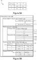
- Figure 5Bis a schematic diagram of an implementation of a characterization vector 500 (e.g., corresponding to any one of the characterization vectors 421 shown in Figure 4 ); in some implementations, characterization vector includes soft information values 532, 533 produced from transition probability values in table of Figure 5A .
- characterization vector 500includes a storage medium characterization parameters field 510, a read comparison voltages field 520, a single-page read LLR value field 530 and a weighting factors field 540.
- a characterization vectoris a data structure that facilitates reading raw data values from a storage medium and/or generating a sequence of soft information values corresponding to the read data.
- a memory controlleror a soft information generation module of a memory controller, generates a sequence of soft information values corresponding to raw read data by selecting a respective LLR value from a selected characterization vector for each bit-tuple of the read data.
- the raw read datais hard-decision data because pre-generated soft information, such as LLRs, may be more statistically accurate than the raw electrical values read from individual memory cells for a given read operation.
- the greater statistically accuracyis a result of a controlled device characterization process.
- the storage medium characterization parameters field 510is provided to store one or more storage medium characterization parameter values.
- the storage medium characterization parameters field 510includes a temperature field 511 and a P/E cycles field 512.
- a temperature field 511includes a temperature field 511 and a P/E cycles field 512.
- P/E cycles field 512includes a temperature field 511 and a P/E cycles field 512.
- any number of storage medium characterization parameter value fieldsmay be included in the storage medium characterization parameters field 510.
- the set of one or more storage medium characterization parameter valuesprovides an indication of at least one of a physical characteristic associated with at least a portion the storage medium, a mode of operation associated with at least a portion of the storage medium, a history of use associated with at least a portion of the storage medium, a condition characteristic associated with at least a portion of the storage medium, a read type associated with at least a portion of the storage medium, and a location associated with at least a portion of the storage medium.
- the storage medium characterization parameter values in field 510correspond to a state of the storage medium for which the remaining data in characterization vector 500 is applicable.
- a collection of characterization vectorsmay be indexed, and thus made searchable and selectable, by one or more storage medium characterization parameter values stored in the respective fields.
- characterization vector 500does not include storage medium characterization parameters field 510, and instead the storage medium characterization parameter values corresponding to characterization vector 500 are implied by the location of characterization vector 500 in a table or database of characterization vectors. For example, if there are three storage medium characterization parameters (a, b and c), having, 3, 4 and 5 potential values, respectively, there will a set of 60 (i.e., 3 x 4 x 5) distinct characterization vectors for 60 distinct states of the storage medium. Any one of the 60 characterization vectors is accessed by forming an index from the three storage medium characterization parameters (a, b and c) corresponding to the current state of the storage medium, and reading or otherwise obtaining the characterization vector corresponding to that index.
- the read comparison voltages field 520is provided to store read comparison voltages and/or indications of read comparison voltages applicable to a respective state of a storage medium characterized by the one or more storage medium characterization parameter values used to define characterization vector 500.
- the read comparison voltages field 520includes comparison voltages for different read operations.
- the read comparison voltages field 520includes a first read comparison voltages field 521 and a second read comparison voltages field 522.
- the first read comparison voltages in field 521are used during the first read of a set of flash memory cells.
- the first readis sometimes called the "normal read.”
- the first read comparison voltagesare default read comparison voltage values, such as default read comparison voltage values for devices produced using a particular manufacturing process.
- the first read comparison voltages field 521includes first statically determined read comparison voltage values, V R1-1 521a, V R2-1 521b and V R3-1 521c, which are generated by a characterization process for devices produced by a particular manufacturing process. For example, in some embodiments, the first read comparison voltage values are selected during a device characterization process to satisfy a respective threshold error rate.
- the second read comparison voltages field 522includes first statically determined shifted read comparison voltage values, V R1-2 522a, V R2-2 522b and V R3-2 522c, which are offset relative to a nominal read comparison signal value or the statistically determined first read comparison signal value based on set of transition probabilities, and used in response to an identified error condition.
- the read comparison voltages field 520includes actual read comparison voltage levels, such as read comparison voltages V R1 , V R2 and V R3 described above with reference to Figure 2 .
- the read comparison voltage field 520includes an indication of the read comparison voltages, such as an offset value, a percentage value and/or a discretized value.
- the single-page read LLR value field 530stores lower page LLR values 532 and upper page LLR values 533 for respective lower and upper page reads, which are indexed by read data values 531 (e.g., "0" and "1"). Sequences of soft information are generated from raw read data by selecting the appropriate LLR value for each bit-tuple in the read data. For example, for a lower page read, a respective one of the lower page LLR values 532 would be selected for each bit of raw data.
- first and second sequences of soft information valuesmay be combined to produce a third sequence of soft information values.
- the combination of the first and second sequences of soft information valuesutilizes weighting factors stored in characterization vector 500.
- the weighting factors field 540includes lower page weighting factors 541 for lower page reads and upper page weighting factors 542 for upper page reads.
- Figure 6Bis a schematic diagram of an implementation of a characterization vector 600 (e.g., corresponding to any one of the characterization vectors 421 shown in Figure. 4 ); in some implementations, characterization vector 600 includes soft information values 632, 633 produced from the transition probability values in table of Figure 6A .
- the characterization vector 600 illustrated in Figure 6Bis similar to characterization vector 500 illustrated in Figure 5B .
- Elements common to both characterization vectorshave been assigned the same reference numbers, and only the differences between the characterization vectors 500 and 600, shown in Figures 5B and 6B , are described herein for the sake of brevity.
- certain specific featuresare illustrated, those skilled in the art will appreciate from the present disclosure that various other features have not been illustrated for the sake of brevity and so as not to obscure more pertinent aspects of the example implementations disclosed herein.
- characterization vector 600includes a joint-page read LLR value field 630 that stores lower page LLR values 632 and upper page LLR values 633 for respective lower and upper page reads, which are indexed by read data values 631. As described above, sequences of soft information are generated from raw read data by selecting the appropriate pair of LLR values for each bit-tuple in the read data. Additionally, in some implementations, the weighting factor field 640 stores weighting factors 641a, 641b applicable to both lower page and upper page reads.
- Figure 7is a flowchart representation of a method 700 of generating soft information values from data read from a storage medium.
- method 700is performed by a memory controller or a module associated with a memory controller.
- method 700includes reading data from a storage medium using one or more read comparison signal values, selected based on the current state of the storage medium, generating a corresponding sequence of soft information values from the read data and the current state of the storage medium, and determining whether to produce one or more additional sequences of soft information values.
- the read comparison signal value(s) and soft information values for various bit-tuplesare stored in characterization vectors that are selectable based on one or more storage medium characterization parameter values.
- sequences of soft information values generated from raw read dataare based on one or more storage medium characterization parameter values associated with the current state of the storage medium (e.g., a flash memory).
- method 700includes receiving a read data request.
- the memory controller 120receives a read data request from data processing system 110, and passes the request to soft information generation module 229.
- method 700includes receiving or retrieving one or more storage medium characterization parameter values associated with a current state of the storage medium.
- one or more of the storage medium characterization parameter valuesare received with the read data request.
- one or more of the storage medium characterization parameter valuesare retrieved in response to receiving the read data request.
- method 700includes using the one or more one or more storage medium characterization parameter values to retrieve a characterization vector (e.g., vector 421, 500 or 600, shown in Figures 4 , 5B or 6B , respectively).
- a characterization vectore.g., vector 421, 500 or 600, shown in Figures 4 , 5B or 6B , respectively.
- the soft information management controller 410uses the one or more storage medium characterization parameter values to transmit a selection control signal on control line 411 to characterization module 420.
- the characterization module 420provides at least a portion of a characterization vector (corresponding to the one or more storage medium characterization parameter values) to the soft information management controller 410 via data line 412.
- method 700includes selecting one or more first read comparison voltages from the selected characterization vector.
- method 700includes providing the selected one or more first read comparison voltages (as well as an address or other location value) to the read circuitry (e.g., storage medium I/O 128) and receiving raw read data (e.g., a codeword) from storage medium 130.
- method 700includes generating a first sequence of soft information values by assigning at least one soft information value from the characterization vector (retrieved at 7-3) to each bit-tuple in the raw read data from the first read.
- method 700includes providing the raw read data (e.g., a codeword) read from storage medium 130 and the corresponding first sequence of soft information values to an ECC decoder (e.g., decoder 127, Figure 3 ).
- ECC decodere.g., decoder 127, Figure 3
- method 700includes determining whether the ECC decoder successfully decoded the codeword using the first sequence of soft information values. If the decoding is successful ("Yes" path from block 7-8), as represented by block 7-9, method 700 ends for the codeword corresponding to the first sequence of soft information values because no further action is required to read the associated data successfully. On the other hand, if the decoding is not successful ("No" path from block 7-8), as represented by block 7-10, method 700 includes receiving an error indicator.
- method 700includes selecting one or more second read comparison voltages from the previously selected characterization vector.
- method 700includes providing the selected one or more second read comparison voltages to the read circuitry (e.g., storage medium I/O 128) and receiving a new set of raw read data from storage medium 130.
- method 700includes generating a second sequence of soft information values by assigning at least one soft information value from the characterization vector to each bit-tuple in the raw read data from the second read.
- method 700includes providing the second sequence of soft information values to an ECC decoder (e.g., decoder 127, Figure 3 ).
- ECC decodere.g., decoder 127, Figure 3
- method 700includes determining whether the ECC decoder successfully decoded the codeword (obtained from the second read) using the second sequence of soft information values. If the decoding is successful ("Yes" path from block 7-15), as represented by block 7-9, method 700 ends for the codeword from the second read because no further action is required to read the associated data successfully.
- method 700includes generating a third sequence of soft information values by combining the first and second sequences of soft information values as describe above with reference to equations (1) and (2), and further described below with reference to Figure 8 .
- Figure 8is a flowchart representation of an implementation of a method 800 of generating soft information values from previously generated soft information values.
- method 800is performed by a memory controller or a module associated with a memory controller.
- method 800includes generating a third sequence of soft information values based on a combination of two previously generated sequences of soft information values.
- method 800includes selecting a soft information value from the first sequence of soft information values previously generated, and as represented by block 8-2, selecting a corresponding soft information value from the second sequence of soft information values previously generated.
- method 800includes determining whether the signs (i.e., positive or negative) of the selected soft information values from the first and second sequences match. If the signs match (e.g., both are positive or both are negative numbers), as represented by block 8-5, method 800 includes setting or equating the respective soft information value of the third sequence to the soft information value selected from only the second sequence of soft information values ("Yes" path from block 8-5). On the other hand, if the signs do not match, as represented by block 8-4 and with reference to equations (1), (2) and (3), method 800 includes setting or equating the respective soft information value of the third sequence to a weighted combination of values selected from the first and second sequences of soft information values.
- Figure 9is a diagram of an implementation of a storage medium characterization environment 900 operable to generate soft information values and statistically determined read comparison signal values for a storage medium, such as a MLC flash memory. While certain specific features are illustrated, those skilled in the art will appreciate from the present disclosure that various other features have not been illustrated for the sake of brevity and so as not to obscure more pertinent aspects of the example implementations disclosed herein. To that end, as a non-limiting example, the characterization environment 900 includes a storage medium under test 930 and a characterization controller 920.
- the storage medium under test 930includes one or more memory devices (e.g., MLC flash memory devices) produced by the same manufacturing process.
- the characterization controller 920includes a management module 921, a test data generator 923, a statistics generator 926, a storage medium I/O 928, a write buffer 924, a read buffer 925, and a characterization vector database 929.
- characterization controller 920includes one or more processors (not shown) for executing one or more programs, including management module 921, test data generator 923, and statistics generator 926.
- management module 921, test data generator 923, and statistics generator 926are programs stored in a non-volatile computer readable storage medium (not shown), such as one or more DRAM devices and/or non-volatile memory devices, and the non-volatile computer readable storage medium is coupled to the one or more processors by one of more communication busses (not shown).
- Management module 921is coupled to statistics generator 926, test data generator 923 and storage medium I/O 128 in order to coordinate operation of the characterization controller 920.
- Storage medium I/O 928provides an interface to the storage medium under test 930 though data connections 903.
- storage medium I/O 928includes read and write circuitry, including circuitry capable of providing read comparison signal values, such as voltages, to signal lines coupled to the storage medium under test 930.
- Write buffer 924 and read buffer 923are coupled in parallel between I/O 928 and statistics generator 926.
- Write buffer 924 and read buffer 923are readable by statistics generator 926.
- Write buffer 924is readable by the storage medium I/O 928, and read buffer 923 is writable by storage medium I/O 928. Additionally, write buffer 924 is writable by test data generator 923.
- Statistics generator 926is capable of writing characterization vectors to characterization vector database 929.
- test data generator 924provides write data to the write buffer 924.
- the storage medium I/O 928writes the data in the write buffer 924 to the storage medium under test 930.
- storage medium I/O 928reads the data from the storage medium under test 930 and provides the read data to read buffer 923.
- the statistics generator 926compares the contents of write buffer 924 and read buffer 923 to determine the presence and location of errors in the read data.
- the processis repeated multiple times, within the bounds of the one or more storage medium characterization parameter values corresponding to a characterization vector, in order to produce a statistically significant amount of test data from which transition probability values, LLR values and statistically based read comparison voltages can be calculated for inclusion the characterization vector.
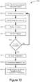
- Figure 10is a flowchart representation of a method 1000 of generating one or more characterization vectors, including soft information values and read comparison voltages based on characterization data, in accordance with some embodiments.
- method 1000is performed by a module associated with a memory controller.
- method 1000includes statistically characterizing memory devices produced by a particular manufacturing process.
- method 1000includes selecting a set (sometimes herein called the specified set) of one or more storage medium characterization parameter values in order to define testing conditions for a characterization vector.
- method 1000includes generating data vectors (i.e., test data). In some implementations, the data vectors are pseudo-randomly generated.
- method 1000includes writing and reading the data vectors.
- method 1000includes recording the presence and location of errors in the read data vectors and generating statistics associated with the presence and location of errors in the read data vectors.
- method 1000includes recording the raw read voltage values, corresponding to the stored data vectors after a write and read.
- method 1000includes determining if sufficient data has been collected for the storage medium with respect to the specified set of storage medium characterization parameters values, in which case the testing for the specified set of storage medium characterization parameters is complete.
- testingis complete when the collected information satisfies a predetermined level of statistical accuracy.
- testing completionfurther requires that the collected information be sufficient to generate first read comparison voltage values that satisfy a respective threshold error rate.
- testing completionrequires that the collected information be sufficient to generate transition probability values having a predetermined level of statistical accuracy.
- method 1000includes repeating the portions of method 1000 represented by blocks 10-2 to 10-5 in order to generate more test data.
- method 1000includes generating transition probabilities for the characterization vector (i.e., the characterization vector corresponding to the specified set of one or more storage medium characterization parameter values).
- method 1000includes converting the transition probabilities to LLR values.
- method 1000includes generating distributions of the recorded read voltages (which are optionally generated while the reading voltages are recorded), and identifying respective voltages troughs from the distributions of recorded read voltages to use as first read comparison voltage values.
- the read comparison voltages V R1 211, V R2 212, and V R3 213are in voltage troughs positioned between adjacent center voltages, and define threshold voltages between the voltage ranges 201, 202, 203, 204.
- method 1000bases the selection of a read comparison voltage on whether each such read comparison voltage is in the trough between two voltage distributions, in addition to or as an alternative to spacing the read comparison voltages at or near the halfway point between a respective pair of center voltages.
- method 1000selects the read comparison voltages in accordance with predefined error minimization criteria (e.g., by selecting read comparison voltages that minimize read errors, in accordance with the recorded information).
- predefined error minimization criteriae.g., by selecting read comparison voltages that minimize read errors, in accordance with the recorded information.
- method 1000selects read comparison voltages that satisfy a respective (e.g., predefined) threshold error rate.
- the generated distributions of recorded read voltagesare sometimes herein called statistics.
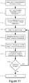
- Figure 11is a flowchart representation of a method 1100 of generating shifted read comparison signal values (e.g., voltages) for reading data from multi-level memory cells, based on transition probabilities,
- method 1100is performed by a module associated with a memory controller.
- method 1100includes statistically characterizing memory devices produced by a particular manufacturing process in order to determine a second set of read comparison signal values that may be used if a first set of read comparison signal values fails to provide data without at least one uncorrectable error.
- method 1100includes selecting a set of one or more storage medium characterization parameter values (sometimes herein called the specified set) defining testing conditions for a characterization vector.
- method 1100includes generating transition probabilities for the specified set of one or more storage medium characterization parameter values. For example, the transition probabilities may be generated using the method described above with reference to Figure 10 .
- method 1100includes retrieving or selecting the respective voltages troughs to use as first set of read comparison voltage values. Additionally and/or alternatively, the first set of read comparison voltage values may be nominal values based on equally spacing read comparison voltage values across the voltage range of a memory cell.
- method 1100includes selecting one of the voltage troughs for which method 1100 will generate a corresponding shifted read comparison voltage value for the second set of read comparison voltage values to be stored in the characterization vector (i.e., the characterization vector corresponding to the specified set of one or more storage medium characterization parameter values).
- method 1100includes determining the offset direction of the respective shifted read comparison voltage in relation to the selected voltage trough, based on transition probabilities, In some implementations, determining the offset direction includes determining the sign of the difference between two transition probabilities representing adjacent voltage levels within a MLC flash memory cell. For example, with further reference to Figures 2 and 6A , as described above, one way to reduce the impact of a cell voltage drifting from one voltage range to an adjacent voltage range is to grey-code the bit-tuples. Grey-coding the bit-tuples includes constraining the assignment of bit-tuples such that a respective bit-tuple of a particular voltage range is different from a respective bit-tuple of an adjacent voltage range by only one bit.
- the corresponding bit-tuples for the adjacent ranges 201 and 202are respectively "11" and “01”
- the corresponding bit-tuples for the adjacent ranges 202 and 203are respectively “01” and "00”
- the corresponding bit-tuples for the adjacent ranges 203 and 204are respectively "00" and "10”.
- grey-codingallows the transition probabilities to be used to generate a second or fallback (i.e., shifted) read comparison voltage value that may be used if the first read comparison voltage fails to produce a desired result.
- grey-codinggenerally restricts the most-likely errors of multi-bit bit-tuples to single-bit errors.
- pairs of transition probabilities associated with such errorsare positioned adjacent along (i.e., adjacent, but not on) the diagonal of table 60 in Figure 6A .
- the transition probability pair( p 31 , p 13 ) is used to generate the direction of a respective shifted read comparison voltage value offset from the read comparison voltage value V R1 .
- the direction of the offset from the read comparison voltage value V R1is provided by the sign of the difference of ( p 31 - p 13 ).
- transition probability pairs ( p 10 , p 01 ) and ( p 02 , p 20 )are be used to generate the respective directions of respective shifted read comparison voltage values offset from corresponding read comparison voltage values V R2 , V R3 , respectively.
- method 1100includes determining the magnitude of the offset of the shifted read comparison voltage, in relation to the selected read comparison voltage, based on the transition probabilities.
- the magnitude of the offsetis based on the same two transition probabilities, ( p ij , p ji ) , used to determine the direction of the aforementioned offset.
- the magnitude of the offset from the read comparison voltage value V R1is determined as a function of the transition probability pair ( p 31 , p 13 ) .
- the magnitude of the offsetis determined as the absolute value of the difference between the probabilities of a transition probability pair (e.g., ( p 31 , p 13 )) , In other words, the magnitude of the offset tracks the absolute value (e.g.,
- the magnitude of the offsetis determined as a linear or non-linear function of the absolute value of the difference between the probabilities of a transition probability pair, ( p ij , p ji ). In some implementations, the magnitude of the offset is a linear function of the difference between the respective transition probability pair, ( p ij , p ji ). For example, in some implementations, the magnitude of the offset is linearly determined as ⁇ ⁇
- ⁇is determined by manufacturing process characterization data.
- the magnitude of the offsetis a non-linear function of the difference between the respective transition probability pair, ( p ij , p ji ).
- the magnitude of the offsetis non-linearly determined as ⁇ ⁇
- the non-linear characterizations, represented by ⁇are determined from at least one of flash characterization data and manufacturing process characterization data.
- a curve fitting processis used in combination with one or more types of characterization data (e.g., flash characterization data, manufacturing process characterization data, etc.) to produce a higher-order non-linear model that can be used to determine the magnitude of the offset from a given probability pair ( p ij , p ji ),
- a respective mathematical modelincludes multiple terms, each having a respective scaling coefficient and/or exponent value.
- a curve fitting processis used to determine one or more coefficients and/or one or more exponent values of the non-linear model.
- the offset equations (or model)are determining using a machine learning methodology. For example, the equations are formulated using a combination of read out data and previously determined information, such as flash characterization data and and/or data patterns based on historical data.
- method 1100includes storing the shifted read comparison voltage (or the offset between the shifted read comparison voltage and the corresponding read comparison voltage) in the characterization vector. As represented by block 11-8, method 1100 includes determining whether there are additional read comparison voltage levels to consider. If there are additional read comparison voltage levels to consider ("Yes" path from block 11-8), method 1100 includes repeating the portion of the method represented by blocks 11-4 to 11-7 so as determine an additional shifted read comparison voltage to be stored in the characterization vector for the specified set of one or more storage medium characterization parameter values. On the other hand, if there are no other read comparison voltage levels to consider ("No" path from block 11-8), method 1100 stops for the specified set of one or more storage medium characterization parameter values, as represented by block 11-9.
- Figure 12is a flowchart representation of an implementation of a method 1200 of reading data from a storage medium, using multiple sets of read comparison voltages stored in a characterization vector for the storage medium.
- method 1200is performed by a memory controller or a module associated with a memory controller that is coupled to the storage medium, and is typically performed when a first read operation (see blocks 12-3, 12-4 and 12-5) fails to obtain data having no unrecoverable errors.
- method 1200includes retrieving at least two read comparison voltages from the characterization vector corresponding to a specified set of one or more storage medium characterization parameter values (e.g., corresponding to the current state of a storage medium), and applying the at least two read comparison voltages to read circuitry so as to retrieve raw data from the same set of memory locations of the storage medium at two different times.
- method 1200includes receiving or retrieving a specified set of one or more storage medium characterization parameter values corresponding to a current state of the storage medium from which data is to be read.
- method 1200includes selecting a characterization vector based on the specified set of storage medium characterization parameter values.
- method 1200includes obtaining the first read comparison voltage values from the selected characterization vector.
- method 1200includes providing the first read comparison voltage values to read circuitry of the storage medium from which data is to be read.
- method 1200includes receiving first read data values, from one or more specified addresses or memory locations of the storage medium, based on the first read comparison voltage values.
- method 1200further includes obtaining the second read comparison voltage values from the selected characterization vector. As represented by block 12-7, method 1200 includes providing the second read comparison voltage values to read circuitry of the storage medium. As represented by block 12-8, method 1200 includes receiving second read data values from the same one or more specified addresses or memory locations of the storage medium as those accessed in block 12-5, based on the second read comparison voltage values. As described above, but not shown in Figure 12 , in some implementations data values for the one or more specified addresses or memory locations of the storage medium is recovered using at least the second read data values.
- firstmeans "first,” “second,” etc.
- these elementsshould not be limited by these terms. These terms are only used to distinguish one element from another.
- a first contactcould be termed a second contact, and, similarly, a second contact could be termed a first contact, which changing the meaning of the description, so long as all occurrences of the "first contact” are renamed consistently and all occurrences of the second contact are renamed consistently.
- the first contact and the second contactare both contacts, but they are not the same contact.
- the phrase “if it is determined [that a stated condition precedent is true]” or “if [a stated condition precedent is true]” or “when [a stated condition precedent is true]”may be construed to mean “upon determining” or “in response to determining” or “in accordance with a determination” or “upon detecting” or “in response to detecting” that the stated condition precedent is true, depending on the context.
Landscapes
- Engineering & Computer Science (AREA)
- Theoretical Computer Science (AREA)
- Quality & Reliability (AREA)
- Physics & Mathematics (AREA)
- General Engineering & Computer Science (AREA)
- General Physics & Mathematics (AREA)
- Computer Hardware Design (AREA)
- Techniques For Improving Reliability Of Storages (AREA)
- Read Only Memory (AREA)
- For Increasing The Reliability Of Semiconductor Memories (AREA)
Description
- This application claims the benefit of
U.S. Provisional Patent Application No. 61/556,793, filed on November 7, 2011 - The present disclosure relates to using error control in memory systems, and in particular, to generating and using soft information for decoding data read from a memory.
- The ever-present demand for the continual enrichment of consumer electronics and enterprise computing systems is often accompanied by demand to improve data storage capacity. The demand for greater storage capacity in turn stokes demand for greater storage density, so that specifications such as power consumption and form factor may be maintained and preferably reduced. Non-volatile memories, and flash memory in particular, are becoming increasing popular because they have enabled increased portability of consumer electronics, and more recently, have been utilized in relatively low power enterprise mass storage systems suitable for cloud computing and other mass storage applications. As such, there is additional pressure to increase the storage density of non-volatile memories, such as flash memory, in order to further take advantage of the beneficial attributes of such devices.
- Semiconductor memory devices, including flash memory, typically utilize memory cells to store data as an electrical value, such as an electrical charge or voltage. A flash memory cell, for example, includes a single transistor with a floating gate that is used to store a charge representative of a data value. Increases in storage density have been facilitated in various ways, including reducing the minimum feature size of semiconductor manufacturing processes in order to increase the number of transistors - and thus memory cells - that can be included in a particular area. Additionally, in order to further increase storage density, flash memory has developed from single-level flash memory to multi-level flash memory so that two or more bits can be stored by each memory cell.
- A drawback of increasing storage density is that the stored data is increasingly prone to being stored and/or read erroneously. Error control coding ("ECC") has been utilized to limit the number of uncorrectable errors that are introduced by pseudo-random fluctuations, defects in the storage medium, operating conditions, device history, and/or write-read circuitry, etc. Error control methods using soft information are particularly promising because soft information decoding may improve the error detection and correction capability of a particular error control code, and thus the capacity of the system. However, the utilization of soft information decoding has been limited because of a number of previously irresolvable drawbacks. For example, soft information decoding implementations tend to introduce undesirable delays, are generally power intensive and have relatively large semiconductor footprints. Consequently, the soft information decoding methods have remained relatively undesirable due to these and other physical constraints.
US 2011/205823 provides non-volatile storage with temperature compensation based on Neighbour State Information. - The present invention provides a method of generating soft information values for bit-tuple data values read from a storage medium, as claimed in
claim 1. The present invention also provides a device operable to generate soft information values for bit-tuple data values read from a storage medium, as claimed inclaim 11. After considering this disclosure, and particularly after considering the section entitled "Detailed Description" one will understand how the features of various implementations are used to enable: (i) generating and utilizing soft information for decoding error control encoded data read from a storage medium; (ii) determining and utilizing statistically determined read comparison signal values associated with one or more storage medium characteristics; and, (iii) determining and utilizing statistically determined shifted read comparison signal values associated with one or more storage medium characteristics. - Some implementations include systems, methods and/or devices enabled to utilize soft information error correction decoding to support the use of flash memory or other storage mediums. More specifically, in some implementations, a soft information generation system, method and/or device utilizes a pre-generated collection of characterization vectors, for corresponding sets of storage medium characterization parameter values, that includes soft information values for bit-tuples that may be read from the storage medium. In some implementations, the soft information is generated by a device characterization process for memory devices produced by a particular manufacturing process, and stored in a characterization module or look-up table. The characterization module or look-up table is indexed using storage medium characterization parameter values.During a read operation, soft information is generated by retrieving a particular characterization vector from the characterization module based on one or more storage medium characterization parameter values associated with the current state of the storage medium, and selecting a respective soft information value from the selected characterization vector for each bit-tuple in the raw data read from the storage medium.
- Some implementations include systems, methods and/or devices enabled to generate soft information, in the form of log-likelihood ratios (LLR) and/or transition probabilities, from characterization vectors including soft information values for bit-tuples associated with at least one of singe-page reads and joint-page reads for multi-level flash memory devices. The soft information values may then be passed to an ECC decoder, such as a low density-parity check (LDPC) code decoder or any of a number of other error correction code decoders. Some implementations utilize statistical data from a device characterization process to generate the collection of characterization vectors for a number of combinations of device conditions and process variations indexed by one or more storage medium characterization parameter values. In some implementations, the characterization vectors each include soft information values (e.g., LLR values and/or transition probabilities). In some implementations the characterization vectors each include at least one set of read comparison signal values (e.g., voltages) determined from the statistical data of the device characterization process. In some implementations, the characterization vectors each include two sets of read comparison signal values, determined from the statistical data of the device characterization process. The second set of read comparison signal values is shifted from the first set of read comparison signal values as a function of transition probabilities derived from the device characterization process.
- Some implementations enable the combination of two previously generated sequences of soft information values to produce a third sequence of soft information values, in order to limit the number of read operations used to provide error corrected data from a particular set of data locations in the storage medium. To that end, in some implementations, at least one of the characterization vectors (or, alternatively, each of the characterization vectors) include a set of weighting factors that can be used to generate the third sequence of soft information values from two previously generated sequences of soft information values. Some implementations dynamically calculate the weighting factors based on one or more current storage medium characteristics. Additionally and/or alternatively, in some implementations, the third sequence of soft information values is generated in response to an identified error condition.
- In some implementations, the total latency associated with reading data can be controlled by limiting the number of read operations (e.g., at most two read operations). Moreover, in some implementations, the soft information values that are generated may be more reliable than the soft information values used in previous methods because one or more of the read comparison signal values and the soft information values for particular bit-tuples are based on one or more storage medium characterization parameters values, such as an indication of at least one of a physical characteristic associated with at least a portion the storage medium, a mode of operation associated with at least a portion of the storage medium, a history of use associated with at least a portion of the storage medium, a condition characteristic associated with at least a portion of the storage medium, a read type associated with at least a portion of the storage medium, and a location associated with at least a portion of the storage medium.
- Some implementations include systems, methods and/or devices enabled to read data from a storage medium using a statistically determined read comparison signal value, selected based on a set of one or more storage medium characterization parameter values associated with the current state of the storage medium. In some implementations, the statistically determined read comparison signal values are stored in a collection of characterization vectors, and are generated by a characterization process for devices produced by a particular manufacturing process.
- Some implementations include systems, methods and/or devices enabled to read data from a storage medium using a statistically determined shifted read comparison signal value, which is offset relative to a nominal read comparison signal value or a statistically determined first read comparison signal value based on transition probabilities, and used in response to an identified error condition. In some implementations, the statistically determined shifted read comparison signal value is selected based on a set of one or more storage medium characterization parameter values associated with the current state of the storage medium. In some implementations, the various shifted read comparison signal values are stored in a collection of characterization vectors, and are generated by a characterization process for devices produced by a particular manufacturing process.
- So that the present disclosure can be understood in greater detail, a more particular description may be had by reference to the features of various implementations, some of which are illustrated in the appended drawings. The appended drawings, however, merely illustrate the more pertinent features of the present disclosure and are therefore not to be considered limiting, for the description may admit to other effective features.
Figure 1 is a diagram of an implementation of a data storage environment.Figure 2 is a diagram of voltage distributions that may be found in a multi-level flash memory cell over time.Figure 3 is a diagram of an implementation of a data storage environment, including a soft information generation module.Figure 4 is a diagram of an implementation of the soft information generation module included inFigure 3 .Figure 5A is a transition probability table that may be associated with either a single-level memory cell or a single-page read of a multi-level memory cell.Figure 5B is a schematic diagram of an implementation of a characterization vector that may be produced from the transition probability table ofFigure 5A .Figure 6A is a transition probability table that may be associated with a joint-page read of a multi-level memory cell.Figure 6B is a schematic diagram of an implementation of a characterization vector that may be produced from the transition probability table ofFigure 6A .Figure 7 is a flowchart representation of an implementation of a method of generating soft information values from data read from a storage medium.Figure 8 is a flowchart representation of an implementation of a method of generating soft information values from previously generated soft information values.Figure 9 is a diagram of an implementation of a characterization environment operable to generate soft information values and read comparison voltages for a storage medium.Figure 10 is a flowchart representation of an implementation of a method of generating one or more characterization vectors.Figure 11 is a flowchart representation of an implementation of a method of generating shifted read comparison voltages for reading from multi-level memory cells.Figure 12 is a flowchart representation of an implementation of a method of using multiple sets of read comparison voltages stored in a characterization vector.- In accordance with common practice the various features illustrated in the drawings may not be drawn to scale. Accordingly, the dimensions of the various features may be arbitrarily expanded or reduced for clarity. In addition, some of the drawings may not depict all of the components of a given system, method or device. Finally, like reference numerals may be used to denote like features throughout the specification and figures.
- The various arrangements and embodiments described herein include systems, methods and/or devices that may enhance the performance of error control codes used to improve the reliability with which data can be stored and read in a memory. Some implementations include systems, methods and/or devices to generate and utilize soft information for decoding error control encoded data read from a storage medium. More specifically, embodiments of the invention utilize a collection of characterization vectors that include soft information values for bit-tuples that may be read from the storage medium, each characterization vector corresponding to a different set of storage medium characterization parameter values associated with the current state of the storage medium. Additionally, some embodiments are enabled to determine and utilize read comparison signal values, identified from corresponding sets of statistical distributions associated with one or more storage medium characterization parameter values, in order to produce a first sequence of soft information values. Additionally, some embodiments are enabled to determine and utilize shifted read comparison signal values associated with one or more storage medium characterization parameter values and an identified error condition, in order to produce a second sequence of soft information values. Additionally, some embodiments are enabled to combine the first and second sequences of soft information values to produce a third sequence of soft information values in response to an identified error condition.
- Numerous details are described herein in order to provide a thorough understanding of the example implementations illustrated in the accompanying drawings. However, the invention may be practiced without many of the specific details. And, well-known methods, components, and circuits have not been described in exhaustive detail so as not to unnecessarily obscure more pertinent aspects of the implementations described herein.
Figure 1 is a diagram of an implementation of adata storage environment 100. While some example features are illustrated, those skilled in the art will appreciate from the present disclosure that various other features have not been illustrated for the sake of brevity and so as not to obscure more pertinent aspects of the example implementations disclosed herein. To that end, as a non-limiting example, thedata storage environment 100 includes adata processing system 110, amemory controller 120, and astorage medium 130. In some implementations,storage medium 130 comprises one or more flash memory devices. In some implementations,storage medium 130 comprises at least one of NAND-type flash memory and NOR-type flash memory.- The
data processing system 110 is coupled to thememory controller 120 throughdata connections 101. Moreover, those skilled in the art will appreciate from the present disclosure that in various implementations thedata processing system 110 includes thememory controller 120 as a component. Thedata processing system 110 may be any suitable computer device, such as a computer, a laptop computer, a tablet device, a netbook, an internet kiosk, a personal digital assistant, a mobile phone, a smart phone, a gaming device, a computer server, or any other computing device. In some implementations, thedata processing system 110 includes one or more processors, one or more types of memory, a display and/or other user interface components such as a keyboard, a touch screen display, a mouse, a track-pad, a digital camera and/or any number of supplemental devices to add functionality. - The
storage medium 130 is coupled to thememory controller 120 throughdata connections 103. Moreover, those skilled in the art will appreciate from the present disclosure that in various implementations thememory controller 120 andstorage medium 130 are included in the same device as constituent components thereof. Thestorage media 130 may include any number (i.e., one or more) of memory devices including, without limitation, non-volatile semiconductor memory devices, such as flash memory. For example flash memory devices can be configured for enterprise storage suitable for applications such as cloud computing. Additionally and/or alternatively, flash memory can also be configured for relatively smaller-scale applications such as personal flash drives or hard-disk replacements for personal, laptop and tablet computers. - Storage mediums are often divided into a number of addressable and individually selectable blocks, such as
selectable portion 131. In some embodiments, for flash memory, the individually selectable blocks are the minimum size erasable units in a flash memory device. In other words, each block contains a minimum number of memory cells that can be erased simultaneously. Each block is usually further divided into a plurality of pages, where each page is typically an instance of a minimum unit the smallest individually accessible sub-block in the block. However, a minimum unit of a data set may also be a sector in some types of flash memory. That is, each page contains a plurality of sectors and each sector is a minimum unit of the data set such that a page is the minimum unit for data writing or reading to the flash memory device. - Generally, one block may comprise any number of pages, for example, 64 pages, 128 pages, 256 pages, or another suitable number of pages. Blocks are typically grouped into a plurality of zones. Each block zone can be independently managed to some extent, which increases the degree of parallelism of parallel operations and simplifies management of
storage medium 130. - As noted above, while data storage densities of non-volatile semiconductor memory devices are generally increasing, a drawback of increasing storage density is that the stored data is increasingly prone to being stored and/or read erroneously. As described in greater detail below, error control coding can be utilized to limit the number of uncorrectable errors that are introduced by pseudo-random fluctuations, defects in the storage medium, operating conditions, device history, write-read circuitry, etc., or a combination of such factors.
- In some implementations,
memory controller 120 includes amanagement module 121, aninput buffer 123, anoutput buffer 124, anerror control module 125 and a storage medium interface (I/O) 128. Those skilled in the art will appreciate from the present disclosure thatmemory controller 120 may include various additional features that have not been illustrated for the sake of brevity and so as not to obscure more pertinent features of the example implementations disclosed herein, and that a different arrangement of features may be possible. The input and output buffers 123,124 provide an interface to thedata processing system 110 through thedata connections 101. Similarly, storage medium I/O 128 provides an interface tostorage medium 130 thoughdata connections 103. In some implementations, storage medium I/O 128 includes read and write circuitry, including circuitry capable of providing read comparison signal values tostorage medium 130. - In some implementations,
management module 121 includes aprocessor 122 configured to execute instructions in one or more programs, e.g., inmanagement module 121. However, those skilled in the art will appreciate from the present disclosure thatprocessor 122 may be shared by one or more components within, and in some cases, beyond the function ofmemory controller 120.Management module 121 is coupled to the input andoutput buffers error control module 125 and storage medium I/O 128 in order to coordinate the operation of these components. Error control module 125 is coupled between the storage medium I/O 128 and the input andoutput buffers error control module 125 is provided to limit the number of uncorrectable errors inadvertently introduced into data. To that end, theerror control module 125 includes anencoder 126 and adecoder 127. Theencoder 126 encodes data by applying an error control code to produce a codeword which is subsequently stored instorage medium 130. When the encoded data is read from the storage medium,decoder 127 applies a decoding process to recover the data, and to correct errors in the recovered data within the error correcting capability of the error control code. Those skilled in the art will appreciate from the present disclosure that various error control codes have different error detection and correction capacities, and that particular codes are selected for various applications for reasons beyond the necessary scope of this disclosure. As such, an exhaustive review of the various types of error control codes has not been provided for the sake of brevity. Moreover, those skilled in the art will appreciate that each type or family of error control codes may have encoding and decoding algorithms that are particular to the type or family of error control codes. On the other hand some algorithms, such as the Viterbi algorithm, may be utilized at least to some extent in the decoding of a number of different types or families of error control codes. As such, for the sake of brevity, an exhaustive description of the various types of encoding and decoding algorithms generally available and known to those skilled in the art is not provided herein.- During a write operation,
input buffer 123 receives data to be stored instorage medium 130 from thedata processing system 110. The data ininput buffer 123 is made available toencoder 126, which encodes the data to produce a codeword. The codeword is made available to the storage medium I/O 128, which transfers the codeword tostorage medium 130 in a manner dependent on the type of storage medium being utilized. During a read operation for the same data, the storage medium I/O 128 accesses the portion ofstorage medium 130 in which the corresponding codeword is stored to read the codeword and provide the codeword todecoder 127. - If the decoding is successful, the decoded data is provided to the
output buffer 124, where the decoded data is made available to thedata processing system 110. In some implementations, if the decoding is not successful,memory controller 120 reads the codeword from the storage medium again using different decoding or error correction, as discussed in more detail below. - For many error control codes, the decoding process can be improved by using soft information. Hard information decoding generally means that absolute decisions are made as to whether a data value (e.g., data-bit or code-bit) is one symbol or another in a particular symbol alphabet. For example, in a binary system, a particular data value can be either "0" or "1", even if the raw electrical analog value read from a storage location does not indicate that the electrical value representing the data value is sufficient to decide with certainty that the data value is "0" or "1." In other words, a hard-decision for a particular data value is based on the most likely symbol corresponding to the analog electrical value read from the storage medium, and the probabilities that alternative decisions may be true are ignored by the hard-decision process. Often the hard-decision is based on the Euclidian distances from the analog read value to electrical level(s) defining the symbols. By contrast, the use of soft information does not ignore the probabilities that different outcomes are true in view of what is read from the storage medium. Error control methods using soft information are particularly promising because soft information decoding often improves the error detection and correction capability of a particular error control code, and thus the capacity of the system.
- However, as discussed above, the utilization of soft information decoding has been limited because of a number of previously irresolvable drawbacks. One particularly difficult challenge has been managing the delay previously required to create soft information having sufficient statistical accuracy to make the use of soft information beneficial. Due to effects from pseudo-random electrical fluctuations, operating conditions and device history, the result of any one data read may not be statistically representative of the current set of cumulative effects on the stored data. As such, using previous methods, soft information generation required reading the same data a number of times and combining the read results to generate statistically accurate soft information value for each bit or symbol. The accuracy of the soft information generally improves with the number of reads. But each read adds a delay, and the aggregate delay to generate accurate soft information for an entire sequence of data values made the use of soft information undesirable.
- By contrast, as discussed below some implementations include systems, methods and/or devices enabled to utilize soft information error correction decoding to support the use of flash memory or other storage mediums. More specifically, in some implementations, a soft information generation system, method and/or device utilizes a pre-generated collection of characterization vectors that includes soft information values for bit-tuples that may be read from the storage medium for various combinations of storage medium characterization parameter values. In some implementations, the soft information is generated by a device characterization process for memory devices produced by a particular manufacturing process, and stored in a characterization module or look-up table, which is indexed using storage medium characterization parameter values. During a read operation, a sequence of soft information is generated by retrieving a particular characterization vector from the characterization module based on one or more storage medium characterization parameter values associated with the current state of the storage medium, and selecting a respective soft information value from the selected characterization vector for each bit-tuple in the raw data read from the storage medium. The storage medium characterization parameter values associated with the current state of the storage medium are sometimes said to be associated with the current state of the storage medium, since the storage medium characterization parameter values represent only some aspects of the state of the storage medium.
- Flash memory devices utilize memory cells to store data as electrical values, such as electrical charges or voltages. Each flash memory cell typically includes a single transistor with a floating gate that is used to store a charge, which modifies the threshold voltage of the transistor (i.e., the voltage needed to turn the transistor on). The magnitude of the charge, and the corresponding threshold voltage the charge creates, can be used to represent one or more data values. During a read operation a read voltage is applied to the control gate of the transistor and the resulting current or voltage is mapped to a data value.
- In order to increase storage density in flash memory, flash memory has developed from single-level flash memory to multi-level flash memory so that two or more bits can be stored by each memory cell. A single-level flash memory cell (SLC) stores one bit of information ("0" or "1"). In other words, the storage density of a SLC memory device is one bit per cell (or transistor). A multi-level flash memory cell (MLC) can store two or more bits by using different ranges within the total voltage range of a cell to represent multi-bit bit-tuples. In turn, the storage density of a MLC memory device is multiple-bits per cell (e.g., 2 bits per transistor).
- As discussed below with reference to
Figure 2 , a MLC memory device is used to store multiple bits by using voltage ranges within the total voltage range of the memory cell to represent different bit-tuples. A MLC memory device is typically more error prone than a SLC memory device created using the same manufacturing process because the effective voltage difference between the voltages used to store different data values is smaller for a MLC memory device. Moreover, due to any number of a combination of factors, such as pseudo-random electrical fluctuations, defects in the storage medium, operating conditions, device history, and/or write-read circuitry, a typical error includes a stored voltage level in a particular MLC being in a voltage range that is adjacent to the voltage range that would otherwise be representative of the correct storage of a particular bit-tuple. As discussed in greater detail below with reference toFigure 2 , the impact of such errors can be reduced by grey-coding the data, such that adjacent voltage ranges represent single-bit changes between bit-tuples. Figure 2 is a diagram ofvoltage distributions 200 that may be found in a multi-level flash memory cell over time. Those skilled in the art will appreciate from the present disclosure that thevoltage distributions 200 have been simplified for illustrative purposes. The cell voltage of a MLC approximately extends from the voltage,V SS 210, at the source terminal of a NMOS transistor to the voltage,V DD 214, at the drain terminal.- Sequential voltage ranges 201, 202, 203, 204 between the source and drain voltages,
V SS 210 andV DD 214, are used to represent corresponding bit-tuples "11", "01", "00", "10", respectively. Eachvoltage range respective center voltage voltage range voltages - Ideally, during a write operation, the charge on the floating gate of the MLC would be set such that the resultant cell voltage is at the center of one of the
ranges V 11 201b,V 10 202b,V 00 203b andV 10 204b in order to write a corresponding one of the bit-tuples "11", "01", "00" and "10." In reality, due to the factors mentioned above, the initial cell voltage may differ from the center voltage for the data written to the MLC. - Read
comparison voltagesV R1 211,V R2 212, andV R3 213 are positioned between adjacent center voltages, e.g., positioned at or near the halfway point between adjacent center voltages, and thus define threshold voltages between the voltage ranges 201, 202, 203, 204. During a read operation, readcomparison voltagesV R1 211,V R2 212, andV R3 213 are applied to determine the cell voltage using a comparison process. However, due to the various factors discussed above, the actual cell voltage, and/or the cell voltage received when reading the MLC, may be different from the respectivecenter voltageV 11 201b,V 10 202b,V 00 203b orV 10 204b corresponding to the data value written into the cell. For example, the actual cell voltage may be in an altogether different voltage range, strongly indicating that the MLC is storing a different bit-tuple than was written to the MLC. More commonly, the actual cell voltage may be close to one of the read comparison voltages, making it difficult to determine with certainty which of two adjacent bit-tuples is stored by the MLC. - Errors in cell voltage, and/or the cell voltage received when reading the MLC, can occur during write operations, read operations, or due to "drive" of the cell voltage between the time data is written to the MLC and the time a read operation is performed to read the data stored in the MLC. For ease of discussion, sometimes errors in cell voltage, and/or the cell voltage received when reading the MLC, are collectively called "cell voltage drift."
- One way to reduce the impact of a cell voltage drifting from one voltage range to an adjacent voltage range is to grey-code the bit-tuples. Grey-coding the bit-tuples includes constraining the assignment of bit-tuples such that a respective bit-tuple of a particular voltage range is different from a respective bit-tuple of an adjacent voltage range by only one bit. For example, as shown in
Figure 2 , the corresponding bit-tuples for theadjacent ranges adjacent ranges adjacent ranges Figure 3 is a diagram of an implementation of adata storage environment 200 that utilizes information from the voltage distributions that occur in multi-level flash memory devices. Thedata storage environment 200 illustrated inFigure 3 is similar to and adapted from thedata storage environment 100 illustrated inFigure 1 . Elements common to each include common reference numbers, and only the differences betweenFigures 1 and3 are described herein for the sake of brevity. Moreover, while certain specific features are illustrated, those skilled in the art will appreciate from the present disclosure that various other features have not been illustrated for the sake of brevity and so as not to obscure more pertinent aspects of the example implementations disclosed herein.- To that end, as a non-limiting example, the
data storage environment 200, and in particular, thememory controller 120 has been further enabled to utilize soft information for decoding error control encoded data read from astorage medium 130 and, optionally, one or more of statistically determined read comparison signal values associated with one or more characteristics of the storage medium, and statistically determined shifted read comparison signal values associated with one or more characteristics of the storage medium and an identified error condition. - More specifically, the
memory controller 120 additionally includes a softinformation generation module 229. As described in greater detail below with reference toFigures 4 and7 , in some implementations, the softinformation generation module 229 generates soft information values for each set of data read fromstorage medium 130 by utilizing a pre-generated collection of characterization vectors that includes soft information values for bit-tuples that may be read from the storage medium for various combinations of storage medium characterization parameter values. As described in greater detail below with reference toFigures 4 and9 , in some implementations, soft information is generated by a device characterization process for memory devices produced by a particular manufacturing process, and stored in a characterization module or look-up table included in softinformation generation module 229. - Soft
information generation module 229 is coupled tomanagement module 121,error control module 125 and storage medium I/O 128. More specifically,management module 121 is connected to provide soft information generation module 229 a control signal and one or more storage medium characterization parameter values on acontrol line 225 and adata line 226, respectively. Storage medium I/O 128 is connected to receive read comparison voltages viadata line 227, to be provided tostorage medium 130 for use when reading data, and to provide softinformation generation module 229 raw read data resulting from a read operation viadata line 228. Softinformation generation module 229 is connected to providedecoder 127 with at least one sequence of soft information corresponding to the raw read data received from storage medium I/O 128. Additionally and/or alternatively, in some implementations, softinformation generation module 229 is also connected to provide storage medium I/O 128 with one or more sets of read comparison signal values (e.g., voltage levels or representations of voltage levels, etc.). In some implementations,management module 121 includes softinformation generation module 229. - During a write operation, as described above,
input buffer 123 receives data to be stored instorage medium 130 fromdata processing system 110. The data ininput buffer 123 is made available toencoder 126, which encodes the data to produce a codeword. The codeword is conveyed to storage medium via storage medium I/O 128, which transfers the codeword tostorage medium 130 in a manner dependent on the type of storage medium being utilized. For example, for MLC flash memory, each bit-tuple of the codeword is written into a respective memory cell by changing the charge on the floating gate of the respective memory cell. - A read operation is initiated when the data processing system 110 (or the like) requests data from the
storage medium 130 by sending a control signal on thecontrol line 111 to thememory controller 120. In some implementations, thememory controller 120 receives one or more storage medium characterization parameter values, associated with the current state of thestorage medium 130, from thedata processing system 110 along with the read request. In some implementations, thememory controller 120 retrieves one or more storage medium characterization parameter values, associated with the current state of thestorage medium 130, in response to receiving the read request from thedata processing system 110.Management module 121 ofmemory control 120, in turn, passes the read request to softinformation generation module 229. In some implementations, the softinformation generation module 229 receives one or more storage medium characterization parameter values, associated with the current state of thestorage medium 130, along with the read request. In some implementations, softinformation generation module 229 retrieves the one or more storage medium characterization parameter values from one ofmanagement module 121,data processing system 110 and/or a storage medium characterization parameter value storage module in response receiving the read request. In some implementations, the one or more storage medium characterization parameter values provide an indication of at least one of a physical characteristic associated with at least a portion the storage medium, a mode of operation associated with at least a portion of the storage medium, a history of use associated with at least a portion of the storage medium, a condition characteristic associated with at least a portion of the storage medium, a read type associated with at least a portion of the storage medium, and a location associated with at least a portion of the storage medium. In some implementations, the one or more storage medium characterization parameter values includes an indicator of the storage medium locations being accessed, an indicator of the number of previous program/erase cycles of the storage medium locations being accessed, and an indicator of the current temperature of thestorage medium 130. - The soft
information generation module 229 retrieves a characterization vector based on the one or more storage medium characterization parameter values and prompts the storage medium I/O 128 to read from a portion of thestorage medium 130, such as theselectable portion 131. The storage medium I/O 128 reads from the storage medium and provides a sequence of raw hard-decision read data to the softinformation generation module 229. It is worth noting that in some implementations the raw read data can be hard-decision data because the soft information stored in the characterization vectors in the characterization module is in many cases more statistically accurate than the raw electrical analog values read from individual memory cells for a given read operation. Moreover, in contrast to previous systems that required multiple read operations to generate a single set of statistically accurate soft information values, the softinformation generation module 229 can generate statistically accurate soft information values using a single-page read operation. The softinformation generation module 229 generates a sequence of soft information values corresponding to raw hard-decision read data by selecting a respective soft information value from the selected characterization vector for each bit-tuple in the raw hard-decision data read from thestorage medium 130. - Optionally, during a read operation, the soft
information generation module 229 provides statistically determined read comparison signal values to the storage medium I/O 128. Generally, the statistically determined read comparison signal values are selected based on one or more storage medium characterization parameter values associated with the current state of thestorage medium 130. As such, for a given current state of thestorage medium 130, the statistically determined read comparison signal values may produce more accurate read data than a nominal design value chosen without regard to one or more storage medium characterization parameter values. In some implementations, the statistically determined read comparison signal values are stored in a collection of characterization vectors indexed by one or more storage medium characterization parameter values. As described in greater detail below with reference toFigures 4 and10 , in some implementations, the statistically determined read comparison signal values are determined using a characterization process for devices produced by a particular manufacturing process. - Optionally, in response to an identified error condition after a first read operation, the soft
information generation module 229 provides statistically determined shifted read comparison signal values to the storage medium I/O 128. Generally, the statistically determined shifted read comparison signal values are offset relative to either a nominal design value or a first statistically determined read comparison signal value, and based on a set of transition probabilities determined using a characterization process for devices produced by a particular manufacturing process. Figure 4 is a diagram of an implementation of the softinformation generation module 229 included inFigure 3 . Again, as noted above, while certain specific features are illustrated, those skilled in the art will appreciate from the present disclosure that various other features have not been illustrated for the sake of brevity and so as not to obscure more pertinent aspects of the example implementations disclosed herein. To that end, as a non-limiting example, the softinformation generation module 229 includes a softinformation management controller 410, acharacterization module 420, a calculation/adjustment module 430, and an output multiplex (MUX) 440. As shown inFigure 3 , softinformation generation module 229 is coupled toerror control module 125,memory management module 120 and storage medium I/0 128.- The soft
information management controller 410 is coupled to each of thecharacterization module 420, calculation/adjustment module 430, andMUX 440 in order to coordinate the operation of softinformation generation module 229. More specifically, softinformation management controller 410 is connected to receive a read request and one or more storage medium characterization parameters on control anddata lines information management controller 410 is also connected to provide characterization module 420 a selection control signal oncontrol line 411, and to receive a selected characterization vector ondata line 412. In some implementations, softinformation management controller 410 is further connected to provide read comparison signal values (e.g., comparison voltages or another electrical signals) to the storage medium I/O 128 viadata line 414, and receive raw read data from the storage medium I/O 128 viadata line 415. Softinformation management controller 410 is also connected to provide sequences of soft information values to the calculation/adjustment module 430 andoutput MUX 440 via correspondingdata lines output MUX 440 viacontrol line 403.Output MUX 440 is also connected to receive an adjusted sequence of soft information values from calculation/adjustment module 430 ondata line 431.Output MUX 440 is connected to selectively provide soft information values from one ofconversion module 433 and calculation/adjustment module 430 ondata line 441 depending on the control signal received oncontrol line 403. Characterization module 420 includes a collection of characterization vectors 421-1, 421-2, 421-3,... 421-n, that each store characterization data, such as soft information values for bit-tuples and read comparison signal values, associated withstorage medium 130 for one or more storage medium characterization parameter values. In some implementations, the characterization data stored in thecharacterization vectors 421 is statistically derived. More detailed example implementations ofcharacterization vectors 421 are described below with reference toFigures 5A, 5B ,6A and 6B .- Soft
information management controller 410 includes aselection module 431, aread controller 432, and aconversion module 433. Theselection module 431 is configured to use the one or more storage medium characterization parameters values to select a characterization vector from the stored collection of characterization vectors 421-1, 421-2, 421-3,... 421-n in accordance with the current state ofstorage medium 130. In some implementations, the selection control signal includes one or more of storage medium characterization parameters values and/or an index key associated with a combination of one or more of storage medium characterization parameters values that enablescharacterization module 420 to select a characterization vector based on the one or more storage medium characterization parameters values associated with the current state of thestorage medium 130. - The
read controller 432 is configured to read a portion of thestorage medium 130 via storage medium I/O 128. In some implementations, theread controller 432 is configured to provide storage medium I/O 128 with read comparison signal values for the read operation. In some implementations, for a first read, readcontroller 432 selects one or more statistically determined read comparison signal values from a characterization vector selected based on the one or more storage medium characterization parameter values associated with the current state ofstorage medium 130. In some implementations, readcontroller 432 is configured to read the same portion of the storage medium 130 a second time in response to a determination that the soft information values generated from the first read included an error that was uncorrectable byerror control decoder 127. For the second read, readcontroller 432 selects one or more shifted read comparison signal values from the selected characterization vector. In some implementations, the shifted read comparison signal values individually offset relative to a respective nominal or default read-signal value or a statistically determined first read comparison signal value based on set of transition probabilities, as discussed in greater detail below with reference toFigure 8 . Even though the same portion of the storage medium is read a second time, without having been written to after the first read, in some circumstances the use of one or more shifted read comparison signal values during the second read produces raw hard-decision read data read fromstorage medium 130 that is different from the raw hard-decision read data read as a result of the first read operation. Conversion module 433 is configured to generate a sequence of soft information values corresponding to raw hard-decision read data. The sequence of soft information values is generated, at least in part, by selecting a respective soft information value from the selected characterization vector for each bit-tuple of the raw hard-decision read data. More specifically, in some implementations for a first read, theconversion module 433 assigns at least one soft information value, in the form of a LLR, to each bit-tuple in the hard-decision read data from the first read to produce a first sequence of
conversion module 433 assigns at least one soft information value, in the form of a LLR, to each bit-tuple in the hard-decision read data from the second read to produce a second sequence of soft information values,

- Calculation/
adjustment module 430 is configured to generate a third sequence of soft information values by combining the first and second sequences of soft information values. In some implementations, the third sequence of soft information values is generated in response to a determination that the second sequence of soft information values includes at least one uncorrectable error. In some implementations, the third sequence of soft information values is generated when the information from at least a portion of the second sequence of soft information values becomes available. As discussed in greater detail below, with reference toFigure 7 , in some implementations, each soft information value of the third sequence of soft information values is generated by comparing corresponding soft information values from the first and second sequences, and equating the respective one of the third sequence of soft information values to a first combination of the first and second soft information values when the comparison satisfies a first condition, and equating the respective one of the third sequence of soft information values to a second combination of the soft information values when the comparison satisfies a second condition. - As an example, in some implementations, the third sequence of soft information values is a third (and final) sequence of LLRs


- For example, in some implementations, weighting factors α1 and α2 are generated as:


- In some implementations, the decoded data, based on the final sequence of LLRs,

Figure 1 ,3 ). As such, in some implementations the soft information provided by softinformation generation module 229 in response to a read request fromdata processing system 110 is limited to the first, second and third sequences of LLRs generated from two read operations. Those skilled in the art will appreciate from the present disclosure that a greater number of read operations is possible, and that each subsequent read operation increases the maximum amount of time required to complete a read operation, sometimes called the maximum latency. Even if maximum latency is rarely encountered,data processing system 110 must be designed to accommodate the maximum latency ofmemory controller 120. Typically, shorter maximum latencies are preferred over longer maximum latencies. - In some implementations, LLRs can be generated from transition probabilities, which are determined by statistically characterizing samples of memory devices, under various conditions, produced by a manufacturing process. To that end, a basis for a characterization process may be established as follows. LetX be the set ofQ = 2q levels on which aq-bit bit-tuple is written to a flash memory cell, where each of theq-bits is from a respective one ofq-pages. For example, whenq = 2,X = {11,01,00,10}. In another example, whenq = 3,X = {111,011,001,000,010,110,100,101}. LetY be the set ofQ levels that aq-bit bit-tuple is read out from the flash memory cell based on read comparison voltages, such as the read comparison voltagesVR1 VR2 andVR3 described above with reference to
Figure 2 . Due to pseudo-random fluctuations, defects in the storage medium, operating conditions, device history, and/or write-read circuitry, etc., the read out voltage level from a flash memory celly ∈Y may be different from the written voltage levelx ∈X. The set of actual voltages for each level in memory cell typically has a distribution or set of possible values, as described above with reference toFigure 2 . The voltage distributions are affected by factors such as page location, page type, program/erase (P/E) cycles, data mode (operation, retention), temperature, etc. In some implementations, the voltage distribution and the variation of the voltage distribution may be used to generate soft information values, such as transition probabilities and/or LLRs, based on a device characterization process. - The following describes an example in whichq = 2 (i.e., 2 bits per cell in a MLC flash memory) to describe an implementation of a soft information generation method. However, those skilled in the art will appreciate from the present disclosure that the 2-bit implementation may be extended to other types of MLC flash memory that more bits (q ≥ 3) per memory cell.
- Each combination of storage medium characterization parameter values represents a respective state of a storage medium (e.g., flash memory device) that may be characterized in a device characterization process, and may exist for other devices produced by the same manufacturing process. As described below with reference to
Figures 9-11 , in order to characterize a storage medium for a set of characterization parameter value combinations, data is written and read from the storage medium under test conditions that approximate each of characterization parameter value combinations, including various modes of operation (e.g., operation mode, retention mode, etc.). - With respect to MLC flash memory (e.g., storage media 130), there are generally two types of read operations that may be performed on MLC flash memory that result in disjoint sets of transition probabilities. One is a single-page read, which includes reading the respective bits of a particular page from a number ofq-page MLC flash memory cells. For example, for a 2-page flash memory, the two constituent pages are referred to as thelower page and theupper page, where the lower page bit is typically the least significant bit of the 2-bit bit-tuple, and the upper page is the most significant bit. For the single-page read scenario, one of the upper page and lower page bit from a number of MLC flash memory cells is read. Thus, a lower-page read delivers a sequence of respective lower-page bits from a number of 2-page MLC flash memory cells. The other type of read is a joint-page read, which generally includes reading the respective bits of two or more pages from a number ofq-page MLC flash memory cells. So for a 2-page (i.e.,q = 2) flash memory, a joint-page read delivers a sequence of respective 2-bit bit-tuples from a number of 2-page MLC flash memory cells. For each type of read, and a combination of storage medium characterization parameter values, one or more transition probabilities tables is generated by comparing write data and read data.
Figure 5A , for example, is a transition probability table 50 associated with either a SLC flash memory cell or a single-page read of a MLC flash memory cell for a particular combination of storage medium characterization parameter values. The transition probability valuesp00,p10,p01,p11 in the transition probability table 50 is determined as follows. Letxb and yb be the data bit written to a lower page and the data read from the same lower page, respectively. Each transition probabilityp00,p10,p01, p11 is determined as a conditional probabilitypi,j =p(yb =j|xb =i) that a particular bit valueyb =j is read when the bitxb =i was written. For example, the transition probabilityp00 is the probability that a "0" was read when a "0" was written, and the transition probabilityp01 is the probability that a "1" was read when a "0" was written, etc. Moreover, the transition probabilities, and subsequently the LLRs, generated for a single-page read correspond to bit-tuples each including a single bit even though a MLC flash memory cell stores a bit-tuple including two or more bits. Those skilled in the art will appreciate from the present disclosure that the transition probability table for the upper page is similarly obtained by writing and reading upper page data for a combination of storage medium characterization parameter values. Those skilled in the art will also appreciate from the present disclosure that for each of the possible write bit values, the transition probabilities satisfy equation (4):
Figure 6A is a transition probability table 60 that is associated with a joint-page read of a MLC flash memory cell. Again, a joint-page read generally includes reading the respective bits of two or more pages from a number ofq-page MLC flash memory cells. Consequently, the sequence of read data includes multi-bit bit-tuples, and the transition probabilities and the LLRs generated for a joint-page read correspond to bit-tuples each including two or more bits. Accordingly, for a 2-page MLC flash memory the bits for both the upper page and lower page are read together, e.g., by determining the voltage level produced by a 2-bit flash memory cell during a read operation. Again, the characterization process includes comparing the read out levelsy ∈Y with the write levelsx ∈X, and the transition probabilitypi,j =p(y =j|x =i) is the conditional probability of read out levely =j given the written levelx =i. Additionally, for the joint-page read the write and read levels {11,01,00,10} are mapped to a respective index {3,1,0,2} in the table. Thus, for example, the transition probabilityp13 is the probability that a "3" (or "11") was read when a "1" (or "01" was written. Further, as described above, for each write level the transition probabilities satisfy equation (4).- Once the transition probabilities have been generated for a combination of storage medium characterization parameter values, corresponding LLRS may be generated and stored in a collection of characterization vectors. Those skilled in the art will appreciate from the present disclosure that, in some implementations, the transition probabilities are stored in a collection of characterization vectors instead of, or in addition to, the LLRs. However, LLRs provide a more compact representation of the soft information provided by the transition probabilities.
- In some implementations, the LLRs for a combination of storage medium characterization parameter values may be generated using equation (5) as follows:


- For a single-page read, equation (5a) simplifies to equations (6) and (7):


- For a joint-page read, equation (5a) does not simplify as concisely as above foryb = 0 andyb = 1. However, as an example fory = 11, equation (5a) may be written as:


- Those skilled in the art will appreciate from the present disclosure, and in particular equations (5a), (8) and (9), how to obtain the LLRs for y = 01, 00, and 10.
Figure 5B is a schematic diagram of an implementation of a characterization vector 500 (e.g., corresponding to any one of thecharacterization vectors 421 shown inFigure 4 ); in some implementations, characterization vector includes soft information values 532, 533 produced from transition probability values in table ofFigure 5A . In some implementations,characterization vector 500 includes a storage mediumcharacterization parameters field 510, a readcomparison voltages field 520, a single-page read LLR value field 530 and a weighting factorsfield 540. With further reference toFigures 3 and4 , a characterization vector is a data structure that facilitates reading raw data values from a storage medium and/or generating a sequence of soft information values corresponding to the read data. In some implementations, respective LLR values (e.g., LLR(yb=0) and LLR(yb=1)) for a single-page read and/or a joint-page read are stored in a respective characterization vector for a combination of storage medium characterization parameter values for devices created from a particular manufacturing process. In turn, a memory controller, or a soft information generation module of a memory controller, generates a sequence of soft information values corresponding to raw read data by selecting a respective LLR value from a selected characterization vector for each bit-tuple of the read data. As noted above, in some implementations the raw read data is hard-decision data because pre-generated soft information, such as LLRs, may be more statistically accurate than the raw electrical values read from individual memory cells for a given read operation. The greater statistically accuracy is a result of a controlled device characterization process.- The storage medium
characterization parameters field 510 is provided to store one or more storage medium characterization parameter values. For example, the storage mediumcharacterization parameters field 510 includes atemperature field 511 and a P/E cyclesfield 512. However, those skilled in the art will appreciate from the present disclosure that any number of storage medium characterization parameter value fields may be included in the storage mediumcharacterization parameters field 510. For example, without limitation, the set of one or more storage medium characterization parameter values provides an indication of at least one of a physical characteristic associated with at least a portion the storage medium, a mode of operation associated with at least a portion of the storage medium, a history of use associated with at least a portion of the storage medium, a condition characteristic associated with at least a portion of the storage medium, a read type associated with at least a portion of the storage medium, and a location associated with at least a portion of the storage medium. As noted above, the storage medium characterization parameter values infield 510 correspond to a state of the storage medium for which the remaining data incharacterization vector 500 is applicable. As such, in some implementations, a collection of characterization vectors may be indexed, and thus made searchable and selectable, by one or more storage medium characterization parameter values stored in the respective fields. - In some implementations,
characterization vector 500 does not include storage mediumcharacterization parameters field 510, and instead the storage medium characterization parameter values corresponding tocharacterization vector 500 are implied by the location ofcharacterization vector 500 in a table or database of characterization vectors. For example, if there are three storage medium characterization parameters (a, b and c), having, 3, 4 and 5 potential values, respectively, there will a set of 60 (i.e., 3 x 4 x 5) distinct characterization vectors for 60 distinct states of the storage medium. Any one of the 60 characterization vectors is accessed by forming an index from the three storage medium characterization parameters (a, b and c) corresponding to the current state of the storage medium, and reading or otherwise obtaining the characterization vector corresponding to that index. - The read
comparison voltages field 520 is provided to store read comparison voltages and/or indications of read comparison voltages applicable to a respective state of a storage medium characterized by the one or more storage medium characterization parameter values used to definecharacterization vector 500. In some implementations, the readcomparison voltages field 520 includes comparison voltages for different read operations. For example, the readcomparison voltages field 520 includes a first readcomparison voltages field 521 and a second readcomparison voltages field 522. The first read comparison voltages infield 521 are used during the first read of a set of flash memory cells. The first read is sometimes called the "normal read." In some implementations, the first read comparison voltages are default read comparison voltage values, such as default read comparison voltage values for devices produced using a particular manufacturing process. In some other implementations, the first readcomparison voltages field 521 includes first statically determined read comparison voltage values,V R1-1 521a,V R2-1 521b andV R3-1 521c, which are generated by a characterization process for devices produced by a particular manufacturing process. For example, in some embodiments, the first read comparison voltage values are selected during a device characterization process to satisfy a respective threshold error rate. In some implementations, the second readcomparison voltages field 522 includes first statically determined shifted read comparison voltage values,V R1-2 522a,V R2-2 522b andV R3-2 522c, which are offset relative to a nominal read comparison signal value or the statistically determined first read comparison signal value based on set of transition probabilities, and used in response to an identified error condition. As described above, a second read, using the shifted read comparison voltage values, is typically performed only if the first read produces data having one or more uncorrectable errors (i.e., uncorrectable byerror control module 125 unless data is received from one or more additional read operations). In some implementations, the readcomparison voltages field 520 includes actual read comparison voltage levels, such as read comparison voltagesVR1,VR2 andVR3 described above with reference toFigure 2 . In some implementations, the readcomparison voltage field 520 includes an indication of the read comparison voltages, such as an offset value, a percentage value and/or a discretized value. - The single-page read LLR value field 530 stores lower page LLR values 532 and upper page LLR values 533 for respective lower and upper page reads, which are indexed by read data values 531 (e.g., "0" and "1"). Sequences of soft information are generated from raw read data by selecting the appropriate LLR value for each bit-tuple in the read data. For example, for a lower page read, a respective one of the lower page LLR values 532 would be selected for each bit of raw data.
- As described above, in response to an identified error condition (e.g., an uncorrectable error in the data produced by a second read), first and second sequences of soft information values may be combined to produce a third sequence of soft information values. In some implementations, the combination of the first and second sequences of soft information values utilizes weighting factors stored in
characterization vector 500. The weighting factorsfield 540 includes lowerpage weighting factors 541 for lower page reads and upperpage weighting factors 542 for upper page reads. Figure 6B is a schematic diagram of an implementation of a characterization vector 600 (e.g., corresponding to any one of thecharacterization vectors 421 shown inFigure. 4 ); in some implementations,characterization vector 600 includes soft information values 632, 633 produced from the transition probability values in table ofFigure 6A . Thecharacterization vector 600 illustrated inFigure 6B is similar tocharacterization vector 500 illustrated inFigure 5B . Elements common to both characterization vectors have been assigned the same reference numbers, and only the differences between thecharacterization vectors Figures 5B and6B , are described herein for the sake of brevity. Moreover, while certain specific features are illustrated, those skilled in the art will appreciate from the present disclosure that various other features have not been illustrated for the sake of brevity and so as not to obscure more pertinent aspects of the example implementations disclosed herein.- As compared to
characterization vector 500,characterization vector 600 includes a joint-page readLLR value field 630 that stores lower page LLR values 632 and upper page LLR values 633 for respective lower and upper page reads, which are indexed by read data values 631. As described above, sequences of soft information are generated from raw read data by selecting the appropriate pair of LLR values for each bit-tuple in the read data. Additionally, in some implementations, theweighting factor field 640stores weighting factors Figure 7 is a flowchart representation of amethod 700 of generating soft information values from data read from a storage medium. In some implementations,method 700 is performed by a memory controller or a module associated with a memory controller. Briefly,method 700 includes reading data from a storage medium using one or more read comparison signal values, selected based on the current state of the storage medium, generating a corresponding sequence of soft information values from the read data and the current state of the storage medium, and determining whether to produce one or more additional sequences of soft information values. As noted above, the read comparison signal value(s) and soft information values for various bit-tuples are stored in characterization vectors that are selectable based on one or more storage medium characterization parameter values. In turn, sequences of soft information values generated from raw read data, are based on one or more storage medium characterization parameter values associated with the current state of the storage medium (e.g., a flash memory).- To that end, as represented by block 7-1,
method 700 includes receiving a read data request. For example, with further reference toFigures 3 and4 , thememory controller 120 receives a read data request fromdata processing system 110, and passes the request to softinformation generation module 229. As represented by block 7-2,method 700 includes receiving or retrieving one or more storage medium characterization parameter values associated with a current state of the storage medium. In some implementations, one or more of the storage medium characterization parameter values are received with the read data request. In some implementations, one or more of the storage medium characterization parameter values are retrieved in response to receiving the read data request. - As represented by block 7-3,
method 700 includes using the one or more one or more storage medium characterization parameter values to retrieve a characterization vector (e.g.,vector Figures 4 ,5B or6B , respectively). For example, with further reference toFigure 4 , the softinformation management controller 410 uses the one or more storage medium characterization parameter values to transmit a selection control signal oncontrol line 411 tocharacterization module 420. In response, thecharacterization module 420 provides at least a portion of a characterization vector (corresponding to the one or more storage medium characterization parameter values) to the softinformation management controller 410 viadata line 412. - As represented by block 7-4,
method 700 includes selecting one or more first read comparison voltages from the selected characterization vector. In turn, as represented by block 7-5,method 700 includes providing the selected one or more first read comparison voltages (as well as an address or other location value) to the read circuitry (e.g., storage medium I/O 128) and receiving raw read data (e.g., a codeword) fromstorage medium 130. As represented by block 7-6,method 700 includes generating a first sequence of soft information values by assigning at least one soft information value from the characterization vector (retrieved at 7-3) to each bit-tuple in the raw read data from the first read. More specifically, as represented by block 7-6a for example, a first sequence of LLRs,
- As represented by block 7-7,
method 700 includes providing the raw read data (e.g., a codeword) read fromstorage medium 130 and the corresponding first sequence of soft information values to an ECC decoder (e.g.,decoder 127,Figure 3 ). As represented by block 7-8,method 700 includes determining whether the ECC decoder successfully decoded the codeword using the first sequence of soft information values. If the decoding is successful ("Yes" path from block 7-8), as represented by block 7-9,method 700 ends for the codeword corresponding to the first sequence of soft information values because no further action is required to read the associated data successfully. On the other hand, if the decoding is not successful ("No" path from block 7-8), as represented by block 7-10,method 700 includes receiving an error indicator. In turn, as represented by block 7-11,method 700 includes selecting one or more second read comparison voltages from the previously selected characterization vector. In turn, as represented by block 7-12,method 700 includes providing the selected one or more second read comparison voltages to the read circuitry (e.g., storage medium I/O 128) and receiving a new set of raw read data fromstorage medium 130. As represented by block 7-13,method 700 includes generating a second sequence of soft information values by assigning at least one soft information value from the characterization vector to each bit-tuple in the raw read data from the second read. More specifically, as represented by block 7-13a, in some implementations a second sequence of LLRs,

- As represented by block 7-14,
method 700 includes providing the second sequence of soft information values to an ECC decoder (e.g.,decoder 127,Figure 3 ). As represented by block 7-15,method 700 includes determining whether the ECC decoder successfully decoded the codeword (obtained from the second read) using the second sequence of soft information values. If the decoding is successful ("Yes" path from block 7-15), as represented by block 7-9,method 700 ends for the codeword from the second read because no further action is required to read the associated data successfully. On the other hand, if the decoding is not successful ("No" path from block 7-15), as represented by block 7-16,method 700 includes generating a third sequence of soft information values by combining the first and second sequences of soft information values as describe above with reference to equations (1) and (2), and further described below with reference toFigure 8 . Figure 8 is a flowchart representation of an implementation of amethod 800 of generating soft information values from previously generated soft information values. In some implementations,method 800 is performed by a memory controller or a module associated with a memory controller. Briefly,method 800 includes generating a third sequence of soft information values based on a combination of two previously generated sequences of soft information values. To that end, as represented by block 8-1,method 800 includes selecting a soft information value from the first sequence of soft information values previously generated, and as represented by block 8-2, selecting a corresponding soft information value from the second sequence of soft information values previously generated. As represented by block 8-3 and with reference to equation (1) above,method 800 includes determining whether the signs (i.e., positive or negative) of the selected soft information values from the first and second sequences match. If the signs match (e.g., both are positive or both are negative numbers), as represented by block 8-5,method 800 includes setting or equating the respective soft information value of the third sequence to the soft information value selected from only the second sequence of soft information values ("Yes" path from block 8-5). On the other hand, if the signs do not match, as represented by block 8-4 and with reference to equations (1), (2) and (3),method 800 includes setting or equating the respective soft information value of the third sequence to a weighted combination of values selected from the first and second sequences of soft information values.Figure 9 is a diagram of an implementation of a storagemedium characterization environment 900 operable to generate soft information values and statistically determined read comparison signal values for a storage medium, such as a MLC flash memory. While certain specific features are illustrated, those skilled in the art will appreciate from the present disclosure that various other features have not been illustrated for the sake of brevity and so as not to obscure more pertinent aspects of the example implementations disclosed herein. To that end, as a non-limiting example, thecharacterization environment 900 includes a storage medium undertest 930 and acharacterization controller 920.- The storage medium under
test 930 includes one or more memory devices (e.g., MLC flash memory devices) produced by the same manufacturing process. Thecharacterization controller 920 includes amanagement module 921, atest data generator 923, astatistics generator 926, a storage medium I/O 928, awrite buffer 924, aread buffer 925, and acharacterization vector database 929. - In some implementations,
characterization controller 920 includes one or more processors (not shown) for executing one or more programs, includingmanagement module 921,test data generator 923, andstatistics generator 926. In some implementations,management module 921,test data generator 923, andstatistics generator 926 are programs stored in a non-volatile computer readable storage medium (not shown), such as one or more DRAM devices and/or non-volatile memory devices, and the non-volatile computer readable storage medium is coupled to the one or more processors by one of more communication busses (not shown).Management module 921 is coupled tostatistics generator 926,test data generator 923 and storage medium I/O 128 in order to coordinate operation of thecharacterization controller 920. Storage medium I/O 928 provides an interface to the storage medium undertest 930 thoughdata connections 903. In some implementations, storage medium I/O 928 includes read and write circuitry, including circuitry capable of providing read comparison signal values, such as voltages, to signal lines coupled to the storage medium undertest 930. Writebuffer 924 and readbuffer 923 are coupled in parallel between I/O 928 andstatistics generator 926. Writebuffer 924 and readbuffer 923 are readable bystatistics generator 926. Writebuffer 924 is readable by the storage medium I/O 928, and readbuffer 923 is writable by storage medium I/O 928. Additionally, writebuffer 924 is writable bytest data generator 923.Statistics generator 926 is capable of writing characterization vectors tocharacterization vector database 929. - In operation, for each type of read and for a specified set of storage medium characterization parameter values, one or more transition probability tables are generated by comparing write data and read data. To that end,
test data generator 924 provides write data to thewrite buffer 924. The storage medium I/O 928 writes the data in thewrite buffer 924 to the storage medium undertest 930. In turn, storage medium I/O 928 reads the data from the storage medium undertest 930 and provides the read data to readbuffer 923. Thestatistics generator 926 compares the contents ofwrite buffer 924 and readbuffer 923 to determine the presence and location of errors in the read data. The process is repeated multiple times, within the bounds of the one or more storage medium characterization parameter values corresponding to a characterization vector, in order to produce a statistically significant amount of test data from which transition probability values, LLR values and statistically based read comparison voltages can be calculated for inclusion the characterization vector. Figure 10 is a flowchart representation of amethod 1000 of generating one or more characterization vectors, including soft information values and read comparison voltages based on characterization data, in accordance with some embodiments. In some implementations,method 1000 is performed by a module associated with a memory controller. Briefly,method 1000 includes statistically characterizing memory devices produced by a particular manufacturing process.- To that end, as represented by block 10-1,
method 1000 includes selecting a set (sometimes herein called the specified set) of one or more storage medium characterization parameter values in order to define testing conditions for a characterization vector. As represented by block 10-2,method 1000 includes generating data vectors (i.e., test data). In some implementations, the data vectors are pseudo-randomly generated. As represented by block 10-3,method 1000 includes writing and reading the data vectors. As represented by block 10-4,method 1000 includes recording the presence and location of errors in the read data vectors and generating statistics associated with the presence and location of errors in the read data vectors. As represented by block 10-5,method 1000 includes recording the raw read voltage values, corresponding to the stored data vectors after a write and read. As represented by block 10-6,method 1000 includes determining if sufficient data has been collected for the storage medium with respect to the specified set of storage medium characterization parameters values, in which case the testing for the specified set of storage medium characterization parameters is complete. In some implementations, testing is complete when the collected information satisfies a predetermined level of statistical accuracy. In some embodiments, testing completion further requires that the collected information be sufficient to generate first read comparison voltage values that satisfy a respective threshold error rate. In some embodiments, testing completion requires that the collected information be sufficient to generate transition probability values having a predetermined level of statistical accuracy. - If the test is not yet complete ("No" path from block 10-6),
method 1000 includes repeating the portions ofmethod 1000 represented by blocks 10-2 to 10-5 in order to generate more test data. On the other hand, if the testing is complete ("Yes" path from step 10-6), as represented by block 10-7,method 1000 includes generating transition probabilities for the characterization vector (i.e., the characterization vector corresponding to the specified set of one or more storage medium characterization parameter values). As represented by block 10-8, in some implementations,method 1000 includes converting the transition probabilities to LLR values. As represented by block 10-9,method 1000 includes generating distributions of the recorded read voltages (which are optionally generated while the reading voltages are recorded), and identifying respective voltages troughs from the distributions of recorded read voltages to use as first read comparison voltage values. For example, with further reference toFigure 2 , the readcomparison voltagesV R1 211,V R2 212, andV R3 213 are in voltage troughs positioned between adjacent center voltages, and define threshold voltages between the voltage ranges 201, 202, 203, 204. In some implementations,method 1000 bases the selection of a read comparison voltage on whether each such read comparison voltage is in the trough between two voltage distributions, in addition to or as an alternative to spacing the read comparison voltages at or near the halfway point between a respective pair of center voltages. In some implementations,method 1000 selects the read comparison voltages in accordance with predefined error minimization criteria (e.g., by selecting read comparison voltages that minimize read errors, in accordance with the recorded information). As noted above, in some implementations,method 1000 selects read comparison voltages that satisfy a respective (e.g., predefined) threshold error rate. The generated distributions of recorded read voltages are sometimes herein called statistics. Figure 11 is a flowchart representation of a method 1100 of generating shifted read comparison signal values (e.g., voltages) for reading data from multi-level memory cells, based on transition probabilities, In some implementations, method 1100 is performed by a module associated with a memory controller. Briefly, method 1100 includes statistically characterizing memory devices produced by a particular manufacturing process in order to determine a second set of read comparison signal values that may be used if a first set of read comparison signal values fails to provide data without at least one uncorrectable error.- To that end, as represented by block 11-1, method 1100 includes selecting a set of one or more storage medium characterization parameter values (sometimes herein called the specified set) defining testing conditions for a characterization vector. As represented by block 11-2, method 1100 includes generating transition probabilities for the specified set of one or more storage medium characterization parameter values. For example, the transition probabilities may be generated using the method described above with reference to
Figure 10 . As represented by block 11-3, as described above, method 1100 includes retrieving or selecting the respective voltages troughs to use as first set of read comparison voltage values. Additionally and/or alternatively, the first set of read comparison voltage values may be nominal values based on equally spacing read comparison voltage values across the voltage range of a memory cell. As represented by block 11-4, method 1100 includes selecting one of the voltage troughs for which method 1100 will generate a corresponding shifted read comparison voltage value for the second set of read comparison voltage values to be stored in the characterization vector (i.e., the characterization vector corresponding to the specified set of one or more storage medium characterization parameter values). - As represented by block 11-5, method 1100 includes determining the offset direction of the respective shifted read comparison voltage in relation to the selected voltage trough, based on transition probabilities, In some implementations, determining the offset direction includes determining the sign of the difference between two transition probabilities representing adjacent voltage levels within a MLC flash memory cell. For example, with further reference to
Figures 2 and6A , as described above, one way to reduce the impact of a cell voltage drifting from one voltage range to an adjacent voltage range is to grey-code the bit-tuples. Grey-coding the bit-tuples includes constraining the assignment of bit-tuples such that a respective bit-tuple of a particular voltage range is different from a respective bit-tuple of an adjacent voltage range by only one bit. For example, as shown inFigure 2 , the corresponding bit-tuples for theadjacent ranges adjacent ranges adjacent ranges Figure 6A , in some implementations grey-coding allows the transition probabilities to be used to generate a second or fallback (i.e., shifted) read comparison voltage value that may be used if the first read comparison voltage fails to produce a desired result. As noted above, grey-coding generally restricts the most-likely errors of multi-bit bit-tuples to single-bit errors. As such, pairs of transition probabilities associated with such errors are positioned adjacent along (i.e., adjacent, but not on) the diagonal of table 60 inFigure 6A . For example, in some implementations, the transition probability pair (p31, p13) is used to generate the direction of a respective shifted read comparison voltage value offset from the read comparison voltage valueVR1. More specifically, in some implementations the direction of the offset from the read comparison voltage valueVR1 is provided by the sign of the difference of (p31 -p13). Similarly, transition probability pairs (p10, p01) and (p02, p20) are be used to generate the respective directions of respective shifted read comparison voltage values offset from corresponding read comparison voltage valuesVR2,VR3, respectively. - As represented by block 11-6, method 1100 includes determining the magnitude of the offset of the shifted read comparison voltage, in relation to the selected read comparison voltage, based on the transition probabilities. In some implementations, the magnitude of the offset is based on the same two transition probabilities, (pij, pji), used to determine the direction of the aforementioned offset. In one example, the magnitude of the offset from the read comparison voltage valueVR1 is determined as a function of the transition probability pair (p31, p13).
- In some implementations, the magnitude of the offset is determined as the absolute value of the difference between the probabilities of a transition probability pair (e.g., (p31, p13)), In other words, the magnitude of the offset tracks the absolute value (e.g., |p31-p13|). For example, the magnitude of the offset is larger when the corresponding absolute value is larger. Similarly, magnitude of the offset is smaller when the corresponding absolute value is smaller.
- In some implementations, the magnitude of the offset is determined as a linear or non-linear function of the absolute value of the difference between the probabilities of a transition probability pair, (pij, pji). In some implementations, the magnitude of the offset is a linear function of the difference between the respective transition probability pair, (pij,pji). For example, in some implementations, the magnitude of the offset is linearly determined asβ × |pij -pji|, whereβ is a coefficient to convert the absolute value, lpij -pji|, to a voltage value. In some implementationsβ is determined by flash characterization data. In some implementations,β is determined by manufacturing process characterization data. In some implementations, the magnitude of the offset is a non-linear function of the difference between the respective transition probability pair, (pij,pji). For example, in some implementations, the magnitude of the offset is non-linearly determined asβ × |pij -pji|γ, where the exponentγ is used to include non-linear characterizations of a device and/or a system model. In some implementations, the non-linear characterizations, represented byγ, are determined from at least one of flash characterization data and manufacturing process characterization data. In some implementations, a curve fitting process is used in combination with one or more types of characterization data (e.g., flash characterization data, manufacturing process characterization data, etc.) to produce a higher-order non-linear model that can be used to determine the magnitude of the offset from a given probability pair (pij,pji), In some implementations, a respective mathematical model includes multiple terms, each having a respective scaling coefficient and/or exponent value. Accordingly, a curve fitting process is used to determine one or more coefficients and/or one or more exponent values of the non-linear model. In some implementations, the offset equations (or model) are determining using a machine learning methodology. For example, the equations are formulated using a combination of read out data and previously determined information, such as flash characterization data and and/or data patterns based on historical data.
- As represented by block 11-7, method 1100 includes storing the shifted read comparison voltage (or the offset between the shifted read comparison voltage and the corresponding read comparison voltage) in the characterization vector. As represented by block 11-8, method 1100 includes determining whether there are additional read comparison voltage levels to consider. If there are additional read comparison voltage levels to consider ("Yes" path from block 11-8), method 1100 includes repeating the portion of the method represented by blocks 11-4 to 11-7 so as determine an additional shifted read comparison voltage to be stored in the characterization vector for the specified set of one or more storage medium characterization parameter values. On the other hand, if there are no other read comparison voltage levels to consider ("No" path from block 11-8), method 1100 stops for the specified set of one or more storage medium characterization parameter values, as represented by block 11-9.
Figure 12 is a flowchart representation of an implementation of a method 1200 of reading data from a storage medium, using multiple sets of read comparison voltages stored in a characterization vector for the storage medium. In some implementations, method 1200 is performed by a memory controller or a module associated with a memory controller that is coupled to the storage medium, and is typically performed when a first read operation (see blocks 12-3, 12-4 and 12-5) fails to obtain data having no unrecoverable errors. Briefly, method 1200 includes retrieving at least two read comparison voltages from the characterization vector corresponding to a specified set of one or more storage medium characterization parameter values (e.g., corresponding to the current state of a storage medium), and applying the at least two read comparison voltages to read circuitry so as to retrieve raw data from the same set of memory locations of the storage medium at two different times.- To that end, as represented by block 12-1, method 1200 includes receiving or retrieving a specified set of one or more storage medium characterization parameter values corresponding to a current state of the storage medium from which data is to be read. As represented by block 12-2, method 1200 includes selecting a characterization vector based on the specified set of storage medium characterization parameter values. As represented by block 12-3, method 1200 includes obtaining the first read comparison voltage values from the selected characterization vector. As represented by block 12-4, method 1200 includes providing the first read comparison voltage values to read circuitry of the storage medium from which data is to be read. As represented by block 12-5, method 1200 includes receiving first read data values, from one or more specified addresses or memory locations of the storage medium, based on the first read comparison voltage values. As represented by block 12-6, method 1200 further includes obtaining the second read comparison voltage values from the selected characterization vector. As represented by block 12-7, method 1200 includes providing the second read comparison voltage values to read circuitry of the storage medium. As represented by block 12-8, method 1200 includes receiving second read data values from the same one or more specified addresses or memory locations of the storage medium as those accessed in block 12-5, based on the second read comparison voltage values. As described above, but not shown in
Figure 12 , in some implementations data values for the one or more specified addresses or memory locations of the storage medium is recovered using at least the second read data values. - While various aspects of implementations within the scope of the appended claims are described above, it should be apparent that the various features of implementations described above may be embodied in a wide variety of forms and that any specific structure and/or function described above is merely illustrative. Based on the present disclosure one skilled in the art should appreciate that an aspect described herein may be implemented independently of any other aspects and that two or more of these aspects may be combined in various ways. For example, an apparatus may be implemented and/or a method may be practiced using any number of the aspects set forth herein. In addition, such an apparatus may be implemented and/or such a method may be practiced using other structure and/or functionality in addition to or other than one or more of the aspects set forth herein.
- It will also be understood that, although the terms "first," "second," etc. may be used herein to describe various elements, these elements should not be limited by these terms. These terms are only used to distinguish one element from another. For example, a first contact could be termed a second contact, and, similarly, a second contact could be termed a first contact, which changing the meaning of the description, so long as all occurrences of the "first contact" are renamed consistently and all occurrences of the second contact are renamed consistently. The first contact and the second contact are both contacts, but they are not the same contact.
- The terminology used herein is for the purpose of describing particular embodiments only and is not intended to be limiting of the claims. As used in the description of the embodiments and the appended claims, the singular forms "a", "an" and "the" are intended to include the plural forms as well, unless the context clearly indicates otherwise. It will also be understood that the term "and/or" as used herein refers to and encompasses any and all possible combinations of one or more of the associated listed items. It will be further understood that the terms "comprises" and/or "comprising," when used in this specification, specify the presence of stated features, integers, steps, operations, elements, and/or components, but do not preclude the presence or addition of one or more other features, integers, steps, operations, elements, components, and/or groups thereof.
- As used herein, the term "if may be construed to mean "when" or "upon" or "in response to determining" or "in accordance with a determination" or "in response to detecting," that a stated condition precedent is true, depending on the context. Similarly, the phrase "if it is determined [that a stated condition precedent is true]" or "if [a stated condition precedent is true]" or "when [a stated condition precedent is true]" may be construed to mean "upon determining" or "in response to determining" or "in accordance with a determination" or "upon detecting" or "in response to detecting" that the stated condition precedent is true, depending on the context.


Claims (15)
- A method of generating soft information values (532, 533, 632, 633) for bit-tuple data values read from a storage medium (130), the methodcharacterized by:retrieving a characterization vector (500, 600), of a plurality of distinct characterization vectors (421-1, ..., 421-n) for the storage medium, based on a set (510) of one or more storage medium characterization parameter values (511, 512) associated with the current state of the storage medium;wherein each characterization vector includes a set (530, 630) of soft information values including one or more soft information values for each of the bit-tuples (531) that may be read from the storage medium;generating a first plurality of soft information values corresponding to a first plurality of bit-tuple data values read from the storage medium by selecting the respective soft information value from the retrieved characterization vector for each bit-tuple of the first plurality of bit-tuple data values read from the storage medium; andgenerating a second plurality of soft information values corresponding to a second plurality of bit-tuple data values read from the storage medium by selecting the respective soft information value from the retrieved characterization vector for each bit-tuple of the second plurality of bit-tuple data values read from the storage medium.
- The method of claim 1, further comprising:reading, from a portion of the storage medium (130), the first plurality of bit-tuple data values using a first read comparison signal (521a-c); andreading, from the same portion of the storage medium, the second plurality of bit-tuple data values using a second read comparison signal (522a-c) different from the first read comparison signal.
- The method of any of claims 1-2, further comprising receiving a read data request, wherein the read data request includes an indication of where in the storage medium the requested data is located, and wherein the set (510) of one or more storage medium characterization parameter values (511, 512) provides an indication of at least one of a physical characteristic associated with at least a portion the storage medium, a mode of operation associated with at least a portion of the storage medium, a history of use associated with at least a portion of the storage medium, a condition characteristic associated with at least a portion of the storage medium, a read type associated with at least a portion of the storage medium, and a location associated with at least a portion of the storage medium.
- The method of any of claims 1-2, further comprising receiving a read data request, wherein the read data request includes an indication of where in the storage medium (130) the requested data is located, and wherein the set (510) of one or more storage medium characterization parameter values (511, 512) includes an indicator of the storage medium locations being accessed, the indicator of the number of previous program/erase cycles of the storage medium locations being accessed, and an indicator of the current temperature of the storage medium.
- The method of any of claims 1-3, further comprising:obtaining an error indicator that indicates that the first plurality of soft information values (532, 533, 632, 633) are representative of data that includes at least one uncorrectable error, andwherein, the second plurality of soft information values are generated in response to receiving the error indicator.
- The method of claim 1, further comprising:selecting one or more first read comparison signal values (521a-c) from the retrieved characterization vector (500, 600);reading the first plurality of bit-tuple data values by providing the one or more first read comparison signal values to read circuitry associated with the storage medium;selecting one or more second read comparison signal values (522a-c) from the retrieved characterization vector; andreading the second plurality of bit-tuple data values by providing the one or more second read comparison signal values to the read circuitry associated with the storage medium.
- The method of any one of claims 1-6, wherein generating the first plurality of soft information values (532, 533, 632, 633) comprises:retrieving a characterization vector (500, 600) based on the set (510) of one or more storage medium characterization parameter values (511, 512), wherein the characterization vector includes one or more soft information values for each of one or more bit-tuples; andselecting a respective soft information value from the characterization vector for each bit-tuple in the first plurality of bit-tuple data values;wherein the first plurality of bit-tuple data values includes a sequence of single bit bit-tuples, and wherein selecting the respective soft information value includes selecting the soft information value (532, 533) corresponding to either an lower page or a upper page for each bit-tuple.
- The method of any of claims 1-7, further comprising:
generating output data from the second plurality of soft information values (532, 533, 632, 633) or a combination of the second plurality of soft information values and the first plurality of soft information values. - The method of any of claims 1-8, further comprising:
generating a third plurality of soft information values by combining the first plurality of soft information values and the second plurality of soft information values, including:comparing one of the first plurality of soft information values to a corresponding one of the second plurality of soft information values;equating a corresponding one of the third plurality of soft information values to a first combination of the respective compared soft information values in accordance with a determination that the comparison satisfies a first condition; andequating a corresponding one of the third plurality of soft information values to a second combination of the respective compared soft information values in accordance with a determination that the comparison fails to satisfy the first condition. - The method of claim 9, wherein the third plurality of soft information values is generated in response to receiving an error indicator that indicates that the second plurality of soft information values are representative of data that includes at least one uncorrectable error.
- A device (229) operable to generate soft information values (532, 533, 632, 633) for bit-tuple data values read from a storage medium (130), the devicecharacterized by:a characterization module (420) including a plurality (421-1, ..., 421-n) of characterization vectors for the storage medium, wherein each characterization vector (500, 600) corresponds to a set (510) of one or more characterization parameter values (511, 512) associated with the current state of the storage medium and includes a set (530, 630) of soft information values including one or more soft information values for each of the bit-tuples that may be read from the storage medium;a selection module (431) configured to retrieve a characterization vector based on a specified set of one or more characterization parameter values; anda conversion module (433) configured to:generate a first plurality of soft information values corresponding to a first plurality of bit-tuple data values read from the storage medium by selecting a respective soft information value from the retrieved characterization vector for each bit-tuple of the first plurality of bit-tuple data values read from the storage medium; andgenerate a second plurality of soft information values corresponding to a second plurality of bit-tuple data values read from the storage medium by selecting a respective soft information value from the retrieved characterization vector for each bit-tuple of the second plurality of bit-tuple data values read from the storage medium.
- The device (229) of claim 11, further comprising a read controller (432) configured to:at a first time, provide a respective first set of one or more read comparison signal values (521 a-c) to read circuitry associated with the storage medium (130), and receive the first plurality of bit-tuple data values; andat a second time, provide a respective second set of one or more read comparison signal values (522a-c) to read circuitry associated with the storage medium, and receive the second plurality of bit-tuple data values.
- The device (229) of claim 12, wherein each characterization vector (500, 600) includes a first set (521) of one or more read comparison signal values (521a-c) and a second set (522) of one or more read comparison signal values (522a-c).
- The device (229) of any of claims 11-13, wherein the set (510) of one or more characterization parameter values (511, 512) includes an indicator of the number of previous program/erase cycles of the storage medium locations being accessed, an indicator of the storage medium locations being accessed, and an indicator of the current temperature of the storage medium.
- The device (229) of claim 11, further configured to operate in accordance with the method of any of claims 3 and 5-10.
Applications Claiming Priority (3)
| Application Number | Priority Date | Filing Date | Title |
|---|---|---|---|
| US201161556793P | 2011-11-07 | 2011-11-07 | |
| US13/602,047US9058289B2 (en) | 2011-11-07 | 2012-08-31 | Soft information generation for memory systems |
| PCT/US2012/059459WO2013070368A1 (en) | 2011-11-07 | 2012-10-10 | Soft information generation for memory systems |
Publications (2)
| Publication Number | Publication Date |
|---|---|
| EP2776929A1 EP2776929A1 (en) | 2014-09-17 |
| EP2776929B1true EP2776929B1 (en) | 2020-04-29 |
Family
ID=48224585
Family Applications (1)
| Application Number | Title | Priority Date | Filing Date |
|---|---|---|---|
| EP12784383.7AActiveEP2776929B1 (en) | 2011-11-07 | 2012-10-10 | Soft information generation for memory systems |
Country Status (5)
| Country | Link |
|---|---|
| US (3) | US8938658B2 (en) |
| EP (1) | EP2776929B1 (en) |
| KR (1) | KR101981355B1 (en) |
| CN (1) | CN104040504B (en) |
| WO (3) | WO2013070368A1 (en) |
Families Citing this family (58)
| Publication number | Priority date | Publication date | Assignee | Title |
|---|---|---|---|---|
| TWI633557B (en) | 2010-04-19 | 2018-08-21 | 慧榮科技股份有限公司 | Method for performing memory access management, and associated memory device and controller thereof |
| US11869584B2 (en) | 2010-04-19 | 2024-01-09 | Silicon Motion, Inc. | Memory access module for performing a plurality of sensing operations to generate digital values of a storage cell in order to perform decoding of the storage cell |
| US9037931B2 (en)* | 2011-12-21 | 2015-05-19 | Advanced Micro Devices, Inc. | Methods and systems for logic device defect tolerant redundancy |
| US9135106B2 (en)* | 2012-05-22 | 2015-09-15 | Hgst Technologies Santa Ana, Inc. | Read level adjustment using soft information |
| US9092353B1 (en) | 2013-01-29 | 2015-07-28 | Pmc-Sierra Us, Inc. | Apparatus and method based on LDPC codes for adjusting a correctable raw bit error rate limit in a memory system |
| US9813080B1 (en) | 2013-03-05 | 2017-11-07 | Microsemi Solutions (U.S.), Inc. | Layer specific LDPC decoder |
| US10230396B1 (en) | 2013-03-05 | 2019-03-12 | Microsemi Solutions (Us), Inc. | Method and apparatus for layer-specific LDPC decoding |
| US9397701B1 (en) | 2013-03-11 | 2016-07-19 | Microsemi Storage Solutions (Us), Inc. | System and method for lifetime specific LDPC decoding |
| US9021331B2 (en)* | 2013-03-14 | 2015-04-28 | Seagate Technology Llc | Method and apparatus for generation of soft decision error correction code information |
| US9454414B2 (en) | 2013-03-15 | 2016-09-27 | Microsemi Storage Solutions (Us), Inc. | System and method for accumulating soft information in LDPC decoding |
| US9590656B2 (en) | 2013-03-15 | 2017-03-07 | Microsemi Storage Solutions (Us), Inc. | System and method for higher quality log likelihood ratios in LDPC decoding |
| US9450610B1 (en)* | 2013-03-15 | 2016-09-20 | Microsemi Storage Solutions (Us), Inc. | High quality log likelihood ratios determined using two-index look-up table |
| US9467170B2 (en)* | 2013-05-17 | 2016-10-11 | Marvell World Trade Ltd. | NAND flash memory systems with efficient soft information interface |
| US9235469B2 (en)* | 2013-05-22 | 2016-01-12 | Seagate Technology Llc | Systems and methods for inter-cell interference mitigation in a flash memory |
| KR20150018091A (en)* | 2013-08-09 | 2015-02-23 | 에스케이하이닉스 주식회사 | Error detection circuit and data processing apparatus using the same |
| US9298552B2 (en)* | 2013-09-27 | 2016-03-29 | Intel Corporation | Using read values from previous decoding operations to calculate soft bit information in an error recovery operation |
| TWI527048B (en)* | 2013-11-29 | 2016-03-21 | 慧榮科技股份有限公司 | Error correction code unit, self-test method and associated controller applied to flash memory device |
| US9633749B2 (en)* | 2013-12-19 | 2017-04-25 | Sandisk Technologies Llc | System and method of managing tags associated with read voltages |
| KR102110767B1 (en)* | 2013-12-24 | 2020-06-09 | 삼성전자 주식회사 | Operating method of memory controller and the memory controller |
| TWI541819B (en)* | 2013-12-30 | 2016-07-11 | 慧榮科技股份有限公司 | Method for performing error correction, and associated memory apparatus thereof and associated controller thereof |
| TWI492234B (en)* | 2014-04-21 | 2015-07-11 | Silicon Motion Inc | Method, memory controller and memory system for reading data stored in flash memory |
| US9733847B2 (en)* | 2014-06-02 | 2017-08-15 | Micron Technology, Inc. | Systems and methods for transmitting packets in a scalable memory system protocol |
| KR102215741B1 (en)* | 2014-06-23 | 2021-02-17 | 삼성전자주식회사 | Storage device including nonvolatile memory and memory controller and operating method of storage device |
| US9417804B2 (en) | 2014-07-07 | 2016-08-16 | Microsemi Storage Solutions (Us), Inc. | System and method for memory block pool wear leveling |
| KR102238592B1 (en)* | 2014-08-08 | 2021-04-09 | 삼성전자주식회사 | Method of setting default read voltage of non-volatile memory device and method of reading data of non-volatile memory device |
| US9985653B2 (en) | 2015-04-10 | 2018-05-29 | Samsung Electronics Co., Ltd. | Methods and systems for soft-decision decoding |
| US10332613B1 (en) | 2015-05-18 | 2019-06-25 | Microsemi Solutions (Us), Inc. | Nonvolatile memory system with retention monitor |
| TWI562152B (en)* | 2015-05-29 | 2016-12-11 | Phison Electronics Corp | Decoding method, memory storage device and memory control circuit unit |
| US11645430B2 (en)* | 2015-07-10 | 2023-05-09 | Sital Technology And Hardware Engineering (1997) Ltd. | System for device authentication |
| US10970382B2 (en)* | 2015-07-10 | 2021-04-06 | Sital Technology And Hardware Engineering (1997) Ltd. | System for device authentication |
| KR20180029961A (en)* | 2015-07-10 | 2018-03-21 | 시탈 테크놀로지 앤드 하드웨어 엔지니어링 (1997) 리미티드 | Device authentication system |
| US9799405B1 (en) | 2015-07-29 | 2017-10-24 | Ip Gem Group, Llc | Nonvolatile memory system with read circuit for performing reads using threshold voltage shift read instruction |
| US9886214B2 (en) | 2015-12-11 | 2018-02-06 | Ip Gem Group, Llc | Nonvolatile memory system with erase suspend circuit and method for erase suspend management |
| US9892794B2 (en) | 2016-01-04 | 2018-02-13 | Ip Gem Group, Llc | Method and apparatus with program suspend using test mode |
| US9899092B2 (en) | 2016-01-27 | 2018-02-20 | Ip Gem Group, Llc | Nonvolatile memory system with program step manager and method for program step management |
| CN107452421B (en)* | 2016-05-31 | 2020-06-16 | 建兴储存科技(广州)有限公司 | Solid state storage device and state prediction method thereof |
| US10089025B1 (en) | 2016-06-29 | 2018-10-02 | EMC IP Holding Company LLC | Bloom filters in a flash memory |
| US10331561B1 (en) | 2016-06-29 | 2019-06-25 | Emc Corporation | Systems and methods for rebuilding a cache index |
| US10055351B1 (en) | 2016-06-29 | 2018-08-21 | EMC IP Holding Company LLC | Low-overhead index for a flash cache |
| US10037164B1 (en) | 2016-06-29 | 2018-07-31 | EMC IP Holding Company LLC | Flash interface for processing datasets |
| US10261704B1 (en) | 2016-06-29 | 2019-04-16 | EMC IP Holding Company LLC | Linked lists in flash memory |
| US10146438B1 (en) | 2016-06-29 | 2018-12-04 | EMC IP Holding Company LLC | Additive library for data structures in a flash memory |
| US10157677B2 (en) | 2016-07-28 | 2018-12-18 | Ip Gem Group, Llc | Background reference positioning and local reference positioning using threshold voltage shift read |
| US10291263B2 (en) | 2016-07-28 | 2019-05-14 | Ip Gem Group, Llc | Auto-learning log likelihood ratio |
| US10236915B2 (en) | 2016-07-29 | 2019-03-19 | Microsemi Solutions (U.S.), Inc. | Variable T BCH encoding |
| KR102643916B1 (en)* | 2016-10-18 | 2024-03-08 | 삼성전자주식회사 | Storage device, memory system, and read voltage decision method thererof |
| US10025661B1 (en) | 2016-12-27 | 2018-07-17 | Sandisk Technologies Llc | Adaptive hard and soft bit decoding |
| US10489243B2 (en)* | 2017-03-13 | 2019-11-26 | Toshiba Memory Corporation | Memory controller and memory system |
| CN108572887A (en)* | 2017-03-14 | 2018-09-25 | 上海骐宏电驱动科技有限公司 | Data detection bearing calibration |
| US10776018B2 (en) | 2017-06-19 | 2020-09-15 | International Business Machines Corporation | Efficient discovery of silent read failures on underlying media of storage systems |
| US10970363B2 (en) | 2017-10-17 | 2021-04-06 | Microsoft Technology Licensing, Llc | Machine-learning optimization of data reading and writing |
| CN109979519B (en)* | 2017-12-27 | 2021-03-16 | 华邦电子股份有限公司 | Verification method of memory integrity, non-volatile memory and electronic device |
| TWI684106B (en)* | 2018-09-28 | 2020-02-01 | 大陸商深圳衡宇芯片科技有限公司 | Method of training artificial intelligence to correct log-likelihood ratio for storage device |
| KR102634338B1 (en)* | 2018-10-08 | 2024-02-07 | 삼성전자주식회사 | Storage device and operating method of storage device |
| CN111796961B (en)* | 2019-04-09 | 2024-11-15 | 深圳大心电子科技有限公司 | Data reading method, storage controller and storage device |
| CN111243647B (en)* | 2020-01-02 | 2022-05-24 | 长江存储科技有限责任公司 | Flash memory programming parameter determination method, device, electronic device and storage medium |
| CN113129980B (en)* | 2020-08-04 | 2022-06-03 | 长江存储科技有限责任公司 | An information decoding method, device, electronic device and storage medium |
| US11966277B2 (en)* | 2022-01-25 | 2024-04-23 | Dell Products L.P. | Storage error identification/reduction system |
Family Cites Families (292)
| Publication number | Priority date | Publication date | Assignee | Title |
|---|---|---|---|---|
| US4173737A (en) | 1978-05-04 | 1979-11-06 | Zenith Radio Corporation | Limited position, non-volatile memory tuning system |
| US4888750A (en) | 1986-03-07 | 1989-12-19 | Kryder Mark H | Method and system for erase before write magneto-optic recording |
| US4916652A (en) | 1987-09-30 | 1990-04-10 | International Business Machines Corporation | Dynamic multiple instruction stream multiple data multiple pipeline apparatus for floating-point single instruction stream single data architectures |
| US5129089A (en) | 1987-12-18 | 1992-07-07 | Digital Equipment Corporation | Distributed interlock apparatus and distributed interlock management method |
| US5270979A (en) | 1991-03-15 | 1993-12-14 | Sundisk Corporation | Method for optimum erasing of EEPROM |
| US5657332A (en) | 1992-05-20 | 1997-08-12 | Sandisk Corporation | Soft errors handling in EEPROM devices |
| US5416915A (en) | 1992-12-11 | 1995-05-16 | International Business Machines Corporation | Method and system for minimizing seek affinity and enhancing write sensitivity in a DASD array |
| US5537555A (en) | 1993-03-22 | 1996-07-16 | Compaq Computer Corporation | Fully pipelined and highly concurrent memory controller |
| US5329491A (en) | 1993-06-30 | 1994-07-12 | Intel Corporation | Nonvolatile memory card with automatic power supply configuration |
| US5519847A (en) | 1993-06-30 | 1996-05-21 | Intel Corporation | Method of pipelining sequential writes in a flash memory |
| US5708849A (en) | 1994-01-26 | 1998-01-13 | Intel Corporation | Implementing scatter/gather operations in a direct memory access device on a personal computer |
| US5696917A (en) | 1994-06-03 | 1997-12-09 | Intel Corporation | Method and apparatus for performing burst read operations in an asynchronous nonvolatile memory |
| GB9419246D0 (en) | 1994-09-23 | 1994-11-09 | Cambridge Consultants | Data processing circuits and interfaces |
| US5666114A (en) | 1994-11-22 | 1997-09-09 | International Business Machines Corporation | Method and means for managing linear mapped address spaces storing compressed data at the storage subsystem control unit or device level |
| US5530705A (en) | 1995-02-08 | 1996-06-25 | International Business Machines Corporation | Soft error recovery system and method |
| US5606532A (en)* | 1995-03-17 | 1997-02-25 | Atmel Corporation | EEPROM array with flash-like core |
| US6016560A (en) | 1995-06-14 | 2000-01-18 | Hitachi, Ltd. | Semiconductor memory, memory device, and memory card |
| US5890193A (en) | 1995-07-28 | 1999-03-30 | Micron Technology, Inc. | Architecture for state machine for controlling internal operations of flash memory |
| US6728851B1 (en) | 1995-07-31 | 2004-04-27 | Lexar Media, Inc. | Increasing the memory performance of flash memory devices by writing sectors simultaneously to multiple flash memory devices |
| US6134148A (en) | 1997-09-30 | 2000-10-17 | Hitachi, Ltd. | Semiconductor integrated circuit and data processing system |
| US5943692A (en) | 1997-04-30 | 1999-08-24 | International Business Machines Corporation | Mobile client computer system with flash memory management utilizing a virtual address map and variable length data |
| US6006345A (en) | 1997-05-09 | 1999-12-21 | International Business Machines Corporation | Pattern generator for memory burn-in and test |
| US6000006A (en) | 1997-08-25 | 1999-12-07 | Bit Microsystems, Inc. | Unified re-map and cache-index table with dual write-counters for wear-leveling of non-volatile flash RAM mass storage |
| JPH11126497A (en) | 1997-10-22 | 1999-05-11 | Oki Electric Ind Co Ltd | Non-volatile semiconductor memory |
| US6018304A (en) | 1997-12-18 | 2000-01-25 | Texas Instruments Incorporated | Method and apparatus for high-rate n/n+1 low-complexity modulation codes with adjustable codeword length and error control capability |
| US6070074A (en) | 1998-04-24 | 2000-05-30 | Trw Inc. | Method for enhancing the performance of a regenerative satellite communications system |
| US6138261A (en) | 1998-04-29 | 2000-10-24 | Trw Inc. | Concatenated coding system for satellite communications |
| US6182264B1 (en) | 1998-05-22 | 2001-01-30 | Vlsi Technology, Inc. | Smart dynamic selection of error correction methods for DECT based data services |
| US7111293B1 (en) | 1998-06-03 | 2006-09-19 | Ants Software, Inc. | Method for increased concurrency in a computer system |
| US6192092B1 (en) | 1998-06-15 | 2001-02-20 | Intel Corp. | Method and apparatus for clock skew compensation |
| US6505305B1 (en) | 1998-07-16 | 2003-01-07 | Compaq Information Technologies Group, L.P. | Fail-over of multiple memory blocks in multiple memory modules in computer system |
| US6314501B1 (en) | 1998-07-23 | 2001-11-06 | Unisys Corporation | Computer system and method for operating multiple operating systems in different partitions of the computer system and for allowing the different partitions to communicate with one another through shared memory |
| US6295592B1 (en) | 1998-07-31 | 2001-09-25 | Micron Technology, Inc. | Method of processing memory requests in a pipelined memory controller |
| US6288860B1 (en) | 1999-01-04 | 2001-09-11 | Maxtor Corporation | Servo area numbering strategy for computer disk drives |
| US6438661B1 (en) | 1999-03-03 | 2002-08-20 | International Business Machines Corporation | Method, system, and program for managing meta data in a storage system and rebuilding lost meta data in cache |
| US6449625B1 (en) | 1999-04-20 | 2002-09-10 | Lucent Technologies Inc. | Use of a two-way stack approach to optimize flash memory management for embedded database systems |
| US6564271B2 (en) | 1999-06-09 | 2003-05-13 | Qlogic Corporation | Method and apparatus for automatically transferring I/O blocks between a host system and a host adapter |
| US7333364B2 (en) | 2000-01-06 | 2008-02-19 | Super Talent Electronics, Inc. | Cell-downgrading and reference-voltage adjustment for a multi-bit-cell flash memory |
| US7318117B2 (en) | 2004-02-26 | 2008-01-08 | Super Talent Electronics, Inc. | Managing flash memory including recycling obsolete sectors |
| US20050114587A1 (en) | 2003-11-22 | 2005-05-26 | Super Talent Electronics Inc. | ExpressCard with On-Card Flash Memory with Shared Flash-Control Bus but Separate Ready Lines |
| US20080282128A1 (en) | 1999-08-04 | 2008-11-13 | Super Talent Electronics, Inc. | Method of Error Correction Code on Solid State Disk to Gain Data Security and Higher Performance |
| US6412042B1 (en) | 1999-11-17 | 2002-06-25 | Maxtor Corporation | System and method for improved disk drive performance and reliability |
| US6484224B1 (en) | 1999-11-29 | 2002-11-19 | Cisco Technology Inc. | Multi-interface symmetric multiprocessor |
| DE19961138C2 (en) | 1999-12-17 | 2001-11-22 | Siemens Ag | Multiport RAM memory device |
| US8037234B2 (en) | 2003-12-02 | 2011-10-11 | Super Talent Electronics, Inc. | Command queuing smart storage transfer manager for striping data to raw-NAND flash modules |
| US7082056B2 (en) | 2004-03-12 | 2006-07-25 | Super Talent Electronics, Inc. | Flash memory device and architecture with multi level cells |
| US20020152305A1 (en) | 2000-03-03 | 2002-10-17 | Jackson Gregory J. | Systems and methods for resource utilization analysis in information management environments |
| US6516437B1 (en) | 2000-03-07 | 2003-02-04 | General Electric Company | Turbo decoder control for use with a programmable interleaver, variable block length, and multiple code rates |
| US6615307B1 (en) | 2000-05-10 | 2003-09-02 | Micron Technology, Inc. | Flash with consistent latency for read operations |
| US20030188045A1 (en) | 2000-04-13 | 2003-10-02 | Jacobson Michael B. | System and method for distributing storage controller tasks |
| US6678788B1 (en) | 2000-05-26 | 2004-01-13 | Emc Corporation | Data type and topological data categorization and ordering for a mass storage system |
| US6442076B1 (en) | 2000-06-30 | 2002-08-27 | Micron Technology, Inc. | Flash memory with multiple status reading capability |
| US6980985B1 (en) | 2000-08-30 | 2005-12-27 | At&T Corp. | Distributed evalulation of directory queries using a topology cache |
| US7028165B2 (en) | 2000-12-06 | 2006-04-11 | Intel Corporation | Processor stalling |
| US6738870B2 (en) | 2000-12-22 | 2004-05-18 | International Business Machines Corporation | High speed remote storage controller |
| KR100381955B1 (en) | 2001-01-03 | 2003-04-26 | 삼성전자주식회사 | Flash memory device with cell current measuring scheme using a write driver |
| US6775792B2 (en) | 2001-01-29 | 2004-08-10 | Snap Appliance, Inc. | Discrete mapping of parity blocks |
| JPWO2002082435A1 (en) | 2001-03-30 | 2004-07-29 | 富士通株式会社 | Storage device and focus control method thereof |
| US7017107B2 (en) | 2001-04-30 | 2006-03-21 | Sun Microsystems, Inc. | Storage array employing scrubbing operations at the disk-controller level |
| US6938253B2 (en) | 2001-05-02 | 2005-08-30 | Portalplayer, Inc. | Multiprocessor communication system and method |
| US6757768B1 (en) | 2001-05-17 | 2004-06-29 | Cisco Technology, Inc. | Apparatus and technique for maintaining order among requests issued over an external bus of an intermediate network node |
| US7068603B2 (en) | 2001-07-06 | 2006-06-27 | Juniper Networks, Inc. | Cross-bar switch |
| US6836815B1 (en) | 2001-07-11 | 2004-12-28 | Pasternak Solutions Llc | Layered crossbar for interconnection of multiple processors and shared memories |
| JP4569055B2 (en) | 2001-08-06 | 2010-10-27 | ソニー株式会社 | Signal processing apparatus and signal processing method |
| TW539946B (en) | 2001-08-07 | 2003-07-01 | Solid State System Company Ltd | Window-based flash memory storage system, and the management method and the access method thereof |
| JP4437519B2 (en) | 2001-08-23 | 2010-03-24 | スパンション エルエルシー | Memory controller for multilevel cell memory |
| US7028213B2 (en) | 2001-09-28 | 2006-04-11 | Hewlett-Packard Development Company, L.P. | Error indication in a raid memory system |
| US7032123B2 (en) | 2001-10-19 | 2006-04-18 | Sun Microsystems, Inc. | Error recovery |
| JP3663377B2 (en) | 2001-10-23 | 2005-06-22 | インターナショナル・ビジネス・マシーンズ・コーポレーション | Data storage device, read data processing device, and read data processing method |
| US7380085B2 (en) | 2001-11-14 | 2008-05-27 | Intel Corporation | Memory adapted to provide dedicated and or shared memory to multiple processors and method therefor |
| US6798696B2 (en) | 2001-12-04 | 2004-09-28 | Renesas Technology Corp. | Method of controlling the operation of non-volatile semiconductor memory chips |
| EP1337066B1 (en)* | 2002-02-15 | 2005-01-12 | Matsushita Electric Industrial Co., Ltd. | Hybrid arq retransmission method with reduced buffer size requirement and receiver therefor |
| US6871257B2 (en) | 2002-02-22 | 2005-03-22 | Sandisk Corporation | Pipelined parallel programming operation in a non-volatile memory system |
| US6836808B2 (en) | 2002-02-25 | 2004-12-28 | International Business Machines Corporation | Pipelined packet processing |
| KR100476888B1 (en) | 2002-04-04 | 2005-03-17 | 삼성전자주식회사 | Muit-bit flash memory |
| JP4079684B2 (en) | 2002-05-08 | 2008-04-23 | 株式会社日立製作所 | Heap memory management method and computer system using the same |
| US6895464B2 (en) | 2002-06-03 | 2005-05-17 | Honeywell International Inc. | Flash memory management system and method utilizing multiple block list windows |
| US6978343B1 (en) | 2002-08-05 | 2005-12-20 | Netlogic Microsystems, Inc. | Error-correcting content addressable memory |
| US7051155B2 (en) | 2002-08-05 | 2006-05-23 | Sun Microsystems, Inc. | Method and system for striping data to accommodate integrity metadata |
| US7120856B2 (en) | 2002-09-25 | 2006-10-10 | Leanics Corporation | LDPC code and encoder/decoder regarding same |
| JP2004178782A (en) | 2002-10-04 | 2004-06-24 | Sharp Corp | Semiconductor storage device, control method therefor, and portable electronic device |
| US7399043B2 (en) | 2002-12-02 | 2008-07-15 | Silverbrook Research Pty Ltd | Compensation for uneven printhead module lengths in a multi-module printhead |
| US20040114265A1 (en) | 2002-12-16 | 2004-06-17 | Xerox Corporation | User-selectable automatic secure data file erasure of job after job completion |
| US20040153902A1 (en) | 2003-01-21 | 2004-08-05 | Nexflash Technologies, Inc. | Serial flash integrated circuit having error detection and correction |
| US7296216B2 (en) | 2003-01-23 | 2007-11-13 | Broadcom Corporation | Stopping and/or reducing oscillations in low density parity check (LDPC) decoding |
| US7043505B1 (en) | 2003-01-28 | 2006-05-09 | Unisys Corporation | Method variation for collecting stability data from proprietary systems |
| US7162678B2 (en) | 2003-03-14 | 2007-01-09 | Quantum Corporation | Extended error correction codes |
| KR100543447B1 (en) | 2003-04-03 | 2006-01-23 | 삼성전자주식회사 | Flash memory device with error correction |
| US7527466B2 (en) | 2003-04-03 | 2009-05-05 | Simmons Robert J | Building-erection structural member transporter |
| JP4170988B2 (en) | 2003-05-09 | 2008-10-22 | 富士通株式会社 | Risk prediction / avoidance method, system, program, and recording medium for execution environment |
| US7877647B2 (en) | 2003-05-23 | 2011-01-25 | Hewlett-Packard Development Company, L.P. | Correcting a target address in parallel with determining whether the target address was received in error |
| EP1627331B1 (en) | 2003-05-23 | 2017-09-20 | IP Reservoir, LLC | Intelligent data storage and processing using fpga devices |
| US7685254B2 (en) | 2003-06-10 | 2010-03-23 | Pandya Ashish A | Runtime adaptable search processor |
| US7076598B2 (en) | 2003-09-09 | 2006-07-11 | Solid State System Co., Ltd. | Pipeline accessing method to a large block memory |
| US7054968B2 (en) | 2003-09-16 | 2006-05-30 | Denali Software, Inc. | Method and apparatus for multi-port memory controller |
| US7100002B2 (en) | 2003-09-16 | 2006-08-29 | Denali Software, Inc. | Port independent data transaction interface for multi-port devices |
| US7523157B2 (en) | 2003-09-25 | 2009-04-21 | International Business Machines Corporation | Managing a plurality of processors as devices |
| US7173852B2 (en) | 2003-10-03 | 2007-02-06 | Sandisk Corporation | Corrected data storage and handling methods |
| US7012835B2 (en) | 2003-10-03 | 2006-03-14 | Sandisk Corporation | Flash memory data correction and scrub techniques |
| US7401174B2 (en) | 2003-12-16 | 2008-07-15 | Matsushita Electric Industrial Co., Ltd. | File system defragmentation and data processing method and apparatus for an information recording medium |
| US7376887B2 (en) | 2003-12-22 | 2008-05-20 | International Business Machines Corporation | Method for fast ECC memory testing by software including ECC check byte |
| US20050251617A1 (en) | 2004-05-07 | 2005-11-10 | Sinclair Alan W | Hybrid non-volatile memory system |
| US7328377B1 (en) | 2004-01-27 | 2008-02-05 | Altera Corporation | Error correction for programmable logic integrated circuits |
| JP4477365B2 (en) | 2004-01-29 | 2010-06-09 | 株式会社日立製作所 | Storage device having a plurality of interfaces and control method of the storage device |
| US7350044B2 (en) | 2004-01-30 | 2008-03-25 | Micron Technology, Inc. | Data move method and apparatus |
| US7389465B2 (en) | 2004-01-30 | 2008-06-17 | Micron Technology, Inc. | Error detection and correction scheme for a memory device |
| US20080147964A1 (en) | 2004-02-26 | 2008-06-19 | Chow David Q | Using various flash memory cells to build usb data flash cards with multiple partitions and autorun function |
| US7035159B2 (en) | 2004-04-01 | 2006-04-25 | Micron Technology, Inc. | Techniques for storing accurate operating current values |
| US7020017B2 (en) | 2004-04-06 | 2006-03-28 | Sandisk Corporation | Variable programming of non-volatile memory |
| EP1870814B1 (en) | 2006-06-19 | 2014-08-13 | Texas Instruments France | Method and apparatus for secure demand paging for processor devices |
| US7490283B2 (en) | 2004-05-13 | 2009-02-10 | Sandisk Corporation | Pipelined data relocation and improved chip architectures |
| US20050273560A1 (en) | 2004-06-03 | 2005-12-08 | Hulbert Jared E | Method and apparatus to avoid incoherency between a cache memory and flash memory |
| US7334179B2 (en) | 2004-06-04 | 2008-02-19 | Broadcom Corporation | Method and system for detecting and correcting errors while accessing memory devices in microprocessor systems |
| US7159069B2 (en) | 2004-06-23 | 2007-01-02 | Atmel Corporation | Simultaneous external read operation during internal programming in a flash memory device |
| US8190808B2 (en) | 2004-08-17 | 2012-05-29 | Rambus Inc. | Memory device having staggered memory operations |
| WO2006026645A2 (en) | 2004-08-30 | 2006-03-09 | Silicon Storage Technology, Inc. | Systems and methods for providing nonvolatile memory management in wireless phones |
| FR2875358B1 (en) | 2004-09-15 | 2006-12-15 | Eads Telecom Soc Par Actions S | INSERTING A SECONDARY FLOW OF BINARY INFORMATION IN A MAIN FLOW OF SYMBOLS OF DIGITAL MODULATION |
| US7760880B2 (en) | 2004-10-13 | 2010-07-20 | Viasat, Inc. | Decoder architecture system and method |
| JP4956922B2 (en) | 2004-10-27 | 2012-06-20 | ソニー株式会社 | Storage device |
| US8438459B2 (en) | 2004-12-22 | 2013-05-07 | Lg Electronics Inc. | Apparatus and method for decoding using channel code |
| US20060156177A1 (en) | 2004-12-29 | 2006-07-13 | Sailesh Kottapalli | Method and apparatus for recovering from soft errors in register files |
| US7657696B2 (en) | 2005-02-25 | 2010-02-02 | Lsi Corporation | Method to detect NAND-flash parameters by hardware automatically |
| US7707232B2 (en) | 2005-05-13 | 2010-04-27 | Microsoft Corporation | Implementation for collecting unmanaged memory |
| US7283395B2 (en) | 2005-06-24 | 2007-10-16 | Infineon Technologies Flash Gmbh & Co. Kg | Memory device and method for operating the memory device |
| JP2008544721A (en) | 2005-06-27 | 2008-12-04 | トムソン ライセンシング | Method and apparatus for iterative decoder power reduction |
| US7934049B2 (en) | 2005-09-14 | 2011-04-26 | Sandisk Corporation | Methods used in a secure yet flexible system architecture for secure devices with flash mass storage memory |
| KR100705220B1 (en) | 2005-09-15 | 2007-04-06 | 주식회사 하이닉스반도체 | How to erase and program flash memory device to increase program speed |
| JP2009510585A (en) | 2005-09-27 | 2009-03-12 | エヌエックスピー ビー ヴィ | Error detection / correction circuit and method |
| US7652922B2 (en) | 2005-09-30 | 2010-01-26 | Mosaid Technologies Incorporated | Multiple independent serial link memory |
| KR100715147B1 (en) | 2005-10-06 | 2007-05-10 | 삼성전자주식회사 | Multi-chip semiconductor memory device with internal power supply voltage generation circuit to reduce current consumption |
| US20070083697A1 (en) | 2005-10-07 | 2007-04-12 | Microsoft Corporation | Flash memory management |
| US8223553B2 (en) | 2005-10-12 | 2012-07-17 | Macronix International Co., Ltd. | Systems and methods for programming a memory device |
| US7954037B2 (en) | 2005-10-25 | 2011-05-31 | Sandisk Il Ltd | Method for recovering from errors in flash memory |
| US8006161B2 (en) | 2005-10-26 | 2011-08-23 | Samsung Electronics Co., Ltd | Apparatus and method for receiving signal in a communication system using a low density parity check code |
| KR100966043B1 (en) | 2005-10-31 | 2010-06-25 | 삼성전자주식회사 | Signal transceiving device and method in communication system using low density parity check code |
| WO2007058617A1 (en) | 2005-11-17 | 2007-05-24 | Chee Keng Chang | A controller for non-volatile memories, and methods of operating the memory controller |
| US7500062B2 (en) | 2005-11-17 | 2009-03-03 | International Business Machines Corporation | Fast path memory read request processing in a multi-level memory architecture |
| US7562283B2 (en) | 2005-12-27 | 2009-07-14 | D.S.P. Group Ltd. | Systems and methods for error correction using binary coded hexidecimal or hamming decoding |
| US7546515B2 (en) | 2005-12-27 | 2009-06-09 | Sandisk Corporation | Method of storing downloadable firmware on bulk media |
| US7349264B2 (en) | 2005-12-28 | 2008-03-25 | Sandisk Corporation | Alternate sensing techniques for non-volatile memories |
| US7742339B2 (en) | 2006-01-10 | 2010-06-22 | Saifun Semiconductors Ltd. | Rd algorithm improvement for NROM technology |
| US8020060B2 (en) | 2006-01-18 | 2011-09-13 | Sandisk Il Ltd | Method of arranging data in a multi-level cell memory device |
| KR100725410B1 (en) | 2006-01-20 | 2007-06-07 | 삼성전자주식회사 | Apparatus and Method for Performing Block Retrieval of Nonvolatile Memory According to Power Supply State |
| US20070234143A1 (en) | 2006-01-25 | 2007-10-04 | Samsung Electronics Co., Ltd. | Semiconductor memory devices and methods of testing for failed bits of semiconductor memory devices |
| JP4859471B2 (en) | 2006-02-02 | 2012-01-25 | 株式会社日立製作所 | Storage system and storage controller |
| US7870326B2 (en) | 2006-07-28 | 2011-01-11 | Samsung Electronics Co., Ltd. | Multiprocessor system and method thereof |
| US7681106B2 (en) | 2006-03-29 | 2010-03-16 | Freescale Semiconductor, Inc. | Error correction device and methods thereof |
| JP4863749B2 (en) | 2006-03-29 | 2012-01-25 | 株式会社日立製作所 | Storage device using flash memory, erase number leveling method thereof, and erase number level program |
| US20070245061A1 (en) | 2006-04-13 | 2007-10-18 | Intel Corporation | Multiplexing a parallel bus interface and a flash memory interface |
| US7685494B1 (en) | 2006-05-08 | 2010-03-23 | Marvell International, Ltd. | Error correction coding for varying signal-to-noise ratio channels |
| US8000134B2 (en) | 2006-05-15 | 2011-08-16 | Apple Inc. | Off-die charge pump that supplies multiple flash devices |
| US7707481B2 (en) | 2006-05-16 | 2010-04-27 | Pitney Bowes Inc. | System and method for efficient uncorrectable error detection in flash memory |
| US20070300130A1 (en) | 2006-05-17 | 2007-12-27 | Sandisk Corporation | Method of Error Correction Coding for Multiple-Sector Pages in Flash Memory Devices |
| US7701764B2 (en) | 2006-05-17 | 2010-04-20 | Micron Technology, Inc. | Apparatus and method for reduced peak power consumption during common operation of multi-NAND flash memory devices |
| US7606084B2 (en) | 2006-06-19 | 2009-10-20 | Sandisk Corporation | Programming differently sized margins and sensing with compensations at select states for improved read operations in non-volatile memory |
| JP4842719B2 (en) | 2006-06-28 | 2011-12-21 | 株式会社日立製作所 | Storage system and data protection method thereof |
| US8006160B2 (en) | 2006-06-29 | 2011-08-23 | Digital Fountain, Inc. | Efficient encoding and decoding methods for representing schedules and processing forward error correction codes |
| US7774684B2 (en) | 2006-06-30 | 2010-08-10 | Intel Corporation | Reliability, availability, and serviceability in a memory device |
| JP2008047273A (en) | 2006-07-20 | 2008-02-28 | Toshiba Corp | Semiconductor memory device and control method thereof |
| US7831895B2 (en) | 2006-07-25 | 2010-11-09 | Communications Coding Corporation | Universal error control coding system for digital communication and data storage systems |
| TW200813724A (en) | 2006-07-28 | 2008-03-16 | Samsung Electronics Co Ltd | Multipath accessible semiconductor memory device with host interface between processors |
| US20080052446A1 (en) | 2006-08-28 | 2008-02-28 | Sandisk Il Ltd. | Logical super block mapping for NAND flash memory |
| US7450425B2 (en) | 2006-08-30 | 2008-11-11 | Micron Technology, Inc. | Non-volatile memory cell read failure reduction |
| TW200816651A (en) | 2006-09-25 | 2008-04-01 | Sunplus Technology Co Ltd | Decoding method and system of real-time wireless channel estimation |
| US7886204B2 (en) | 2006-09-27 | 2011-02-08 | Sandisk Corporation | Methods of cell population distribution assisted read margining |
| US8171380B2 (en) | 2006-10-10 | 2012-05-01 | Marvell World Trade Ltd. | Adaptive systems and methods for storing and retrieving data to and from memory cells |
| KR101017847B1 (en)* | 2006-11-03 | 2011-03-04 | 쌘디스크 코포레이션 | Nonvolatile Memory with Adjustable Read Threshold |
| JP2008117195A (en) | 2006-11-06 | 2008-05-22 | Hitachi Ltd | Semiconductor memory device |
| TWI307100B (en) | 2006-11-07 | 2009-03-01 | Macronix Int Co Ltd | Memory and method for reading error checking thereof |
| US7508703B2 (en) | 2006-11-13 | 2009-03-24 | Sandisk Corporation | Non-volatile memory with boost structures |
| US8019938B2 (en) | 2006-12-06 | 2011-09-13 | Fusion-I0, Inc. | Apparatus, system, and method for solid-state storage as cache for high-capacity, non-volatile storage |
| US8074011B2 (en)* | 2006-12-06 | 2011-12-06 | Fusion-Io, Inc. | Apparatus, system, and method for storage space recovery after reaching a read count limit |
| KR100808664B1 (en) | 2006-12-08 | 2008-03-07 | 한국전자통신연구원 | Parity check matrix storage method and block low density parity check encoding method and apparatus using same |
| KR100881669B1 (en) | 2006-12-18 | 2009-02-06 | 삼성전자주식회사 | Static data area detection method, wear leveling method, data unit merging method and non-volatile data storage device |
| WO2008075292A2 (en) | 2006-12-18 | 2008-06-26 | Nxp B.V. | Power-on temperature sensor/spd detect |
| KR100842680B1 (en) | 2007-01-08 | 2008-07-01 | 삼성전자주식회사 | Error Correction Controller of Flash Memory Device and Memory System Including It |
| US7603490B2 (en) | 2007-01-10 | 2009-10-13 | International Business Machines Corporation | Barrier and interrupt mechanism for high latency and out of order DMA device |
| KR100855587B1 (en) | 2007-01-17 | 2008-09-01 | 삼성전자주식회사 | Multi-pass accessible semiconductor memory device having a mailbox area, and a mailbox access control method thereof |
| US7596643B2 (en) | 2007-02-07 | 2009-09-29 | Siliconsystems, Inc. | Storage subsystem with configurable buffer |
| US7913022B1 (en) | 2007-02-14 | 2011-03-22 | Xilinx, Inc. | Port interface modules (PIMs) in a multi-port memory controller (MPMC) |
| KR100918707B1 (en) | 2007-03-12 | 2009-09-23 | 삼성전자주식회사 | Memory system based on flash memory |
| US8369141B2 (en) | 2007-03-12 | 2013-02-05 | Apple Inc. | Adaptive estimation of memory cell read thresholds |
| JP4897524B2 (en) | 2007-03-15 | 2012-03-14 | 株式会社日立製作所 | Storage system and storage system write performance deterioration prevention method |
| KR100907218B1 (en) | 2007-03-28 | 2009-07-10 | 삼성전자주식회사 | Read level control device and method |
| WO2008121553A1 (en) | 2007-03-29 | 2008-10-09 | Sandisk Corporation | Non-volatile storage with decoding of data using reliability metrics based on multiple reads |
| WO2008121577A1 (en) | 2007-03-31 | 2008-10-09 | Sandisk Corporation | Soft bit data transmission for error correction control in non-volatile memory |
| US8032724B1 (en) | 2007-04-04 | 2011-10-04 | Marvell International Ltd. | Demand-driven opportunistic garbage collection in memory components |
| US7996642B1 (en) | 2007-04-25 | 2011-08-09 | Marvell International Ltd. | Digital locked loop on channel tagged memory requests for memory optimization |
| US8151171B2 (en) | 2007-05-07 | 2012-04-03 | Broadcom Corporation | Operational parameter adaptable LDPC (low density parity check) decoder |
| US8073648B2 (en)* | 2007-05-14 | 2011-12-06 | Sandisk Il Ltd. | Measuring threshold voltage distribution in memory using an aggregate characteristic |
| US7930547B2 (en) | 2007-06-15 | 2011-04-19 | Alcatel-Lucent Usa Inc. | High accuracy bloom filter using partitioned hashing |
| KR100891005B1 (en) | 2007-06-28 | 2009-03-31 | 삼성전자주식회사 | Flash memory device and its read voltage regulation method for compensating reduction of read margin due to high temperature stress |
| JP4564520B2 (en) | 2007-08-31 | 2010-10-20 | 株式会社東芝 | Semiconductor memory device and control method thereof |
| US8095851B2 (en) | 2007-09-06 | 2012-01-10 | Siliconsystems, Inc. | Storage subsystem capable of adjusting ECC settings based on monitored conditions |
| JP5399403B2 (en) | 2007-10-31 | 2014-01-29 | アギア システムズ インコーポレーテッド | System error correction of multi-level flash memory |
| US7894264B2 (en) | 2007-11-07 | 2011-02-22 | Micron Technology, Inc. | Controlling a memory device responsive to degradation |
| US8429492B2 (en) | 2007-11-30 | 2013-04-23 | Marvell World Trade Ltd. | Error correcting code predication system and method |
| US8321625B2 (en) | 2007-12-05 | 2012-11-27 | Densbits Technologies Ltd. | Flash memory device with physical cell value deterioration accommodation and methods useful in conjunction therewith |
| US8762620B2 (en) | 2007-12-27 | 2014-06-24 | Sandisk Enterprise Ip Llc | Multiprocessor storage controller |
| KR101077339B1 (en) | 2007-12-28 | 2011-10-26 | 가부시끼가이샤 도시바 | Semiconductor storage device |
| US20090172335A1 (en) | 2007-12-31 | 2009-07-02 | Anand Krishnamurthi Kulkarni | Flash devices with raid |
| US8159874B2 (en) | 2008-01-22 | 2012-04-17 | Micron Technology, Inc. | Cell operation monitoring |
| US8271515B2 (en) | 2008-01-29 | 2012-09-18 | Cadence Design Systems, Inc. | System and method for providing copyback data integrity in a non-volatile memory system |
| JP4617405B2 (en) | 2008-02-05 | 2011-01-26 | 富士通株式会社 | Electronic device for detecting defective memory, defective memory detecting method, and program therefor |
| JP4672743B2 (en) | 2008-03-01 | 2011-04-20 | 株式会社東芝 | Error correction apparatus and error correction method |
| US8230300B2 (en) | 2008-03-07 | 2012-07-24 | Apple Inc. | Efficient readout from analog memory cells using data compression |
| JP2009266349A (en) | 2008-04-28 | 2009-11-12 | Toshiba Corp | Nonvolatile semiconductor memory device |
| US8185706B2 (en) | 2008-04-30 | 2012-05-22 | Apple Inc. | Copyback optimization for memory system |
| KR101518199B1 (en) | 2008-05-23 | 2015-05-06 | 삼성전자주식회사 | An error correction device, a method thereof, and a memory device including the device |
| KR101412974B1 (en) | 2008-05-28 | 2014-06-30 | 삼성전자주식회사 | Memory device and memory programming method |
| KR101412690B1 (en) | 2008-05-28 | 2014-06-27 | 삼성전자주식회사 | Memory device and memory programming method |
| JP5072723B2 (en) | 2008-06-11 | 2012-11-14 | 株式会社東芝 | Nonvolatile semiconductor memory device |
| US8959280B2 (en) | 2008-06-18 | 2015-02-17 | Super Talent Technology, Corp. | Super-endurance solid-state drive with endurance translation layer (ETL) and diversion of temp files for reduced flash wear |
| US8627169B2 (en) | 2008-06-20 | 2014-01-07 | Cadence Design Systems, Inc. | Method and apparatus for dynamically configurable multi level error correction |
| KR101413137B1 (en)* | 2008-07-04 | 2014-07-01 | 삼성전자주식회사 | Memory device and memory programming method |
| KR101436506B1 (en) | 2008-07-23 | 2014-09-02 | 삼성전자주식회사 | How to program memory devices and memory data |
| US8130552B2 (en) | 2008-09-11 | 2012-03-06 | Sandisk Technologies Inc. | Multi-pass programming for memory with reduced data storage requirement |
| KR101484556B1 (en) | 2008-10-28 | 2015-01-20 | 삼성전자주식회사 | Readout compensation circuit |
| US8023334B2 (en) | 2008-10-31 | 2011-09-20 | Micron Technology, Inc. | Program window adjust for memory cell signal line delay |
| US9063874B2 (en) | 2008-11-10 | 2015-06-23 | SanDisk Technologies, Inc. | Apparatus, system, and method for wear management |
| KR101516577B1 (en) | 2008-11-10 | 2015-05-06 | 삼성전자주식회사 | Nonvolatile semi-conductor memory device and method for calculating read voltage non-volatile semiconductor memory device |
| KR20100058166A (en) | 2008-11-24 | 2010-06-03 | 삼성전자주식회사 | Nonvolatile memory device and memory system thereof |
| US8209466B2 (en) | 2008-12-16 | 2012-06-26 | Intel Corporation | Methods and systems to allocate addresses in a high-endurance/low-endurance hybrid flash memory |
| US9128699B2 (en) | 2008-12-22 | 2015-09-08 | Intel Corporation | Method and system for queuing transfers of multiple non-contiguous address ranges with a single command |
| KR101535225B1 (en) | 2009-01-06 | 2015-07-09 | 삼성전자주식회사 | Decoding method and memory system device using the method |
| KR100996009B1 (en) | 2009-02-02 | 2010-11-22 | 주식회사 하이닉스반도체 | Nonvolatile Memory Device and Operation Method |
| US8645749B2 (en) | 2009-02-04 | 2014-02-04 | Micron Technology, Inc. | Systems and methods for storing and recovering controller data in non-volatile memory devices |
| KR20100090439A (en) | 2009-02-06 | 2010-08-16 | 주식회사 하이닉스반도체 | Reading method of nonvolatile memory device, and nonvolatile memory device implementing the same |
| KR20100093885A (en) | 2009-02-17 | 2010-08-26 | 삼성전자주식회사 | Nonvolatile memory device, operating method thereof and memory system including the same |
| US8259506B1 (en) | 2009-03-25 | 2012-09-04 | Apple Inc. | Database of memory read thresholds |
| US8042011B2 (en) | 2009-04-28 | 2011-10-18 | Synopsys, Inc. | Runtime programmable BIST for testing a multi-port memory device |
| KR101575248B1 (en) | 2009-04-30 | 2015-12-07 | 삼성전자주식회사 | Memory controller and memory system including the same |
| US20100281207A1 (en) | 2009-04-30 | 2010-11-04 | Miller Steven C | Flash-based data archive storage system |
| US8412985B1 (en) | 2009-06-30 | 2013-04-02 | Micron Technology, Inc. | Hardwired remapped memory |
| US7941696B2 (en) | 2009-08-11 | 2011-05-10 | Texas Memory Systems, Inc. | Flash-based memory system with static or variable length page stripes including data protection information and auxiliary protection stripes |
| US7818525B1 (en) | 2009-08-12 | 2010-10-19 | Texas Memory Systems, Inc. | Efficient reduction of read disturb errors in NAND FLASH memory |
| US8464106B2 (en) | 2009-08-24 | 2013-06-11 | Ocz Technology Group, Inc. | Computer system with backup function and method therefor |
| CN102473460B (en) | 2009-08-25 | 2016-10-12 | 桑迪士克以色列有限公司 | Restoring data to flash memory devices |
| US8077515B2 (en) | 2009-08-25 | 2011-12-13 | Micron Technology, Inc. | Methods, devices, and systems for dealing with threshold voltage change in memory devices |
| JP5197544B2 (en) | 2009-10-05 | 2013-05-15 | 株式会社東芝 | Memory system |
| US8312349B2 (en) | 2009-10-27 | 2012-11-13 | Micron Technology, Inc. | Error detection/correction based memory management |
| CN101699406B (en) | 2009-11-12 | 2011-12-14 | 威盛电子股份有限公司 | Data storage system and method |
| US8130553B2 (en) | 2009-12-02 | 2012-03-06 | Seagate Technology Llc | Systems and methods for low wear operation of solid state memory |
| US8250380B2 (en) | 2009-12-17 | 2012-08-21 | Hitachi Global Storage Technologies Netherlands B.V. | Implementing secure erase for solid state drives |
| TWI399645B (en) | 2010-01-15 | 2013-06-21 | Silicon Motion Inc | Memory device and method for managing data read from a memory |
| US8661184B2 (en) | 2010-01-27 | 2014-02-25 | Fusion-Io, Inc. | Managing non-volatile media |
| JP5788183B2 (en) | 2010-02-17 | 2015-09-30 | 三星電子株式会社Samsung Electronics Co.,Ltd. | Nonvolatile memory device, method of operating the same, and memory system including the same |
| US8213255B2 (en) | 2010-02-19 | 2012-07-03 | Sandisk Technologies Inc. | Non-volatile storage with temperature compensation based on neighbor state information |
| US8365041B2 (en) | 2010-03-17 | 2013-01-29 | Sandisk Enterprise Ip Llc | MLC self-raid flash data protection scheme |
| US8164967B2 (en) | 2010-03-24 | 2012-04-24 | Apple Inc. | Systems and methods for refreshing non-volatile memory |
| US8737141B2 (en) | 2010-07-07 | 2014-05-27 | Stec, Inc. | Apparatus and method for determining an operating condition of a memory cell based on cycle information |
| US8737136B2 (en) | 2010-07-09 | 2014-05-27 | Stec, Inc. | Apparatus and method for determining a read level of a memory cell based on cycle information |
| US8503238B1 (en) | 2010-07-21 | 2013-08-06 | Sk Hynix Memory Solutions Inc. | Error recovery for flash memory |
| US20120023144A1 (en) | 2010-07-21 | 2012-01-26 | Seagate Technology Llc | Managing Wear in Flash Memory |
| US8694854B1 (en) | 2010-08-17 | 2014-04-08 | Apple Inc. | Read threshold setting based on soft readout statistics |
| CN102385902A (en) | 2010-09-01 | 2012-03-21 | 建兴电子科技股份有限公司 | Solid state storage device and data control method thereof |
| WO2012051600A2 (en) | 2010-10-15 | 2012-04-19 | Kyquang Son | File system-aware solid-state storage management system |
| JP2013542533A (en) | 2010-10-27 | 2013-11-21 | エルエスアイ コーポレーション | Adaptive ECC technology for flash memory based data storage |
| US9063878B2 (en) | 2010-11-03 | 2015-06-23 | Densbits Technologies Ltd. | Method, system and computer readable medium for copy back |
| KR101774496B1 (en) | 2010-12-08 | 2017-09-05 | 삼성전자주식회사 | Non-volatile memory device, devices having the same, method of operating the same |
| KR20120064462A (en) | 2010-12-09 | 2012-06-19 | 삼성전자주식회사 | Memory controller and method for correcting error the same, and memory system having the same |
| US8615681B2 (en) | 2010-12-14 | 2013-12-24 | Western Digital Technologies, Inc. | System and method for maintaining a data redundancy scheme in a solid state memory in the event of a power loss |
| US9038066B2 (en) | 2010-12-22 | 2015-05-19 | Vmware, Inc. | In-place snapshots of a virtual disk configured with sparse extent |
| JP2012151676A (en) | 2011-01-19 | 2012-08-09 | Jvc Kenwood Corp | Decoding apparatus and decoding method |
| US8966319B2 (en) | 2011-02-22 | 2015-02-24 | Apple Inc. | Obtaining debug information from a flash memory device |
| US9047955B2 (en) | 2011-03-30 | 2015-06-02 | Stec, Inc. | Adjusting operating parameters for memory cells based on wordline address and cycle information |
| US8909888B2 (en) | 2011-04-29 | 2014-12-09 | Seagate Technology Llc | Secure erasure of data from a non-volatile memory |
| US8898373B1 (en) | 2011-06-29 | 2014-11-25 | Western Digital Technologies, Inc. | System and method for improving wear-leveling performance in solid-state memory |
| US8566667B2 (en) | 2011-07-29 | 2013-10-22 | Stec, Inc. | Low density parity check code decoding system and method |
| US20130047045A1 (en) | 2011-08-19 | 2013-02-21 | Stec, Inc. | Error indicator from ecc decoder |
| US9047210B2 (en) | 2011-09-15 | 2015-06-02 | Sandisk Technologies Inc. | Data storage device and method to correct bit values using multiple read voltages |
| EP2761465B1 (en) | 2011-09-30 | 2022-02-09 | Intel Corporation | Autonomous initialization of non-volatile random access memory in a computer system |
| US20140359381A1 (en) | 2011-11-02 | 2014-12-04 | The University Of Tokyo | Memory controller and data storage device |
| US8683297B2 (en) | 2011-11-02 | 2014-03-25 | Sandisk Technologies Inc. | Systems and methods of generating a replacement default read threshold |
| US8456919B1 (en) | 2011-11-10 | 2013-06-04 | Sandisk Technologies Inc. | Method and apparatus to provide data including hard bit data and soft bit data to a rank modulation decoder |
| US8687421B2 (en) | 2011-11-21 | 2014-04-01 | Sandisk Technologies Inc. | Scrub techniques for use with dynamic read |
| US8830746B2 (en) | 2011-12-28 | 2014-09-09 | Apple Inc. | Optimized threshold search in analog memory cells using separator pages of the same type as read pages |
| JP2013142947A (en) | 2012-01-10 | 2013-07-22 | Sony Corp | Storage control device, storage device, and control method for storage control device |
| US9767032B2 (en) | 2012-01-12 | 2017-09-19 | Sandisk Technologies Llc | Systems and methods for cache endurance |
| WO2013112332A1 (en) | 2012-01-24 | 2013-08-01 | Apple Inc. | Enhanced programming and erasure schemes for analog memory cells |
| US8964482B2 (en) | 2012-01-30 | 2015-02-24 | Freescale Semiconductor, Inc. | Dynamic healing of non-volatile memory cells |
| US8817569B2 (en) | 2012-03-19 | 2014-08-26 | Sandisk Technologies Inc. | Immunity against temporary and short power drops in non-volatile memory |
| US8923066B1 (en) | 2012-04-09 | 2014-12-30 | Sk Hynix Memory Solutions Inc. | Storage of read thresholds for NAND flash storage using linear approximation |
| US20130343131A1 (en) | 2012-06-26 | 2013-12-26 | Lsi Corporation | Fast tracking for flash channels |
| US8634267B2 (en) | 2012-05-14 | 2014-01-21 | Sandisk Technologies Inc. | Flash memory chip power management for data reliability and methods thereof |
| KR20140028481A (en) | 2012-08-29 | 2014-03-10 | 에스케이하이닉스 주식회사 | Semiconductor memory device capable of measuring write current and method for measuring write current |
| US8938656B2 (en) | 2012-09-14 | 2015-01-20 | Sandisk Technologies Inc. | Data storage device with intermediate ECC stage |
| US9104328B2 (en) | 2012-10-31 | 2015-08-11 | Hitachi, Ltd. | Storage apparatus and method for controlling storage apparatus |
| US8634248B1 (en) | 2012-11-09 | 2014-01-21 | Sandisk Technologies Inc. | On-device data analytics using NAND flash based intelligent memory |
| US8949544B2 (en) | 2012-11-19 | 2015-02-03 | Advanced Micro Devices, Inc. | Bypassing a cache when handling memory requests |
| US8869008B2 (en) | 2013-01-17 | 2014-10-21 | Apple Inc. | Adaptation of analog memory cell read thresholds using partial ECC syndromes |
| US9042181B2 (en) | 2013-03-15 | 2015-05-26 | SanDisk Technologies, Inc. | Periodic erase operation for a non-volatile medium |
- 2012
- 2012-08-31USUS13/602,031patent/US8938658B2/ennot_activeExpired - Fee Related
- 2012-08-31USUS13/602,039patent/US8793543B2/enactiveActive
- 2012-08-31USUS13/602,047patent/US9058289B2/enactiveActive
- 2012-10-10EPEP12784383.7Apatent/EP2776929B1/enactiveActive
- 2012-10-10WOPCT/US2012/059459patent/WO2013070368A1/enactiveApplication Filing
- 2012-10-10WOPCT/US2012/059453patent/WO2013070367A2/enactiveApplication Filing
- 2012-10-10WOPCT/US2012/059447patent/WO2013070366A2/enactiveApplication Filing
- 2012-10-10CNCN201280066282.4Apatent/CN104040504B/ennot_activeExpired - Fee Related
- 2012-10-10KRKR1020147015604Apatent/KR101981355B1/enactiveActive
Non-Patent Citations (1)
| Title |
|---|
| None* |
Also Published As
| Publication number | Publication date |
|---|---|
| WO2013070368A1 (en) | 2013-05-16 |
| US8793543B2 (en) | 2014-07-29 |
| EP2776929A1 (en) | 2014-09-17 |
| WO2013070366A3 (en) | 2013-07-25 |
| CN104040504A (en) | 2014-09-10 |
| US20130117613A1 (en) | 2013-05-09 |
| US20130117616A1 (en) | 2013-05-09 |
| US9058289B2 (en) | 2015-06-16 |
| WO2013070367A2 (en) | 2013-05-16 |
| CN104040504B (en) | 2017-10-24 |
| US8938658B2 (en) | 2015-01-20 |
| KR20140090671A (en) | 2014-07-17 |
| WO2013070367A3 (en) | 2013-07-18 |
| WO2013070366A2 (en) | 2013-05-16 |
| US20130117640A1 (en) | 2013-05-09 |
| KR101981355B1 (en) | 2019-05-22 |
Similar Documents
| Publication | Publication Date | Title |
|---|---|---|
| EP2776929B1 (en) | Soft information generation for memory systems | |
| US9244763B1 (en) | System and method for updating a reading threshold voltage based on symbol transition information | |
| KR101979734B1 (en) | Method for controlling a read voltage of memory device and data read operating method using method thereof | |
| US9442662B2 (en) | Device and method for managing die groups | |
| US9324420B2 (en) | Method of estimating deterioration state of memory device and related method of wear leveling | |
| US8456919B1 (en) | Method and apparatus to provide data including hard bit data and soft bit data to a rank modulation decoder | |
| US9257204B2 (en) | Read voltage setting method, and control circuit, and memory storage apparatus using the same | |
| US9001587B2 (en) | Flash memory and reading method of flash memory | |
| US8832526B2 (en) | Data reading method, memory controller, and memory storage device | |
| CN103680637B (en) | Flash memory system and its abnormal wordline detection method with abnormal wordline detector | |
| US9159437B2 (en) | Device and method for resolving an LM flag issue | |
| US8578245B2 (en) | Data reading method, memory storage apparatus, and controller thereof | |
| US10985780B2 (en) | Error correction circuit, and memory controller having the error correction circuit and memory system having the memory controller | |
| US20140173172A1 (en) | System and method to update read voltages in a non-volatile memory in response to tracking data | |
| CN105074831A (en) | update read voltage | |
| US20130318420A1 (en) | Code modulation encoder and decoder, memory controller including them, and flash memory system | |
| US20160283319A1 (en) | Data storage device and encoding method thereof | |
| US20250085855A1 (en) | Best read reference voltage search of 3d nand memory | |
| CN114496044A (en) | Read threshold optimization system and method using model-free regression | |
| US9009576B1 (en) | Adaptive LLR based on syndrome weight | |
| CN110780801A (en) | Memory system, memory controller and operating method thereof | |
| US8830750B1 (en) | Data reading method, and control circuit, memory module and memory storage apparatus using the same | |
| US9239751B1 (en) | Compressing data from multiple reads for error control management in memory systems | |
| CN115145476A (en) | Compact workload representation based memory controller and method therefor | |
| Wu et al. | A Retention-Error Mitigation Method on TLC NAND Flash Memory for CE Storage Systems |
Legal Events
| Date | Code | Title | Description |
|---|---|---|---|
| PUAI | Public reference made under article 153(3) epc to a published international application that has entered the european phase | Free format text:ORIGINAL CODE: 0009012 | |
| 17P | Request for examination filed | Effective date:20140609 | |
| AK | Designated contracting states | Kind code of ref document:A1 Designated state(s):AL AT BE BG CH CY CZ DE DK EE ES FI FR GB GR HR HU IE IS IT LI LT LU LV MC MK MT NL NO PL PT RO RS SE SI SK SM TR | |
| DAX | Request for extension of the european patent (deleted) | ||
| RAP1 | Party data changed (applicant data changed or rights of an application transferred) | Owner name:SANDISK TECHNOLOGIES, INC. | |
| RAP1 | Party data changed (applicant data changed or rights of an application transferred) | Owner name:SANDISK TECHNOLOGIES LLC | |
| STAA | Information on the status of an ep patent application or granted ep patent | Free format text:STATUS: EXAMINATION IS IN PROGRESS | |
| 17Q | First examination report despatched | Effective date:20180507 | |
| GRAP | Despatch of communication of intention to grant a patent | Free format text:ORIGINAL CODE: EPIDOSNIGR1 | |
| STAA | Information on the status of an ep patent application or granted ep patent | Free format text:STATUS: GRANT OF PATENT IS INTENDED | |
| RIC1 | Information provided on ipc code assigned before grant | Ipc:G06F 11/10 20060101AFI20190830BHEP | |
| INTG | Intention to grant announced | Effective date:20191007 | |
| GRAJ | Information related to disapproval of communication of intention to grant by the applicant or resumption of examination proceedings by the epo deleted | Free format text:ORIGINAL CODE: EPIDOSDIGR1 | |
| STAA | Information on the status of an ep patent application or granted ep patent | Free format text:STATUS: EXAMINATION IS IN PROGRESS | |
| GRAP | Despatch of communication of intention to grant a patent | Free format text:ORIGINAL CODE: EPIDOSNIGR1 | |
| STAA | Information on the status of an ep patent application or granted ep patent | Free format text:STATUS: GRANT OF PATENT IS INTENDED | |
| INTC | Intention to grant announced (deleted) | ||
| INTG | Intention to grant announced | Effective date:20200108 | |
| GRAS | Grant fee paid | Free format text:ORIGINAL CODE: EPIDOSNIGR3 | |
| GRAA | (expected) grant | Free format text:ORIGINAL CODE: 0009210 | |
| STAA | Information on the status of an ep patent application or granted ep patent | Free format text:STATUS: THE PATENT HAS BEEN GRANTED | |
| AK | Designated contracting states | Kind code of ref document:B1 Designated state(s):AL AT BE BG CH CY CZ DE DK EE ES FI FR GB GR HR HU IE IS IT LI LT LU LV MC MK MT NL NO PL PT RO RS SE SI SK SM TR | |
| REG | Reference to a national code | Ref country code:GB Ref legal event code:FG4D | |
| REG | Reference to a national code | Ref country code:CH Ref legal event code:EP | |
| REG | Reference to a national code | Ref country code:AT Ref legal event code:REF Ref document number:1264359 Country of ref document:AT Kind code of ref document:T Effective date:20200515 | |
| REG | Reference to a national code | Ref country code:DE Ref legal event code:R096 Ref document number:602012069703 Country of ref document:DE | |
| REG | Reference to a national code | Ref country code:IE Ref legal event code:FG4D | |
| REG | Reference to a national code | Ref country code:NL Ref legal event code:MP Effective date:20200429 | |
| REG | Reference to a national code | Ref country code:LT Ref legal event code:MG4D | |
| PG25 | Lapsed in a contracting state [announced via postgrant information from national office to epo] | Ref country code:LT Free format text:LAPSE BECAUSE OF FAILURE TO SUBMIT A TRANSLATION OF THE DESCRIPTION OR TO PAY THE FEE WITHIN THE PRESCRIBED TIME-LIMIT Effective date:20200429 Ref country code:FI Free format text:LAPSE BECAUSE OF FAILURE TO SUBMIT A TRANSLATION OF THE DESCRIPTION OR TO PAY THE FEE WITHIN THE PRESCRIBED TIME-LIMIT Effective date:20200429 Ref country code:NO Free format text:LAPSE BECAUSE OF FAILURE TO SUBMIT A TRANSLATION OF THE DESCRIPTION OR TO PAY THE FEE WITHIN THE PRESCRIBED TIME-LIMIT Effective date:20200729 Ref country code:SE Free format text:LAPSE BECAUSE OF FAILURE TO SUBMIT A TRANSLATION OF THE DESCRIPTION OR TO PAY THE FEE WITHIN THE PRESCRIBED TIME-LIMIT Effective date:20200429 Ref country code:IS Free format text:LAPSE BECAUSE OF FAILURE TO SUBMIT A TRANSLATION OF THE DESCRIPTION OR TO PAY THE FEE WITHIN THE PRESCRIBED TIME-LIMIT Effective date:20200829 Ref country code:PT Free format text:LAPSE BECAUSE OF FAILURE TO SUBMIT A TRANSLATION OF THE DESCRIPTION OR TO PAY THE FEE WITHIN THE PRESCRIBED TIME-LIMIT Effective date:20200831 Ref country code:GR Free format text:LAPSE BECAUSE OF FAILURE TO SUBMIT A TRANSLATION OF THE DESCRIPTION OR TO PAY THE FEE WITHIN THE PRESCRIBED TIME-LIMIT Effective date:20200730 | |
| REG | Reference to a national code | Ref country code:AT Ref legal event code:MK05 Ref document number:1264359 Country of ref document:AT Kind code of ref document:T Effective date:20200429 | |
| PG25 | Lapsed in a contracting state [announced via postgrant information from national office to epo] | Ref country code:LV Free format text:LAPSE BECAUSE OF FAILURE TO SUBMIT A TRANSLATION OF THE DESCRIPTION OR TO PAY THE FEE WITHIN THE PRESCRIBED TIME-LIMIT Effective date:20200429 Ref country code:RS Free format text:LAPSE BECAUSE OF FAILURE TO SUBMIT A TRANSLATION OF THE DESCRIPTION OR TO PAY THE FEE WITHIN THE PRESCRIBED TIME-LIMIT Effective date:20200429 Ref country code:HR Free format text:LAPSE BECAUSE OF FAILURE TO SUBMIT A TRANSLATION OF THE DESCRIPTION OR TO PAY THE FEE WITHIN THE PRESCRIBED TIME-LIMIT Effective date:20200429 Ref country code:BG Free format text:LAPSE BECAUSE OF FAILURE TO SUBMIT A TRANSLATION OF THE DESCRIPTION OR TO PAY THE FEE WITHIN THE PRESCRIBED TIME-LIMIT Effective date:20200729 | |
| PG25 | Lapsed in a contracting state [announced via postgrant information from national office to epo] | Ref country code:NL Free format text:LAPSE BECAUSE OF FAILURE TO SUBMIT A TRANSLATION OF THE DESCRIPTION OR TO PAY THE FEE WITHIN THE PRESCRIBED TIME-LIMIT Effective date:20200429 Ref country code:AL Free format text:LAPSE BECAUSE OF FAILURE TO SUBMIT A TRANSLATION OF THE DESCRIPTION OR TO PAY THE FEE WITHIN THE PRESCRIBED TIME-LIMIT Effective date:20200429 | |
| PG25 | Lapsed in a contracting state [announced via postgrant information from national office to epo] | Ref country code:CZ Free format text:LAPSE BECAUSE OF FAILURE TO SUBMIT A TRANSLATION OF THE DESCRIPTION OR TO PAY THE FEE WITHIN THE PRESCRIBED TIME-LIMIT Effective date:20200429 Ref country code:IT Free format text:LAPSE BECAUSE OF FAILURE TO SUBMIT A TRANSLATION OF THE DESCRIPTION OR TO PAY THE FEE WITHIN THE PRESCRIBED TIME-LIMIT Effective date:20200429 Ref country code:DK Free format text:LAPSE BECAUSE OF FAILURE TO SUBMIT A TRANSLATION OF THE DESCRIPTION OR TO PAY THE FEE WITHIN THE PRESCRIBED TIME-LIMIT Effective date:20200429 Ref country code:AT Free format text:LAPSE BECAUSE OF FAILURE TO SUBMIT A TRANSLATION OF THE DESCRIPTION OR TO PAY THE FEE WITHIN THE PRESCRIBED TIME-LIMIT Effective date:20200429 Ref country code:SM Free format text:LAPSE BECAUSE OF FAILURE TO SUBMIT A TRANSLATION OF THE DESCRIPTION OR TO PAY THE FEE WITHIN THE PRESCRIBED TIME-LIMIT Effective date:20200429 Ref country code:EE Free format text:LAPSE BECAUSE OF FAILURE TO SUBMIT A TRANSLATION OF THE DESCRIPTION OR TO PAY THE FEE WITHIN THE PRESCRIBED TIME-LIMIT Effective date:20200429 Ref country code:ES Free format text:LAPSE BECAUSE OF FAILURE TO SUBMIT A TRANSLATION OF THE DESCRIPTION OR TO PAY THE FEE WITHIN THE PRESCRIBED TIME-LIMIT Effective date:20200429 Ref country code:RO Free format text:LAPSE BECAUSE OF FAILURE TO SUBMIT A TRANSLATION OF THE DESCRIPTION OR TO PAY THE FEE WITHIN THE PRESCRIBED TIME-LIMIT Effective date:20200429 | |
| REG | Reference to a national code | Ref country code:DE Ref legal event code:R097 Ref document number:602012069703 Country of ref document:DE | |
| PG25 | Lapsed in a contracting state [announced via postgrant information from national office to epo] | Ref country code:SK Free format text:LAPSE BECAUSE OF FAILURE TO SUBMIT A TRANSLATION OF THE DESCRIPTION OR TO PAY THE FEE WITHIN THE PRESCRIBED TIME-LIMIT Effective date:20200429 Ref country code:PL Free format text:LAPSE BECAUSE OF FAILURE TO SUBMIT A TRANSLATION OF THE DESCRIPTION OR TO PAY THE FEE WITHIN THE PRESCRIBED TIME-LIMIT Effective date:20200429 | |
| PLBE | No opposition filed within time limit | Free format text:ORIGINAL CODE: 0009261 | |
| STAA | Information on the status of an ep patent application or granted ep patent | Free format text:STATUS: NO OPPOSITION FILED WITHIN TIME LIMIT | |
| 26N | No opposition filed | Effective date:20210201 | |
| PG25 | Lapsed in a contracting state [announced via postgrant information from national office to epo] | Ref country code:SI Free format text:LAPSE BECAUSE OF FAILURE TO SUBMIT A TRANSLATION OF THE DESCRIPTION OR TO PAY THE FEE WITHIN THE PRESCRIBED TIME-LIMIT Effective date:20200429 | |
| REG | Reference to a national code | Ref country code:CH Ref legal event code:PL | |
| GBPC | Gb: european patent ceased through non-payment of renewal fee | Effective date:20201010 | |
| PG25 | Lapsed in a contracting state [announced via postgrant information from national office to epo] | Ref country code:LU Free format text:LAPSE BECAUSE OF NON-PAYMENT OF DUE FEES Effective date:20201010 Ref country code:MC Free format text:LAPSE BECAUSE OF FAILURE TO SUBMIT A TRANSLATION OF THE DESCRIPTION OR TO PAY THE FEE WITHIN THE PRESCRIBED TIME-LIMIT Effective date:20200429 | |
| REG | Reference to a national code | Ref country code:BE Ref legal event code:MM Effective date:20201031 | |
| PG25 | Lapsed in a contracting state [announced via postgrant information from national office to epo] | Ref country code:FR Free format text:LAPSE BECAUSE OF NON-PAYMENT OF DUE FEES Effective date:20201031 | |
| PG25 | Lapsed in a contracting state [announced via postgrant information from national office to epo] | Ref country code:CH Free format text:LAPSE BECAUSE OF NON-PAYMENT OF DUE FEES Effective date:20201031 Ref country code:BE Free format text:LAPSE BECAUSE OF NON-PAYMENT OF DUE FEES Effective date:20201031 Ref country code:GB Free format text:LAPSE BECAUSE OF NON-PAYMENT OF DUE FEES Effective date:20201010 Ref country code:LI Free format text:LAPSE BECAUSE OF NON-PAYMENT OF DUE FEES Effective date:20201031 | |
| PG25 | Lapsed in a contracting state [announced via postgrant information from national office to epo] | Ref country code:IE Free format text:LAPSE BECAUSE OF NON-PAYMENT OF DUE FEES Effective date:20201010 | |
| PG25 | Lapsed in a contracting state [announced via postgrant information from national office to epo] | Ref country code:TR Free format text:LAPSE BECAUSE OF FAILURE TO SUBMIT A TRANSLATION OF THE DESCRIPTION OR TO PAY THE FEE WITHIN THE PRESCRIBED TIME-LIMIT Effective date:20200429 Ref country code:MT Free format text:LAPSE BECAUSE OF FAILURE TO SUBMIT A TRANSLATION OF THE DESCRIPTION OR TO PAY THE FEE WITHIN THE PRESCRIBED TIME-LIMIT Effective date:20200429 Ref country code:CY Free format text:LAPSE BECAUSE OF FAILURE TO SUBMIT A TRANSLATION OF THE DESCRIPTION OR TO PAY THE FEE WITHIN THE PRESCRIBED TIME-LIMIT Effective date:20200429 | |
| PG25 | Lapsed in a contracting state [announced via postgrant information from national office to epo] | Ref country code:MK Free format text:LAPSE BECAUSE OF FAILURE TO SUBMIT A TRANSLATION OF THE DESCRIPTION OR TO PAY THE FEE WITHIN THE PRESCRIBED TIME-LIMIT Effective date:20200429 | |
| P01 | Opt-out of the competence of the unified patent court (upc) registered | Effective date:20230606 | |
| PGFP | Annual fee paid to national office [announced via postgrant information from national office to epo] | Ref country code:DE Payment date:20230830 Year of fee payment:12 | |
| REG | Reference to a national code | Ref country code:DE Ref legal event code:R119 Ref document number:602012069703 Country of ref document:DE | |
| PG25 | Lapsed in a contracting state [announced via postgrant information from national office to epo] | Ref country code:DE Free format text:LAPSE BECAUSE OF NON-PAYMENT OF DUE FEES Effective date:20250501 |