EP2754207B1 - Split jack assemblies and methods for making the same - Google Patents
Split jack assemblies and methods for making the sameDownload PDFInfo
- Publication number
- EP2754207B1 EP2754207B1EP12790706.1AEP12790706AEP2754207B1EP 2754207 B1EP2754207 B1EP 2754207B1EP 12790706 AEP12790706 AEP 12790706AEP 2754207 B1EP2754207 B1EP 2754207B1
- Authority
- EP
- European Patent Office
- Prior art keywords
- tube
- pin block
- jack assembly
- curved
- housing
- Prior art date
- Legal status (The legal status is an assumption and is not a legal conclusion. Google has not performed a legal analysis and makes no representation as to the accuracy of the status listed.)
- Not-in-force
Links
- 238000000034methodMethods0.000titleclaimsdescription20
- 230000000712assemblyEffects0.000titledescription5
- 238000000429assemblyMethods0.000titledescription5
- 230000014759maintenance of locationEffects0.000claimsdescription3
- 239000012811non-conductive materialSubstances0.000claims2
- 238000004519manufacturing processMethods0.000claims1
- 239000000463materialSubstances0.000description15
- 239000000853adhesiveSubstances0.000description5
- 230000001070adhesive effectEffects0.000description5
- 238000009413insulationMethods0.000description5
- 239000003292glueSubstances0.000description4
- 239000004696Poly ether ether ketoneSubstances0.000description3
- 230000003647oxidationEffects0.000description3
- 238000007254oxidation reactionMethods0.000description3
- 229920002530polyetherether ketonePolymers0.000description3
- 238000005229chemical vapour depositionMethods0.000description2
- 238000000576coating methodMethods0.000description2
- 238000010276constructionMethods0.000description2
- 238000004924electrostatic depositionMethods0.000description2
- 230000008030eliminationEffects0.000description2
- 238000003379elimination reactionMethods0.000description2
- 238000001125extrusionMethods0.000description2
- 229910052751metalInorganic materials0.000description2
- 239000002184metalSubstances0.000description2
- 238000000623plasma-assisted chemical vapour depositionMethods0.000description2
- 229920013636polyphenyl ether polymerPolymers0.000description2
- 238000005507sprayingMethods0.000description2
- OKTJSMMVPCPJKN-UHFFFAOYSA-NCarbonChemical compound[C]OKTJSMMVPCPJKN-UHFFFAOYSA-N0.000description1
- 229910052581Si3N4Inorganic materials0.000description1
- 238000003848UV Light-CuringMethods0.000description1
- UQZIWOQVLUASCR-UHFFFAOYSA-Nalumane;titaniumChemical compound[AlH3].[Ti]UQZIWOQVLUASCR-UHFFFAOYSA-N0.000description1
- PNEYBMLMFCGWSK-UHFFFAOYSA-Naluminium oxideInorganic materials[O-2].[O-2].[O-2].[Al+3].[Al+3]PNEYBMLMFCGWSK-UHFFFAOYSA-N0.000description1
- 239000010953base metalSubstances0.000description1
- 239000007767bonding agentSubstances0.000description1
- 229910052799carbonInorganic materials0.000description1
- 238000005524ceramic coatingMethods0.000description1
- 239000011248coating agentSubstances0.000description1
- 239000002131composite materialSubstances0.000description1
- 238000005336crackingMethods0.000description1
- 238000001723curingMethods0.000description1
- 238000000151depositionMethods0.000description1
- 230000008021depositionEffects0.000description1
- 230000002708enhancing effectEffects0.000description1
- 239000000203mixtureSubstances0.000description1
- 150000004767nitridesChemical class0.000description1
- 238000010422paintingMethods0.000description1
- 239000004033plasticSubstances0.000description1
- 229920003023plasticPolymers0.000description1
- 229920000642polymerPolymers0.000description1
- 230000000717retained effectEffects0.000description1
- HQVNEWCFYHHQES-UHFFFAOYSA-Nsilicon nitrideChemical compoundN12[Si]34N5[Si]62N3[Si]51N64HQVNEWCFYHHQES-UHFFFAOYSA-N0.000description1
- 230000005236sound signalEffects0.000description1
- 238000007740vapor depositionMethods0.000description1
- XLYOFNOQVPJJNP-UHFFFAOYSA-NwaterSubstancesOXLYOFNOQVPJJNP-UHFFFAOYSA-N0.000description1
Images


Classifications
- H—ELECTRICITY
- H01—ELECTRIC ELEMENTS
- H01R—ELECTRICALLY-CONDUCTIVE CONNECTIONS; STRUCTURAL ASSOCIATIONS OF A PLURALITY OF MUTUALLY-INSULATED ELECTRICAL CONNECTING ELEMENTS; COUPLING DEVICES; CURRENT COLLECTORS
- H01R24/00—Two-part coupling devices, or either of their cooperating parts, characterised by their overall structure
- H01R24/58—Contacts spaced along longitudinal axis of engagement
- H—ELECTRICITY
- H01—ELECTRIC ELEMENTS
- H01R—ELECTRICALLY-CONDUCTIVE CONNECTIONS; STRUCTURAL ASSOCIATIONS OF A PLURALITY OF MUTUALLY-INSULATED ELECTRICAL CONNECTING ELEMENTS; COUPLING DEVICES; CURRENT COLLECTORS
- H01R13/00—Details of coupling devices of the kinds covered by groups H01R12/70 or H01R24/00 - H01R33/00
- H01R13/02—Contact members
- H01R13/15—Pins, blades or sockets having separate spring member for producing or increasing contact pressure
- H01R13/187—Pins, blades or sockets having separate spring member for producing or increasing contact pressure with spring member in the socket
- Y—GENERAL TAGGING OF NEW TECHNOLOGICAL DEVELOPMENTS; GENERAL TAGGING OF CROSS-SECTIONAL TECHNOLOGIES SPANNING OVER SEVERAL SECTIONS OF THE IPC; TECHNICAL SUBJECTS COVERED BY FORMER USPC CROSS-REFERENCE ART COLLECTIONS [XRACs] AND DIGESTS
- Y10—TECHNICAL SUBJECTS COVERED BY FORMER USPC
- Y10T—TECHNICAL SUBJECTS COVERED BY FORMER US CLASSIFICATION
- Y10T29/00—Metal working
- Y10T29/49—Method of mechanical manufacture
- Y10T29/49002—Electrical device making
- Y10T29/49117—Conductor or circuit manufacturing
- Y10T29/49204—Contact or terminal manufacturing
- Y10T29/49208—Contact or terminal manufacturing by assembling plural parts
Definitions
- This disclosureis directed to split jack assemblies and methods for making the same.
- Electronic devicesmay include jacks into which plugs may be inserted.
- the jackcan include a number of contacts that come into contact with the plug when it is inserted into the jack.
- signalscan be transmitted between the plug and the jack.
- an electronic devicecan generate audio signals that are provided from the jack to the plug, or the jack can receive microphone signals from the plug.
- US 2008/032562 A1discloses an audio jack with pogo pins for conductive contacts, but suffers from a relatively larger size.
- US 7 988 498 B1discloses a jack assembly having a hollow tube in two parts (reference signs 30 and 40), where one of the parts comprises the pin block (see Fig. 5 of this document).
- Split jack assembliesare constructed with a tubeless pin block. Elimination (or split) of the tube, or more particularly, a tube that is an integrally formed part of the pin block form the pin block allows for the use of a tubeless pin block design that results in a jack assembly having smaller overall dimensions than a conventional jack assembly constructed to accommodate a plug of the same dimensions.
- the tubeless pin blockcan be used in conjunction with a tube sleeve or with a curved surface of a housing for an electronic device, or both to provide a plug receptacle region of the split jack assembly.
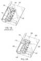
- FIGS. 1A-1Cseveral illustrative views of a conventional integrated-tube jack assembly are shown.
- FIG. 1Ashows an illustrative partial cut-way and isometric view of integrated-tube jack assembly 100 incorporated into housing 150.
- FIG. 1Bshows a side view and
- FIG. 1Cshows a top view of jack assembly 100 in housing 150, respectively.
- jack assembly 100includes a non-conductive component and several conductive components.
- the non-conductive componentincludes integrally formed body 106 and tube 110.
- the non-conductive componentcan be injected molded as a single integrated component.
- the conductive componentscan include electrical contacts 120 that are mounted to body 106.
- body 106 and tube 110requires a certain minimum thickness of the non-conductive component in order to form tube 110 of assembly 100.
- This minimum thickness for tube 110limits the ability to reduce the size of housing 150. For example, a reduction of z-height thickness of housing 150 is limited due to the minimum thickness needed to form 110.
- FIGS. 2A-2Cshows several views of a split jack assembly in accordance with an embodiment of the invention.
- FIG. 2Ashows an illustrative partial cut-way and isometric view of split jack assembly 200 incorporated into housing 250.
- FIG. 2Bshows a side view and
- FIG. 2Cshows a top view of split jack assembly 200 in housing 250, respectively.
- FIGS. 2A-2Ccollectively.
- split jack assembly 200can include tubeless pin block 210, tube 220, spring-loaded pins 230, and retention pin 232.
- Tubeless pin block 210 and tube 220are separate components and are not integrally formed, which is in direct contrast to conventional integrated-tube jack assembly 100 of FIG. 1 .
- Pins 230 and 232are conductive, but the other parts of pin block 210 are non-conductive.
- Tube 220is also non-conductive.
- Split jack assembly 200eliminates the integrated housing of assembly 100, and as a result, is able to reduce its footprint, compared to assembly 100.
- the reduced footprintcan be realized in that the separate pin block 210 and tube 220 construction allows for a thinner housing 250 in the z-height than housing 150.
- the two part construction of assembly 200does not require pin block to envelope tube 220, thus eliminating the minimum thickness requirement needed to form tube 110.
- Tubeless pin block 210includes curved abutting members 240 that are aligned along curved plane 242 and are interspersed with spring-loaded pins 230. A portion of each spring-loaded pin 230 can protrude beyond curved plane 242. Curved abutting members 240 are curved according to a predetermined radius. The predetermined radius can vary on a few factors such as the diameter of the plug to be inserted in the split jack assembly and/or whether a separate tube (e.g., tube 220) is used.
- a separate tubee.g., tube 220
- Block 210can include tube-stop abutting member 212, which can provide an anchor point for tube 220 if tube 220 is fixed to block 210.
- Retention pin 232can hold a plug (not shown) in place when it is inserted into the split jack assembly.
- tube 220can include one or more holes 222. Each hole 222 permit a spring-loaded pin 230 to pass through so that it can come into contact with a region of a plug (not shown).
- Tube 220has a predetermined diameter and wall thickness. The wall thickness can range between 50 and 200um, 75 and 125um, or be about 100um. Tube 220 may be an extruded material having non-conductive properties.
- tube 220is shown fixed to tubeless pin block 210.
- curved abutting members 240abut the outer surface of tube 220
- the edge of tube 220abuts tube-stop abutting member 212
- each one of spring-loaded pins 230protrude through one of holes 222.
- Tube 220may be fixed to block 210 using any suitable approach, such as, for example, adhesive (e.g., PSA), glue, or press fit.
- block 210 and tube 220can be subject to elevated temperatures that cause both to partially melt and bond together.
- Jack assembly 200can be positioned adjacent to a side of housing 250.
- block 210, tube 220, or bothmay be secured to housing 250 using glue, adhesive, or other suitable bonding agent or technique.
- gluefor example, can assist in enhanced strength of jack assembly 200 and can help eliminate ingress of water or debris into the housing 250.
- Housing 250can be any multi-walled structure that encloses various components of an electronic device. Some of the walls may be curved, as shown.
- side wall 253is curved and can be integrally formed with first surface member 251 and second surface member 252. The interior surface of sidewall 253 can be curved according to a predetermined radius.
- the interior surfacemay be dimensioned so that tube 220 fits snuggly against it when jack assembly 200 is installed in housing 250.
- the interior surface of housing 250may be dimensioned to accommodate a tubeless design (as shown in FIG. 5 ).
- the wall thickness of side wall 253 relative to wall thickness of tube 220may be substantially greater.
- the wall thickness of side wall 253may be 2-10 times greater than the wall thickness of tube 220.
- Enhanced wall thicknessmay be necessary because it bears some the lateral load exerted by the plug as it is inserted and retained within jack assembly 200.
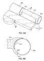
- FIG. 5shows a partial cut-away view of split jack assembly 500 incorporated inside housing 550 in accordance with an embodiment of the invention.
- Jack assembly 500can include tubeless pin block 510 and curved inner surface 553.
- Pin block 510can be the same or similar to pin block 210, as discussed above.
- the difference with jack assembly 500, compared to jack assembly 200,is that no separate tube is used as a receptacle for a plug. Rather, inner surface 553 and pin block 510 form the plug receptacle by being appropriately sized and placed together in appropriate proximity of each other.
- the radii of curvature of both inner surface 553 and curved abutting members 540can be substantially the same so that a receptacle of uniform diameter is provided for receiving a plug (not shown).
- an insulation layermay be applied to inner surface 553. If housing is constructed from metal, the insulation layer will prevent shorts when the plug is inserted. If an insulation layer is applied, then the dimensions of the inner surface are made so that the desired diameter is obtained for the plug receptacle.
- the insulation layermay be constructed from any suitable material and applied using using any suitable process.
- a materialmay be applied using spraying, painting, plasma vapor deposition (PVD), chemical vapor deposition (CVD), plasma enhanced chemical vapor deposition (PECVD), UV curing, high bake curing, thin tube extrusion (e.g., coupled to the housing using an adhesive, tape, bonding, or press fit), oxidation, electrolytic deposition, electrostatic deposition, plasma electrolytic oxide (PEO) process, a thermal spray coating, or any other suitable process.
- PVDplasma vapor deposition
- CVDchemical vapor deposition
- PECVDplasma enhanced chemical vapor deposition
- UV curinghigh bake curing
- thin tube extrusione.g., coupled to the housing using an adhesive, tape, bonding, or press fit
- oxidationelectrolytic deposition
- electrostatic depositionplasma electrolytic oxide (PEO) process
- thermal spray coatingor any other suitable process.
- Different materialsmay be used for each of the processes, including for example polyetheretherketone (PEEK), alumina, nitride (e.g., aluminum titanium nitride or silicon nitride), polyphenyl ether (PPE), diamond-like carbon coating (DLC), a plastic, polymer, composite material, or any other suitable material.
- PEEKpolyetheretherketone
- aluminae.g., aluminum titanium nitride or silicon nitride
- PPEpolyphenyl ether
- DLCdiamond-like carbon coating
- plasticpolymer, composite material, or any other suitable material.
- thin tube extrusione.g., using PEEK
- coatings applied by oxidation of the base metale.g., oxidation of the housing metal around the periphery of the port
- electrostatic deposition of ceramic coatingsmay provide adequate insulation on inner surface 553.
- the material and processmay be selected based on any suitable criteria.
- the materialmay be selected to be isolating (e.g., otherwise, it does not reduce undesired contacts between the connector and housing).
- Other criteriamay include, for example, selecting the material and process based on the appearance of the resulting layer or film (e.g., select a material that is substantially clear or transparent, or a material that is substantially the same color as the housing).
- the material and processmay be selected based on resistance to cracking, abrasive wear, or other failure (e.g., select a material and process that provide a layer operative to resist to a particular number of cycles of placing and removing a connector within the connector housing, or pulling a connector against the edges of the housing port).
- the material and processmay be selected for its applicability to different geometries (e.g., select a process and material that may be applied to ports in flat housings and curved housings).
- FIG. 6shows an illustrative process for assembling a jack assembly in accordance with an embodiment.
- a tubeless pin blockis secured within a housing, the tubeless pin block including a plurality of curved abutting members and a plurality of spring-loaded pins.
- the tubeless pin blockcan be block 210 of FIGS. 2 and 3 .
- a hollow tubecomprising a plurality of holes is fixed to the pin block such that the curved abutting members abut an outer surface of the hollow tube and the spring-loaded pins protrude through respective ones of the holes.
- the tubecan be tube 220 of FIGS. 4A-4B , for example.
- the tubecan be secured to the pin block by being inserted into the housing and rotated such that the spring-loaded pins protrude through their respective holes in the tube.
- the tubemay also be inserted into the housing until it abuts a tube-stop abutting member.
- FIGS. 7A-7B and 8A-8Bshow interlocking features that can be incorporated into the tube and pin block according to various embodiments. Interlocking features may be useful in securing the tube to the pin block and further enhancing ease of assembly.
- tube 700includes tab 710 and holes 722. Tab 722 can fit into a corresponding slot contained within the pin block (neither of which are shown). The tab/slot combination can assist in preventing tube 700 from rotating after it is installed. If desired, an adhesive can be used to glue tab 710 within the slot.
- FIG. 7Bshows tube 750 including tab 760, ribs 762, and holes 772.
- Tab 760can fit into a corresponding slot in a manner similar to tab 710 (of FIG. 7A ).
- Ribs 762can run along the length of tube 750, and in some embodiments, can also run along tab 760. Any number of ribs can be incorporated into tube 750. Thus, although three ribs are shown in the FIG. 7B , fewer or additional ribs can be incorporated.
- Ribs 762can fit into channels that run along the pin block (both of which are not shown). When ribs 762 are engaged with their respective channels in the pin block, the rib/channel combination is effective in preventing tube 750 from rotating, and it can facilitate ease of assembly.
- use of tab 760can be omitted and the tube can rely on use of ribs 762 to prevent rotation of tube 750.
- the interlocking featurescan be reversed.
- the slotcan exist on the tube and the tab member can exist in the pin block.
- the channelscan exist on the tube and the ribs can exist on the pin block.
- FIG. 8Ashows an illustrative perspective view of pin block 800 with tube 820 attached thereto in accordance with an embodiment.
- FIG. 8Bshows an illustrative cross-sectional view taken along line B-B of FIG. 8A .
- Pin block 800includes, among other features, curved member 810, tab member 812, and pins 814.
- Tube 820can includes holes (not shown) and slot 823.
- Tab member 812is part of curved member 810 and is constructed to fit into slot 823 when tube 820 is positioned next to pin block 800. The combination of tab member 812 and slot 823 can prevent tube 820 from rotating and sliding in the y-axis direction.
- curved member 810is can be attached to the outer surface of tube 820 with an adhesive.
- tab member 812is dimensioned to match the radius of tube 820.
- the inner diameter of tube 820remains substantially constant.
- the tubecan include a tab member operative to fit into a slot contained in the curved member.
Landscapes
- Connector Housings Or Holding Contact Members (AREA)
- Details Of Connecting Devices For Male And Female Coupling (AREA)
- Coupling Device And Connection With Printed Circuit (AREA)
Description
- This disclosure is directed to split jack assemblies and methods for making the same.
- Electronic devices may include jacks into which plugs may be inserted. The jack can include a number of contacts that come into contact with the plug when it is inserted into the jack. When inserted, signals can be transmitted between the plug and the jack. For example, an electronic device can generate audio signals that are provided from the jack to the plug, or the jack can receive microphone signals from the plug. As the size of electronic devices continue to shrink, and more features requiring more circuitry are incorporated therein, an ever increasing premium is made on space. Since the jack is often a necessary component included in electronic devices, there is a need for jacks having a reduced footprint.
US 2008/032562 A1 discloses an audio jack with pogo pins for conductive contacts, but suffers from a relatively larger size.US 7 988 498 B1 discloses a jack assembly having a hollow tube in two parts (reference signs 30 and 40), where one of the parts comprises the pin block (seeFig. 5 of this document). - This disclosure is directed to split jack assemblies and methods for making the same. Split jack assemblies according to embodiments of the invention are constructed with a tubeless pin block. Elimination (or split) of the tube, or more particularly, a tube that is an integrally formed part of the pin block form the pin block allows for the use of a tubeless pin block design that results in a jack assembly having smaller overall dimensions than a conventional jack assembly constructed to accommodate a plug of the same dimensions. The tubeless pin block can be used in conjunction with a tube sleeve or with a curved surface of a housing for an electronic device, or both to provide a plug receptacle region of the split jack assembly.
- The above and other objects and advantages of the invention will be apparent upon consideration of the following detailed description, taken in conjunction with the accompanying drawings, in which like reference characters refer to like parts throughout, and in which:
FIGS. 1A-1C show several illustrative views of a conventional integrated-tube jack assembly;FIGS. 2A-2C shows several views of a split jack assembly in accordance with an embodiment of the invention;FIGS. 3A-3C show several illustrative views of tubeless pin block in accordance with an embodiment;FIGS. 4A-4B show two illustrative views of a tube in accordance with one embodiment;FIG. 5 shows a partial cut-away view of a split jack assembly incorporated inside housing in accordance with an embodiment;FIG. 6 shows an illustrative flowchart for making a jack assembly in accordance with an embodiment; andFIGS. 7A-7B and8A-8B show illustrative interlocking features that can be incorporated into the tube and pin block according to various embodiments.- Split jack assemblies according to various embodiments are constructed with a tubeless pin block. Elimination (or split) of the tube, or more particularly, a tube that is an integrally formed part of the pin block form the pin block allows for the use of a tubeless pin block design that results in a jack assembly having smaller overall dimensions than a conventional jack assembly constructed to accommodate a plug of the same dimensions. The tubeless pin block can be used in conjunction with a tube sleeve or with a curved surface of a housing for an electronic device, or both to provide a plug receptacle region of the split jack assembly.
- Referring to
FIGS. 1A-1C , several illustrative views of a conventional integrated-tube jack assembly are shown.FIG. 1A shows an illustrative partial cut-way and isometric view of integrated-tube jack assembly 100 incorporated intohousing 150.FIG. 1B shows a side view andFIG. 1C shows a top view ofjack assembly 100 inhousing 150, respectively. Reference will be made toFIGS. 1A-1C collectively. As shown,jack assembly 100 includes a non-conductive component and several conductive components. The non-conductive component includes integrally formedbody 106 andtube 110. For example, the non-conductive component can be injected molded as a single integrated component. The conductive components can includeelectrical contacts 120 that are mounted tobody 106. The integral nature ofbody 106 andtube 110 requires a certain minimum thickness of the non-conductive component in order to formtube 110 ofassembly 100. This minimum thickness fortube 110 limits the ability to reduce the size ofhousing 150. For example, a reduction of z-height thickness ofhousing 150 is limited due to the minimum thickness needed to form 110. FIGS. 2A-2C shows several views of a split jack assembly in accordance with an embodiment of the invention.FIG. 2A shows an illustrative partial cut-way and isometric view ofsplit jack assembly 200 incorporated intohousing 250.FIG. 2B shows a side view andFIG. 2C shows a top view ofsplit jack assembly 200 inhousing 250, respectively. Reference will be made toFIGS. 2A-2C collectively. As shown,split jack assembly 200 can includetubeless pin block 210,tube 220, spring-loadedpins 230, andretention pin 232. Tubelesspin block 210 andtube 220 are separate components and are not integrally formed, which is in direct contrast to conventional integrated-tube jack assembly 100 ofFIG. 1 .Pins pin block 210 are non-conductive. Tube 220 is also non-conductive.Split jack assembly 200 eliminates the integrated housing ofassembly 100, and as a result, is able to reduce its footprint, compared toassembly 100. The reduced footprint can be realized in that theseparate pin block 210 andtube 220 construction allows for athinner housing 250 in the z-height thanhousing 150. The two part construction ofassembly 200 does not require pin block toenvelope tube 220, thus eliminating the minimum thickness requirement needed to formtube 110.- Referring briefly to
FIGS. 3A-3C , several illustrative views oftubeless pin block 210 are shown.Tubeless pin block 210 includes curved abuttingmembers 240 that are aligned alongcurved plane 242 and are interspersed with spring-loadedpins 230. A portion of each spring-loadedpin 230 can protrude beyondcurved plane 242. Curved abuttingmembers 240 are curved according to a predetermined radius. The predetermined radius can vary on a few factors such as the diameter of the plug to be inserted in the split jack assembly and/or whether a separate tube (e.g., tube 220) is used. - Block 210 can include tube-
stop abutting member 212, which can provide an anchor point fortube 220 iftube 220 is fixed to block 210.Retention pin 232 can hold a plug (not shown) in place when it is inserted into the split jack assembly. - Referring now to
FIGS 4A-4B , two illustrative views oftube 220. As shown,tube 220 can include one ormore holes 222. Eachhole 222 permit a spring-loadedpin 230 to pass through so that it can come into contact with a region of a plug (not shown).Tube 220 has a predetermined diameter and wall thickness. The wall thickness can range between 50 and 200um, 75 and 125um, or be about 100um.Tube 220 may be an extruded material having non-conductive properties. - Referring back to
FIGS. 2A-2C ,tube 220 is shown fixed totubeless pin block 210. Whentube 220 is fixed to block 210, curved abuttingmembers 240 abut the outer surface oftube 220, the edge oftube 220 abuts tube-stop abutting member 212, and each one of spring-loadedpins 230 protrude through one ofholes 222.Tube 220 may be fixed to block 210 using any suitable approach, such as, for example, adhesive (e.g., PSA), glue, or press fit. In another approach, block 210 andtube 220 can be subject to elevated temperatures that cause both to partially melt and bond together. Jack assembly 200 can be positioned adjacent to a side ofhousing 250. In some embodiments, block 210,tube 220, or both may be secured tohousing 250 using glue, adhesive, or other suitable bonding agent or technique. Use of glue, for example, can assist in enhanced strength ofjack assembly 200 and can help eliminate ingress of water or debris into thehousing 250. Housing 250 can be any multi-walled structure that encloses various components of an electronic device. Some of the walls may be curved, as shown. In particular,side wall 253 is curved and can be integrally formed withfirst surface member 251 andsecond surface member 252. The interior surface ofsidewall 253 can be curved according to a predetermined radius. Moreover, in some embodiments, the interior surface may be dimensioned so thattube 220 fits snuggly against it whenjack assembly 200 is installed inhousing 250. In other embodiments, the interior surface ofhousing 250 may be dimensioned to accommodate a tubeless design (as shown inFIG. 5 ).- The wall thickness of
side wall 253 relative to wall thickness oftube 220 may be substantially greater. For example, the wall thickness ofside wall 253 may be 2-10 times greater than the wall thickness oftube 220. Enhanced wall thickness may be necessary because it bears some the lateral load exerted by the plug as it is inserted and retained withinjack assembly 200. FIG. 5 shows a partial cut-away view of split jack assembly 500 incorporated insidehousing 550 in accordance with an embodiment of the invention. Jack assembly 500 can includetubeless pin block 510 and curvedinner surface 553.Pin block 510 can be the same or similar to pin block 210, as discussed above. The difference with jack assembly 500, compared tojack assembly 200, is that no separate tube is used as a receptacle for a plug. Rather,inner surface 553 and pin block 510 form the plug receptacle by being appropriately sized and placed together in appropriate proximity of each other. Thus, the radii of curvature of bothinner surface 553 and curved abuttingmembers 540 can be substantially the same so that a receptacle of uniform diameter is provided for receiving a plug (not shown).- In some embodiments, depending on the material composition of
housing 550, an insulation layer may be applied toinner surface 553. If housing is constructed from metal, the insulation layer will prevent shorts when the plug is inserted. If an insulation layer is applied, then the dimensions of the inner surface are made so that the desired diameter is obtained for the plug receptacle. - The insulation layer may be constructed from any suitable material and applied using using any suitable process. For example, a material may be applied using spraying, painting, plasma vapor deposition (PVD), chemical vapor deposition (CVD), plasma enhanced chemical vapor deposition (PECVD), UV curing, high bake curing, thin tube extrusion (e.g., coupled to the housing using an adhesive, tape, bonding, or press fit), oxidation, electrolytic deposition, electrostatic deposition, plasma electrolytic oxide (PEO) process, a thermal spray coating, or any other suitable process. Different materials may be used for each of the processes, including for example polyetheretherketone (PEEK), alumina, nitride (e.g., aluminum titanium nitride or silicon nitride), polyphenyl ether (PPE), diamond-like carbon coating (DLC), a plastic, polymer, composite material, or any other suitable material. In some embodiments, thin tube extrusion (e.g., using PEEK), coatings applied by oxidation of the base metal (e.g., oxidation of the housing metal around the periphery of the port), or electrostatic deposition of ceramic coatings may provide adequate insulation on
inner surface 553. - The material and process may be selected based on any suitable criteria. In particular, the material may be selected to be isolating (e.g., otherwise, it does not reduce undesired contacts between the connector and housing). Other criteria may include, for example, selecting the material and process based on the appearance of the resulting layer or film (e.g., select a material that is substantially clear or transparent, or a material that is substantially the same color as the housing). As another example, the material and process may be selected based on resistance to cracking, abrasive wear, or other failure (e.g., select a material and process that provide a layer operative to resist to a particular number of cycles of placing and removing a connector within the connector housing, or pulling a connector against the edges of the housing port). As still another example, the material and process may be selected for its applicability to different geometries (e.g., select a process and material that may be applied to ports in flat housings and curved housings).
FIG. 6 shows an illustrative process for assembling a jack assembly in accordance with an embodiment. Beginning atstep 610, a tubeless pin block is secured within a housing, the tubeless pin block including a plurality of curved abutting members and a plurality of spring-loaded pins. For example, the tubeless pin block can be block 210 ofFIGS. 2 and3 . Atstep 620, a hollow tube comprising a plurality of holes is fixed to the pin block such that the curved abutting members abut an outer surface of the hollow tube and the spring-loaded pins protrude through respective ones of the holes. The tube can betube 220 ofFIGS. 4A-4B , for example.- The tube can be secured to the pin block by being inserted into the housing and rotated such that the spring-loaded pins protrude through their respective holes in the tube. The tube may also be inserted into the housing until it abuts a tube-stop abutting member.
FIGS. 7A-7B and8A-8B show interlocking features that can be incorporated into the tube and pin block according to various embodiments. Interlocking features may be useful in securing the tube to the pin block and further enhancing ease of assembly. Referring now toFIG. 7A ,tube 700 includestab 710 and holes 722.Tab 722 can fit into a corresponding slot contained within the pin block (neither of which are shown). The tab/slot combination can assist in preventingtube 700 from rotating after it is installed. If desired, an adhesive can be used toglue tab 710 within the slot.FIG. 7B showstube 750 including tab 760,ribs 762, and holes 772. Tab 760 can fit into a corresponding slot in a manner similar to tab 710 (ofFIG. 7A ).Ribs 762 can run along the length oftube 750, and in some embodiments, can also run along tab 760. Any number of ribs can be incorporated intotube 750. Thus, although three ribs are shown in theFIG. 7B , fewer or additional ribs can be incorporated.Ribs 762 can fit into channels that run along the pin block (both of which are not shown). Whenribs 762 are engaged with their respective channels in the pin block, the rib/channel combination is effective in preventingtube 750 from rotating, and it can facilitate ease of assembly. In some embodiments, use of tab 760 can be omitted and the tube can rely on use ofribs 762 to prevent rotation oftube 750.- It is understood that the interlocking features can be reversed. For example, the slot can exist on the tube and the tab member can exist in the pin block. As another example, the channels can exist on the tube and the ribs can exist on the pin block.
FIG. 8A shows an illustrative perspective view ofpin block 800 withtube 820 attached thereto in accordance with an embodiment.FIG. 8B shows an illustrative cross-sectional view taken along line B-B ofFIG. 8A . Reference will be made toFIGS. 8A-8B collectively.Pin block 800 includes, among other features,curved member 810,tab member 812, and pins 814.Tube 820 can includes holes (not shown) andslot 823.Tab member 812 is part ofcurved member 810 and is constructed to fit intoslot 823 whentube 820 is positioned next to pinblock 800. The combination oftab member 812 and slot 823 can preventtube 820 from rotating and sliding in the y-axis direction. In some embodiments,curved member 810 is can be attached to the outer surface oftube 820 with an adhesive.- Referring specifically to
FIG. 8B , the surface oftab member 812 is dimensioned to match the radius oftube 820. Thus, even thoughtab member 812 is inserted into a slot (not shown) contained withintube 820, the inner diameter oftube 820 remains substantially constant. - It is understood that the tab member and slot can be reversed. For example, the tube can include a tab member operative to fit into a slot contained in the curved member.
- The above described embodiments of the invention are presented for purposes of illustration and not of limitation, and the present invention is limited only by the claims which follow.
Claims (13)
- A jack assembly (200) for use with a plug, the jack assembly (200) comprising:a tubeless pin block (210) comprising:a plurality of curved abutting members (240); anda plurality of spring-loaded pins (230), each spring-loaded pin (230) positioned within one of the curved abutting members (240) and operative to protrude beyond a curved plane formed by the curved abutting members; anda hollow tube (220) including a plurality of holes (222) and fixed to the tubeless pin block (210) such that the curved abutting members abut an outer surface of the hollow-tube (220) and the spring-loaded pins (230) protrude through respective ones of the holes (222).
- The jack assembly of claim 1, wherein the tube (220) is constructed from a non-conductive material.
- The jack assembly of claim 1 or claim 2, wherein the curved abutting members are constructed from a non-conductive material.
- The jack assembly of any preceding claim, wherein the tubeless pin block (210) comprises a retention pin (232).
- The jack assembly of any preceding claim, wherein the tubeless pin block (210) comprises a tube-stop abutting member (212), and wherein an end of the hollow tube (220) abuts the tube-stop abutting member (212).
- The jack assembly of any preceding claim, wherein the tubeless pin block (210) and hollow tube (220) are separate components that are not integrally formed together.
- The jack assembly of any preceding claim, further comprising:a housing (250) having a curved surface (253), wherein the tube (220) is secured to the curved surface (253) of the housing (250).
- The jack assembly of any preceding claim, wherein the tubeless pin block (210) comprises a slot, and wherein the hollow tube (220) comprises a tab (722) operative to fit into the slot.
- The jack assembly of any preceding claim, wherein the tubeless pin block (210) comprises at least one channel, and wherein the hollow tube (220) comprises at least one rib (762) operated to fit within its respective at least one channel.
- A method for manufacturing a jack assembly, the method comprising:securing a tubeless pin block within a housing, the tubeless pin block comprising a plurality of curved abutting members and a plurality of spring-loaded pins; andfixing a hollow tube comprising a plurality of holes to the pin block such that the curved abutting members abut an outer surface of the hollow tube and the spring-loaded pins protrude through respective ones of the holes.
- The method of claim 10, wherein the housing comprises a curved surface, and a portion of the outer surface of the hollow tube is secured to the curved surface.
- The method of claim 10 or claim 11, wherein fixing a hollow tube to the pin comprises:inserting the hollow tube into the housing; androtating the hollow tube until the spring-loaded pins protrude through their respective holes.
- The method of any of claims 10 to 12, further comprising:inserting the hollow tube member into the housing until it abuts a tube-stop abutting member of the tubeless pin block.
Applications Claiming Priority (3)
| Application Number | Priority Date | Filing Date | Title |
|---|---|---|---|
| US201161553109P | 2011-10-28 | 2011-10-28 | |
| US201161555131P | 2011-11-03 | 2011-11-03 | |
| PCT/US2012/059765WO2013062780A1 (en) | 2011-10-28 | 2012-10-11 | Split jack assemblies and methods for making the same |
Publications (2)
| Publication Number | Publication Date |
|---|---|
| EP2754207A1 EP2754207A1 (en) | 2014-07-16 |
| EP2754207B1true EP2754207B1 (en) | 2016-03-02 |
Family
ID=47221532
Family Applications (1)
| Application Number | Title | Priority Date | Filing Date |
|---|---|---|---|
| EP12790706.1ANot-in-forceEP2754207B1 (en) | 2011-10-28 | 2012-10-11 | Split jack assemblies and methods for making the same |
Country Status (8)
| Country | Link |
|---|---|
| US (2) | US8668528B2 (en) |
| EP (1) | EP2754207B1 (en) |
| JP (1) | JP5750197B2 (en) |
| KR (1) | KR101602082B1 (en) |
| CN (1) | CN103907244B (en) |
| AU (1) | AU2012329205B2 (en) |
| TW (2) | TW201338317A (en) |
| WO (1) | WO2013062780A1 (en) |
Families Citing this family (7)
| Publication number | Priority date | Publication date | Assignee | Title |
|---|---|---|---|---|
| US8668528B2 (en)* | 2011-10-28 | 2014-03-11 | Apple Inc. | Split jack assemblies and methods for making the same |
| US9478886B1 (en)* | 2014-06-10 | 2016-10-25 | Google Inc. | Jack with cylindrical housing |
| US9130302B1 (en)* | 2014-07-10 | 2015-09-08 | Cheng Uei Precision Industry Co., Ltd. | Audio jack connector |
| USD789924S1 (en) | 2015-01-16 | 2017-06-20 | Apple Inc. | Electronic device |
| JP1573612S (en) | 2016-02-27 | 2017-04-10 | ||
| USD947834S1 (en)* | 2016-03-21 | 2022-04-05 | Apple Inc. | Electronic device |
| US10828496B2 (en)* | 2018-07-12 | 2020-11-10 | Cardiac Pacemakers, Inc. | Core-clip PG-lead spring electrical contact |
Family Cites Families (37)
| Publication number | Priority date | Publication date | Assignee | Title |
|---|---|---|---|---|
| US419365A (en)* | 1890-01-14 | Electric connector | ||
| US1876695A (en)* | 1928-02-06 | 1932-09-13 | American Electrical Heater Co | Electric plug |
| US3794961A (en)* | 1971-05-03 | 1974-02-26 | Switchcraft | Electrical twin plug |
| US4165147A (en)* | 1978-06-05 | 1979-08-21 | Magnetic Controls Company | Printed circuit board jack |
| US4364625A (en)* | 1980-06-12 | 1982-12-21 | Bell Telephone Laboratories, Incorporated | Electrical jack assembly |
| US4367907A (en)* | 1980-08-04 | 1983-01-11 | Magnetic Controls Company | Circuit monitoring jack |
| US5181859A (en) | 1991-04-29 | 1993-01-26 | Trw Inc. | Electrical connector circuit wafer |
| US5511995A (en)* | 1994-10-31 | 1996-04-30 | Cheng; Yu F. | Direct current connector |
| US5809136A (en)* | 1996-01-16 | 1998-09-15 | Turner; Robert A. | Circumferential-contact phone jack socket |
| JP2000340311A (en)* | 1999-05-31 | 2000-12-08 | Mitsumi Electric Co Ltd | Electric connector |
| CN2604801Y (en)* | 2003-03-21 | 2004-02-25 | 莫列斯公司 | Combined connector |
| CN2609231Y (en) | 2003-03-21 | 2004-03-31 | 莫列斯公司 | Audio frequency socket connector |
| TWM259352U (en) | 2004-07-12 | 2005-03-11 | Excel Cell Elect Co Ltd | Ear phone plug |
| CN2850025Y (en)* | 2005-11-14 | 2006-12-20 | 富士康(昆山)电脑接插件有限公司 | Speech socket connector |
| WO2007084125A1 (en)* | 2006-01-17 | 2007-07-26 | Jeffery H Purchon Jeffery | Self-muting audio connector |
| DE102006018716A1 (en)* | 2006-04-20 | 2007-10-25 | Ebm-Papst Mulfingen Gmbh & Co. Kg | Arrangement for contacting power semiconductors on a cooling surface |
| US7371125B2 (en)* | 2006-07-24 | 2008-05-13 | Hon Hai Precision Ind. Co., Ltd. | Miniature audio jack connector |
| JP5094343B2 (en)* | 2007-11-20 | 2012-12-12 | 第一電子工業株式会社 | Connector and method for inspecting connection portion of connector |
| CN201207526Y (en) | 2008-04-30 | 2009-03-11 | 富士康(昆山)电脑接插件有限公司 | Electric connector |
| JP2010033193A (en) | 2008-07-25 | 2010-02-12 | Fujitsu Ltd | Authentication system and authentication server device |
| US7815471B2 (en)* | 2008-08-01 | 2010-10-19 | Hon Hai Precision Ind. Co., Ltd. | Rotatable electrical interconnection device |
| US8360801B2 (en)* | 2009-01-21 | 2013-01-29 | Apple Inc. | Contactless plug detect mechanism |
| US7942705B2 (en)* | 2009-03-20 | 2011-05-17 | Apple Inc. | Audio jack with pogo pins for conductive contacts |
| CN101877948A (en)* | 2009-04-30 | 2010-11-03 | 深圳富泰宏精密工业有限公司 | Electronic device |
| TWM371338U (en)* | 2009-06-19 | 2009-12-21 | Cheng Uei Prec Ind Co Ltd | Audio jack connector |
| CN201449747U (en)* | 2009-06-30 | 2010-05-05 | 冼小勇 | Music player |
| US8215989B2 (en) | 2009-10-05 | 2012-07-10 | Research In Motion Limited | Audio jack with EMI shielding |
| US7950966B1 (en)* | 2009-12-17 | 2011-05-31 | Cheng Uei Precision Industry Co., Ltd. | Audio jack connector |
| US8123569B2 (en) | 2010-02-08 | 2012-02-28 | Hon Hai Precision Ind. Co., Ltd. | Waterproof audio jack connector |
| SG185731A1 (en)* | 2010-05-28 | 2013-01-30 | Apple Inc | Dual orientation connector with external contacts |
| CN201774062U (en)* | 2010-06-04 | 2011-03-23 | 富士康(昆山)电脑接插件有限公司 | audio connector |
| DE102010051899B4 (en)* | 2010-11-22 | 2015-03-26 | Wago Verwaltungsgesellschaft Mbh | Electrical terminal component |
| KR101113592B1 (en) | 2010-12-06 | 2012-02-22 | 암페놀커머셜인터커넥트코리아(주) | Earphone jack |
| TWM414008U (en)* | 2011-05-13 | 2011-10-11 | Apex Prec Technology Corp | Terminal fixing structure for signal connector |
| US8834208B2 (en) | 2011-10-03 | 2014-09-16 | Blackberry Limited | Low profile electrical connector |
| US8668528B2 (en)* | 2011-10-28 | 2014-03-11 | Apple Inc. | Split jack assemblies and methods for making the same |
| US9332339B2 (en)* | 2012-10-05 | 2016-05-03 | Qualcomm Incorporated | Multi-pin audio plug with retractable nub |
- 2012
- 2012-09-28USUS13/631,553patent/US8668528B2/ennot_activeExpired - Fee Related
- 2012-10-11AUAU2012329205Apatent/AU2012329205B2/ennot_activeCeased
- 2012-10-11EPEP12790706.1Apatent/EP2754207B1/ennot_activeNot-in-force
- 2012-10-11KRKR1020147014424Apatent/KR101602082B1/ennot_activeExpired - Fee Related
- 2012-10-11WOPCT/US2012/059765patent/WO2013062780A1/enactiveApplication Filing
- 2012-10-11JPJP2014538826Apatent/JP5750197B2/ennot_activeExpired - Fee Related
- 2012-10-11CNCN201280052462.7Apatent/CN103907244B/ennot_activeExpired - Fee Related
- 2012-10-26TWTW102116789Apatent/TW201338317A/enunknown
- 2012-10-26TWTW101139843Apatent/TWI489712B/ennot_activeIP Right Cessation
- 2014
- 2014-02-20USUS14/185,133patent/US9331438B2/enactiveActive
Also Published As
| Publication number | Publication date |
|---|---|
| EP2754207A1 (en) | 2014-07-16 |
| US20140170905A1 (en) | 2014-06-19 |
| TWI489712B (en) | 2015-06-21 |
| CN103907244A (en) | 2014-07-02 |
| WO2013062780A1 (en) | 2013-05-02 |
| JP5750197B2 (en) | 2015-07-15 |
| TW201338317A (en) | 2013-09-16 |
| AU2012329205A1 (en) | 2014-04-17 |
| KR101602082B1 (en) | 2016-03-17 |
| CN103907244B (en) | 2017-04-12 |
| US8668528B2 (en) | 2014-03-11 |
| JP2014534583A (en) | 2014-12-18 |
| AU2012329205B2 (en) | 2015-12-03 |
| US9331438B2 (en) | 2016-05-03 |
| KR20140091027A (en) | 2014-07-18 |
| US20130109248A1 (en) | 2013-05-02 |
| TW201330429A (en) | 2013-07-16 |
Similar Documents
| Publication | Publication Date | Title |
|---|---|---|
| EP2754207B1 (en) | Split jack assemblies and methods for making the same | |
| JP5131937B2 (en) | Electrical connector for panel mounting | |
| EP1736569B1 (en) | Electroplating jig | |
| EP2462658B1 (en) | Multiple layer conductor pin for electrical connector and method of manufacture | |
| US8313336B2 (en) | Assembly comprising a male and a female plug member, a male plug member and a female plug member | |
| CN103597366B (en) | Insulated metal socket | |
| EP2438653A1 (en) | Coaxial connector interconnection cap | |
| EP2093576A1 (en) | Conductive contact holder, conductive contact unit and method for manufacturing conductive contact holder | |
| US20080139047A1 (en) | Cable Connector Expanding Contact | |
| WO2007040958A3 (en) | Electrostatic chuck assembly with dielectric material and/or cavity having varying thickness, profile and/or shape, method of use and apparatus incorporating same | |
| WO2005033663A3 (en) | Methods of making substrates for mass spectrometry analysis and related devices | |
| US8328584B2 (en) | Systems and methods for providing a trimless electronic device port | |
| EP4230562A1 (en) | Chuck assembly for holding reel | |
| CN107851939B (en) | Dielectric Isolators for Coaxial Cables and Connectors | |
| TWI578650B (en) | Insulated metal socket | |
| US20070119044A1 (en) | Clamping device for flexible substrate and method for fabricating the same | |
| US11075471B2 (en) | Coaxial cable and connector with dielectric spacer that inhibits unwanted solder flow | |
| WO2018146369A1 (en) | A circuit board system and method for manufacturing the same |
Legal Events
| Date | Code | Title | Description |
|---|---|---|---|
| PUAI | Public reference made under article 153(3) epc to a published international application that has entered the european phase | Free format text:ORIGINAL CODE: 0009012 | |
| 17P | Request for examination filed | Effective date:20140411 | |
| AK | Designated contracting states | Kind code of ref document:A1 Designated state(s):AL AT BE BG CH CY CZ DE DK EE ES FI FR GB GR HR HU IE IS IT LI LT LU LV MC MK MT NL NO PL PT RO RS SE SI SK SM TR | |
| DAX | Request for extension of the european patent (deleted) | ||
| 17Q | First examination report despatched | Effective date:20150216 | |
| GRAP | Despatch of communication of intention to grant a patent | Free format text:ORIGINAL CODE: EPIDOSNIGR1 | |
| INTG | Intention to grant announced | Effective date:20150519 | |
| GRAJ | Information related to disapproval of communication of intention to grant by the applicant or resumption of examination proceedings by the epo deleted | Free format text:ORIGINAL CODE: EPIDOSDIGR1 | |
| GRAP | Despatch of communication of intention to grant a patent | Free format text:ORIGINAL CODE: EPIDOSNIGR1 | |
| INTG | Intention to grant announced | Effective date:20150806 | |
| GRAS | Grant fee paid | Free format text:ORIGINAL CODE: EPIDOSNIGR3 | |
| GRAA | (expected) grant | Free format text:ORIGINAL CODE: 0009210 | |
| AK | Designated contracting states | Kind code of ref document:B1 Designated state(s):AL AT BE BG CH CY CZ DE DK EE ES FI FR GB GR HR HU IE IS IT LI LT LU LV MC MK MT NL NO PL PT RO RS SE SI SK SM TR | |
| REG | Reference to a national code | Ref country code:GB Ref legal event code:FG4D | |
| REG | Reference to a national code | Ref country code:AT Ref legal event code:REF Ref document number:778587 Country of ref document:AT Kind code of ref document:T Effective date:20160315 Ref country code:CH Ref legal event code:EP | |
| REG | Reference to a national code | Ref country code:IE Ref legal event code:FG4D | |
| REG | Reference to a national code | Ref country code:DE Ref legal event code:R096 Ref document number:602012015274 Country of ref document:DE | |
| REG | Reference to a national code | Ref country code:NL Ref legal event code:MP Effective date:20160302 | |
| REG | Reference to a national code | Ref country code:LT Ref legal event code:MG4D | |
| REG | Reference to a national code | Ref country code:AT Ref legal event code:MK05 Ref document number:778587 Country of ref document:AT Kind code of ref document:T Effective date:20160302 | |
| PG25 | Lapsed in a contracting state [announced via postgrant information from national office to epo] | Ref country code:FI Free format text:LAPSE BECAUSE OF FAILURE TO SUBMIT A TRANSLATION OF THE DESCRIPTION OR TO PAY THE FEE WITHIN THE PRESCRIBED TIME-LIMIT Effective date:20160302 Ref country code:NO Free format text:LAPSE BECAUSE OF FAILURE TO SUBMIT A TRANSLATION OF THE DESCRIPTION OR TO PAY THE FEE WITHIN THE PRESCRIBED TIME-LIMIT Effective date:20160602 Ref country code:GR Free format text:LAPSE BECAUSE OF FAILURE TO SUBMIT A TRANSLATION OF THE DESCRIPTION OR TO PAY THE FEE WITHIN THE PRESCRIBED TIME-LIMIT Effective date:20160603 Ref country code:ES Free format text:LAPSE BECAUSE OF FAILURE TO SUBMIT A TRANSLATION OF THE DESCRIPTION OR TO PAY THE FEE WITHIN THE PRESCRIBED TIME-LIMIT Effective date:20160302 Ref country code:HR Free format text:LAPSE BECAUSE OF FAILURE TO SUBMIT A TRANSLATION OF THE DESCRIPTION OR TO PAY THE FEE WITHIN THE PRESCRIBED TIME-LIMIT Effective date:20160302 | |
| PG25 | Lapsed in a contracting state [announced via postgrant information from national office to epo] | Ref country code:RS Free format text:LAPSE BECAUSE OF FAILURE TO SUBMIT A TRANSLATION OF THE DESCRIPTION OR TO PAY THE FEE WITHIN THE PRESCRIBED TIME-LIMIT Effective date:20160302 Ref country code:SE Free format text:LAPSE BECAUSE OF FAILURE TO SUBMIT A TRANSLATION OF THE DESCRIPTION OR TO PAY THE FEE WITHIN THE PRESCRIBED TIME-LIMIT Effective date:20160302 Ref country code:LT Free format text:LAPSE BECAUSE OF FAILURE TO SUBMIT A TRANSLATION OF THE DESCRIPTION OR TO PAY THE FEE WITHIN THE PRESCRIBED TIME-LIMIT Effective date:20160302 Ref country code:NL Free format text:LAPSE BECAUSE OF FAILURE TO SUBMIT A TRANSLATION OF THE DESCRIPTION OR TO PAY THE FEE WITHIN THE PRESCRIBED TIME-LIMIT Effective date:20160302 Ref country code:PL Free format text:LAPSE BECAUSE OF FAILURE TO SUBMIT A TRANSLATION OF THE DESCRIPTION OR TO PAY THE FEE WITHIN THE PRESCRIBED TIME-LIMIT Effective date:20160302 Ref country code:AT Free format text:LAPSE BECAUSE OF FAILURE TO SUBMIT A TRANSLATION OF THE DESCRIPTION OR TO PAY THE FEE WITHIN THE PRESCRIBED TIME-LIMIT Effective date:20160302 Ref country code:LV Free format text:LAPSE BECAUSE OF FAILURE TO SUBMIT A TRANSLATION OF THE DESCRIPTION OR TO PAY THE FEE WITHIN THE PRESCRIBED TIME-LIMIT Effective date:20160302 | |
| PG25 | Lapsed in a contracting state [announced via postgrant information from national office to epo] | Ref country code:EE Free format text:LAPSE BECAUSE OF FAILURE TO SUBMIT A TRANSLATION OF THE DESCRIPTION OR TO PAY THE FEE WITHIN THE PRESCRIBED TIME-LIMIT Effective date:20160302 Ref country code:IS Free format text:LAPSE BECAUSE OF FAILURE TO SUBMIT A TRANSLATION OF THE DESCRIPTION OR TO PAY THE FEE WITHIN THE PRESCRIBED TIME-LIMIT Effective date:20160702 | |
| PG25 | Lapsed in a contracting state [announced via postgrant information from national office to epo] | Ref country code:SM Free format text:LAPSE BECAUSE OF FAILURE TO SUBMIT A TRANSLATION OF THE DESCRIPTION OR TO PAY THE FEE WITHIN THE PRESCRIBED TIME-LIMIT Effective date:20160302 Ref country code:RO Free format text:LAPSE BECAUSE OF FAILURE TO SUBMIT A TRANSLATION OF THE DESCRIPTION OR TO PAY THE FEE WITHIN THE PRESCRIBED TIME-LIMIT Effective date:20160302 Ref country code:SK Free format text:LAPSE BECAUSE OF FAILURE TO SUBMIT A TRANSLATION OF THE DESCRIPTION OR TO PAY THE FEE WITHIN THE PRESCRIBED TIME-LIMIT Effective date:20160302 Ref country code:PT Free format text:LAPSE BECAUSE OF FAILURE TO SUBMIT A TRANSLATION OF THE DESCRIPTION OR TO PAY THE FEE WITHIN THE PRESCRIBED TIME-LIMIT Effective date:20160704 Ref country code:CZ Free format text:LAPSE BECAUSE OF FAILURE TO SUBMIT A TRANSLATION OF THE DESCRIPTION OR TO PAY THE FEE WITHIN THE PRESCRIBED TIME-LIMIT Effective date:20160302 | |
| REG | Reference to a national code | Ref country code:DE Ref legal event code:R097 Ref document number:602012015274 Country of ref document:DE | |
| PG25 | Lapsed in a contracting state [announced via postgrant information from national office to epo] | Ref country code:BE Free format text:LAPSE BECAUSE OF FAILURE TO SUBMIT A TRANSLATION OF THE DESCRIPTION OR TO PAY THE FEE WITHIN THE PRESCRIBED TIME-LIMIT Effective date:20160302 Ref country code:IT Free format text:LAPSE BECAUSE OF FAILURE TO SUBMIT A TRANSLATION OF THE DESCRIPTION OR TO PAY THE FEE WITHIN THE PRESCRIBED TIME-LIMIT Effective date:20160302 | |
| PLBE | No opposition filed within time limit | Free format text:ORIGINAL CODE: 0009261 | |
| STAA | Information on the status of an ep patent application or granted ep patent | Free format text:STATUS: NO OPPOSITION FILED WITHIN TIME LIMIT | |
| PG25 | Lapsed in a contracting state [announced via postgrant information from national office to epo] | Ref country code:DK Free format text:LAPSE BECAUSE OF FAILURE TO SUBMIT A TRANSLATION OF THE DESCRIPTION OR TO PAY THE FEE WITHIN THE PRESCRIBED TIME-LIMIT Effective date:20160302 | |
| 26N | No opposition filed | Effective date:20161205 | |
| PG25 | Lapsed in a contracting state [announced via postgrant information from national office to epo] | Ref country code:BG Free format text:LAPSE BECAUSE OF FAILURE TO SUBMIT A TRANSLATION OF THE DESCRIPTION OR TO PAY THE FEE WITHIN THE PRESCRIBED TIME-LIMIT Effective date:20160602 Ref country code:SI Free format text:LAPSE BECAUSE OF FAILURE TO SUBMIT A TRANSLATION OF THE DESCRIPTION OR TO PAY THE FEE WITHIN THE PRESCRIBED TIME-LIMIT Effective date:20160302 | |
| REG | Reference to a national code | Ref country code:CH Ref legal event code:PL | |
| REG | Reference to a national code | Ref country code:IE Ref legal event code:MM4A | |
| REG | Reference to a national code | Ref country code:FR Ref legal event code:ST Effective date:20170630 | |
| PG25 | Lapsed in a contracting state [announced via postgrant information from national office to epo] | Ref country code:FR Free format text:LAPSE BECAUSE OF NON-PAYMENT OF DUE FEES Effective date:20161102 Ref country code:CH Free format text:LAPSE BECAUSE OF NON-PAYMENT OF DUE FEES Effective date:20161031 Ref country code:LI Free format text:LAPSE BECAUSE OF NON-PAYMENT OF DUE FEES Effective date:20161031 | |
| PG25 | Lapsed in a contracting state [announced via postgrant information from national office to epo] | Ref country code:LU Free format text:LAPSE BECAUSE OF NON-PAYMENT OF DUE FEES Effective date:20161011 | |
| PG25 | Lapsed in a contracting state [announced via postgrant information from national office to epo] | Ref country code:IE Free format text:LAPSE BECAUSE OF NON-PAYMENT OF DUE FEES Effective date:20161011 | |
| PGFP | Annual fee paid to national office [announced via postgrant information from national office to epo] | Ref country code:GB Payment date:20171011 Year of fee payment:6 | |
| PG25 | Lapsed in a contracting state [announced via postgrant information from national office to epo] | Ref country code:HU Free format text:LAPSE BECAUSE OF FAILURE TO SUBMIT A TRANSLATION OF THE DESCRIPTION OR TO PAY THE FEE WITHIN THE PRESCRIBED TIME-LIMIT; INVALID AB INITIO Effective date:20121011 | |
| PG25 | Lapsed in a contracting state [announced via postgrant information from national office to epo] | Ref country code:CY Free format text:LAPSE BECAUSE OF FAILURE TO SUBMIT A TRANSLATION OF THE DESCRIPTION OR TO PAY THE FEE WITHIN THE PRESCRIBED TIME-LIMIT Effective date:20160302 Ref country code:MK Free format text:LAPSE BECAUSE OF FAILURE TO SUBMIT A TRANSLATION OF THE DESCRIPTION OR TO PAY THE FEE WITHIN THE PRESCRIBED TIME-LIMIT Effective date:20160302 Ref country code:MC Free format text:LAPSE BECAUSE OF FAILURE TO SUBMIT A TRANSLATION OF THE DESCRIPTION OR TO PAY THE FEE WITHIN THE PRESCRIBED TIME-LIMIT Effective date:20160302 Ref country code:MT Free format text:LAPSE BECAUSE OF NON-PAYMENT OF DUE FEES Effective date:20161031 | |
| PG25 | Lapsed in a contracting state [announced via postgrant information from national office to epo] | Ref country code:AL Free format text:LAPSE BECAUSE OF FAILURE TO SUBMIT A TRANSLATION OF THE DESCRIPTION OR TO PAY THE FEE WITHIN THE PRESCRIBED TIME-LIMIT Effective date:20160302 Ref country code:TR Free format text:LAPSE BECAUSE OF FAILURE TO SUBMIT A TRANSLATION OF THE DESCRIPTION OR TO PAY THE FEE WITHIN THE PRESCRIBED TIME-LIMIT Effective date:20160302 | |
| PGFP | Annual fee paid to national office [announced via postgrant information from national office to epo] | Ref country code:DE Payment date:20180925 Year of fee payment:7 | |
| GBPC | Gb: european patent ceased through non-payment of renewal fee | Effective date:20181011 | |
| PG25 | Lapsed in a contracting state [announced via postgrant information from national office to epo] | Ref country code:GB Free format text:LAPSE BECAUSE OF NON-PAYMENT OF DUE FEES Effective date:20181011 | |
| REG | Reference to a national code | Ref country code:DE Ref legal event code:R119 Ref document number:602012015274 Country of ref document:DE | |
| PG25 | Lapsed in a contracting state [announced via postgrant information from national office to epo] | Ref country code:DE Free format text:LAPSE BECAUSE OF NON-PAYMENT OF DUE FEES Effective date:20200501 |