EP2752081B2 - Thermal array system - Google Patents
Thermal array systemDownload PDFInfo
- Publication number
- EP2752081B2 EP2752081B2EP12772556.2AEP12772556AEP2752081B2EP 2752081 B2EP2752081 B2EP 2752081B2EP 12772556 AEP12772556 AEP 12772556AEP 2752081 B2EP2752081 B2EP 2752081B2
- Authority
- EP
- European Patent Office
- Prior art keywords
- node
- power
- thermal
- heater
- elements
- Prior art date
- Legal status (The legal status is an assumption and is not a legal conclusion. Google has not performed a legal analysis and makes no representation as to the accuracy of the status listed.)
- Active
Links
Images


Classifications
- H—ELECTRICITY
- H01—ELECTRIC ELEMENTS
- H01L—SEMICONDUCTOR DEVICES NOT COVERED BY CLASS H10
- H01L21/00—Processes or apparatus adapted for the manufacture or treatment of semiconductor or solid state devices or of parts thereof
- H01L21/67—Apparatus specially adapted for handling semiconductor or electric solid state devices during manufacture or treatment thereof; Apparatus specially adapted for handling wafers during manufacture or treatment of semiconductor or electric solid state devices or components ; Apparatus not specifically provided for elsewhere
- H01L21/67005—Apparatus not specifically provided for elsewhere
- H01L21/67011—Apparatus for manufacture or treatment
- H01L21/67098—Apparatus for thermal treatment
- H01L21/67103—Apparatus for thermal treatment mainly by conduction
- H—ELECTRICITY
- H01—ELECTRIC ELEMENTS
- H01L—SEMICONDUCTOR DEVICES NOT COVERED BY CLASS H10
- H01L21/00—Processes or apparatus adapted for the manufacture or treatment of semiconductor or solid state devices or of parts thereof
- H01L21/67—Apparatus specially adapted for handling semiconductor or electric solid state devices during manufacture or treatment thereof; Apparatus specially adapted for handling wafers during manufacture or treatment of semiconductor or electric solid state devices or components ; Apparatus not specifically provided for elsewhere
- H01L21/67005—Apparatus not specifically provided for elsewhere
- H01L21/67011—Apparatus for manufacture or treatment
- H01L21/67098—Apparatus for thermal treatment
- H01L21/67109—Apparatus for thermal treatment mainly by convection
- H—ELECTRICITY
- H01—ELECTRIC ELEMENTS
- H01L—SEMICONDUCTOR DEVICES NOT COVERED BY CLASS H10
- H01L21/00—Processes or apparatus adapted for the manufacture or treatment of semiconductor or solid state devices or of parts thereof
- H01L21/67—Apparatus specially adapted for handling semiconductor or electric solid state devices during manufacture or treatment thereof; Apparatus specially adapted for handling wafers during manufacture or treatment of semiconductor or electric solid state devices or components ; Apparatus not specifically provided for elsewhere
- H01L21/67005—Apparatus not specifically provided for elsewhere
- H01L21/67242—Apparatus for monitoring, sorting or marking
- H01L21/67248—Temperature monitoring
- H—ELECTRICITY
- H01—ELECTRIC ELEMENTS
- H01L—SEMICONDUCTOR DEVICES NOT COVERED BY CLASS H10
- H01L21/00—Processes or apparatus adapted for the manufacture or treatment of semiconductor or solid state devices or of parts thereof
- H01L21/67—Apparatus specially adapted for handling semiconductor or electric solid state devices during manufacture or treatment thereof; Apparatus specially adapted for handling wafers during manufacture or treatment of semiconductor or electric solid state devices or components ; Apparatus not specifically provided for elsewhere
- H01L21/683—Apparatus specially adapted for handling semiconductor or electric solid state devices during manufacture or treatment thereof; Apparatus specially adapted for handling wafers during manufacture or treatment of semiconductor or electric solid state devices or components ; Apparatus not specifically provided for elsewhere for supporting or gripping
- H01L21/6831—Apparatus specially adapted for handling semiconductor or electric solid state devices during manufacture or treatment thereof; Apparatus specially adapted for handling wafers during manufacture or treatment of semiconductor or electric solid state devices or components ; Apparatus not specifically provided for elsewhere for supporting or gripping using electrostatic chucks
- H01L21/6833—Details of electrostatic chucks
- H—ELECTRICITY
- H01—ELECTRIC ELEMENTS
- H01L—SEMICONDUCTOR DEVICES NOT COVERED BY CLASS H10
- H01L21/00—Processes or apparatus adapted for the manufacture or treatment of semiconductor or solid state devices or of parts thereof
- H01L21/67—Apparatus specially adapted for handling semiconductor or electric solid state devices during manufacture or treatment thereof; Apparatus specially adapted for handling wafers during manufacture or treatment of semiconductor or electric solid state devices or components ; Apparatus not specifically provided for elsewhere
- H01L21/683—Apparatus specially adapted for handling semiconductor or electric solid state devices during manufacture or treatment thereof; Apparatus specially adapted for handling wafers during manufacture or treatment of semiconductor or electric solid state devices or components ; Apparatus not specifically provided for elsewhere for supporting or gripping
- H01L21/6835—Apparatus specially adapted for handling semiconductor or electric solid state devices during manufacture or treatment thereof; Apparatus specially adapted for handling wafers during manufacture or treatment of semiconductor or electric solid state devices or components ; Apparatus not specifically provided for elsewhere for supporting or gripping using temporarily an auxiliary support
- H—ELECTRICITY
- H05—ELECTRIC TECHNIQUES NOT OTHERWISE PROVIDED FOR
- H05B—ELECTRIC HEATING; ELECTRIC LIGHT SOURCES NOT OTHERWISE PROVIDED FOR; CIRCUIT ARRANGEMENTS FOR ELECTRIC LIGHT SOURCES, IN GENERAL
- H05B1/00—Details of electric heating devices
- H—ELECTRICITY
- H05—ELECTRIC TECHNIQUES NOT OTHERWISE PROVIDED FOR
- H05B—ELECTRIC HEATING; ELECTRIC LIGHT SOURCES NOT OTHERWISE PROVIDED FOR; CIRCUIT ARRANGEMENTS FOR ELECTRIC LIGHT SOURCES, IN GENERAL
- H05B1/00—Details of electric heating devices
- H05B1/02—Automatic switching arrangements specially adapted to apparatus ; Control of heating devices
- H05B1/0202—Switches
- H—ELECTRICITY
- H05—ELECTRIC TECHNIQUES NOT OTHERWISE PROVIDED FOR
- H05B—ELECTRIC HEATING; ELECTRIC LIGHT SOURCES NOT OTHERWISE PROVIDED FOR; CIRCUIT ARRANGEMENTS FOR ELECTRIC LIGHT SOURCES, IN GENERAL
- H05B1/00—Details of electric heating devices
- H05B1/02—Automatic switching arrangements specially adapted to apparatus ; Control of heating devices
- H05B1/0227—Applications
- H05B1/023—Industrial applications
- H05B1/0233—Industrial applications for semiconductors manufacturing
- H—ELECTRICITY
- H05—ELECTRIC TECHNIQUES NOT OTHERWISE PROVIDED FOR
- H05B—ELECTRIC HEATING; ELECTRIC LIGHT SOURCES NOT OTHERWISE PROVIDED FOR; CIRCUIT ARRANGEMENTS FOR ELECTRIC LIGHT SOURCES, IN GENERAL
- H05B3/00—Ohmic-resistance heating
- H05B3/02—Details
- H—ELECTRICITY
- H05—ELECTRIC TECHNIQUES NOT OTHERWISE PROVIDED FOR
- H05B—ELECTRIC HEATING; ELECTRIC LIGHT SOURCES NOT OTHERWISE PROVIDED FOR; CIRCUIT ARRANGEMENTS FOR ELECTRIC LIGHT SOURCES, IN GENERAL
- H05B3/00—Ohmic-resistance heating
- H05B3/02—Details
- H05B3/06—Heater elements structurally combined with coupling elements or holders
- H—ELECTRICITY
- H05—ELECTRIC TECHNIQUES NOT OTHERWISE PROVIDED FOR
- H05B—ELECTRIC HEATING; ELECTRIC LIGHT SOURCES NOT OTHERWISE PROVIDED FOR; CIRCUIT ARRANGEMENTS FOR ELECTRIC LIGHT SOURCES, IN GENERAL
- H05B3/00—Ohmic-resistance heating
- H05B3/20—Heating elements having extended surface area substantially in a two-dimensional plane, e.g. plate-heater
- H—ELECTRICITY
- H05—ELECTRIC TECHNIQUES NOT OTHERWISE PROVIDED FOR
- H05B—ELECTRIC HEATING; ELECTRIC LIGHT SOURCES NOT OTHERWISE PROVIDED FOR; CIRCUIT ARRANGEMENTS FOR ELECTRIC LIGHT SOURCES, IN GENERAL
- H05B2203/00—Aspects relating to Ohmic resistive heating covered by group H05B3/00
- H05B2203/002—Heaters using a particular layout for the resistive material or resistive elements
- H05B2203/005—Heaters using a particular layout for the resistive material or resistive elements using multiple resistive elements or resistive zones isolated from each other
- H—ELECTRICITY
- H05—ELECTRIC TECHNIQUES NOT OTHERWISE PROVIDED FOR
- H05B—ELECTRIC HEATING; ELECTRIC LIGHT SOURCES NOT OTHERWISE PROVIDED FOR; CIRCUIT ARRANGEMENTS FOR ELECTRIC LIGHT SOURCES, IN GENERAL
- H05B2203/00—Aspects relating to Ohmic resistive heating covered by group H05B3/00
- H05B2203/013—Heaters using resistive films or coatings
- H—ELECTRICITY
- H05—ELECTRIC TECHNIQUES NOT OTHERWISE PROVIDED FOR
- H05B—ELECTRIC HEATING; ELECTRIC LIGHT SOURCES NOT OTHERWISE PROVIDED FOR; CIRCUIT ARRANGEMENTS FOR ELECTRIC LIGHT SOURCES, IN GENERAL
- H05B2213/00—Aspects relating both to resistive heating and to induction heating, covered by H05B3/00 and H05B6/00
- H05B2213/03—Heating plates made out of a matrix of heating elements that can define heating areas adapted to cookware randomly placed on the heating plate
- Y—GENERAL TAGGING OF NEW TECHNOLOGICAL DEVELOPMENTS; GENERAL TAGGING OF CROSS-SECTIONAL TECHNOLOGIES SPANNING OVER SEVERAL SECTIONS OF THE IPC; TECHNICAL SUBJECTS COVERED BY FORMER USPC CROSS-REFERENCE ART COLLECTIONS [XRACs] AND DIGESTS
- Y10—TECHNICAL SUBJECTS COVERED BY FORMER USPC
- Y10T—TECHNICAL SUBJECTS COVERED BY FORMER US CLASSIFICATION
- Y10T156/00—Adhesive bonding and miscellaneous chemical manufacture
- Y10T156/10—Methods of surface bonding and/or assembly therefor
Definitions
- the present applicationgenerally relates to a thermal array system.
- EP 2 203 028 , EP 1 303 168 and US 2011/092072disclose heating devices.
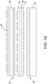
- one form of the present disclosureis a heater 50 that includes a base heater layer 52 having at least one heater circuit 54 embedded therein.
- the base heater layer 52has at least one aperture 56 (or via) formed therethrough for connecting the heater circuit 54 to a power supply (not shown).
- the base heater layer 52provides primary heating while a tuning heater layer 60 disposed proximate the heater layer 52 as shown provides for fine tuning of a heat distribution provided by the heater 50.
- the tuning layer 60includes a plurality of individual heating elements 62 embedded therein, which are independently controlled. At least one aperture 64 is formed through the tuning layer 60 for connecting the plurality of individual heating elements 62 to the power supply and controller (not shown).
- a routing layer 66is disposed between the base heater layer 52 and the tuning layer 60 and defines an internal cavity 68.
- a first set of electrical leads 70connects the heater circuit 54 to the power supply, which extend through the heater layer aperture 56.
- a second set of electrical leads 72connects a plurality of heating elements 62 to the power supply and extend through the internal cavity 68 of the routing layer 66, in addition to the aperture 55 in the base heater layer 52.
- the routing layer 66is optional, and the heater 50 could be employed without the routing layer 66 and instead having only the base heater layer 52 and the tuning heater layer 60.
- the tuning layer 60may alternately be used to measure temperature in the chuck 12.
- This formprovides for a plurality of area-specific or discreet locations, of temperature dependent resistance circuits.
- Each of these temperature sensorscan be individually read via a multiplexing switching arrangement, exemplary forms of which are set forth in greater detail below, that allows substantially more sensors to be used relative to the number of signal wires required to measure each individual sensor.
- the temperature sensing feedbackcan provide necessary information for control decisions, for instance, to control a specific zone of backside cooling gas pressure to regulate heat flux from the substrate 26 to the chuck 12.
- This same feedbackcan also be used to replace or augment temperature sensors installed near the base heater 50 for temperature control of base heating zones 54 or balancing plate cooling fluid temperature (not shown) via ancillary cool fluid heat exchangers.
- the base heater layer 50 and the tuning heater layer 60are formed from enclosing heater circuit 54 and tuning layer heating elements 62 in a polyimide material for medium temperature applications, which are generally below 250° C. Further, the polyimide material may be doped with materials in order to increase thermal conductivity.
- the base heater layer 50 and/or the tuning heater layer 60are formed by a layered process, wherein the layer is formed through application or accumulation of a material to a substrate or another layer using processes associated with thick film, thin film, thermal spraying, or sol-gel, among others.
- the base heating circuit 54is formed from Inconel ® and the tuning layer heating elements 62 are a Nickel material.
- the tuning layer heating elements 62are formed of a material having sufficient temperature coefficient of resistance such that the elements function as both heaters and temperature sensors, commonly referred to as "two-wire control.” Such heaters and their materials are disclosed in U.S. Patent No. 7,196,295 and pending U.S. patent application serial no. 11/475,534 , which are commonly assigned with the present application.
- various forms of the present disclosureinclude temperature, power, and/or thermal impedence based control over the layer heating elements 62 through knowledge or measurement of voltage and/or current applied to each of the individual elements in the thermal impedance tuning layer 60, converted to electrical power and resistance through multiplication and division, corresponding in the first instance, identically to the heat flux output from each of these elements and in the second, a known relationship to the element temperature.
- thesecan be used to calculate and monitor the thermal impedance load on each element to allow an operator or control system to detect and compensate for area-specific thermal changes that may result from, but are not limited to, physical changes in the chamber or chuck due to use or maintenance, processing errors, and equipment degradation.
- each of the individually controlled heating elements in the thermal impedance tuning layer 60can be assigned a setpoint resistance corresponding to the same or different specific temperatures which then modify or gate the heat flux originating from corresponding areas on a substrate through to the base heater layer 52 to control the substrate temperature during semiconductor processing.
- the base heater 50is bonded to a chuck 51, for example, by using a silicone adhesive or even a pressure sensitive adhesive. Therefore, the heater layer 52 provides primary heating, and the tuning layer 60 fine tunes, or adjusts, the heating profile such that a uniform or desired temperature profile is provided to the chuck 51, and thus the substrate (not shown).
- the coefficient of thermal expansion (CTE) of the tuning layer heating elements 62is matched to the CTE of the tuning heating layer substrate 60 in order to improve thermal sensitivity of the tuning layer heating elements 62 when exposed to strain loads.
- CTEcoefficient of thermal expansion
- Many suitable materials for two-wire controlexhibit similar characteristics to Resistor Temperature Devices (RTDs), including resistance sensitivity to both temperature and strain. Matching the CTE of the tuning layer heating elements 62 to the tuning heater layer substrate 60 reduces strain on the actual heating element. And as the operating temperatures increase, strain levels tend to increase, and thus CTE matching becomes more of a factor.
- the tuning layer heating elements 62are a high purity Nickel-Iron alloy having a CTE of approximately 15 ppm/°C, and the polyimide material that encloses it has a CTE of approximately 16 ppm/°C.
- materials that bond the tuning heater layer 60 to the other layersexhibit elastic characteristics that physically decouple the tuning heater layer 60 from other members of the chuck 12. It should be understood that other materials with comparable CTEs may also be employed while remaining within the scope of the present disclosure.
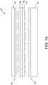
- the heater 80includes a base plate 82, (also referred to as a cooling plate), which in one form is an Aluminum plate approximately 16mm in thickness.
- a base heater 84is secured to the base plate 82, in one form using an elastomeric bond layer 86 as shown.
- the elastomeric bondmay be one disclosed in U.S. Patent No. 6,073,577 .
- a substrate 88is disposed on top of the base heater 84 and is an Aluminum material approximately 1mm in thickness according to one form of the present disclosure.
- the substrate 88is designed to have a thermal conductivity to dissipate a requisite amount of power from the base heater 84. Because the base heater 84 has relatively high power, without a requisite amount of thermal conductivity, this base heater 84 would leave "witness" marks (from the resistive circuit trace) on adjacent components, thereby reducing the performance of the overall heater system.
- a tuning heater 90is disposed on top of the substrate 88 and is secured to a chuck 92 using an elastomeric bond layer 94, as set forth above.
- the chuck 92 in one formis an Aluminum Oxide material having a thickness of approximately 2.5mm. It should be understood that the materials and dimensions as set forth herein are merely exemplary and thus the present disclosure is not limited to the specific forms as set forth herein.
- the tuning heater 90has lower power than the base heater 84, and as set forth above, the substrate 88 functions to dissipate power from the base heater 84 such that "witness" marks do not form on the tuning heater 90.
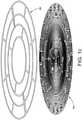
- the base heater 84 and the tuning heater 90are shown in greater detail in FIG. 1c , in which an exemplary four (4) zones are shown for the base heater 84, and eighteen (18) zones for the tuning heater 90.
- the heater 80is adapted for use with chuck sizes of 450mm, however, the heater 80 may be employed with larger or smaller chuck sizes due to its ability to highly tailor the heat distribution.
- the high definition heater 80may be employed around a periphery of the chuck, or in predetermined locations across the chuck, rather than in a stacked/planar configuration as illustrated herein. Further still, the high definition heater 80 may be employed in process kits, chamber walls, lids, gas lines, and showerheads, among other components within semiconductor processing equipment. It should also be understood that the heaters and control systems illustrated and described herein may be employed in any number of applications, and thus the exemplary semiconductor heater chuck application should not be construed as limiting the scope of the present disclosure.
- the base heater 84 and the tuning heater 90not be limited to a heating function. It should be understood that one or more of these members, referred to as a "base functional layer” and a “tuning layer,” respectively, may alternately be a temperature sensor layer or other functional member while remaining within the scope of the present disclosure.
- a dual tuning capabilitymay be provided with the inclusion of a secondary tuning layer heater 99 on the top surface of the chuck 12.
- the secondary tuning layermay alternately be used as a temperature sensing layer rather than a heating layer while remaining within the scope of the present disclosure. Accordingly, any number of tuning layer heaters may be employed and should not be limited to those illustrated and described herein.
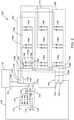
- the system 100includes a controller 110.
- the controller 110may be a control circuit or a microprocessor based controller.
- the controller 110may be configured to receive sensor measurements and implement a control algorithm based on the measurements.
- the controllermay measure an electrical characteristic of one or more of the thermal array elements.
- the controller 110may include and/or control a plurality of switches to determine how power is provided to each thermal element of the array based on the measurements.
- poweris provided to the array through a three-phase power input as denoted by reference numerals 112, 114, 116.
- the input powermay be connected to a rectifier circuit 118 to provide a positive direct current (DC) power line 120 and a negative DC power line 122.
- the powermay be distributed to the thermal array through six power nodes.
- the controller 110may be configured to control a plurality of switches, such that the positive power line 120 can be routed to any one of the six power nodes and the negative power line 122 can also be routed to any one of the plurality of power nodes.
- the power nodesare configured into two groups of nodes.
- the first group of nodesincludes power node 136a, power node 136b, and power node 136c.
- the second groupincludes power node 138a, power node 138b, and power node 138c.
- the thermal elementsare configured into a matrix arrangement with three groups of thermal elements and each group containing six thermal elements. However, as with each implementation described herein, more or fewer nodes can be used and , further, the number of thermal elements may be correspondingly increased or decreased with the number of nodes.
- the first group 160 of the thermal elementsare all connected to node 138a.
- the second group 170 of thermal elementsare all connected to power node 138b, while the third group 180 of thermal elements are all connected to power node 138c.
- the thermal elementmay be heater elements.
- the heater elementsmay be formed of an electrically conductive material with, for example, a temperature dependent electrical resistance. More specifically, the thermal elements may be heater elements with an electrical characteristic, such as a resistance, capacitance, or inductance, that correlates to temperature. Although, the thermal elements may also generally be classified as dissipative elements, such as resistive elements.
- the six thermal elementsare configured into pairs of thermal elements.
- the first pair of thermal elements 146aincludes a first thermal element 164 and a second thermal element 168.
- the first thermal element 164is configured in electrical parallel connection with the second thermal element 168.
- the first thermal element 164is in electrical series connection with a unidirectional circuit 162.
- the unidirectional circuit 162may be configured to allow current to flow through the thermal element 164 in one direction and not in the opposite direction. As such, the unidirectional circuit 162 is shown in its simplest form as a diode.
- the first unidirectional circuit 162is shown as a diode with the cathode connected to node 136a and the anode connected to node 138a through thermal element 164.
- the second unidirectional circuit 166is shown as a diode with a cathode connected to node 138a through the second thermal element 168 and an anode connected to node 136a, thereby illustrating the unidirectional nature of the first unidirectional circuit 162 being opposite to the second unidirectional circuit 166.
- a diodeas a unidirectional circuit may only work for a one volt power supply, however, various other circuits may be devised including for example, circuits using silicon controlled-rectifiers (SCR's) that work for higher power supply voltages.
- SCR'ssilicon controlled-rectifiers
- Such implementations of unidirectional circuitsare described in more detail later, but could be used in conjunction with any of the implementations described herein.
- the second thermal element 168is in electrical series connection with a second unidirectional circuit 166, again in its simplest form shown as a diode.
- the first thermal element 164 and the first unidirectional circuit 162are parallel with the second thermal element 168 and the second unidirectional circuit 166 between the power node 138a and power node 136a. Accordingly, if the controller 110 applies a positive voltage to node 136a and a negative voltage to node 138a, power will be applied across both the first thermal element 164 and the second thermal element 168 of the first pair 146a.
- the first unidirectional circuit 162is oriented in an opposite direction of the second unidirectional circuit 166.
- the first unidirectional circuit 162allows current to flow through the first thermal element 164 when a positive voltage is applied to node 138a and a negative voltage is applied to node 136a, but prevents current from flowing when a positive voltage is provided to node 136a and a negative voltage is provided to node 138a.
- currentis allowed to flow through the second thermal element 168, however, current flow through the second thermal element 168 is prevented by the second unidirectional circuit 166 when the polarity is switched.
- each pair of thermal elements within a groupis connected to the different power node of the first group of power nodes 136a, 136b, 136c. Accordingly, the first pair of thermal elements 146a of the first group 160 is connected between node 136a and node 138a. The second pair of thermal elements 146b is connected between power node 136b and power node 138a, while the third pair 146c of thermal elements of group 160 is connected between power node 136c and power node 138a.
- the controller 110may be configured to select the group of elements by connecting power node 138a to supply power or return then the pair of thermal elements (146a, 146b, 146c) may be selected by connecting one of the nodes 136a, 136b, or 136c, respectively, to supply power or return. Further, the controller 110 may select to provide power to the first element of each pair or the second element of each pair based on the polarity of the voltage provided between node 138a and nodes 136a, 136b, and/or 136c.
- the second group of thermal elements 170are connected between node 138b of the second group of nodes, and node 136a, 136b, and 136c.
- the first pair 146d of thermal elements of group 170may be selected using power node 136a
- the second pair 146e and the third pair 146f of thermal elements of group 170may be selected by node 136b and 136c, respectively.
- the second group of thermal elements 180are connected between node 138c of the second group of nodes, and node 136a, 136b, and 136c.
- the first pair 146g of thermal elements of group 180may be selected using power node 136a, while the second pair 146h and the third pair 146i of thermal elements of group 170 may be selected by node 136b and 136c, respectively.
- the controller 110manipulates a plurality of switches to connect the positive power line 120 to one of the first group of power nodes and the negative power line 122 to the second group of power nodes or, alternatively, connects the positive power line 120 to the second group of power nodes and the negative power line 122 to the first group of power nodes.
- the controller 110provides a control signal 124 to a first polarity control switch 140 and a second polarity control switch 142.
- the first polarity control switch 140connects the first group of power nodes to either the positive power supply line 120 or the negative power supply line 122
- the second polarity switch 142connects the second group of power nodes to the positive power supply line 120 or the negative power supply line 122.
- the controller 110provides control signals 126 to the first group power switches 130, 132, and 134.
- the switches 130, 132, and 134connect the output of switch 140 (the positive supply line 120 or the negative supply line 122) to the first node 136a, the second node 136b, and the third node 136c, respectively.
- the controller 110provides control signals 128 to the second group power switches 150, 152, and 154.
- the switches 150, 152, and 154connect the output of switch 142 (the positive supply line 120 or the negative supply line 122) to the first node 138a, the second node 138b, and the third node 138c, respectively.
- a multi-parallel thermal array system 200is provided.
- the system 200includes a control system 210.
- the control systemmay include a microprocessor, switches, and other discrete components similar to those described throughout the application to implement the logic described herein.
- the thermal elementsare arranged in a multi-parallel fashion across pairs of power nodes. For the implementation shown, six power nodes (212, 214, 216, 218, 220, 222) are provided. Further, each thermal element is connected between a pair of power nodes. More specifically, each thermal element is connected between a different pair of power nodes. As such, each node has one thermal element connected between itself and each other power node.
- thermal element 230is connected between node 212 and node 222
- thermal element 232is connected between node 212 and node 220
- thermal element 234is connected between node 212 and node 21
- thermal element 236is connected between node 212 and node 216
- thermal element 238is connected between node 212 and node 214.
- node 212is connected to each of the other nodes 214, 216, 218, 220, and 222 through a thermal element (230, 232, 234, 236, or 238).
- thermal element 240is connected between node 214 and node 222
- thermal element 242is connected between node 214 and node 220
- thermal element 244is connected between node 214 and node 218,
- thermal element 246is connected between node 214 and node 216. It is noted that the thermal element connected between node 214 and node 212 has already been identified as thermal element 238.
- thermal element 250being connected between node 216 and node 222
- thermal element 252being connected between node 216 and node 220
- thermal element 254being connected between node 216 and node 218
- thermal element 260being connected between node 218 and node 222
- thermal element 262being connected between node 218 and node 220
- thermal element 270being connected between node 220 and node 222.
- the controller 210is configured to provide a power connection, a return connection, or an open circuit to each node.
- the multi-parallel topologyis significantly different from the matrix topology provided in FIG. 2 .
- the multi-parallel topologyprovides that the thermal element network be considered in whole with regard to power distribution for heating as well as understanding the interaction of all elements for thermal sensing. For example, if a supply power is provided to node 212 and a return connection is provided to node 222, the primary power path would be through thermal element 230. However, secondary paths would exist through each of the other elements within the network back to node 222.
- the controller 210when providing power and return to any configuration of nodes must consider the power being provided to the thermal element of the primary path, as well as, the power being provided to all the other elements through the secondary paths. This task can be significantly complex based on each thermal element having different characteristics either by design, environmental influences, or manufacturing tolerances.
- the control schememay be employ six (6) wires and fifteen elements (15) without the use of switching circuits having SCRs, diodes, and other elements as set forth above.
- wiresare selectively connected to power, return, or are left open-circuit, using sequences of these combinations for specified periods of time, in order to produce a desired average heating distribution.
- one combinationcould be to connect A and B to power, connect C and D to return, and leave E and F open-circuit; another combination could be to connect A and C to power, connect D to return, and leave B, E and F open-circuit.
- These combinations or modesare then applied in sequence to the tuning layer heating elements for varying periods of time, e.g., a first mode is applied for a first time t 1 , a second mode is applied for a second time t 2 , and so on, such that the resulting timed sequence produces the desired average heating distribution in the tuning layer heater.
- timing sequence time intervalsare used that are much shorter than the thermal time constant of the heater so that temperature ripple in the heater is kept to a sufficiently low level.
- P Eis a vector of Power (heat flux) output from the elements.
- the number of multiparallel modes(3 N - 2 N+1 - 1)/2 (non-redundant).
- the [PxM] matrixis underdetermined and likely to be ill-conditioned if the full open-circuit inclusive matrix is used and produces a mode vector that is highly error prone and difficult to implement due to the number of modes that must be produced in a given time window.
- a solutionis not always possible for all desired power vectors.
- Complexity and errorsmay be reduced by selecting a subset of modes chosen based on matrix condition.
- One method for evaluating matrix condition of a selected subset of modesis to perform a singular value decomposition on subsets of the [PxM] matrix, comparing subsets against each other and selecting the set with the smallest ratio of largest to smallest non-zero singular values. Only non-negative modes can be used because power can only be added to the system, so this matrix subset [PxM R ] can then be used to solve a the non-negative least squares problem min Modes ⁇ PxM R • Modes ⁇ P E ⁇ 2 2 where Modes ⁇ 0.
- the thermal array system 300includes a control system 310.
- the control system 310may include a microprocessor, switches, and other discrete components similar to those described throughout the application to implement the logic described herein.
- the thermal elementsare arranged in a multi-parallel fashion across pairs of power nodes. Being bidirectional, twice the number of thermal elements are able to be controlled with the same number of nodes. For the embodiments shown, six power nodes (312, 314, 316, 318, 320, 222).
- each pair of thermal elementis connected between a pair of power nodes, where each thermal element of the pair of thermal elements have a different polarity. More specifically, each pair of thermal element is connected between a different pair of power nodes. As such, each node has one pair of thermal element connected between itself and each other power node, where the thermal elements in each pair are activated by a different polarity of supply power.
- thermal element pair 350is connected between node 312 and node 322.
- the thermal element pair 350includes a first thermal element 332 and a second thermal element 334.
- the first thermal element 332is configured in electrical parallel connection with the second thermal element 334.
- the first thermal element 332is in electrical series connection with a unidirectional circuit 330.
- the unidirectional circuit 330may be configured to allow current to flow through the thermal element 332 in one direction and not in the opposite direction. As such, the unidirectional circuit 330 is shown in its simplest form as a diode.
- the first unidirectional circuit 330is shown as a diode with the cathode connected to node 312 and the anode connected to node 314 through thermal element 332.
- the second unidirectional circuit 336is shown as a diode with a cathode connected to node 314 and an anode connected to node 312 through the second thermal element 334, thereby illustrating the unidirectional nature of the first unidirectional circuit 330 being opposite to the second unidirectional circuit 336.
- the first unidirectional circuit 330allows current to flow through the first thermal element 332 when a positive voltage is applied to node 322 and a negative voltage is applied to node 312, but prevents current from flowing when a positive voltage is provided to node 312 and a negative voltage is provided to node 322.
- currentis allowed to flow through the second thermal element 334, however, current flow through the second thermal element 334 is prevented by the second unidirectional circuit 336 when the polarity is switched.
- Thermal element pair 352is connected between node 312 and node 320
- thermal element pair 354is connected between node 312 and node 318
- thermal element pair 356is connected between node 312 and node 316
- thermal element pair 358is connected between node 312 and node 314.
- node 312is connected to each of the other nodes 314, 316, 318, 320, and 322 through a thermal element pair (350, 352, 354, 356, or 358).
- thermal element pair 360is connected between node 314 and node 322
- thermal element pair 362is connected between node 314 and node 320
- thermal element pair 364is connected between node 314 and node 318
- thermal element pair 366is connected between node 314 and node 316. It is noted that the connected between node 314 and node 312 has already been identified through thermal element pair 358.
- thermal element pair 370being connected between node 316 and node 322
- thermal element pair 372being connected between node 316 and node 320
- thermal element pair 374being connected between node 316 and node 318
- thermal element pair 380being connected between node 318 and node 322
- thermal element pair 382being connected between node 318 and node 320
- thermal element pair 390being connected between node 320 and node 322.
- the controller 310is configured to provide a power connection, a return connection, or an open circuit to each node.
- the multi-parallel topologyprovides that the thermal element network be considered in whole with regard to power distribution for heating as well as understanding the interaction of all elements for thermal sensing. For example, if a supply power is provided to node 312 and a return connection is provided to node 322, the primary power path would be through thermal element pair 350. However, secondary paths would exist through each of the other elements within the network back to node 322. As such, the controller 310 when providing power and return to any configuration of nodes must consider the power being provided to the thermal element of the primary path as well as the power being provided to all the other elements through the secondary paths.
- the system 400includes a controller 410 which controls a plurality of power nodes.
- the controller 410controls six power nodes 412, 414, 416, 418, 420, and 422.
- each nodeis connected to each of the other nodes through a thermal element.
- each elementis connected to each other element through two thermal elements, where one of the thermal elements connects the pair of nodes in a first polarity and the second thermal element connects the pair of elements in the opposite polarity.
- each unidirectional circuit 430is shown as a combination of elements including a SCR 432, a diode 436 and a zener diode 434.
- the unidirectional element 430is in electrical series connection with each thermal element, for example, thermal element 438.
- the thermal element 438 and the unidirectional circuit 430are in electrical series connection between node 414 and node 412. If a positive supply voltage was provided to node 414 and a return was provided to node 412, current would be allowed to flow through the thermal element 438 and the SCR 432.
- the thermal element 438is connected between node 414 and the anode of SCR 432.
- the anode of SCR 432is connected to the thermal element 438 and the anode of diode of 436.
- the cathode of diode 436is connected to the cathode of zener diode 434. Further, the anode of zener diode 434 is connected to the source of the SCR 432 and node 412.
- the SCR 432fires when there is a gate current to the SCR.
- the SCRreceives gate current when current flows in the direction of the diode 436 and exceeds the voltage gap of the zener diode 434.
- the gate current of the SCRcould be triggered by another configuration of devices. Further, the triggering could be my means other than electrical, for example optical or magnetic.
- a thermal configurationsuch as 440 including a thermal element and unidirectional circuit are provided between each node for example, node 414 and node 412.
- two thermal configurations with opposite polaritiesmay be connected between each pair of nodes of the plurality of power nodes.
- thermal configuration 440is connected between node 414 and node 412, but in an opposite polarity than unidirectional circuit 430.
- the cathode of SCR 433is connected to node 414 while the cathode of SCR 432 is connected to node 412. Therefore, each will conduct only in opposite polarity conditions.
- each nodemay be connected to a pair of switches, as denoted by reference numeral 492.
- the pair of switchesmay be transistors, for example field effect transistors (FETs) in a half-bridge configuration.
- the first transistor 490may be a low control switch connecting the node 412 to a return voltage when activated, while the second transistor 491 may be a high control switch connecting the node 412 to a supply voltage when activated.
- the first transistor 490may have a source connected to a negative voltage line through a shunt 498 and a drain connected to one of the plurality of nodes.
- the other transistor 491may have the source connected to the node 412 and a drain connected to a positive voltage node.
- first transistor 490 and the second transistor 491may each have a gate connected to control circuitry or a microprocessor implementing control logic. It is also noted that the control system switching arrangement (e.g. half bridge configuration) can be applied to any of the topologies applied herein.
- Each other nodealso has a corresponding pair of transistors. Specifically, node 414 is connected to transistor pair 493, node 416 is connected to transistor pair 494, node 418 is connected to transistor pair 495, node 420 is connected to transistor pair 496 and node 422 is connected to transistor pair 497. While the control circuit 410 may provide a combination of return, supply power, or open circuit to each of the nodes independently, at least one node will be connected to a supply voltage and at least one node will be connected to a return. Various combinations of supply power, return (e.g. ground), and open circuit conditions can be provided to the nodes. Each combination is a possible mode for powering the thermal element array.
- a currentwill flow through the shunt 498 and may be measured by the control circuit 410.
- a microprocessormay measure the voltage across the shunt or the current through the shunt to determine electrical characteristics of the thermal element array, such as the network resistance.
- the network resistancemay be used for controlling the amount of time each mode is applied, or for modifying other circuit parameters such as the input voltage, the duty cycle, current, or other electrical characteristics.
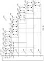
- a thermal array system 500 with addressable switchesis provided.
- the controller 510may be connected to a positive node 514 and negative node 516.
- a power source 512is connected between the positive node 514 and the negative node 516.
- Each thermal elementis connected in electrical series connection with an addressable switch between the positive node 514 and the negative node 516.
- Each addressable switchmay be a circuit of discreet elements including for example, transistors, comparators and SCR's or integrated devices for example, microprocessors, field-programmable gate arrays (FPGA's), or application specific integrated circuits (ASIC's).
- Signalsmay be provided to the addressable switches 524 through the positive node 514 and/or the negative node 516.
- the power signalmay be frequency modulated, amplitude modulated, duty cycle modulated, or include a carrier signal that provides a switch identification indicating the identity of the switch or switches to be currently activated.
- various commandsfor example, a switch on, switch off, or calibration commands could be provided over the same communication medium.
- each thermal element 522 and addressable switch 524form an addressable module 520 connected between the positive node 514 of the negative node 516.
- Each addressable switchmay receive power and communication from the power lines and, therefore, may also separately be connected to the first node 514 and/or the second node 516.
- Each of the addressable modulesmay have a unique ID and may be separated into groups based on each identifier. For example, all of the addressable modules (520, 530, 532, 534, 536, 538, 540, 542, and 544) in the first row may have a first or x identifier of one. Similarly, all of the addressable modules (546, 548, 550, 552, 554, 556, 558, 560, 562) in the second row may have an x identifier of two, while the modules (564, 566, 568, 570, 572, 574, 576, 578, 580) in the third row have an x identifier of three.
- the first three columns 582 of addressable modulesmay have a z identifier of one.
- the second three columns 584may have a z identifier of two, while the third three columns 586 may have a z identifier of three.
- each addressable modulehas a unique y identifier within each group. For example, in group 526, addressable module 534 has a y identifier of one, addressable module 536 has a y identifier of two, and addressable module 538 has a y identifier of three.
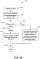
- a method 600is provided for controlling the thermal element array.
- the methodstarts at block 610.
- the controllercalculates the set points for each thermal element of the array. For example, resistance set points may be set for each thermal element such that a measured resistance for that element can be used as a trigger to stop providing power to that element.
- the time window for each thermal elementis calculated. The time window may be the time allotted to power a particular thermal element.
- the controllermay remain dormant for the remainder of the time window or may directly move to the next window to power the next thermal element.
- it may be desirable to have a minimum wait time for each thermal elementsuch that power is not constantly provided to the system for measurement purposes, thereby heating elements beyond what is necessary for the heating application.
- the controllerdetermines if the end of the time window has been reached for the current thermal element. If the end of the time window had been reached for the current element, the method follows line 620 to block 622. In block 622, the controller increments to the next thermal element within the array and proceeds to block 616 where the process continues. If the end of the time window has not been reached the method follows line 618 to block 624. In block 624, the controller may simultaneously provide power to the thermal element and measure electrical characteristics of the thermal element. In block 626, the controller determines if the thermal element has exceeded the thermal element set point based on the measured characteristics. If the set point has been exceeded, the method may wait until the timing window is complete or, after some delay, proceed along the line 628 to block 622. In block 622, the thermal element is incremented to the next thermal element and the process proceeds to block 616. If the thermal element has not exceeded the set point based on the measured characteristics, the process follows line 630 block 616 where the process continues.
- FIG. 6Ba timing diagram illustrating one scenario of the method 600 is provided.
- the first elementis considered during the first time window 650.
- the resistance of the first elementis denoted by line 654.
- the resistance of the thermal elementmay correlate to the temperature of the thermal element.
- the set point for the first thermal elementis denoted by line 652.
- the temperature of the thermal elementincreases over the first time window 650 as power is applied to the thermal element.
- the first thermal elementis too cold and does not reach the set point 652, before the first time window 650 elapses.
- the controllerprovides power to the second element to measure the resistance 658.
- the temperature and, therefore, the resistance 658is immediately higher than the element set point 660. Since the resistance is too high, it is determined that the element is too hot. Therefore, the second thermal element is immediately turned off for the remainder of the second time window 656.
- the controllermay remain dormant for the remainder of the second time window 656 or may, after a predefined time delay, move to the third time window 662.
- a third elementis powered and monitored.
- the resistance of the third element 664starts below the set point of the third element 666.
- the resistanceincreases as denoted by line 664 until the resistance reaches the set point of the third element 666 as denoted at point 668.
- the elementis turned off and the controller may remain dormant during the rest of the third time window 662.
- the first time windowmay repeat as denoted by reference numeral 670.
- the resistance 672 of the first elementstarts below the first element set point 674.
- the first elementhas warmed from the last starting point of time window 650.
- the resistance 672 of the first elementeventually reaches the first set point 674 at point 676 before the end of the time window 670.
- the first elementhaving retained some of its energy from its last activation, the applied power was sufficient to reach the set point and turn off before the end of time window 670. Therefore, the controller may remain dormant for the rest of time window 670 or after a predefined time delay leading directly to the time window for the second element.
- the various time windowswill then repeat based on the condition of each thermal element and environmental influences.
- the control methodshows the behavior of three positive TCR tuning layer heating elements under various thermal conditions. Although other implementations may used, for example negative TCR heating elements in which case the setpoints would be approached from a higher resistance level.
- the method of controlis accomplished by calculating the resistance of each element during the time window assigned for that element utilizing voltage and/or current information obtained when the element is energized. It should be recognized that the element resistance may be inferred by measuring only current or voltage as long as the power is supplied by, respectively, a known voltage or current source. Energizing a heating element increases its temperature, and thus its resistance rises while it is actively powered. Utilizing previously obtained calibration information, the sampled and active resistance is compared to a previously assigned set point for that heating element.
- the elementAs long as the resistance remains lower than the assigned set point, the element remains energized until the end of the assigned time window; or, if the element resistance is above or rises above its target set point resistance, the element is immediately turned off and remains off for the remainder of the assigned time window. Each element becomes active in sequence, and then the cycle begins again and repeats continuously.
- Time windowsneed not be of fixed duration. It is sufficient that the system dissipates enough energy from each element such that the minimum "On-time” required for the first measurement does not contribute more energy than can be dissipated by the system before that element again becomes active, and that sufficient energy can be supplied during the maximum "On-time” such that the average temperature of each element can be increased for the control system to assume control during its active window. Steady-state control is achieved when all heating elements in the tuning layer consistently reach their individual set points during their assigned time windows. Efficiency of control is achieved by choosing a minimum set point range for the tuning heater layer, sufficient supplied power, short time window duration, fast sampling, and the minimum required number of elements.
- FIG. 7aanother method for controlling the thermal array is provided.
- the methodstarts in block 710, where the resistance set points are calculated for each mode, along with a power command for each thermal element.
- the time period for each modeis determined.
- the modeis set to a first mode or initial mode.
- the controllerapplies the current mode to the heater array.
- the controllerwaits for the end of the time period continuing to provide power as defined by the mode.
- the modeis incremented.
- the controllerdetermines if the current mode is the last mode of the sequence. If the current mode is not greater than the total number of modes in the sequence, the method follows line 724 to block 716, where the current mode is applied and the method continues.
- the methodfollows line 726 to block 728.
- the controllerdetermines whether the system needs to determine temperature at the thermal elements, for example by measuring characteristics of the thermal elements.
- the control systemmay measure the thermal characteristics based on various algorithms including the predetermined number of sequences, based on a time period, or based on identified environmental characteristics. If the temperature does need to be measured, the method follows line 734 to block 736, where the temperatures are determined as described elsewhere in this application. The method then follows line 738 to block 732. Alternatively, if the temperatures do not need to be measured in block 728, the method flows along line 730 to block 732.
- the controllerwaits until the allotted sequence time has passed. It may be important for the system to wait for the allotted sequence time, otherwise additional heat may be added to the system faster than anticipated which may compromise stability of the algorithm. The method then proceeds to block 740.
- the controllerdetermines whether the power command has changed, based on the measurement. Accordingly, an algorithm such as a PID algorithm adjusts the power command, as denoted in block 742 based on the measurement performed by the controller in block 736.
- the algorithm in block 742may determine the adjusted power command and provide information that the power command has changed to block 740. If the power command has changed in block 740, the method follows line 746 to block 712 where the time periods for each mode are recomputed. The method then continues. If the system characteristics have not changed, the method follows line 744 to block 714 where the control system resets to the first mode and the method continues.
- a multi-parallel arraymay be comprised of an n-wire power interface, connected to a number of heaters such that every possible pairing of control wires has a single heater connected between them. It can be easily shown that the number heaters that can be connected in this way is equal to n ( n -1)/2 .
- heater resistancesare all one ohm and control lines are driven at 1 volt, zero volts, or are open-circuited (high impedance).
- the systemcan be scaled using the equations presented here to a system with other voltages and resistances.
- This methodpartitions the control into two parts, that is, a constant part and a deviation part, in which the constant part is equal for all heaters, and the deviation part is equal and symmetric for all heaters.
- Other control partitionsare be possible that can provide for greater flexibility in the control. For example, a system might be partitioned into two different constant parts and a single deviation part, allowing for two distinct control zones at different mean power levels. Also, the system might be partitioned into a single constant part and two deviation parts to give greater range of control in a subset of the heaters. Note that regardless of the partitioning, it is possible to apply control vectors where the constraints on c can be violated, and yet control is possible even though stable control cannot be guaranteed.
- a mode tablemay be constructed for the system. Power may be computed for each power supply and heater, for each unique combination of power application to the array. These values may be stored in the mode table.
- Mode #11has ground connected at V1 and V4 (producing zero power), power connected at V3 (producing 2.67 watts), and V2 is open-circuit.
- a matrix Acomprised of heater powers for a subset of modes. This matrix must be at least rank n, where n is the number of heaters in the system.
- nis the number of heaters in the system.
- One optimal selection of modesresults in A having low matrix condition number, maximum average total power, maximum available power deviation, and a minimal number of modes.
- this matrixis not a minimal-row solution, nor does it have the lowest condition number of other solutions, but it does represent a controllable system.
- Average heater power pcan be controlled using a generalized duty cycle vector d , where and where the modes m l are applied to the array for times so that
- the equation for the duty cyclesmay be solved as a function of c using to get:
- a time quantum ⁇may be chosen that can be implemented in the controller, e.g., one microsecond. Also choose a base control loop period T for the system that is sufficiently smaller than the thermal time constant of the heater system, e.g, 1 second.
- a time period(e.g. in the form of a duty cycle) may be defined as and substitute in the equation for d to get the following:
- This equationcan be implemented in the controller as a pair of constant coefficient matrices along with a function that computes the duty cycles d c from the control vector c (which is a vector of floating point values).
- a method 800 for measuring resistancesis provided.
- the method 800may be particularly useful with the method of FIG. 7a (e.g. block 736).
- the characteristicfor example, may be assigned a null vector and the mode may be set to the first mode.
- the controllerapplies the active mode to the thermal array.
- the controllermeasures the amount of current provided into the array for the active mode.
- the controllerindexes to the next mode to make it the active mode.
- the controllerdetermines if the active mode is greater than the total number of modes. If the active mode is not greater than the total number of modes, the method follows line 820 to block 812, where the next mode is applied to the thermal array.
- the methodfollows line 822 to block 824.
- the controllerdetermines the current for each thermal element based on the current applied to the active mode and the relationship of the resistances.
- the methodthen proceeds to block 826, where the resistance for each thermal element is determined based on the voltage provided to the system and the current that is allocated to each thermal element. From the resistance measurement, the controller can then determine a temperature of each thermal element according to a temperature resistance relationship that is stored for each thermal element.
- the systemmay measure the current applied to the mode to calculate the resistances of each thermal element.
- the systemmay also or alternatively measure other parameters such as the voltage at each of the nodes. Obtaining additional measurements can help to over constrain the relationship and a least squares fit may be used to determine the resistances. Over constraining the relationship may reduce the error in the calculations and provide more reliable resistance values for each thermal element. While this may be applied to the batch processing method of FIG. 7a and 7b , this could equally be applied to the indexing method described in relation to FIG 6a and 6b .
- the resistancemay be used to calculate temperature information at the thermal element
- the power provided to the thermal element and/or thermal array as a wholecan be used to calculate heat flux at the thermal elements.
- this informationmay be used as feedback, for example changing process parameters for a power setpoint.
- these characteristicsmay be used as feedback to an external process, for example, to control other environmental variables such as processing time or other process characteristics in manufacturing processes.
- One examplecould include adjusting processing time in the semiconductor manufacturing process to increase chip yield.
- Another examplecould include providing a system diagnostic for system degradation.
- the thermal elementacts as just a heater.
- the thermal elementsmay act as heaters and thermal sensors, or even in other implementations not part of the invention just as thermal sensors.
- the sensingmay be accomplished with a low voltage supply and/or a low power supply (e.g. short time period).
- the thermal arraymay be powered with a low amount of power to acquire the measurement without significantly disturbing the temperature of the thermal element.
- the thermal arraymay be powered with a voltage capable of causing less than 5% change in temperature for the temperature being measured during the time period applied.
- a low average poweris provided by a pulse power provided for less than one second.
- the controllermay create an alert based on the measured resistance (temperature) and/or power (heat flux) of each thermal element or a combination of thermal elements.
- the alertmay take many forms including a visual alert, audible alert, a control signal, a message (e.g. a text or email).
- a temperature measurement arraymay be enabled. Multiple thermal elements can be used as RTD sensors to measure with fewer electrical connections (nodes) by using a single integrated measurement system to compute the temperature for an entire array of sensors. Through rapid sequential measurements of low power applied in various combinations to one or more nodes (called Power Modes), all sensor resistances can be computed and converted into temperature. Further, it is noted that different modes may be used for powering than the modes that are used for measuring the thermal array.
- a Power Mode matrixis defined of size iModes x nNodes, which holds all combinations of each node powered with V+ or 0, but where the last node is always 0 (e.g. return or ground). If we normalize V+ to equal 1, then the Power Mode Matrix is just a binary table (because nodes must be either 0 or 1).
- a Routing matrix [R]may then be formed from the absolute difference between all node pairs for each Power Mode in [M] . This results in [R] of size iModes x nSensors which is not square for N>3 and not optimum for N>5. Using a subset of available modes the matrix condition of [R] for N>5 can be reduced, which may reduce the time of calculation and calculation error. For N>5, a minimum condition [R] is achieved by using only modes of [M] where two nodes are simultaneously active and where N-2 nodes are simultaneously active.
- [i M ]is a vector of individual measurements of total current into the sensor array for a each Power mode; and [i s ] is a vector of the equivalent sensor currents if the sensors were individually driven with no cross coupling. This procedure works as long as sensor resistances remain substantially constant throughout the time it takes to cycle through all modes in the set.
- TTemperature Coefficient of Resistance
- g 0 and g Tcan be extracted for known V; or if on a per-node basis, V in the baseline measurements is the same as V for the unknown temperature measurements, the element-wise ratio of the current vectors can be substituted directly into the equation above. Note: There is no restriction for baseline conductance variations in the first measurement or temperature variation between sensors in the second measurement.
- a method 900is provided in FIG. 9a for calibrating the array and a method 950 is provided in FIG. 9b for calculating target set points.
- the method 900 and the method 950may be particularly useful with the indexed control method of FIG. 6a (e.g. block 612) and the batch control method of FIG. 7a (e.g. block 710).
- the method 900begins in block 910.
- the controllerfixes the array temperature to a base line temperature, for example 25°C.
- the controllerdetermines whether the control process is controlling individual elements or if the elements are configured into a multi-parallel arrangement and are being controlled in a batch. If the elements are being measured in a batch, the method follows line 916 to block 918.
- a batch measurement procedurefor example as described with regard to FIG. 8 , may be used to gather batch measurements and transform the batch measurements to the individual element characteristics, which are then stored in a calibration baseline vector [R0]. The method then follows line 924 to block 926 where the method ends.
- the methodflows along line 920 to block 922.
- the individual element characteristicsare measured directly and stored in a calibration baseline vector [R0] as denoted by block 922.
- the methodthen proceeds to block 926 where the method ends.
- the resistancescould be manually measured for instance with an ohm meter.
- Method 950begins in block 943.
- an operatorprovides temperature set points for each element or mode, then the method proceeds to block 946.
- the controllercalculates the element temperature above the base line temperature and stores the difference for each element in a vector.
- the controllerapplies the temperature coefficient of resistance (TCR) to the stored vectors to generate an element target resistance vector.
- TCRtemperature coefficient of resistance
- the methodthen follows to block 930. If the thermal element array is a bidirectional array, the method follows line 940 to block 938. If the thermal element array is a multi-parallel array, the method follows line 932 to block 934. In block 934, the element target resistance vector is transformed into an array target resistance vector for each unique power mode.
- the methodthen follows line 936 to block 938 where the target resistances may be converted to target voltages or target currents based on the system voltages and currents.
- the methodthen proceeds to block 942 where the vector of target voltages or currents corresponding to each power mode is the output of the target setpoint calculation method.
- the methodends in block 948.
- the thermal elementsmay be heating elements made from high TCR materials so the heater control algorithm may be used, but without the diodes or SCRs. Nodes are powered sequentially with one source and one return, leaving the other nodes floating. This provides one dominant current path for control if the resistances of the thermal elements are substantially similar. However, the dominant current path is in parallel with one or more secondary paths of two or more heating elements in series.
- the secondary pathways in this systemcan be likened to cross coupling terms of a multiple-in/multiple-out control system. For good control the cross coupling terms should not dominate the system, for instance, by keeping the heating element resistances similar to each other.
- nPairModes x nNodesmay be definded, where, for each Mode (row) a '1' represents current flowing into one Node (column), '-1' represents current flowing out of another node, and '0' represents a floating node. Note that the number of PairModes equals the number of heating elements.
- a Vector [G] and a square Node matrix [GN]may be defined from heating element resistances:
- the baseline (e.g. 25°C) resistances of the heating elementsmay be obtained, either by independent measurement or by the method outlined above with regard to FIG 8 .
- the target resistances of each of the heating elements at their target temperaturecan be established to serve as the control points. It is recommended, where possible, that the target resistances at temperature be within ⁇ 30% of the mean to limit cross-coupling.
- the previously defined Conductance Node Matrix [GN]may be computed next.
- (nNodes-1) sub-matricies of [GN]can be created by eliminating one row-column starting with row-column 2.
- These matriciesrepresent the systems where the deleted row-column number is the grounded node of [M].
- nNodes-1 current vectorscan be created with '1' in each of the available bins and '0' in the others.
- I 11 0 0 T
- I 20 1 0 T
- I 30 0 1 T
- the maximum from each Voltage vectormay be retained and assemble into a new Vector [V n ] in the order of the Mode Matrix [M] , where the current vector is represented by the '1', and [GN] n is represented by '-1' for the eliminated row column.
- the control loopmay be closed for each mode by sequentially applying current source and sink to a mode pair defined by [M] , measuring the resulting voltage across that pair while leaving power applied until the measured voltage converges to the target voltage for that mode, or until a previously defined 'time-out' requires sequencing to the next mode pair.
- Target Voltagesare per amp of current applied. Too much current causes divergence, too little current prevents closed loop control.
- the convergence region for poweris controlled by the ratio of minimum On-Time to Time-Out.
- the computer system 1100includes a processor 1110 for executing instructions such as those described in the methods discussed above.
- the instructionsmay be stored in a computer readable medium such as memory 1112 or storage devices 1114, for example a disk drive, CD, or DVD.
- the computermay include a display controller 1116 responsive to instructions to generate a textual or graphical display on a display device 1118, for example a computer monitor.
- the processor 1110may communicate with a network controller 1120 to communicate data or instructions to other systems, for example other general computer systems.
- the network controller 1120may communicate over Ethernet or other known protocols to distribute processing or provide remote access to information over a variety of network topologies, including local area networks, wide area networks, the Internet, or other commonly used network topologies.
- dedicated hardware implementationssuch as application specific integrated circuits, programmable logic arrays and other hardware devices, can be constructed to implement one or more of the methods described herein.
- Applicationsthat may include the apparatus and systems of various embodiments can broadly include a variety of electronic and computer systems.
- One or more embodiments described hereinmay implement functions using two or more specific interconnected hardware modules or devices with related control and data signals that can be communicated between and through the modules, or as portions of an application-specific integrated circuit. Accordingly, the present system encompasses software, firmware, and hardware implementations.
- any of the topologies describedmay be used with any of the processing methods. Additionally, any the features described with respect to one topology or method may be used with the other topologies or methods.
- the methods described hereinmay be implemented by software programs executable by a computer system.
- implementationscan include distributed processing, component/object distributed processing, and parallel processing.
- virtual computer system processingcan be constructed to implement one or more of the methods or functionality as described herein.
- computer-readable mediumincludes a single medium or multiple media, such as a centralized or distributed database, and/or associated caches and servers that store one or more sets of instructions.
- computer-readable mediumshall also include any medium that is capable of storing, encoding or carrying a set of instructions for execution by a processor or that cause a computer system to perform any one or more of the methods or operations disclosed herein.
Landscapes
- Engineering & Computer Science (AREA)
- Manufacturing & Machinery (AREA)
- Condensed Matter Physics & Semiconductors (AREA)
- General Physics & Mathematics (AREA)
- Computer Hardware Design (AREA)
- Microelectronics & Electronic Packaging (AREA)
- Power Engineering (AREA)
- Physics & Mathematics (AREA)
- Control Of Resistance Heating (AREA)
- Container, Conveyance, Adherence, Positioning, Of Wafer (AREA)
- Drying Of Semiconductors (AREA)
- Surface Heating Bodies (AREA)
- Chemical Vapour Deposition (AREA)
- Resistance Heating (AREA)
- Transforming Light Signals Into Electric Signals (AREA)
- Control Of Temperature (AREA)
- Physical Vapour Deposition (AREA)
- Small-Scale Networks (AREA)
- Non-Silver Salt Photosensitive Materials And Non-Silver Salt Photography (AREA)
- General Induction Heating (AREA)
Description
- The present application generally relates to a thermal array system.
EP 2 203 028EP 1 303 168US 2011/092072 disclose heating devices. - In overcoming the drawbacks and other limitations of the related art, the present application provides a thermal system according to
independent claim 1. - Further objects, features and advantages of this application will become readily apparent to persons skilled in the art after a review of the following description, with reference to the drawings and claims that are appended to and form a part of this specification.
FIG. 1a is a partial side view of a heater having a tuning layer and constructed in accordance with the principles of one form of the present disclosure;FIG. 1b is an exploded side view of another form of the heater having a tuning layer or tuning heater and constructed in accordance with the principles of the present disclosure;FIG. 1c is a perspective exploded view of a heater illustrating an exemplary four (4) zones for the base heater and eighteen (18) zones for the tuning heater in accordance with the principles of the present disclosure;FIG. 1d is a side view of another form of a high definition heater system having a supplemental tuning layer and constructed in accordance with the principles of the present disclosure;FIG. 2 is a schematic for a bidirectional thermal array according to an embodiment that does not form part of the present invention;FIG. 3a is a schematic for a multi-parallel thermal array according to an embodiment that does not form part of the present invention;FIG. 3b is a schematic for a multi-parallel and bidirectional thermal array according to an embodiment that does not form part of the present invention;FIG. 4 is a another schematic for a multi-parallel and bidirectional thermal array according to an embodiment that does not form part of the present invention;FIG. 5 is a schematic for a thermal array with addressable switches;FIG. 6A is a flowchart illustrating a method of controlling a thermal array;FIG. 6B is a timing diagram illustrating the control method from 6A;FIG. 7A is a flowchart illustrating another control method for a thermal array;FIG. 7B is a four node topology used for one example of the described methods as not being part of the invention;FIG. 8 is a flowchart illustrating a method for measuring electrical characteristics of a mode of the thermal array;FIG. 9a is a flowchart illustrating a method for calibrating the thermal array;FIG. 9b is a flowchart illustrating a method for calculating target set points for the thermal array;FIG. 10 is a schematic for one implementation of a controller system.- The following description is merely exemplary in nature and is not intended to limit the present disclosure, application, or uses. For example, the following forms of the present disclosure are directed to chucks for use in semiconductor processing, and in some instances, electrostatic chucks. However, it should be understood that the heaters and systems provided herein may be employed in a variety of applications and are not limited to semiconductor processing applications.
- Referring to
FIG. 1a , one form of the present disclosure is a heater 50 that includes abase heater layer 52 having at least oneheater circuit 54 embedded therein. Thebase heater layer 52 has at least one aperture 56 (or via) formed therethrough for connecting theheater circuit 54 to a power supply (not shown). Thebase heater layer 52 provides primary heating while atuning heater layer 60 disposed proximate theheater layer 52 as shown provides for fine tuning of a heat distribution provided by the heater 50. Thetuning layer 60 includes a plurality ofindividual heating elements 62 embedded therein, which are independently controlled. At least oneaperture 64 is formed through thetuning layer 60 for connecting the plurality ofindividual heating elements 62 to the power supply and controller (not shown). As further shown, arouting layer 66 is disposed between thebase heater layer 52 and thetuning layer 60 and defines aninternal cavity 68. A first set ofelectrical leads 70 connects theheater circuit 54 to the power supply, which extend through theheater layer aperture 56. A second set ofelectrical leads 72 connects a plurality ofheating elements 62 to the power supply and extend through theinternal cavity 68 of therouting layer 66, in addition to theaperture 55 in thebase heater layer 52. It should be understood that therouting layer 66 is optional, and the heater 50 could be employed without therouting layer 66 and instead having only thebase heater layer 52 and thetuning heater layer 60. - In another form, rather than providing fine tuning of a heat distribution, the
tuning layer 60 may alternately be used to measure temperature in the chuck 12. This form provides for a plurality of area-specific or discreet locations, of temperature dependent resistance circuits. Each of these temperature sensors can be individually read via a multiplexing switching arrangement, exemplary forms of which are set forth in greater detail below, that allows substantially more sensors to be used relative to the number of signal wires required to measure each individual sensor. The temperature sensing feedback can provide necessary information for control decisions, for instance, to control a specific zone of backside cooling gas pressure to regulate heat flux from the substrate 26 to the chuck 12. This same feedback can also be used to replace or augment temperature sensors installed near the base heater 50 for temperature control ofbase heating zones 54 or balancing plate cooling fluid temperature (not shown) via ancillary cool fluid heat exchangers. - In one form, the base heater layer 50 and the
tuning heater layer 60 are formed from enclosingheater circuit 54 and tuninglayer heating elements 62 in a polyimide material for medium temperature applications, which are generally below 250° C. Further, the polyimide material may be doped with materials in order to increase thermal conductivity. - In other forms, the base heater layer 50 and/or the
tuning heater layer 60 are formed by a layered process, wherein the layer is formed through application or accumulation of a material to a substrate or another layer using processes associated with thick film, thin film, thermal spraying, or sol-gel, among others. - In one form, the
base heating circuit 54 is formed from Inconel® and the tuninglayer heating elements 62 are a Nickel material. In still another form, the tuninglayer heating elements 62 are formed of a material having sufficient temperature coefficient of resistance such that the elements function as both heaters and temperature sensors, commonly referred to as "two-wire control." Such heaters and their materials are disclosed inU.S. Patent No. 7,196,295 and pendingU.S. patent application serial no. 11/475,534 , which are commonly assigned with the present application. - With the two-wire control, various forms of the present disclosure include temperature, power, and/or thermal impedence based control over the
layer heating elements 62 through knowledge or measurement of voltage and/or current applied to each of the individual elements in the thermalimpedance tuning layer 60, converted to electrical power and resistance through multiplication and division, corresponding in the first instance, identically to the heat flux output from each of these elements and in the second, a known relationship to the element temperature. Together these can be used to calculate and monitor the thermal impedance load on each element to allow an operator or control system to detect and compensate for area-specific thermal changes that may result from, but are not limited to, physical changes in the chamber or chuck due to use or maintenance, processing errors, and equipment degradation. Alternatively, each of the individually controlled heating elements in the thermalimpedance tuning layer 60 can be assigned a setpoint resistance corresponding to the same or different specific temperatures which then modify or gate the heat flux originating from corresponding areas on a substrate through to thebase heater layer 52 to control the substrate temperature during semiconductor processing. - In one form, the base heater 50 is bonded to a
chuck 51, for example, by using a silicone adhesive or even a pressure sensitive adhesive. Therefore, theheater layer 52 provides primary heating, and thetuning layer 60 fine tunes, or adjusts, the heating profile such that a uniform or desired temperature profile is provided to thechuck 51, and thus the substrate (not shown). - In another form of the present disclosure, the coefficient of thermal expansion (CTE) of the tuning
layer heating elements 62 is matched to the CTE of the tuningheating layer substrate 60 in order to improve thermal sensitivity of the tuninglayer heating elements 62 when exposed to strain loads. Many suitable materials for two-wire control exhibit similar characteristics to Resistor Temperature Devices (RTDs), including resistance sensitivity to both temperature and strain. Matching the CTE of the tuninglayer heating elements 62 to the tuningheater layer substrate 60 reduces strain on the actual heating element. And as the operating temperatures increase, strain levels tend to increase, and thus CTE matching becomes more of a factor. In one form, the tuninglayer heating elements 62 are a high purity Nickel-Iron alloy having a CTE of approximately 15 ppm/°C, and the polyimide material that encloses it has a CTE of approximately 16 ppm/°C. In this form, materials that bond the tuningheater layer 60 to the other layers exhibit elastic characteristics that physically decouple thetuning heater layer 60 from other members of the chuck 12. It should be understood that other materials with comparable CTEs may also be employed while remaining within the scope of the present disclosure. - Referring now to
FIGS. 1b-d , one exemplary form of the heater having both a base heater layer and a tuning layer (as generally set forth above inFIG. 1a ) is illustrated and generally indicated byreference numeral 80. Theheater 80 includes abase plate 82, (also referred to as a cooling plate), which in one form is an Aluminum plate approximately 16mm in thickness. Abase heater 84 is secured to thebase plate 82, in one form using anelastomeric bond layer 86 as shown. The elastomeric bond may be one disclosed inU.S. Patent No. 6,073,577 . Asubstrate 88 is disposed on top of thebase heater 84 and is an Aluminum material approximately 1mm in thickness according to one form of the present disclosure. Thesubstrate 88 is designed to have a thermal conductivity to dissipate a requisite amount of power from thebase heater 84. Because thebase heater 84 has relatively high power, without a requisite amount of thermal conductivity, thisbase heater 84 would leave "witness" marks (from the resistive circuit trace) on adjacent components, thereby reducing the performance of the overall heater system. - A tuning
heater 90 is disposed on top of thesubstrate 88 and is secured to achuck 92 using anelastomeric bond layer 94, as set forth above. Thechuck 92 in one form is an Aluminum Oxide material having a thickness of approximately 2.5mm. It should be understood that the materials and dimensions as set forth herein are merely exemplary and thus the present disclosure is not limited to the specific forms as set forth herein. Additionally, the tuningheater 90 has lower power than thebase heater 84, and as set forth above, thesubstrate 88 functions to dissipate power from thebase heater 84 such that "witness" marks do not form on the tuningheater 90. - The
base heater 84 and the tuningheater 90 are shown in greater detail inFIG. 1c , in which an exemplary four (4) zones are shown for thebase heater 84, and eighteen (18) zones for the tuningheater 90. In one form, theheater 80 is adapted for use with chuck sizes of 450mm, however, theheater 80 may be employed with larger or smaller chuck sizes due to its ability to highly tailor the heat distribution. Additionally, thehigh definition heater 80 may be employed around a periphery of the chuck, or in predetermined locations across the chuck, rather than in a stacked/planar configuration as illustrated herein. Further still, thehigh definition heater 80 may be employed in process kits, chamber walls, lids, gas lines, and showerheads, among other components within semiconductor processing equipment. It should also be understood that the heaters and control systems illustrated and described herein may be employed in any number of applications, and thus the exemplary semiconductor heater chuck application should not be construed as limiting the scope of the present disclosure. - The present disclosure also contemplates that the
base heater 84 and the tuningheater 90 not be limited to a heating function. It should be understood that one or more of these members, referred to as a "base functional layer" and a "tuning layer," respectively, may alternately be a temperature sensor layer or other functional member while remaining within the scope of the present disclosure. - As shown in
FIG. 1d , a dual tuning capability may be provided with the inclusion of a secondarytuning layer heater 99 on the top surface of the chuck 12. The secondary tuning layer may alternately be used as a temperature sensing layer rather than a heating layer while remaining within the scope of the present disclosure. Accordingly, any number of tuning layer heaters may be employed and should not be limited to those illustrated and described herein. - Now referring to
FIG. 2 illustrating an embodiment that does not form part of the present invention, athermal array system 100 is provided. Thesystem 100 includes acontroller 110. Thecontroller 110 may be a control circuit or a microprocessor based controller. Thecontroller 110 may be configured to receive sensor measurements and implement a control algorithm based on the measurements. In some examples, the controller may measure an electrical characteristic of one or more of the thermal array elements. Further, thecontroller 110 may include and/or control a plurality of switches to determine how power is provided to each thermal element of the array based on the measurements. - In one example, power is provided to the array through a three-phase power input as denoted by
reference numerals rectifier circuit 118 to provide a positive direct current (DC) power line 120 and a negativeDC power line 122. The power may be distributed to the thermal array through six power nodes. Thecontroller 110 may be configured to control a plurality of switches, such that the positive power line 120 can be routed to any one of the six power nodes and thenegative power line 122 can also be routed to any one of the plurality of power nodes. - In the implementation shown, the power nodes are configured into two groups of nodes. The first group of nodes includes
power node 136a,power node 136b, andpower node 136c. The second group includespower node 138a,power node 138b, andpower node 138c. In the implementation shown, the thermal elements are configured into a matrix arrangement with three groups of thermal elements and each group containing six thermal elements. However, as with each implementation described herein, more or fewer nodes can be used and , further, the number of thermal elements may be correspondingly increased or decreased with the number of nodes. - The
first group 160 of the thermal elements are all connected tonode 138a. Similarly, thesecond group 170 of thermal elements are all connected topower node 138b, while thethird group 180 of thermal elements are all connected topower node 138c. The thermal element may be heater elements. The heater elements may be formed of an electrically conductive material with, for example, a temperature dependent electrical resistance. More specifically, the thermal elements may be heater elements with an electrical characteristic, such as a resistance, capacitance, or inductance, that correlates to temperature. Although, the thermal elements may also generally be classified as dissipative elements, such as resistive elements. - Within each group, the six thermal elements are configured into pairs of thermal elements. For example, in the
first group 160, the first pair ofthermal elements 146a includes a first thermal element 164 and a secondthermal element 168. The first thermal element 164 is configured in electrical parallel connection with the secondthermal element 168. Further, the first thermal element 164 is in electrical series connection with aunidirectional circuit 162. Theunidirectional circuit 162 may be configured to allow current to flow through the thermal element 164 in one direction and not in the opposite direction. As such, theunidirectional circuit 162 is shown in its simplest form as a diode. - The first
unidirectional circuit 162 is shown as a diode with the cathode connected tonode 136a and the anode connected tonode 138a through thermal element 164. In a similar manner, the secondunidirectional circuit 166 is shown as a diode with a cathode connected tonode 138a through the secondthermal element 168 and an anode connected tonode 136a, thereby illustrating the unidirectional nature of the firstunidirectional circuit 162 being opposite to the secondunidirectional circuit 166. It is noted that the implementation of a diode as a unidirectional circuit may only work for a one volt power supply, however, various other circuits may be devised including for example, circuits using silicon controlled-rectifiers (SCR's) that work for higher power supply voltages. Such implementations of unidirectional circuits are described in more detail later, but could be used in conjunction with any of the implementations described herein. - In a similar manner, the second
thermal element 168 is in electrical series connection with a secondunidirectional circuit 166, again in its simplest form shown as a diode. The first thermal element 164 and the firstunidirectional circuit 162 are parallel with the secondthermal element 168 and the secondunidirectional circuit 166 between thepower node 138a andpower node 136a. Accordingly, if thecontroller 110 applies a positive voltage tonode 136a and a negative voltage tonode 138a, power will be applied across both the first thermal element 164 and the secondthermal element 168 of thefirst pair 146a. As described above, the firstunidirectional circuit 162 is oriented in an opposite direction of the secondunidirectional circuit 166. As such, the firstunidirectional circuit 162 allows current to flow through the first thermal element 164 when a positive voltage is applied tonode 138a and a negative voltage is applied tonode 136a, but prevents current from flowing when a positive voltage is provided tonode 136a and a negative voltage is provided tonode 138a. In contrast, when a positive voltage is applied tonode 136a and a negative voltage is applied to 138a, current is allowed to flow through the secondthermal element 168, however, current flow through the secondthermal element 168 is prevented by the secondunidirectional circuit 166 when the polarity is switched. - In addition, each pair of thermal elements within a group is connected to the different power node of the first group of
power nodes thermal elements 146a of thefirst group 160 is connected betweennode 136a andnode 138a. The second pair ofthermal elements 146b is connected betweenpower node 136b andpower node 138a, while thethird pair 146c of thermal elements ofgroup 160 is connected betweenpower node 136c andpower node 138a. As such, thecontroller 110 may be configured to select the group of elements by connectingpower node 138a to supply power or return then the pair of thermal elements (146a, 146b, 146c) may be selected by connecting one of thenodes controller 110 may select to provide power to the first element of each pair or the second element of each pair based on the polarity of the voltage provided betweennode 138a andnodes - In the same manner, the second group of
thermal elements 170 are connected betweennode 138b of the second group of nodes, andnode first pair 146d of thermal elements ofgroup 170 may be selected usingpower node 136a, while thesecond pair 146e and thethird pair 146f of thermal elements ofgroup 170 may be selected bynode - Likewise, the second group of
thermal elements 180 are connected betweennode 138c of the second group of nodes, andnode first pair 146g of thermal elements ofgroup 180 may be selected usingpower node 136a, while thesecond pair 146h and thethird pair 146i of thermal elements ofgroup 170 may be selected bynode - For the implementation shown, the
controller 110 manipulates a plurality of switches to connect the positive power line 120 to one of the first group of power nodes and thenegative power line 122 to the second group of power nodes or, alternatively, connects the positive power line 120 to the second group of power nodes and thenegative power line 122 to the first group of power nodes. As such, thecontroller 110 provides acontrol signal 124 to a firstpolarity control switch 140 and a secondpolarity control switch 142. The firstpolarity control switch 140 connects the first group of power nodes to either the positive power supply line 120 or the negativepower supply line 122, while thesecond polarity switch 142 connects the second group of power nodes to the positive power supply line 120 or the negativepower supply line 122. - In addition, the
controller 110 providescontrol signals 126 to the first group power switches 130, 132, and 134. Theswitches first node 136a, thesecond node 136b, and thethird node 136c, respectively. In addition, thecontroller 110 providescontrol signals 128 to the second group power switches 150, 152, and 154. Theswitches first node 138a, thesecond node 138b, and thethird node 138c, respectively. - Now referring to
FIG. 3a illustrating an embodiment that does not form part of the present invention, a multi-parallelthermal array system 200 is provided. Thesystem 200 includes acontrol system 210. The control system may include a microprocessor, switches, and other discrete components similar to those described throughout the application to implement the logic described herein. The thermal elements are arranged in a multi-parallel fashion across pairs of power nodes. For the implementation shown, six power nodes (212, 214, 216, 218, 220, 222) are provided. Further, each thermal element is connected between a pair of power nodes. More specifically, each thermal element is connected between a different pair of power nodes. As such, each node has one thermal element connected between itself and each other power node. - Accordingly,
thermal element 230 is connected betweennode 212 andnode 222,thermal element 232 is connected betweennode 212 andnode 220,thermal element 234 is connected betweennode 212 andnode 218,thermal element 236 is connected betweennode 212 andnode 216, andthermal element 238 is connected betweennode 212 andnode 214. As such,node 212 is connected to each of theother nodes - Similarly,
thermal element 240 is connected betweennode 214 andnode 222,thermal element 242 is connected betweennode 214 andnode 220,thermal element 244 is connected betweennode 214 andnode 218, andthermal element 246 is connected betweennode 214 andnode 216. It is noted that the thermal element connected betweennode 214 andnode 212 has already been identified asthermal element 238. In addition, the connections between each other pair of elements are provided bythermal element 250 being connected betweennode 216 andnode 222,thermal element 252 being connected betweennode 216 andnode 220,thermal element 254 being connected betweennode 216 andnode 218,thermal element 260 being connected betweennode 218 andnode 222,thermal element 262 being connected betweennode 218 andnode 220, andthermal element 270 being connected betweennode 220 andnode 222. - The
controller 210 is configured to provide a power connection, a return connection, or an open circuit to each node. In addition, it can be recognized that the multi-parallel topology is significantly different from the matrix topology provided inFIG. 2 . The multi-parallel topology provides that the thermal element network be considered in whole with regard to power distribution for heating as well as understanding the interaction of all elements for thermal sensing. For example, if a supply power is provided tonode 212 and a return connection is provided tonode 222, the primary power path would be throughthermal element 230. However, secondary paths would exist through each of the other elements within the network back tonode 222. As such, thecontroller 210 when providing power and return to any configuration of nodes must consider the power being provided to the thermal element of the primary path, as well as, the power being provided to all the other elements through the secondary paths. This task can be significantly complex based on each thermal element having different characteristics either by design, environmental influences, or manufacturing tolerances. - For this topology, the control scheme may be employ six (6) wires and fifteen elements (15) without the use of switching circuits having SCRs, diodes, and other elements as set forth above. The maximum number of elements in relation to wires for this control scheme isE = ½(N x(N - 1)). While each wire may be powered continuously, applying independent voltages to any node combination, this system can be difficult to control. According to this form of the present disclosure, wires are selectively connected to power, return, or are left open-circuit, using sequences of these combinations for specified periods of time, in order to produce a desired average heating distribution. For example, one combination could be to connect A and B to power, connect C and D to return, and leave E and F open-circuit; another combination could be to connect A and C to power, connect D to return, and leave B, E and F open-circuit. These combinations or modes, are then applied in sequence to the tuning layer heating elements for varying periods of time, e.g., a first mode is applied for a first timet1, a second mode is applied for a second timet2, and so on, such that the resulting timed sequence produces the desired average heating distribution in the tuning layer heater. In one form, timing sequence time intervals are used that are much shorter than the thermal time constant of the heater so that temperature ripple in the heater is kept to a sufficiently low level. In the six wire example given, there are 301 possible non-redundant modes for N-wires where a non-redundant mode is one that produces power in at least one element and does not produce the same power at the same elements in the system as another mode. If the modes associated with open-circuits are removed, then the number of non-redundant modes for N-wires is Modes = 2N-1-1. Accordingly, for the same six wire, fifteen element system, there are 31 non-redundant, non-zero (null) modes. The resulting mode matrix[PxM] for a six node, fifteen element system is then either (15 x 301) or (15 by 31) and a solution to the matrix equation [PE]=[PxM]•[Modes] is needed, where PE is a vector of Power (heat flux) output from the elements. With the open circuits, the number of multiparallel modes = (3N - 2N+1 - 1)/2 (non-redundant). The[PxM] matrix is underdetermined and likely to be ill-conditioned if the full open-circuit inclusive matrix is used and produces a mode vector that is highly error prone and difficult to implement due to the number of modes that must be produced in a given time window. Further, a solution is not always possible for all desired power vectors. Complexity and errors may be reduced by selecting a subset of modes chosen based on matrix condition. One method for evaluating matrix condition of a selected subset of modes is to perform a singular value decomposition on subsets of the[PxM] matrix, comparing subsets against each other and selecting the set with the smallest ratio of largest to smallest non-zero singular values. Only non-negative modes can be used because power can only be added to the system, so this matrix subset[PxMR] can then be used to solve a the non-negative least squares problem

- Now referring to
FIG. 3b illustrating an embodiment that does not form part of the present invention, a multi-parallel and bidirectionalthermal array system 300 is provided. Thethermal array system 300 includes acontrol system 310. Thecontrol system 310 may include a microprocessor, switches, and other discrete components similar to those described throughout the application to implement the logic described herein. As inFigure 2 , the thermal elements are arranged in a multi-parallel fashion across pairs of power nodes. Being bidirectional, twice the number of thermal elements are able to be controlled with the same number of nodes. For the embodiments shown, six power nodes (312, 314, 316, 318, 320, 222). Further, each pair of thermal element is connected between a pair of power nodes, where each thermal element of the pair of thermal elements have a different polarity. More specifically, each pair of thermal element is connected between a different pair of power nodes. As such, each node has one pair of thermal element connected between itself and each other power node, where the thermal elements in each pair are activated by a different polarity of supply power. - Accordingly,
thermal element pair 350 is connected betweennode 312 andnode 322. Thethermal element pair 350 includes a firstthermal element 332 and a secondthermal element 334. The firstthermal element 332 is configured in electrical parallel connection with the secondthermal element 334. Further, the firstthermal element 332 is in electrical series connection with aunidirectional circuit 330. Theunidirectional circuit 330 may be configured to allow current to flow through thethermal element 332 in one direction and not in the opposite direction. As such, theunidirectional circuit 330 is shown in its simplest form as a diode. - The first
unidirectional circuit 330 is shown as a diode with the cathode connected tonode 312 and the anode connected tonode 314 throughthermal element 332. In a similar manner, the secondunidirectional circuit 336 is shown as a diode with a cathode connected tonode 314 and an anode connected tonode 312 through the secondthermal element 334, thereby illustrating the unidirectional nature of the firstunidirectional circuit 330 being opposite to the secondunidirectional circuit 336. - As such, the first
unidirectional circuit 330 allows current to flow through the firstthermal element 332 when a positive voltage is applied tonode 322 and a negative voltage is applied tonode 312, but prevents current from flowing when a positive voltage is provided tonode 312 and a negative voltage is provided tonode 322. In contrast, when a positive voltage is applied tonode 312 and a negative voltage is applied to 322, current is allowed to flow through the secondthermal element 334, however, current flow through the secondthermal element 334 is prevented by the secondunidirectional circuit 336 when the polarity is switched. Thermal element pair 352 is connected betweennode 312 andnode 320,thermal element pair 354 is connected betweennode 312 andnode 318,thermal element pair 356 is connected betweennode 312 andnode 316, andthermal element pair 358 is connected betweennode 312 andnode 314. As such,node 312 is connected to each of theother nodes thermal element pair 360 is connected betweennode 314 andnode 322,thermal element pair 362 is connected betweennode 314 andnode 320,thermal element pair 364 is connected betweennode 314 andnode 318, andthermal element pair 366 is connected betweennode 314 andnode 316. It is noted that the connected betweennode 314 andnode 312 has already been identified throughthermal element pair 358.- In addition, the connections between each other pair of elements are provided by
thermal element pair 370 being connected betweennode 316 andnode 322,thermal element pair 372 being connected betweennode 316 andnode 320,thermal element pair 374 being connected betweennode 316 andnode 318,thermal element pair 380 being connected betweennode 318 andnode 322,thermal element pair 382 being connected betweennode 318 andnode 320, andthermal element pair 390 being connected betweennode 320 andnode 322. - The
controller 310 is configured to provide a power connection, a return connection, or an open circuit to each node. As described above, the multi-parallel topology provides that the thermal element network be considered in whole with regard to power distribution for heating as well as understanding the interaction of all elements for thermal sensing. For example, if a supply power is provided tonode 312 and a return connection is provided tonode 322, the primary power path would be throughthermal element pair 350. However, secondary paths would exist through each of the other elements within the network back tonode 322. As such, thecontroller 310 when providing power and return to any configuration of nodes must consider the power being provided to the thermal element of the primary path as well as the power being provided to all the other elements through the secondary paths. - Now referring to
FIG. 4 illustrating an embodiment that does not form part of the present invention, another implementation of a bidirectional and multi-parallel thermal element system is provided. Thesystem 400 includes acontroller 410 which controls a plurality of power nodes. For the implementation shown, thecontroller 410 controls sixpower nodes - In the
system 400, eachunidirectional circuit 430 is shown as a combination of elements including aSCR 432, adiode 436 and azener diode 434. Theunidirectional element 430 is in electrical series connection with each thermal element, for example,thermal element 438. As shown, thethermal element 438 and theunidirectional circuit 430 are in electrical series connection between node 414 andnode 412. If a positive supply voltage was provided to node 414 and a return was provided tonode 412, current would be allowed to flow through thethermal element 438 and theSCR 432. Thethermal element 438 is connected between node 414 and the anode ofSCR 432. The anode ofSCR 432 is connected to thethermal element 438 and the anode of diode of 436. The cathode ofdiode 436 is connected to the cathode ofzener diode 434. Further, the anode ofzener diode 434 is connected to the source of theSCR 432 andnode 412. - The
SCR 432 fires when there is a gate current to the SCR. The SCR receives gate current when current flows in the direction of thediode 436 and exceeds the voltage gap of thezener diode 434. Although, the gate current of the SCR could be triggered by another configuration of devices. Further, the triggering could be my means other than electrical, for example optical or magnetic. Once the SCR is activated and conducting current, it does not shut off until the current stops. While this configuration is shown for exemplary purposes, it is noted that additional unidirectional configurations may be used. For example, additional elements may be used in conjunction with the SCR and diodes, for example, to provide a snubber to prevent inadvertent triggering of the SCR. - Accordingly, a thermal configuration such as 440 including a thermal element and unidirectional circuit are provided between each node for example, node 414 and
node 412. Further, in a bidirectional configuration, two thermal configurations with opposite polarities may be connected between each pair of nodes of the plurality of power nodes. For example,thermal configuration 440 is connected between node 414 andnode 412, but in an opposite polarity thanunidirectional circuit 430. As can be seen, the cathode ofSCR 433 is connected to node 414 while the cathode ofSCR 432 is connected tonode 412. Therefore, each will conduct only in opposite polarity conditions. - Within the
controller 410, each node may be connected to a pair of switches, as denoted byreference numeral 492. The pair of switches may be transistors, for example field effect transistors (FETs) in a half-bridge configuration. Thefirst transistor 490 may be a low control switch connecting thenode 412 to a return voltage when activated, while thesecond transistor 491 may be a high control switch connecting thenode 412 to a supply voltage when activated. Thefirst transistor 490 may have a source connected to a negative voltage line through ashunt 498 and a drain connected to one of the plurality of nodes. Theother transistor 491 may have the source connected to thenode 412 and a drain connected to a positive voltage node. Further, thefirst transistor 490 and thesecond transistor 491 may each have a gate connected to control circuitry or a microprocessor implementing control logic. It is also noted that the control system switching arrangement (e.g. half bridge configuration) can be applied to any of the topologies applied herein. - Each other node also has a corresponding pair of transistors. Specifically, node 414 is connected to
transistor pair 493,node 416 is connected totransistor pair 494,node 418 is connected totransistor pair 495,node 420 is connected totransistor pair 496 andnode 422 is connected totransistor pair 497. While thecontrol circuit 410 may provide a combination of return, supply power, or open circuit to each of the nodes independently, at least one node will be connected to a supply voltage and at least one node will be connected to a return. Various combinations of supply power, return (e.g. ground), and open circuit conditions can be provided to the nodes. Each combination is a possible mode for powering the thermal element array. - For each mode or combination of node states, a current will flow through the
shunt 498 and may be measured by thecontrol circuit 410. Further, a microprocessor may measure the voltage across the shunt or the current through the shunt to determine electrical characteristics of the thermal element array, such as the network resistance. For example, the network resistance may be used for controlling the amount of time each mode is applied, or for modifying other circuit parameters such as the input voltage, the duty cycle, current, or other electrical characteristics. - Now referring to
FIG. 5 , athermal array system 500 with addressable switches is provided. Thecontroller 510 may be connected to apositive node 514 andnegative node 516. Apower source 512 is connected between thepositive node 514 and thenegative node 516. Each thermal element is connected in electrical series connection with an addressable switch between thepositive node 514 and thenegative node 516. - Each addressable switch may be a circuit of discreet elements including for example, transistors, comparators and SCR's or integrated devices for example, microprocessors, field-programmable gate arrays (FPGA's), or application specific integrated circuits (ASIC's). Signals may be provided to the
addressable switches 524 through thepositive node 514 and/or thenegative node 516. For example, the power signal may be frequency modulated, amplitude modulated, duty cycle modulated, or include a carrier signal that provides a switch identification indicating the identity of the switch or switches to be currently activated. In addition, various commands for example, a switch on, switch off, or calibration commands could be provided over the same communication medium. According to the invention, three identifiers are communicated to all of the addressable switches allowing control of 27 addressable switches and, thereby, activating or deactivating 27 thermal elements independently. Eachthermal element 522 andaddressable switch 524 form anaddressable module 520 connected between thepositive node 514 of thenegative node 516. Each addressable switch may receive power and communication from the power lines and, therefore, may also separately be connected to thefirst node 514 and/or thesecond node 516. - Each of the addressable modules may have a unique ID and may be separated into groups based on each identifier. For example, all of the addressable modules (520, 530, 532, 534, 536, 538, 540, 542, and 544) in the first row may have a first or x identifier of one. Similarly, all of the addressable modules (546, 548, 550, 552, 554, 556, 558, 560, 562) in the second row may have an x identifier of two, while the modules (564, 566, 568, 570, 572, 574, 576, 578, 580) in the third row have an x identifier of three. In the same manner, the first three
columns 582 of addressable modules (520, 530, 532, 546, 548, 550, 564, 566, 568) may have a z identifier of one. Meanwhile, the second threecolumns 584 may have a z identifier of two, while the third threecolumns 586 may have a z identifier of three. Similarly, to address each module within the group, each addressable module has a unique y identifier within each group. For example, ingroup 526,addressable module 534 has a y identifier of one,addressable module 536 has a y identifier of two, andaddressable module 538 has a y identifier of three. - Now referring to
FIG. 6A , amethod 600 is provided for controlling the thermal element array. The method starts atblock 610. Inblock 612 the controller calculates the set points for each thermal element of the array. For example, resistance set points may be set for each thermal element such that a measured resistance for that element can be used as a trigger to stop providing power to that element. Inblock 614, the time window for each thermal element is calculated. The time window may be the time allotted to power a particular thermal element. Although, if the thermal element resistance is above the set point, the controller may remain dormant for the remainder of the time window or may directly move to the next window to power the next thermal element. However, it may be desirable to have a minimum wait time for each thermal element such that power is not constantly provided to the system for measurement purposes, thereby heating elements beyond what is necessary for the heating application. - In
block 616, the controller determines if the end of the time window has been reached for the current thermal element. If the end of the time window had been reached for the current element, the method followsline 620 to block 622. Inblock 622, the controller increments to the next thermal element within the array and proceeds to block 616 where the process continues. If the end of the time window has not been reached the method follows line 618 to block 624. Inblock 624, the controller may simultaneously provide power to the thermal element and measure electrical characteristics of the thermal element. Inblock 626, the controller determines if the thermal element has exceeded the thermal element set point based on the measured characteristics. If the set point has been exceeded, the method may wait until the timing window is complete or, after some delay, proceed along theline 628 to block 622. Inblock 622, the thermal element is incremented to the next thermal element and the process proceeds to block 616. If the thermal element has not exceeded the set point based on the measured characteristics, the process followsline 630block 616 where the process continues. - Now referring
FIG. 6B , a timing diagram illustrating one scenario of themethod 600 is provided. The first element is considered during thefirst time window 650. The resistance of the first element is denoted byline 654. Again, it is noted that the resistance of the thermal element may correlate to the temperature of the thermal element. The set point for the first thermal element is denoted byline 652. The temperature of the thermal element increases over thefirst time window 650 as power is applied to the thermal element. However, the first thermal element is too cold and does not reach theset point 652, before thefirst time window 650 elapses. - During the
second time window 656, the controller provides power to the second element to measure theresistance 658. In this instance, the temperature and, therefore, theresistance 658 is immediately higher than the element setpoint 660. Since the resistance is too high, it is determined that the element is too hot. Therefore, the second thermal element is immediately turned off for the remainder of thesecond time window 656. The controller may remain dormant for the remainder of thesecond time window 656 or may, after a predefined time delay, move to thethird time window 662. - During the
third time window 662, a third element is powered and monitored. The resistance of thethird element 664 starts below the set point of thethird element 666. As power is provided to the third element, the resistance increases as denoted byline 664 until the resistance reaches the set point of thethird element 666 as denoted atpoint 668. When the set point is reached before the end of the time window, the element is turned off and the controller may remain dormant during the rest of thethird time window 662. If, as in this example, there are only three thermal elements the first time window may repeat as denoted byreference numeral 670. Here again, theresistance 672 of the first element starts below the first element setpoint 674. However, the first element has warmed from the last starting point oftime window 650. Therefore, theresistance 672 of the first element eventually reaches thefirst set point 674 atpoint 676 before the end of thetime window 670. The first element having retained some of its energy from its last activation, the applied power was sufficient to reach the set point and turn off before the end oftime window 670. Therefore, the controller may remain dormant for the rest oftime window 670 or after a predefined time delay leading directly to the time window for the second element. The various time windows will then repeat based on the condition of each thermal element and environmental influences. - The control method shows the behavior of three positive TCR tuning layer heating elements under various thermal conditions. Although other implementations may used, for example negative TCR heating elements in which case the setpoints would be approached from a higher resistance level. The method of control is accomplished by calculating the resistance of each element during the time window assigned for that element utilizing voltage and/or current information obtained when the element is energized. It should be recognized that the element resistance may be inferred by measuring only current or voltage as long as the power is supplied by, respectively, a known voltage or current source. Energizing a heating element increases its temperature, and thus its resistance rises while it is actively powered. Utilizing previously obtained calibration information, the sampled and active resistance is compared to a previously assigned set point for that heating element. As long as the resistance remains lower than the assigned set point, the element remains energized until the end of the assigned time window; or, if the element resistance is above or rises above its target set point resistance, the element is immediately turned off and remains off for the remainder of the assigned time window. Each element becomes active in sequence, and then the cycle begins again and repeats continuously.
- Time windows need not be of fixed duration. It is sufficient that the system dissipates enough energy from each element such that the minimum "On-time" required for the first measurement does not contribute more energy than can be dissipated by the system before that element again becomes active, and that sufficient energy can be supplied during the maximum "On-time" such that the average temperature of each element can be increased for the control system to assume control during its active window. Steady-state control is achieved when all heating elements in the tuning layer consistently reach their individual set points during their assigned time windows. Efficiency of control is achieved by choosing a minimum set point range for the tuning heater layer, sufficient supplied power, short time window duration, fast sampling, and the minimum required number of elements.
- Now referring to
FIG. 7a , another method for controlling the thermal array is provided. The method starts inblock 710, where the resistance set points are calculated for each mode, along with a power command for each thermal element. Inblock 712, the time period for each mode is determined. Inblock 714, the mode is set to a first mode or initial mode. Inblock 716, the controller applies the current mode to the heater array. Inblock 718, the controller waits for the end of the time period continuing to provide power as defined by the mode. Inblock 720, the mode is incremented. Inblock 722, the controller determines if the current mode is the last mode of the sequence. If the current mode is not greater than the total number of modes in the sequence, the method followsline 724 to block 716, where the current mode is applied and the method continues. - Referring again to block 722, if the current mode is greater than the total number of modes in a sequence, the method follows
line 726 to block 728. Inblock 728, the controller determines whether the system needs to determine temperature at the thermal elements, for example by measuring characteristics of the thermal elements. The control system may measure the thermal characteristics based on various algorithms including the predetermined number of sequences, based on a time period, or based on identified environmental characteristics. If the temperature does need to be measured, the method followsline 734 to block 736, where the temperatures are determined as described elsewhere in this application. The method then followsline 738 to block 732. Alternatively, if the temperatures do not need to be measured inblock 728, the method flows alongline 730 to block 732. Inblock 732, the controller waits until the allotted sequence time has passed. It may be important for the system to wait for the allotted sequence time, otherwise additional heat may be added to the system faster than anticipated which may compromise stability of the algorithm. The method then proceeds to block 740. - In
block 740, the controller determines whether the power command has changed, based on the measurement. Accordingly, an algorithm such as a PID algorithm adjusts the power command, as denoted in block 742 based on the measurement performed by the controller inblock 736. The algorithm in block 742 may determine the adjusted power command and provide information that the power command has changed to block 740. If the power command has changed inblock 740, the method followsline 746 to block 712 where the time periods for each mode are recomputed. The method then continues. If the system characteristics have not changed, the method followsline 744 to block 714 where the control system resets to the first mode and the method continues. - One specific example is provided for a system having four
nodes 750 with sixthermal elements 752 as shown inFIG. 7b . A multi-parallel array may be comprised of an n-wire power interface, connected to a number of heaters such that every possible pairing of control wires has a single heater connected between them. It can be easily shown that the number heaters that can be connected in this way is equal ton(n-1)/2. - The development discussed with regard to
FIG. 7b assumes a normalized system, in which heater resistances are all one ohm and control lines are driven at 1 volt, zero volts, or are open-circuited (high impedance). However, the system can be scaled using the equations presented here to a system with other voltages and resistances. - This method, in one implementation, partitions the control into two parts, that is, a constant part and a deviation part, in which the constant part is equal for all heaters, and the deviation part is equal and symmetric for all heaters. Other control partitions are be possible that can provide for greater flexibility in the control. For example, a system might be partitioned into two different constant parts and a single deviation part, allowing for two distinct control zones at different mean power levels. Also, the system might be partitioned into a single constant part and two deviation parts to give greater range of control in a subset of the heaters. Note that regardless of the partitioning, it is possible to apply control vectors where the constraints on c can be violated, and yet control is possible even though stable control cannot be guaranteed.
- In an implementation of this method, it could be advantageous to maintain different sets of control constants, and switch between them dynamically in order to better match system behavior to different operating conditions.
- A mode table may be constructed for the system. Power may be computed for each power supply and heater, for each unique combination of power application to the array. These values may be stored in the mode table.
- Below is a 4-node system mode table. Locations with "nan" indicating open-circuit lines. For example, Mode #11 has ground connected at V1 and V4 (producing zero power), power connected at V3 (producing 2.67 watts), and V2 is open-circuit.

- From the mode table, construct a matrixA comprised of heater powers for a subset of modes. This matrix must be at least rank n, where n is the number of heaters in the system. One optimal selection of modes results inA having low matrix condition number, maximum average total power, maximum available power deviation, and a minimal number of modes.
- As an example, choosing modes 1-10 gives the following:

- Note that this matrix is not a minimal-row solution, nor does it have the lowest condition number of other solutions, but it does represent a controllable system.
- From this matrix, a power control algorithm can be constructed as is shown below.
- Notation conventions used in below:
- matrix (upper case bold italic)
- vector (lower case bold italic)
- scalar (lower-case italic)
- vector with 1's in every position
- element-wise matrix division operator
- Average heater powerp can be controlled using a generalized duty cycle vectord, where

ml
are applied to the array for times so that
- It can be shown that if we selectd as

p andpΔ are constant mean power and deviation power parameters, andH is the Moore-Penrose pseudo-inverse, i.e.,H = pinv(AT), then we will get a fixed mean control level in each heater summed with a deviation level that is proportional to the control vector elements, as follows:
- Values for
p andpΔ can be selected arbitrarily, but subject to the following constraints:

- To get the maximum possible deviationpΔ, we set the right-hand sides of the above inequalities equal and then solve for
p andpΔ:

- For the example in
Fig 7b , the pseudo-inverse ofAT to producesH:
- Then the values of
p andpΔ may be computed as described above:

- The equation for the duty cycles may be solved as a function of c using


- A time quantum τ may be chosen that can be implemented in the controller, e.g., one microsecond. Also choose a base control loop periodT for the system that is sufficiently smaller than the thermal time constant of the heater system, e.g, 1 second.
- A time period (e.g. in the form of a duty cycle) may be defined as


- This equation can be implemented in the controller as a pair of constant coefficient matrices along with a function that computes the duty cyclesdc from the control vectorc (which is a vector of floating point values).
- In order to implement the control, we also need to know the modes corresponding to the rows inA, which in our example comprises the first ten rows of the mode table as shown below.

- Because a practical hardware implementation will use half-bridge drivers on each of the power wires, it is sufficient simply to know whether a line is to be driven high, low, or open-circuited. Thus, we can construct the output modes by inspection of the power values for each of the drive wires, where zero power is a low drive, non-zero power is a high drive, and "nan" power is open circuit. The result, for our example, is as follows:

- Execution of control may proceed according to the following pseudocode:
- initialize timer M with a time quantum of τ
- start timer M
- do
- set cmp = 0
- set i = 1
- get the current value ofc and computedc
- set M's count value to zero
- do
- apply mode mi to the system

- while M's count value is less than cmp do
- loop

- while i is <= the number of elements indc
- turn off all outputs
- while M's count value is less than

- loop
- apply mode mi to the system
- Now referring to
FIG. 8 , amethod 800 for measuring resistances is provided. In particular themethod 800 may be particularly useful with the method ofFIG. 7a (e.g. block 736). Inblock 810, the characteristic for example, may be assigned a null vector and the mode may be set to the first mode. Inblock 812, the controller applies the active mode to the thermal array. Inblock 814, the controller measures the amount of current provided into the array for the active mode. Inblock 816, the controller indexes to the next mode to make it the active mode. Inblock 818, the controller determines if the active mode is greater than the total number of modes. If the active mode is not greater than the total number of modes, the method followsline 820 to block 812, where the next mode is applied to the thermal array. - Referring again to block 818, if the active mode is greater than the total number of modes, the method follows
line 822 to block 824. Inblock 824, the controller determines the current for each thermal element based on the current applied to the active mode and the relationship of the resistances. The method then proceeds to block 826, where the resistance for each thermal element is determined based on the voltage provided to the system and the current that is allocated to each thermal element. From the resistance measurement, the controller can then determine a temperature of each thermal element according to a temperature resistance relationship that is stored for each thermal element. - While in some implementations, the system may measure the current applied to the mode to calculate the resistances of each thermal element. In some implementations, the system may also or alternatively measure other parameters such as the voltage at each of the nodes. Obtaining additional measurements can help to over constrain the relationship and a least squares fit may be used to determine the resistances. Over constraining the relationship may reduce the error in the calculations and provide more reliable resistance values for each thermal element. While this may be applied to the batch processing method of
FIG. 7a and7b , this could equally be applied to the indexing method described in relation toFIG 6a and6b . - While the resistance may be used to calculate temperature information at the thermal element, the power provided to the thermal element and/or thermal array as a whole can be used to calculate heat flux at the thermal elements. In some implementations this information may be used as feedback, for example changing process parameters for a power setpoint. In some implementations, these characteristics may be used as feedback to an external process, for example, to control other environmental variables such as processing time or other process characteristics in manufacturing processes. One example, could include adjusting processing time in the semiconductor manufacturing process to increase chip yield. Another example, could include providing a system diagnostic for system degradation.
- According to the invention the thermal element acts as just a heater. In other implementations, the thermal elements may act as heaters and thermal sensors, or even in other implementations not part of the invention just as thermal sensors. In implementations where the thermal elements are utilized as only sensors or are switched between sensor and heater during non-overlapping time periods, the sensing may be accomplished with a low voltage supply and/or a low power supply (e.g. short time period).
- The thermal array may be powered with a low amount of power to acquire the measurement without significantly disturbing the temperature of the thermal element. For example, the thermal array may be powered with a voltage capable of causing less than 5% change in temperature for the temperature being measured during the time period applied. In one example, a low average power is provided by a pulse power provided for less than one second.
- In other implementations, the controller may create an alert based on the measured resistance (temperature) and/or power (heat flux) of each thermal element or a combination of thermal elements. The alert may take many forms including a visual alert, audible alert, a control signal, a message (e.g. a text or email).
- One specific example of measurement is provided with regard to the system having four nodes and six elements in
FIG. 7b . Using this topology, a temperature measurement array may be enabled. Multiple thermal elements can be used as RTD sensors to measure with fewer electrical connections (nodes) by using a single integrated measurement system to compute the temperature for an entire array of sensors. Through rapid sequential measurements of low power applied in various combinations to one or more nodes (called Power Modes), all sensor resistances can be computed and converted into temperature. Further, it is noted that different modes may be used for powering than the modes that are used for measuring the thermal array. - The following variables are defined:
- nNodes = N #nodes, N>2, because N=2 is for a single, stand-alone RTD
- nSensors = N x (N-1)/2 #sensors that can be connected between different node pairs
- iModes = 2N-1-1 # power modes (no floating nodes, redundancies, or 0-vectors)
- Next, a Power Mode matrix is defined of size iModes x nNodes, which holds all combinations of each node powered with V+ or 0, but where the last node is always 0 (e.g. return or ground). If we normalize V+ to equal 1, then the Power Mode Matrix is just a binary table (because nodes must be either 0 or 1). The Power Mode Matrix [M] (for nNodes N>5) is illustrated as follows [column1 = least significant bit]:

- A Routing matrix[R] may then be formed from the absolute difference between all node pairs for each Power Mode in[M]. This results in[R] of size iModes x nSensors which is not square for N>3 and not optimum for N>5. Using a subset of available modes the matrix condition of[R] for N>5 can be reduced, which may reduce the time of calculation and calculation error. For N>5, a minimum condition[R] is achieved by using only modes of[M] where two nodes are simultaneously active and where N-2 nodes are simultaneously active.
- The governing equations for the table above (for N>5) are:
- The number of modes with two active nodes = (N-1) x (N-2)/2.
- The number of modes with (N-2) active nodes = (N-1).
- Using the reduced set of modes for N>5 results in a square Routing matrix where #Sensors = #Modes, and the matrix condition of[R] = N-2.
- The following pseudocode computes[R] from[M]:


R=zeros(nSensors,nSensors) Initialize the Routing Matrix for i=1:nSensors The reduced number of modes m=0 for j=1:nNodes-1 The number of system nodes less one for k=j+1:nNodes m=m+1 R(i,m)=abs(Mode(i,j)-Mode(i,k)) Nonzero = current flow end end end


- nNodes = N #nodes, N>2, because N=2 is for a single heater
- nHeaters = N x (N-1)/2 #independent heaters that can be connected between nodes
- nPairModes = nHeaters #independent node pairs, other nodes float, no redundancies


- R0 is the baseline resistance of a particular heating element
- T0 is the baseline temperature corresponding to the resistance R0
- TT is the target temperature for that particular heating element
- TCR is the temperature coefficient of resistance applicable for (TT-T0)


[VT] = [11.431 10.844 11.080 11.218 11.587 10.862]
Claims (16)
- A thermal system comprising a plurality of heating elements (62) and a control system (510) having a positive power node (514) and a negative power node (516),characterized in that each heating element (62) is connected between the positive power node (514) and the negative power node (516), andin that each heating element (62) is connected in electrical series with an addressable switch (524) configured to activate and deactivate the heating element (62), wherein each heating element (62) is independently controlled by the control system, and wherein the addressable switch (524) is activated by a signal including three identifiers, said three identifiers corresponding to a specific addressable switch among the plurality of addressable switches.
- The system of claim 1, wherein the addressable switch (524) comprises a microprocessor.
- The system of claim 1, wherein the addressable switch (524) comprises a circuit comprising a comparator and a solid state switch.
- The system of claim 1, wherein the addressable switch (524) is activated by the signal including a switch identification.
- The system of claim 1, wherein the signal is received by the addressable switch (524) through the positive and negative power nodes.
- The system of claim 5, wherein the addressable switch (524) is configured to activate and deactivate the heater element based on the amplitude of the signal.
- The system of claim 5, wherein the addressable switch (524) is configured to activate and deactivate the heating element (62) based on the modulation of the signal.
- The system of claim 5, wherein the addressable switch (524) is configured to activate and deactivate the heating element (62) based on the duty cycle of the signal.
- The system of claim 5, wherein the addressable switch (524) is configured to activate and deactivate the heating element (62) based on a carrier signal transmitted on the signal.
- The system of claim 5, wherein the addressable switch (524) is configured to analyze a serial signal to determine a switch identification command.
- The system of claim 1, wherein the signal is received from the control system through a wireless communication interface.
- The system of claim 1, wherein the heating element (62) is a dissipative element.
- The system of claim 12, wherein the heating element (62) is a resistive element.
- The system of claim 13, wherein the heating elements (62) are comprised of an electrically conductive material with a temperature dependent electrical resistance.
- The system of claim 14, wherein the control system is configured to measure the resistance of the resistive element to calculate a temperature of the resistive element.
- The system of claim 1, further comprising:a base plate (82);a base heater (84) secured to the base plate (82);a substrate (88) secured to the base heater (84);a tuning heater (90) secured to the substrate (88), the tuning heater (90) comprising a plurality of heater elements (62); anda chuck (92) secured to the tuning heater (90).
Applications Claiming Priority (3)
| Application Number | Priority Date | Filing Date | Title |
|---|---|---|---|
| US201161528939P | 2011-08-30 | 2011-08-30 | |
| US201261635310P | 2012-04-19 | 2012-04-19 | |
| PCT/US2012/053069WO2013033350A1 (en) | 2011-08-30 | 2012-08-30 | Thermal array system |
Publications (3)
| Publication Number | Publication Date |
|---|---|
| EP2752081A1 EP2752081A1 (en) | 2014-07-09 |
| EP2752081B1 EP2752081B1 (en) | 2019-03-06 |
| EP2752081B2true EP2752081B2 (en) | 2022-03-16 |
Family
ID=47003204
Family Applications (8)
| Application Number | Title | Priority Date | Filing Date |
|---|---|---|---|
| EP12773421.8AActiveEP2752082B1 (en) | 2011-08-30 | 2012-08-30 | Thermal array system |
| EP12772150.4AActiveEP2752079B1 (en) | 2011-08-30 | 2012-08-30 | Thermal array system |
| EP12773422.6APendingEP2752083A1 (en) | 2011-08-30 | 2012-08-30 | System and method for controlling a thermal array |
| EP12769785.2AActiveEP2752078B1 (en) | 2011-08-30 | 2012-08-30 | High definition heater system having a fluid medium |
| EP12772154.6AActiveEP2752085B1 (en) | 2011-08-30 | 2012-08-30 | Method of manufacturing a high definition heater system |
| EP12772556.2AActiveEP2752081B2 (en) | 2011-08-30 | 2012-08-30 | Thermal array system |
| EP12772555.4AActiveEP2752080B1 (en) | 2011-08-30 | 2012-08-30 | System and method for controlling a thermal array |
| EP12769784.5AActiveEP2769597B1 (en) | 2011-08-30 | 2012-08-30 | High definition heater and method of operation |
Family Applications Before (5)
| Application Number | Title | Priority Date | Filing Date |
|---|---|---|---|
| EP12773421.8AActiveEP2752082B1 (en) | 2011-08-30 | 2012-08-30 | Thermal array system |
| EP12772150.4AActiveEP2752079B1 (en) | 2011-08-30 | 2012-08-30 | Thermal array system |
| EP12773422.6APendingEP2752083A1 (en) | 2011-08-30 | 2012-08-30 | System and method for controlling a thermal array |
| EP12769785.2AActiveEP2752078B1 (en) | 2011-08-30 | 2012-08-30 | High definition heater system having a fluid medium |
| EP12772154.6AActiveEP2752085B1 (en) | 2011-08-30 | 2012-08-30 | Method of manufacturing a high definition heater system |
Family Applications After (2)
| Application Number | Title | Priority Date | Filing Date |
|---|---|---|---|
| EP12772555.4AActiveEP2752080B1 (en) | 2011-08-30 | 2012-08-30 | System and method for controlling a thermal array |
| EP12769784.5AActiveEP2769597B1 (en) | 2011-08-30 | 2012-08-30 | High definition heater and method of operation |
Country Status (11)
| Country | Link |
|---|---|
| US (13) | US10002779B2 (en) |
| EP (8) | EP2752082B1 (en) |
| JP (13) | JP6133869B2 (en) |
| KR (10) | KR101941245B1 (en) |
| CN (9) | CN104025702B (en) |
| AU (8) | AU2012301903B2 (en) |
| BR (8) | BR112014004907A2 (en) |
| CA (9) | CA2847342C (en) |
| IL (8) | IL231256A (en) |
| MX (8) | MX338214B (en) |
| WO (8) | WO2013033350A1 (en) |
Families Citing this family (140)
| Publication number | Priority date | Publication date | Assignee | Title |
|---|---|---|---|---|
| US20120154974A1 (en)* | 2010-12-16 | 2012-06-21 | Applied Materials, Inc. | High efficiency electrostatic chuck assembly for semiconductor wafer processing |
| US10163668B2 (en) | 2011-08-30 | 2018-12-25 | Watlow Electric Manufacturing Company | Thermal dynamic response sensing systems for heaters |
| WO2013033350A1 (en)* | 2011-08-30 | 2013-03-07 | Watlow Electric Manufacturing Company | Thermal array system |
| JP5973731B2 (en) | 2012-01-13 | 2016-08-23 | 東京エレクトロン株式会社 | Plasma processing apparatus and heater temperature control method |
| US8937800B2 (en)* | 2012-04-24 | 2015-01-20 | Applied Materials, Inc. | Electrostatic chuck with advanced RF and temperature uniformity |
| WO2014015886A1 (en) | 2012-07-26 | 2014-01-30 | Hewlett-Packard Development Company, L.P. | Electrical resistor heating |
| US10049948B2 (en)* | 2012-11-30 | 2018-08-14 | Lam Research Corporation | Power switching system for ESC with array of thermal control elements |
| WO2014164910A1 (en) | 2013-03-12 | 2014-10-09 | Applied Materials, Inc. | Multi zone heating and cooling esc for plasma process chamber |
| US10332772B2 (en) | 2013-03-13 | 2019-06-25 | Applied Materials, Inc. | Multi-zone heated ESC with independent edge zones |
| FR3007229B1 (en)* | 2013-06-17 | 2015-06-19 | Valeo Systemes Thermiques | CONTROL OF AN ELECTRIC HEATING CIRCUIT, IN PARTICULAR FOR A MOTOR VEHICLE |
| US20150016083A1 (en)* | 2013-07-05 | 2015-01-15 | Stephen P. Nootens | Thermocompression bonding apparatus and method |
| JP6100672B2 (en)* | 2013-10-25 | 2017-03-22 | 東京エレクトロン株式会社 | Temperature control mechanism, temperature control method, and substrate processing apparatus |
| TW201518538A (en) | 2013-11-11 | 2015-05-16 | Applied Materials Inc | Pixelated cooling, temperature controlled substrate support assembly |
| US10460968B2 (en) | 2013-12-02 | 2019-10-29 | Applied Materials, Inc. | Electrostatic chuck with variable pixelated magnetic field |
| US9518946B2 (en)* | 2013-12-04 | 2016-12-13 | Watlow Electric Manufacturing Company | Thermographic inspection system |
| US9716022B2 (en) | 2013-12-17 | 2017-07-25 | Lam Research Corporation | Method of determining thermal stability of a substrate support assembly |
| US9520315B2 (en) | 2013-12-31 | 2016-12-13 | Applied Materials, Inc. | Electrostatic chuck with internal flow adjustments for improved temperature distribution |
| US9622375B2 (en) | 2013-12-31 | 2017-04-11 | Applied Materials, Inc. | Electrostatic chuck with external flow adjustments for improved temperature distribution |
| US11158526B2 (en)* | 2014-02-07 | 2021-10-26 | Applied Materials, Inc. | Temperature controlled substrate support assembly |
| US9472410B2 (en) | 2014-03-05 | 2016-10-18 | Applied Materials, Inc. | Pixelated capacitance controlled ESC |
| JP6219227B2 (en)* | 2014-05-12 | 2017-10-25 | 東京エレクトロン株式会社 | Heater feeding mechanism and stage temperature control method |
| US9543171B2 (en) | 2014-06-17 | 2017-01-10 | Lam Research Corporation | Auto-correction of malfunctioning thermal control element in a temperature control plate of a semiconductor substrate support assembly that includes deactivating the malfunctioning thermal control element and modifying a power level of at least one functioning thermal control element |
| WO2016003633A1 (en) | 2014-07-02 | 2016-01-07 | Applied Materials, Inc | Apparatus, systems, and methods for temperature control of substrates using embedded fiber optics and epoxy optical diffusers |
| EP3167479B1 (en) | 2014-07-08 | 2021-12-01 | Watlow Electric Manufacturing Company | Bonded assembly with integrated temperature sensing in bond layer |
| KR101758087B1 (en) | 2014-07-23 | 2017-07-14 | 어플라이드 머티어리얼스, 인코포레이티드 | Tunable temperature controlled substrate support assembly |
| WO2016069808A1 (en)* | 2014-10-31 | 2016-05-06 | Watlow Electric Manufacturing Company | Thermal dynamic response sensing systems for heaters |
| CN104466840B (en)* | 2014-11-18 | 2017-01-18 | 河南省通信电缆有限公司 | Indoor wiring structure and wiring system using same |
| JP6202111B2 (en)* | 2014-11-20 | 2017-09-27 | 住友大阪セメント株式会社 | Electrostatic chuck device |
| JP6513938B2 (en)* | 2014-11-21 | 2019-05-15 | 日本特殊陶業株式会社 | Method of manufacturing electrostatic chuck |
| JP6325424B2 (en)* | 2014-11-21 | 2018-05-16 | 日本特殊陶業株式会社 | Electrostatic chuck |
| US20160149733A1 (en)* | 2014-11-26 | 2016-05-26 | Applied Materials, Inc. | Control architecture for devices in an rf environment |
| JP6530220B2 (en)* | 2015-03-30 | 2019-06-12 | 日本特殊陶業株式会社 | Ceramic heater and control method thereof, and electrostatic chuck and control method thereof |
| CN107636817B (en)* | 2015-05-22 | 2021-08-27 | 应用材料公司 | Azimuth adjustable multi-zone electrostatic chuck |
| US10386821B2 (en) | 2015-06-22 | 2019-08-20 | Lam Research Corporation | Systems and methods for calibrating scalar field contribution values for a limited number of sensors including a temperature value of an electrostatic chuck and estimating temperature distribution profiles based on calibrated values |
| US9779974B2 (en) | 2015-06-22 | 2017-10-03 | Lam Research Corporation | System and method for reducing temperature transition in an electrostatic chuck |
| US10763142B2 (en) | 2015-06-22 | 2020-09-01 | Lam Research Corporation | System and method for determining field non-uniformities of a wafer processing chamber using a wafer processing parameter |
| US10381248B2 (en)* | 2015-06-22 | 2019-08-13 | Lam Research Corporation | Auto-correction of electrostatic chuck temperature non-uniformity |
| US10074512B2 (en)* | 2015-07-09 | 2018-09-11 | Applied Materials Israel Ltd. | System and method for setting a temperature of an object within a chamber |
| US10237916B2 (en)* | 2015-09-30 | 2019-03-19 | Tokyo Electron Limited | Systems and methods for ESC temperature control |
| US10186437B2 (en)* | 2015-10-05 | 2019-01-22 | Lam Research Corporation | Substrate holder having integrated temperature measurement electrical devices |
| US10631370B2 (en)* | 2015-10-30 | 2020-04-21 | Ngk Insulators, Ltd. | Member for semiconductor manufacturing apparatus, method for producing the same, and heater including shaft |
| US9826574B2 (en)* | 2015-10-28 | 2017-11-21 | Watlow Electric Manufacturing Company | Integrated heater and sensor system |
| US9623679B1 (en)* | 2015-11-18 | 2017-04-18 | Xerox Corporation | Electrostatic platen for conductive pet film printing |
| US9812342B2 (en)* | 2015-12-08 | 2017-11-07 | Watlow Electric Manufacturing Company | Reduced wire count heater array block |
| US10690414B2 (en)* | 2015-12-11 | 2020-06-23 | Lam Research Corporation | Multi-plane heater for semiconductor substrate support |
| US10582570B2 (en)* | 2016-01-22 | 2020-03-03 | Applied Materials, Inc. | Sensor system for multi-zone electrostatic chuck |
| US12270577B2 (en) | 2016-03-02 | 2025-04-08 | Watlow Electric Manufacturing Company | Heater bundles for thermal gradient compensation |
| EP3423689A1 (en) | 2016-03-02 | 2019-01-09 | Watlow Electric Manufacturing Company | Virtual sensing system |
| US10619888B2 (en) | 2016-03-02 | 2020-04-14 | Watlow Electric Manufacturing Company | Heater bundle for adaptive control and method of reducing current leakage |
| US10247445B2 (en) | 2016-03-02 | 2019-04-02 | Watlow Electric Manufacturing Company | Heater bundle for adaptive control |
| JP6226092B2 (en)* | 2016-03-14 | 2017-11-08 | Toto株式会社 | Electrostatic chuck |
| KR102513443B1 (en)* | 2016-03-15 | 2023-03-24 | 삼성전자주식회사 | electrostatic chuck and substrate processing apparatus including the same |
| US10973088B2 (en) | 2016-04-18 | 2021-04-06 | Applied Materials, Inc. | Optically heated substrate support assembly with removable optical fibers |
| JP6982126B2 (en)* | 2016-05-06 | 2021-12-17 | 日本特殊陶業株式会社 | Heating member and electrostatic chuck |
| KR102329513B1 (en)* | 2016-05-10 | 2021-11-23 | 램 리써치 코포레이션 | Connections between laminated heater and heater voltage inputs |
| US10340171B2 (en) | 2016-05-18 | 2019-07-02 | Lam Research Corporation | Permanent secondary erosion containment for electrostatic chuck bonds |
| US10690705B2 (en)* | 2016-06-15 | 2020-06-23 | Watlow Electric Manufacturing Company | Power converter for a thermal system |
| US11069553B2 (en)* | 2016-07-07 | 2021-07-20 | Lam Research Corporation | Electrostatic chuck with features for preventing electrical arcing and light-up and improving process uniformity |
| TWI664873B (en) | 2016-07-07 | 2019-07-01 | 美商瓦特洛威電子製造公司 | Heater bundle for adaptive control and method of reducing current leakage |
| JP6238097B1 (en)* | 2016-07-20 | 2017-11-29 | Toto株式会社 | Electrostatic chuck |
| US20180053666A1 (en)* | 2016-08-19 | 2018-02-22 | Applied Materials, Inc. | Substrate carrier with array of independently controllable heater elements |
| US10366867B2 (en) | 2016-08-19 | 2019-07-30 | Applied Materials, Inc. | Temperature measurement for substrate carrier using a heater element array |
| US10685861B2 (en) | 2016-08-26 | 2020-06-16 | Applied Materials, Inc. | Direct optical heating of substrates through optical guide |
| US10679873B2 (en)* | 2016-09-30 | 2020-06-09 | Ngk Spark Plug Co., Ltd. | Ceramic heater |
| US10708979B2 (en) | 2016-10-07 | 2020-07-07 | De-Ice Technologies | Heating a bulk medium |
| JP2018063974A (en)* | 2016-10-11 | 2018-04-19 | 東京エレクトロン株式会社 | Temperature controller, temperature control method, and placement table |
| JP6705063B2 (en)* | 2016-10-21 | 2020-06-03 | ワットロー・エレクトリック・マニュファクチャリング・カンパニー | Heater system |
| ES2673130B1 (en) | 2016-12-19 | 2019-03-28 | Bsh Electrodomesticos Espana Sa | DOMESTIC COOKING DEVICE FOR INDUCTION WITH A MATRIX OF HEATING ELEMENTS |
| ES2673131B1 (en) | 2016-12-19 | 2019-03-28 | Bsh Electrodomesticos Espana Sa | DOMESTIC COOKING DEVICE FOR INDUCTION WITH A MATRIX OF HEATING ELEMENTS |
| US10910195B2 (en) | 2017-01-05 | 2021-02-02 | Lam Research Corporation | Substrate support with improved process uniformity |
| JP6571880B2 (en)* | 2017-04-10 | 2019-09-04 | 日本特殊陶業株式会社 | Holding device |
| US11276590B2 (en) | 2017-05-17 | 2022-03-15 | Applied Materials, Inc. | Multi-zone semiconductor substrate supports |
| JP7158131B2 (en)* | 2017-05-30 | 2022-10-21 | 東京エレクトロン株式会社 | Stage and plasma processing equipment |
| US10363845B2 (en)* | 2017-05-30 | 2019-07-30 | Ford Global Technologies, Llc | Conductive system |
| JP6905399B2 (en)* | 2017-06-23 | 2021-07-21 | 新光電気工業株式会社 | Board fixing device |
| CN107300426B (en)* | 2017-06-23 | 2019-06-25 | 北京金风科创风电设备有限公司 | Temperature detection system and temperature detection method |
| KR102435888B1 (en)* | 2017-07-04 | 2022-08-25 | 삼성전자주식회사 | Electro-static chuck, apparatus for processing substrate and manufacturing method of semiconductor device using the same |
| CN109429382A (en)* | 2017-08-24 | 2019-03-05 | 江苏威能电气有限公司 | Fast heater |
| DE102018007624A1 (en)* | 2017-09-26 | 2019-04-11 | E.I. Du Pont De Nemours And Company | Heating elements and heaters |
| TWI829367B (en) | 2017-11-16 | 2024-01-11 | 日商東京威力科創股份有限公司 | Plasma processing apparatus, temperature control method, and temperature control program |
| US11236422B2 (en) | 2017-11-17 | 2022-02-01 | Lam Research Corporation | Multi zone substrate support for ALD film property correction and tunability |
| US10681778B2 (en)* | 2017-11-21 | 2020-06-09 | Watlow Electric Manufacturing Company | Integrated heater and method of manufacture |
| JP7303820B2 (en)* | 2017-11-21 | 2023-07-05 | ワトロー エレクトリック マニュファクチュアリング カンパニー | Multi-zone pedestal heater with no vias |
| US11083050B2 (en) | 2017-11-21 | 2021-08-03 | Watlow Electric Manufacturing Company | Integrated heater and method of manufacture |
| US10761041B2 (en) | 2017-11-21 | 2020-09-01 | Watlow Electric Manufacturing Company | Multi-parallel sensor array system |
| CN111902923B (en)* | 2018-02-09 | 2024-11-29 | 应用材料公司 | Semiconductor processing apparatus with improved temperature control |
| US11950329B2 (en)* | 2018-02-16 | 2024-04-02 | Niterra Co., Ltd. | Holding device |
| US20190320501A1 (en) | 2018-04-17 | 2019-10-17 | Watlow Electric Manufacturing Company | All aluminum heater |
| US10633742B2 (en) | 2018-05-07 | 2020-04-28 | Lam Research Foundation | Use of voltage and current measurements to control dual zone ceramic pedestals |
| CN112292489B (en)* | 2018-05-31 | 2021-11-09 | 瓦尔梅特股份有限公司 | Through-air drying and bonding system and method |
| KR20250048603A (en) | 2018-07-05 | 2025-04-09 | 램 리써치 코포레이션 | Dynamic temperature control of substrate support in substrate processing system |
| US11087962B2 (en)* | 2018-07-20 | 2021-08-10 | Lam Research Corporation | Real-time control of temperature in a plasma chamber |
| US11209878B2 (en)* | 2018-07-31 | 2021-12-28 | Taiwan Semiconductor Manufacturing Co., Ltd. | Discrete time loop based thermal control |
| US10872747B2 (en) | 2018-08-08 | 2020-12-22 | Lam Research Corporation | Controlling showerhead heating via resistive thermal measurements |
| US11183400B2 (en) | 2018-08-08 | 2021-11-23 | Lam Research Corporation | Progressive heating of components of substrate processing systems using TCR element-based heaters |
| CN112955379B (en) | 2018-08-27 | 2024-06-18 | 迪艾斯技术有限公司 | Deicing system |
| JP7112915B2 (en)* | 2018-09-07 | 2022-08-04 | 東京エレクトロン株式会社 | temperature control system |
| JP2022534141A (en)* | 2018-10-12 | 2022-07-28 | アプライド マテリアルズ インコーポレイテッド | Chamber lid with integrated heater |
| US20220005675A1 (en)* | 2018-11-20 | 2022-01-06 | Lam Research Corporation | Dual-phase cooling in semiconductor manufacturing |
| CN111383891B (en)* | 2018-12-29 | 2023-03-10 | 中微半导体设备(上海)股份有限公司 | Temperature control device for semiconductor processing equipment and temperature control method thereof |
| US11562913B2 (en)* | 2019-04-25 | 2023-01-24 | Watlow Electric Manufacturing Company | Multi-zone azimuthal heater |
| JP7299756B2 (en)* | 2019-05-24 | 2023-06-28 | 日本特殊陶業株式会社 | holding device |
| EP3981222B1 (en)* | 2019-06-07 | 2024-03-20 | Watlow Electric Manufacturing Company | System and method for calibrating a control system operating an electric heater |
| JP7292115B2 (en)* | 2019-06-07 | 2023-06-16 | 東京エレクトロン株式会社 | Temperature adjustment device and temperature control method. |
| US11533783B2 (en)* | 2019-07-18 | 2022-12-20 | Applied Materials, Inc. | Multi-zone heater model-based control in semiconductor manufacturing |
| US11515190B2 (en)* | 2019-08-27 | 2022-11-29 | Watlow Electric Manufacturing Company | Thermal diffuser for a semiconductor wafer holder |
| KR102612972B1 (en)* | 2019-10-11 | 2023-12-13 | 한온시스템 주식회사 | Cooling water heater and method for measuring current of cooling water heater |
| CN110940695B (en)* | 2019-11-28 | 2022-04-26 | 航天特种材料及工艺技术研究所 | A heat gathering device |
| DE102020000642A1 (en)* | 2019-12-17 | 2021-06-17 | Mahle International Gmbh | Electric heater and method of operating the electric heater |
| US11937516B2 (en)* | 2020-03-04 | 2024-03-19 | International Business Machines Corporation | Fabrication of a flux bias line local heating device |
| US12022749B2 (en) | 2020-03-04 | 2024-06-25 | International Business Machines Corporation | Flux bias line local heating device |
| CN111372336B (en)* | 2020-03-25 | 2021-10-26 | 广州智慧医疗科技有限公司 | Infrared electrothermal film and preparation method thereof |
| US11450546B2 (en)* | 2020-04-09 | 2022-09-20 | Applied Materials, Inc. | Semiconductor substrate support with internal channels |
| US11551951B2 (en) | 2020-05-05 | 2023-01-10 | Applied Materials, Inc. | Methods and systems for temperature control for a substrate |
| KR102440415B1 (en)* | 2020-05-07 | 2022-09-13 | 주식회사 유진테크 | A substrate support assembly for multi-zone temperature control and a plasma processing system comprising the substrate support assembly |
| JP7731373B2 (en)* | 2020-05-19 | 2025-08-29 | ワトロー エレクトリック マニュファクチュアリング カンパニー | Passive and active calibration methods for resistive heaters |
| KR102776505B1 (en) | 2020-07-09 | 2025-03-07 | 삼성전자주식회사 | Plasma processing apparatus and method of fabricating semiconductor device using the same |
| JP7578359B2 (en)* | 2020-07-10 | 2024-11-06 | 東京エレクトロン株式会社 | Mounting table device and substrate processing device |
| CN114496692B (en)* | 2020-11-11 | 2024-03-12 | 中微半导体设备(上海)股份有限公司 | Heating assembly, substrate bearing assembly and plasma processing device thereof |
| KR102578703B1 (en) | 2020-11-24 | 2023-09-18 | 세메스 주식회사 | Support unit, substrate treating appartus including the same and temperature control method |
| KR20220089390A (en)* | 2020-12-21 | 2022-06-28 | 세메스 주식회사 | Temperature adjustment apparatus |
| KR102287443B1 (en)* | 2020-12-22 | 2021-08-09 | 주식회사 오토콘시스템 | The temperature control system of heater of electrostatic chuck |
| KR20220095612A (en)* | 2020-12-30 | 2022-07-07 | 세메스 주식회사 | Heater array and apparatus for processing a substrate including a heater array |
| EP4272044B1 (en)* | 2020-12-31 | 2024-10-09 | Delta Design, Inc. | Integrated circuit testing device with coupled control of thermal system |
| US12317378B2 (en)* | 2021-02-04 | 2025-05-27 | Applied Materials, Inc. | Multi-zone heater control for wafer processing equipment |
| JP7407752B2 (en)* | 2021-02-05 | 2024-01-04 | 日本碍子株式会社 | wafer support stand |
| CN112986983B (en)* | 2021-02-06 | 2023-12-19 | 中国人民解放军国防科技大学 | A holographic penetration imaging radar clutter suppression method |
| KR102695408B1 (en)* | 2021-02-26 | 2024-08-16 | 세메스 주식회사 | Support unit and substrate treating apparatus including the same |
| KR20220127171A (en) | 2021-03-10 | 2022-09-19 | 와틀로 일렉트릭 매뉴팩츄어링 컴파니 | Heater bundles having variable power output within zones |
| KR20220127173A (en) | 2021-03-10 | 2022-09-19 | 와틀로 일렉트릭 매뉴팩츄어링 컴파니 | Heater bundle with local power switch |
| KR20220127174A (en) | 2021-03-10 | 2022-09-19 | 와틀로 일렉트릭 매뉴팩츄어링 컴파니 | Hit bundles with virtual sensing for thermal gradient compensation |
| KR20220127170A (en) | 2021-03-10 | 2022-09-19 | 와틀로 일렉트릭 매뉴팩츄어링 컴파니 | Heater bundle for thermal gradient compensation |
| KR102654892B1 (en)* | 2021-07-28 | 2024-04-05 | 세메스 주식회사 | Support unit, heating unit and substrate processing apparatus including the same |
| KR20230031569A (en)* | 2021-08-27 | 2023-03-07 | 세메스 주식회사 | Supporting unit and apparatus for treating substreate |
| KR102654890B1 (en)* | 2021-08-27 | 2024-04-05 | 세메스 주식회사 | Apparatus for treating substreates and temperature control method of heating elements |
| JP2023146610A (en) | 2022-03-29 | 2023-10-12 | Toto株式会社 | electrostatic chuck |
| WO2023235492A1 (en)* | 2022-06-01 | 2023-12-07 | Ignik Outdoors, Inc. | A system and method for controlling a portable heated product |
| WO2024048273A1 (en)* | 2022-08-29 | 2024-03-07 | 東京エレクトロン株式会社 | Plasma treatment device and temperature measurement method |
| CN119690165B (en)* | 2024-12-16 | 2025-05-27 | 中国人民解放军总医院第一医学中心 | Control optimization method for medicine constant temperature system |
| CN119916863B (en)* | 2025-04-01 | 2025-07-11 | 四川味滋美食品科技有限公司 | Temperature control method, system and storage medium for heating bottom materials |
Citations (13)
| Publication number | Priority date | Publication date | Assignee | Title |
|---|---|---|---|---|
| US3752956A (en)† | 1972-05-03 | 1973-08-14 | Du Pont | Electrical resistance heating control circuit |
| US5714739A (en)† | 1995-01-25 | 1998-02-03 | Meneghetti Ampelio & C. S.N.C. | Control device particularly for induction cooking ranges with multiple heating elements |
| JPH11111823A (en)† | 1997-10-06 | 1999-04-23 | Dainippon Screen Mfg Co Ltd | Heat treatment device for substrate |
| US6392205B1 (en)† | 1998-11-30 | 2002-05-21 | Komatsu Limited | Disc heater and temperature control apparatus |
| EP1303168A1 (en)† | 2001-10-12 | 2003-04-16 | Whirlpool Corporation | Cooking hob with discrete distributed heating elements |
| DE69807918T2 (en)† | 1997-11-07 | 2003-05-22 | Shell Oil Co | HEATING CONTROL |
| US20050109767A1 (en)† | 2003-11-21 | 2005-05-26 | Fennewald Kenneth F. | Two-wire layered heater system |
| US20090059461A1 (en)† | 2007-08-29 | 2009-03-05 | Shinko Electric Industries Co., Ltd. | Electrostatic chuck |
| JP2010065662A (en)† | 2008-09-12 | 2010-03-25 | Autonetworks Technologies Ltd | Glow plug control device, control method and computer program |
| EP2203028A1 (en)† | 2008-12-26 | 2010-06-30 | Omron Co., Ltd. | Wiring structure, heater driving device, measuring device, and control system |
| US20110092072A1 (en)† | 2009-10-21 | 2011-04-21 | Lam Research Corporation | Heating plate with planar heating zones for semiconductor processing |
| WO2011107324A1 (en)† | 2010-03-03 | 2011-09-09 | BSH Bosch und Siemens Hausgeräte GmbH | Cook top having at least one cooking zone and method for operating a cook top |
| WO2013033336A1 (en)† | 2011-08-30 | 2013-03-07 | Watlow Electric Manufacturing Company | Thermal array system |
Family Cites Families (151)
| Publication number | Priority date | Publication date | Assignee | Title |
|---|---|---|---|---|
| US1631484A (en)* | 1925-03-30 | 1927-06-07 | Hudson Heating Systems Inc | Electric heater |
| US2008541A (en)* | 1933-02-28 | 1935-07-16 | Drury T Boyd | Electric heating device |
| US2108964A (en)* | 1936-02-03 | 1938-02-22 | Nestle Lemur Company | Electrical circuit for hair waving machines |
| US2237808A (en)* | 1939-09-07 | 1941-04-08 | Edison General Elec Appliance | Water heater and control therefor |
| GB1256694A (en)* | 1968-03-18 | 1971-12-15 | ||
| US3659155A (en)* | 1969-03-03 | 1972-04-25 | Robertshaw Controls Co | Current sensing apparatus |
| US3584291A (en)* | 1969-07-30 | 1971-06-08 | Powers Regulator Co | Proportional electric heat control system |
| US3745308A (en)* | 1971-07-01 | 1973-07-10 | Heinemann Electric Co | Temperature control circuits |
| US3774151A (en)* | 1971-09-02 | 1973-11-20 | Allied Chem | Diagnostic firing circuit adapted for use with inflatable restraint systems in vehicles |
| SE373963B (en)* | 1973-06-14 | 1975-02-17 | Janson Sven Olof | |
| US3953711A (en)* | 1973-11-06 | 1976-04-27 | E.G.O. Elektro-Geraete Blanc Und Fischer | Cooking units |
| SE7806238L (en)* | 1977-07-02 | 1979-01-03 | Fischer Karl | ELECTRIC RADIATING HEATING ELEMENT, SPECIAL FOR GLASS CERAMIC COOKERS |
| US4316078A (en)* | 1978-01-09 | 1982-02-16 | Sweetheart Plastics, Inc. | Food serving system |
| DE2844650A1 (en)* | 1978-10-13 | 1980-04-17 | Schickedanz Willi | BREAD ROESTER |
| US4320285A (en)* | 1979-05-10 | 1982-03-16 | Koether Bernard G | Primary thermostat using cooking computer temperature probe with control transfer upon probe failure |
| US4339649A (en)* | 1980-06-03 | 1982-07-13 | Emhart Industries, Inc. | Apparatus and method for R-C time constant circuit |
| JPS58145084A (en)* | 1981-09-18 | 1983-08-29 | 国際技術開発株式会社 | Temperature control system for heater |
| DE3204598A1 (en)* | 1982-02-10 | 1983-08-18 | Bosch Siemens Hausgeraete | CIRCUIT ARRANGEMENT FOR HEATING ELEMENTS IN COOKER BASINS |
| DE3303449A1 (en)* | 1983-02-02 | 1984-08-02 | Siemens AG, 1000 Berlin und 8000 München | PROTECTIVE DEVICE FOR A SUPRAL-CONDUCTING SOLENOID COIL ARRANGEMENT |
| US4748445A (en)* | 1983-07-13 | 1988-05-31 | Citizen Watch Co., Ltd. | Matrix display panel having a diode ring structure as a resistive element |
| US4700051A (en)* | 1984-09-22 | 1987-10-13 | E.G.O. Elektro-Gerate Blanc U. Fischer | Radiant heater for cooking appliances |
| DE3577012D1 (en)* | 1985-06-18 | 1990-05-10 | Agfa Gevaert Nv | ELECTRIC HEATING CIRCUIT. |
| US4713525A (en)* | 1986-07-23 | 1987-12-15 | Kowah, Inc. | Microcomputer controlled instant electric water heating and delivery system |
| JP2659363B2 (en)* | 1986-09-09 | 1997-09-30 | 三菱電機株式会社 | Superconducting magnet device with emergency demagnetization device |
| JP2587233B2 (en) | 1987-04-24 | 1997-03-05 | 四国化工機株式会社 | Branding device |
| WO1988009054A1 (en)* | 1987-05-06 | 1988-11-17 | Labtam Limited | Electrostatic chuck using ac field excitation |
| JP2779950B2 (en)* | 1989-04-25 | 1998-07-23 | 東陶機器株式会社 | Method and apparatus for applying voltage to electrostatic chuck |
| US5001594A (en)* | 1989-09-06 | 1991-03-19 | Mcnc | Electrostatic handling device |
| US5023430A (en)* | 1989-09-08 | 1991-06-11 | Environwear, Inc. | Hybrid electronic control system and method for cold weather garment |
| US5105067A (en)* | 1989-09-08 | 1992-04-14 | Environwear, Inc. | Electronic control system and method for cold weather garment |
| US5280422A (en)* | 1990-11-05 | 1994-01-18 | Watlow/Winona, Inc. | Method and apparatus for calibrating and controlling multiple heaters |
| US5446576A (en)* | 1990-11-26 | 1995-08-29 | Donnelly Corporation | Electrochromic mirror for vehicles with illumination and heating control |
| US5325261A (en)* | 1991-05-17 | 1994-06-28 | Unisearch Limited | Electrostatic chuck with improved release |
| US5280434A (en)* | 1991-07-01 | 1994-01-18 | Thermoforming Technologies, Inc. | Heating system for thermoforming |
| JPH05326112A (en)* | 1992-05-21 | 1993-12-10 | Shin Etsu Chem Co Ltd | Layered ceramic heater |
| US5684669A (en)* | 1995-06-07 | 1997-11-04 | Applied Materials, Inc. | Method for dechucking a workpiece from an electrostatic chuck |
| US5493101A (en)* | 1993-12-15 | 1996-02-20 | Eaton Corporation | Positive temperature coefficient transition sensor |
| JP2651793B2 (en)* | 1993-12-20 | 1997-09-10 | 坂口電熱株式会社 | Ceramic fiber heater |
| JPH07199722A (en)* | 1993-12-29 | 1995-08-04 | Nippon Dennetsu Co Ltd | Temperature controller utilizing resistance change |
| US5459632A (en)* | 1994-03-07 | 1995-10-17 | Applied Materials, Inc. | Releasing a workpiece from an electrostatic chuck |
| JP3364063B2 (en)* | 1995-08-25 | 2003-01-08 | 本田技研工業株式会社 | Electric load abnormality detection device for vehicles |
| US5796074A (en)* | 1995-11-28 | 1998-08-18 | Applied Materials, Inc. | Wafer heater assembly |
| JPH09270454A (en)* | 1996-04-01 | 1997-10-14 | Kyocera Corp | Wafer holding device |
| AT1469U1 (en) | 1996-04-10 | 1997-05-26 | E & E Elektronik Gmbh | METHOD FOR DETERMINING ABSOLUTE HUMIDITY |
| US6108189A (en)* | 1996-04-26 | 2000-08-22 | Applied Materials, Inc. | Electrostatic chuck having improved gas conduits |
| JPH09326555A (en)* | 1996-06-05 | 1997-12-16 | Nippon Avionics Co Ltd | Joining device |
| US5802856A (en)* | 1996-07-31 | 1998-09-08 | Stanford University | Multizone bake/chill thermal cycling module |
| EP0827187A3 (en)* | 1996-08-26 | 2004-01-07 | Applied Materials, Inc. | Method and apparatus for cooling a workpiece using an electrostatic chuck |
| DE19650038A1 (en)* | 1996-12-03 | 1998-06-04 | Bosch Gmbh Robert | Method for operating a resistance heating element and device for carrying out the method |
| JP3502233B2 (en)* | 1997-03-10 | 2004-03-02 | シャープ株式会社 | Heater control device |
| JP3437410B2 (en)* | 1997-06-02 | 2003-08-18 | シャープ株式会社 | Heater control device |
| US5880924A (en)* | 1997-12-01 | 1999-03-09 | Applied Materials, Inc. | Electrostatic chuck capable of rapidly dechucking a substrate |
| US6342997B1 (en)* | 1998-02-11 | 2002-01-29 | Therm-O-Disc, Incorporated | High sensitivity diode temperature sensor with adjustable current source |
| US6073577A (en) | 1998-06-30 | 2000-06-13 | Lam Research Corporation | Electrode for plasma processes and method for manufacture and use thereof |
| US7218503B2 (en)* | 1998-09-30 | 2007-05-15 | Lam Research Corporation | Method of determining the correct average bias compensation voltage during a plasma process |
| US6361645B1 (en)* | 1998-10-08 | 2002-03-26 | Lam Research Corporation | Method and device for compensating wafer bias in a plasma processing chamber |
| JP2000235886A (en)* | 1998-12-14 | 2000-08-29 | Tokyo Electron Ltd | Temperature controlling device and temperature controlling method for heating means |
| US6490146B2 (en)* | 1999-05-07 | 2002-12-03 | Applied Materials Inc. | Electrostatic chuck bonded to base with a bond layer and method |
| US20020036881A1 (en)* | 1999-05-07 | 2002-03-28 | Shamouil Shamouilian | Electrostatic chuck having composite base and method |
| JP2001059694A (en) | 1999-08-20 | 2001-03-06 | Zexel Valeo Climate Control Corp | Heat exchanger |
| JP4505169B2 (en) | 1999-09-29 | 2010-07-21 | 東京エレクトロン株式会社 | Multi-region resistance heater |
| JP2001126851A (en) | 1999-10-26 | 2001-05-11 | Keihin Sokki Kk | Heater unit for semiconductor wafer and 1t3 manufacturing method |
| WO2002091457A1 (en)* | 1999-12-09 | 2002-11-14 | Ibiden Co., Ltd. | Ceramic plate for semiconductor producing/inspecting apparatus |
| US6307728B1 (en)* | 2000-01-21 | 2001-10-23 | Applied Materials, Inc. | Method and apparatus for dechucking a workpiece from an electrostatic chuck |
| US6444957B1 (en)* | 2000-04-26 | 2002-09-03 | Sumitomo Osaka Cement Co., Ltd | Heating apparatus |
| US20020071293A1 (en)* | 2000-07-13 | 2002-06-13 | Eden Richard C. | Power semiconductor switching devices, power converters, integrated circuit assemblies, integrated circuitry, power current switching methods, methods of forming a power semiconductor switching device, power conversion methods, power semiconductor switching device packaging methods, and methods a of forming power transistor |
| JP4415467B2 (en)* | 2000-09-06 | 2010-02-17 | 株式会社日立製作所 | Image display device |
| US6632523B1 (en)* | 2000-09-28 | 2003-10-14 | Sumitomo Bakelite Company Limited | Low temperature bonding adhesive composition |
| US6581275B2 (en)* | 2001-01-22 | 2003-06-24 | Applied Materials Inc. | Fabricating an electrostatic chuck having plasma resistant gas conduits |
| US6508062B2 (en)* | 2001-01-31 | 2003-01-21 | Applied Materials, Inc. | Thermal exchanger for a wafer chuck |
| US20050211385A1 (en)* | 2001-04-30 | 2005-09-29 | Lam Research Corporation, A Delaware Corporation | Method and apparatus for controlling spatial temperature distribution |
| JP3713220B2 (en)* | 2001-06-15 | 2005-11-09 | 日本特殊陶業株式会社 | Ceramic heater |
| KR100431658B1 (en) | 2001-10-05 | 2004-05-17 | 삼성전자주식회사 | Apparatus for heating a substrate and apparatus having the same |
| JP3856293B2 (en)* | 2001-10-17 | 2006-12-13 | 日本碍子株式会社 | Heating device |
| JP3982674B2 (en)* | 2001-11-19 | 2007-09-26 | 日本碍子株式会社 | Ceramic heater, method for manufacturing the same, and heating device for semiconductor manufacturing apparatus |
| JPWO2003047312A1 (en)* | 2001-11-30 | 2005-04-14 | イビデン株式会社 | Ceramic heater |
| DE60232198D1 (en)* | 2001-11-30 | 2009-06-10 | Nxp Bv | FREQUENCY MODULATOR USING SWITCHED CAPACITIES |
| DE10392293T5 (en) | 2002-02-15 | 2005-09-22 | Lm Glasfiber A/S | Method and apparatus for detecting the presence of polymer in a wind turbine blade |
| JP2003258065A (en)* | 2002-02-27 | 2003-09-12 | Kyocera Corp | Wafer mounting stage |
| KR100658030B1 (en)* | 2002-04-10 | 2006-12-15 | 플랙스콘 컴패니, 인크. | Insensitive electroluminescent device and manufacturing method thereof |
| US7060991B2 (en) | 2002-04-11 | 2006-06-13 | Reilly Thomas L | Method and apparatus for the portable identification of material thickness and defects along uneven surfaces using spatially controlled heat application |
| US6884973B2 (en)* | 2002-08-09 | 2005-04-26 | Sunbeam Products, Inc. | Heating pad controller with multiple position switch and diodes |
| JP3833974B2 (en)* | 2002-08-21 | 2006-10-18 | 日本碍子株式会社 | Manufacturing method of heating device |
| JP4323232B2 (en)* | 2002-12-04 | 2009-09-02 | 芝浦メカトロニクス株式会社 | Electrostatic adsorption method, electrostatic adsorption device, and bonding device |
| EP1439739B1 (en)* | 2003-01-20 | 2009-09-23 | Whirlpool Corporation | Electric cooking hob and method for determining the location of cooking utensils on it |
| JP4347295B2 (en)* | 2003-04-18 | 2009-10-21 | 株式会社日立国際電気 | Semiconductor manufacturing apparatus and semiconductor device manufacturing method |
| JP2005012172A (en) | 2003-05-23 | 2005-01-13 | Dainippon Screen Mfg Co Ltd | Heat-treating apparatus |
| CN2634776Y (en)* | 2003-08-12 | 2004-08-18 | 刘键 | Electric heating blanket |
| US7053560B1 (en)* | 2003-11-17 | 2006-05-30 | Dr. Led (Holdings), Inc. | Bi-directional LED-based light |
| US8680443B2 (en) | 2004-01-06 | 2014-03-25 | Watlow Electric Manufacturing Company | Combined material layering technologies for electric heaters |
| US7178353B2 (en) | 2004-02-19 | 2007-02-20 | Advanced Thermal Sciences Corp. | Thermal control system and method |
| US7697260B2 (en)* | 2004-03-31 | 2010-04-13 | Applied Materials, Inc. | Detachable electrostatic chuck |
| JP4761723B2 (en)* | 2004-04-12 | 2011-08-31 | 日本碍子株式会社 | Substrate heating device |
| US7116535B2 (en)* | 2004-04-16 | 2006-10-03 | General Electric Company | Methods and apparatus for protecting an MR imaging system |
| US7460604B2 (en)* | 2004-06-03 | 2008-12-02 | Silicon Laboratories Inc. | RF isolator for isolating voltage sensing and gate drivers |
| JP2005347612A (en) | 2004-06-04 | 2005-12-15 | Matsushita Electric Ind Co Ltd | Wafer tray and wafer burn-in unit, wafer level burn-in apparatus using the same, and semiconductor wafer temperature control method |
| US8071916B2 (en)* | 2004-06-28 | 2011-12-06 | Kyocera Corporation | Wafer heating apparatus and semiconductor manufacturing apparatus |
| US20060000551A1 (en)* | 2004-06-30 | 2006-01-05 | Saldana Miguel A | Methods and apparatus for optimal temperature control in a plasma processing system |
| JP4319602B2 (en)* | 2004-08-31 | 2009-08-26 | 株式会社日立製作所 | Superconducting magnet device with quench protection circuit |
| US7544251B2 (en)* | 2004-10-07 | 2009-06-09 | Applied Materials, Inc. | Method and apparatus for controlling temperature of a substrate |
| US8038796B2 (en)* | 2004-12-30 | 2011-10-18 | Lam Research Corporation | Apparatus for spatial and temporal control of temperature on a substrate |
| US7126092B2 (en)* | 2005-01-13 | 2006-10-24 | Watlow Electric Manufacturing Company | Heater for wafer processing and methods of operating and manufacturing the same |
| US8183504B2 (en)* | 2005-03-28 | 2012-05-22 | Tyco Electronics Corporation | Surface mount multi-layer electrical circuit protection device with active element between PPTC layers |
| US7332692B2 (en)* | 2005-05-06 | 2008-02-19 | Illinois Tool Works Inc. | Redundant control circuit for hot melt adhesive assembly heater circuits and temperature sensors |
| US7287902B2 (en) | 2005-06-07 | 2007-10-30 | The Boeing Company | Systems and methods for thermographic inspection of composite structures |
| US20060289447A1 (en) | 2005-06-20 | 2006-12-28 | Mohamed Zakaria A | Heating chuck assembly |
| KR100925033B1 (en)* | 2005-06-29 | 2009-11-04 | 와틀로 일렉트릭 매뉴팩츄어링 컴파니 | Smart layered heater surfaces |
| JP4763380B2 (en)* | 2005-08-25 | 2011-08-31 | 株式会社アルバック | Manufacturing method of adsorption device |
| US7551960B2 (en)* | 2005-09-08 | 2009-06-23 | Medtronic, Inc. | External presentation of electrical stimulation parameters |
| US20080260583A1 (en)* | 2005-09-23 | 2008-10-23 | Koninklijke Philips Electronics, N.V. | Micro-Fluidic Device Based Upon Active Matrix Principles |
| US8519566B2 (en)* | 2006-03-28 | 2013-08-27 | Wireless Environment, Llc | Remote switch sensing in lighting devices |
| US7669426B2 (en)* | 2006-05-11 | 2010-03-02 | Bio-Rad Laboratories, Inc. | Shared switching for multiple loads |
| JP5134533B2 (en)* | 2006-05-17 | 2013-01-30 | 積水化学工業株式会社 | Double-sided tape for fixing polishing pad |
| JP2007317772A (en)* | 2006-05-24 | 2007-12-06 | Shinko Electric Ind Co Ltd | Electrostatic chuck device |
| NL1031878C2 (en) | 2006-05-24 | 2007-11-27 | Netherlands Inst For Metals Re | Non-destructive testing. |
| JP2007329008A (en)* | 2006-06-07 | 2007-12-20 | Tokyo Electron Ltd | Hot plate and its manufacturing method |
| US7501605B2 (en)* | 2006-08-29 | 2009-03-10 | Lam Research Corporation | Method of tuning thermal conductivity of electrostatic chuck support assembly |
| US7901509B2 (en)* | 2006-09-19 | 2011-03-08 | Momentive Performance Materials Inc. | Heating apparatus with enhanced thermal uniformity and method for making thereof |
| JP2008085283A (en) | 2006-09-26 | 2008-04-10 | Momentive Performance Materials Inc | Heating apparatus with enhanced thermal uniformity, and method for making thereof |
| US7445446B2 (en)* | 2006-09-29 | 2008-11-04 | Tokyo Electron Limited | Method for in-line monitoring and controlling in heat-treating of resist coated wafers |
| JP2008118052A (en)* | 2006-11-07 | 2008-05-22 | Shinko Electric Ind Co Ltd | Substrate heating device |
| TW200836625A (en) | 2007-03-13 | 2008-09-16 | Otsuka Pharma Co Ltd | Evaluation method for tissue-preserving liquid |
| CN101269790B (en)* | 2007-03-21 | 2010-08-25 | 台达电子工业股份有限公司 | Micro-electromechanical element and manufacturing method thereof |
| US8049112B2 (en)* | 2007-04-13 | 2011-11-01 | 3M Innovative Properties Company | Flexible circuit with cover layer |
| JP4898556B2 (en) | 2007-05-23 | 2012-03-14 | 株式会社日立ハイテクノロジーズ | Plasma processing equipment |
| JP2009087928A (en)* | 2007-09-13 | 2009-04-23 | Semiconductor Energy Lab Co Ltd | Semiconductor device and manufacturing method thereof |
| US8680440B2 (en)* | 2007-09-14 | 2014-03-25 | T-Ink, Inc. | Control circuit for controlling heating element power |
| US9533006B2 (en)* | 2007-11-19 | 2017-01-03 | University Of Washington | Marine coatings |
| CN101903996B (en)* | 2007-12-21 | 2013-04-03 | 应用材料公司 | Method and apparatus for controlling temperature of a substrate |
| US8193473B2 (en)* | 2008-02-08 | 2012-06-05 | Ngk Insulators, Ltd. | Uniform temperature heater |
| US8092637B2 (en)* | 2008-02-28 | 2012-01-10 | Hitachi High-Technologies Corporation | Manufacturing method in plasma processing apparatus |
| CN101572850A (en)* | 2008-04-11 | 2009-11-04 | 王文 | Capacitance type microphone with stress release membrane prepared at a low temperature and preparation method thereof |
| JP5163349B2 (en) | 2008-08-01 | 2013-03-13 | 住友大阪セメント株式会社 | Electrostatic chuck device |
| US8532832B2 (en) | 2008-09-23 | 2013-09-10 | Be Aerospace, Inc. | Method and apparatus for thermal exchange with two-phase media |
| TW201017790A (en)* | 2008-10-17 | 2010-05-01 | Inotera Memories Inc | A furnace temperature flip method for thermal budget balance and minimum electric parameter variation |
| KR101644495B1 (en) | 2008-11-25 | 2016-08-01 | 쿄세라 코포레이션 | Wafer heating apparatus, electrostatic chuck, and method for manufacturing wafer heating apparatus |
| JP5185790B2 (en)* | 2008-11-27 | 2013-04-17 | 株式会社日立ハイテクノロジーズ | Plasma processing equipment |
| JP5250408B2 (en)* | 2008-12-24 | 2013-07-31 | 新光電気工業株式会社 | Substrate temperature adjustment fixing device |
| US8092000B2 (en)* | 2009-01-19 | 2012-01-10 | Xerox Corporation | Heat element configuration for a reservoir heater |
| EP2402298B1 (en)* | 2009-02-20 | 2016-05-11 | NGK Insulators, Ltd. | Method of fabricating a ceramic-metal junction |
| US8400178B2 (en)* | 2009-04-29 | 2013-03-19 | Taiwan Semiconductor Manufacturing Company, Ltd. | Method and system of testing a semiconductor device |
| US7956653B1 (en)* | 2009-05-04 | 2011-06-07 | Supertex, Inc. | Complementary high voltage switched current source integrated circuit |
| US8785821B2 (en) | 2009-07-06 | 2014-07-22 | Sokudo Co., Ltd. | Substrate processing apparatus with heater element held by vacuum |
| CN101662888B (en) | 2009-09-28 | 2011-02-16 | 深南电路有限公司 | Preparation method for PCB plate with step trough |
| CA2777870A1 (en)* | 2009-10-22 | 2011-04-28 | Datec Coating Corporation | Method of melt bonding high-temperature thermoplastic based heating element to a substrate |
| SG180882A1 (en)* | 2009-12-15 | 2012-07-30 | Lam Res Corp | Adjusting substrate temperature to improve cd uniformity |
| US8791392B2 (en)* | 2010-10-22 | 2014-07-29 | Lam Research Corporation | Methods of fault detection for multiplexed heater array |
| US8546732B2 (en)* | 2010-11-10 | 2013-10-01 | Lam Research Corporation | Heating plate with planar heater zones for semiconductor processing |
| US9324589B2 (en)* | 2012-02-28 | 2016-04-26 | Lam Research Corporation | Multiplexed heater array using AC drive for semiconductor processing |
| US8809747B2 (en)* | 2012-04-13 | 2014-08-19 | Lam Research Corporation | Current peak spreading schemes for multiplexed heated array |
| US20150016083A1 (en)* | 2013-07-05 | 2015-01-15 | Stephen P. Nootens | Thermocompression bonding apparatus and method |
- 2012
- 2012-08-30WOPCT/US2012/053069patent/WO2013033350A1/enactiveApplication Filing
- 2012-08-30BRBR112014004907Apatent/BR112014004907A2/ennot_activeIP Right Cessation
- 2012-08-30EPEP12773421.8Apatent/EP2752082B1/enactiveActive
- 2012-08-30CACA2847342Apatent/CA2847342C/enactiveActive
- 2012-08-30CNCN201280052496.6Apatent/CN104025702B/enactiveActive
- 2012-08-30USUS13/598,995patent/US10002779B2/enactiveActive
- 2012-08-30MXMX2014002424Apatent/MX338214B/enactiveIP Right Grant
- 2012-08-30AUAU2012301903Apatent/AU2012301903B2/ennot_activeCeased
- 2012-08-30AUAU2012301816Apatent/AU2012301816B2/ennot_activeCeased
- 2012-08-30EPEP12772150.4Apatent/EP2752079B1/enactiveActive
- 2012-08-30EPEP12773422.6Apatent/EP2752083A1/enactivePending
- 2012-08-30CNCN201280052655.2Apatent/CN104067691B/enactiveActive
- 2012-08-30CNCN201280052548.XApatent/CN103931270B/enactiveActive
- 2012-08-30WOPCT/US2012/053117patent/WO2013033381A2/enactiveApplication Filing
- 2012-08-30CACA2847279Apatent/CA2847279C/enactiveActive
- 2012-08-30AUAU2012301936Apatent/AU2012301936A1/ennot_activeAbandoned
- 2012-08-30MXMX2014002429Apatent/MX344029B/enactiveIP Right Grant
- 2012-08-30USUS13/599,781patent/US10049903B2/enactiveActive
- 2012-08-30JPJP2014528587Apatent/JP6133869B2/enactiveActive
- 2012-08-30AUAU2012301890Apatent/AU2012301890A1/ennot_activeAbandoned
- 2012-08-30USUS13/599,692patent/US9553006B2/enactiveActive
- 2012-08-30JPJP2014528585Apatent/JP6133868B2/enactiveActive
- 2012-08-30JPJP2014528582Apatent/JP6118322B2/enactiveActive
- 2012-08-30JPJP2014528579Apatent/JP5945327B2/enactiveActive
- 2012-08-30USUS13/598,956patent/US9123756B2/enactiveActive
- 2012-08-30AUAU2012301944Apatent/AU2012301944A1/ennot_activeAbandoned
- 2012-08-30MXMX2014002435Apatent/MX2014002435A/enactiveIP Right Grant
- 2012-08-30CNCN201280052498.5Apatent/CN103947287B/enactiveActive
- 2012-08-30AUAU2012301940Apatent/AU2012301940A1/ennot_activeAbandoned
- 2012-08-30BRBR112014004913Apatent/BR112014004913A2/ennot_activeIP Right Cessation
- 2012-08-30KRKR1020177027998Apatent/KR101941245B1/enactiveActive
- 2012-08-30USUS13/598,985patent/US9196513B2/enactiveActive
- 2012-08-30MXMX2014002431Apatent/MX338215B/enactiveIP Right Grant
- 2012-08-30KRKR1020147008413Apatent/KR101750406B1/enactiveActive
- 2012-08-30AUAU2012301952Apatent/AU2012301952A1/ennot_activeAbandoned
- 2012-08-30MXMX2014002432Apatent/MX337205B/enactiveIP Right Grant
- 2012-08-30USUS13/599,648patent/US9263305B2/enactiveActive
- 2012-08-30WOPCT/US2012/053058patent/WO2013033340A1/enactiveApplication Filing
- 2012-08-30KRKR1020147008066Apatent/KR101731566B1/enactiveActive
- 2012-08-30CNCN201710705400.6Apatent/CN107507791B/enactiveActive
- 2012-08-30CACA2847429Apatent/CA2847429C/enactiveActive
- 2012-08-30WOPCT/US2012/053054patent/WO2013033336A1/enactiveApplication Filing
- 2012-08-30WOPCT/US2012/053137patent/WO2013033394A2/enactiveApplication Filing
- 2012-08-30EPEP12769785.2Apatent/EP2752078B1/enactiveActive
- 2012-08-30EPEP12772154.6Apatent/EP2752085B1/enactiveActive
- 2012-08-30KRKR1020147008067Apatent/KR101914731B1/enactiveActive
- 2012-08-30WOPCT/US2012/053067patent/WO2013033348A1/enactiveApplication Filing
- 2012-08-30JPJP2014528603Apatent/JP6133871B2/enactiveActive
- 2012-08-30CACA2991157Apatent/CA2991157C/enactiveActive
- 2012-08-30KRKR1020147008412Apatent/KR101966305B1/enactiveActive
- 2012-08-30CNCN201280052730.5Apatent/CN103907395B/enactiveActive
- 2012-08-30KRKR1020147008383Apatent/KR101813635B1/enactiveActive
- 2012-08-30JPJP2014528599Apatent/JP6199865B2/enactiveActive
- 2012-08-30CACA2847284Apatent/CA2847284C/enactiveActive
- 2012-08-30BRBR112014004912Apatent/BR112014004912A2/ennot_activeApplication Discontinuation
- 2012-08-30MXMX2014002426Apatent/MX338005B/enactiveIP Right Grant
- 2012-08-30WOPCT/US2012/053049patent/WO2013033332A1/enactiveApplication Filing
- 2012-08-30BRBR112014004903Apatent/BR112014004903A2/ennot_activeIP Right Cessation
- 2012-08-30CNCN201280052543.7Apatent/CN103918347B/enactiveActive
- 2012-08-30EPEP12772556.2Apatent/EP2752081B2/enactiveActive
- 2012-08-30JPJP2014528598Apatent/JP6184958B2/enactiveActive
- 2012-08-30KRKR1020147008411Apatent/KR101778718B1/enactiveActive
- 2012-08-30BRBR112014004906Apatent/BR112014004906A2/ennot_activeIP Right Cessation
- 2012-08-30KRKR1020147008410Apatent/KR101831439B1/enactiveActive
- 2012-08-30CACA2847444Apatent/CA2847444C/enactiveActive
- 2012-08-30MXMX2014002427Apatent/MX340786B/enactiveIP Right Grant
- 2012-08-30JPJP2014528589Apatent/JP6133870B2/enactiveActive
- 2012-08-30BRBR112014004909Apatent/BR112014004909A2/ennot_activeApplication Discontinuation
- 2012-08-30BRBR112014004911Apatent/BR112014004911A2/ennot_activeIP Right Cessation
- 2012-08-30EPEP12772555.4Apatent/EP2752080B1/enactiveActive
- 2012-08-30CACA2847437Apatent/CA2847437C/enactiveActive
- 2012-08-30KRKR1020147008065Apatent/KR101785503B1/enactiveActive
- 2012-08-30KRKR1020177025252Apatent/KR101868130B1/enactiveActive
- 2012-08-30EPEP12769784.5Apatent/EP2769597B1/enactiveActive
- 2012-08-30CNCN201280052551.1Apatent/CN103959897B/enactiveActive
- 2012-08-30BRBR112014004901Apatent/BR112014004901A2/ennot_activeIP Right Cessation
- 2012-08-30CACA2847596Apatent/CA2847596C/enactiveActive
- 2012-08-30WOPCT/US2012/053148patent/WO2013033402A1/enactiveApplication Filing
- 2012-08-30MXMX2014002425Apatent/MX337204B/enactiveIP Right Grant
- 2012-08-30CNCN201280052769.7Apatent/CN103999545B/enactiveActive
- 2012-08-30USUS13/598,941patent/US9123755B2/enactiveActive
- 2012-08-30AUAU2012301869Apatent/AU2012301869A1/ennot_activeAbandoned
- 2012-08-30USUS13/598,977patent/US9177840B2/enactiveActive
- 2012-08-30CACA2847435Apatent/CA2847435C/enactiveActive
- 2014
- 2014-03-02ILIL231256Apatent/IL231256A/enactiveIP Right Grant
- 2014-03-02ILIL231257Apatent/IL231257B/enactiveIP Right Grant
- 2014-03-02ILIL231255Apatent/IL231255A/enactiveIP Right Grant
- 2014-03-02ILIL231258Apatent/IL231258A/enactiveIP Right Grant
- 2014-03-02ILIL231261Apatent/IL231261A/enactiveIP Right Grant
- 2014-03-02ILIL231259Apatent/IL231259B/enactiveIP Right Grant
- 2014-03-02ILIL231260Apatent/IL231260A/enactiveIP Right Grant
- 2014-03-02ILIL231254Apatent/IL231254A/enactiveIP Right Grant
- 2016
- 2016-01-07USUS14/990,118patent/US10734256B2/enactiveActive
- 2016-01-07USUS14/990,109patent/US10043685B2/enactiveActive
- 2016-12-13USUS15/377,110patent/US10361103B2/enactiveActive
- 2016-12-13USUS15/377,088patent/US11133201B2/enactiveActive
- 2017
- 2017-04-19JPJP2017082476Apatent/JP6389917B2/enactiveActive
- 2017-04-19JPJP2017082475Apatent/JP6556781B2/enactiveActive
- 2017-04-19JPJP2017082474Apatent/JP6498718B2/enactiveActive
- 2017-04-20JPJP2017083515Apatent/JP6389918B2/enactiveActive
- 2017-05-02JPJP2017091551Apatent/JP6655044B2/enactiveActive
- 2018
- 2018-03-02USUS15/910,687patent/US20180197757A1/ennot_activeAbandoned
Patent Citations (14)
| Publication number | Priority date | Publication date | Assignee | Title |
|---|---|---|---|---|
| US3752956A (en)† | 1972-05-03 | 1973-08-14 | Du Pont | Electrical resistance heating control circuit |
| US5714739A (en)† | 1995-01-25 | 1998-02-03 | Meneghetti Ampelio & C. S.N.C. | Control device particularly for induction cooking ranges with multiple heating elements |
| JPH11111823A (en)† | 1997-10-06 | 1999-04-23 | Dainippon Screen Mfg Co Ltd | Heat treatment device for substrate |
| DE69807918T2 (en)† | 1997-11-07 | 2003-05-22 | Shell Oil Co | HEATING CONTROL |
| US6392205B1 (en)† | 1998-11-30 | 2002-05-21 | Komatsu Limited | Disc heater and temperature control apparatus |
| EP1303168A1 (en)† | 2001-10-12 | 2003-04-16 | Whirlpool Corporation | Cooking hob with discrete distributed heating elements |
| US20050109767A1 (en)† | 2003-11-21 | 2005-05-26 | Fennewald Kenneth F. | Two-wire layered heater system |
| US20090059461A1 (en)† | 2007-08-29 | 2009-03-05 | Shinko Electric Industries Co., Ltd. | Electrostatic chuck |
| JP2010065662A (en)† | 2008-09-12 | 2010-03-25 | Autonetworks Technologies Ltd | Glow plug control device, control method and computer program |
| EP2203028A1 (en)† | 2008-12-26 | 2010-06-30 | Omron Co., Ltd. | Wiring structure, heater driving device, measuring device, and control system |
| US20110092072A1 (en)† | 2009-10-21 | 2011-04-21 | Lam Research Corporation | Heating plate with planar heating zones for semiconductor processing |
| WO2011107324A1 (en)† | 2010-03-03 | 2011-09-09 | BSH Bosch und Siemens Hausgeräte GmbH | Cook top having at least one cooking zone and method for operating a cook top |
| WO2013033336A1 (en)† | 2011-08-30 | 2013-03-07 | Watlow Electric Manufacturing Company | Thermal array system |
| WO2013033350A1 (en)† | 2011-08-30 | 2013-03-07 | Watlow Electric Manufacturing Company | Thermal array system |
Non-Patent Citations (6)
| Title |
|---|
| Copy of Wikipedia article "Bus (Datenverarbeitung)" downloaded on 17. May 2021† |
| Copy of Wikipedia article "Modulation (Technik)" downloaded on 05. December 2019† |
| Copy of Wikipedia article "Modulation (Technik)" downloaded on 26. March 2021† |
| Copy of Wikipedia article "Phasenregelschleife" downloaded on 15. April 2021† |
| Translation of D4† |
| Translation of D6† |
Also Published As
Similar Documents
| Publication | Publication Date | Title |
|---|---|---|
| EP2752081B2 (en) | Thermal array system | |
| AU2015203200B2 (en) | Thermal array system | |
| AU2015203195B2 (en) | System and method for controlling a thermal array | |
| AU2015203215B2 (en) | Thermal array system | |
| AU2015203212C1 (en) | System and method for controlling a thermal array | |
| AU2015203198B2 (en) | Thermal array system |
Legal Events
| Date | Code | Title | Description |
|---|---|---|---|
| PUAI | Public reference made under article 153(3) epc to a published international application that has entered the european phase | Free format text:ORIGINAL CODE: 0009012 | |
| 17P | Request for examination filed | Effective date:20140328 | |
| AK | Designated contracting states | Kind code of ref document:A1 Designated state(s):AL AT BE BG CH CY CZ DE DK EE ES FI FR GB GR HR HU IE IS IT LI LT LU LV MC MK MT NL NO PL PT RO RS SE SI SK SM TR | |
| DAX | Request for extension of the european patent (deleted) | ||
| STAA | Information on the status of an ep patent application or granted ep patent | Free format text:STATUS: EXAMINATION IS IN PROGRESS | |
| 17Q | First examination report despatched | Effective date:20171027 | |
| GRAP | Despatch of communication of intention to grant a patent | Free format text:ORIGINAL CODE: EPIDOSNIGR1 | |
| STAA | Information on the status of an ep patent application or granted ep patent | Free format text:STATUS: GRANT OF PATENT IS INTENDED | |
| INTG | Intention to grant announced | Effective date:20181113 | |
| GRAS | Grant fee paid | Free format text:ORIGINAL CODE: EPIDOSNIGR3 | |
| GRAA | (expected) grant | Free format text:ORIGINAL CODE: 0009210 | |
| STAA | Information on the status of an ep patent application or granted ep patent | Free format text:STATUS: THE PATENT HAS BEEN GRANTED | |
| AK | Designated contracting states | Kind code of ref document:B1 Designated state(s):AL AT BE BG CH CY CZ DE DK EE ES FI FR GB GR HR HU IE IS IT LI LT LU LV MC MK MT NL NO PL PT RO RS SE SI SK SM TR | |
| REG | Reference to a national code | Ref country code:GB Ref legal event code:FG4D | |
| REG | Reference to a national code | Ref country code:AT Ref legal event code:REF Ref document number:1106361 Country of ref document:AT Kind code of ref document:T Effective date:20190315 Ref country code:CH Ref legal event code:EP | |
| REG | Reference to a national code | Ref country code:DE Ref legal event code:R096 Ref document number:602012057490 Country of ref document:DE | |
| REG | Reference to a national code | Ref country code:IE Ref legal event code:FG4D | |
| REG | Reference to a national code | Ref country code:NL Ref legal event code:FP | |
| REG | Reference to a national code | Ref country code:LT Ref legal event code:MG4D | |
| PG25 | Lapsed in a contracting state [announced via postgrant information from national office to epo] | Ref country code:SE Free format text:LAPSE BECAUSE OF FAILURE TO SUBMIT A TRANSLATION OF THE DESCRIPTION OR TO PAY THE FEE WITHIN THE PRESCRIBED TIME-LIMIT Effective date:20190306 Ref country code:LT Free format text:LAPSE BECAUSE OF FAILURE TO SUBMIT A TRANSLATION OF THE DESCRIPTION OR TO PAY THE FEE WITHIN THE PRESCRIBED TIME-LIMIT Effective date:20190306 Ref country code:FI Free format text:LAPSE BECAUSE OF FAILURE TO SUBMIT A TRANSLATION OF THE DESCRIPTION OR TO PAY THE FEE WITHIN THE PRESCRIBED TIME-LIMIT Effective date:20190306 Ref country code:NO Free format text:LAPSE BECAUSE OF FAILURE TO SUBMIT A TRANSLATION OF THE DESCRIPTION OR TO PAY THE FEE WITHIN THE PRESCRIBED TIME-LIMIT Effective date:20190606 | |
| PG25 | Lapsed in a contracting state [announced via postgrant information from national office to epo] | Ref country code:GR Free format text:LAPSE BECAUSE OF FAILURE TO SUBMIT A TRANSLATION OF THE DESCRIPTION OR TO PAY THE FEE WITHIN THE PRESCRIBED TIME-LIMIT Effective date:20190607 Ref country code:BG Free format text:LAPSE BECAUSE OF FAILURE TO SUBMIT A TRANSLATION OF THE DESCRIPTION OR TO PAY THE FEE WITHIN THE PRESCRIBED TIME-LIMIT Effective date:20190606 Ref country code:RS Free format text:LAPSE BECAUSE OF FAILURE TO SUBMIT A TRANSLATION OF THE DESCRIPTION OR TO PAY THE FEE WITHIN THE PRESCRIBED TIME-LIMIT Effective date:20190306 Ref country code:HR Free format text:LAPSE BECAUSE OF FAILURE TO SUBMIT A TRANSLATION OF THE DESCRIPTION OR TO PAY THE FEE WITHIN THE PRESCRIBED TIME-LIMIT Effective date:20190306 Ref country code:LV Free format text:LAPSE BECAUSE OF FAILURE TO SUBMIT A TRANSLATION OF THE DESCRIPTION OR TO PAY THE FEE WITHIN THE PRESCRIBED TIME-LIMIT Effective date:20190306 | |
| REG | Reference to a national code | Ref country code:AT Ref legal event code:MK05 Ref document number:1106361 Country of ref document:AT Kind code of ref document:T Effective date:20190306 | |
| PG25 | Lapsed in a contracting state [announced via postgrant information from national office to epo] | Ref country code:EE Free format text:LAPSE BECAUSE OF FAILURE TO SUBMIT A TRANSLATION OF THE DESCRIPTION OR TO PAY THE FEE WITHIN THE PRESCRIBED TIME-LIMIT Effective date:20190306 Ref country code:RO Free format text:LAPSE BECAUSE OF FAILURE TO SUBMIT A TRANSLATION OF THE DESCRIPTION OR TO PAY THE FEE WITHIN THE PRESCRIBED TIME-LIMIT Effective date:20190306 Ref country code:SK Free format text:LAPSE BECAUSE OF FAILURE TO SUBMIT A TRANSLATION OF THE DESCRIPTION OR TO PAY THE FEE WITHIN THE PRESCRIBED TIME-LIMIT Effective date:20190306 Ref country code:CZ Free format text:LAPSE BECAUSE OF FAILURE TO SUBMIT A TRANSLATION OF THE DESCRIPTION OR TO PAY THE FEE WITHIN THE PRESCRIBED TIME-LIMIT Effective date:20190306 Ref country code:IT Free format text:LAPSE BECAUSE OF FAILURE TO SUBMIT A TRANSLATION OF THE DESCRIPTION OR TO PAY THE FEE WITHIN THE PRESCRIBED TIME-LIMIT Effective date:20190306 Ref country code:ES Free format text:LAPSE BECAUSE OF FAILURE TO SUBMIT A TRANSLATION OF THE DESCRIPTION OR TO PAY THE FEE WITHIN THE PRESCRIBED TIME-LIMIT Effective date:20190306 Ref country code:AL Free format text:LAPSE BECAUSE OF FAILURE TO SUBMIT A TRANSLATION OF THE DESCRIPTION OR TO PAY THE FEE WITHIN THE PRESCRIBED TIME-LIMIT Effective date:20190306 Ref country code:PT Free format text:LAPSE BECAUSE OF FAILURE TO SUBMIT A TRANSLATION OF THE DESCRIPTION OR TO PAY THE FEE WITHIN THE PRESCRIBED TIME-LIMIT Effective date:20190706 | |
| PG25 | Lapsed in a contracting state [announced via postgrant information from national office to epo] | Ref country code:SM Free format text:LAPSE BECAUSE OF FAILURE TO SUBMIT A TRANSLATION OF THE DESCRIPTION OR TO PAY THE FEE WITHIN THE PRESCRIBED TIME-LIMIT Effective date:20190306 Ref country code:PL Free format text:LAPSE BECAUSE OF FAILURE TO SUBMIT A TRANSLATION OF THE DESCRIPTION OR TO PAY THE FEE WITHIN THE PRESCRIBED TIME-LIMIT Effective date:20190306 | |
| REG | Reference to a national code | Ref country code:DE Ref legal event code:R026 Ref document number:602012057490 Country of ref document:DE | |
| PLBI | Opposition filed | Free format text:ORIGINAL CODE: 0009260 | |
| PLAX | Notice of opposition and request to file observation + time limit sent | Free format text:ORIGINAL CODE: EPIDOSNOBS2 | |
| PG25 | Lapsed in a contracting state [announced via postgrant information from national office to epo] | Ref country code:AT Free format text:LAPSE BECAUSE OF FAILURE TO SUBMIT A TRANSLATION OF THE DESCRIPTION OR TO PAY THE FEE WITHIN THE PRESCRIBED TIME-LIMIT Effective date:20190306 Ref country code:IS Free format text:LAPSE BECAUSE OF FAILURE TO SUBMIT A TRANSLATION OF THE DESCRIPTION OR TO PAY THE FEE WITHIN THE PRESCRIBED TIME-LIMIT Effective date:20190706 | |
| 26 | Opposition filed | Opponent name:BALS & VOGEL PATENTANWAELTE Effective date:20191205 | |
| PG25 | Lapsed in a contracting state [announced via postgrant information from national office to epo] | Ref country code:DK Free format text:LAPSE BECAUSE OF FAILURE TO SUBMIT A TRANSLATION OF THE DESCRIPTION OR TO PAY THE FEE WITHIN THE PRESCRIBED TIME-LIMIT Effective date:20190306 | |
| PG25 | Lapsed in a contracting state [announced via postgrant information from national office to epo] | Ref country code:SI Free format text:LAPSE BECAUSE OF FAILURE TO SUBMIT A TRANSLATION OF THE DESCRIPTION OR TO PAY THE FEE WITHIN THE PRESCRIBED TIME-LIMIT Effective date:20190306 | |
| PG25 | Lapsed in a contracting state [announced via postgrant information from national office to epo] | Ref country code:TR Free format text:LAPSE BECAUSE OF FAILURE TO SUBMIT A TRANSLATION OF THE DESCRIPTION OR TO PAY THE FEE WITHIN THE PRESCRIBED TIME-LIMIT Effective date:20190306 | |
| PLBB | Reply of patent proprietor to notice(s) of opposition received | Free format text:ORIGINAL CODE: EPIDOSNOBS3 | |
| PG25 | Lapsed in a contracting state [announced via postgrant information from national office to epo] | Ref country code:MC Free format text:LAPSE BECAUSE OF FAILURE TO SUBMIT A TRANSLATION OF THE DESCRIPTION OR TO PAY THE FEE WITHIN THE PRESCRIBED TIME-LIMIT Effective date:20190306 Ref country code:LI Free format text:LAPSE BECAUSE OF NON-PAYMENT OF DUE FEES Effective date:20190831 Ref country code:LU Free format text:LAPSE BECAUSE OF NON-PAYMENT OF DUE FEES Effective date:20190830 Ref country code:CH Free format text:LAPSE BECAUSE OF NON-PAYMENT OF DUE FEES Effective date:20190831 | |
| REG | Reference to a national code | Ref country code:BE Ref legal event code:MM Effective date:20190831 | |
| PG25 | Lapsed in a contracting state [announced via postgrant information from national office to epo] | Ref country code:IE Free format text:LAPSE BECAUSE OF NON-PAYMENT OF DUE FEES Effective date:20190830 | |
| PG25 | Lapsed in a contracting state [announced via postgrant information from national office to epo] | Ref country code:BE Free format text:LAPSE BECAUSE OF NON-PAYMENT OF DUE FEES Effective date:20190831 | |
| PG25 | Lapsed in a contracting state [announced via postgrant information from national office to epo] | Ref country code:CY Free format text:LAPSE BECAUSE OF FAILURE TO SUBMIT A TRANSLATION OF THE DESCRIPTION OR TO PAY THE FEE WITHIN THE PRESCRIBED TIME-LIMIT Effective date:20190306 | |
| PG25 | Lapsed in a contracting state [announced via postgrant information from national office to epo] | Ref country code:HU Free format text:LAPSE BECAUSE OF FAILURE TO SUBMIT A TRANSLATION OF THE DESCRIPTION OR TO PAY THE FEE WITHIN THE PRESCRIBED TIME-LIMIT; INVALID AB INITIO Effective date:20120830 Ref country code:MT Free format text:LAPSE BECAUSE OF FAILURE TO SUBMIT A TRANSLATION OF THE DESCRIPTION OR TO PAY THE FEE WITHIN THE PRESCRIBED TIME-LIMIT Effective date:20190306 | |
| PUAH | Patent maintained in amended form | Free format text:ORIGINAL CODE: 0009272 | |
| STAA | Information on the status of an ep patent application or granted ep patent | Free format text:STATUS: PATENT MAINTAINED AS AMENDED | |
| 27A | Patent maintained in amended form | Effective date:20220316 | |
| AK | Designated contracting states | Kind code of ref document:B2 Designated state(s):AL AT BE BG CH CY CZ DE DK EE ES FI FR GB GR HR HU IE IS IT LI LT LU LV MC MK MT NL NO PL PT RO RS SE SI SK SM TR | |
| REG | Reference to a national code | Ref country code:DE Ref legal event code:R102 Ref document number:602012057490 Country of ref document:DE | |
| REG | Reference to a national code | Ref country code:NL Ref legal event code:FP | |
| PG25 | Lapsed in a contracting state [announced via postgrant information from national office to epo] | Ref country code:MK Free format text:LAPSE BECAUSE OF FAILURE TO SUBMIT A TRANSLATION OF THE DESCRIPTION OR TO PAY THE FEE WITHIN THE PRESCRIBED TIME-LIMIT Effective date:20190306 | |
| P01 | Opt-out of the competence of the unified patent court (upc) registered | Effective date:20230526 | |
| PGFP | Annual fee paid to national office [announced via postgrant information from national office to epo] | Ref country code:NL Payment date:20240826 Year of fee payment:13 | |
| PGFP | Annual fee paid to national office [announced via postgrant information from national office to epo] | Ref country code:DE Payment date:20240828 Year of fee payment:13 | |
| PGFP | Annual fee paid to national office [announced via postgrant information from national office to epo] | Ref country code:GB Payment date:20240827 Year of fee payment:13 | |
| PGFP | Annual fee paid to national office [announced via postgrant information from national office to epo] | Ref country code:FR Payment date:20240826 Year of fee payment:13 |