EP2751649B1 - Touch panel and liquid crystal display comprising the same - Google Patents
Touch panel and liquid crystal display comprising the sameDownload PDFInfo
- Publication number
- EP2751649B1 EP2751649B1EP12828030.2AEP12828030AEP2751649B1EP 2751649 B1EP2751649 B1EP 2751649B1EP 12828030 AEP12828030 AEP 12828030AEP 2751649 B1EP2751649 B1EP 2751649B1
- Authority
- EP
- European Patent Office
- Prior art keywords
- touch panel
- unit
- thickness
- actuator
- recess part
- Prior art date
- Legal status (The legal status is an assumption and is not a legal conclusion. Google has not performed a legal analysis and makes no representation as to the accuracy of the status listed.)
- Active
Links
Images


Classifications
- G—PHYSICS
- G06—COMPUTING OR CALCULATING; COUNTING
- G06F—ELECTRIC DIGITAL DATA PROCESSING
- G06F3/00—Input arrangements for transferring data to be processed into a form capable of being handled by the computer; Output arrangements for transferring data from processing unit to output unit, e.g. interface arrangements
- G06F3/01—Input arrangements or combined input and output arrangements for interaction between user and computer
- G06F3/03—Arrangements for converting the position or the displacement of a member into a coded form
- G06F3/041—Digitisers, e.g. for touch screens or touch pads, characterised by the transducing means
- G06F3/044—Digitisers, e.g. for touch screens or touch pads, characterised by the transducing means by capacitive means
- G06F3/0443—Digitisers, e.g. for touch screens or touch pads, characterised by the transducing means by capacitive means using a single layer of sensing electrodes
- G—PHYSICS
- G06—COMPUTING OR CALCULATING; COUNTING
- G06F—ELECTRIC DIGITAL DATA PROCESSING
- G06F3/00—Input arrangements for transferring data to be processed into a form capable of being handled by the computer; Output arrangements for transferring data from processing unit to output unit, e.g. interface arrangements
- G06F3/01—Input arrangements or combined input and output arrangements for interaction between user and computer
- G06F3/016—Input arrangements with force or tactile feedback as computer generated output to the user
- G—PHYSICS
- G02—OPTICS
- G02F—OPTICAL DEVICES OR ARRANGEMENTS FOR THE CONTROL OF LIGHT BY MODIFICATION OF THE OPTICAL PROPERTIES OF THE MEDIA OF THE ELEMENTS INVOLVED THEREIN; NON-LINEAR OPTICS; FREQUENCY-CHANGING OF LIGHT; OPTICAL LOGIC ELEMENTS; OPTICAL ANALOGUE/DIGITAL CONVERTERS
- G02F1/00—Devices or arrangements for the control of the intensity, colour, phase, polarisation or direction of light arriving from an independent light source, e.g. switching, gating or modulating; Non-linear optics
- G02F1/01—Devices or arrangements for the control of the intensity, colour, phase, polarisation or direction of light arriving from an independent light source, e.g. switching, gating or modulating; Non-linear optics for the control of the intensity, phase, polarisation or colour
- G02F1/13—Devices or arrangements for the control of the intensity, colour, phase, polarisation or direction of light arriving from an independent light source, e.g. switching, gating or modulating; Non-linear optics for the control of the intensity, phase, polarisation or colour based on liquid crystals, e.g. single liquid crystal display cells
- G02F1/133—Constructional arrangements; Operation of liquid crystal cells; Circuit arrangements
- G02F1/1333—Constructional arrangements; Manufacturing methods
- G02F1/13338—Input devices, e.g. touch panels
- G—PHYSICS
- G06—COMPUTING OR CALCULATING; COUNTING
- G06F—ELECTRIC DIGITAL DATA PROCESSING
- G06F3/00—Input arrangements for transferring data to be processed into a form capable of being handled by the computer; Output arrangements for transferring data from processing unit to output unit, e.g. interface arrangements
- G06F3/01—Input arrangements or combined input and output arrangements for interaction between user and computer
- G06F3/03—Arrangements for converting the position or the displacement of a member into a coded form
- G06F3/041—Digitisers, e.g. for touch screens or touch pads, characterised by the transducing means
- G06F3/044—Digitisers, e.g. for touch screens or touch pads, characterised by the transducing means by capacitive means
- G06F3/0446—Digitisers, e.g. for touch screens or touch pads, characterised by the transducing means by capacitive means using a grid-like structure of electrodes in at least two directions, e.g. using row and column electrodes
- G—PHYSICS
- G06—COMPUTING OR CALCULATING; COUNTING
- G06F—ELECTRIC DIGITAL DATA PROCESSING
- G06F3/00—Input arrangements for transferring data to be processed into a form capable of being handled by the computer; Output arrangements for transferring data from processing unit to output unit, e.g. interface arrangements
- G06F3/01—Input arrangements or combined input and output arrangements for interaction between user and computer
- G06F3/03—Arrangements for converting the position or the displacement of a member into a coded form
- G06F3/041—Digitisers, e.g. for touch screens or touch pads, characterised by the transducing means
- G06F3/044—Digitisers, e.g. for touch screens or touch pads, characterised by the transducing means by capacitive means
- G06F3/0448—Details of the electrode shape, e.g. for enhancing the detection of touches, for generating specific electric field shapes, for enhancing display quality
- G—PHYSICS
- G06—COMPUTING OR CALCULATING; COUNTING
- G06F—ELECTRIC DIGITAL DATA PROCESSING
- G06F2203/00—Indexing scheme relating to G06F3/00 - G06F3/048
- G06F2203/041—Indexing scheme relating to G06F3/041 - G06F3/045
- G06F2203/04111—Cross over in capacitive digitiser, i.e. details of structures for connecting electrodes of the sensing pattern where the connections cross each other, e.g. bridge structures comprising an insulating layer, or vias through substrate
Definitions
- the disclosurerelates to a touch panel and a liquid crystal display including the same.
- a touch panelis a device to input information into a computer and is used together with various display devices including a cathode ray tube and a liquid crystal display (LCD).
- LCDliquid crystal display
- the touch panelallows a user to select icons or items displayed on the LCD by touching a predetermined region of the touch panel corresponding to the icons or items
- the resolution of the LCD of a portable communication devicehas been improved, so the touch panel is increasingly used in the portable communication device.
- the touch panelmay be mainly classified into a resistive touch panel and a capacitive touch panel.
- a resistive touch panelglass is shorted with an electrode due to the pressure of an input device so that a touch point is detected.
- the capacitive touch panelthe variation in capacitance between electrodes is detected when a finger of the user touches the capacitive touch panel, so that the touch point is detected.
- JP2011002926discloses a touch panel comprising an active area for detecting position of an input and un dummy area disposed around the active area, the touch panel further comprising an input unit for inputting information and a piezoelectric element (haptic unit)on the input unit to apply vibration.
- the hapticrefers to the tactile sense imparted to a person when the person touches an object using a tip of a finger or a stylus pen and includes the tactile feedback, which is felt when a skin touches a surface of the object, and the kinesthetic force feedback, which is felt when the movement of the articulations and muscles is interrupted.
- a device for providing the haptic functionthere is provided a device having an actuator installed at a lower portion of the touch panel. If the actuator is driven, the driving force of the actuator is transferred to the touch panel fixedly connected to the actuator, so the user can recognize the driving force of the actuator.
- the actuator according to the related artrequires a predetermined space and a predetermined size for driving.
- a predetermined mounting spaceis necessary, so the visibility of the LCD may be degraded.
- An object of the disclosureis to provide a touch panel including an actuator while minimizing an increase of a thickness and improving a touch sense.
- a touch panelaccording to claim 1.
- the touch panelincludes an input unit for inputting information and a haptic unit for applying vibration.
- An actuator included in the haptic unitis disposed in a recess part of a substrate. Since the haptic unit is disposed in the recess part of the substrate, the thickness of the touch panel may not be increased.
- the actuatoris disposed inside a second substrate, so that the actuator can be protected and prevented from being damaged.
- the haptic feedbackis possible only at an input part of the touch panel rather than generated by vibrating the body of the touch panel using the actuator
- the actuatormay generate vibration and transfer the vibration to the touch panel. That is, the tactile sense may be impressed to the touch panel by the actuator.
- the actuatorsince the actuator is provided in an active area, which is the input part of the touch panel, the accuracy and sensitivity of the touch input can be improved.
- the actuatoris transparent, so the degradation of visibility of the touch panel can be prevented.
- the haptic unit for generating the hapticis disposed on a liquid crystal panel, so the liquid crystal panel can be prevented from being damaged. Further, the haptic unit is positioned closer to a touch surface of the touch panel, so sensitivity can be more improved and the user's experience can be maximized.
- each layer (film), region, patter or structure shown in the drawingsmay be modified for the purpose of convenience or clarity.
- the size of the elementsdoes not utterly reflect an actual size.
- FIG. 1is a schematic plan view showing the touch panel according to the first embodiment
- FIG. 2is a sectional view taken along line A-A' of FIG. 1
- FIG. 3is an enlarged plan view of a 'B' portion of an input unit included in the touch panel according to the first embodiment shown in FIG. 1
- FIGS. 4 to 8are plan views for explaining the manufacturing process of a haptic unit included in the touch panel according to the first embodiment.
- the touch panel according to the first embodimentincludes an active area AA for detecting apposition of an input device and a dummy area DA disposed around the active area AA.
- a transparent electrode 130 for detecting the input devicemay be formed on the active area AA.
- a wiring 140 connected to the transparent electrode 130 and a printed circuit board connecting the wiring 140 to an external circuit (not shown)may be formed on the dummy area DA.
- An outer dummy layer 120may be formed on the dummy area DA and a logo 120a may be formed on the outer dummy layer 120.
- the touch panelincludes an input unit 100 and a haptic unit 200.
- the input unit 100may be divided into several sections in such a manner that a section to which pressure is applied by pressure elements or scanning is detected and position information of the section is sent to a computer.
- the input unit 100may include a first substrate 112, a transparent electrode 130 and a wiring 140.
- the outer dummy layer 120 and the transparent electrode 130are formed on first substrate 112.
- the wiring 140is connected to the transparent electrode 130 and a printed circuit board (not shown) is connected to the wiring 140.
- the first substrate 112may be formed by using various materials capable of supporting the outer dummy layer 120, the transparent electrode 130 and the wiring 140 formed on the first substrate 112.
- the first substrate 112may include a glass substrate or a plastic substrate.
- the outer dummy layer 120is formed on the dummy area DA formed at a bottom surface of the first substrate 112.
- the outer dummy layer 120may be coated with a material having a predetermined color such that the wiring 140 and the printed circuit board may not be seen from the outside.
- the outer dummy layer 120may have a predetermined color suitable for the external appearance of the outer dummy layer 120.
- the outer dummy layer 120may include a black pigment to represent a black color.
- the log 120a(see, FIG. 1 ) can be formed on the outer dummy layer 120 in various schemes.
- the outer dummy layer 120may be formed through the deposition, printing, or wet coating scheme.
- the transparent electrode 130is formed on the bottom surface of the first substrate 112.112.
- the transparent electrode 130may have various shapes suitable for detecting the touch of the input device, such as a finger.
- the transparent electrode 130may include a first transparent electrode 132 and a second transparent electrode 134.
- the first and second transparent electrodes 132 and 134may include sensor units 132a and 134a for detecting the touch of the input device, such as the finger, and a connection units 132b and 134b for connecting the sensor units 132a and 134a, respectively.
- the connection unit 132b of the first transparent electrode 132connects the sensor unit 132a in the first direction (transverse direction in the drawing) and the connection unit 134b of the second transparent electrode 134 connects the sensor unit 134a in the second direction (longitudinal direction in the drawing).
- An insulating layer 136is disposed at the intersection between the connection unit 132b of the first transparent electrode 132 and the connection unit 134b of the second transparent electrode 134 to prevent the electric short between the first and second transparent electrodes 132 and 134.
- the insulating layer 136may be formed by using a transparent insulating material capable of insulating the connection units 132b and 134b from each other.
- the insulating layer 136may include metal oxide, such as silicon oxide, polymer or acryl resin.
- the sensor units 132a and 134b of the first and second transparent electrodes 132 and 134are aligned on the same plane as a single layer.
- the use of the transparent conductive materialcan be diminished and the thickness of the touch panel can be reduced.
- the transparent electrode 130is applied to the capacitive touch panel, but the embodiment is not limited thereto.
- the transparent electrode 130may be applied to the resistive touch panel.
- the transparent electrode 130may include a transparent conductive material such that electricity may flow without interfering with transmission of light.
- the transparent electrode 130may include various materials, such as metal oxide including indium tin oxide, indium zinc oxide, copper oxide, tin oxide, zinc oxide or titanium oxide, a carbon nanotube (CNT), or a conductive polymer material.
- the transparent electrode 130may be formed through various thin film deposition technologies, such as physical vapor deposition (PVD) or chemical vapor deposition (CVD).
- the transparent electrode 130may be formed through reactive sputtering, which is one of the physical vapor depositions.
- the transparent electrode 130is formed by using the indium tin oxide, the content of tin may be equal to or less than 10%.
- the indium tin oxideis crystallized through the annealing process, so that electric conductivity can be improved.
- the embodimentis not limited to the above, and the transparent electrode 130 may be formed through various methods.
- the transparent electrode 130may be formed through a printing process.
- the printing processcan be performed by adopting various printing schemes, such as gravure off set, reverse off set, screen printing or gravure printing.
- a printable paste materialcan be employed.
- the transparent electrode 130may be formed by using carbon nano tube (CNT), conductive polymer or Ag nano wire ink.
- the manufacturing processcan be simplified and the manufacturing cost can be reduced.
- the wiring 140 connected to the transparent electrode 130 and the printed circuit board (not shown) connected to the wiring 140are provided on the dummy area DA. Since the wiring 140 is formed on the dummy area DA, the wiring 140 may be formed by using a metal having superior electric conductivity. Various types of printed circuit boards may be used as the printed circuit board. For instance, a flexible printed circuit board(FPCB) may be used as the printed circuit board.
- FPCBflexible printed circuit board
- an anti-scattering filmcan be formed to cover the transparent electrode 130 and the wiring 140.
- the anti-scattering filmcan be formed by using various materials with various structures to prevent particles, which are generated when the touch panel is broken by external impact, from being scattered.
- the haptic unit 200may be aligned on the input unit 100.
- the haptic unit 200may apply vibration to the touch panel.
- the haptic unit 200when the touch panel is touched, the haptic unit 200 generates the vibration to make the feedback by stimulating the tactile sense to the tip of the finger or the stylus pen.
- the haptic unit 200may include a second substrate 214, electrode units 252 and 254, an actuator 260 and a protective unit 270.
- the second substrate 214may be formed by using various materials capable of supporting the electrode units 252 and 254, the actuator 260 and the protective unit 270 formed on the second substrate 214.
- the second substrate 214may be formed by using glass or a film.
- the second substrate 214may have transmissivity of 90% or above. Thus, the transmissivity of the touch panel may not be degraded.
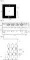
- a recess part 214amay be formed on one surface of the second substrate 214.
- the recess part 214amay have a concave structure.
- the actuator 260 for transferring the vibrationmay be positioned in the recess part 214a. That is, the recess part 214a may receive the actuator 260 therein.
- one of the first and second electrode units 252 and 254may be positioned in the recess part 214a. For instance, referring to FIG. 5 , the first electrode unit 252 may be positioned in the recess part 214a.
- the recess part 214awhen viewed from the front, may have a rectangular shape, but the embodiment is not limited thereto.
- the recess part 214awhen viewed from the front, may have various shapes, such as a circular shape, a triangular shape or a hexagonal shape. That is, the shape of the recess part 214a may vary depending on the performance of the actuator 260 positioned in the recess part 214a.
- a depth D of the recess part 214amay correspond to the sum of the thickness of the first electrode unit 252 and the thickness of the actuator 260. This is because the first electrode unit 252 and the actuator 260 may be positioned in the recess part 214a.
- the recess part 214amay have a depth D in the range of 1nm to 200 ⁇ m.
- the depth D of the recess part 214amay vary depending on the thickness of the actuator 260 positioned in the recess part 214a.
- the recess part 214amay have a width W in the range of 100 ⁇ m to 1mm.
- a recognition cell in the finger of the personhas a very small resolution of about 1mm.
- the recess part 214amust have a small size and many arrays corresponding to the tactile sense.
- a plurality of recess parts 214aare provided while extending in first and second directions.
- the electrode units 252 and 254may include a first electrode unit 252 and a second electrode unit 254.
- the first electrode unit 252may extend in the first direction and the second electrode unit 254 may extend in the second direction.
- the first electrode unit 252may be a positive (+) electrode and the second electrode unit 254 may be a negative (-) electrode.
- the first and second electrode units 252 and 254may cause vibration to the actuator 260 at the input position.
- the haptic unit 200receives information about the detected input position from the input unit 100 and generates the vibration through the first and second electrode units 252 and 254 at the input position.
- At least one of the first and second electrode units 252 and 254may have a thickness in the range of 1nm to 100nm.
- the thickness of the first and second electrode units 252 and 254may vary depending on the thickness of the actuator 260.
- At least one of the first and second electrode units 252 and 254may include at least one selected from the group consisting of indium tin oxide (ITO), carbon nano tube, Ag nano wire, graphene, and conductive polymer.
- ITOindium tin oxide
- carbon nano tubecarbon nano tube
- Ag nano wireAg nano wire
- graphenegraphene
- conductive polymerconductive polymer
- the actuator 260is positioned in the recess part 214a. Since the actuator 260 is positioned in the recess part 214a, the thickness of the touch panel may be prevented from being increased. In addition, the actuator 260 is positioned inside the second substrate 214, so that the actuator 260 is protected and prevented from being damaged.
- the haptic feedbackis possible only at an input part of the touch panel rather than generated by vibrating the body of the touch panel using the actuator 260.
- the actuator 260may generate vibration and transfer the vibration to the touch panel. That is, the tactile sense may be impressed to the touch panel by the actuator 260.
- the actuator 260is provided in the active area AA, which is the input part of the touch panel, the accuracy and sensitivity of the touch input can be improved.
- the actuator 260is transparent. That is, since the actuator 260 is positioned in the active area AA, the actuator 260 is transparent, so the degradation of visibility of the touch panel can be prevented.
- the actuator 260may include at least one of hydrogel, nafion, electroactive polymer, a piezoelectric actuator, and an MEMS (micro electro mechanical systems) actuator.
- the protective unit 270may be formed on the second substrate 241.
- the protective unit 270may be positioned on the second electrode unit 254. That is, the protective unit 270 may be aligned at the outermost portion of the haptic unit 200.
- the protective unit 270may have the moisture reservation function. In addition, the protective unit 270 may protect the haptic unit 200 from external impact.
- the protective unit 270may have transmissivity of 90% or above. Thus, transmissivity of the touch panel may not be lowered.
- the protective unit 270may have a thickness in the range of 1nm to 100 nm. The thickness of the protective unit 270 may vary depending on the thickness of the actuator 260.
- the protective unit 270may include a transparent polymer film.
- the protective unit 270may include at least one of polydimethylsiloxane (PDMS), polyimide (PI), polyvinylidene fluoride (PVDF), silicon gel and polyester.
- PDMSpolydimethylsiloxane
- PIpolyimide
- PVDFpolyvinylidene fluoride
- the second substrate 214 including the recess part 214ais prepared.
- the recess part 214amay be formed by etching the second substrate 214.
- the recess part 214amay be formed through deep reactive-ion etching (DRIE) using plasma including one of SF6 and O2.
- DRIEdeep reactive-ion etching
- the embodimentis not limited thereto, and the recess part 214a may be formed through laser etching or photo glass etching using a photo mask.
- a chamfering processis performed and then a reinforcing process is performed. For instance, one of chemical reinforcing, thermal reinforcing and coating reinforcing processes may be performed.
- the first electrode unit 252may be formed in the first direction of the second substrate 214.
- the first electrode unit 252may be formed by patterning a transparent electrode material.
- the patterning processmay include one of photolithography, physical vapor deposition (PVD), chemical vapor deposition (CVD), printing and coating.
- the actuator 260may be formed in the recess part 214a. Similar to the first electrode unit 252, the actuator 260 may be formed through the patterning process. For instance, if the actuator 260 includes hydrogel, the hydrogel may be formed by coating monomer on the second substrate 214 and then polymerizing the monomer through the lithography process. Then, the washing process is performed such that unexposed parts are washed and exposed parts remain, so that the actuator 260 can be patterned. That is, the actuator 260 may be formed only in the recess part 214a.
- the second electrode unit 254may be formed in the second direction of the second substrate 214. Similar to the first electrode unit 252, the second electrode unit 254 may be formed by patterning a transparent electrode material.
- the protective unit 270may be formed on the entire surface of the second electrode part 254 to protect the haptic part 200.
- the protective unit 270may be formed by coating a thin and transparent film having the moisture reservation function.
- a touch panel according to the second embodimentwill be described with reference to FIG. 9 .
- the description about the elements identical to or similar to those of the first embodimentwill be omitted.
- FIG. 9is a sectional view showing the touch panel according to the second embodiment.
- the touch panel according to the second embodimenthas no the first substrate 112 (see, FIG. 2 ) provided in the touch panel according to the first embodiment. That is, the input unit and the haptic unit are provided on the same substrate.
- the substrateincludes a first surface and a second surface opposite to each other, the input unit is provided on the first surface, the haptic unit is provided on the second surface.
- the transparent electrode 130, the wiring 140, the recess part 214a, the actuator 260 and the electrode units 252 and 254are formed on the second substrate 214, so the thickness of the touch panel may be reduced.
- FIG. 10is a sectional view showing the touch panel according to the third embodiment.
- the touch panel according to the third embodimenthas a structure in which the haptic unit 200 is turned over as compared with the haptic unit 200 of the touch panel according to the first embodiment.
- the recess part 214ais formed on the bottom surface of the second substrate 214 so that the actuator 260 positioned in the recess part 214a may be more stably protected from the external impact and contamination.
- FIG. 11is a schematic sectional view showing the LCD according to the embodiment.
- the LCD according to the present embodimentmay include a liquid crystal panel in which the touch panel according to the first embodiment is mounted.
- the touch panel according to the first embodimentmay be laminated on the surface of the liquid crystal panel 300 such that information can be input from the outside through a screen of the liquid crystal panel 300. That is, the touch panel may be bonded to the liquid crystal panel 300 by an adhesive 90.
- the adhesive 90may include an optical transparent adhesive.
- the liquid crystal panel 300is a display unit of the LCD and displays images by adjusting light transmissivity of liquid crystal cells injected between two glass substrates. Each of the liquid crystal cells adjusts the quantity of light passing therethrough in response to a video signal, that is, a corresponding pixel signal.
- the liquid crystal panel 300may include a liquid crystal material 328 injected between a lower glass substrate 324a and an upper glass substrate 324b and a ball spacer 326.
- a gate line, an insulating layer, a pixel electrode and a first alignment layermay be sequentially formed on the lower glass substrate 324a.
- a black matrix, a color filter, a common electrode, and a second alignment layermay be sequentially formed on the bottom surface of the upper glass substrate 324b.
- the upper and lower glass substrates 324a and 324bare spaced apart from each other by the ball spacer 326. In detail, the interval between the upper and lower glass substrates 324a and 324b can be uniformly maintained by the ball spacer 326, so that the liquid crystal material 328 has a uniform thickness.
- the haptic unit 200 generating the hapticis positioned on the liquid crystal panel 300, so the liquid crystal panel 300 can be prevented from being damaged.
- the haptic unit 200is positioned closer to a touch surface of the touch panel, so sensitivity can be more improved and the user's experience can be maximized.
- FIG. 11shows the LCD including the liquid crystal panel 300 combined with the touch panel according to the first embodiment
- the embodimentis not limited thereto.
- the LCDmay include the liquid crystal panel 300 combined with the touch panel according to the second embodiment or third embodiment.
- any reference in this specification to "one embodiment,” “an embodiment,” “example embodiment,” etc.means that a particular feature, structure, or characteristic described in connection with the embodiment is included in at least one embodiment of the invention.
- the appearances of such phrases in various places in the specificationare not necessarily all referring to the same embodiment.
Landscapes
- Engineering & Computer Science (AREA)
- Physics & Mathematics (AREA)
- General Engineering & Computer Science (AREA)
- Theoretical Computer Science (AREA)
- General Physics & Mathematics (AREA)
- Human Computer Interaction (AREA)
- Nonlinear Science (AREA)
- Crystallography & Structural Chemistry (AREA)
- Chemical & Material Sciences (AREA)
- Mathematical Physics (AREA)
- Optics & Photonics (AREA)
- Quality & Reliability (AREA)
- Position Input By Displaying (AREA)
- User Interface Of Digital Computer (AREA)
Description
- The disclosure relates to a touch panel and a liquid crystal display including the same.
- In general, a touch panel is a device to input information into a computer and is used together with various display devices including a cathode ray tube and a liquid crystal display (LCD). When installed in the LCD, the touch panel allows a user to select icons or items displayed on the LCD by touching a predetermined region of the touch panel corresponding to the icons or items
- Recently, as the multimedia technology and the display technology have made rapid progress, the resolution of the LCD of a portable communication device has been improved, so the touch panel is increasingly used in the portable communication device.
- The touch panel may be mainly classified into a resistive touch panel and a capacitive touch panel. In the resistive touch panel, glass is shorted with an electrode due to the pressure of an input device so that a touch point is detected. In the capacitive touch panel, the variation in capacitance between electrodes is detected when a finger of the user touches the capacitive touch panel, so that the touch point is detected.
- However, users of the portable communication device do not satisfy with the use of a transparent touch window, but demand for interfaces, which can be used more naturally, readily and beneficially.
- In this regard, a haptic function is provided in the portable communication device.
JP2011002926 - The haptic refers to the tactile sense imparted to a person when the person touches an object using a tip of a finger or a stylus pen and includes the tactile feedback, which is felt when a skin touches a surface of the object, and the kinesthetic force feedback, which is felt when the movement of the articulations and muscles is interrupted.
- As an example of a device for providing the haptic function, there is provided a device having an actuator installed at a lower portion of the touch panel. If the actuator is driven, the driving force of the actuator is transferred to the touch panel fixedly connected to the actuator, so the user can recognize the driving force of the actuator.
- However, an additional space is necessary in order to install the actuator for providing the haptic function in the conventional portable communication device using the touch panel. Since a spacer must be inserted between a touch electrode unit and the LCD to provide the space, the thickness of the conventional portable communication device may be increased, causing a problem in terms of slimness and miniaturization.
- In addition, the actuator according to the related art requires a predetermined space and a predetermined size for driving. Thus, if the actuator is mounted together with the touch electrode pat and the LCD, a predetermined mounting space is necessary, so the visibility of the LCD may be degraded.
- Therefore, an apparatus capable of mounting an actuator providing a superior touch sense to a touch panel of a potable communication device without an additional mounting space is necessary.
- An object of the disclosure is to provide a touch panel including an actuator while minimizing an increase of a thickness and improving a touch sense.
- According to one embodiment of the disclosure, there is provided a touch panel according to claim 1.
- According to another embodiment of the disclosure, there is provided a liquid crystal display according to claim 15.
- The touch panel according to the embodiments includes an input unit for inputting information and a haptic unit for applying vibration. An actuator included in the haptic unit is disposed in a recess part of a substrate. Since the haptic unit is disposed in the recess part of the substrate, the thickness of the touch panel may not be increased. In addition, the actuator is disposed inside a second substrate, so that the actuator can be protected and prevented from being damaged.
- Further, the haptic feedback is possible only at an input part of the touch panel rather than generated by vibrating the body of the touch panel using the actuator
- The actuator may generate vibration and transfer the vibration to the touch panel. That is, the tactile sense may be impressed to the touch panel by the actuator. In addition, since the actuator is provided in an active area, which is the input part of the touch panel, the accuracy and sensitivity of the touch input can be improved.
- Further, the actuator is transparent, so the degradation of visibility of the touch panel can be prevented.
- Meanwhile, according to an LCD of the embodiments, the haptic unit for generating the haptic is disposed on a liquid crystal panel, so the liquid crystal panel can be prevented from being damaged. Further, the haptic unit is positioned closer to a touch surface of the touch panel, so sensitivity can be more improved and the user's experience can be maximized.
FIG. 1 is a schematic plan view showing a touch panel according to the first embodiment;FIG. 2 is a sectional view taken along line A-A' ofFIG. 1 ;FIG. 3 is an enlarged plan view of a 'B' portion of an input unit included in a touch panel according to the first embodiment shown inFIG. 1 ;FIGS. 4 to 8 are plan views for explaining the manufacturing process of a haptic unit included in a touch panel according to the first embodiment;FIG. 9 is a sectional view showing a touch panel according to the second embodiment;FIG. 10 is a sectional view showing a touch panel according to the third embodiment; andFIG. 11 is a schematic sectional view showing an LCD according to the embodiment.- In the description of the embodiments, it will be understood that when each layer (film), region, patter or structure is referred to as being "on" or "under" another layer (film), region, patter or structure, it can be "directly" or "indirectly" on the other layer (film), region, patter or structure or one or more intervening layers may also be present. Such a position has been described with reference to the drawings.
- The thickness and size of each layer (film), region, patter or structure shown in the drawings may be modified for the purpose of convenience or clarity. In addition, the size of the elements does not utterly reflect an actual size.
- Hereinafter, embodiments will be described in detail with reference to accompanying drawings.
- First, a touch panel according to the first embodiment will be described in detail with reference to
FIGS. 1 to 8 FIG. 1 is a schematic plan view showing the touch panel according to the first embodiment,FIG. 2 is a sectional view taken along line A-A' ofFIG. 1, FIG. 3 is an enlarged plan view of a 'B' portion of an input unit included in the touch panel according to the first embodiment shown inFIG. 1 , andFIGS. 4 to 8 are plan views for explaining the manufacturing process of a haptic unit included in the touch panel according to the first embodiment.- Referring to
FIGS. 1 to 8 , the touch panel according to the first embodiment (background art) includes an active area AA for detecting apposition of an input device and a dummy area DA disposed around the active area AA. - A
transparent electrode 130 for detecting the input device may be formed on the active area AA. In addition, awiring 140 connected to thetransparent electrode 130 and a printed circuit board connecting thewiring 140 to an external circuit (not shown) may be formed on the dummy area DA. Anouter dummy layer 120 may be formed on the dummy area DA and a logo 120a may be formed on theouter dummy layer 120. Hereinafter, the touch panel having the above structure will be described in more detail. - Referring to
FIG. 2 , the touch panel according to the first embodiment includes aninput unit 100 and ahaptic unit 200. - The
input unit 100 may be divided into several sections in such a manner that a section to which pressure is applied by pressure elements or scanning is detected and position information of the section is sent to a computer. - The
input unit 100 may include afirst substrate 112, atransparent electrode 130 and awiring 140. Theouter dummy layer 120 and thetransparent electrode 130 are formed onfirst substrate 112. In addition, thewiring 140 is connected to thetransparent electrode 130 and a printed circuit board (not shown) is connected to thewiring 140. - The
first substrate 112 may be formed by using various materials capable of supporting theouter dummy layer 120, thetransparent electrode 130 and thewiring 140 formed on thefirst substrate 112. For instance, thefirst substrate 112 may include a glass substrate or a plastic substrate. - The
outer dummy layer 120 is formed on the dummy area DA formed at a bottom surface of thefirst substrate 112. Theouter dummy layer 120 may be coated with a material having a predetermined color such that thewiring 140 and the printed circuit board may not be seen from the outside. Theouter dummy layer 120 may have a predetermined color suitable for the external appearance of theouter dummy layer 120. For instance, theouter dummy layer 120 may include a black pigment to represent a black color. In addition, the log 120a (see,FIG. 1 ) can be formed on theouter dummy layer 120 in various schemes. Theouter dummy layer 120 may be formed through the deposition, printing, or wet coating scheme. - The
transparent electrode 130 is formed on the bottom surface of the first substrate 112.112. Thetransparent electrode 130 may have various shapes suitable for detecting the touch of the input device, such as a finger. - For instance, as shown in
FIG. 3 , thetransparent electrode 130 may include a firsttransparent electrode 132 and a secondtransparent electrode 134. The first and secondtransparent electrodes sensor units connection units sensor units connection unit 132b of the firsttransparent electrode 132 connects thesensor unit 132a in the first direction (transverse direction in the drawing) and theconnection unit 134b of the secondtransparent electrode 134 connects thesensor unit 134a in the second direction (longitudinal direction in the drawing). - An insulating
layer 136 is disposed at the intersection between theconnection unit 132b of the firsttransparent electrode 132 and theconnection unit 134b of the secondtransparent electrode 134 to prevent the electric short between the first and secondtransparent electrodes layer 136 may be formed by using a transparent insulating material capable of insulating theconnection units layer 136 may include metal oxide, such as silicon oxide, polymer or acryl resin. - According to the embodiment, for instance, the
sensor units transparent electrodes - In this manner, if the input device, such as the finger, touches the touch panel, capacitance difference may occur at the portion touched by the input device, so the portion having the capacitance difference may be determined as the contact position. According to the embodiment, the
transparent electrode 130 is applied to the capacitive touch panel, but the embodiment is not limited thereto. For instance, thetransparent electrode 130 may be applied to the resistive touch panel. - The
transparent electrode 130 may include a transparent conductive material such that electricity may flow without interfering with transmission of light. In this regard, thetransparent electrode 130 may include various materials, such as metal oxide including indium tin oxide, indium zinc oxide, copper oxide, tin oxide, zinc oxide or titanium oxide, a carbon nanotube (CNT), or a conductive polymer material. - The
transparent electrode 130 may be formed through various thin film deposition technologies, such as physical vapor deposition (PVD) or chemical vapor deposition (CVD). For instance, thetransparent electrode 130 may be formed through reactive sputtering, which is one of the physical vapor depositions. At this time, if thetransparent electrode 130 is formed by using the indium tin oxide, the content of tin may be equal to or less than 10%. Thus, light transmissivity can be improved. Then, the indium tin oxide is crystallized through the annealing process, so that electric conductivity can be improved. However, the embodiment is not limited to the above, and thetransparent electrode 130 may be formed through various methods. - In addition, the
transparent electrode 130 may be formed through a printing process. The printing process can be performed by adopting various printing schemes, such as gravure off set, reverse off set, screen printing or gravure printing. In particular, if thetransparent electrode 130 is formed through the printing process, a printable paste material can be employed. For instance, thetransparent electrode 130 may be formed by using carbon nano tube (CNT), conductive polymer or Ag nano wire ink. - If the
transparent electrode 130 is formed through the printing process, the manufacturing process can be simplified and the manufacturing cost can be reduced. - The
wiring 140 connected to thetransparent electrode 130 and the printed circuit board (not shown) connected to thewiring 140 are provided on the dummy area DA. Since thewiring 140 is formed on the dummy area DA, thewiring 140 may be formed by using a metal having superior electric conductivity. Various types of printed circuit boards may be used as the printed circuit board. For instance, a flexible printed circuit board(FPCB) may be used as the printed circuit board. - Although not shown in the drawing, an anti-scattering film can be formed to cover the
transparent electrode 130 and thewiring 140. The anti-scattering film can be formed by using various materials with various structures to prevent particles, which are generated when the touch panel is broken by external impact, from being scattered. - Then, referring again to
FIG. 2 , thehaptic unit 200 may be aligned on theinput unit 100. Thehaptic unit 200 may apply vibration to the touch panel. In detail, when the touch panel is touched, thehaptic unit 200 generates the vibration to make the feedback by stimulating the tactile sense to the tip of the finger or the stylus pen. - The
haptic unit 200 may include asecond substrate 214,electrode units actuator 260 and aprotective unit 270. - The
second substrate 214 may be formed by using various materials capable of supporting theelectrode units actuator 260 and theprotective unit 270 formed on thesecond substrate 214. For instance, thesecond substrate 214 may be formed by using glass or a film. - The
second substrate 214 may have transmissivity of 90% or above. Thus, the transmissivity of the touch panel may not be degraded. - A
recess part 214a may be formed on one surface of thesecond substrate 214. Therecess part 214a may have a concave structure. Theactuator 260 for transferring the vibration may be positioned in therecess part 214a. That is, therecess part 214a may receive theactuator 260 therein. In addition, one of the first andsecond electrode units recess part 214a. For instance, referring toFIG. 5 , thefirst electrode unit 252 may be positioned in therecess part 214a. - Referring to
FIG. 4 , when viewed from the front, therecess part 214a may have a rectangular shape, but the embodiment is not limited thereto. For instance, when viewed from the front, therecess part 214a may have various shapes, such as a circular shape, a triangular shape or a hexagonal shape. That is, the shape of therecess part 214a may vary depending on the performance of theactuator 260 positioned in therecess part 214a. - Referring to
FIG. 4 , a depth D of therecess part 214a may correspond to the sum of the thickness of thefirst electrode unit 252 and the thickness of theactuator 260. This is because thefirst electrode unit 252 and theactuator 260 may be positioned in therecess part 214a. - In detail, the
recess part 214a may have a depth D in the range of 1nm to 200µm. The depth D of therecess part 214a may vary depending on the thickness of theactuator 260 positioned in therecess part 214a. - The
recess part 214a may have a width W in the range of 100µm to 1mm. A recognition cell in the finger of the person has a very small resolution of about 1mm. Thus, therecess part 214a must have a small size and many arrays corresponding to the tactile sense. - Thus, a plurality of
recess parts 214a are provided while extending in first and second directions. - The
electrode units first electrode unit 252 and asecond electrode unit 254. Thefirst electrode unit 252 may extend in the first direction and thesecond electrode unit 254 may extend in the second direction. - The
first electrode unit 252 may be a positive (+) electrode and thesecond electrode unit 254 may be a negative (-) electrode. - The first and
second electrode units actuator 260 at the input position. - That is, the
haptic unit 200 receives information about the detected input position from theinput unit 100 and generates the vibration through the first andsecond electrode units - At least one of the first and
second electrode units second electrode units actuator 260. - At least one of the first and
second electrode units - The
actuator 260 is positioned in therecess part 214a. Since theactuator 260 is positioned in therecess part 214a, the thickness of the touch panel may be prevented from being increased. In addition, theactuator 260 is positioned inside thesecond substrate 214, so that theactuator 260 is protected and prevented from being damaged. - Further, the haptic feedback is possible only at an input part of the touch panel rather than generated by vibrating the body of the touch panel using the
actuator 260. - The
actuator 260 may generate vibration and transfer the vibration to the touch panel. That is, the tactile sense may be impressed to the touch panel by theactuator 260. In addition, since theactuator 260 is provided in the active area AA, which is the input part of the touch panel, the accuracy and sensitivity of the touch input can be improved. - Further, the
actuator 260 is transparent. That is, since theactuator 260 is positioned in the active area AA, theactuator 260 is transparent, so the degradation of visibility of the touch panel can be prevented. - The
actuator 260 may include at least one of hydrogel, nafion, electroactive polymer, a piezoelectric actuator, and an MEMS (micro electro mechanical systems) actuator. - The
protective unit 270 may be formed on the second substrate 241. In detail, theprotective unit 270 may be positioned on thesecond electrode unit 254. That is, theprotective unit 270 may be aligned at the outermost portion of thehaptic unit 200. - The
protective unit 270 may have the moisture reservation function. In addition, theprotective unit 270 may protect thehaptic unit 200 from external impact. - The
protective unit 270 may have transmissivity of 90% or above. Thus, transmissivity of the touch panel may not be lowered. - The
protective unit 270 may have a thickness in the range of 1nm to 100 nm. The thickness of theprotective unit 270 may vary depending on the thickness of theactuator 260. - The
protective unit 270 may include a transparent polymer film. In detail, theprotective unit 270 may include at least one of polydimethylsiloxane (PDMS), polyimide (PI), polyvinylidene fluoride (PVDF), silicon gel and polyester. - Hereinafter, the manufacturing process for the
haptic unit 200 included in the touch panel according to the embodiment will be described with reference toFIGS. 4 to 8 . - First, referring to
FIG. 4 , thesecond substrate 214 including therecess part 214a is prepared. Therecess part 214a may be formed by etching thesecond substrate 214. For instance, therecess part 214a may be formed through deep reactive-ion etching (DRIE) using plasma including one of SF6 and O2. However, the embodiment is not limited thereto, and therecess part 214a may be formed through laser etching or photo glass etching using a photo mask. After the etching process, a chamfering process is performed and then a reinforcing process is performed. For instance, one of chemical reinforcing, thermal reinforcing and coating reinforcing processes may be performed. - Then, referring to
FIG. 5 , thefirst electrode unit 252 may be formed in the first direction of thesecond substrate 214. Thefirst electrode unit 252 may be formed by patterning a transparent electrode material. The patterning process may include one of photolithography, physical vapor deposition (PVD), chemical vapor deposition (CVD), printing and coating. - After that, referring to
FIG. 6 , theactuator 260 may be formed in therecess part 214a. Similar to thefirst electrode unit 252, theactuator 260 may be formed through the patterning process. For instance, if theactuator 260 includes hydrogel, the hydrogel may be formed by coating monomer on thesecond substrate 214 and then polymerizing the monomer through the lithography process. Then, the washing process is performed such that unexposed parts are washed and exposed parts remain, so that theactuator 260 can be patterned. That is, theactuator 260 may be formed only in therecess part 214a. - Then, referring to
FIG. 7 , thesecond electrode unit 254 may be formed in the second direction of thesecond substrate 214. Similar to thefirst electrode unit 252, thesecond electrode unit 254 may be formed by patterning a transparent electrode material. - After that, referring to
FIG. 8 , theprotective unit 270 may be formed on the entire surface of thesecond electrode part 254 to protect thehaptic part 200. Theprotective unit 270 may be formed by coating a thin and transparent film having the moisture reservation function. - Hereinafter, a touch panel according to the second embodiment will be described with reference to
FIG. 9 . For the purpose of simplicity and clarity, the description about the elements identical to or similar to those of the first embodiment will be omitted. FIG. 9 is a sectional view showing the touch panel according to the second embodiment.- Referring to
FIG. 9 , the touch panel according to the second embodiment has no the first substrate 112 (see,FIG. 2 ) provided in the touch panel according to the first embodiment. That is, the input unit and the haptic unit are provided on the same substrate. In detail, the substrate includes a first surface and a second surface opposite to each other, the input unit is provided on the first surface, the haptic unit is provided on the second surface. According to thetransparent electrode 130, thewiring 140, therecess part 214a, theactuator 260 and theelectrode units second substrate 214, so the thickness of the touch panel may be reduced. - Hereinafter, a touch panel according to the third embodiment will be described with reference to
FIG. 10 . FIG. 10 is a sectional view showing the touch panel according to the third embodiment.- Referring to
FIG. 10 , the touch panel according to the third embodiment has a structure in which thehaptic unit 200 is turned over as compared with thehaptic unit 200 of the touch panel according to the first embodiment. In detail, therecess part 214a is formed on the bottom surface of thesecond substrate 214 so that theactuator 260 positioned in therecess part 214a may be more stably protected from the external impact and contamination. - Hereinafter, a liquid crystal display (LCD) according to the embodiment will be described with reference to
FIG. 11. FIG. 11 is a schematic sectional view showing the LCD according to the embodiment. - The LCD according to the present embodiment may include a liquid crystal panel in which the touch panel according to the first embodiment is mounted. The touch panel according to the first embodiment may be laminated on the surface of the
liquid crystal panel 300 such that information can be input from the outside through a screen of theliquid crystal panel 300. That is, the touch panel may be bonded to theliquid crystal panel 300 by an adhesive 90. For instance, the adhesive 90 may include an optical transparent adhesive. - The
liquid crystal panel 300 is a display unit of the LCD and displays images by adjusting light transmissivity of liquid crystal cells injected between two glass substrates. Each of the liquid crystal cells adjusts the quantity of light passing therethrough in response to a video signal, that is, a corresponding pixel signal. - The
liquid crystal panel 300 may include aliquid crystal material 328 injected between alower glass substrate 324a and anupper glass substrate 324b and aball spacer 326. In detail, although not shown in the drawing, a gate line, an insulating layer, a pixel electrode and a first alignment layer may be sequentially formed on thelower glass substrate 324a. A black matrix, a color filter, a common electrode, and a second alignment layer may be sequentially formed on the bottom surface of theupper glass substrate 324b. The upper andlower glass substrates ball spacer 326. In detail, the interval between the upper andlower glass substrates ball spacer 326, so that theliquid crystal material 328 has a uniform thickness. - According to the LCD of the present embodiment, the
haptic unit 200 generating the haptic is positioned on theliquid crystal panel 300, so theliquid crystal panel 300 can be prevented from being damaged. In addition, thehaptic unit 200 is positioned closer to a touch surface of the touch panel, so sensitivity can be more improved and the user's experience can be maximized. - Although
FIG. 11 shows the LCD including theliquid crystal panel 300 combined with the touch panel according to the first embodiment, the embodiment is not limited thereto. According to another embodiment, the LCD may include theliquid crystal panel 300 combined with the touch panel according to the second embodiment or third embodiment. - Any reference in this specification to "one embodiment," "an embodiment," "example embodiment," etc., means that a particular feature, structure, or characteristic described in connection with the embodiment is included in at least one embodiment of the invention. The appearances of such phrases in various places in the specification are not necessarily all referring to the same embodiment. Further, when a particular feature, structure, or characteristic is described in connection with any embodiment, it is submitted that it is within the purview of one skilled in the art to effects such feature, structure, or characteristic in connection with other ones of the embodiments.
- Although a preferred embodiment of the disclosure has been described for illustrative purposes, those skilled in the art will appreciate that various modifications, additions and substitutions are possible, without departing from the scope of the invention as disclosed in the accompanying claims.
Claims (15)
- A touch panel comprising an active area (AA) for detecting position of an input and a dummy area (DA) disposed around the active area, the touch panel further comprising:an input unit (100) for inputting information; anda haptic unit (200) positioned on the input unit (100),wherein said haptic device (200) is to apply vibration;wherein the input unit (100) comprises:a sensor unit (130) for detecting an input position on the first surface ; anda wiring (140) electrically connected to the sensor unit andwherein the haptic unit (200) comprises:an electrode unit (252,254) aligned on the second surface to receive position information;characterized in that said input unit (100) and said haptic unit (200) being provided on a respective first and second surfaces, opposite to each other, of a same substrate (214);in that the haptic device (200) comprises a recess part (214a) on said second surface (214) and an actuator (260) aligned on the recess part (214a) to transfer vibration force, said actuator (260) being transparent; andin that the substrate (214) comprises a first thickness and a second thickness in the active area (AA), the first thickness corresponding to a thickness of the substrate in the dummy area (DA) and the second thickness corresponding to a thickness excluding a depth (D) of the recess part (214a) from the first thickness, the first thickness being greater than the second thickness, andin that the recess part (214a) has a concave structure such that the actuator is disposed in the concave structure of the active area (AA).
- The touch panel of claim 1, wherein the electrode unit includes a first electrode unit (252) extending in a first direction and a second electrode unit (254) extending in a second direction.
- The touch panel of claim 2, wherein the first electrode unit (252), the actuator (260) and the second electrode unit (254) are sequentially aligned on the substrate (214).
- The touch panel of any one of claims 2 to 3, wherein the actuator (260) is interposed between the first electrode unit (252) and the second electrode unit (254).
- The touch panel of any one of claims 2 to 4, wherein a sum of a thickness of the first electrode unit (252) and a thickness of the actuator (260) corresponds to a depth of the recess part (214a).
- The touch panel of any one of claims 2 to 5, wherein the recess part (214a) has the depth in a range of 1nm to 200µm.
- The touch panel of any one of claims 2 to 6, wherein a plurality of recess parts (214a) are aligned while extending in first and second directions.
- The touch panel of any one of claims 2 to 7, wherein the recess part (214a) has a width in a range of 100µm to 1mm.
- The touch panel of any one of claims 2 to 8, wherein at least one of the first and second electrode units has a thickness in a range of 1 nm to 100nm.
- The touch panel of any one of claims 1 to 9, wherein the actuator (260) includes at least one selected from the group consisting of hydrogel, nafion, electroactive polymer, a piezoelectric actuator, and an MEMS (micro electro mechanical systems) actuator.
- The touch panel of any one of claims 2 to 10, wherein at least one of the first and second electrode units includes at least one selected from the group consisting of indium tin oxide (ITO), carbon nano tube, Ag nano wire, graphene, and conductive polymer.
- The touch panel of any one of claims 1 to 11, wherein the substrate (214) includes a glass or a film.
- The touch panel of any one of claims 2 to 12, further comprising a protective unit (270) on the substrate (214).
- The touch panel of claim 13, wherein the protective unit (270) is aligned on the second electrode unit (254).
- A liquid crystal display comprising:a liquid crystal panel (300) for displaying images; anda touch panel according to claim 1, aligned at a display side of the liquid crystal panel such that information is input thereto from an outside,wherein the touch panel comprises an active area (AA) for detecting position of an input and a dummy area (DA) disposed around the active area, the touch panel further comprises:an input unit (100) for inputting the information; anda haptic unit (200),wherein said haptic device (200) is to apply vibration;wherein the input unit (100) comprises:a sensor unit (130) for detecting an input position on the first surface ; anda wiring (140) electrically connected to the sensor unit, andwherein the haptic unit (200) comprises:an electrode unit (252,254) aligned on the second surface to receive position information;characterized in that said input unit (100) and said haptic unit (200) being provided on a respective first and second surfaces, opposite to each other, of a same substrate (214); andin that the haptic device (200) comprises a recess part (214a) on said second surface and an actuator (260) aligned on the recess part (214a) to transfer vibration force, said actuator (260) being transparent;in that the substrate (214) comprises a first thickness and a second thickness in the active area (AA), the first thickness corresponding to a thickness of the substrate in the dummy area (DA) and the second thickness corresponding to a thickness excluding a depth (D) of the recess part (214a) from the first thickness, the first thickness being greater than the second thickness,andin that the recess part (214a) has a concave structure such that the actuator is disposed in the concave structure of the active area (AA).
Applications Claiming Priority (2)
| Application Number | Priority Date | Filing Date | Title |
|---|---|---|---|
| KR1020110088540AKR101826709B1 (en) | 2011-09-01 | 2011-09-01 | Touch panel and liquid crystla display comprising the same |
| PCT/KR2012/007027WO2013032302A2 (en) | 2011-09-01 | 2012-08-31 | Touch panel and liquid crystal display comprising the same |
Publications (3)
| Publication Number | Publication Date |
|---|---|
| EP2751649A2 EP2751649A2 (en) | 2014-07-09 |
| EP2751649A4 EP2751649A4 (en) | 2015-06-03 |
| EP2751649B1true EP2751649B1 (en) | 2021-01-20 |
Family
ID=47757089
Family Applications (1)
| Application Number | Title | Priority Date | Filing Date |
|---|---|---|---|
| EP12828030.2AActiveEP2751649B1 (en) | 2011-09-01 | 2012-08-31 | Touch panel and liquid crystal display comprising the same |
Country Status (5)
| Country | Link |
|---|---|
| US (1) | US9639188B2 (en) |
| EP (1) | EP2751649B1 (en) |
| KR (1) | KR101826709B1 (en) |
| CN (1) | CN103907083B (en) |
| WO (1) | WO2013032302A2 (en) |
Families Citing this family (22)
| Publication number | Priority date | Publication date | Assignee | Title |
|---|---|---|---|---|
| WO2015041268A1 (en)* | 2013-09-20 | 2015-03-26 | 株式会社村田製作所 | Detection sensor and input device |
| KR102199333B1 (en)* | 2014-07-07 | 2021-01-06 | 엘지이노텍 주식회사 | Touch window |
| EP2985680B1 (en)* | 2014-08-14 | 2017-05-17 | LG Electronics Inc. | Conductive film, touch panel including the conductive film and display apparatus including the conductive film |
| KR102209305B1 (en)* | 2014-08-14 | 2021-01-29 | 엘지전자 주식회사 | Conductive film, and touch panel and display apparatus including the conductive film |
| EP3035158B1 (en)* | 2014-12-18 | 2020-04-15 | LG Display Co., Ltd. | Touch sensitive device and display device comprising the same |
| TWI574190B (en)* | 2014-12-18 | 2017-03-11 | Lg顯示器股份有限公司 | Touch sensitive device and display device comprising the same |
| CN107037899A (en)* | 2015-07-16 | 2017-08-11 | 鸿富锦精密工业(深圳)有限公司 | The touch module of touch-control film and application touch control film |
| KR102368462B1 (en)* | 2015-08-07 | 2022-03-02 | 삼성디스플레이 주식회사 | Fabrication method of glass, fabrication method of display device |
| KR20180041721A (en)* | 2015-08-20 | 2018-04-24 | 로베르트 보쉬 게엠베하 | Layer Arrangement and Input / Output Devices |
| KR101714713B1 (en)* | 2015-09-23 | 2017-03-09 | 숭실대학교산학협력단 | Sensor integrated haptic device and method for manufacturing the same |
| KR102489956B1 (en)* | 2015-12-30 | 2023-01-17 | 엘지디스플레이 주식회사 | Display device and method of driving the same |
| KR102581950B1 (en)* | 2016-08-29 | 2023-09-22 | 삼성디스플레이 주식회사 | Display device and mufacturing method thereof |
| KR102666083B1 (en)* | 2016-10-31 | 2024-05-13 | 엘지디스플레이 주식회사 | Touch sensitive device and display device comprising the same |
| KR102655324B1 (en)* | 2016-12-09 | 2024-04-04 | 엘지디스플레이 주식회사 | Displya device |
| US20180329493A1 (en)* | 2017-05-11 | 2018-11-15 | Immersion Corporation | Microdot Actuators |
| DE102017223638A1 (en) | 2017-12-22 | 2019-06-27 | Robert Bosch Gmbh | MEMS actuator for generating a vibration for a haptic and / or acoustic signaling, data glasses with a MEMS actuator, and method and control device for operating a MEMS actuator |
| DE102017223641A1 (en) | 2017-12-22 | 2019-06-27 | Robert Bosch Gmbh | MEMS actuator for generating a vibration for a haptic and / or acoustic signaling, data glasses with a MEMS actuator, and method and control device for operating a MEMS actuator |
| CN108897450B (en)* | 2018-06-30 | 2021-12-03 | 广州国显科技有限公司 | Touch panel, manufacturing method thereof and display device |
| WO2020010590A1 (en)* | 2018-07-12 | 2020-01-16 | Shenzhen Xpectvision Technology Co., Ltd. | Image sensors with silver-nanoparticle electrodes |
| CN108845710B (en)* | 2018-07-27 | 2021-09-07 | 上海天马微电子有限公司 | Touch panel, driving method thereof and touch device |
| US10802325B2 (en)* | 2018-11-05 | 2020-10-13 | Himax Display, Inc. | Display panel |
| TWI730413B (en)* | 2019-09-17 | 2021-06-11 | 凌巨科技股份有限公司 | Touch module and display device |
Citations (3)
| Publication number | Priority date | Publication date | Assignee | Title |
|---|---|---|---|---|
| US20080309635A1 (en)* | 2007-06-14 | 2008-12-18 | Epson Imaging Devices Corporation | Capacitive input device |
| US20100013745A1 (en)* | 2008-07-21 | 2010-01-21 | Kim Young-Dae | Organic light emitting display device |
| EP2354901A1 (en)* | 2009-06-04 | 2011-08-10 | Inferpoint Systems Limited | Tactile and touch control system |
Family Cites Families (18)
| Publication number | Priority date | Publication date | Assignee | Title |
|---|---|---|---|---|
| JP2001002926A (en) | 1999-06-24 | 2001-01-09 | Toho Chem Ind Co Ltd | Asphalt emulsion composition |
| KR100817639B1 (en)* | 2004-03-19 | 2008-03-27 | 에스에무케이 가부시키가이샤 | Screen-printing metal mask plate and method of resin-sealing vibrating part |
| JP2006215738A (en)* | 2005-02-02 | 2006-08-17 | Sony Corp | Vibration transmitting structure, input device with tactile function and electronic equipment |
| JP4967780B2 (en) | 2007-04-20 | 2012-07-04 | セイコーエプソン株式会社 | Coordinate input device and display device |
| US9823833B2 (en) | 2007-06-05 | 2017-11-21 | Immersion Corporation | Method and apparatus for haptic enabled flexible touch sensitive surface |
| US20090002328A1 (en) | 2007-06-26 | 2009-01-01 | Immersion Corporation, A Delaware Corporation | Method and apparatus for multi-touch tactile touch panel actuator mechanisms |
| US8004501B2 (en) | 2008-01-21 | 2011-08-23 | Sony Computer Entertainment America Llc | Hand-held device with touchscreen and digital tactile pixels |
| GB2462465B (en) | 2008-08-08 | 2013-02-13 | Hiwave Technologies Uk Ltd | Touch sensitive device |
| KR100980463B1 (en)* | 2008-10-21 | 2010-09-07 | 주식회사 삼전 | Touch panel |
| US9746923B2 (en)* | 2009-03-12 | 2017-08-29 | Immersion Corporation | Systems and methods for providing features in a friction display wherein a haptic effect is configured to vary the coefficient of friction |
| KR101067066B1 (en) | 2009-04-03 | 2011-09-22 | 삼성전기주식회사 | Touch screen device |
| KR20100118055A (en) | 2009-04-27 | 2010-11-04 | 최현환 | Tactile sensation type touch panel using polymer |
| JP2011002926A (en) | 2009-06-17 | 2011-01-06 | Hitachi Ltd | Display device with tactile exhibition function |
| KR101622632B1 (en)* | 2009-08-26 | 2016-05-20 | 엘지전자 주식회사 | Mobile terminal |
| KR20110029470A (en) | 2009-09-15 | 2011-03-23 | 엘지전자 주식회사 | Touch panel and portable terminal having same |
| KR101622683B1 (en)* | 2009-12-15 | 2016-05-19 | 엘지전자 주식회사 | Portable terminal |
| CN201583920U (en)* | 2009-12-21 | 2010-09-15 | 瑞声声学科技(深圳)有限公司 | Touch-screen display device |
| KR101710552B1 (en)* | 2010-07-20 | 2017-02-28 | 삼성디스플레이 주식회사 | Touch screen panel |
- 2011
- 2011-09-01KRKR1020110088540Apatent/KR101826709B1/ennot_activeExpired - Fee Related
- 2012
- 2012-08-31WOPCT/KR2012/007027patent/WO2013032302A2/enactiveApplication Filing
- 2012-08-31CNCN201280054088.4Apatent/CN103907083B/ennot_activeExpired - Fee Related
- 2012-08-31USUS14/342,485patent/US9639188B2/ennot_activeExpired - Fee Related
- 2012-08-31EPEP12828030.2Apatent/EP2751649B1/enactiveActive
Patent Citations (3)
| Publication number | Priority date | Publication date | Assignee | Title |
|---|---|---|---|---|
| US20080309635A1 (en)* | 2007-06-14 | 2008-12-18 | Epson Imaging Devices Corporation | Capacitive input device |
| US20100013745A1 (en)* | 2008-07-21 | 2010-01-21 | Kim Young-Dae | Organic light emitting display device |
| EP2354901A1 (en)* | 2009-06-04 | 2011-08-10 | Inferpoint Systems Limited | Tactile and touch control system |
Also Published As
| Publication number | Publication date |
|---|---|
| WO2013032302A3 (en) | 2013-04-25 |
| CN103907083B (en) | 2017-02-22 |
| EP2751649A2 (en) | 2014-07-09 |
| EP2751649A4 (en) | 2015-06-03 |
| US9639188B2 (en) | 2017-05-02 |
| CN103907083A (en) | 2014-07-02 |
| WO2013032302A2 (en) | 2013-03-07 |
| KR101826709B1 (en) | 2018-03-22 |
| KR20130025174A (en) | 2013-03-11 |
| US20160041636A1 (en) | 2016-02-11 |
Similar Documents
| Publication | Publication Date | Title |
|---|---|---|
| EP2751649B1 (en) | Touch panel and liquid crystal display comprising the same | |
| EP2652583B1 (en) | Touch panel, method for manufacturing the same, and liquid crystal display device including the touch panel | |
| CN102687103B (en) | Electro-optic display with touch sensor | |
| US7903091B2 (en) | Touch panel having a speaker function | |
| US7714845B2 (en) | Touch panel and input device including the same | |
| US9831871B2 (en) | Touch panel comprising a piezoelectric material | |
| EP2500805B1 (en) | Touch panel and touch screen having the same | |
| JP2015053055A (en) | Touch window and touch device including the same | |
| US20110128253A1 (en) | Touch screen display device and method of manufacturing the same | |
| WO2010032515A1 (en) | Touch panel, display apparatus, and electronic device | |
| KR20140008440A (en) | Flexible touch screen display | |
| US20120026101A1 (en) | Electric paper associated with touch panel | |
| KR101109312B1 (en) | Touch panel and manufacturing method | |
| US10437362B2 (en) | Touch window and display device comprising same | |
| US20110115725A1 (en) | Touch Panel and Display Device Including the Same and Touch Position Detection Method of Touch Panel | |
| CN103403654A (en) | Input device, electronic apparatus, and portable terminal | |
| KR20130020334A (en) | Touchscreen panel and its manufacturing method | |
| KR101664771B1 (en) | Touch panel and method for driving the same | |
| KR102008736B1 (en) | Touch panel and method for driving the same | |
| KR20150087941A (en) | Electrod members, touch window with the same and display with the same | |
| KR20120135733A (en) | Touch panel, method for manufacturing the same and liquid crystla display comprising touch panel | |
| CN111124171A (en) | Pressure sensor and display device with pressure sensor | |
| KR20200055170A (en) | touch panel for dashboard of vehicle using PEDOT and method of making the same |
Legal Events
| Date | Code | Title | Description |
|---|---|---|---|
| PUAI | Public reference made under article 153(3) epc to a published international application that has entered the european phase | Free format text:ORIGINAL CODE: 0009012 | |
| 17P | Request for examination filed | Effective date:20140303 | |
| AK | Designated contracting states | Kind code of ref document:A2 Designated state(s):AL AT BE BG CH CY CZ DE DK EE ES FI FR GB GR HR HU IE IS IT LI LT LU LV MC MK MT NL NO PL PT RO RS SE SI SK SM TR | |
| DAX | Request for extension of the european patent (deleted) | ||
| A4 | Supplementary search report drawn up and despatched | Effective date:20150507 | |
| RIC1 | Information provided on ipc code assigned before grant | Ipc:G02F 1/1333 20060101ALI20150429BHEP Ipc:G06F 3/041 20060101AFI20150429BHEP | |
| RAP1 | Party data changed (applicant data changed or rights of an application transferred) | Owner name:LG INNOTEK CO., LTD. | |
| STAA | Information on the status of an ep patent application or granted ep patent | Free format text:STATUS: EXAMINATION IS IN PROGRESS | |
| 17Q | First examination report despatched | Effective date:20181008 | |
| GRAP | Despatch of communication of intention to grant a patent | Free format text:ORIGINAL CODE: EPIDOSNIGR1 | |
| STAA | Information on the status of an ep patent application or granted ep patent | Free format text:STATUS: GRANT OF PATENT IS INTENDED | |
| INTG | Intention to grant announced | Effective date:20200826 | |
| GRAS | Grant fee paid | Free format text:ORIGINAL CODE: EPIDOSNIGR3 | |
| GRAA | (expected) grant | Free format text:ORIGINAL CODE: 0009210 | |
| STAA | Information on the status of an ep patent application or granted ep patent | Free format text:STATUS: THE PATENT HAS BEEN GRANTED | |
| AK | Designated contracting states | Kind code of ref document:B1 Designated state(s):AL AT BE BG CH CY CZ DE DK EE ES FI FR GB GR HR HU IE IS IT LI LT LU LV MC MK MT NL NO PL PT RO RS SE SI SK SM TR | |
| REG | Reference to a national code | Ref country code:GB Ref legal event code:FG4D | |
| REG | Reference to a national code | Ref country code:CH Ref legal event code:EP | |
| REG | Reference to a national code | Ref country code:DE Ref legal event code:R096 Ref document number:602012074245 Country of ref document:DE | |
| REG | Reference to a national code | Ref country code:AT Ref legal event code:REF Ref document number:1356979 Country of ref document:AT Kind code of ref document:T Effective date:20210215 | |
| REG | Reference to a national code | Ref country code:IE Ref legal event code:FG4D | |
| REG | Reference to a national code | Ref country code:NL Ref legal event code:MP Effective date:20210120 | |
| REG | Reference to a national code | Ref country code:LT Ref legal event code:MG9D | |
| REG | Reference to a national code | Ref country code:AT Ref legal event code:MK05 Ref document number:1356979 Country of ref document:AT Kind code of ref document:T Effective date:20210120 | |
| PG25 | Lapsed in a contracting state [announced via postgrant information from national office to epo] | Ref country code:PT Free format text:LAPSE BECAUSE OF FAILURE TO SUBMIT A TRANSLATION OF THE DESCRIPTION OR TO PAY THE FEE WITHIN THE PRESCRIBED TIME-LIMIT Effective date:20210520 Ref country code:LT Free format text:LAPSE BECAUSE OF FAILURE TO SUBMIT A TRANSLATION OF THE DESCRIPTION OR TO PAY THE FEE WITHIN THE PRESCRIBED TIME-LIMIT Effective date:20210120 Ref country code:GR Free format text:LAPSE BECAUSE OF FAILURE TO SUBMIT A TRANSLATION OF THE DESCRIPTION OR TO PAY THE FEE WITHIN THE PRESCRIBED TIME-LIMIT Effective date:20210421 Ref country code:HR Free format text:LAPSE BECAUSE OF FAILURE TO SUBMIT A TRANSLATION OF THE DESCRIPTION OR TO PAY THE FEE WITHIN THE PRESCRIBED TIME-LIMIT Effective date:20210120 Ref country code:FI Free format text:LAPSE BECAUSE OF FAILURE TO SUBMIT A TRANSLATION OF THE DESCRIPTION OR TO PAY THE FEE WITHIN THE PRESCRIBED TIME-LIMIT Effective date:20210120 Ref country code:NO Free format text:LAPSE BECAUSE OF FAILURE TO SUBMIT A TRANSLATION OF THE DESCRIPTION OR TO PAY THE FEE WITHIN THE PRESCRIBED TIME-LIMIT Effective date:20210420 Ref country code:NL Free format text:LAPSE BECAUSE OF FAILURE TO SUBMIT A TRANSLATION OF THE DESCRIPTION OR TO PAY THE FEE WITHIN THE PRESCRIBED TIME-LIMIT Effective date:20210120 Ref country code:BG Free format text:LAPSE BECAUSE OF FAILURE TO SUBMIT A TRANSLATION OF THE DESCRIPTION OR TO PAY THE FEE WITHIN THE PRESCRIBED TIME-LIMIT Effective date:20210420 | |
| PG25 | Lapsed in a contracting state [announced via postgrant information from national office to epo] | Ref country code:SE Free format text:LAPSE BECAUSE OF FAILURE TO SUBMIT A TRANSLATION OF THE DESCRIPTION OR TO PAY THE FEE WITHIN THE PRESCRIBED TIME-LIMIT Effective date:20210120 Ref country code:AT Free format text:LAPSE BECAUSE OF FAILURE TO SUBMIT A TRANSLATION OF THE DESCRIPTION OR TO PAY THE FEE WITHIN THE PRESCRIBED TIME-LIMIT Effective date:20210120 Ref country code:LV Free format text:LAPSE BECAUSE OF FAILURE TO SUBMIT A TRANSLATION OF THE DESCRIPTION OR TO PAY THE FEE WITHIN THE PRESCRIBED TIME-LIMIT Effective date:20210120 Ref country code:PL Free format text:LAPSE BECAUSE OF FAILURE TO SUBMIT A TRANSLATION OF THE DESCRIPTION OR TO PAY THE FEE WITHIN THE PRESCRIBED TIME-LIMIT Effective date:20210120 Ref country code:RS Free format text:LAPSE BECAUSE OF FAILURE TO SUBMIT A TRANSLATION OF THE DESCRIPTION OR TO PAY THE FEE WITHIN THE PRESCRIBED TIME-LIMIT Effective date:20210120 | |
| PG25 | Lapsed in a contracting state [announced via postgrant information from national office to epo] | Ref country code:IS Free format text:LAPSE BECAUSE OF FAILURE TO SUBMIT A TRANSLATION OF THE DESCRIPTION OR TO PAY THE FEE WITHIN THE PRESCRIBED TIME-LIMIT Effective date:20210520 | |
| REG | Reference to a national code | Ref country code:DE Ref legal event code:R097 Ref document number:602012074245 Country of ref document:DE | |
| PG25 | Lapsed in a contracting state [announced via postgrant information from national office to epo] | Ref country code:SM Free format text:LAPSE BECAUSE OF FAILURE TO SUBMIT A TRANSLATION OF THE DESCRIPTION OR TO PAY THE FEE WITHIN THE PRESCRIBED TIME-LIMIT Effective date:20210120 Ref country code:CZ Free format text:LAPSE BECAUSE OF FAILURE TO SUBMIT A TRANSLATION OF THE DESCRIPTION OR TO PAY THE FEE WITHIN THE PRESCRIBED TIME-LIMIT Effective date:20210120 Ref country code:EE Free format text:LAPSE BECAUSE OF FAILURE TO SUBMIT A TRANSLATION OF THE DESCRIPTION OR TO PAY THE FEE WITHIN THE PRESCRIBED TIME-LIMIT Effective date:20210120 | |
| PLBE | No opposition filed within time limit | Free format text:ORIGINAL CODE: 0009261 | |
| STAA | Information on the status of an ep patent application or granted ep patent | Free format text:STATUS: NO OPPOSITION FILED WITHIN TIME LIMIT | |
| PG25 | Lapsed in a contracting state [announced via postgrant information from national office to epo] | Ref country code:ES Free format text:LAPSE BECAUSE OF FAILURE TO SUBMIT A TRANSLATION OF THE DESCRIPTION OR TO PAY THE FEE WITHIN THE PRESCRIBED TIME-LIMIT Effective date:20210120 Ref country code:DK Free format text:LAPSE BECAUSE OF FAILURE TO SUBMIT A TRANSLATION OF THE DESCRIPTION OR TO PAY THE FEE WITHIN THE PRESCRIBED TIME-LIMIT Effective date:20210120 Ref country code:SK Free format text:LAPSE BECAUSE OF FAILURE TO SUBMIT A TRANSLATION OF THE DESCRIPTION OR TO PAY THE FEE WITHIN THE PRESCRIBED TIME-LIMIT Effective date:20210120 Ref country code:RO Free format text:LAPSE BECAUSE OF FAILURE TO SUBMIT A TRANSLATION OF THE DESCRIPTION OR TO PAY THE FEE WITHIN THE PRESCRIBED TIME-LIMIT Effective date:20210120 | |
| 26N | No opposition filed | Effective date:20211021 | |
| PG25 | Lapsed in a contracting state [announced via postgrant information from national office to epo] | Ref country code:AL Free format text:LAPSE BECAUSE OF FAILURE TO SUBMIT A TRANSLATION OF THE DESCRIPTION OR TO PAY THE FEE WITHIN THE PRESCRIBED TIME-LIMIT Effective date:20210120 | |
| PG25 | Lapsed in a contracting state [announced via postgrant information from national office to epo] | Ref country code:SI Free format text:LAPSE BECAUSE OF FAILURE TO SUBMIT A TRANSLATION OF THE DESCRIPTION OR TO PAY THE FEE WITHIN THE PRESCRIBED TIME-LIMIT Effective date:20210120 | |
| REG | Reference to a national code | Ref country code:DE Ref legal event code:R119 Ref document number:602012074245 Country of ref document:DE | |
| REG | Reference to a national code | Ref country code:CH Ref legal event code:PL | |
| PG25 | Lapsed in a contracting state [announced via postgrant information from national office to epo] | Ref country code:MC Free format text:LAPSE BECAUSE OF FAILURE TO SUBMIT A TRANSLATION OF THE DESCRIPTION OR TO PAY THE FEE WITHIN THE PRESCRIBED TIME-LIMIT Effective date:20210120 | |
| REG | Reference to a national code | Ref country code:BE Ref legal event code:MM Effective date:20210831 | |
| GBPC | Gb: european patent ceased through non-payment of renewal fee | Effective date:20210831 | |
| PG25 | Lapsed in a contracting state [announced via postgrant information from national office to epo] | Ref country code:LI Free format text:LAPSE BECAUSE OF NON-PAYMENT OF DUE FEES Effective date:20210831 Ref country code:IT Free format text:LAPSE BECAUSE OF FAILURE TO SUBMIT A TRANSLATION OF THE DESCRIPTION OR TO PAY THE FEE WITHIN THE PRESCRIBED TIME-LIMIT Effective date:20210120 Ref country code:CH Free format text:LAPSE BECAUSE OF NON-PAYMENT OF DUE FEES Effective date:20210831 | |
| PG25 | Lapsed in a contracting state [announced via postgrant information from national office to epo] | Ref country code:IS Free format text:LAPSE BECAUSE OF FAILURE TO SUBMIT A TRANSLATION OF THE DESCRIPTION OR TO PAY THE FEE WITHIN THE PRESCRIBED TIME-LIMIT Effective date:20210520 Ref country code:LU Free format text:LAPSE BECAUSE OF NON-PAYMENT OF DUE FEES Effective date:20210831 | |
| PG25 | Lapsed in a contracting state [announced via postgrant information from national office to epo] | Ref country code:IE Free format text:LAPSE BECAUSE OF NON-PAYMENT OF DUE FEES Effective date:20210831 Ref country code:GB Free format text:LAPSE BECAUSE OF NON-PAYMENT OF DUE FEES Effective date:20210831 Ref country code:FR Free format text:LAPSE BECAUSE OF NON-PAYMENT OF DUE FEES Effective date:20210831 Ref country code:DE Free format text:LAPSE BECAUSE OF NON-PAYMENT OF DUE FEES Effective date:20220301 Ref country code:BE Free format text:LAPSE BECAUSE OF NON-PAYMENT OF DUE FEES Effective date:20210831 | |
| PG25 | Lapsed in a contracting state [announced via postgrant information from national office to epo] | Ref country code:HU Free format text:LAPSE BECAUSE OF FAILURE TO SUBMIT A TRANSLATION OF THE DESCRIPTION OR TO PAY THE FEE WITHIN THE PRESCRIBED TIME-LIMIT; INVALID AB INITIO Effective date:20120831 Ref country code:CY Free format text:LAPSE BECAUSE OF FAILURE TO SUBMIT A TRANSLATION OF THE DESCRIPTION OR TO PAY THE FEE WITHIN THE PRESCRIBED TIME-LIMIT Effective date:20210120 | |
| PG25 | Lapsed in a contracting state [announced via postgrant information from national office to epo] | Ref country code:MK Free format text:LAPSE BECAUSE OF FAILURE TO SUBMIT A TRANSLATION OF THE DESCRIPTION OR TO PAY THE FEE WITHIN THE PRESCRIBED TIME-LIMIT Effective date:20210120 | |
| PG25 | Lapsed in a contracting state [announced via postgrant information from national office to epo] | Ref country code:MT Free format text:LAPSE BECAUSE OF FAILURE TO SUBMIT A TRANSLATION OF THE DESCRIPTION OR TO PAY THE FEE WITHIN THE PRESCRIBED TIME-LIMIT Effective date:20210120 |