EP2733496B1 - Current sensor substrate and current sensor - Google Patents
Current sensor substrate and current sensorDownload PDFInfo
- Publication number
- EP2733496B1 EP2733496B1EP12810990.7AEP12810990AEP2733496B1EP 2733496 B1EP2733496 B1EP 2733496B1EP 12810990 AEP12810990 AEP 12810990AEP 2733496 B1EP2733496 B1EP 2733496B1
- Authority
- EP
- European Patent Office
- Prior art keywords
- current sensor
- chip
- current
- recited
- magneto
- Prior art date
- Legal status (The legal status is an assumption and is not a legal conclusion. Google has not performed a legal analysis and makes no representation as to the accuracy of the status listed.)
- Active
Links
- 239000000758substrateSubstances0.000titleclaimsdescription36
- 238000006243chemical reactionMethods0.000claimsdescription65
- 239000004020conductorSubstances0.000claimsdescription51
- 239000000696magnetic materialSubstances0.000claimsdescription39
- 230000004907fluxEffects0.000claimsdescription19
- 239000012212insulatorSubstances0.000claimsdescription9
- 238000010586diagramMethods0.000description16
- 238000004519manufacturing processMethods0.000description12
- 230000035945sensitivityEffects0.000description11
- 239000011347resinSubstances0.000description9
- 229920005989resinPolymers0.000description9
- 238000001514detection methodMethods0.000description7
- 238000009413insulationMethods0.000description6
- 230000004048modificationEffects0.000description5
- 238000012986modificationMethods0.000description5
- 230000015572biosynthetic processEffects0.000description3
- 238000005259measurementMethods0.000description3
- 238000000034methodMethods0.000description2
- 239000000853adhesiveSubstances0.000description1
- 230000015556catabolic processEffects0.000description1
- 230000008878couplingEffects0.000description1
- 238000010168coupling processMethods0.000description1
- 238000005859coupling reactionMethods0.000description1
- 230000000694effectsEffects0.000description1
- 239000000463materialSubstances0.000description1
- 239000002184metalSubstances0.000description1
- 239000007769metal materialSubstances0.000description1
- 238000000465mouldingMethods0.000description1
- 229910000859α-FeInorganic materials0.000description1
Images


Classifications
- G—PHYSICS
- G01—MEASURING; TESTING
- G01R—MEASURING ELECTRIC VARIABLES; MEASURING MAGNETIC VARIABLES
- G01R15/00—Details of measuring arrangements of the types provided for in groups G01R17/00 - G01R29/00, G01R33/00 - G01R33/26 or G01R35/00
- G01R15/14—Adaptations providing voltage or current isolation, e.g. for high-voltage or high-current networks
- G01R15/146—Measuring arrangements for current not covered by other subgroups of G01R15/14, e.g. using current dividers, shunts, or measuring a voltage drop
- G—PHYSICS
- G01—MEASURING; TESTING
- G01R—MEASURING ELECTRIC VARIABLES; MEASURING MAGNETIC VARIABLES
- G01R15/00—Details of measuring arrangements of the types provided for in groups G01R17/00 - G01R29/00, G01R33/00 - G01R33/26 or G01R35/00
- G01R15/14—Adaptations providing voltage or current isolation, e.g. for high-voltage or high-current networks
- G01R15/20—Adaptations providing voltage or current isolation, e.g. for high-voltage or high-current networks using galvano-magnetic devices, e.g. Hall-effect devices, i.e. measuring a magnetic field via the interaction between a current and a magnetic field, e.g. magneto resistive or Hall effect devices
- H—ELECTRICITY
- H01—ELECTRIC ELEMENTS
- H01L—SEMICONDUCTOR DEVICES NOT COVERED BY CLASS H10
- H01L24/00—Arrangements for connecting or disconnecting semiconductor or solid-state bodies; Methods or apparatus related thereto
- H01L24/01—Means for bonding being attached to, or being formed on, the surface to be connected, e.g. chip-to-package, die-attach, "first-level" interconnects; Manufacturing methods related thereto
- H01L24/34—Strap connectors, e.g. copper straps for grounding power devices; Manufacturing methods related thereto
- H01L24/36—Structure, shape, material or disposition of the strap connectors prior to the connecting process
- H01L24/37—Structure, shape, material or disposition of the strap connectors prior to the connecting process of an individual strap connector
- H—ELECTRICITY
- H01—ELECTRIC ELEMENTS
- H01L—SEMICONDUCTOR DEVICES NOT COVERED BY CLASS H10
- H01L24/00—Arrangements for connecting or disconnecting semiconductor or solid-state bodies; Methods or apparatus related thereto
- H01L24/01—Means for bonding being attached to, or being formed on, the surface to be connected, e.g. chip-to-package, die-attach, "first-level" interconnects; Manufacturing methods related thereto
- H01L24/34—Strap connectors, e.g. copper straps for grounding power devices; Manufacturing methods related thereto
- H01L24/39—Structure, shape, material or disposition of the strap connectors after the connecting process
- H01L24/40—Structure, shape, material or disposition of the strap connectors after the connecting process of an individual strap connector
- H—ELECTRICITY
- H01—ELECTRIC ELEMENTS
- H01L—SEMICONDUCTOR DEVICES NOT COVERED BY CLASS H10
- H01L24/00—Arrangements for connecting or disconnecting semiconductor or solid-state bodies; Methods or apparatus related thereto
- H01L24/73—Means for bonding being of different types provided for in two or more of groups H01L24/10, H01L24/18, H01L24/26, H01L24/34, H01L24/42, H01L24/50, H01L24/63, H01L24/71
- H—ELECTRICITY
- H01—ELECTRIC ELEMENTS
- H01L—SEMICONDUCTOR DEVICES NOT COVERED BY CLASS H10
- H01L2224/00—Indexing scheme for arrangements for connecting or disconnecting semiconductor or solid-state bodies and methods related thereto as covered by H01L24/00
- H01L2224/01—Means for bonding being attached to, or being formed on, the surface to be connected, e.g. chip-to-package, die-attach, "first-level" interconnects; Manufacturing methods related thereto
- H01L2224/02—Bonding areas; Manufacturing methods related thereto
- H01L2224/04—Structure, shape, material or disposition of the bonding areas prior to the connecting process
- H01L2224/05—Structure, shape, material or disposition of the bonding areas prior to the connecting process of an individual bonding area
- H01L2224/0554—External layer
- H01L2224/0555—Shape
- H01L2224/05552—Shape in top view
- H01L2224/05554—Shape in top view being square
- H—ELECTRICITY
- H01—ELECTRIC ELEMENTS
- H01L—SEMICONDUCTOR DEVICES NOT COVERED BY CLASS H10
- H01L2224/00—Indexing scheme for arrangements for connecting or disconnecting semiconductor or solid-state bodies and methods related thereto as covered by H01L24/00
- H01L2224/01—Means for bonding being attached to, or being formed on, the surface to be connected, e.g. chip-to-package, die-attach, "first-level" interconnects; Manufacturing methods related thereto
- H01L2224/34—Strap connectors, e.g. copper straps for grounding power devices; Manufacturing methods related thereto
- H01L2224/36—Structure, shape, material or disposition of the strap connectors prior to the connecting process
- H01L2224/37—Structure, shape, material or disposition of the strap connectors prior to the connecting process of an individual strap connector
- H01L2224/37001—Core members of the connector
- H01L2224/3701—Shape
- H01L2224/37012—Cross-sectional shape
- H01L2224/37013—Cross-sectional shape being non uniform along the connector
- H—ELECTRICITY
- H01—ELECTRIC ELEMENTS
- H01L—SEMICONDUCTOR DEVICES NOT COVERED BY CLASS H10
- H01L2224/00—Indexing scheme for arrangements for connecting or disconnecting semiconductor or solid-state bodies and methods related thereto as covered by H01L24/00
- H01L2224/01—Means for bonding being attached to, or being formed on, the surface to be connected, e.g. chip-to-package, die-attach, "first-level" interconnects; Manufacturing methods related thereto
- H01L2224/34—Strap connectors, e.g. copper straps for grounding power devices; Manufacturing methods related thereto
- H01L2224/39—Structure, shape, material or disposition of the strap connectors after the connecting process
- H01L2224/40—Structure, shape, material or disposition of the strap connectors after the connecting process of an individual strap connector
- H01L2224/4005—Shape
- H01L2224/4009—Loop shape
- H01L2224/40095—Kinked
- H—ELECTRICITY
- H01—ELECTRIC ELEMENTS
- H01L—SEMICONDUCTOR DEVICES NOT COVERED BY CLASS H10
- H01L2224/00—Indexing scheme for arrangements for connecting or disconnecting semiconductor or solid-state bodies and methods related thereto as covered by H01L24/00
- H01L2224/01—Means for bonding being attached to, or being formed on, the surface to be connected, e.g. chip-to-package, die-attach, "first-level" interconnects; Manufacturing methods related thereto
- H01L2224/34—Strap connectors, e.g. copper straps for grounding power devices; Manufacturing methods related thereto
- H01L2224/39—Structure, shape, material or disposition of the strap connectors after the connecting process
- H01L2224/40—Structure, shape, material or disposition of the strap connectors after the connecting process of an individual strap connector
- H01L2224/401—Disposition
- H01L2224/40151—Connecting between a semiconductor or solid-state body and an item not being a semiconductor or solid-state body, e.g. chip-to-substrate, chip-to-passive
- H01L2224/40221—Connecting between a semiconductor or solid-state body and an item not being a semiconductor or solid-state body, e.g. chip-to-substrate, chip-to-passive the body and the item being stacked
- H01L2224/40245—Connecting between a semiconductor or solid-state body and an item not being a semiconductor or solid-state body, e.g. chip-to-substrate, chip-to-passive the body and the item being stacked the item being metallic
- H—ELECTRICITY
- H01—ELECTRIC ELEMENTS
- H01L—SEMICONDUCTOR DEVICES NOT COVERED BY CLASS H10
- H01L2224/00—Indexing scheme for arrangements for connecting or disconnecting semiconductor or solid-state bodies and methods related thereto as covered by H01L24/00
- H01L2224/01—Means for bonding being attached to, or being formed on, the surface to be connected, e.g. chip-to-package, die-attach, "first-level" interconnects; Manufacturing methods related thereto
- H01L2224/42—Wire connectors; Manufacturing methods related thereto
- H01L2224/47—Structure, shape, material or disposition of the wire connectors after the connecting process
- H01L2224/48—Structure, shape, material or disposition of the wire connectors after the connecting process of an individual wire connector
- H01L2224/4805—Shape
- H01L2224/4809—Loop shape
- H01L2224/48091—Arched
- H—ELECTRICITY
- H01—ELECTRIC ELEMENTS
- H01L—SEMICONDUCTOR DEVICES NOT COVERED BY CLASS H10
- H01L2224/00—Indexing scheme for arrangements for connecting or disconnecting semiconductor or solid-state bodies and methods related thereto as covered by H01L24/00
- H01L2224/01—Means for bonding being attached to, or being formed on, the surface to be connected, e.g. chip-to-package, die-attach, "first-level" interconnects; Manufacturing methods related thereto
- H01L2224/42—Wire connectors; Manufacturing methods related thereto
- H01L2224/47—Structure, shape, material or disposition of the wire connectors after the connecting process
- H01L2224/48—Structure, shape, material or disposition of the wire connectors after the connecting process of an individual wire connector
- H01L2224/481—Disposition
- H01L2224/48151—Connecting between a semiconductor or solid-state body and an item not being a semiconductor or solid-state body, e.g. chip-to-substrate, chip-to-passive
- H01L2224/48221—Connecting between a semiconductor or solid-state body and an item not being a semiconductor or solid-state body, e.g. chip-to-substrate, chip-to-passive the body and the item being stacked
- H01L2224/48245—Connecting between a semiconductor or solid-state body and an item not being a semiconductor or solid-state body, e.g. chip-to-substrate, chip-to-passive the body and the item being stacked the item being metallic
- H01L2224/48247—Connecting between a semiconductor or solid-state body and an item not being a semiconductor or solid-state body, e.g. chip-to-substrate, chip-to-passive the body and the item being stacked the item being metallic connecting the wire to a bond pad of the item
- H—ELECTRICITY
- H01—ELECTRIC ELEMENTS
- H01L—SEMICONDUCTOR DEVICES NOT COVERED BY CLASS H10
- H01L2224/00—Indexing scheme for arrangements for connecting or disconnecting semiconductor or solid-state bodies and methods related thereto as covered by H01L24/00
- H01L2224/01—Means for bonding being attached to, or being formed on, the surface to be connected, e.g. chip-to-package, die-attach, "first-level" interconnects; Manufacturing methods related thereto
- H01L2224/42—Wire connectors; Manufacturing methods related thereto
- H01L2224/47—Structure, shape, material or disposition of the wire connectors after the connecting process
- H01L2224/49—Structure, shape, material or disposition of the wire connectors after the connecting process of a plurality of wire connectors
- H01L2224/491—Disposition
- H01L2224/4912—Layout
- H01L2224/49171—Fan-out arrangements
- H—ELECTRICITY
- H01—ELECTRIC ELEMENTS
- H01L—SEMICONDUCTOR DEVICES NOT COVERED BY CLASS H10
- H01L2224/00—Indexing scheme for arrangements for connecting or disconnecting semiconductor or solid-state bodies and methods related thereto as covered by H01L24/00
- H01L2224/73—Means for bonding being of different types provided for in two or more of groups H01L2224/10, H01L2224/18, H01L2224/26, H01L2224/34, H01L2224/42, H01L2224/50, H01L2224/63, H01L2224/71
- H01L2224/732—Location after the connecting process
- H01L2224/73201—Location after the connecting process on the same surface
- H01L2224/73221—Strap and wire connectors
- H—ELECTRICITY
- H01—ELECTRIC ELEMENTS
- H01L—SEMICONDUCTOR DEVICES NOT COVERED BY CLASS H10
- H01L24/00—Arrangements for connecting or disconnecting semiconductor or solid-state bodies; Methods or apparatus related thereto
- H01L24/01—Means for bonding being attached to, or being formed on, the surface to be connected, e.g. chip-to-package, die-attach, "first-level" interconnects; Manufacturing methods related thereto
- H01L24/02—Bonding areas ; Manufacturing methods related thereto
- H01L24/04—Structure, shape, material or disposition of the bonding areas prior to the connecting process
- H01L24/05—Structure, shape, material or disposition of the bonding areas prior to the connecting process of an individual bonding area
- H—ELECTRICITY
- H01—ELECTRIC ELEMENTS
- H01L—SEMICONDUCTOR DEVICES NOT COVERED BY CLASS H10
- H01L24/00—Arrangements for connecting or disconnecting semiconductor or solid-state bodies; Methods or apparatus related thereto
- H01L24/01—Means for bonding being attached to, or being formed on, the surface to be connected, e.g. chip-to-package, die-attach, "first-level" interconnects; Manufacturing methods related thereto
- H01L24/42—Wire connectors; Manufacturing methods related thereto
- H01L24/47—Structure, shape, material or disposition of the wire connectors after the connecting process
- H01L24/48—Structure, shape, material or disposition of the wire connectors after the connecting process of an individual wire connector
- H—ELECTRICITY
- H01—ELECTRIC ELEMENTS
- H01L—SEMICONDUCTOR DEVICES NOT COVERED BY CLASS H10
- H01L24/00—Arrangements for connecting or disconnecting semiconductor or solid-state bodies; Methods or apparatus related thereto
- H01L24/01—Means for bonding being attached to, or being formed on, the surface to be connected, e.g. chip-to-package, die-attach, "first-level" interconnects; Manufacturing methods related thereto
- H01L24/42—Wire connectors; Manufacturing methods related thereto
- H01L24/47—Structure, shape, material or disposition of the wire connectors after the connecting process
- H01L24/49—Structure, shape, material or disposition of the wire connectors after the connecting process of a plurality of wire connectors
- H—ELECTRICITY
- H01—ELECTRIC ELEMENTS
- H01L—SEMICONDUCTOR DEVICES NOT COVERED BY CLASS H10
- H01L2924/00—Indexing scheme for arrangements or methods for connecting or disconnecting semiconductor or solid-state bodies as covered by H01L24/00
- H01L2924/0001—Technical content checked by a classifier
- H01L2924/00014—Technical content checked by a classifier the subject-matter covered by the group, the symbol of which is combined with the symbol of this group, being disclosed without further technical details
- H—ELECTRICITY
- H01—ELECTRIC ELEMENTS
- H01L—SEMICONDUCTOR DEVICES NOT COVERED BY CLASS H10
- H01L2924/00—Indexing scheme for arrangements or methods for connecting or disconnecting semiconductor or solid-state bodies as covered by H01L24/00
- H01L2924/15—Details of package parts other than the semiconductor or other solid state devices to be connected
- H01L2924/181—Encapsulation
Definitions
- the present inventionrelates to a current sensor substrate and a current sensor, and in more detail, to a current sensor substrate and a current sensor wherein a primary conductor having a U-shaped current path is provided.
- a current sensor for measuring electric current that flows through a conductorconventionally known is a method of detecting magnetic flux to be generated by the flow of measurement current in the surrounding of the conductor.
- a magneto-electric conversion elementis disposed in the vicinity of a primary conductor through which the measurement current flows.
- Fig. 1shows an example of a conventional current sensor.
- a U-shaped current conductor portion 204ais formed in a conductive clip 204, and a hole element 208 is disposed inside the U-shape. Magnetic flux density becomes high in the vicinity of the center of the inside of the U-shape, and thereby, measurement sensitivity is enhanced.
- the current sensor shown in Fig. 1requires manufacturing efforts such as separately providing the conductive clip 204 and coupling the conductive clip 204 to lead terminals 202a to 202d. This results in cost increase.
- the present inventionhas been produced in view of such a drawback as described above, and it is the first object thereof to reduce manufacturing cost in a current sensor including a primary conductor having a U-shaped current path. Further, it is the second object thereof to provide a substrate for the current sensor.
- a first aspect of the present inventionrelates to a current sensor substrate comprising: a primary conductor having a U-shaped current path; a support portion for supporting a magneto-electric conversion element; and a signal terminal side member having a lead terminal connected to the support portion, and wherein the current path is not overlapped with the support portion in a plan view, while being formed so as to have a height different from a height of the support portion in a side view.
- a second aspect of the present inventionrelates to the first aspect, and wherein the lead terminal may be connected to the support portion through a step.
- a third aspect of the present inventionrelates to the first or second aspect, and wherein the support portion may have a cutout portion, and the current path may be disposed in the cutout portion in a plan view.
- a fourth aspect of the present inventionrelates to the first to third aspects, and wherein the primary conductor may have a step portion connected to the current path.
- a fifth aspect of the present inventionrelates to any of the first to fourth aspects, and may further comprise a magnetic material disposed so as to be overlapped with the U-shaped current path in a plan view.
- a sixth aspect of the present inventionrelates to any of the first to fifth aspects, and may further comprise a magnetic material disposed so as to sandwich the U-shaped current path.
- a seventh aspect of the present inventionmay relate to a current sensor comprising: the current sensor substrate recited in any of the first to fourth aspects; and an IC chip that is disposed on the support portion of the current sensor substrate and includes a magneto-electric conversion element for detecting magnetic flux to be generated by electric current flowing through the current path of the current sensor substrate.
- an eighth aspect of the present inventionrelates to the seventh aspect, and wherein the magneto-electric conversion element may be disposed inside the U-shape of the U-shaped current path in a plan view.
- a ninth aspect of the present inventionmay relate to a current sensor comprising: the current sensor substrate recited in the fifth or sixth aspect; and an IC chip that is disposed on the support portion of the current sensor substrate and includes a magneto-electric conversion element for detecting magnetic flux to be generated by electric current flowing through the current path of the current sensor substrate, and wherein the magneto-electric conversion element is disposed inside the U-shape of the U-shaped current path in a plan view.
- a tenth aspect of the present inventionrelates to the ninth aspect, and wherein the magnetic material may be formed on an opposite IC chip surface to an IC chip surface on which the U-shaped current path is disposed so as to either partially or entirely cover the magneto-electric conversion element.
- An eleventh aspect of the present inventionrelates to the ninth or tenth aspect, and wherein the magnetic material may be formed on the support portion so as to be away from the primary conductor.
- a twelfth aspect of the present inventionrelates to any of the ninth to eleventh aspects, and wherein the magnetic material may be made of either a plated magnetic material or a magnetic chip.
- a thirteenth aspect of the present inventionrelates to any of the seventh to twelfth aspects, and wherein the IC chip may be protruded from the support portion in a side view.
- a fourteenth aspect of the present inventionrelates to the thirteenth aspect, and wherein the IC chip may be overlapped with the current path in a plan view, and the magneto-electric conversion element may be disposed inside the U-shape of the U-shaped current path in a plan view.
- a fifteenth aspect of the present inventionrelates to the thirteenth or fourteenth aspect, and wherein the IC chip may be disposed away from the U-shaped current path at a predetermined interval in a side view.
- a sixteenth aspect of the present inventionrelates to any of the thirteenth to fifteenth aspects, and wherein the primary conductor may not support the IC chip.
- a seventeenth aspect of the present inventionrelates to any of the seventh to twelfth aspects, and wherein the support portion of the current sensor substrate may have a cutout portion; and in a plan view, the U-shaped current path of the current sensor substrate may be disposed in the cutout portion while being overlapped with the IC chip.
- An eighteenth aspect of the present inventionrelates to any of the seventh to seventeenth aspects, and wherein the magneto-electric conversion element may be a hole element.
- a nineteenth aspect of the present inventionrelates to any of the seventh to eighteenth aspects, and wherein the IC chip may further include a second magneto-electric conversion element disposed in a position outside the U-shape of the current path and closer to the current path.
- a twentieth aspect of the present inventionrelates to any of the seventh to nineteenth aspects, and wherein the magneto-electric conversion element may be either a hole IC including a signal processing circuit or a magnetic resistance IC including a signal processing circuit.
- a twenty-first aspect of the present inventionrelates to any of the seventh to twentieth aspects, and may further comprise an insulator member formed between the primary conductor of the current sensor substrate and the IC chip.
- a twenty-second aspect of the present inventionrelates to the twenty-first aspect, and wherein the insulator member may be an insulator tape.
- the current sensor substrateis designed to comprise: a primary conductor having a U-shaped current path; a support portion for supporting a magneto-electric conversion element; and a signal terminal side member having a lead terminal connected to the support portion, and wherein the U-shaped current path is not overlapped with the support portion in a plan view, while being formed so as to have a height different from a height of the support portion in a side view. Accordingly, the current sensor substrate and the current sensor can be configured simply and conveniently, while the number of components thereof can be suppressed, and thereby, manufacturing cost can be reduced.
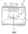
- a current sensor 200includes: a primary conductor 210 having a U-shaped current path 210A; a signal terminal side member 220 (hereinafter simply referred to as "the member 220" in an abbreviated manner) having a support portion 220A for supporting a magneto-electric conversion element 230A (e.g., a hole element) and lead terminals 220B_1 and 220B_2; and an IC chip 230 that is disposed on the support portion 220A and has the magneto-electric conversion element 230A for detecting magnetic flux to be generated by electric current flowing through the current path 210A.
- the current sensor 200is formed by molding the primary conductor 210, the member 220 and the IC chip 230 by means of a resin 240. The remaining part, except for the IC chip 230 and the resin 240, is a current sensor substrate.
- the lead terminals 220B_1indicate lead terminals that are connected to the support portion 220A, whereas the lead terminals 220B_2 indicate lead terminals that are not connected to the support portion 220A. It should be noted that in commonly explaining the lead terminals 220B_1 and 220B_2, the respective lead terminals will be simply referred to as lead terminals 220B.
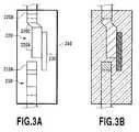
- the current path 210Ais disposed adjacently to the support portion 220A so as not to be overlapped with the support portion 220A in a plan view. Further, as is obvious from a side view of Fig. 3A and a cross-sectional view of Fig. 3B , the support portion 220A and the current path 210A are disposed such that the height of a flat portion of a support portion 220A surface on which the IC chip 230 is mounted is different from that of a flat portion of a current path 210A surface closer to the IC chip 230 in a side view.
- the support portion 220A and the lead terminals 220B_1are not separate members, and are integrally made of a metal material. In other words, the support portion 220A and the lead terminals 220B_1 are physically integrated and are connected to each other not only physically but also electrically.
- the magneto-electric conversion element 230Ais disposed inside the U-shape of the current path 210A in a plan view.
- the IC chip 230is protruded from the support portion 220A in a side view, while being overlapped with the current path 210A in a plan view.
- the member 220has a step portion 220C between the support portion 220A and the lead terminals 220B.
- the step portion 220Cof roughly 20-100 ⁇ m can be produced by means of, for instance, forming of the member 220.
- a clearancecan be thereby obtained between the current path 210A and the IC chip 230.
- the clearancereliably achieves a high insulation and voltage resistance property between the primary conductor 210 and the IC chip 230, and can maintain a high insulation and voltage resistance property in the inside of the package.
- the step portion 220Cdoes not exist, the conductive path 210A of the primary conductor 210 and the IC chip 230 make contact with each other.
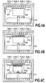
- a lead frameon which a desired pattern is formed, is fabricated from a sheet of metal plate.
- Fig. 4Ashows a part corresponding to a single current sensor.
- the step portion 220Cis produced in the member 220 by means of forming such as stamping ( Fig. 4B ).
- the IC chip 230is die-bonded to the support portion 220B, and thereafter, the lead terminals 220A and the IC chip 230 are wire-bonded ( Fig. 4C ).
- Fig. 5Ais a plan view
- Fig. 5Bis a front view
- Fig. 5Cis a right side view.
- the current sensor 200 according to the first embodimentcan suppress the number of components and reduce manufacturing cost in comparison with a conventional sensor, and in addition, can reliably achieve a high insulation and voltage resistance property between the primary conductor 210 and the IC chip 230.
- Fig. 6Ashows a modification of the current sensor 200 according to the first embodiment. Except for an IC chip 630, a current sensor 600 is the same as the current sensor 200.
- the IC chip 630is designed such that in a plan view, a first magneto-electric conversion element 630A is disposed inside the U-shape of the current path 210A whereas a second magneto-electric conversion element 630B is disposed in a position outside the U-shape of the current path 210A and closer to the current path 210A.
- Fig. 7shows a cross-sectional view of Fig. 6A taken along a line VII-VII.
- the density of magnetic flux to be generated by electric current flowing through the primary conductor in the position of the first magneto-electric conversion element 630Ais set to be B1s, whereas that in the position of the second magneto-electric conversion element 630B is set to be B2s.
- outputs Vo1 and Vo2 of the first magneto-electric conversion element 630A and the second magneto-electric conversion element 630Bare derived as follows.
- Vo 1k 1 ⁇ B 1 s + B 1 n + Vu 1
- Vo 2k 2 ⁇ ⁇ B 2 s + B 2 n + Vu 2 It should be noted that k1 and k2 are sensitivity coefficients of the respective elements, whereas Vu1 and Vu2 are offset values of the respective elements.
- FIG. 6Bshows an example of using three magneto-electric conversion elements as another modification of the current sensor 200 according to the first embodiment.
- a current sensor 700is the same as the current sensor 200 except for an IC chip 730.
- the IC chip 730is designed such that in a plan view, a first magneto-electric conversion element 730A is disposed inside the U-shape of the current path 210A whereas a second magneto-electric conversion element 730B and a third magneto-electric conversion element 730C are disposed in positions outside the both ends of the U-shape of the current path 210A and closer to the current path 210A.
- a current path formed in a C-shape, a V-shape or the like, for instance,may be used for the current path 210A.
- Fig. 8shows a current sensor according to a second embodiment.
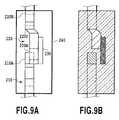
- a current sensor 800is different from the current sensor 200 of the first embodiment in that a support portion 820A of the member 220 has a cutout portion 820A' and the current path 210A is disposed in the cutout portion 820A' in a plan view, although the IC chip 230 is not protruded from the support portion 220A in a side view. Therefore, although not being protruded, the IC chip 230 is overlapped with the current path 210A in a plan view.
- Fig. 9Ashows a side view
- Fig. 9Bshows a cross-sectional view.
- the current path 210Ahaving a height different from that of the current path of the first embodiment in a side view, is disposed in the cutout portion 820A' in a plan view.
- processing of a stamping die for a lead framebecomes slightly complicated.
- the magneto-electric conversion elementcan be flexibly disposed within the IC chip, and thus, can be disposed as inside as possible within the IC chip. Therefore, influence on offset, which is attributed to stress, can be reduced.
- an area in which the support portion and the IC chip are bondedis increased. Hence, the IC chip can be more stably supported.
- the IC chip 230can be set as the IC chip 630 including two magneto-electric conversion elements or the IC chip 730 including three magneto-electric conversion elements.
- Fig. 10shows a current sensor according to a third embodiment.
- a current sensor 1000is different from the current sensor 200 of the first embodiment in that not the member 220 but the primary conductor 210 has a step portion 210C in a position adjacent to the current path 210A.
- the IC chip 230is protruded from the support portion 220A in a side view, while being overlapped with the current path 210A in a plan view.
- Fig. 11Ashows a side view
- Fig. 11Bshows a cross-sectional view.
- the IC chip 230may be set as the IC chip 630 including two magneto-electric conversion elements or the IC chip 730 including three magneto-electric conversion elements.
- the current sensor of the present embodimentis roughly the same as that of the first embodiment shown in Fig. 2 regarding the entire configuration, but is different from that of the first embodiment regarding the configuration having magnetic materials.
- the configuration of the current sensor of the present embodimentwill be hereinafter explained mainly regarding the difference from the configuration of the current sensor of the first embodiment.
- Fig. 12shows an exemplary configuration of a current sensor according to a fourth embodiment.
- the present current sensor 500Aincludes: the primary conductor 210 having the current path 210A formed in a U-shape, for instance, and the conductor terminals 210B; the member 200 having the lead terminals 220B and a support portion 520A for supporting the magneto-electric conversion element 230A; and the IC chip 230 having the magneto-electric conversion element 230A.
- the primary conductor 210, the member 220 and the IC chip 230are molded by means of a resin 240A.
- a magnetic material chip 540 made of a magnetic materialis formed on the IC chip 230 in the present embodiment.
- the support portion 520Ais further configured to support a magnetic material chip 550 made of a magnetic material such as ferrite.
- the support portion 520Ahas, for instance, two step portions 521A and 521B. The shapes of the step portions 521A and 521B will be explained with reference to Fig. 13 to be described.
- the magnetic material chips 540 and 550are disposed such that magnetic flux to be generated by electric current flowing through the current path 210A of the primary conductor 210 is converged on a magneto-sensitive part of the magneto-electric conversion element 230A.
- the current sensor 500Abecomes a current sensor substrate by removing the IC chip 230 and the resin 240A from the aforementioned respective components of the current sensor 500A.
- Fig. 13is a side view of the current sensor 500A of Fig. 12 .
- the step portion 521A of the support portion 520Ais formed such that the middle part of the support portion 520A is upwardly protruded, whereas the step portion 521B is formed such that the tip end of the support portion 520A is more downwardly protruded than the primary conductor 210.
- the magnetic material chip 550is formed on the lower part of the support portion 520A. In other words, the magnetic material chip 550 is formed on the support portion 520A while being separated away from the primary conductor 210.
- the magnetic material chips 540 and 550are formed. Hence, when electric current flows through the current path of the primary conductor 210, magnetic flux to be generated by the electric current becomes likely to be converged on the magneto-sensitive part of the magneto-electric conversion element 230A. Therefore, the current detection sensitivity of the current sensor 500A is enhanced.
- the two magnetic material chips 540 and 550are formed.
- the present embodimentrelates to a current sensor in which the single magnetic chip 540 is only formed, whereby the current detection sensitivity thereof can be enhanced while intrusion of external magnetic field can be inhibited.
- Fig. 14shows an exemplary configuration of the current sensor according to the fifth embodiment.
- the current sensor 500B of the present embodimentincludes: the primary conductor 210 having the current path 210A formed in a U-shape, for instance; the member 220 having the lead terminals 220B and a support portion 520B for supporting the magneto-electric conversion element 230A; and the IC chip 230 having the magneto-electric conversion element 230A.
- the magnetic material chip 540made of a magnetic material is formed on the IC chip 230.
- the primary conductor 210, the member 220 and the IC chip 230are molded by means of the resin 240A.
- the support portion 520B of the present embodimentincludes, for instance, only the single step portion 521A.
- the current sensor 500Bbecomes a current sensor substrate by removing the IC chip 230 and the resin 240A from the aforementioned respective components of the current sensor 500B.
- Fig. 15is a side view of the current sensor 500B shown in Fig. 14 .
- the step portion 521A of the support portion 520Bis formed such that the middle part of the support portion 520B is upwardly protruded.
- the magnetic material chip 540is disposed on the IC chip 230 such that magnetic flux to be generated by electric current flowing through the current path 210A of the primary conductor 210 is converged on the magneto-sensitive part of the magneto-electric conversion element 230A.
- the magnetic material chip 540is formed. Hence, when electric current flows through the current path of the primary conductor 210, magnetic flux to be generated by the electric current becomes likely to be converged on the magneto-sensitive part of the magneto-electric conversion element 230A. Therefore, the current detection sensitivity of the current sensor 500B is enhanced.
- the two magnetic material chips 540 and 550are formed.
- the present embodimentrelates to a current sensor in which the single magnetic chip 550 is only formed, whereby the current detection sensitivity thereof can be enhanced while intrusion of external magnetic field can be inhibited.
- Fig. 16shows an exemplary configuration of the current sensor according to the sixth embodiment.
- the current sensor 500C of the present embodimentincludes: the primary conductor 210 having, for instance, the U-shaped current path 210A; the member 200 having the lead terminals 220B and the support portion 520A for supporting the magneto-electric conversion element 230A; and the IC chip 230 having the magneto-electric conversion element 230A.
- the magnetic material chip 540made of a magnetic material is formed on the lower part of the support portion 520A.
- the primary conductor 210, the member 220 and the IC chip 230are molded by means of the resin 240A.
- the current sensor 500Cbecomes a current sensor substrate by removing the IC chip 230 and the resin 240A from the aforementioned respective components of the current sensor 500C.
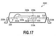
- Fig. 17is a side view of the current sensor 500C shown in Fig. 16 .
- the step portion 521A of the support portion 520Ais formed such that the middle part of the support portion 520A is upwardly protruded
- the step portion 521Bis formed such that the tip end of the support portion 520A is more downwardly protruded than the primary conductor 210.
- the magnetic material chip 550is disposed on the lower part of the support portion 520A such that magnetic flux to be generated by electric current flowing through the current part 210A of the primary conductor 210 is converged on the magneto-sensitive part of the magneto-electric conversion element 230A.
- the magnetic material chip 550is formed. Hence, when electric current flows through the current path of the primary conductor 210, magnetic resistance is reduced and magnetic flux to be generated by the primary conductor current is increased. Therefore, the current detection sensitivity of the current sensor 500C is enhanced.
- the primary conductor 210having, for instance, the U-shaped current path 210A, has been explained as an example.
- the current path 210Amay be configured to have, for instance, any other shape as long as the current sensor functions can be implemented.
- the IC chip 230 having the single magneto-electric conversion elementis applied.
- the IC chipmay be configured to have, for instance, two or more magneto-electric conversion elements. In this case, it is preferable to dispose a magnetic material such that magnetic flux is converged on the magneto-sensitive parts of the respective magneto-electric conversion elements.
- the insulator memberis preferably an insulator tape that is made of a sheet material with a good voltage resistance property and that an adhesive agent is applied to one surface thereof.
- the respective support portions 520A and 520B of the current sensors 500A, 500B and 500C of the respective embodimentshave the step portions.
- the shapes of the step portionscan be changed as long as the height of the support portions can be changed.
- the number of the step portionsmay be three or more as long as the current sensor functions can be implemented.
- Each of the magneto-electric conversion elements of the respective embodimentsmay be either a hole IC including a signal processing circuit or a magnetic resistance IC including a signal processing circuit.
Landscapes
- Engineering & Computer Science (AREA)
- Computer Hardware Design (AREA)
- Microelectronics & Electronic Packaging (AREA)
- Power Engineering (AREA)
- Physics & Mathematics (AREA)
- General Physics & Mathematics (AREA)
- Measuring Instrument Details And Bridges, And Automatic Balancing Devices (AREA)
- Hall/Mr Elements (AREA)
- Measuring Magnetic Variables (AREA)
Description
- The present invention relates to a current sensor substrate and a current sensor, and in more detail, to a current sensor substrate and a current sensor wherein a primary conductor having a U-shaped current path is provided.
- For a current sensor for measuring electric current that flows through a conductor, conventionally known is a method of detecting magnetic flux to be generated by the flow of measurement current in the surrounding of the conductor. For example, in such a method, a magneto-electric conversion element is disposed in the vicinity of a primary conductor through which the measurement current flows.
Fig. 1 (corresponding toFig. 7 in PTL 1) shows an example of a conventional current sensor. A U-shapedcurrent conductor portion 204a is formed in aconductive clip 204, and ahole element 208 is disposed inside the U-shape. Magnetic flux density becomes high in the vicinity of the center of the inside of the U-shape, and thereby, measurement sensitivity is enhanced.- PTL1: Pamphlet of International Patent Publication No.
WO2006/130393 - However, the current sensor shown in
Fig. 1 requires manufacturing efforts such as separately providing theconductive clip 204 and coupling theconductive clip 204 to leadterminals 202a to 202d. This results in cost increase. - The present invention has been produced in view of such a drawback as described above, and it is the first object thereof to reduce manufacturing cost in a current sensor including a primary conductor having a U-shaped current path. Further, it is the second object thereof to provide a substrate for the current sensor.
- To achieve the objects as described above, a first aspect of the present invention relates to a current sensor substrate comprising: a primary conductor having a U-shaped current path; a support portion for supporting a magneto-electric conversion element; and a signal terminal side member having a lead terminal connected to the support portion, and wherein the current path is not overlapped with the support portion in a plan view, while being formed so as to have a height different from a height of the support portion in a side view.
- Moreover, a second aspect of the present invention relates to the first aspect, and wherein the lead terminal may be connected to the support portion through a step.
- Moreover, a third aspect of the present invention relates to the first or second aspect, and wherein the support portion may have a cutout portion, and the current path may be disposed in the cutout portion in a plan view.
- Moreover, a fourth aspect of the present invention relates to the first to third aspects, and wherein the primary conductor may have a step portion connected to the current path.
- A fifth aspect of the present invention relates to any of the first to fourth aspects, and may further comprise a magnetic material disposed so as to be overlapped with the U-shaped current path in a plan view.
- A sixth aspect of the present invention relates to any of the first to fifth aspects, and may further comprise a magnetic material disposed so as to sandwich the U-shaped current path.
- Moreover, a seventh aspect of the present invention may relate to a current sensor comprising: the current sensor substrate recited in any of the first to fourth aspects; and an IC chip that is disposed on the support portion of the current sensor substrate and includes a magneto-electric conversion element for detecting magnetic flux to be generated by electric current flowing through the current path of the current sensor substrate.
- Moreover, an eighth aspect of the present invention relates to the seventh aspect, and wherein the magneto-electric conversion element may be disposed inside the U-shape of the U-shaped current path in a plan view.
- A ninth aspect of the present invention may relate to a current sensor comprising: the current sensor substrate recited in the fifth or sixth aspect; and an IC chip that is disposed on the support portion of the current sensor substrate and includes a magneto-electric conversion element for detecting magnetic flux to be generated by electric current flowing through the current path of the current sensor substrate, and wherein the magneto-electric conversion element is disposed inside the U-shape of the U-shaped current path in a plan view.
- A tenth aspect of the present invention relates to the ninth aspect, and wherein the magnetic material may be formed on an opposite IC chip surface to an IC chip surface on which the U-shaped current path is disposed so as to either partially or entirely cover the magneto-electric conversion element.
- An eleventh aspect of the present invention relates to the ninth or tenth aspect, and wherein the magnetic material may be formed on the support portion so as to be away from the primary conductor.
- A twelfth aspect of the present invention relates to any of the ninth to eleventh aspects, and wherein the magnetic material may be made of either a plated magnetic material or a magnetic chip.
- A thirteenth aspect of the present invention relates to any of the seventh to twelfth aspects, and wherein the IC chip may be protruded from the support portion in a side view.
- A fourteenth aspect of the present invention relates to the thirteenth aspect, and wherein the IC chip may be overlapped with the current path in a plan view, and the magneto-electric conversion element may be disposed inside the U-shape of the U-shaped current path in a plan view.
- A fifteenth aspect of the present invention relates to the thirteenth or fourteenth aspect, and wherein the IC chip may be disposed away from the U-shaped current path at a predetermined interval in a side view.
- A sixteenth aspect of the present invention relates to any of the thirteenth to fifteenth aspects, and wherein the primary conductor may not support the IC chip.
- A seventeenth aspect of the present invention relates to any of the seventh to twelfth aspects, and wherein the support portion of the current sensor substrate may have a cutout portion; and in a plan view, the U-shaped current path of the current sensor substrate may be disposed in the cutout portion while being overlapped with the IC chip.
- An eighteenth aspect of the present invention relates to any of the seventh to seventeenth aspects, and wherein the magneto-electric conversion element may be a hole element.
- A nineteenth aspect of the present invention relates to any of the seventh to eighteenth aspects, and wherein the IC chip may further include a second magneto-electric conversion element disposed in a position outside the U-shape of the current path and closer to the current path.
- A twentieth aspect of the present invention relates to any of the seventh to nineteenth aspects, and wherein the magneto-electric conversion element may be either a hole IC including a signal processing circuit or a magnetic resistance IC including a signal processing circuit.
- A twenty-first aspect of the present invention relates to any of the seventh to twentieth aspects, and may further comprise an insulator member formed between the primary conductor of the current sensor substrate and the IC chip.
- A twenty-second aspect of the present invention relates to the twenty-first aspect, and wherein the insulator member may be an insulator tape.
- According to the present invention, the current sensor substrate is designed to comprise: a primary conductor having a U-shaped current path; a support portion for supporting a magneto-electric conversion element; and a signal terminal side member having a lead terminal connected to the support portion, and wherein the U-shaped current path is not overlapped with the support portion in a plan view, while being formed so as to have a height different from a height of the support portion in a side view. Accordingly, the current sensor substrate and the current sensor can be configured simply and conveniently, while the number of components thereof can be suppressed, and thereby, manufacturing cost can be reduced.
Fig. 1 is a diagram showing a conventional current sensor;Fig. 2 is a diagram showing a current sensor according to a first embodiment;Fig. 3A is a side view of the current sensor shown inFig. 2 ;Fig. 3B is a cross-sectional view ofFig. 2 taken along a line IIIB-IIIB;Fig. 4A is a diagram for explaining a method of manufacturing a current sensor according to anembodiment 1;Fig. 4B is a diagram for explaining the method of manufacturing the current sensor according to theembodiment 1;Fig. 4C is a diagram for explaining the method of manufacturing the current sensor according to theembodiment 1;Fig. 5A is a diagram for explaining the method of manufacturing the current sensor according to theembodiment 1;Fig. 5B is a diagram for explaining the method of manufacturing the current sensor according to theembodiment 1;Fig. 5C is a diagram for explaining the method of manufacturing the current sensor according to theembodiment 1;Fig. 6A is a diagram showing a modification of the current sensor according to theembodiment 1;Fig. 6B is a diagram showing a modification of the current sensor according to theembodiment 1;Fig. 7 is a diagram showing a cross-sectional view ofFig. 6A taken along a line VII-VII;Fig. 8 is a diagram showing a current sensor according to a second embodiment;Fig. 9A is a side view of the current sensor shown inFig. 8 ;Fig. 9B is a cross-sectional view of the current sensor shown inFig. 8 ;Fig. 10 is a diagram showing a current sensor according to a third embodiment;Fig. 11A is a side view of the current sensor shown inFig. 10 ;Fig. 11B is a cross-sectional view of the current sensor shown inFig. 10 ;Fig. 12 is a diagram showing an example of a current sensor according to a fourth embodiment;Fig. 13 is a side view of the current sensor shown inFig. 12 ;Fig. 14 is a diagram showing an example of a current sensor according to a fifth embodiment;Fig. 15 is a side view of the current sensor shown inFig. 14 ;Fig. 16 is a diagram showing an example of a current sensor according to the fifth embodiment; andFig. 17 is a side view of the current sensor shown inFig. 16 .- With reference to the drawings, embodiments of the present invention will be hereinafter explained in detail.
Fig. 2 shows a current sensor according to a first embodiment. Acurrent sensor 200 includes: aprimary conductor 210 having a U-shapedcurrent path 210A; a signal terminal side member 220 (hereinafter simply referred to as "themember 220" in an abbreviated manner) having asupport portion 220A for supporting a magneto-electric conversion element 230A (e.g., a hole element) and lead terminals 220B_1 and 220B_2; and anIC chip 230 that is disposed on thesupport portion 220A and has the magneto-electric conversion element 230A for detecting magnetic flux to be generated by electric current flowing through thecurrent path 210A. Thecurrent sensor 200 is formed by molding theprimary conductor 210, themember 220 and theIC chip 230 by means of aresin 240. The remaining part, except for theIC chip 230 and theresin 240, is a current sensor substrate.- The lead terminals 220B_1 indicate lead terminals that are connected to the
support portion 220A, whereas the lead terminals 220B_2 indicate lead terminals that are not connected to thesupport portion 220A. It should be noted that in commonly explaining the lead terminals 220B_1 and 220B_2, the respective lead terminals will be simply referred to aslead terminals 220B. - The
current path 210A is disposed adjacently to thesupport portion 220A so as not to be overlapped with thesupport portion 220A in a plan view. Further, as is obvious from a side view ofFig. 3A and a cross-sectional view ofFig. 3B , thesupport portion 220A and thecurrent path 210A are disposed such that the height of a flat portion of asupport portion 220A surface on which theIC chip 230 is mounted is different from that of a flat portion of acurrent path 210A surface closer to theIC chip 230 in a side view. - The
support portion 220A and the lead terminals 220B_1 are not separate members, and are integrally made of a metal material. In other words, thesupport portion 220A and the lead terminals 220B_1 are physically integrated and are connected to each other not only physically but also electrically. - As described above, magnetic flux density becomes high in the vicinity of the center of the inside of the U-shape, and accordingly, current detection sensitivity is enhanced. Hence, the magneto-
electric conversion element 230A is disposed inside the U-shape of thecurrent path 210A in a plan view. Moreover, theIC chip 230 is protruded from thesupport portion 220A in a side view, while being overlapped with thecurrent path 210A in a plan view. - In the
current sensor 200 according to the present embodiment, themember 220 has astep portion 220C between thesupport portion 220A and thelead terminals 220B. Thestep portion 220C of roughly 20-100 µm can be produced by means of, for instance, forming of themember 220. A clearance can be thereby obtained between thecurrent path 210A and theIC chip 230. The clearance reliably achieves a high insulation and voltage resistance property between theprimary conductor 210 and theIC chip 230, and can maintain a high insulation and voltage resistance property in the inside of the package. Suppose thestep portion 220C does not exist, theconductive path 210A of theprimary conductor 210 and theIC chip 230 make contact with each other. Even when an insulation sheet is preliminarily attached to the back surface of theIC chip 230, this results in a low insulation and voltage resistance property and electrical breakdown becomes likely to be caused. Moreover, it can be also assumed that an insulation sheet is preliminarily attached to theprimary conductor 210. This results in complication in steps, and thereby, has low chances of becoming reality under the condition that suppress in manufacturing cost is required. - With reference to
Figs. 4A to 4C andFigs. 5A to 5C , explanation will be herein made for a method of manufacturing thecurrent sensor 200 according to anembodiment 1. First, a lead frame, on which a desired pattern is formed, is fabricated from a sheet of metal plate.Fig. 4A shows a part corresponding to a single current sensor. Next, thestep portion 220C is produced in themember 220 by means of forming such as stamping (Fig. 4B ). Then, theIC chip 230 is die-bonded to thesupport portion 220B, and thereafter, thelead terminals 220A and theIC chip 230 are wire-bonded (Fig. 4C ). Finally, theprimary conductor 210, themember 220 and theIC chip 230 are molded by means of theresin 240; lead cutting is performed; and theprimary conductor terminals 210B and the lead terminals (signal terminals) 220B are formed by means of forming.Fig. 5A is a plan view;Fig. 5B is a front view; andFig. 5C is a right side view. - Thus, the
current sensor 200 according to the first embodiment can suppress the number of components and reduce manufacturing cost in comparison with a conventional sensor, and in addition, can reliably achieve a high insulation and voltage resistance property between theprimary conductor 210 and theIC chip 230. Fig. 6A shows a modification of thecurrent sensor 200 according to the first embodiment. Except for anIC chip 630, a current sensor 600 is the same as thecurrent sensor 200. When being disposed on thesupport portion 220A, theIC chip 630 is designed such that in a plan view, a first magneto-electric conversion element 630A is disposed inside the U-shape of thecurrent path 210A whereas a second magneto-electric conversion element 630B is disposed in a position outside the U-shape of thecurrent path 210A and closer to thecurrent path 210A.Fig. 7 shows a cross-sectional view ofFig. 6A taken along a line VII-VII. The density of magnetic flux to be generated by electric current flowing through the primary conductor in the position of the first magneto-electric conversion element 630A is set to be B1s, whereas that in the position of the second magneto-electric conversion element 630B is set to be B2s. Where the densities of magnetic flux to be generated by external magnetic noise in the respective positions are set to be B1n and B2n, outputs Vo1 and Vo2 of the first magneto-electric conversion element 630A and the second magneto-electric conversion element 630B are derived as follows.

- It is herein assumed that variation in characteristics of the both magneto-electric conversion elements is quite small and the relations "k1 = k2 = k" and "Vu1 = Vu2" are established. Further, the distance between the both magneto-electric conversion elements is small, and therefore, approximation is performed as "B1n = B2n". Accordingly, the following is derived.

electric conversion element 630A disposed inside the U-shape is used. Hence, this results in enhancement in sensitivity. - Moreover,
Fig. 6B shows an example of using three magneto-electric conversion elements as another modification of thecurrent sensor 200 according to the first embodiment. A current sensor 700 is the same as thecurrent sensor 200 except for anIC chip 730. When being disposed on thesupport portion 220A, theIC chip 730 is designed such that in a plan view, a first magneto-electric conversion element 730A is disposed inside the U-shape of thecurrent path 210A whereas a second magneto-electric conversion element 730B and a third magneto-electric conversion element 730C are disposed in positions outside the both ends of the U-shape of thecurrent path 210A and closer to thecurrent path 210A. The following is derived where the density of magnetic flux to be generated by electric current flowing through theprimary conductor 210 in the position of the third magneto-electric conversion element 730C is set to be B3s, whereas the density of magnetic flux to be generated by external magnetic noise in the position of the third magneto-electric conversion element 730C is set to be B3n.
primary conductor 210 and theIC chip 730 is displaced in the directions that the three magneto-electric conversion elements are disposed. - Moreover, as a form of the U-shaped current path, a current path formed in a C-shape, a V-shape or the like, for instance, may be used for the
current path 210A. Fig. 8 shows a current sensor according to a second embodiment. Acurrent sensor 800 is different from thecurrent sensor 200 of the first embodiment in that asupport portion 820A of themember 220 has acutout portion 820A' and thecurrent path 210A is disposed in thecutout portion 820A' in a plan view, although theIC chip 230 is not protruded from thesupport portion 220A in a side view. Therefore, although not being protruded, theIC chip 230 is overlapped with thecurrent path 210A in a plan view.Fig. 9A shows a side view, whereasFig. 9B shows a cross-sectional view. Thecurrent path 210A, having a height different from that of the current path of the first embodiment in a side view, is disposed in thecutout portion 820A' in a plan view. Hence, processing of a stamping die for a lead frame becomes slightly complicated. However, the magneto-electric conversion element can be flexibly disposed within the IC chip, and thus, can be disposed as inside as possible within the IC chip. Therefore, influence on offset, which is attributed to stress, can be reduced. Moreover, an area in which the support portion and the IC chip are bonded is increased. Hence, the IC chip can be more stably supported.- It should be noted that similarly to the first embodiment, the
IC chip 230 can be set as theIC chip 630 including two magneto-electric conversion elements or theIC chip 730 including three magneto-electric conversion elements. Fig. 10 shows a current sensor according to a third embodiment. Acurrent sensor 1000 is different from thecurrent sensor 200 of the first embodiment in that not themember 220 but theprimary conductor 210 has astep portion 210C in a position adjacent to thecurrent path 210A. TheIC chip 230 is protruded from thesupport portion 220A in a side view, while being overlapped with thecurrent path 210A in a plan view.Fig. 11A shows a side view, whereasFig. 11B shows a cross-sectional view.- It should be noted that similarly to the first embodiment, the
IC chip 230 may be set as theIC chip 630 including two magneto-electric conversion elements or theIC chip 730 including three magneto-electric conversion elements. - Next, with reference to
Figs. 12 and13 , as an embodiment of the current sensor, explanation will be made for a current sensor that the current detection sensitivity thereof is enhanced while intrusion of external magnetic field can be inhibited. The current sensor of the present embodiment is roughly the same as that of the first embodiment shown inFig. 2 regarding the entire configuration, but is different from that of the first embodiment regarding the configuration having magnetic materials. - The configuration of the current sensor of the present embodiment will be hereinafter explained mainly regarding the difference from the configuration of the current sensor of the first embodiment.
Fig. 12 shows an exemplary configuration of a current sensor according to a fourth embodiment. As shown inFig. 12 , similarly to the current sensor shown inFig. 2 , the presentcurrent sensor 500A includes: theprimary conductor 210 having thecurrent path 210A formed in a U-shape, for instance, and theconductor terminals 210B; themember 200 having thelead terminals 220B and asupport portion 520A for supporting the magneto-electric conversion element 230A; and theIC chip 230 having the magneto-electric conversion element 230A. Theprimary conductor 210, themember 220 and theIC chip 230 are molded by means of aresin 240A.- By contrast, unlike the current sensor shown in
Fig. 2 , amagnetic material chip 540 made of a magnetic material is formed on theIC chip 230 in the present embodiment. Moreover, unlike the current sensor shown inFig. 2 , thesupport portion 520A is further configured to support amagnetic material chip 550 made of a magnetic material such as ferrite. In the present embodiment, thesupport portion 520A has, for instance, twostep portions step portions Fig. 13 to be described. - The
magnetic material chips current path 210A of theprimary conductor 210 is converged on a magneto-sensitive part of the magneto-electric conversion element 230A. - It should be noted that the
current sensor 500A becomes a current sensor substrate by removing theIC chip 230 and theresin 240A from the aforementioned respective components of thecurrent sensor 500A. Fig. 13 is a side view of thecurrent sensor 500A ofFig. 12 . In the presentcurrent sensor 500A, thestep portion 521A of thesupport portion 520A is formed such that the middle part of thesupport portion 520A is upwardly protruded, whereas thestep portion 521B is formed such that the tip end of thesupport portion 520A is more downwardly protruded than theprimary conductor 210.- Further, the
magnetic material chip 550 is formed on the lower part of thesupport portion 520A. In other words, themagnetic material chip 550 is formed on thesupport portion 520A while being separated away from theprimary conductor 210. - In the aforementioned configuration of the
current sensor 500A, themagnetic material chips primary conductor 210, magnetic flux to be generated by the electric current becomes likely to be converged on the magneto-sensitive part of the magneto-electric conversion element 230A. Therefore, the current detection sensitivity of thecurrent sensor 500A is enhanced. - Moreover, with the formation of the
magnetic material chips current sensor 500A. - Next, a fifth embodiment will be explained with reference to
Figs. 14 and15 . - In the fourth embodiment shown in
Figs. 12 and13 , the twomagnetic material chips magnetic chip 540 is only formed, whereby the current detection sensitivity thereof can be enhanced while intrusion of external magnetic field can be inhibited. Fig. 14 shows an exemplary configuration of the current sensor according to the fifth embodiment. Similarly to the current sensor shown inFig. 12 , thecurrent sensor 500B of the present embodiment includes: theprimary conductor 210 having thecurrent path 210A formed in a U-shape, for instance; themember 220 having thelead terminals 220B and asupport portion 520B for supporting the magneto-electric conversion element 230A; and theIC chip 230 having the magneto-electric conversion element 230A. Moreover, similarly to the current sensor shown inFig. 12 , themagnetic material chip 540 made of a magnetic material is formed on theIC chip 230. Theprimary conductor 210, themember 220 and theIC chip 230 are molded by means of theresin 240A.- On the other hand, unlike the current sensor shown in
Fig. 12 , thesupport portion 520B of the present embodiment includes, for instance, only thesingle step portion 521A. - It should be noted that the
current sensor 500B becomes a current sensor substrate by removing theIC chip 230 and theresin 240A from the aforementioned respective components of thecurrent sensor 500B. Fig. 15 is a side view of thecurrent sensor 500B shown inFig. 14 . Similarly to the current sensor shown inFig. 13 , in the presentcurrent sensor 500B, thestep portion 521A of thesupport portion 520B is formed such that the middle part of thesupport portion 520B is upwardly protruded. Moreover, similarly to the current sensor shown inFig. 13 , themagnetic material chip 540 is disposed on theIC chip 230 such that magnetic flux to be generated by electric current flowing through thecurrent path 210A of theprimary conductor 210 is converged on the magneto-sensitive part of the magneto-electric conversion element 230A.- In the aforementioned structure of the
current sensor 500B, themagnetic material chip 540 is formed. Hence, when electric current flows through the current path of theprimary conductor 210, magnetic flux to be generated by the electric current becomes likely to be converged on the magneto-sensitive part of the magneto-electric conversion element 230A. Therefore, the current detection sensitivity of thecurrent sensor 500B is enhanced. - Moreover, with the formation of the
magnetic material chip 540, external magnetic field is supposed to be inhibited from intruding into thecurrent sensor 500B from the upper surface of the package. - Next, a sixth embodiment will be explained with reference to
Figs. 16 and17 . - In the fourth embodiment shown in
Figs. 12 and13 , the twomagnetic material chips magnetic chip 550 is only formed, whereby the current detection sensitivity thereof can be enhanced while intrusion of external magnetic field can be inhibited. Fig. 16 shows an exemplary configuration of the current sensor according to the sixth embodiment. Similarly to the current sensor shown inFig. 12 , thecurrent sensor 500C of the present embodiment includes: theprimary conductor 210 having, for instance, the U-shapedcurrent path 210A; themember 200 having thelead terminals 220B and thesupport portion 520A for supporting the magneto-electric conversion element 230A; and theIC chip 230 having the magneto-electric conversion element 230A. Moreover, similarly to the current sensor shown inFig. 12 , themagnetic material chip 540 made of a magnetic material is formed on the lower part of thesupport portion 520A. Theprimary conductor 210, themember 220 and theIC chip 230 are molded by means of theresin 240A.- It should be noted that the
current sensor 500C becomes a current sensor substrate by removing theIC chip 230 and theresin 240A from the aforementioned respective components of thecurrent sensor 500C. Fig. 17 is a side view of thecurrent sensor 500C shown inFig. 16 . Similarly to the current sensor shown inFig. 13 , in the presentcurrent sensor 500C, thestep portion 521A of thesupport portion 520A is formed such that the middle part of thesupport portion 520A is upwardly protruded, whereas thestep portion 521B is formed such that the tip end of thesupport portion 520A is more downwardly protruded than theprimary conductor 210. Further, similarly to the current sensor shown inFig. 13 , themagnetic material chip 550 is disposed on the lower part of thesupport portion 520A such that magnetic flux to be generated by electric current flowing through thecurrent part 210A of theprimary conductor 210 is converged on the magneto-sensitive part of the magneto-electric conversion element 230A.- In the aforementioned configuration of the
current sensor 500C, themagnetic material chip 550 is formed. Hence, when electric current flows through the current path of theprimary conductor 210, magnetic resistance is reduced and magnetic flux to be generated by the primary conductor current is increased. Therefore, the current detection sensitivity of thecurrent sensor 500C is enhanced. - Moreover, with the formation of the
magnetic material chip 550, external magnetic field is supposed to be inhibited from intruding into thecurrent sensor 500C from the back surface of the package. - The aforementioned current sensors according to the respective embodiments are exemplary only, and can be changed as described below.
- Regarding the
current sensors primary conductor 210 having, for instance, the U-shapedcurrent path 210A, has been explained as an example. However, as another exemplary shape of thecurrent path 210A, thecurrent path 210A may be configured to have, for instance, any other shape as long as the current sensor functions can be implemented. - Regarding the
current sensors IC chip 230 having the single magneto-electric conversion element is applied. However, as an example, the IC chip may be configured to have, for instance, two or more magneto-electric conversion elements. In this case, it is preferable to dispose a magnetic material such that magnetic flux is converged on the magneto-sensitive parts of the respective magneto-electric conversion elements. - Regarding the
current sensors magnetic material chips - Regarding the
current sensors primary conductor 210 and theIC chip 230 so as to cover theprimary conductor 210. For example, the insulator member is preferably an insulator tape that is made of a sheet material with a good voltage resistance property and that an adhesive agent is applied to one surface thereof. - The
respective support portions current sensors - Each of the magneto-electric conversion elements of the respective embodiments may be either a hole IC including a signal processing circuit or a magnetic resistance IC including a signal processing circuit.
- 200
- Current sensor
- 210
- Primary conductor
- 210A
- Current path
- 210B
- Primary conductor terminal
- 210C
- Step portion
- 220
- Signal terminal side member
- 220A
- Support portion
- 220B, 220B_1, 220B_2
- Lead terminal
- 220C
- Step portion
- 230
- IC chip
- 230A
- Magneto-electric conversion element
- 500A, 500B, 500C
- Current sensor
- 520A, 520B
- Step portion
- 630
- IC chip
- 630A
- First magneto-electric conversion element
- 630B
- Second magneto-electric conversion element
- 800
- Current sensor
- 820A
- Support portion
- 820A'
- Cutout portion
- 1000
- Current sensor


Claims (22)
- A current sensor substrate, comprising:a primary conductor (210) having a U-shaped current path (210A) ;a support portion (220A; 520A; 820A) for supporting a magneto-electric conversion element (230A; 630A; 730A); anda lead terminal (220B; 220B_1; 220B_2) connected to the support portion (220A; 520A; 820A);the current sensor substrate beingcharacterised in that the U-shaped current path (210A) is not overlapped with the support portion (220A; 520A; 820A) in a plan view, while being formed so as to have a height different from a height of the support portion (220A; 520A; 820A) in a side view.
- The current sensor substrate recited in claim 1, wherein the lead terminal (220B_1) is connected to the support portion (220A; 520A; 820A) through a step.
- The current sensor substrate recited in claim 1 or 2, wherein the support portion (820A) has a cutout portion (820A'), and
the U-shaped current path (210A) is disposed in the cutout portion (820A') in a plan view. - The current sensor substrate recited in any of claims 1 to 3, wherein the primary conductor (210) has a step portion (210C) connected to the U-shaped current path (210A).
- The current sensor substrate recited in any of claims 1 to 4, further comprising:a magnetic material (540, 550) disposed so as to be overlapped with the U-shaped current path (210A) in a plan view.
- The current sensor substrate recited in claim 5, further comprising:a magnetic material (540, 550) disposed so as to sandwich the U-shaped current path (210A).
- A current sensor (200; 500; 700; 800; 1000), comprising:the current sensor substrate recited in any of claims 1 to 4; andan IC chip (230; 630; 730) disposed on the support portion (220A; 820A) of the current sensor substrate, the IC chip (230; 630; 730) including a magneto-electric conversion element (230A; 630A; 730A) for detecting magnetic flux to be generated by electric current flowing through the U-shaped current path (210A) of the current sensor substrate.
- The current sensor (200; 500; 700; 800; 1000) recited in claim 7, wherein the magneto-electric conversion element (230A; 630A; 730A) is disposed inside the U-shape of the U-shaped current path (210A) in a plan view.
- A current sensor (500), comprising:the current sensor substrate recited in claim 5 or 6; andan IC chip (230) disposed on the support portion (220A; 520A) of the current sensor substrate, the IC chip (230) including a magneto-electric conversion element (230A) for detecting magnetic flux to be generated by electric current flowing through the current path (210A) of the current sensor substrate,wherein the magneto-electric conversion element (230A) is disposed inside the U-shape of the U-shaped current path (210A) in a plan view.
- The current sensor (500) recited in claim 9, wherein the magnetic material (540, 550) is formed on an opposite IC chip surface to an IC chip surface on which the U-shaped current path (210A) is disposed so as to either partially or entirely cover the magneto-electric conversion element (230A).
- The current sensor (500) recited in claim 9 or 10, wherein the magnetic material (540, 550) is formed on the support portion (220A; 520A) so as to be away from the primary conductor (210).
- The current sensor (500) recited in any of claims 9 to 11, wherein the magnetic material is made of either a plated magnetic material or a magnetic chip (540; 550).
- The current sensor (200; 500; 700; 1000) recited in any of claims 7 to 12, wherein the IC chip (230; 630) is protruded from the support portion (220A; 520A; 820A) in a side view.
- The current sensor (200; 500; 700; 800; 1000) recited in claim 13, wherein the IC chip (230; 630; 730) is overlapped with the current path in a plan view, and
the magneto-electric conversion element (230A; 630A; 730A) is disposed inside the U-shape of the U-shaped current path (210A) in a plan view. - The current sensor (200; 500; 700; 800; 1000) recited in claim 13 or 14, wherein the IC chip (230; 630; 730) is disposed away from the U-shaped current path (210A) at a predetermined interval in a side view.
- The current sensor (200; 500; 700; 800; 1000) recited in any of claims 13 to 15, wherein the primary conductor does not support the IC chip (230; 630; 730).
- The current sensor (800) recited in any of claims 7 to 12, wherein the support portion (820A) of the current sensor substrate has a cutout portion (820A'), and
in a plan view, the U-shaped current path (210A) of the current sensor substrate is disposed in the cutout portion (820A') while being overlapped with the IC chip (230). - The current sensor (200; 500; 700; 800; 1000) recited in any of claims 7 to 17, wherein the magneto-electric conversion element is a hole element.
- The current sensor (200; 700) recited in any of claims 7 to 18, wherein the IC chip (230; 630; 730) further includes a second magneto-electric conversion element (630B; 730B) disposed in a position outside the U-shape of the current path and closer to the current path.
- The current sensor (200; 500; 700; 800; 1000) recited in any of claims 7 to 19, wherein the magneto-electric conversion element (230A; 630A; 730A) is either a hole IC including a signal processing circuit or a magnetic resistance IC including a signal processing circuit.
- The current sensor (200; 500; 700; 800; 1000) recited in any of claims 7 to 20, further comprising:an insulator member formed between the primary conductor of the current sensor substrate and the IC chip (230; 630; 730).
- The current sensor (200; 500; 700; 800; 1000) recited in claim 21, wherein the insulator member is an insulator tape.
Applications Claiming Priority (3)
| Application Number | Priority Date | Filing Date | Title |
|---|---|---|---|
| JP2011154658 | 2011-07-13 | ||
| JP2012114392 | 2012-05-18 | ||
| PCT/JP2012/004488WO2013008462A1 (en) | 2011-07-13 | 2012-07-11 | Current sensor substrate and current sensor |
Publications (3)
| Publication Number | Publication Date |
|---|---|
| EP2733496A1 EP2733496A1 (en) | 2014-05-21 |
| EP2733496A4 EP2733496A4 (en) | 2014-12-24 |
| EP2733496B1true EP2733496B1 (en) | 2016-09-07 |
Family
ID=47505765
Family Applications (1)
| Application Number | Title | Priority Date | Filing Date |
|---|---|---|---|
| EP12810990.7AActiveEP2733496B1 (en) | 2011-07-13 | 2012-07-11 | Current sensor substrate and current sensor |
Country Status (7)
| Country | Link |
|---|---|
| US (1) | US9448256B2 (en) |
| EP (1) | EP2733496B1 (en) |
| JP (1) | JP5695195B2 (en) |
| KR (1) | KR101503224B1 (en) |
| CN (1) | CN103649762B (en) |
| TW (1) | TWI480554B (en) |
| WO (1) | WO2013008462A1 (en) |
Families Citing this family (21)
| Publication number | Priority date | Publication date | Assignee | Title |
|---|---|---|---|---|
| US9190606B2 (en)* | 2013-03-15 | 2015-11-17 | Allegro Micosystems, LLC | Packaging for an electronic device |
| US10345343B2 (en) | 2013-03-15 | 2019-07-09 | Allegro Microsystems, Llc | Current sensor isolation |
| TWI504904B (en)* | 2013-07-30 | 2015-10-21 | Asahi Kasei Microdevices Corp | Current sensor |
| JP6294034B2 (en) | 2013-09-05 | 2018-03-14 | ルネサスエレクトロニクス株式会社 | Sensor device |
| JP6234263B2 (en)* | 2014-02-12 | 2017-11-22 | 旭化成エレクトロニクス株式会社 | Current sensor |
| JP6314010B2 (en)* | 2014-03-28 | 2018-04-18 | 旭化成エレクトロニクス株式会社 | Current sensor |
| KR101882126B1 (en)* | 2014-06-27 | 2018-07-25 | 아사히 가세이 일렉트로닉스 가부시끼가이샤 | Current sensor |
| JP2017134022A (en)* | 2016-01-29 | 2017-08-03 | 旭化成エレクトロニクス株式会社 | Electric current sensor and manufacturing method |
| KR102445270B1 (en)* | 2016-12-20 | 2022-09-20 | 한국전자기술연구원 | Current sensor and manufacturing method thereof |
| CN106653999A (en)* | 2016-12-22 | 2017-05-10 | 上海南麟电子股份有限公司 | Single-chip Hall current sensor and preparation method thereof |
| US10698005B2 (en) | 2017-04-20 | 2020-06-30 | Asahi Kasei Microdevices Corporation | Magnetic detection device, current detection device, method for manufacturing magnetic detection device, and method for manufacturing current detection device |
| US10914765B1 (en)* | 2019-07-31 | 2021-02-09 | Allegro Microsystems, Llc | Multi-die integrated current sensor |
| WO2021039264A1 (en)* | 2019-08-26 | 2021-03-04 | 株式会社村田製作所 | Electrical current sensor |
| KR102802251B1 (en)* | 2020-06-18 | 2025-05-07 | 한국전자기술연구원 | High Sensitivity Current Sensor |
| US12345782B2 (en) | 2021-09-29 | 2025-07-01 | Asahi Kasei Microdevices Corporation | Magnetic sensor |
| US11768230B1 (en) | 2022-03-30 | 2023-09-26 | Allegro Microsystems, Llc | Current sensor integrated circuit with a dual gauge lead frame |
| JP7328430B1 (en) | 2022-10-04 | 2023-08-16 | 旭化成エレクトロニクス株式会社 | current sensor |
| JP7329115B1 (en)* | 2022-10-04 | 2023-08-17 | 旭化成エレクトロニクス株式会社 | current sensor |
| JP7328429B1 (en) | 2022-10-04 | 2023-08-16 | 旭化成エレクトロニクス株式会社 | current sensor |
| JP7329118B1 (en) | 2022-10-24 | 2023-08-17 | 旭化成エレクトロニクス株式会社 | current sensor |
| US20240255589A1 (en)* | 2023-01-27 | 2024-08-01 | Asahi Kasei Microdevices Corporation | Magnetic sensor |
Family Cites Families (16)
| Publication number | Priority date | Publication date | Assignee | Title |
|---|---|---|---|---|
| JPS5224404B1 (en)* | 1971-04-29 | 1977-07-01 | ||
| EP0880035B1 (en)* | 1997-05-21 | 2007-05-02 | Sony Manufacturing Systems Corporation | Magnetic metal sensor and method for detecting magnetic metal |
| JP2001165963A (en) | 1999-12-09 | 2001-06-22 | Sanken Electric Co Ltd | Current detecting device |
| JP4164615B2 (en) | 1999-12-20 | 2008-10-15 | サンケン電気株式会社 | CURRENT DETECTOR HAVING HALL ELEMENT |
| JP2001339109A (en)* | 2000-05-26 | 2001-12-07 | Sanken Electric Co Ltd | Current sensing device equipped with hall element |
| US6563299B1 (en) | 2000-08-30 | 2003-05-13 | Micron Technology, Inc. | Apparatus for measuring parasitic capacitance and inductance of I/O leads on an electrical component using a network analyzer |
| JP4471657B2 (en)* | 2001-11-26 | 2010-06-02 | 旭化成エレクトロニクス株式会社 | Current sensor |
| JP2003329749A (en)* | 2002-05-13 | 2003-11-19 | Asahi Kasei Corp | Magnetic sensor and current sensor |
| US20060219436A1 (en)* | 2003-08-26 | 2006-10-05 | Taylor William P | Current sensor |
| US7709754B2 (en)* | 2003-08-26 | 2010-05-04 | Allegro Microsystems, Inc. | Current sensor |
| US7098528B2 (en)* | 2003-12-22 | 2006-08-29 | Lsi Logic Corporation | Embedded redistribution interposer for footprint compatible chip package conversion |
| WO2006010258A1 (en) | 2004-07-27 | 2006-02-02 | University Of Toronto | Tunable magnetic switch |
| TWI312581B (en) | 2006-07-17 | 2009-07-21 | Chipmos Technologies Inc | Chip-on-glass package of image sensor |
| JP5222542B2 (en)* | 2007-12-07 | 2013-06-26 | 矢崎総業株式会社 | Current sensor |
| JP4997146B2 (en)* | 2008-03-05 | 2012-08-08 | 旭化成エレクトロニクス株式会社 | Current sensor |
| JP2014085277A (en)* | 2012-10-25 | 2014-05-12 | Sumitomo Wiring Syst Ltd | Current sensor |
- 2012
- 2012-07-11EPEP12810990.7Apatent/EP2733496B1/enactiveActive
- 2012-07-11WOPCT/JP2012/004488patent/WO2013008462A1/enactiveApplication Filing
- 2012-07-11KRKR1020147000480Apatent/KR101503224B1/enactiveActive
- 2012-07-11JPJP2013523832Apatent/JP5695195B2/enactiveActive
- 2012-07-11CNCN201280034639.0Apatent/CN103649762B/enactiveActive
- 2012-07-11USUS14/131,723patent/US9448256B2/enactiveActive
- 2012-07-13TWTW101125434Apatent/TWI480554B/enactive
Also Published As
| Publication number | Publication date |
|---|---|
| EP2733496A1 (en) | 2014-05-21 |
| US9448256B2 (en) | 2016-09-20 |
| JP5695195B2 (en) | 2015-04-01 |
| KR101503224B1 (en) | 2015-03-16 |
| CN103649762A (en) | 2014-03-19 |
| US20140167736A1 (en) | 2014-06-19 |
| WO2013008462A1 (en) | 2013-01-17 |
| KR20140019470A (en) | 2014-02-14 |
| TWI480554B (en) | 2015-04-11 |
| JPWO2013008462A1 (en) | 2015-02-23 |
| EP2733496A4 (en) | 2014-12-24 |
| TW201314216A (en) | 2013-04-01 |
| CN103649762B (en) | 2015-09-16 |
Similar Documents
| Publication | Publication Date | Title |
|---|---|---|
| EP2733496B1 (en) | Current sensor substrate and current sensor | |
| US9476915B2 (en) | Magnetic field current sensors | |
| US7855546B2 (en) | Current sensor having core with magnetic gap | |
| US10215781B2 (en) | Current sensor | |
| US8760149B2 (en) | Magnetic field current sensors | |
| CN108474810B (en) | Current sensor with integrated primary conductor | |
| JP7387706B2 (en) | Current transducer with integrated primary conductor | |
| US9547024B2 (en) | Device for current measurement | |
| US10290554B2 (en) | Current sensor and method of making a current sensor | |
| JP6256819B2 (en) | Current sensor and current measuring device | |
| JP5695196B2 (en) | Current sensor substrate and current sensor | |
| JP2015152363A (en) | Current sensor | |
| JP6314010B2 (en) | Current sensor | |
| EP3584592A1 (en) | Electronic device and connector | |
| CN113466527A (en) | Sensor device with a bypass current path and corresponding production method | |
| WO2024184224A1 (en) | Magnetic field gradient transducer and current transducer therewith | |
| CN120813846A (en) | Magnetic field gradient sensor and current sensor having the same |
Legal Events
| Date | Code | Title | Description |
|---|---|---|---|
| PUAI | Public reference made under article 153(3) epc to a published international application that has entered the european phase | Free format text:ORIGINAL CODE: 0009012 | |
| 17P | Request for examination filed | Effective date:20140113 | |
| AK | Designated contracting states | Kind code of ref document:A1 Designated state(s):AL AT BE BG CH CY CZ DE DK EE ES FI FR GB GR HR HU IE IS IT LI LT LU LV MC MK MT NL NO PL PT RO RS SE SI SK SM TR | |
| DAX | Request for extension of the european patent (deleted) | ||
| A4 | Supplementary search report drawn up and despatched | Effective date:20141121 | |
| RIC1 | Information provided on ipc code assigned before grant | Ipc:H01L 23/50 20060101ALI20141117BHEP Ipc:G01R 15/20 20060101AFI20141117BHEP Ipc:G01R 15/14 20060101ALI20141117BHEP Ipc:H01L 23/48 20060101ALI20141117BHEP | |
| 17Q | First examination report despatched | Effective date:20141203 | |
| REG | Reference to a national code | Ref country code:DE Ref legal event code:R079 Ref document number:602012022580 Country of ref document:DE Free format text:PREVIOUS MAIN CLASS: G01R0015200000 Ipc:H01L0023000000 | |
| RIC1 | Information provided on ipc code assigned before grant | Ipc:H01L 23/50 20060101ALI20150828BHEP Ipc:H01L 23/48 20060101ALI20150828BHEP Ipc:H01L 23/00 20060101AFI20150828BHEP Ipc:G01R 15/20 20060101ALI20150828BHEP Ipc:G01R 15/14 20060101ALI20150828BHEP | |
| GRAP | Despatch of communication of intention to grant a patent | Free format text:ORIGINAL CODE: EPIDOSNIGR1 | |
| INTG | Intention to grant announced | Effective date:20160322 | |
| GRAS | Grant fee paid | Free format text:ORIGINAL CODE: EPIDOSNIGR3 | |
| GRAA | (expected) grant | Free format text:ORIGINAL CODE: 0009210 | |
| AK | Designated contracting states | Kind code of ref document:B1 Designated state(s):AL AT BE BG CH CY CZ DE DK EE ES FI FR GB GR HR HU IE IS IT LI LT LU LV MC MK MT NL NO PL PT RO RS SE SI SK SM TR | |
| REG | Reference to a national code | Ref country code:GB Ref legal event code:FG4D | |
| REG | Reference to a national code | Ref country code:CH Ref legal event code:EP | |
| REG | Reference to a national code | Ref country code:IE Ref legal event code:FG4D | |
| REG | Reference to a national code | Ref country code:AT Ref legal event code:REF Ref document number:827532 Country of ref document:AT Kind code of ref document:T Effective date:20161015 | |
| REG | Reference to a national code | Ref country code:DE Ref legal event code:R096 Ref document number:602012022580 Country of ref document:DE | |
| REG | Reference to a national code | Ref country code:LT Ref legal event code:MG4D | |
| REG | Reference to a national code | Ref country code:NL Ref legal event code:MP Effective date:20160907 | |
| PG25 | Lapsed in a contracting state [announced via postgrant information from national office to epo] | Ref country code:RS Free format text:LAPSE BECAUSE OF FAILURE TO SUBMIT A TRANSLATION OF THE DESCRIPTION OR TO PAY THE FEE WITHIN THE PRESCRIBED TIME-LIMIT Effective date:20160907 Ref country code:LT Free format text:LAPSE BECAUSE OF FAILURE TO SUBMIT A TRANSLATION OF THE DESCRIPTION OR TO PAY THE FEE WITHIN THE PRESCRIBED TIME-LIMIT Effective date:20160907 Ref country code:FI Free format text:LAPSE BECAUSE OF FAILURE TO SUBMIT A TRANSLATION OF THE DESCRIPTION OR TO PAY THE FEE WITHIN THE PRESCRIBED TIME-LIMIT Effective date:20160907 Ref country code:HR Free format text:LAPSE BECAUSE OF FAILURE TO SUBMIT A TRANSLATION OF THE DESCRIPTION OR TO PAY THE FEE WITHIN THE PRESCRIBED TIME-LIMIT Effective date:20160907 Ref country code:NO Free format text:LAPSE BECAUSE OF FAILURE TO SUBMIT A TRANSLATION OF THE DESCRIPTION OR TO PAY THE FEE WITHIN THE PRESCRIBED TIME-LIMIT Effective date:20161207 | |
| REG | Reference to a national code | Ref country code:AT Ref legal event code:MK05 Ref document number:827532 Country of ref document:AT Kind code of ref document:T Effective date:20160907 | |
| PG25 | Lapsed in a contracting state [announced via postgrant information from national office to epo] | Ref country code:ES Free format text:LAPSE BECAUSE OF FAILURE TO SUBMIT A TRANSLATION OF THE DESCRIPTION OR TO PAY THE FEE WITHIN THE PRESCRIBED TIME-LIMIT Effective date:20160907 Ref country code:NL Free format text:LAPSE BECAUSE OF FAILURE TO SUBMIT A TRANSLATION OF THE DESCRIPTION OR TO PAY THE FEE WITHIN THE PRESCRIBED TIME-LIMIT Effective date:20160907 Ref country code:SE Free format text:LAPSE BECAUSE OF FAILURE TO SUBMIT A TRANSLATION OF THE DESCRIPTION OR TO PAY THE FEE WITHIN THE PRESCRIBED TIME-LIMIT Effective date:20160907 Ref country code:LV Free format text:LAPSE BECAUSE OF FAILURE TO SUBMIT A TRANSLATION OF THE DESCRIPTION OR TO PAY THE FEE WITHIN THE PRESCRIBED TIME-LIMIT Effective date:20160907 Ref country code:GR Free format text:LAPSE BECAUSE OF FAILURE TO SUBMIT A TRANSLATION OF THE DESCRIPTION OR TO PAY THE FEE WITHIN THE PRESCRIBED TIME-LIMIT Effective date:20161208 | |
| PG25 | Lapsed in a contracting state [announced via postgrant information from national office to epo] | Ref country code:RO Free format text:LAPSE BECAUSE OF FAILURE TO SUBMIT A TRANSLATION OF THE DESCRIPTION OR TO PAY THE FEE WITHIN THE PRESCRIBED TIME-LIMIT Effective date:20160907 Ref country code:EE Free format text:LAPSE BECAUSE OF FAILURE TO SUBMIT A TRANSLATION OF THE DESCRIPTION OR TO PAY THE FEE WITHIN THE PRESCRIBED TIME-LIMIT Effective date:20160907 | |
| PG25 | Lapsed in a contracting state [announced via postgrant information from national office to epo] | Ref country code:PL Free format text:LAPSE BECAUSE OF FAILURE TO SUBMIT A TRANSLATION OF THE DESCRIPTION OR TO PAY THE FEE WITHIN THE PRESCRIBED TIME-LIMIT Effective date:20160907 Ref country code:BG Free format text:LAPSE BECAUSE OF FAILURE TO SUBMIT A TRANSLATION OF THE DESCRIPTION OR TO PAY THE FEE WITHIN THE PRESCRIBED TIME-LIMIT Effective date:20161207 Ref country code:SK Free format text:LAPSE BECAUSE OF FAILURE TO SUBMIT A TRANSLATION OF THE DESCRIPTION OR TO PAY THE FEE WITHIN THE PRESCRIBED TIME-LIMIT Effective date:20160907 Ref country code:BE Free format text:LAPSE BECAUSE OF FAILURE TO SUBMIT A TRANSLATION OF THE DESCRIPTION OR TO PAY THE FEE WITHIN THE PRESCRIBED TIME-LIMIT Effective date:20160907 Ref country code:IS Free format text:LAPSE BECAUSE OF FAILURE TO SUBMIT A TRANSLATION OF THE DESCRIPTION OR TO PAY THE FEE WITHIN THE PRESCRIBED TIME-LIMIT Effective date:20170107 Ref country code:AT Free format text:LAPSE BECAUSE OF FAILURE TO SUBMIT A TRANSLATION OF THE DESCRIPTION OR TO PAY THE FEE WITHIN THE PRESCRIBED TIME-LIMIT Effective date:20160907 Ref country code:SM Free format text:LAPSE BECAUSE OF FAILURE TO SUBMIT A TRANSLATION OF THE DESCRIPTION OR TO PAY THE FEE WITHIN THE PRESCRIBED TIME-LIMIT Effective date:20160907 Ref country code:CZ Free format text:LAPSE BECAUSE OF FAILURE TO SUBMIT A TRANSLATION OF THE DESCRIPTION OR TO PAY THE FEE WITHIN THE PRESCRIBED TIME-LIMIT Effective date:20160907 Ref country code:PT Free format text:LAPSE BECAUSE OF FAILURE TO SUBMIT A TRANSLATION OF THE DESCRIPTION OR TO PAY THE FEE WITHIN THE PRESCRIBED TIME-LIMIT Effective date:20170109 | |
| REG | Reference to a national code | Ref country code:DE Ref legal event code:R097 Ref document number:602012022580 Country of ref document:DE | |
| PG25 | Lapsed in a contracting state [announced via postgrant information from national office to epo] | Ref country code:IT Free format text:LAPSE BECAUSE OF FAILURE TO SUBMIT A TRANSLATION OF THE DESCRIPTION OR TO PAY THE FEE WITHIN THE PRESCRIBED TIME-LIMIT Effective date:20160907 | |
| PLBE | No opposition filed within time limit | Free format text:ORIGINAL CODE: 0009261 | |
| STAA | Information on the status of an ep patent application or granted ep patent | Free format text:STATUS: NO OPPOSITION FILED WITHIN TIME LIMIT | |
| PG25 | Lapsed in a contracting state [announced via postgrant information from national office to epo] | Ref country code:DK Free format text:LAPSE BECAUSE OF FAILURE TO SUBMIT A TRANSLATION OF THE DESCRIPTION OR TO PAY THE FEE WITHIN THE PRESCRIBED TIME-LIMIT Effective date:20160907 | |
| 26N | No opposition filed | Effective date:20170608 | |
| PG25 | Lapsed in a contracting state [announced via postgrant information from national office to epo] | Ref country code:SI Free format text:LAPSE BECAUSE OF FAILURE TO SUBMIT A TRANSLATION OF THE DESCRIPTION OR TO PAY THE FEE WITHIN THE PRESCRIBED TIME-LIMIT Effective date:20160907 | |
| REG | Reference to a national code | Ref country code:CH Ref legal event code:PL | |
| GBPC | Gb: european patent ceased through non-payment of renewal fee | Effective date:20170711 | |
| REG | Reference to a national code | Ref country code:IE Ref legal event code:MM4A | |
| REG | Reference to a national code | Ref country code:FR Ref legal event code:ST Effective date:20180330 | |
| PG25 | Lapsed in a contracting state [announced via postgrant information from national office to epo] | Ref country code:LI Free format text:LAPSE BECAUSE OF NON-PAYMENT OF DUE FEES Effective date:20170731 Ref country code:CH Free format text:LAPSE BECAUSE OF NON-PAYMENT OF DUE FEES Effective date:20170731 Ref country code:GB Free format text:LAPSE BECAUSE OF NON-PAYMENT OF DUE FEES Effective date:20170711 Ref country code:IE Free format text:LAPSE BECAUSE OF NON-PAYMENT OF DUE FEES Effective date:20170711 | |
| PG25 | Lapsed in a contracting state [announced via postgrant information from national office to epo] | Ref country code:FR Free format text:LAPSE BECAUSE OF NON-PAYMENT OF DUE FEES Effective date:20170731 | |
| PG25 | Lapsed in a contracting state [announced via postgrant information from national office to epo] | Ref country code:LU Free format text:LAPSE BECAUSE OF NON-PAYMENT OF DUE FEES Effective date:20170711 | |
| PG25 | Lapsed in a contracting state [announced via postgrant information from national office to epo] | Ref country code:MT Free format text:LAPSE BECAUSE OF NON-PAYMENT OF DUE FEES Effective date:20170711 | |
| PG25 | Lapsed in a contracting state [announced via postgrant information from national office to epo] | Ref country code:AL Free format text:LAPSE BECAUSE OF FAILURE TO SUBMIT A TRANSLATION OF THE DESCRIPTION OR TO PAY THE FEE WITHIN THE PRESCRIBED TIME-LIMIT Effective date:20160907 | |
| PG25 | Lapsed in a contracting state [announced via postgrant information from national office to epo] | Ref country code:HU Free format text:LAPSE BECAUSE OF FAILURE TO SUBMIT A TRANSLATION OF THE DESCRIPTION OR TO PAY THE FEE WITHIN THE PRESCRIBED TIME-LIMIT; INVALID AB INITIO Effective date:20120711 Ref country code:MC Free format text:LAPSE BECAUSE OF FAILURE TO SUBMIT A TRANSLATION OF THE DESCRIPTION OR TO PAY THE FEE WITHIN THE PRESCRIBED TIME-LIMIT Effective date:20160907 | |
| PG25 | Lapsed in a contracting state [announced via postgrant information from national office to epo] | Ref country code:CY Free format text:LAPSE BECAUSE OF NON-PAYMENT OF DUE FEES Effective date:20160907 | |
| PG25 | Lapsed in a contracting state [announced via postgrant information from national office to epo] | Ref country code:MK Free format text:LAPSE BECAUSE OF FAILURE TO SUBMIT A TRANSLATION OF THE DESCRIPTION OR TO PAY THE FEE WITHIN THE PRESCRIBED TIME-LIMIT Effective date:20160907 | |
| PG25 | Lapsed in a contracting state [announced via postgrant information from national office to epo] | Ref country code:TR Free format text:LAPSE BECAUSE OF FAILURE TO SUBMIT A TRANSLATION OF THE DESCRIPTION OR TO PAY THE FEE WITHIN THE PRESCRIBED TIME-LIMIT Effective date:20160907 | |
| P01 | Opt-out of the competence of the unified patent court (upc) registered | Effective date:20230515 | |
| PGFP | Annual fee paid to national office [announced via postgrant information from national office to epo] | Ref country code:DE Payment date:20240529 Year of fee payment:13 |