EP2728757B1 - Wideband software-defined RF receiver - Google Patents
Wideband software-defined RF receiverDownload PDFInfo
- Publication number
- EP2728757B1 EP2728757B1EP20120190977EP12190977AEP2728757B1EP 2728757 B1EP2728757 B1EP 2728757B1EP 20120190977EP20120190977EP 20120190977EP 12190977 AEP12190977 AEP 12190977AEP 2728757 B1EP2728757 B1EP 2728757B1
- Authority
- EP
- European Patent Office
- Prior art keywords
- signal
- processing unit
- frequency band
- intermediate frequency
- bypass
- Prior art date
- Legal status (The legal status is an assumption and is not a legal conclusion. Google has not performed a legal analysis and makes no representation as to the accuracy of the status listed.)
- Active
Links
- 238000012545processingMethods0.000claimsdescription69
- 238000000034methodMethods0.000claimsdescription11
- 230000002452interceptive effectEffects0.000claimsdescription9
- 238000004590computer programMethods0.000claimsdescription6
- 238000010586diagramMethods0.000description6
- 238000001914filtrationMethods0.000description5
- 238000010845search algorithmMethods0.000description3
- 238000013459approachMethods0.000description2
- 238000006243chemical reactionMethods0.000description2
- 230000000694effectsEffects0.000description2
- 238000005516engineering processMethods0.000description2
- 230000003044adaptive effectEffects0.000description1
- 230000000295complement effectEffects0.000description1
- 238000012937correctionMethods0.000description1
- 230000001419dependent effectEffects0.000description1
- 230000010354integrationEffects0.000description1
- 238000002955isolationMethods0.000description1
- 239000004065semiconductorSubstances0.000description1
Images


Classifications
- H—ELECTRICITY
- H04—ELECTRIC COMMUNICATION TECHNIQUE
- H04B—TRANSMISSION
- H04B1/00—Details of transmission systems, not covered by a single one of groups H04B3/00 - H04B13/00; Details of transmission systems not characterised by the medium used for transmission
- H04B1/0003—Software-defined radio [SDR] systems, i.e. systems wherein components typically implemented in hardware, e.g. filters or modulators/demodulators, are implented using software, e.g. by involving an AD or DA conversion stage such that at least part of the signal processing is performed in the digital domain
- H04B1/0007—Software-defined radio [SDR] systems, i.e. systems wherein components typically implemented in hardware, e.g. filters or modulators/demodulators, are implented using software, e.g. by involving an AD or DA conversion stage such that at least part of the signal processing is performed in the digital domain wherein the AD/DA conversion occurs at radiofrequency or intermediate frequency stage
- H04B1/0021—Decimation, i.e. data rate reduction techniques
- H—ELECTRICITY
- H04—ELECTRIC COMMUNICATION TECHNIQUE
- H04B—TRANSMISSION
- H04B1/00—Details of transmission systems, not covered by a single one of groups H04B3/00 - H04B13/00; Details of transmission systems not characterised by the medium used for transmission
- H04B1/0003—Software-defined radio [SDR] systems, i.e. systems wherein components typically implemented in hardware, e.g. filters or modulators/demodulators, are implented using software, e.g. by involving an AD or DA conversion stage such that at least part of the signal processing is performed in the digital domain
- H04B1/0007—Software-defined radio [SDR] systems, i.e. systems wherein components typically implemented in hardware, e.g. filters or modulators/demodulators, are implented using software, e.g. by involving an AD or DA conversion stage such that at least part of the signal processing is performed in the digital domain wherein the AD/DA conversion occurs at radiofrequency or intermediate frequency stage
- H04B1/001—Channel filtering, i.e. selecting a frequency channel within the SDR system
- H—ELECTRICITY
- H04—ELECTRIC COMMUNICATION TECHNIQUE
- H04B—TRANSMISSION
- H04B1/00—Details of transmission systems, not covered by a single one of groups H04B3/00 - H04B13/00; Details of transmission systems not characterised by the medium used for transmission
- H04B1/06—Receivers
- H04B1/10—Means associated with receiver for limiting or suppressing noise or interference
Definitions
- the present inventionrelates to the field of software-defined RF receivers, in particular to wideband software-defined RF receivers with adaptive reception technology.
- analog filter circuitryis used to select the wanted intermediate frequency (IF) band prior to performing analog-to-digital conversion and demodulation.
- This analog filter circuitryis expensive and in many cases difficult to integrate with the digital circuitry, e.g. in VLSI (very-large-scale integration) CMOS (complementary metal-oxide-semiconductor) designs.
- an RF receivercomprises (a) an analog-to-digital converter for converting an analog intermediate frequency band signal to a digital intermediate frequency band signal, (b) a plurality of decimation units coupled in cascade for generating a decimated signal based on the digital intermediate frequency band signal, (c) a signal processing unit for processing the decimated signal, and (d) a bypass path for feeding a bypass signal to the signal processing unit, the bypass signal being either the digital intermediate frequency band signal or an output signal from one of the decimation units which is not the last one of the cascade coupled decimation units, wherein the signal processing unit is (e) adapted to detect critical reception conditions based on the bypass signal and (f) to adapt the processing of the decimated signal in accordance with detected critical reception conditions.
- This aspectis based on the idea that by analyzing a bypass signal, i.e. the digital intermediate frequency band signal output by the analog-to-digital converter (ADC) or a not fully decimated signal derived from the output of the ADC, critical or potentially disturbing signal content occurring somewhere in the wideband (intermediate frequency band) digital signal which is output by the ADC can be detected and taken into consideration at the processing stage. Thereby, a robust RF receiver can be provided at a relatively low price.
- ADCanalog-to-digital converter
- analog intermediate frequency band signalmay particularly denote an analog output signal from an RF mixer stage including filtering, the RF mixer stage being designed to provide an intermediate frequency (IF) band signal with a bandwidth corresponding to the bandwidth of interest, i.e. the total bandwidth in which the RF receiver is intended to receive signals.
- the bandwidth of the analog intermediate frequency band signalis so large that it encompasses a wide range of frequency bands of interest, i.e. a wide range of narrow frequency bands each of which contains a particular signal of interest, such as e.g. a particular radio station.
- the analog intermediate frequency band signaldoes not merely have a bandwidth corresponding to a single signal of interest but rather a bandwidth extending over a wide range of frequencies of interest.
- the analog-to-digital converteris preferably a wideband sigma-delta ADC capable of converting the analog intermediate frequency band signal into a corresponding digital intermediate frequency band signal, i.e. a digital signal with a bandwidth substantially equal to the bandwidth of the analog intermediate frequency band signal.
- the ADCis adapted to sample the analog intermediate frequency band signal with a sample rate which is sufficiently high to substantially maintain the bandwidth of the analog signal.
- decimation unitmay particularly denote a unit comprising an anti-aliasing filter and a downconverter for reducing the sample rate of a digital signal input to the decimation unit.
- decimation units coupled in cascademay particularly denote that the output of a first decimation unit is coupled to the input of a second decimation unit, the output of the second decimation unit is coupled to the input of a third decimation unit, and so forth.
- the cascade coupled decimation unitsreduces the sample rate of the input signal step by step.
- decimated signalmay particularly denote the output from the last one of the cascade coupled decimation units, i.e. the decimation unit which provides the last step of the decimation. Accordingly, the decimated signal will have a reduced sample rate (and thus also a reduced bandwidth) in comparison to the digital intermediate frequency band signal.
- signal processing unitmay particularly denote a processing unit comprising a software-defined-radio (SDR) processor and demodulation circuitry.
- SDRsoftware-defined-radio
- critical reception conditionsmay particularly denote signal content within the intermediate frequency band which (due to various effects resulting from the analog and/or digital processing of the signal on its way from the RF input to the signal processing unit) may cause undesirable signal content to occur within the baseband processed by the signal processing unit. Such undesirable signal content in the baseband may cause errors in the final decoded signal or even make it impossible to decode the signal.
- bypass path and the signal processing unitincurs significantly less cost than the provision of the high quality analog bandpass filter circuitry used in conventional receivers.
- the RF receiverfurther comprises a digital channel filter arranged between the cascade coupled decimation units and the signal processing unit.
- digital channel filtermay particularly denote a digital filter or digital filter bank which is capable of letting through only signal content within one or more narrow bands (channels, corresponding e.g. to frequency bands where radio stations are supposed to be present).
- the digital channel filterserves to provide only the signal content falling within the channel(s) which is/are of interest to the signal processing unit.
- each of the decimation unitsis adapted to reduce a sample rate by a rational fraction or by an integer factor.
- rational fractionmay particularly denote a rational number, such as m/n, where both m and n are integers and n>m.
- each decimation unitmay apply the same rational fraction or integer factor, whereas in other embodiments, at least some of the decimation units may apply different rational fractions or integer factors.
- the signal processing unitis adapted to detect critical reception conditions by detecting the presence in the bypass signal of at least one of (a) a spurious interference signal, (b) a DC artefact signal, (c) an image signal, and (d) a harmonic of an unwanted signal.
- the term "spurious interference signal”may in particular denote an unwanted signal component occurring within the frequency band of interest due to e.g. insufficient electrical isolation
- DC artefact signalmay in particular denote unwanted signal content caused by active circuitry and occurring around a local oscillator frequency in the mixing/tuning stage of the receiver. This unwanted signal content accordingly occurs around the frequency 0 Hz at IF level and may fall into a wanted frequency band, thereby compromising baseband decoding in the signal processing unit.
- image signalmay in particular denote signal content falling within the desired frequency band as a result of frequency conversion or decimation.
- harmonic of an unwanted signalmay in particular denote unwanted signal content within the desired frequency band, which is a harmonic (i.e. 2 nd , 3 rd , ... n th harmonic) of a strong unwanted signal located outside the desired frequency band.
- the signal processing unitis adapted to detect the critical reception conditions by analyzing a FFT (i.e. a fast-Fourier transform) of the bypass signal.
- FFTi.e. a fast-Fourier transform
- the signal processing unitmay determine whether one of the above mentioned types of unwanted signals (or other unwanted signals) may cause problems within the desired frequency band.
- the FFThas a resolution in the range of 50 kHz to 500 kHz, such as in the range of 100 kHz to 400 kHz, such as in the range of 200 kHz to 300 kHz, such as around 250 kHz.
- Such a coarse FFT analysiscan easily be performed by the signal processing unit in parallel with the main processing of the signal without noticeable impact for the user.
- the signal processing unitis adapted to adjust tuning such that a wanted signal or an interfering signal is displaced within the intermediate frequency band.
- Thismay e.g. be achieved by outputting a control signal to a local oscillator such that the latter changes its frequency.
- the signal processing unitis adapted to remove an interfering signal by applying a notch filter.
- the intermediate frequency bandhas a bandwidth of at least 10 MHz, such as 20 MHz, such as 30 MHz, such as 40 MHz, such as 50 MHz, such as 60 MHz, such as 70 MHz, such as 80 MHz, such as 90 MHz, or such as 100 MHz.
- the intermediate frequency bandmay preferably have a bandwidth of 40 MHz.
- a DAB (Digital Audio Broadcasting) radio apparatuscomprising an RF receiver according to the first aspect or any of the above embodiments.
- the DAB radio apparatusbenefits from the advantages described above with regard to the first aspect and the related embodiments.
- the DAB radio apparatusis among others capable of simultaneously receiving and decoding several broadcast signals (e.g. radio stations) and of performing background search algorithms for alternative stations without the necessity of expensive analog filtering circuitry.
- a method of receiving RF signalscomprises (a) converting an analog intermediate frequency band signal to a digital intermediate frequency band signal, (b) generating a decimated signal based on the digital intermediate frequency band signal using a plurality of decimation units coupled in cascade, (c) processing the decimated signal at a signal processing unit, (d) feeding a bypass signal to the signal processing unit via a bypass path, the bypass signal being either the digital intermediate frequency band signal or an output signal from one of the decimation units which is not the last one of the cascade coupled decimation units, and, at the signal processing unit, (e) detecting critical reception conditions based on the bypass signal and (f) adapting the processing of the decimated signal in accordance with detected critical reception conditions.
- this third aspectmay be based on the idea that by analyzing a bypass signal, i.e. the digital intermediate frequency band signal output by the analog-to-digital converter (ADC) or a not fully decimated signal derived from the output of the ADC, critical or potentially disturbing signal content occurring somewhere in the wideband (intermediate frequency band) digital signal which is output by the ADC can be detected and taken into consideration at the processing stage. Thereby, robust RF signal reception can be provided at a relatively low price.
- ADCanalog-to-digital converter
- the methodmay preferably be implemented in a device according to the first aspect and any of the embodiments thereof as described above.
- a computer programcomprising computer executable instructions which when executed by a computer causes the computer to perform the steps of the method according to the third aspect.
- the computermay preferably be or comprise a software-defined radio processor.
- a computer program productcomprising a computer readable data carrier loaded with a computer program according to the fourth aspect.
- FIG. 1shows a block diagram of a conventional RF receiver 1.
- the receiver 1comprises an RF filter 3 which receives an RF input signal 2 from an antenna (not shown).
- the RF filter 3is a band-pass filter designed to let signal content within a certain frequency range pass through it.
- the filtered signalis amplified by low noise amplifier 4 and forwarded to an RF I/Q-mixer 5 which generates in-phase (I) and quadrature-phase (Q) signals and forwards these through IF filter 6.
- the IF filter 6is an analog pass-band filter with a relatively narrow pass-band surrounding the frequency range where a desired signal content is located.
- the filtered IF-signalis amplified by IF amplifier 7 and converted to a digital signal by ADC 8.
- the ADC 8has a sample rate at least fulfilling the Nyquist criteria such that the full bandwidth of the filtered analog IF-signal is maintained in the converted digital signal.
- the digital signalis demodulated by hardware demodulator 9 in order to obtain the desired signal content.
- the stipulated line 10surrounds the elements which are formed as an integrated circuit. More specifically, the integrated circuit 10 comprises the low noise amplifier 4, the I/Q mixer 5, the IF filter 6, the IF amplifier 7, the ADC 8 and the demodulator 9.
- a conventional RF receiver 1 as the one shown in Figure 1performs a significant part of the processing in the analog domain while only the wanted narrowband signal is processed in the digital domain.
- This analog processingin particular filtering, is associated with high cost and effort and is difficult to implement in certain technologies, such as e.g. VLSI CMOS.
- simultaneous reception of several channels or parallel searching for alternative stationsrequires additional analog filtering circuitry and thus increases the costs even further.
- FIG 2shows a block diagram of a general software-defined RF receiver 200, i.e. a receiver where the majority of the processing takes place in the digital domain by means of a programmable signal processing unit 228.
- the software-defined RF receiver 200comprises an RF input filter 210 and an integrated circuit 220 comprising the remaining receiver components.
- the RF filter 210is a less costly coarse RF filter with a wider passband.
- the integrated circuit 220comprises the remaining receiver components, i.e. low noise amplifier 221, RF I/Q mixer 222, coarse IF filter 223, IF amplifier 224, wideband sigma-delta ADC 225, decimation units 226, digital channel filter 227, and a signal processing unit 228.
- the signal processing unit 228comprises a software-defined radio processor and demodulation circuitry.
- the RF filter 210receives an RF input signal 211 from e.g. an antenna (not shown) and forwards the pass-band filtered RF signal to an input of the integrated circuit 220, where it is amplified by the low noise amplifier 221 and then mixed to an intermediate frequency (IF) band by I/Q mixer 222 and IF filter 223 and finally amplified by IF amplifier 224.
- IFintermediate frequency
- the resulting analog intermediate frequency band signalhas a significantly larger bandwidth. If the receiver 200 is to be used in a DAB radio apparatus the IF bandwidth may e.g. be around 40 MHz.
- the hitherto described analog part of the receiver 200differs from the corresponding part of the conventional receiver 1 shown in Figure 1 mainly in the RF filter 210 and in particular the IF filter 223 have much larger bandwidths than the corresponding RF-filter 3 and IF filter 6 of the conventional RF receiver 1 shown in Figure 1 (i.e. they are coarse filters in comparison). This fact already reduces the cost of the analog components of the receiver 200 significantly.
- the sigma-delta ADC 225converts the wideband digital intermediate frequency band signal output by the IF amplifier 224 to a corresponding wideband digital intermediate frequency band signal.
- This digital signalis then run through a cascade of decimation units 226 which step by step reduces the sample rate (and thereby the bandwidth) of the digital signal.
- Figure 2shows two decimation units 326. However, it is explicitly noted that more (i.e. 3, 4, 5, 6 or even more) decimation units 326 may be provided.
- a desired narrow frequency band (channel)is selected by digital channel filter 227 and forwarded to the signal processing unit 228 where the desired signal content is extracted (decoded) by the software-defined radio processor and demodulator circuitry.
- the narrow-band signal processed by the signal processing unit 228may in addition to the wanted signal content also contain unwanted signal content originating from various hardware effects. Such unwanted signal content may severely degrade the receiver performance or even make decoding of the wanted signal content impossible. Examples of unwanted signal content include (but is not limited to) spurious signals interfering with the wanted signal content, DC artefact signals, image signals, and harmonics of other signals. As the signal processing unit 227 only receives the wanted narrow frequency band after decimation and channel filtering of the intermediate frequency band signal, the processing unit 228 is unable to distinguish wanted and unwanted signal content from each other.
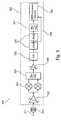
- FIG 3shows a block diagram of an improved software-defined RF receiver 300 in accordance with an embodiment of the present invention.
- the improved receiver 300is capable of overcoming the above mentioned drawbacks of the receiver 200 shown in Figure 2 , i.e. in particular the negative impact of unwanted signal content originating from the wide intermediate frequency band.
- the structure and elements of the receiver 300correspond in so far as nothing else is explicitly stated in the following to the structure and elements of the receiver 200 shown in Figure 2 and described in detail above. For reasons of brevity, the description of the corresponding structure and elements will not be repeated.
- the receiver 300differs from the receiver 200 in two points.
- the first pointis the bypass path 329 between the output of the first decimation unit 326 of the cascade coupled decimation units 326 and the signal processing unit 328.
- the second pointis that the signal processing unit 328 is adapted to process and analyze the bypass signal provided via the bypass path 329.
- the specific arrangement of the bypass path 329 shown in Figure 3is exemplary.
- the purpose of the bypass path 329is to bypass at least a part (or even all) of the cascaded decimation units 326 as well as the channel filter 327 and thereby provide (almost) the entire IF band signal to the signal processing unit.
- the signal processing unit 328will be able to identify potentially critical signal content within the IF band which may have a negative impact on the reception quality.
- the identification of potentially critical signal contentis performed by applying a FFT to the bypass signal.
- the FFTcan be applied without interrupting the RF signal, i.e. in parallel with the reception processing, and if necessary, the FFT can be applied while the RF input 311 is momentarily shut off.
- the duration of the momentary shut off of the RF inputis about 1/ ⁇ f, where ⁇ f denotes the frequency resolution of the FFT.
- the duration of the momentary shut off of the RF signal 311is so short that it does not have any noticeable impact on the receiver performance.
- the FFThas a resolution of 250 kHz, corresponding to a duration of about 4 ⁇ s of the momentary shut off of the RF signal 311.
- spurious signals and DC artefactswhich will interfere with or mask the wanted signal content can be detected.
- signal content in frequency bands which causes disturbing image signals or harmonics within the frequency band of the wanted signalcan be detected.
- spurious signals and DC artefactscan in many cases best be detected by shortly interrupting the RF signal 311, whereas e.g. unwanted image signals and harmonics are best detected without shutting off the RF signal 311 while applying the FFT to the bypass signal.
- the signal processing unit 328can react accordingly. For example, in the case of a spurious signal interfering with the wanted signal, the signal processing unit 328 will send a control signal to the I/Q mixer 322 and/or the IF filter 323 to adjust tuning (i.e. the frequency of a local oscillator) such that the interfering signal is shifted (displaced) to a position outside the wanted frequency band. Similar strategies are applicable in case of DC artefacts, image signals and harmonic signals. As an alternative or addition to the aforementioned tuning adjustment, a notch filter can be used to remove the interfering signal component in the baseband processing performed by the signal processing unit 328.
Landscapes
- Engineering & Computer Science (AREA)
- Computer Networks & Wireless Communication (AREA)
- Signal Processing (AREA)
- Noise Elimination (AREA)
- Circuits Of Receivers In General (AREA)
Description
- The present invention relates to the field of software-defined RF receivers, in particular to wideband software-defined RF receivers with adaptive reception technology.
- In conventional RF-receivers, analog filter circuitry is used to select the wanted intermediate frequency (IF) band prior to performing analog-to-digital conversion and demodulation. This analog filter circuitry is expensive and in many cases difficult to integrate with the digital circuitry, e.g. in VLSI (very-large-scale integration) CMOS (complementary metal-oxide-semiconductor) designs.
- With the increasing availability of low-cost powerful digital signal processors and wideband analog-to-digital converters (ADCs) it has become feasible to omit the expensive and often complex analog filter circuitry and instead sample and process large parts of the reception bands at once. Apart from the cost reduction, new features, such as e.g. simultaneous reception of multiple broadcasts and background search algorithms for alternative radio stations, can be realized with this approach.
US 2005/0276531 andUS 2012/0163517 disclose receiving arrangements including a decimation unit. - However, due to the wide passband of such a receiver, signal content outside a particular wanted frequency band may have a negative influence on the signal content within the wanted frequency band and thereby lead to difficult conditions at the final demodulation stage.
- There may thus be a need for an improved wideband RF-receiver which is capable of dealing with the above problems.
- This need may be met by the subject matter according to the independent claims. Advantageous embodiments of the present invention are set forth in the dependent claims.
- According to a first aspect there is provided an RF receiver. The described RF receiver comprises (a) an analog-to-digital converter for converting an analog intermediate frequency band signal to a digital intermediate frequency band signal, (b) a plurality of decimation units coupled in cascade for generating a decimated signal based on the digital intermediate frequency band signal, (c) a signal processing unit for processing the decimated signal, and (d) a bypass path for feeding a bypass signal to the signal processing unit, the bypass signal being either the digital intermediate frequency band signal or an output signal from one of the decimation units which is not the last one of the cascade coupled decimation units, wherein the signal processing unit is (e) adapted to detect critical reception conditions based on the bypass signal and (f) to adapt the processing of the decimated signal in accordance with detected critical reception conditions.
- This aspect is based on the idea that by analyzing a bypass signal, i.e. the digital intermediate frequency band signal output by the analog-to-digital converter (ADC) or a not fully decimated signal derived from the output of the ADC, critical or potentially disturbing signal content occurring somewhere in the wideband (intermediate frequency band) digital signal which is output by the ADC can be detected and taken into consideration at the processing stage. Thereby, a robust RF receiver can be provided at a relatively low price.
- In the present context, the term "analog intermediate frequency band signal" may particularly denote an analog output signal from an RF mixer stage including filtering, the RF mixer stage being designed to provide an intermediate frequency (IF) band signal with a bandwidth corresponding to the bandwidth of interest, i.e. the total bandwidth in which the RF receiver is intended to receive signals. In other words, the bandwidth of the analog intermediate frequency band signal is so large that it encompasses a wide range of frequency bands of interest, i.e. a wide range of narrow frequency bands each of which contains a particular signal of interest, such as e.g. a particular radio station. Accordingly, the analog intermediate frequency band signal does not merely have a bandwidth corresponding to a single signal of interest but rather a bandwidth extending over a wide range of frequencies of interest.
- The analog-to-digital converter (ADC) is preferably a wideband sigma-delta ADC capable of converting the analog intermediate frequency band signal into a corresponding digital intermediate frequency band signal, i.e. a digital signal with a bandwidth substantially equal to the bandwidth of the analog intermediate frequency band signal. In other words, the ADC is adapted to sample the analog intermediate frequency band signal with a sample rate which is sufficiently high to substantially maintain the bandwidth of the analog signal.
- In the present context, the term "decimation unit" may particularly denote a unit comprising an anti-aliasing filter and a downconverter for reducing the sample rate of a digital signal input to the decimation unit.
- In the present context, the term "decimation units coupled in cascade" may particularly denote that the output of a first decimation unit is coupled to the input of a second decimation unit, the output of the second decimation unit is coupled to the input of a third decimation unit, and so forth. In other words, the cascade coupled decimation units reduces the sample rate of the input signal step by step.
- In the present context, the term "decimated signal" may particularly denote the output from the last one of the cascade coupled decimation units, i.e. the decimation unit which provides the last step of the decimation. Accordingly, the decimated signal will have a reduced sample rate (and thus also a reduced bandwidth) in comparison to the digital intermediate frequency band signal.
- In the present context, the term "signal processing unit" may particularly denote a processing unit comprising a software-defined-radio (SDR) processor and demodulation circuitry.
- In the present context, the term "critical reception conditions" may particularly denote signal content within the intermediate frequency band which (due to various effects resulting from the analog and/or digital processing of the signal on its way from the RF input to the signal processing unit) may cause undesirable signal content to occur within the baseband processed by the signal processing unit. Such undesirable signal content in the baseband may cause errors in the final decoded signal or even make it impossible to decode the signal.
- By detecting the critical reception conditions based on the bypass signal and adapting the processing of the decimated signal in accordance with the detected critical reception conditions, decoding of the wanted signal becomes possible even for wideband intermediate frequency bands.
- The implementation of the bypass path and the signal processing unit incurs significantly less cost than the provision of the high quality analog bandpass filter circuitry used in conventional receivers.
- By processing the wideband intermediate frequency signal in the digital domain, it further becomes possible to simultaneously receive and decode several broadcast signals (e.g. radio stations), to perform background search algorithms for alternative stations, etc.
- According to an embodiment, the RF receiver further comprises a digital channel filter arranged between the cascade coupled decimation units and the signal processing unit.
- In the present context, the term "digital channel filter" may particularly denote a digital filter or digital filter bank which is capable of letting through only signal content within one or more narrow bands (channels, corresponding e.g. to frequency bands where radio stations are supposed to be present).
- In other words, the digital channel filter serves to provide only the signal content falling within the channel(s) which is/are of interest to the signal processing unit.
- According to a further embodiment, each of the decimation units is adapted to reduce a sample rate by a rational fraction or by an integer factor.
- In the present context, the term "rational fraction" may particularly denote a rational number, such as m/n, where both m and n are integers and n>m.
- In the case of an integer factor n, the decimation unit picks out every nth sample from the input signal, e.g. every 2nd sample in the case where n=2.
- It should be noted that in some embodiments, each decimation unit may apply the same rational fraction or integer factor, whereas in other embodiments, at least some of the decimation units may apply different rational fractions or integer factors.
- According to a further embodiment, the signal processing unit is adapted to detect critical reception conditions by detecting the presence in the bypass signal of at least one of (a) a spurious interference signal, (b) a DC artefact signal, (c) an image signal, and (d) a harmonic of an unwanted signal.
- In the present context, the term "spurious interference signal" may in particular denote an unwanted signal component occurring within the frequency band of interest due to e.g. insufficient electrical isolation
- In the present context, the term "DC artefact signal" may in particular denote unwanted signal content caused by active circuitry and occurring around a local oscillator frequency in the mixing/tuning stage of the receiver. This unwanted signal content accordingly occurs around the frequency 0 Hz at IF level and may fall into a wanted frequency band, thereby compromising baseband decoding in the signal processing unit.
- In the present context, the term "image signal" may in particular denote signal content falling within the desired frequency band as a result of frequency conversion or decimation.
- In the present context, the term "harmonic of an unwanted signal" may in particular denote unwanted signal content within the desired frequency band, which is a harmonic (i.e. 2nd, 3rd, ... nth harmonic) of a strong unwanted signal located outside the desired frequency band.
- According to a further embodiment, the signal processing unit is adapted to detect the critical reception conditions by analyzing a FFT (i.e. a fast-Fourier transform) of the bypass signal.
- By analyzing the content of the bypass within each FFT-bin, the signal processing unit may determine whether one of the above mentioned types of unwanted signals (or other unwanted signals) may cause problems within the desired frequency band.
- According to a further embodiment, the FFT has a resolution in the range of 50 kHz to 500 kHz, such as in the range of 100 kHz to 400 kHz, such as in the range of 200 kHz to 300 kHz, such as around 250 kHz.
- Such a coarse FFT analysis can easily be performed by the signal processing unit in parallel with the main processing of the signal without noticeable impact for the user.
- According to a further embodiment, the signal processing unit is adapted to adjust tuning such that a wanted signal or an interfering signal is displaced within the intermediate frequency band.
- This may e.g. be achieved by outputting a control signal to a local oscillator such that the latter changes its frequency.
- According to a further embodiment, the signal processing unit is adapted to remove an interfering signal by applying a notch filter.
- This may be performed by the signal processing unit.
- According to a further embodiment, the intermediate frequency band has a bandwidth of at least 10 MHz, such as 20 MHz, such as 30 MHz, such as 40 MHz, such as 50 MHz, such as 60 MHz, such as 70 MHz, such as 80 MHz, such as 90 MHz, or such as 100 MHz.
- It should be noted that in embodiments for use in DAB (Digital Audio Broadcast) receivers, the intermediate frequency band may preferably have a bandwidth of 40 MHz.
- According to a second aspect, there is provided a DAB (Digital Audio Broadcasting) radio apparatus comprising an RF receiver according to the first aspect or any of the above embodiments.
- The DAB radio apparatus according to the second aspect benefits from the advantages described above with regard to the first aspect and the related embodiments. In particular, the DAB radio apparatus is among others capable of simultaneously receiving and decoding several broadcast signals (e.g. radio stations) and of performing background search algorithms for alternative stations without the necessity of expensive analog filtering circuitry.
- According to a third aspect, there is provided a method of receiving RF signals. The described method comprises (a) converting an analog intermediate frequency band signal to a digital intermediate frequency band signal, (b) generating a decimated signal based on the digital intermediate frequency band signal using a plurality of decimation units coupled in cascade, (c) processing the decimated signal at a signal processing unit, (d) feeding a bypass signal to the signal processing unit via a bypass path, the bypass signal being either the digital intermediate frequency band signal or an output signal from one of the decimation units which is not the last one of the cascade coupled decimation units, and, at the signal processing unit, (e) detecting critical reception conditions based on the bypass signal and (f) adapting the processing of the decimated signal in accordance with detected critical reception conditions.
- Like the first aspect described above, this third aspect may be based on the idea that by analyzing a bypass signal, i.e. the digital intermediate frequency band signal output by the analog-to-digital converter (ADC) or a not fully decimated signal derived from the output of the ADC, critical or potentially disturbing signal content occurring somewhere in the wideband (intermediate frequency band) digital signal which is output by the ADC can be detected and taken into consideration at the processing stage. Thereby, robust RF signal reception can be provided at a relatively low price.
- The method may preferably be implemented in a device according to the first aspect and any of the embodiments thereof as described above.
- According to a fourth aspect, there is provided a computer program comprising computer executable instructions which when executed by a computer causes the computer to perform the steps of the method according to the third aspect.
- The computer may preferably be or comprise a software-defined radio processor.
- According to a fifth aspect, there is provided a computer program product comprising a computer readable data carrier loaded with a computer program according to the fourth aspect.
- It is noted that embodiments of the invention have been described with reference to different subject matters. In particular, some embodiments have been described with reference to method type claims whereas other embodiments have been described with reference to apparatus type claims. However, a person skilled in the art will gather from the above and the following description that, unless otherwise indicated, in addition to any combination of features belonging to one type of subject matter also any combination of features relating to different subject matters, in particular a combination of features of the method type claims and features of the apparatus type claims, is part of the disclosure of this document.
- The aspects defined above and further aspects of the present invention are apparent from the examples of embodiment to be described hereinafter and are explained with reference to the examples of embodiment. The invention will be described in more detail hereinafter with reference to examples of embodiment to which the invention is, however, not limited.
Figure 1 shows a block diagram of a conventional RF receiver.Figure 2 shows a block diagram of a general software-defined RF receiver.Figure 3 shows a block diagram of a software-defined RF receiver in accordance with an embodiment.- The illustration in the drawing is schematic. It is noted that in different figures, similar or identical elements are provided with the same reference signs or with reference signs, which differ only within the first digit.
Figure 1 shows a block diagram of a conventional RF receiver 1. The receiver 1 comprises an RF filter 3 which receives an RF input signal 2 from an antenna (not shown). The RF filter 3 is a band-pass filter designed to let signal content within a certain frequency range pass through it. The filtered signal is amplified by low noise amplifier 4 and forwarded to an RF I/Q-mixer 5 which generates in-phase (I) and quadrature-phase (Q) signals and forwards these through IFfilter 6. TheIF filter 6 is an analog pass-band filter with a relatively narrow pass-band surrounding the frequency range where a desired signal content is located. The filtered IF-signal is amplified by IF amplifier 7 and converted to a digital signal by ADC 8. The ADC 8 has a sample rate at least fulfilling the Nyquist criteria such that the full bandwidth of the filtered analog IF-signal is maintained in the converted digital signal. Finally, the digital signal is demodulated by hardware demodulator 9 in order to obtain the desired signal content.- The
stipulated line 10 surrounds the elements which are formed as an integrated circuit. More specifically, theintegrated circuit 10 comprises the low noise amplifier 4, the I/Q mixer 5, theIF filter 6, the IF amplifier 7, the ADC 8 and the demodulator 9. - Accordingly, a conventional RF receiver 1 as the one shown in
Figure 1 performs a significant part of the processing in the analog domain while only the wanted narrowband signal is processed in the digital domain. This analog processing, in particular filtering, is associated with high cost and effort and is difficult to implement in certain technologies, such as e.g. VLSI CMOS. Furthermore, simultaneous reception of several channels or parallel searching for alternative stations requires additional analog filtering circuitry and thus increases the costs even further. Figure 2 shows a block diagram of a general software-definedRF receiver 200, i.e. a receiver where the majority of the processing takes place in the digital domain by means of a programmablesignal processing unit 228. More specifically, like the conventional RF receiver shown inFigure 1 and described above, the software-definedRF receiver 200 comprises anRF input filter 210 and anintegrated circuit 220 comprising the remaining receiver components. In comparison to the RF filter 3 of the conventional receiver 1 shown inFigure 1 , theRF filter 210 is a less costly coarse RF filter with a wider passband.- The
integrated circuit 220 comprises the remaining receiver components, i.e.low noise amplifier 221, RF I/Q mixer 222, coarse IFfilter 223, IFamplifier 224, wideband sigma-delta ADC 225,decimation units 226,digital channel filter 227, and asignal processing unit 228. Thesignal processing unit 228 comprises a software-defined radio processor and demodulation circuitry. - In operation, the
RF filter 210 receives an RF input signal 211 from e.g. an antenna (not shown) and forwards the pass-band filtered RF signal to an input of theintegrated circuit 220, where it is amplified by thelow noise amplifier 221 and then mixed to an intermediate frequency (IF) band by I/Q mixer 222 and IFfilter 223 and finally amplified byIF amplifier 224. In comparison to the conventional receiver 1 shown inFigure 1 , the resulting analog intermediate frequency band signal has a significantly larger bandwidth. If thereceiver 200 is to be used in a DAB radio apparatus the IF bandwidth may e.g. be around 40 MHz. The hitherto described analog part of thereceiver 200 differs from the corresponding part of the conventional receiver 1 shown inFigure 1 mainly in theRF filter 210 and in particular theIF filter 223 have much larger bandwidths than the corresponding RF-filter 3 and IFfilter 6 of the conventional RF receiver 1 shown inFigure 1 (i.e. they are coarse filters in comparison). This fact already reduces the cost of the analog components of thereceiver 200 significantly. - The sigma-
delta ADC 225 converts the wideband digital intermediate frequency band signal output by theIF amplifier 224 to a corresponding wideband digital intermediate frequency band signal. This digital signal is then run through a cascade ofdecimation units 226 which step by step reduces the sample rate (and thereby the bandwidth) of the digital signal.Figure 2 shows twodecimation units 326. However, it is explicitly noted that more (i.e. 3, 4, 5, 6 or even more)decimation units 326 may be provided. After the decimation stage, a desired narrow frequency band (channel) is selected bydigital channel filter 227 and forwarded to thesignal processing unit 228 where the desired signal content is extracted (decoded) by the software-defined radio processor and demodulator circuitry. - However, due to the large bandwidth of the intermediate frequency band signal, the narrow-band signal processed by the
signal processing unit 228 may in addition to the wanted signal content also contain unwanted signal content originating from various hardware effects. Such unwanted signal content may severely degrade the receiver performance or even make decoding of the wanted signal content impossible. Examples of unwanted signal content include (but is not limited to) spurious signals interfering with the wanted signal content, DC artefact signals, image signals, and harmonics of other signals. As thesignal processing unit 227 only receives the wanted narrow frequency band after decimation and channel filtering of the intermediate frequency band signal, theprocessing unit 228 is unable to distinguish wanted and unwanted signal content from each other. Figure 3 shows a block diagram of an improved software-definedRF receiver 300 in accordance with an embodiment of the present invention. Theimproved receiver 300 is capable of overcoming the above mentioned drawbacks of thereceiver 200 shown inFigure 2 , i.e. in particular the negative impact of unwanted signal content originating from the wide intermediate frequency band.- The structure and elements of the
receiver 300 correspond in so far as nothing else is explicitly stated in the following to the structure and elements of thereceiver 200 shown inFigure 2 and described in detail above. For reasons of brevity, the description of the corresponding structure and elements will not be repeated. - The
receiver 300 differs from thereceiver 200 in two points. The first point is thebypass path 329 between the output of thefirst decimation unit 326 of the cascade coupleddecimation units 326 and thesignal processing unit 328. The second point is that thesignal processing unit 328 is adapted to process and analyze the bypass signal provided via thebypass path 329. It should be noted that the specific arrangement of thebypass path 329 shown inFigure 3 is exemplary. The purpose of thebypass path 329 is to bypass at least a part (or even all) of the cascadeddecimation units 326 as well as thechannel filter 327 and thereby provide (almost) the entire IF band signal to the signal processing unit. Thereby, thesignal processing unit 328 will be able to identify potentially critical signal content within the IF band which may have a negative impact on the reception quality. - The identification of potentially critical signal content is performed by applying a FFT to the bypass signal. The FFT can be applied without interrupting the RF signal, i.e. in parallel with the reception processing, and if necessary, the FFT can be applied while the
RF input 311 is momentarily shut off. In the latter case, the duration of the momentary shut off of the RF input is about 1/Δf, where Δf denotes the frequency resolution of the FFT. The duration of the momentary shut off of theRF signal 311 is so short that it does not have any noticeable impact on the receiver performance. In this embodiment, the FFT has a resolution of 250 kHz, corresponding to a duration of about 4 µs of the momentary shut off of theRF signal 311. By analyzing the result of the FFT, spurious signals and DC artefacts which will interfere with or mask the wanted signal content can be detected. Similarly, signal content in frequency bands which causes disturbing image signals or harmonics within the frequency band of the wanted signal can be detected. It should be noted, that e.g. spurious signals and DC artefacts can in many cases best be detected by shortly interrupting theRF signal 311, whereas e.g. unwanted image signals and harmonics are best detected without shutting off the RF signal 311 while applying the FFT to the bypass signal. - If the analysis of the FFT of the bypass signal reveals that one or more of the above (or other) unwanted signal sources are present, the
signal processing unit 328 can react accordingly. For example, in the case of a spurious signal interfering with the wanted signal, thesignal processing unit 328 will send a control signal to the I/Q mixer 322 and/or theIF filter 323 to adjust tuning (i.e. the frequency of a local oscillator) such that the interfering signal is shifted (displaced) to a position outside the wanted frequency band. Similar strategies are applicable in case of DC artefacts, image signals and harmonic signals. As an alternative or addition to the aforementioned tuning adjustment, a notch filter can be used to remove the interfering signal component in the baseband processing performed by thesignal processing unit 328. This approach is particularly useful when the interfering signal is not fixed within the IF band but moves along with the wanted signal. Although the application of a notch filter may also remove a part of the wanted signal, the use of error correction algorithms in the coding/decoding of the wanted signal will in many cases assure that the remaining signal is useable in the sense that the contents of the signal can be successfully obtained. This is in particular the case with the orthogonal frequency-division multiplexing (OFDM) signals used in DAB broadcasting signals. - It is noted that, unless otherwise indicated, the use of terms such as "upper", "lower", "left", and "right" refers solely to the orientation of the corresponding drawing.
- It should be noted that the term "comprising" does not exclude other elements or steps and that the use of the articles "a" or "an" does not exclude a plurality. Also elements described in association with different embodiments may be combined. It should also be noted that reference signs in the claims should not be construed as limiting the scope of the claims.
Claims (13)
- An RF receiver comprising
an analog-to-digital converter (325) for converting an analog intermediate frequency band signal to a digital intermediate frequency band signal,
a plurality of decimation units (326) coupled in cascade for generating a decimated signal based on the digital intermediate frequency band signal,
a signal processing unit (328) for processing the decimated signal, and
a bypass path (329) for feeding a bypass signal to the signal processing unit (328), the bypass signal being either the digital intermediate frequency band signal or an output signal from one of the decimation units (326) which is not the last one of the cascade coupled decimation units (326),
characterized in that the signal processing unit (328) is adapted to detect signal content within the intermediate frequency band, which may cause undesirable signal content to occur within the baseband processed by the signal processing unit, based on the bypass signal and to adapt the processing of the decimated signal in accordance with said signal content within the intermediate frequency band which may cause undesirable signal content to occur within the baseband processed by the signal processing unit. - The RF receiver according to the preceding claim, further comprising a digital channel filter (327) arranged between the cascade coupled decimation units (326) and the signal processing unit (328).
- The RF receiver according to any of the preceding claims, wherein each of the decimation units (326) is adapted to reduce a sample rate by a rational fraction or by an integer factor.
- The RF receiver according to any of the preceding claims, wherein the signal processing unit (328) is adapted to detect critical reception conditions by detecting the presence in the bypass signal of at least one of (a) a spurious interference signal, (b) a DC artefact signal, (c) an image signal, and (d) a harmonic of an unwanted signal.
- The RF receiver according to the preceding claim, wherein the signal processing unit (328) is adapted to detect the critical reception conditions by analyzing a FFT of the bypass signal.
- The RF receiver according to the preceding claim, wherein the FFT has a resolution in the range of 50 kHz to 500 kHz.
- The RF receiver according to any of the preceding claims, wherein the signal processing unit (328) is adapted to adjust tuning such that a wanted signal or an interfering signal is displaced within the intermediate frequency band.
- The RF receiver according to any of the preceding claims, wherein the signal processing unit (328) is adapted to remove an interfering signal by applying a notch filter.
- The RF receiver according to any of the preceding claims, wherein the intermediate frequency band has a bandwidth of at least 10 MHz.
- A DAB radio apparatus comprising an RF receiver (300) according to any of the preceding claims.
- A method of receiving RF signals, the method comprising
converting an analog intermediate frequency band signal to a digital intermediate frequency band signal,
generating a decimated signal based on the digital intermediate frequency band signal using a plurality of decimation units coupled in cascade,
processing the decimated signal at a signal processing unit,
feeding a bypass signal to the signal processing unit via a bypass path, the bypass signal being either the digital intermediate frequency band signal or an output signal from one of the decimation units which is not the last one of the cascade coupled decimation units, and
further beingcharacterized in that at the signal processing unit, detecting signal content within the intermediate frequency band, which may cause undesirable signal content to occur within the baseband processed by the signal processing unit, based on the bypass signal and adapting the processing of the decimated signal in accordance with detected signal content within the intermediate frequency band, which may cause undesirable signal content to occur within the baseband processed by the signal processing unit. - A computer program comprising computer executable instructions which when executed by a computer causes the computer to perform the steps of the method according to claim 11.
- A computer program product comprising a computer readable data carrier loaded with a computer program according to claim 12.
Priority Applications (3)
| Application Number | Priority Date | Filing Date | Title |
|---|---|---|---|
| EP20120190977EP2728757B1 (en) | 2012-11-01 | 2012-11-01 | Wideband software-defined RF receiver |
| US14/049,390US9065487B2 (en) | 2012-11-01 | 2013-10-09 | Wideband software-defined RF receiver |
| CN201310520345.5ACN103812515B (en) | 2012-11-01 | 2013-10-29 | The RF receiver of broadband software definition |
Applications Claiming Priority (1)
| Application Number | Priority Date | Filing Date | Title |
|---|---|---|---|
| EP20120190977EP2728757B1 (en) | 2012-11-01 | 2012-11-01 | Wideband software-defined RF receiver |
Publications (2)
| Publication Number | Publication Date |
|---|---|
| EP2728757A1 EP2728757A1 (en) | 2014-05-07 |
| EP2728757B1true EP2728757B1 (en) | 2015-01-07 |
Family
ID=47146210
Family Applications (1)
| Application Number | Title | Priority Date | Filing Date |
|---|---|---|---|
| EP20120190977ActiveEP2728757B1 (en) | 2012-11-01 | 2012-11-01 | Wideband software-defined RF receiver |
Country Status (3)
| Country | Link |
|---|---|
| US (1) | US9065487B2 (en) |
| EP (1) | EP2728757B1 (en) |
| CN (1) | CN103812515B (en) |
Families Citing this family (1)
| Publication number | Priority date | Publication date | Assignee | Title |
|---|---|---|---|---|
| TWI539759B (en)* | 2014-09-12 | 2016-06-21 | 奇景光電股份有限公司 | Decimatorless continuous-time delta-sigma analog-to-digital receiver |
Family Cites Families (13)
| Publication number | Priority date | Publication date | Assignee | Title |
|---|---|---|---|---|
| US6574797B1 (en)* | 1999-01-08 | 2003-06-03 | Cisco Technology, Inc. | Method and apparatus for locating a cleaner bandwidth in a frequency channel for data transmission |
| CA2357491A1 (en)* | 2001-09-17 | 2003-03-17 | Ralph Mason | Filter tuning using direct digital sub-sampling |
| WO2003034087A2 (en)* | 2001-10-16 | 2003-04-24 | Abraham Jossef | Method and apparatus for signal detection and jamming |
| US7116958B1 (en) | 2002-08-02 | 2006-10-03 | Nortel Networks Limited | Interference rejection in a radio receiver |
| DE10257666A1 (en)* | 2002-12-10 | 2004-08-05 | Infineon Technologies Ag | Reception arrangement of a cordless communication system |
| US7610011B2 (en)* | 2004-09-19 | 2009-10-27 | Adam Albrett | Providing alternative programming on a radio in response to user input |
| US7746939B2 (en)* | 2005-07-29 | 2010-06-29 | Itt Manufacturing Enterprises, Inc. | Methods and apparatus for encoding information in a signal by spectral notch modulation |
| KR100654466B1 (en)* | 2005-09-26 | 2006-12-06 | 삼성전자주식회사 | RF signal receiver and bias current control method for controlling bias current |
| KR101625674B1 (en)* | 2009-11-11 | 2016-05-30 | 엘지이노텍 주식회사 | Rf signal processing circuit |
| CN102959543B (en)* | 2010-05-04 | 2016-05-25 | 沙扎姆娱乐有限公司 | For the treatment of the method and system of the sample of Media Stream |
| KR101523738B1 (en)* | 2010-12-23 | 2015-06-04 | 한국전자통신연구원 | Signal receiver with digital front end supporting multiple band and signal receiving method using the same |
| US8788549B2 (en)* | 2011-05-02 | 2014-07-22 | Saankhya Labs Private Limited | Zero overhead block floating point implementation in CPU's |
| US9008249B2 (en)* | 2012-02-10 | 2015-04-14 | Qualcomm Incorporated | Detection and filtering of an undesired narrowband signal contribution in a wireless signal receiver |
- 2012
- 2012-11-01EPEP20120190977patent/EP2728757B1/enactiveActive
- 2013
- 2013-10-09USUS14/049,390patent/US9065487B2/enactiveActive
- 2013-10-29CNCN201310520345.5Apatent/CN103812515B/enactiveActive
Also Published As
| Publication number | Publication date |
|---|---|
| US9065487B2 (en) | 2015-06-23 |
| EP2728757A1 (en) | 2014-05-07 |
| CN103812515B (en) | 2015-09-23 |
| CN103812515A (en) | 2014-05-21 |
| US20140119482A1 (en) | 2014-05-01 |
Similar Documents
| Publication | Publication Date | Title |
|---|---|---|
| CN101682705B (en) | universal television receiver | |
| US8224276B2 (en) | Method and arrangement for signal processing in a receiver that can be tuned to different carriers | |
| US9184776B2 (en) | Signal tuning with variable intermediate frequency for image rejection and methods | |
| US9413402B1 (en) | Dynamic low IF injection side selection | |
| EP2728757B1 (en) | Wideband software-defined RF receiver | |
| US6700936B1 (en) | Many-carrier transmission system and a receiver therefor | |
| RU2555862C2 (en) | Method for direct signal sampling of multiple radio frequency bands and control unit therefor | |
| CA2946537A1 (en) | First adjacent canceller (fac) with improved blending using a parametric filter | |
| US10256773B2 (en) | Method and apparatus for broadband data conversion | |
| US9287912B2 (en) | Multimode receiver with complex filter | |
| US8358996B2 (en) | Image rejection | |
| US8184741B2 (en) | Multi-system signal receiving device and method thereof | |
| EP2766997B1 (en) | Digital down conversion and demodulation | |
| US20050248689A1 (en) | Tv receiver and analog tv signal processing method | |
| JP2008283296A (en) | Receiving device and receiving method | |
| KR101374716B1 (en) | Appratus for Receiving Digial Radio Mondial Plus Broadcasting | |
| US10419047B1 (en) | Performing noise cancellation in radio signals using spectral duplication | |
| KR101062797B1 (en) | Software-Based Baseband Receiver for Dual Standard Broadcast Signal Reception | |
| CN101453224B (en) | Receiving device and method for multi-standard signals | |
| US7864904B2 (en) | Method and data processing device for processing digital data of a signal | |
| EP1098484A2 (en) | Multicarrier receiver, particularly for DAB | |
| US20120155581A1 (en) | Implementation of a high performance multi-carrier receiver using frequency selectivity and digital compensation techniques | |
| JP2012033998A (en) | Broadcasting receiver |
Legal Events
| Date | Code | Title | Description |
|---|---|---|---|
| PUAI | Public reference made under article 153(3) epc to a published international application that has entered the european phase | Free format text:ORIGINAL CODE: 0009012 | |
| 17P | Request for examination filed | Effective date:20140326 | |
| AK | Designated contracting states | Kind code of ref document:A1 Designated state(s):AL AT BE BG CH CY CZ DE DK EE ES FI FR GB GR HR HU IE IS IT LI LT LU LV MC MK MT NL NO PL PT RO RS SE SI SK SM TR | |
| AX | Request for extension of the european patent | Extension state:BA ME | |
| GRAP | Despatch of communication of intention to grant a patent | Free format text:ORIGINAL CODE: EPIDOSNIGR1 | |
| INTG | Intention to grant announced | Effective date:20140625 | |
| GRAS | Grant fee paid | Free format text:ORIGINAL CODE: EPIDOSNIGR3 | |
| GRAA | (expected) grant | Free format text:ORIGINAL CODE: 0009210 | |
| RBV | Designated contracting states (corrected) | Designated state(s):AL AT BE BG CH CY CZ DE DK EE ES FI FR GB GR HR HU IE IS IT LI LT LU LV MC MK MT NL NO PL PT RO RS SE SI SK SM TR | |
| AK | Designated contracting states | Kind code of ref document:B1 Designated state(s):AL AT BE BG CH CY CZ DE DK EE ES FI FR GB GR HR HU IE IS IT LI LT LU LV MC MK MT NL NO PL PT RO RS SE SI SK SM TR | |
| REG | Reference to a national code | Ref country code:GB Ref legal event code:FG4D | |
| REG | Reference to a national code | Ref country code:CH Ref legal event code:EP | |
| REG | Reference to a national code | Ref country code:IE Ref legal event code:FG4D | |
| REG | Reference to a national code | Ref country code:AT Ref legal event code:REF Ref document number:706355 Country of ref document:AT Kind code of ref document:T Effective date:20150215 | |
| REG | Reference to a national code | Ref country code:DE Ref legal event code:R096 Ref document number:602012004743 Country of ref document:DE Effective date:20150226 | |
| REG | Reference to a national code | Ref country code:NL Ref legal event code:VDEP Effective date:20150107 | |
| REG | Reference to a national code | Ref country code:AT Ref legal event code:MK05 Ref document number:706355 Country of ref document:AT Kind code of ref document:T Effective date:20150107 | |
| REG | Reference to a national code | Ref country code:LT Ref legal event code:MG4D | |
| PG25 | Lapsed in a contracting state [announced via postgrant information from national office to epo] | Ref country code:NO Free format text:LAPSE BECAUSE OF FAILURE TO SUBMIT A TRANSLATION OF THE DESCRIPTION OR TO PAY THE FEE WITHIN THE PRESCRIBED TIME-LIMIT Effective date:20150407 Ref country code:SE Free format text:LAPSE BECAUSE OF FAILURE TO SUBMIT A TRANSLATION OF THE DESCRIPTION OR TO PAY THE FEE WITHIN THE PRESCRIBED TIME-LIMIT Effective date:20150107 Ref country code:FI Free format text:LAPSE BECAUSE OF FAILURE TO SUBMIT A TRANSLATION OF THE DESCRIPTION OR TO PAY THE FEE WITHIN THE PRESCRIBED TIME-LIMIT Effective date:20150107 Ref country code:LT Free format text:LAPSE BECAUSE OF FAILURE TO SUBMIT A TRANSLATION OF THE DESCRIPTION OR TO PAY THE FEE WITHIN THE PRESCRIBED TIME-LIMIT Effective date:20150107 Ref country code:BG Free format text:LAPSE BECAUSE OF FAILURE TO SUBMIT A TRANSLATION OF THE DESCRIPTION OR TO PAY THE FEE WITHIN THE PRESCRIBED TIME-LIMIT Effective date:20150407 Ref country code:HR Free format text:LAPSE BECAUSE OF FAILURE TO SUBMIT A TRANSLATION OF THE DESCRIPTION OR TO PAY THE FEE WITHIN THE PRESCRIBED TIME-LIMIT Effective date:20150107 Ref country code:ES Free format text:LAPSE BECAUSE OF FAILURE TO SUBMIT A TRANSLATION OF THE DESCRIPTION OR TO PAY THE FEE WITHIN THE PRESCRIBED TIME-LIMIT Effective date:20150107 | |
| PG25 | Lapsed in a contracting state [announced via postgrant information from national office to epo] | Ref country code:GR Free format text:LAPSE BECAUSE OF FAILURE TO SUBMIT A TRANSLATION OF THE DESCRIPTION OR TO PAY THE FEE WITHIN THE PRESCRIBED TIME-LIMIT Effective date:20150408 Ref country code:LV Free format text:LAPSE BECAUSE OF FAILURE TO SUBMIT A TRANSLATION OF THE DESCRIPTION OR TO PAY THE FEE WITHIN THE PRESCRIBED TIME-LIMIT Effective date:20150107 Ref country code:AT Free format text:LAPSE BECAUSE OF FAILURE TO SUBMIT A TRANSLATION OF THE DESCRIPTION OR TO PAY THE FEE WITHIN THE PRESCRIBED TIME-LIMIT Effective date:20150107 Ref country code:NL Free format text:LAPSE BECAUSE OF FAILURE TO SUBMIT A TRANSLATION OF THE DESCRIPTION OR TO PAY THE FEE WITHIN THE PRESCRIBED TIME-LIMIT Effective date:20150107 Ref country code:RS Free format text:LAPSE BECAUSE OF FAILURE TO SUBMIT A TRANSLATION OF THE DESCRIPTION OR TO PAY THE FEE WITHIN THE PRESCRIBED TIME-LIMIT Effective date:20150107 Ref country code:PL Free format text:LAPSE BECAUSE OF FAILURE TO SUBMIT A TRANSLATION OF THE DESCRIPTION OR TO PAY THE FEE WITHIN THE PRESCRIBED TIME-LIMIT Effective date:20150107 Ref country code:IS Free format text:LAPSE BECAUSE OF FAILURE TO SUBMIT A TRANSLATION OF THE DESCRIPTION OR TO PAY THE FEE WITHIN THE PRESCRIBED TIME-LIMIT Effective date:20150507 | |
| REG | Reference to a national code | Ref country code:DE Ref legal event code:R097 Ref document number:602012004743 Country of ref document:DE | |
| REG | Reference to a national code | Ref country code:FR Ref legal event code:PLFP Year of fee payment:4 | |
| PG25 | Lapsed in a contracting state [announced via postgrant information from national office to epo] | Ref country code:EE Free format text:LAPSE BECAUSE OF FAILURE TO SUBMIT A TRANSLATION OF THE DESCRIPTION OR TO PAY THE FEE WITHIN THE PRESCRIBED TIME-LIMIT Effective date:20150107 Ref country code:CZ Free format text:LAPSE BECAUSE OF FAILURE TO SUBMIT A TRANSLATION OF THE DESCRIPTION OR TO PAY THE FEE WITHIN THE PRESCRIBED TIME-LIMIT Effective date:20150107 Ref country code:SK Free format text:LAPSE BECAUSE OF FAILURE TO SUBMIT A TRANSLATION OF THE DESCRIPTION OR TO PAY THE FEE WITHIN THE PRESCRIBED TIME-LIMIT Effective date:20150107 Ref country code:RO Free format text:LAPSE BECAUSE OF FAILURE TO SUBMIT A TRANSLATION OF THE DESCRIPTION OR TO PAY THE FEE WITHIN THE PRESCRIBED TIME-LIMIT Effective date:20150107 Ref country code:DK Free format text:LAPSE BECAUSE OF FAILURE TO SUBMIT A TRANSLATION OF THE DESCRIPTION OR TO PAY THE FEE WITHIN THE PRESCRIBED TIME-LIMIT Effective date:20150107 | |
| PLBE | No opposition filed within time limit | Free format text:ORIGINAL CODE: 0009261 | |
| STAA | Information on the status of an ep patent application or granted ep patent | Free format text:STATUS: NO OPPOSITION FILED WITHIN TIME LIMIT | |
| 26N | No opposition filed | Effective date:20151008 | |
| PG25 | Lapsed in a contracting state [announced via postgrant information from national office to epo] | Ref country code:IT Free format text:LAPSE BECAUSE OF FAILURE TO SUBMIT A TRANSLATION OF THE DESCRIPTION OR TO PAY THE FEE WITHIN THE PRESCRIBED TIME-LIMIT Effective date:20150107 | |
| PG25 | Lapsed in a contracting state [announced via postgrant information from national office to epo] | Ref country code:SI Free format text:LAPSE BECAUSE OF FAILURE TO SUBMIT A TRANSLATION OF THE DESCRIPTION OR TO PAY THE FEE WITHIN THE PRESCRIBED TIME-LIMIT Effective date:20150107 | |
| PG25 | Lapsed in a contracting state [announced via postgrant information from national office to epo] | Ref country code:BE Free format text:LAPSE BECAUSE OF FAILURE TO SUBMIT A TRANSLATION OF THE DESCRIPTION OR TO PAY THE FEE WITHIN THE PRESCRIBED TIME-LIMIT Effective date:20150107 | |
| PG25 | Lapsed in a contracting state [announced via postgrant information from national office to epo] | Ref country code:MC Free format text:LAPSE BECAUSE OF FAILURE TO SUBMIT A TRANSLATION OF THE DESCRIPTION OR TO PAY THE FEE WITHIN THE PRESCRIBED TIME-LIMIT Effective date:20150107 Ref country code:LU Free format text:LAPSE BECAUSE OF FAILURE TO SUBMIT A TRANSLATION OF THE DESCRIPTION OR TO PAY THE FEE WITHIN THE PRESCRIBED TIME-LIMIT Effective date:20151101 | |
| REG | Reference to a national code | Ref country code:CH Ref legal event code:PL | |
| PG25 | Lapsed in a contracting state [announced via postgrant information from national office to epo] | Ref country code:LI Free format text:LAPSE BECAUSE OF NON-PAYMENT OF DUE FEES Effective date:20151130 Ref country code:CH Free format text:LAPSE BECAUSE OF NON-PAYMENT OF DUE FEES Effective date:20151130 | |
| REG | Reference to a national code | Ref country code:IE Ref legal event code:MM4A | |
| REG | Reference to a national code | Ref country code:FR Ref legal event code:PLFP Year of fee payment:5 | |
| PG25 | Lapsed in a contracting state [announced via postgrant information from national office to epo] | Ref country code:IE Free format text:LAPSE BECAUSE OF NON-PAYMENT OF DUE FEES Effective date:20151101 | |
| PG25 | Lapsed in a contracting state [announced via postgrant information from national office to epo] | Ref country code:HU Free format text:LAPSE BECAUSE OF FAILURE TO SUBMIT A TRANSLATION OF THE DESCRIPTION OR TO PAY THE FEE WITHIN THE PRESCRIBED TIME-LIMIT; INVALID AB INITIO Effective date:20121101 Ref country code:SM Free format text:LAPSE BECAUSE OF FAILURE TO SUBMIT A TRANSLATION OF THE DESCRIPTION OR TO PAY THE FEE WITHIN THE PRESCRIBED TIME-LIMIT Effective date:20150107 | |
| PG25 | Lapsed in a contracting state [announced via postgrant information from national office to epo] | Ref country code:CY Free format text:LAPSE BECAUSE OF FAILURE TO SUBMIT A TRANSLATION OF THE DESCRIPTION OR TO PAY THE FEE WITHIN THE PRESCRIBED TIME-LIMIT Effective date:20150107 | |
| GBPC | Gb: european patent ceased through non-payment of renewal fee | Effective date:20161101 | |
| PG25 | Lapsed in a contracting state [announced via postgrant information from national office to epo] | Ref country code:MT Free format text:LAPSE BECAUSE OF FAILURE TO SUBMIT A TRANSLATION OF THE DESCRIPTION OR TO PAY THE FEE WITHIN THE PRESCRIBED TIME-LIMIT Effective date:20150107 | |
| REG | Reference to a national code | Ref country code:FR Ref legal event code:PLFP Year of fee payment:6 | |
| PG25 | Lapsed in a contracting state [announced via postgrant information from national office to epo] | Ref country code:GB Free format text:LAPSE BECAUSE OF NON-PAYMENT OF DUE FEES Effective date:20161101 | |
| PG25 | Lapsed in a contracting state [announced via postgrant information from national office to epo] | Ref country code:PT Free format text:LAPSE BECAUSE OF FAILURE TO SUBMIT A TRANSLATION OF THE DESCRIPTION OR TO PAY THE FEE WITHIN THE PRESCRIBED TIME-LIMIT Effective date:20150107 Ref country code:MK Free format text:LAPSE BECAUSE OF FAILURE TO SUBMIT A TRANSLATION OF THE DESCRIPTION OR TO PAY THE FEE WITHIN THE PRESCRIBED TIME-LIMIT Effective date:20150107 | |
| REG | Reference to a national code | Ref country code:FR Ref legal event code:PLFP Year of fee payment:7 | |
| PG25 | Lapsed in a contracting state [announced via postgrant information from national office to epo] | Ref country code:TR Free format text:LAPSE BECAUSE OF FAILURE TO SUBMIT A TRANSLATION OF THE DESCRIPTION OR TO PAY THE FEE WITHIN THE PRESCRIBED TIME-LIMIT Effective date:20150107 Ref country code:AL Free format text:LAPSE BECAUSE OF FAILURE TO SUBMIT A TRANSLATION OF THE DESCRIPTION OR TO PAY THE FEE WITHIN THE PRESCRIBED TIME-LIMIT Effective date:20150107 | |
| P01 | Opt-out of the competence of the unified patent court (upc) registered | Effective date:20230725 | |
| PGFP | Annual fee paid to national office [announced via postgrant information from national office to epo] | Ref country code:DE Payment date:20241022 Year of fee payment:13 | |
| PGFP | Annual fee paid to national office [announced via postgrant information from national office to epo] | Ref country code:FR Payment date:20241022 Year of fee payment:13 |