EP2722412B1 - Method for depositing a target material onto a sensitive material - Google Patents
Method for depositing a target material onto a sensitive materialDownload PDFInfo
- Publication number
- EP2722412B1 EP2722412B1EP12188835.8AEP12188835AEP2722412B1EP 2722412 B1EP2722412 B1EP 2722412B1EP 12188835 AEP12188835 AEP 12188835AEP 2722412 B1EP2722412 B1EP 2722412B1
- Authority
- EP
- European Patent Office
- Prior art keywords
- layer
- particles
- target material
- emissive electroluminescent
- deposited
- Prior art date
- Legal status (The legal status is an assumption and is not a legal conclusion. Google has not performed a legal analysis and makes no representation as to the accuracy of the status listed.)
- Active
Links
- 238000000034methodMethods0.000titleclaimsdescription42
- 239000000463materialSubstances0.000titleclaimsdescription39
- 239000013077target materialSubstances0.000titleclaimsdescription38
- 238000000151depositionMethods0.000titleclaimsdescription22
- 239000002245particleSubstances0.000claimsdescription57
- 239000000758substrateSubstances0.000claimsdescription25
- 238000005240physical vapour depositionMethods0.000claimsdescription10
- AMGQUBHHOARCQH-UHFFFAOYSA-Nindium;oxotinChemical compound[In].[Sn]=OAMGQUBHHOARCQH-UHFFFAOYSA-N0.000claimsdescription6
- 230000008021depositionEffects0.000claimsdescription5
- 239000013067intermediate productSubstances0.000claimsdescription3
- 238000004549pulsed laser depositionMethods0.000claimsdescription3
- 230000003247decreasing effectEffects0.000claimsdescription2
- 239000000047productSubstances0.000claimsdescription2
- 230000000149penetrating effectEffects0.000claims1
- 239000010410layerSubstances0.000description101
- 230000006378damageEffects0.000description5
- BQCADISMDOOEFD-UHFFFAOYSA-NSilverChemical compound[Ag]BQCADISMDOOEFD-UHFFFAOYSA-N0.000description4
- 229910052709silverInorganic materials0.000description4
- 239000004332silverSubstances0.000description4
- 239000011241protective layerSubstances0.000description3
- 239000004020conductorSubstances0.000description2
- 239000011521glassSubstances0.000description2
- 238000004519manufacturing processMethods0.000description2
- 230000006750UV protectionEffects0.000description1
- 238000002474experimental methodMethods0.000description1
- 239000011368organic materialSubstances0.000description1
- 230000008832photodamageEffects0.000description1
- 229920003023plasticPolymers0.000description1
- 239000007787solidSubstances0.000description1
Images

Classifications
- C—CHEMISTRY; METALLURGY
- C23—COATING METALLIC MATERIAL; COATING MATERIAL WITH METALLIC MATERIAL; CHEMICAL SURFACE TREATMENT; DIFFUSION TREATMENT OF METALLIC MATERIAL; COATING BY VACUUM EVAPORATION, BY SPUTTERING, BY ION IMPLANTATION OR BY CHEMICAL VAPOUR DEPOSITION, IN GENERAL; INHIBITING CORROSION OF METALLIC MATERIAL OR INCRUSTATION IN GENERAL
- C23C—COATING METALLIC MATERIAL; COATING MATERIAL WITH METALLIC MATERIAL; SURFACE TREATMENT OF METALLIC MATERIAL BY DIFFUSION INTO THE SURFACE, BY CHEMICAL CONVERSION OR SUBSTITUTION; COATING BY VACUUM EVAPORATION, BY SPUTTERING, BY ION IMPLANTATION OR BY CHEMICAL VAPOUR DEPOSITION, IN GENERAL
- C23C14/00—Coating by vacuum evaporation, by sputtering or by ion implantation of the coating forming material
- C23C14/02—Pretreatment of the material to be coated
- C23C14/024—Deposition of sublayers, e.g. to promote adhesion of the coating
- C—CHEMISTRY; METALLURGY
- C23—COATING METALLIC MATERIAL; COATING MATERIAL WITH METALLIC MATERIAL; CHEMICAL SURFACE TREATMENT; DIFFUSION TREATMENT OF METALLIC MATERIAL; COATING BY VACUUM EVAPORATION, BY SPUTTERING, BY ION IMPLANTATION OR BY CHEMICAL VAPOUR DEPOSITION, IN GENERAL; INHIBITING CORROSION OF METALLIC MATERIAL OR INCRUSTATION IN GENERAL
- C23C—COATING METALLIC MATERIAL; COATING MATERIAL WITH METALLIC MATERIAL; SURFACE TREATMENT OF METALLIC MATERIAL BY DIFFUSION INTO THE SURFACE, BY CHEMICAL CONVERSION OR SUBSTITUTION; COATING BY VACUUM EVAPORATION, BY SPUTTERING, BY ION IMPLANTATION OR BY CHEMICAL VAPOUR DEPOSITION, IN GENERAL
- C23C14/00—Coating by vacuum evaporation, by sputtering or by ion implantation of the coating forming material
- C23C14/06—Coating by vacuum evaporation, by sputtering or by ion implantation of the coating forming material characterised by the coating material
- C23C14/08—Oxides
- C23C14/086—Oxides of zinc, germanium, cadmium, indium, tin, thallium or bismuth
- C—CHEMISTRY; METALLURGY
- C23—COATING METALLIC MATERIAL; COATING MATERIAL WITH METALLIC MATERIAL; CHEMICAL SURFACE TREATMENT; DIFFUSION TREATMENT OF METALLIC MATERIAL; COATING BY VACUUM EVAPORATION, BY SPUTTERING, BY ION IMPLANTATION OR BY CHEMICAL VAPOUR DEPOSITION, IN GENERAL; INHIBITING CORROSION OF METALLIC MATERIAL OR INCRUSTATION IN GENERAL
- C23C—COATING METALLIC MATERIAL; COATING MATERIAL WITH METALLIC MATERIAL; SURFACE TREATMENT OF METALLIC MATERIAL BY DIFFUSION INTO THE SURFACE, BY CHEMICAL CONVERSION OR SUBSTITUTION; COATING BY VACUUM EVAPORATION, BY SPUTTERING, BY ION IMPLANTATION OR BY CHEMICAL VAPOUR DEPOSITION, IN GENERAL
- C23C14/00—Coating by vacuum evaporation, by sputtering or by ion implantation of the coating forming material
- C23C14/22—Coating by vacuum evaporation, by sputtering or by ion implantation of the coating forming material characterised by the process of coating
- C23C14/24—Vacuum evaporation
- C23C14/28—Vacuum evaporation by wave energy or particle radiation
- C—CHEMISTRY; METALLURGY
- C23—COATING METALLIC MATERIAL; COATING MATERIAL WITH METALLIC MATERIAL; CHEMICAL SURFACE TREATMENT; DIFFUSION TREATMENT OF METALLIC MATERIAL; COATING BY VACUUM EVAPORATION, BY SPUTTERING, BY ION IMPLANTATION OR BY CHEMICAL VAPOUR DEPOSITION, IN GENERAL; INHIBITING CORROSION OF METALLIC MATERIAL OR INCRUSTATION IN GENERAL
- C23C—COATING METALLIC MATERIAL; COATING MATERIAL WITH METALLIC MATERIAL; SURFACE TREATMENT OF METALLIC MATERIAL BY DIFFUSION INTO THE SURFACE, BY CHEMICAL CONVERSION OR SUBSTITUTION; COATING BY VACUUM EVAPORATION, BY SPUTTERING, BY ION IMPLANTATION OR BY CHEMICAL VAPOUR DEPOSITION, IN GENERAL
- C23C14/00—Coating by vacuum evaporation, by sputtering or by ion implantation of the coating forming material
- C23C14/22—Coating by vacuum evaporation, by sputtering or by ion implantation of the coating forming material characterised by the process of coating
- C23C14/34—Sputtering
- C23C14/3485—Sputtering using pulsed power to the target
- C—CHEMISTRY; METALLURGY
- C23—COATING METALLIC MATERIAL; COATING MATERIAL WITH METALLIC MATERIAL; CHEMICAL SURFACE TREATMENT; DIFFUSION TREATMENT OF METALLIC MATERIAL; COATING BY VACUUM EVAPORATION, BY SPUTTERING, BY ION IMPLANTATION OR BY CHEMICAL VAPOUR DEPOSITION, IN GENERAL; INHIBITING CORROSION OF METALLIC MATERIAL OR INCRUSTATION IN GENERAL
- C23C—COATING METALLIC MATERIAL; COATING MATERIAL WITH METALLIC MATERIAL; SURFACE TREATMENT OF METALLIC MATERIAL BY DIFFUSION INTO THE SURFACE, BY CHEMICAL CONVERSION OR SUBSTITUTION; COATING BY VACUUM EVAPORATION, BY SPUTTERING, BY ION IMPLANTATION OR BY CHEMICAL VAPOUR DEPOSITION, IN GENERAL
- C23C14/00—Coating by vacuum evaporation, by sputtering or by ion implantation of the coating forming material
- C23C14/22—Coating by vacuum evaporation, by sputtering or by ion implantation of the coating forming material characterised by the process of coating
- C23C14/34—Sputtering
- C23C14/3492—Variation of parameters during sputtering
- H—ELECTRICITY
- H10—SEMICONDUCTOR DEVICES; ELECTRIC SOLID-STATE DEVICES NOT OTHERWISE PROVIDED FOR
- H10K—ORGANIC ELECTRIC SOLID-STATE DEVICES
- H10K50/00—Organic light-emitting devices
- H10K50/10—OLEDs or polymer light-emitting diodes [PLED]
- H10K50/11—OLEDs or polymer light-emitting diodes [PLED] characterised by the electroluminescent [EL] layers
- H—ELECTRICITY
- H10—SEMICONDUCTOR DEVICES; ELECTRIC SOLID-STATE DEVICES NOT OTHERWISE PROVIDED FOR
- H10K—ORGANIC ELECTRIC SOLID-STATE DEVICES
- H10K50/00—Organic light-emitting devices
- H10K50/80—Constructional details
- H10K50/805—Electrodes
- H10K50/81—Anodes
- H—ELECTRICITY
- H10—SEMICONDUCTOR DEVICES; ELECTRIC SOLID-STATE DEVICES NOT OTHERWISE PROVIDED FOR
- H10K—ORGANIC ELECTRIC SOLID-STATE DEVICES
- H10K50/00—Organic light-emitting devices
- H10K50/80—Constructional details
- H10K50/805—Electrodes
- H10K50/82—Cathodes
- H10K50/828—Transparent cathodes, e.g. comprising thin metal layers
- H—ELECTRICITY
- H10—SEMICONDUCTOR DEVICES; ELECTRIC SOLID-STATE DEVICES NOT OTHERWISE PROVIDED FOR
- H10K—ORGANIC ELECTRIC SOLID-STATE DEVICES
- H10K71/00—Manufacture or treatment specially adapted for the organic devices covered by this subclass
- H—ELECTRICITY
- H10—SEMICONDUCTOR DEVICES; ELECTRIC SOLID-STATE DEVICES NOT OTHERWISE PROVIDED FOR
- H10K—ORGANIC ELECTRIC SOLID-STATE DEVICES
- H10K71/00—Manufacture or treatment specially adapted for the organic devices covered by this subclass
- H10K71/60—Forming conductive regions or layers, e.g. electrodes
- H—ELECTRICITY
- H10—SEMICONDUCTOR DEVICES; ELECTRIC SOLID-STATE DEVICES NOT OTHERWISE PROVIDED FOR
- H10K—ORGANIC ELECTRIC SOLID-STATE DEVICES
- H10K2102/00—Constructional details relating to the organic devices covered by this subclass
- H10K2102/10—Transparent electrodes, e.g. using graphene
- H10K2102/101—Transparent electrodes, e.g. using graphene comprising transparent conductive oxides [TCO]
- H10K2102/103—Transparent electrodes, e.g. using graphene comprising transparent conductive oxides [TCO] comprising indium oxides, e.g. ITO
- H—ELECTRICITY
- H10—SEMICONDUCTOR DEVICES; ELECTRIC SOLID-STATE DEVICES NOT OTHERWISE PROVIDED FOR
- H10K—ORGANIC ELECTRIC SOLID-STATE DEVICES
- H10K2102/00—Constructional details relating to the organic devices covered by this subclass
- H10K2102/301—Details of OLEDs
- H10K2102/331—Nanoparticles used in non-emissive layers, e.g. in packaging layer
Definitions
- the inventionrelates to a method for depositing a target material onto a sensitive material.
- Depositing methodsand in particular physical vapor deposition methods, use a plume of vapor with particles, which are bombarded onto a substrate material.
- This plume of vaporis generated by exciting a target material, such that particles are freed from the target material. Due to the excitement, the particles gain kinetic energy, which moves the particles to the substrate and which energy is used for the particles to adhere to the substrate or even penetrate the substrate material. Depending on the substrate material and the obtained kinetic energy, the particles will penetrate to a certain depth of the substrate material and/or damage the material due to the bombardment.
- OLEDsorganic light emitting diodes
- An OLEDhas typically a layered structure of a glass or transparent plastic layer, a first conducting layer, an emissive electroluminescent layer and a second conducting layer. By providing a voltage to the first and second conducting layer, the emissive electroluminescent layer is powered, such that it will emit light.
- a transparent emissive electroluminescent layeris known, as well as transparent conducting layers.
- a transparent conducting layeris used for a transparent conducting layer, which is arranged on a substrate with a physical vapor deposition method. See for example “ Chung C H et al: “Radio frequency magnetron sputter deposited indium tin oxide for use as a cathode in transparent organic light-emitting diode” Thin Solid Films, vol. 491, n°1-2, pages 294-297 .
- Silverhas the advantage that it can be deposited under such conditions, that it will not damage the emissive electroluminescent layer.
- the transparency of a silver layeris restricted.
- an OLED with a silver layer as one of the conductive layerscan have a transparency of up to 40%.
- Another disadvantage of the known methods, in particular laser deposition methods,is that they use ultraviolet light. Ultraviolet light damages the materials, which are typically used for OLED production. UV light in combination with the bombardment of particles is typically damaging for organic materials used for OLED production.
- a protective layer of another materialwhich blocks ultraviolet light.
- such layersare often not transparent and in the case when an electrically conducting layer is to be arranged, the protective layer will isolate the electrically conducting layer from the emissive electroluminescent layer.
- a first layer of target materialis arranged on the emissive electroluminescent layer without destroying the material. This is achieved by ensuring that the maximum particle velocity is maintained below a preset value. When the particle velocity, and thus the kinetic energy, of the particles is below a preset value, the particles will attach to the sensitive material, but will not penetrate and/or damage the sensitive material, which could negatively affect the sensitive material.
- the first layercould also provide an UV protection for the sensitive material, such that a higher UV intensity can be used during deposition of the second layer.
- the distance between the target material and the substrateis increased during depositing the first layer and said distance is decreased during depositing the second layer. This results in a lower maximum particle velocity on impact of the particles on the substrate and also a lower UV intensity on the substrate when the first layer is deposited.
- the second layeris deposited on the first layer.
- the already deposited layerprovides a protective layer for the sensitive material, so the target material particles for the second layer can have a higher velocity during depositing than the target material particles used for the first layer.
- the method according to the inventionit is, because of the first layer, thus possible to deposit the target material in a conventional way on an emissive electroluminescent material which would otherwise damage this sensitive material.
- the preset valuewill have to be determined by experiment as the preset value will at least depend on the material of the target material, the physical vapor deposition method, the chosen deposition parameters and the emissive photoluminescent material.
- the first layeris deposited while using a first pressure regime
- the second layeris deposited while using a second pressure regime and wherein the second pressure is lower than the first pressure
- a near vacuum environmentis created in which the depositing is performed.
- the impact velocity of the particlescan be controlled.
- the particles of the target material in the vapor plumeare slowed down more, such that the impact on the substrate is less violent and the emissive photoluminescent material is no longer affected.
- the particleshave a 'soft landing' on the emissive photoluminescent material.
- the pressure regimecan be lowered, such that the particles can keep their speed and impact with full energy on the first layer, without damaging the underlying emissive photoluminescent material.
- the vapor plumeis moved over the surface of the sensitive material (as disclosed in EP 2159300A1 ) and the vapor plume is controlled such, that the maximum velocity of the particles in the core of the plume is above the preset value and the maximum velocity of the particles around the core is below the preset value.
- the vapor plumeWhen a vapor plume is generated by exciting a target material with for example a laser beam, the vapor plume will have a core with a high concentration of particles having a high velocity. This core is surrounded with an envelope with a lower concentration of particles. The particles in the envelope will have a lower velocity.
- the envelope with lower concentration of particleswill deposit first on the emissive photoluminescent material. This provides the emissive photoluminescent material with the first layer of target material along the path of the plume. While the plume moves further, the core will pass over the material already deposited by the envelope of the plume. The particles within the core of the plume will then deposit the second layer of target material.
- the movement of the vapor plumestarts outside of the surface of the emissive photoluminescent material. This ensures, that both the first layer and second layer of target material extend to the full surface of the emissive photoluminescent material.
- the physical vapor deposition methodis a pulsed laser deposition.
- the combined first and second layeris a transparent conducting oxide, in particular indium tin oxide.
- a transparent conducting oxideis a typical material, which could not be arranged on a sensitive material, like an emissive electroluminescent layer, without the method according to the invention.
- the inventionalso relates to an intermediate product manufactured with the method according to the invention, wherein the product comprises:
- a first layer of target materialis arranged on the substrate with an emissive photoluminescent layer.
- the deposited particleshave marginally penetrated the emissive photoluminescent layer such that the emissive photoluminescent layer is not affected.
- the particlesare arranged on the emissive photoluminescent material and have not, or only slightly, penetrated this sensitive material.
- the inventionalso relates to an organic light emitting diode comprising:
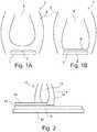
- FIG. 1Ashows a first step of a first embodiment of the method according to the invention.
- a substrate 1is provided with an emissive photoluminescent layer 2.
- a vapor plume 3 with particles of a target materialis generated with a physical vapor deposition method, such as a pulsed laser deposition method.
- This vapor plume 3has a core 4 and an envelope 5.
- the pressureis relative high, such that the kinetic energy of the particles within the plume 3 is reduced and the particles have a 'soft landing' on the surface of the emissive photoluminescent layer and form a first layer of target material 6.
- the pressureis reduced, such that the particles within the plume 3 keep their kinetic energy and are deposited on top of the first layer of target material 6 in the conventional way to form the second layer of target material. Because the first layer 6 is already arranged on top of the sensitive material 2, protecting this layer 2 and enabling conventional deposition of a second layer.
- FIG. 2shows a second embodiment of the method according to the invention.
- a substrate 10is provided with an emissive photoluminescent layer. Furthermore, a vapor plume 12 is generated. This vapor plume 12 has a core 13 with particles having a relative high velocity, and an envelope 14 around the core 13 with particles with a relatively low velocity.
- the plume 12is moved over the surface of the emissive photoluminescent layer 11.
- the envelope 14deposits first a first layer 15 of target material of the emissive photoluminescent layer 11.
- the trailing core 13then deposits a second layer 16 on the already deposited first layer 15.
- FIG. 3shows an embodiment 20 of an organic light emitting diode (OLED).
- This OLED 20has a substrate layer 21, like a glass layer.
- a first conductive layer 22is deposited with a conventional physical vapor deposition method on this substrate layer 21.
- an emissive electroluminescent layer 23is provided on top of the conductive layer 22.
- a second conductive layer 24, 25is arranged on top of the sensitive, emissive electroluminescent layer 23.
- the first layer 24 of transparent conductive materialis first deposited, after which the second layer 25 of transparent conductive material is deposited. Because both layers 24, 25 are subsequently deposited , a homogeneous layer is provide on the emissive electroluminescent layer 23.
- both conductive layers 22 and 24, 25When a voltage is applied to the two conductive layers 22 and 24, 25 the emissive electroluminescent layer 23 will emit light.
- both conductive layerscan be made transparent using for example indium tin oxide , a fully transparent OLED is obtained.
Landscapes
- Chemical & Material Sciences (AREA)
- Engineering & Computer Science (AREA)
- Organic Chemistry (AREA)
- Materials Engineering (AREA)
- Mechanical Engineering (AREA)
- Metallurgy (AREA)
- Chemical Kinetics & Catalysis (AREA)
- Physics & Mathematics (AREA)
- Optics & Photonics (AREA)
- Health & Medical Sciences (AREA)
- Toxicology (AREA)
- Manufacturing & Machinery (AREA)
- Electroluminescent Light Sources (AREA)
- Physical Vapour Deposition (AREA)
Description
- The invention relates to a method for depositing a target material onto a sensitive material.
- Depositing methods, and in particular physical vapor deposition methods, use a plume of vapor with particles, which are bombarded onto a substrate material. This plume of vapor is generated by exciting a target material, such that particles are freed from the target material. Due to the excitement, the particles gain kinetic energy, which moves the particles to the substrate and which energy is used for the particles to adhere to the substrate or even penetrate the substrate material. Depending on the substrate material and the obtained kinetic energy, the particles will penetrate to a certain depth of the substrate material and/or damage the material due to the bombardment. In the field of organic light emitting diodes (OLEDs) efforts are made to provide transparent OLEDs. An OLED has typically a layered structure of a glass or transparent plastic layer, a first conducting layer, an emissive electroluminescent layer and a second conducting layer. By providing a voltage to the first and second conducting layer, the emissive electroluminescent layer is powered, such that it will emit light.
- A transparent emissive electroluminescent layer is known, as well as transparent conducting layers. Typically a indium tin oxide layer is used for a transparent conducting layer, which is arranged on a substrate with a physical vapor deposition method. See for example "Chung C H et al: "Radio frequency magnetron sputter deposited indium tin oxide for use as a cathode in transparent organic light-emitting diode" Thin Solid Films, vol. 491, n°1-2, pages 294-297. However, if a known physical vapor deposition method is used to deposit indium tin oxide, or a similar transparent conducting oxide, to the transparent emissive electroluminescent layer, the impact of the particles damages the emissive electroluminescent layer to the extent, that it no longer emits light when being powered, or its efficiency is strongly reduced due to a leakage current or short circuiting.
- It is known to use a silver deposition on the emissive electroluminescent layer. Silver has the advantage that it can be deposited under such conditions, that it will not damage the emissive electroluminescent layer. However, the transparency of a silver layer is restricted. Typically, an OLED with a silver layer as one of the conductive layers can have a transparency of up to 40%.
- Another disadvantage of the known methods, in particular laser deposition methods, is that they use ultraviolet light. Ultraviolet light damages the materials, which are typically used for OLED production. UV light in combination with the bombardment of particles is typically damaging for organic materials used for OLED production.
- A possibility would be to arrange a protective layer of another material, which blocks ultraviolet light. However, such layers are often not transparent and in the case when an electrically conducting layer is to be arranged, the protective layer will isolate the electrically conducting layer from the emissive electroluminescent layer.
- It is therefore an object of the invention to provide a method, in which the above mentioned disadvantages are reduced or even prevented.
- This object is achieved with a method according to the preamble, which method comprises the steps of:
- providing a substrate with an emissive electroluminescent layer;
- creating a vapor plume of target material by a physical vapor deposition method;
- depositing a first layer of target material on the sensitive material, while maintaining the maximum particle velocity of the deposited particles below a preset value; and
- depositing a second layer of target material on the first layer of target material, while the maximum particle velocity of the deposited particles is above the preset value.
- With the method according to the invention, a first layer of target material is arranged on the emissive electroluminescent layer without destroying the material. This is achieved by ensuring that the maximum particle velocity is maintained below a preset value. When the particle velocity, and thus the kinetic energy, of the particles is below a preset value, the particles will attach to the sensitive material, but will not penetrate and/or damage the sensitive material, which could negatively affect the sensitive material.
- In case an UV laser is used for creating the vapor plume, the first layer could also provide an UV protection for the sensitive material, such that a higher UV intensity can be used during deposition of the second layer. In an embodiment of the invention the distance between the target material and the substrate is increased during depositing the first layer and said distance is decreased during depositing the second layer. This results in a lower maximum particle velocity on impact of the particles on the substrate and also a lower UV intensity on the substrate when the first layer is deposited.
- Then the second layer is deposited on the first layer. The already deposited layer provides a protective layer for the sensitive material, so the target material particles for the second layer can have a higher velocity during depositing than the target material particles used for the first layer.
- With the method according to the invention, it is, because of the first layer, thus possible to deposit the target material in a conventional way on an emissive electroluminescent material which would otherwise damage this sensitive material.
- The preset value will have to be determined by experiment as the preset value will at least depend on the material of the target material, the physical vapor deposition method, the chosen deposition parameters and the emissive photoluminescent material.
- In a preferred embodiment of the method according to the invention the first layer is deposited while using a first pressure regime, the second layer is deposited while using a second pressure regime and wherein the second pressure is lower than the first pressure.
- With a physical depositing method a near vacuum environment is created in which the depositing is performed. By controlling the vacuum or the pressure in this environment, the impact velocity of the particles can be controlled. When a higher pressure regime is used, the particles of the target material in the vapor plume are slowed down more, such that the impact on the substrate is less violent and the emissive photoluminescent material is no longer affected. With a higher pressure regime, the particles have a 'soft landing' on the emissive photoluminescent material.
- As soon as the first layer is deposited with the target material, the pressure regime can be lowered, such that the particles can keep their speed and impact with full energy on the first layer, without damaging the underlying emissive photoluminescent material.
- Although it would be most common to deposit the first and second layer with the same material, it will also be possible to change the target material before depositing the second layer. By using two different target materials, specific properties can be achieved for the layer deposited on the sensitive material.
- In a further preferred embodiment of the method according to the invention the vapor plume is moved over the surface of the sensitive material (as disclosed in
EP 2159300A1 ) and the vapor plume is controlled such, that the maximum velocity of the particles in the core of the plume is above the preset value and the maximum velocity of the particles around the core is below the preset value. - When a vapor plume is generated by exciting a target material with for example a laser beam, the vapor plume will have a core with a high concentration of particles having a high velocity. This core is surrounded with an envelope with a lower concentration of particles. The particles in the envelope will have a lower velocity.
- By moving the vapor plume over the surface of the emissive photoluminescent material, the envelope with lower concentration of particles will deposit first on the emissive photoluminescent material. This provides the emissive photoluminescent material with the first layer of target material along the path of the plume. While the plume moves further, the core will pass over the material already deposited by the envelope of the plume. The particles within the core of the plume will then deposit the second layer of target material.
- Preferably, the movement of the vapor plume starts outside of the surface of the emissive photoluminescent material. This ensures, that both the first layer and second layer of target material extend to the full surface of the emissive photoluminescent material.
- When the vapor plume is moved over the surface of the emissive photoluminescent material it is necessary that the maximum velocity of the particles in the core of the plume is above the preset value and the maximum velocity of the particles around the core is below the preset value. Due to the way a vapor plume is generated, there is already a difference in particle velocity of the particles in the core and the particles enveloping the core. Choosing a suitable pressure regime, will ensure, that the maximum particle velocity of the particles in the envelope is below the preset value, while the maximum velocity in the core is higher.
- In yet another embodiment of the method according to the invention the physical vapor deposition method is a pulsed laser deposition.
- In a further embodiment of the method according to the invention, the combined first and second layer is a transparent conducting oxide, in particular indium tin oxide.
- A transparent conducting oxide is a typical material, which could not be arranged on a sensitive material, like an emissive electroluminescent layer, without the method according to the invention.
- The invention also relates to an intermediate product manufactured with the method according to the invention, wherein the product comprises:
- a substrate with an emissive electroluminescent layer;
- a first layer of target material deposited on the emissive photoluminescent layer wherein the deposited particles have marginally penetrated and/or damaged the emissive photoluminescent layer.
- With the intermediate product of the invention, a first layer of target material is arranged on the substrate with an emissive photoluminescent layer. The deposited particles have marginally penetrated the emissive photoluminescent layer such that the emissive photoluminescent layer is not affected. The particles are arranged on the emissive photoluminescent material and have not, or only slightly, penetrated this sensitive material.
- The invention also relates to an organic light emitting diode comprising:
- a substrate layer;
- a first electric conducting layer arranged on the substrate layer;
- an emissive electroluminescent layer arranged on the first electric conducting layer; and
- a second electric conducting layer arranged on the emissive electroluminescent layer;
- These and other features of the invention will be elucidated in conjunction with the accompanying drawings.
Figure 1A and 1B show two steps of a first embodiment according to the invention.Figure 2 shows a second embodiment of the method according to the invention.Figure 3 shows a cross sectional view of an embodiment of the organic light emitting diode according to the invention.Figure 1A shows a first step of a first embodiment of the method according to the invention. Asubstrate 1 is provided with anemissive photoluminescent layer 2. Avapor plume 3 with particles of a target material is generated with a physical vapor deposition method, such as a pulsed laser deposition method. Thisvapor plume 3 has acore 4 and anenvelope 5.- By controlling the pressure regime in which the
vapor plume 3 is generated, the reach of theplume 3 and the impact of the particles within theplume 3 can be controlled. In the step shown infigure 1A , the pressure is relative high, such that the kinetic energy of the particles within theplume 3 is reduced and the particles have a 'soft landing' on the surface of the emissive photoluminescent layer and form a first layer oftarget material 6. - In the step shown in
figure 1B , the pressure is reduced, such that the particles within theplume 3 keep their kinetic energy and are deposited on top of the first layer oftarget material 6 in the conventional way to form the second layer of target material. Because thefirst layer 6 is already arranged on top of thesensitive material 2, protecting thislayer 2 and enabling conventional deposition of a second layer. Figure 2 shows a second embodiment of the method according to the invention. Asubstrate 10 is provided with an emissive photoluminescent layer. Furthermore, avapor plume 12 is generated. Thisvapor plume 12 has a core 13 with particles having a relative high velocity, and anenvelope 14 around thecore 13 with particles with a relatively low velocity.- The
plume 12 is moved over the surface of theemissive photoluminescent layer 11. Theenvelope 14 deposits first afirst layer 15 of target material of theemissive photoluminescent layer 11. The trailingcore 13 then deposits asecond layer 16 on the already depositedfirst layer 15. As thefirst layer 15 andsecond layer 16 are deposited with the same target material particles, a virtually homogeneous layer of target material on top of theemissive photoluminescent layer 11 is created. Figure 3 shows anembodiment 20 of an organic light emitting diode (OLED). ThisOLED 20 has asubstrate layer 21, like a glass layer. A firstconductive layer 22 is deposited with a conventional physical vapor deposition method on thissubstrate layer 21. Then anemissive electroluminescent layer 23 is provided on top of theconductive layer 22.- With the method according to the invention a second
conductive layer emissive electroluminescent layer 23. Thefirst layer 24 of transparent conductive material is first deposited, after which thesecond layer 25 of transparent conductive material is deposited. Because bothlayers emissive electroluminescent layer 23. - When a voltage is applied to the two
conductive layers emissive electroluminescent layer 23 will emit light. As both conductive layers can be made transparent using for example indium tin oxide , a fully transparent OLED is obtained.
Claims (9)
- Method for depositing a target material onto a sensitive material, which method comprises the steps of:- providing a substrate (1; 10) with an emissive electroluminescent layer (2; 11);- creating a vapor plume (3; 12) of target material by a physical vapor deposition method;- depositing a first layer (6; 15) of target material on the emissive electroluminescent layer (2; 11), while maintaining the maximum particle velocity of the deposited particles below a preset value, which preset value is chosen such to prevent particles from penetrating of and/or damaging the emissive electroluminescent (2; 11) layer during deposition; and- depositing a second layer (16) of target material on the first layer (6; 15) of target material, while the maximum particle velocity of the deposited particles is above the preset value.
- Method according to claim 1, wherein the first layer (6; 15) is deposited while using a first pressure regime, the second layer is deposited while using a second pressure regime and wherein the second pressure is lower than the first pressure.
- Method according to claim 1, wherein the vapor plume (12) is moved over the surface of the emissive electroluminescent layer and the vapor plume (12) is controlled such, that the maximum velocity of the particles in the core of the plume (13) is above the preset value and the maximum velocity of the particles around the core (13) is below the preset value.
- Method according to claim 3, wherein the movement of the vapor plume (3; 12) starts outside of the surface of the emissive electroluminescent layer (2; 11).
- Method according to claim 1, wherein the distance between the target material and the substrate is increased during depositing the first layer (6) and said distance is decreased during depositing the second layer.
- Method according to any of the preceding claims, wherein the physical vapor deposition method is a pulsed laser deposition.
- Method according to any of the preceding claims, wherein the combined first (6; 15) and second layer (16) is a transparent conducting oxide, in particular indium tin oxide.
- Intermediate product manufactured with the method according to any of the preceding claims, wherein the product comprises:- a substrate with an emissive electroluminescent layer;- a first layer of target material deposited on the emissive electroluminescent layer, wherein the deposited particles have marginally penetrated the emissive electroluminescent layer.
- Organic light emitting diode (20) comprising:- a substrate (21);- a first electric conducting layer (22) arranged on the substrate;- an emissive electroluminescent layer (23) arranged on the first electric conducting layer (22); and- a second electric conducting layer (24, 25) arranged on the emissive electroluminescent layer (23);characterized in that the second electric conducting layer (24, 25) is arranged using the method according to any of the claims 1 - 7.
Priority Applications (7)
| Application Number | Priority Date | Filing Date | Title |
|---|---|---|---|
| EP12188835.8AEP2722412B1 (en) | 2012-10-17 | 2012-10-17 | Method for depositing a target material onto a sensitive material |
| JP2015537210AJP6564326B2 (en) | 2012-10-17 | 2013-10-14 | Method of depositing target material on organic electronic functional material |
| CN201380060227.9ACN104812932B (en) | 2012-10-17 | 2013-10-14 | Method for depositing target material on electro-organic functional material |
| EP13774699.6AEP2909356A1 (en) | 2012-10-17 | 2013-10-14 | Method for depositing a target material onto a organic electrically functional material |
| US14/434,938US10128467B2 (en) | 2012-10-17 | 2013-10-14 | Method for depositing a target material onto a organic electrically functional material |
| KR1020157012537AKR102203556B1 (en) | 2012-10-17 | 2013-10-14 | Method for depositing a target material onto a organic electrically functional material |
| PCT/EP2013/071429WO2014060356A1 (en) | 2012-10-17 | 2013-10-14 | Method for depositing a target material onto a organic electrically functional material |
Applications Claiming Priority (1)
| Application Number | Priority Date | Filing Date | Title |
|---|---|---|---|
| EP12188835.8AEP2722412B1 (en) | 2012-10-17 | 2012-10-17 | Method for depositing a target material onto a sensitive material |
Publications (2)
| Publication Number | Publication Date |
|---|---|
| EP2722412A1 EP2722412A1 (en) | 2014-04-23 |
| EP2722412B1true EP2722412B1 (en) | 2018-04-25 |
Family
ID=47046419
Family Applications (2)
| Application Number | Title | Priority Date | Filing Date |
|---|---|---|---|
| EP12188835.8AActiveEP2722412B1 (en) | 2012-10-17 | 2012-10-17 | Method for depositing a target material onto a sensitive material |
| EP13774699.6AWithdrawnEP2909356A1 (en) | 2012-10-17 | 2013-10-14 | Method for depositing a target material onto a organic electrically functional material |
Family Applications After (1)
| Application Number | Title | Priority Date | Filing Date |
|---|---|---|---|
| EP13774699.6AWithdrawnEP2909356A1 (en) | 2012-10-17 | 2013-10-14 | Method for depositing a target material onto a organic electrically functional material |
Country Status (6)
| Country | Link |
|---|---|
| US (1) | US10128467B2 (en) |
| EP (2) | EP2722412B1 (en) |
| JP (1) | JP6564326B2 (en) |
| KR (1) | KR102203556B1 (en) |
| CN (1) | CN104812932B (en) |
| WO (1) | WO2014060356A1 (en) |
Families Citing this family (4)
| Publication number | Priority date | Publication date | Assignee | Title |
|---|---|---|---|---|
| US11224511B2 (en) | 2017-04-18 | 2022-01-18 | Edwards Lifesciences Corporation | Heart valve sealing devices and delivery devices therefor |
| CN107482130B (en)* | 2017-08-02 | 2020-05-26 | 京东方科技集团股份有限公司 | Organic light-emitting panel, method for making the same, and organic light-emitting device |
| EP3587620A1 (en)* | 2018-06-28 | 2020-01-01 | Solmates B.V. | Device for pulsed laser deposition and a substrate with a substrate surface for reduction of particles on the substrate |
| CN115275078A (en)* | 2022-07-28 | 2022-11-01 | 昆山梦显电子科技有限公司 | A kind of transparent cathode and its preparation method and OLED |
Family Cites Families (9)
| Publication number | Priority date | Publication date | Assignee | Title |
|---|---|---|---|---|
| JP3704258B2 (en)* | 1998-09-10 | 2005-10-12 | 松下電器産業株式会社 | Thin film formation method |
| JP4449116B2 (en)* | 1999-09-20 | 2010-04-14 | ソニー株式会社 | ORGANIC ELECTROLUMINESCENCE ELEMENT, MANUFACTURING METHOD THEREOF, AND DISPLAY DEVICE |
| US6645843B2 (en)* | 2001-01-19 | 2003-11-11 | The United States Of America As Represented By The Secretary Of The Navy | Pulsed laser deposition of transparent conducting thin films on flexible substrates |
| US8080935B2 (en)* | 2005-09-29 | 2011-12-20 | Panasonic Corporation | Organic EL display and method for manufacturing same |
| US20110049715A1 (en)* | 2007-12-19 | 2011-03-03 | Carlo Taliani | Method for depositing metal oxide films |
| GB0803702D0 (en)* | 2008-02-28 | 2008-04-09 | Isis Innovation | Transparent conducting oxides |
| JP2011524463A (en)* | 2008-05-06 | 2011-09-01 | エージェンシー フォー サイエンス,テクノロジー アンド リサーチ | Conductive structure for light transmissive devices |
| SI2159300T1 (en) | 2008-08-25 | 2012-05-31 | Solmates Bv | Method for depositing a material |
| JP2010287383A (en)* | 2009-06-10 | 2010-12-24 | Panasonic Corp | Method for manufacturing organic electroluminescent device |
- 2012
- 2012-10-17EPEP12188835.8Apatent/EP2722412B1/enactiveActive
- 2013
- 2013-10-14KRKR1020157012537Apatent/KR102203556B1/enactiveActive
- 2013-10-14CNCN201380060227.9Apatent/CN104812932B/enactiveActive
- 2013-10-14WOPCT/EP2013/071429patent/WO2014060356A1/enactiveApplication Filing
- 2013-10-14USUS14/434,938patent/US10128467B2/enactiveActive
- 2013-10-14JPJP2015537210Apatent/JP6564326B2/enactiveActive
- 2013-10-14EPEP13774699.6Apatent/EP2909356A1/ennot_activeWithdrawn
Non-Patent Citations (1)
| Title |
|---|
| None* |
Also Published As
| Publication number | Publication date |
|---|---|
| CN104812932A (en) | 2015-07-29 |
| JP6564326B2 (en) | 2019-08-21 |
| KR20150065897A (en) | 2015-06-15 |
| KR102203556B1 (en) | 2021-01-15 |
| JP2015533390A (en) | 2015-11-24 |
| US20150255757A1 (en) | 2015-09-10 |
| WO2014060356A1 (en) | 2014-04-24 |
| EP2909356A1 (en) | 2015-08-26 |
| US10128467B2 (en) | 2018-11-13 |
| EP2722412A1 (en) | 2014-04-23 |
| CN104812932B (en) | 2017-10-24 |
Similar Documents
| Publication | Publication Date | Title |
|---|---|---|
| EP2722412B1 (en) | Method for depositing a target material onto a sensitive material | |
| JP6192762B2 (en) | Electroluminescent device | |
| JP2012519955A (en) | OLEDs connected in series | |
| CN101395733A (en) | Electroluminescent arrangement | |
| KR20150045329A (en) | An organic light emtting device | |
| KR20140096382A (en) | Method for producing an optoelectronic component, and optoelectronic component | |
| JP6142363B2 (en) | Method for manufacturing organic electroluminescent device | |
| KR20140108110A (en) | Method of manufacturing organic el element | |
| CN106029942A (en) | Device for depositing material by pulsed laser deposition and method for depositing material using the device | |
| KR101731274B1 (en) | Organic electroluminescent devices | |
| CN103730595A (en) | Organic light-emitting device and preparation method thereof | |
| CN103855315A (en) | Organic light-emitting device and preparation method thereof | |
| WO2015129892A1 (en) | Organic electroluminescent element manufacturing method and manufacturing device | |
| CN103378302A (en) | Organic light-emitting device and encapsulating method thereof | |
| WO2020199828A1 (en) | Method for manufacturing cathode of display panel, display panel, and display apparatus | |
| CN104078590A (en) | Organic light-emitting diode and preparation method thereof | |
| US20080264680A1 (en) | Voltage-Operated Layer Arrangement | |
| Wakeham et al. | Laser annealing of thin film electroluminescent devices deposited at a high rate using high target utilization sputtering | |
| CN103594650A (en) | Organic electroluminescent device and preparation method thereof | |
| CN103378303A (en) | Organic light-emitting device and encapsulating method thereof | |
| JP2018147813A (en) | Display device manufacturing method and display device | |
| JP4925903B2 (en) | Organic EL device, organic EL device manufacturing method | |
| JP2008243874A (en) | Organic EL device, organic EL device manufacturing method | |
| WO2014020789A1 (en) | Organic electroluminescent element and method for manufacturing organic electroluminescent element | |
| CN103378304A (en) | Organic light-emitting device and encapsulating method thereof |
Legal Events
| Date | Code | Title | Description |
|---|---|---|---|
| PUAI | Public reference made under article 153(3) epc to a published international application that has entered the european phase | Free format text:ORIGINAL CODE: 0009012 | |
| AK | Designated contracting states | Kind code of ref document:A1 Designated state(s):AL AT BE BG CH CY CZ DE DK EE ES FI FR GB GR HR HU IE IS IT LI LT LU LV MC MK MT NL NO PL PT RO RS SE SI SK SM TR | |
| AX | Request for extension of the european patent | Extension state:BA ME | |
| 17P | Request for examination filed | Effective date:20141016 | |
| RBV | Designated contracting states (corrected) | Designated state(s):AL AT BE BG CH CY CZ DE DK EE ES FI FR GB GR HR HU IE IS IT LI LT LU LV MC MK MT NL NO PL PT RO RS SE SI SK SM TR | |
| 17Q | First examination report despatched | Effective date:20161117 | |
| GRAP | Despatch of communication of intention to grant a patent | Free format text:ORIGINAL CODE: EPIDOSNIGR1 | |
| RAP1 | Party data changed (applicant data changed or rights of an application transferred) | Owner name:SOLMATES B.V. | |
| INTG | Intention to grant announced | Effective date:20171207 | |
| GRAA | (expected) grant | Free format text:ORIGINAL CODE: 0009210 | |
| GRAS | Grant fee paid | Free format text:ORIGINAL CODE: EPIDOSNIGR3 | |
| AK | Designated contracting states | Kind code of ref document:B1 Designated state(s):AL AT BE BG CH CY CZ DE DK EE ES FI FR GB GR HR HU IE IS IT LI LT LU LV MC MK MT NL NO PL PT RO RS SE SI SK SM TR | |
| REG | Reference to a national code | Ref country code:GB Ref legal event code:FG4D | |
| REG | Reference to a national code | Ref country code:CH Ref legal event code:EP | |
| REG | Reference to a national code | Ref country code:AT Ref legal event code:REF Ref document number:993008 Country of ref document:AT Kind code of ref document:T Effective date:20180515 | |
| REG | Reference to a national code | Ref country code:IE Ref legal event code:FG4D | |
| REG | Reference to a national code | Ref country code:DE Ref legal event code:R096 Ref document number:602012045558 Country of ref document:DE | |
| REG | Reference to a national code | Ref country code:NL Ref legal event code:FP | |
| REG | Reference to a national code | Ref country code:LT Ref legal event code:MG4D | |
| REG | Reference to a national code | Ref country code:FR Ref legal event code:PLFP Year of fee payment:7 | |
| PG25 | Lapsed in a contracting state [announced via postgrant information from national office to epo] | Ref country code:ES Free format text:LAPSE BECAUSE OF FAILURE TO SUBMIT A TRANSLATION OF THE DESCRIPTION OR TO PAY THE FEE WITHIN THE PRESCRIBED TIME-LIMIT Effective date:20180425 Ref country code:PL Free format text:LAPSE BECAUSE OF FAILURE TO SUBMIT A TRANSLATION OF THE DESCRIPTION OR TO PAY THE FEE WITHIN THE PRESCRIBED TIME-LIMIT Effective date:20180425 Ref country code:BG Free format text:LAPSE BECAUSE OF FAILURE TO SUBMIT A TRANSLATION OF THE DESCRIPTION OR TO PAY THE FEE WITHIN THE PRESCRIBED TIME-LIMIT Effective date:20180725 Ref country code:LT Free format text:LAPSE BECAUSE OF FAILURE TO SUBMIT A TRANSLATION OF THE DESCRIPTION OR TO PAY THE FEE WITHIN THE PRESCRIBED TIME-LIMIT Effective date:20180425 Ref country code:SE Free format text:LAPSE BECAUSE OF FAILURE TO SUBMIT A TRANSLATION OF THE DESCRIPTION OR TO PAY THE FEE WITHIN THE PRESCRIBED TIME-LIMIT Effective date:20180425 Ref country code:NO Free format text:LAPSE BECAUSE OF FAILURE TO SUBMIT A TRANSLATION OF THE DESCRIPTION OR TO PAY THE FEE WITHIN THE PRESCRIBED TIME-LIMIT Effective date:20180725 | |
| PG25 | Lapsed in a contracting state [announced via postgrant information from national office to epo] | Ref country code:GR Free format text:LAPSE BECAUSE OF FAILURE TO SUBMIT A TRANSLATION OF THE DESCRIPTION OR TO PAY THE FEE WITHIN THE PRESCRIBED TIME-LIMIT Effective date:20180726 Ref country code:RS Free format text:LAPSE BECAUSE OF FAILURE TO SUBMIT A TRANSLATION OF THE DESCRIPTION OR TO PAY THE FEE WITHIN THE PRESCRIBED TIME-LIMIT Effective date:20180425 Ref country code:HR Free format text:LAPSE BECAUSE OF FAILURE TO SUBMIT A TRANSLATION OF THE DESCRIPTION OR TO PAY THE FEE WITHIN THE PRESCRIBED TIME-LIMIT Effective date:20180425 Ref country code:LV Free format text:LAPSE BECAUSE OF FAILURE TO SUBMIT A TRANSLATION OF THE DESCRIPTION OR TO PAY THE FEE WITHIN THE PRESCRIBED TIME-LIMIT Effective date:20180425 | |
| REG | Reference to a national code | Ref country code:AT Ref legal event code:MK05 Ref document number:993008 Country of ref document:AT Kind code of ref document:T Effective date:20180425 | |
| PG25 | Lapsed in a contracting state [announced via postgrant information from national office to epo] | Ref country code:PT Free format text:LAPSE BECAUSE OF FAILURE TO SUBMIT A TRANSLATION OF THE DESCRIPTION OR TO PAY THE FEE WITHIN THE PRESCRIBED TIME-LIMIT Effective date:20180827 | |
| REG | Reference to a national code | Ref country code:DE Ref legal event code:R097 Ref document number:602012045558 Country of ref document:DE | |
| PG25 | Lapsed in a contracting state [announced via postgrant information from national office to epo] | Ref country code:RO Free format text:LAPSE BECAUSE OF FAILURE TO SUBMIT A TRANSLATION OF THE DESCRIPTION OR TO PAY THE FEE WITHIN THE PRESCRIBED TIME-LIMIT Effective date:20180425 Ref country code:CZ Free format text:LAPSE BECAUSE OF FAILURE TO SUBMIT A TRANSLATION OF THE DESCRIPTION OR TO PAY THE FEE WITHIN THE PRESCRIBED TIME-LIMIT Effective date:20180425 Ref country code:SK Free format text:LAPSE BECAUSE OF FAILURE TO SUBMIT A TRANSLATION OF THE DESCRIPTION OR TO PAY THE FEE WITHIN THE PRESCRIBED TIME-LIMIT Effective date:20180425 Ref country code:AT Free format text:LAPSE BECAUSE OF FAILURE TO SUBMIT A TRANSLATION OF THE DESCRIPTION OR TO PAY THE FEE WITHIN THE PRESCRIBED TIME-LIMIT Effective date:20180425 Ref country code:EE Free format text:LAPSE BECAUSE OF FAILURE TO SUBMIT A TRANSLATION OF THE DESCRIPTION OR TO PAY THE FEE WITHIN THE PRESCRIBED TIME-LIMIT Effective date:20180425 Ref country code:DK Free format text:LAPSE BECAUSE OF FAILURE TO SUBMIT A TRANSLATION OF THE DESCRIPTION OR TO PAY THE FEE WITHIN THE PRESCRIBED TIME-LIMIT Effective date:20180425 | |
| PG25 | Lapsed in a contracting state [announced via postgrant information from national office to epo] | Ref country code:SM Free format text:LAPSE BECAUSE OF FAILURE TO SUBMIT A TRANSLATION OF THE DESCRIPTION OR TO PAY THE FEE WITHIN THE PRESCRIBED TIME-LIMIT Effective date:20180425 | |
| PLBE | No opposition filed within time limit | Free format text:ORIGINAL CODE: 0009261 | |
| STAA | Information on the status of an ep patent application or granted ep patent | Free format text:STATUS: NO OPPOSITION FILED WITHIN TIME LIMIT | |
| 26N | No opposition filed | Effective date:20190128 | |
| PG25 | Lapsed in a contracting state [announced via postgrant information from national office to epo] | Ref country code:SI Free format text:LAPSE BECAUSE OF FAILURE TO SUBMIT A TRANSLATION OF THE DESCRIPTION OR TO PAY THE FEE WITHIN THE PRESCRIBED TIME-LIMIT Effective date:20180425 | |
| GBPC | Gb: european patent ceased through non-payment of renewal fee | Effective date:20181017 | |
| PG25 | Lapsed in a contracting state [announced via postgrant information from national office to epo] | Ref country code:LU Free format text:LAPSE BECAUSE OF NON-PAYMENT OF DUE FEES Effective date:20181017 Ref country code:MC Free format text:LAPSE BECAUSE OF FAILURE TO SUBMIT A TRANSLATION OF THE DESCRIPTION OR TO PAY THE FEE WITHIN THE PRESCRIBED TIME-LIMIT Effective date:20180425 | |
| PG25 | Lapsed in a contracting state [announced via postgrant information from national office to epo] | Ref country code:GB Free format text:LAPSE BECAUSE OF NON-PAYMENT OF DUE FEES Effective date:20181017 | |
| PG25 | Lapsed in a contracting state [announced via postgrant information from national office to epo] | Ref country code:AL Free format text:LAPSE BECAUSE OF FAILURE TO SUBMIT A TRANSLATION OF THE DESCRIPTION OR TO PAY THE FEE WITHIN THE PRESCRIBED TIME-LIMIT Effective date:20180425 | |
| PG25 | Lapsed in a contracting state [announced via postgrant information from national office to epo] | Ref country code:MT Free format text:LAPSE BECAUSE OF NON-PAYMENT OF DUE FEES Effective date:20181017 | |
| PG25 | Lapsed in a contracting state [announced via postgrant information from national office to epo] | Ref country code:TR Free format text:LAPSE BECAUSE OF FAILURE TO SUBMIT A TRANSLATION OF THE DESCRIPTION OR TO PAY THE FEE WITHIN THE PRESCRIBED TIME-LIMIT Effective date:20180425 | |
| PG25 | Lapsed in a contracting state [announced via postgrant information from national office to epo] | Ref country code:HU Free format text:LAPSE BECAUSE OF FAILURE TO SUBMIT A TRANSLATION OF THE DESCRIPTION OR TO PAY THE FEE WITHIN THE PRESCRIBED TIME-LIMIT; INVALID AB INITIO Effective date:20121017 Ref country code:MK Free format text:LAPSE BECAUSE OF NON-PAYMENT OF DUE FEES Effective date:20180425 Ref country code:CY Free format text:LAPSE BECAUSE OF FAILURE TO SUBMIT A TRANSLATION OF THE DESCRIPTION OR TO PAY THE FEE WITHIN THE PRESCRIBED TIME-LIMIT Effective date:20180425 | |
| PG25 | Lapsed in a contracting state [announced via postgrant information from national office to epo] | Ref country code:IS Free format text:LAPSE BECAUSE OF FAILURE TO SUBMIT A TRANSLATION OF THE DESCRIPTION OR TO PAY THE FEE WITHIN THE PRESCRIBED TIME-LIMIT Effective date:20180825 | |
| PGFP | Annual fee paid to national office [announced via postgrant information from national office to epo] | Ref country code:NL Payment date:20221026 Year of fee payment:11 | |
| REG | Reference to a national code | Ref country code:DE Ref legal event code:R081 Ref document number:602012045558 Country of ref document:DE Owner name:LAM RESEARCH CORPORATION (N.D.GES.D.STAATES DE, US Free format text:FORMER OWNER: SOLMATES B.V., ENSCHEDE, NL | |
| PGFP | Annual fee paid to national office [announced via postgrant information from national office to epo] | Ref country code:IE Payment date:20221027 Year of fee payment:11 Ref country code:FI Payment date:20221027 Year of fee payment:11 | |
| PGFP | Annual fee paid to national office [announced via postgrant information from national office to epo] | Ref country code:CH Payment date:20221116 Year of fee payment:11 | |
| REG | Reference to a national code | Ref country code:BE Ref legal event code:PD Owner name:LAM RESEARCH CORPORATION; US Free format text:DETAILS ASSIGNMENT: CHANGE OF OWNER(S), ASSIGNMENT; FORMER OWNER NAME: SOLMATES B.V. Effective date:20230929 | |
| P01 | Opt-out of the competence of the unified patent court (upc) registered | Effective date:20231021 | |
| REG | Reference to a national code | Ref country code:CH Ref legal event code:PL | |
| REG | Reference to a national code | Ref country code:NL Ref legal event code:MM Effective date:20231101 | |
| PG25 | Lapsed in a contracting state [announced via postgrant information from national office to epo] | Ref country code:NL Free format text:LAPSE BECAUSE OF NON-PAYMENT OF DUE FEES Effective date:20231101 Ref country code:CH Free format text:LAPSE BECAUSE OF NON-PAYMENT OF DUE FEES Effective date:20231031 | |
| PG25 | Lapsed in a contracting state [announced via postgrant information from national office to epo] | Ref country code:NL Free format text:LAPSE BECAUSE OF NON-PAYMENT OF DUE FEES Effective date:20231101 Ref country code:FI Free format text:LAPSE BECAUSE OF NON-PAYMENT OF DUE FEES Effective date:20231017 Ref country code:CH Free format text:LAPSE BECAUSE OF NON-PAYMENT OF DUE FEES Effective date:20231031 | |
| PG25 | Lapsed in a contracting state [announced via postgrant information from national office to epo] | Ref country code:IE Free format text:LAPSE BECAUSE OF NON-PAYMENT OF DUE FEES Effective date:20231017 | |
| PG25 | Lapsed in a contracting state [announced via postgrant information from national office to epo] | Ref country code:IE Free format text:LAPSE BECAUSE OF NON-PAYMENT OF DUE FEES Effective date:20231017 | |
| PGFP | Annual fee paid to national office [announced via postgrant information from national office to epo] | Ref country code:DE Payment date:20241029 Year of fee payment:13 | |
| PGFP | Annual fee paid to national office [announced via postgrant information from national office to epo] | Ref country code:BE Payment date:20241028 Year of fee payment:13 | |
| PGFP | Annual fee paid to national office [announced via postgrant information from national office to epo] | Ref country code:FR Payment date:20241025 Year of fee payment:13 | |
| PGFP | Annual fee paid to national office [announced via postgrant information from national office to epo] | Ref country code:IT Payment date:20241021 Year of fee payment:13 |