EP2719167B1 - Low power and small form factor infrared imaging - Google Patents
Low power and small form factor infrared imagingDownload PDFInfo
- Publication number
- EP2719167B1 EP2719167B1EP12737632.5AEP12737632AEP2719167B1EP 2719167 B1EP2719167 B1EP 2719167B1EP 12737632 AEP12737632 AEP 12737632AEP 2719167 B1EP2719167 B1EP 2719167B1
- Authority
- EP
- European Patent Office
- Prior art keywords
- approximately
- infrared sensors
- infrared
- image frames
- fpa
- Prior art date
- Legal status (The legal status is an assumption and is not a legal conclusion. Google has not performed a legal analysis and makes no representation as to the accuracy of the status listed.)
- Active
Links
Images


Classifications
- H—ELECTRICITY
- H04—ELECTRIC COMMUNICATION TECHNIQUE
- H04N—PICTORIAL COMMUNICATION, e.g. TELEVISION
- H04N25/00—Circuitry of solid-state image sensors [SSIS]; Control thereof
- H04N25/70—SSIS architectures; Circuits associated therewith
- H04N25/709—Circuitry for control of the power supply
- H—ELECTRICITY
- H04—ELECTRIC COMMUNICATION TECHNIQUE
- H04N—PICTORIAL COMMUNICATION, e.g. TELEVISION
- H04N23/00—Cameras or camera modules comprising electronic image sensors; Control thereof
- H04N23/50—Constructional details
- H04N23/51—Housings
- H—ELECTRICITY
- H04—ELECTRIC COMMUNICATION TECHNIQUE
- H04N—PICTORIAL COMMUNICATION, e.g. TELEVISION
- H04N23/00—Cameras or camera modules comprising electronic image sensors; Control thereof
- H04N23/57—Mechanical or electrical details of cameras or camera modules specially adapted for being embedded in other devices
- H—ELECTRICITY
- H04—ELECTRIC COMMUNICATION TECHNIQUE
- H04N—PICTORIAL COMMUNICATION, e.g. TELEVISION
- H04N25/00—Circuitry of solid-state image sensors [SSIS]; Control thereof
- H04N25/20—Circuitry of solid-state image sensors [SSIS]; Control thereof for transforming only infrared radiation into image signals
- H04N25/21—Circuitry of solid-state image sensors [SSIS]; Control thereof for transforming only infrared radiation into image signals for transforming thermal infrared radiation into image signals
- H—ELECTRICITY
- H04—ELECTRIC COMMUNICATION TECHNIQUE
- H04N—PICTORIAL COMMUNICATION, e.g. TELEVISION
- H04N25/00—Circuitry of solid-state image sensors [SSIS]; Control thereof
- H04N25/60—Noise processing, e.g. detecting, correcting, reducing or removing noise
- H—ELECTRICITY
- H04—ELECTRIC COMMUNICATION TECHNIQUE
- H04N—PICTORIAL COMMUNICATION, e.g. TELEVISION
- H04N25/00—Circuitry of solid-state image sensors [SSIS]; Control thereof
- H04N25/60—Noise processing, e.g. detecting, correcting, reducing or removing noise
- H04N25/67—Noise processing, e.g. detecting, correcting, reducing or removing noise applied to fixed-pattern noise, e.g. non-uniformity of response
- H04N25/671—Noise processing, e.g. detecting, correcting, reducing or removing noise applied to fixed-pattern noise, e.g. non-uniformity of response for non-uniformity detection or correction
- H04N25/673—Noise processing, e.g. detecting, correcting, reducing or removing noise applied to fixed-pattern noise, e.g. non-uniformity of response for non-uniformity detection or correction by using reference sources
- H—ELECTRICITY
- H04—ELECTRIC COMMUNICATION TECHNIQUE
- H04N—PICTORIAL COMMUNICATION, e.g. TELEVISION
- H04N25/00—Circuitry of solid-state image sensors [SSIS]; Control thereof
- H04N25/70—SSIS architectures; Circuits associated therewith
- H04N25/76—Addressed sensors, e.g. MOS or CMOS sensors
- H04N25/78—Readout circuits for addressed sensors, e.g. output amplifiers or A/D converters
- H—ELECTRICITY
- H10—SEMICONDUCTOR DEVICES; ELECTRIC SOLID-STATE DEVICES NOT OTHERWISE PROVIDED FOR
- H10F—INORGANIC SEMICONDUCTOR DEVICES SENSITIVE TO INFRARED RADIATION, LIGHT, ELECTROMAGNETIC RADIATION OF SHORTER WAVELENGTH OR CORPUSCULAR RADIATION
- H10F39/00—Integrated devices, or assemblies of multiple devices, comprising at least one element covered by group H10F30/00, e.g. radiation detectors comprising photodiode arrays
- H10F39/10—Integrated devices
- H10F39/12—Image sensors
- H10F39/18—Complementary metal-oxide-semiconductor [CMOS] image sensors; Photodiode array image sensors
- H10F39/184—Infrared image sensors
- H—ELECTRICITY
- H10—SEMICONDUCTOR DEVICES; ELECTRIC SOLID-STATE DEVICES NOT OTHERWISE PROVIDED FOR
- H10F—INORGANIC SEMICONDUCTOR DEVICES SENSITIVE TO INFRARED RADIATION, LIGHT, ELECTROMAGNETIC RADIATION OF SHORTER WAVELENGTH OR CORPUSCULAR RADIATION
- H10F39/00—Integrated devices, or assemblies of multiple devices, comprising at least one element covered by group H10F30/00, e.g. radiation detectors comprising photodiode arrays
- H10F39/80—Constructional details of image sensors
- H10F39/804—Containers or encapsulations
- H—ELECTRICITY
- H04—ELECTRIC COMMUNICATION TECHNIQUE
- H04M—TELEPHONIC COMMUNICATION
- H04M1/00—Substation equipment, e.g. for use by subscribers
- H04M1/72—Mobile telephones; Cordless telephones, i.e. devices for establishing wireless links to base stations without route selection
- H04M1/725—Cordless telephones
- H—ELECTRICITY
- H04—ELECTRIC COMMUNICATION TECHNIQUE
- H04M—TELEPHONIC COMMUNICATION
- H04M2250/00—Details of telephonic subscriber devices
- H04M2250/52—Details of telephonic subscriber devices including functional features of a camera
Definitions
- One or more embodiments of the inventionrelate generally to thermal imaging devices and more particularly, for example, to the implementation and operation of such devices in a manner appropriate for low power and small form factor applications.
- Infrared imaging devicessuch as infrared cameras or other devices, are typically implemented with an array of infrared sensors.
- existing infrared sensors and related circuitryare typically sensitive to noise and other phenomena. Because of such sensitivity, infrared sensors and related circuitry are often implemented with power supply arrangements wherein multiple voltage supply paths provide different voltages to various circuit components. However, such implementations are typically complex and may be relatively inefficient.
- infrared imaging devicesmay experience significant self-heating which may cause various undesirable thermal effects. Nevertheless, conventional techniques to reduce such effects are also less than ideal and may rely on active cooling or other measures that increase the cost and complexity of infrared imaging devices.
- Document US 2002/058352 A1discloses a two-dimensional array of Lead-Salt detector elements monolithically formed and mounted on an integrated circuit that includes an integrated circuit having a passivation layer and a plurality of electrical contacts.
- the systemalso includes a delineated, sensitized Lead-Salt layer upon the passivation layer, the delineations forming a plurality of detector elements.
- the systemadditionally includes vias through the passivation layer to the electrical contacts and electrical couplers between the electrical contacts and the detector elements.
- Document US 6444983 B1discloses a common structure of a FPA comprising an array of microbolometers, a bias voltage circuit and a ROIC.
- a bias voltage of the similar system of document XP055345084is 1,6 V while the bias voltage range used by the similar system of document XP055345096 is 2-8 V.
- a systemincludes a focal plane array (FPA) comprising: an array of infrared sensors adapted to image a scene; a bias circuit adapted to provide a bias voltage to the infrared sensors, wherein the bias voltage is selected from a range of approximately 0.2 volts to approximately 0.7 volts; and a read out integrated circuit (ROIC) adapted to provide signals from the infrared sensors corresponding to captured image frames.
- FPAfocal plane array
- ROICread out integrated circuit
- a systemin another embodiment, includes a focal plane array (FPA) comprising: an array of infrared sensors adapted to image a scene, wherein a size of the array of infrared sensors is less than approximately 160 by 120; and a read out integrated circuit (ROIC) adapted to provide signals from the infrared sensors corresponding to captured image frames, wherein the ROIC is adapted to provide the captured image frames at a frame rate selected from a range of approximately 120 Hz to approximately 480 Hz.
- FPAfocal plane array
- ROICread out integrated circuit
- a methodin another embodiment, includes providing a bias voltage from a bias circuit of a focal plane array (FPA) to an array of infrared sensors of the FPA, wherein the bias voltage is selected from a range of approximately 0.2 volts to approximately 0.7 volts; imaging the scene using the infrared sensors; and providing signals from the infrared sensors corresponding to captured image frames of the scene using a read out integrated circuit (ROIC) of the FPA.
- FPAfocal plane array
- ROICread out integrated circuit
- a methodin another embodiment, includes imaging a scene using an array of infrared sensors of a focal plane array (FPA), wherein a size of the array of infrared sensors is less than approximately 160 by 120; and providing signals from the infrared sensors corresponding to captured image frames using a read out integrated circuit (ROIC) of the FPA, wherein the ROIC provides the captured image frames at a frame rate selected from a range of approximately 120 Hz to approximately 480 Hz.
- FPAfocal plane array
- ROICread out integrated circuit
- a systemin another embodiment, includes a focal plane array (FPA) comprising: a low-dropout regulator (LDO) integrated with the FPA and adapted to provide a regulated voltage in response to an external supply voltage; an array of infrared sensors adapted to image a scene; a bias circuit adapted to provide a bias voltage to the infrared sensors in response to the regulated voltage; and a read out integrated circuit (ROIC) adapted to provide signals from the infrared sensors corresponding to captured image frames.
- FPAfocal plane array
- LDOlow-dropout regulator
- ROICread out integrated circuit
- a methodin another embodiment, includes receiving an external supply voltage at a focal plane array (FPA); providing a regulated voltage in response to the external supply voltage using a low-dropout regulator (LDO) integrated with the FPA; providing a bias voltage to an array infrared sensors of the FPA in response to the regulated voltage using the bias circuit of the FPA; imaging a scene using the infrared sensors; and providing signals from the infrared sensors corresponding to captured image frames using a read out integrated circuit (ROIC) of the FPA.
- FPAfocal plane array
- LDOlow-dropout regulator
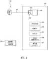
- Fig. 1illustrates an infrared imaging module 100 (e.g., an infrared camera or an infrared imaging device) configured to be implemented in a host device 102 in accordance with an embodiment of the disclosure.
- Infrared imaging module 100may be implemented, for one or more embodiments, with a small form factor and in accordance with wafer level packaging techniques or other packaging techniques.
- infrared imaging module 100may be configured to be implemented in a small portable host device 102, such as a mobile telephone, a tablet computing device, a laptop computing device, a personal digital assistant, a visible light camera, a music player, or any other appropriate mobile device.
- infrared imaging module 100may be used to provide infrared imaging features to host device 102.
- infrared imaging module 100may be configured to capture, process, and/or otherwise manage infrared images and provide such infrared images to host device 102 for use in any desired fashion (e.g., for further processing, to store in memory, to display, to use by various applications running on host device 102, to export to other devices, or other uses).
- infrared imaging module 100may be configured to operate at low voltage levels and over a wide temperature range.
- infrared imaging module 100may operate using a power supply of approximately 2.4 volts, 2.5 volts, 2.8 volts, or lower voltages, and operate over a temperature range of approximately -20 degrees C to approximately +60 degrees C (e.g., providing a suitable dynamic range and performance over an environmental temperature range of approximately 80 degrees C).
- infrared imaging module 100may experience reduced amounts of self heating in comparison with other types of infrared imaging devices. As a result, infrared imaging module 100 may be operated with reduced measures to compensate for such self heating.
- host device 102may include a socket 104, a shutter 105, motion sensors 194, a processor 195, a memory 196, a display 197, and/or other components 198.
- Socket 104may be configured to receive infrared imaging module 100 as identified by arrow 101.
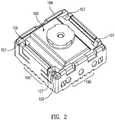
- Fig. 2illustrates infrared imaging module 100 assembled in socket 104 in accordance with an embodiment of the disclosure.
- Motion sensors 194may be implemented by one or more accelerometers, gyroscopes, or other appropriate devices that may be used to detect movement of host device 102. Motion sensors 194 may be monitored by and provide information to processing module 160 or processor 195 to detect motion. In various embodiments, motion sensors 194 may be implemented as part of host device 102 (as shown in Fig. 1 ), infrared imaging module 100, or other devices attached to or otherwise interfaced with host device 102.
- Processor 195may be implemented as any appropriate processing device (e.g., logic device, microcontroller, processor, application specific integrated circuit (ASIC), or other device) that may be used by host device 102 to execute appropriate instructions, such as software instructions provided in memory 196.
- Display 197may be used to display captured and/or processed infrared images and/or other images, data, and information.
- Other components 198may be used to implement any features of host device 102 as may be desired for various applications (e.g., clocks, temperature sensors, a visible light camera, or other components).
- a machine readable medium 193may be provided for storing non-transitory instructions for loading into memory 196 and execution by processor 195.
- infrared imaging module 100 and socket 104may be implemented for mass production to facilitate high volume applications, such as for implementation in mobile telephones or other devices (e.g., requiring small form factors).
- the combination of infrared imaging module 100 and socket 104may exhibit overall dimensions of approximately 8.5 mm by 8.5 mm by 5.9 mm while infrared imaging module 100 is installed in socket 104.
- FIG. 3illustrates an exploded view of infrared imaging module 100 juxtaposed over socket 104 in accordance with an embodiment of the disclosure.
- Infrared imaging module 100may include a lens barrel 110, a housing 120, an infrared sensor assembly 128, a circuit board 170, a base 150, and a processing module 160.
- Lens barrel 110may at least partially enclose an optical element 180 (e.g., a lens) which is partially visible in Fig. 3 through an aperture 112 in lens barrel 110.
- Lens barrel 110may include a substantially cylindrical extension 114 which may be used to interface lens barrel 110 with an aperture 122 in housing 120.
- Infrared sensor assembly 128may be implemented, for example, with a cap 130 (e.g., a lid) mounted on a substrate 140.
- Infrared sensor assembly 128may include a plurality of infrared sensors 132 (e.g., infrared detectors) implemented in an array or other fashion on substrate 140 and covered by cap 130.
- infrared sensor assembly 128may be implemented as a focal plane array (FPA).
- FPAfocal plane array
- Such a focal plane arraymay be implemented, for example, as a vacuum package assembly (e.g., sealed by cap 130 and substrate 140).
- infrared sensor assembly 128may be implemented as a wafer level package (e.g., infrared sensor assembly 128 may be singulated from a set of vacuum package assemblies provided on a wafer). In one embodiment, infrared sensor assembly 128 may be implemented to operate using a power supply of approximately 2.4 volts, 2.5 volts, 2.8 volts, or similar voltages.
- Infrared sensors 132may be configured to detect infrared radiation (e.g., infrared energy) from a target scene including, for example, mid wave infrared wave bands (MWIR), long wave infrared wave bands (LWIR), and/or other thermal imaging bands as may be desired in particular implementations.
- infrared sensor assembly 128may be provided in accordance with wafer level packaging techniques.
- Infrared sensors 132may be implemented, for example, as microbolometers or other types of thermal imaging infrared sensors arranged in any desired array pattern to provide a plurality of pixels.
- infrared sensors 132may be implemented as vanadium oxide (VOx) detectors with a 17 ⁇ m pixel pitch.
- VOxvanadium oxide
- arrays of approximately 32 by 32 infrared sensors 132, approximately 64 by 64 infrared sensors 132, approximately 80 by 64 infrared sensors 132, or other array sizesmay be used.
- Substrate 140may include various circuitry including, for example, a read out integrated circuit (ROIC) with dimensions less than approximately 5.5 mm by 5.5 mm in one embodiment.
- Substrate 140may also include bond pads 142 that may be used to contact complementary connections positioned on inside surfaces of housing 120 when infrared imaging module 100 is assembled as shown in Figs. 5A, 5B, and 5C .
- the ROICmay be implemented with low-dropout regulators (LDO) to perform voltage regulation to reduce power supply noise introduced to infrared sensor assembly 128 and thus provide an improved power supply rejection ratio (PSRR).
- LDOlow-dropout regulators
- PSRRpower supply rejection ratio
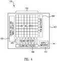
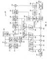
- Fig. 4illustrates a block diagram of infrared sensor assembly 128 including an array of infrared sensors 132 in accordance with an embodiment of the disclosure.
- infrared sensors 132are provided as part of a unit cell array of a ROIC 402.
- ROIC 402includes bias generation and timing control circuitry 404, column amplifiers 405, a column multiplexer 406, a row multiplexer 408, and an output amplifier 410.
- Image framese.g., thermal images
- processing module 160e.g., processor 195, and/or any other appropriate components to perform various processing techniques described herein.
- processor 195processor 195
- any desired array configurationmay be used in other embodiments.
- Infrared sensor assembly 128may capture images (e.g., image frames) and provide such images from its ROIC at various rates.
- Processing module 160may be used to perform appropriate processing of captured infrared images and may be implemented in accordance with any appropriate architecture.
- processing module 160may be implemented as an ASIC.
- such an ASICmay be configured to perform image processing with high performance and/or high efficiency.
- processing module 160may be implemented with a general purpose central processing unit (CPU) which may be configured to execute appropriate software instructions to perform image processing, coordinate and perform image processing with various image processing blocks, coordinate interfacing between processing module 160 and host device 102, and/or other operations.
- processing module 160may be implemented with a field programmable gate array (FPGA).
- processing module 160may also be implemented with other components where appropriate, such as, volatile memory, non-volatile memory, and/or one or more interfaces (e.g., infrared detector interfaces, inter-integrated circuit (I2C) interfaces, mobile industry processor interfaces (MIPI), joint test action group (JTAG) interfaces (e.g., IEEE 1149.1 standard test access port and boundary-scan architecture), and/or other interfaces).
- interfacese.g., infrared detector interfaces, inter-integrated circuit (I2C) interfaces, mobile industry processor interfaces (MIPI), joint test action group (JTAG) interfaces (e.g., IEEE 1149.1 standard test access port and boundary-scan architecture), and/or other interfaces).
- infrared imaging module 100may further include one or more actuators 199 which may be used to adjust the focus of infrared image frames captured by infrared sensor assembly 128.
- actuators 199may be used to move optical element 180, infrared sensors 132, and/or other components relative to each other to selectively focus and defocus infrared image frames in accordance with techniques described herein.
- Actuators 199may be implemented in accordance with any type of motion-inducing apparatus or mechanism, and may positioned at any location within or external to infrared imaging module 100 as appropriate for different applications.
- housing 120When infrared imaging module 100 is assembled, housing 120 may substantially enclose infrared sensor assembly 128, base 150, and processing module 160. Housing 120 may facilitate connection of various components of infrared imaging module 100. For example, in one embodiment, housing 120 may provide electrical connections 126 to connect various components as further described.
- Electrical connections 126may be electrically connected with bond pads 142 when infrared imaging module 100 is assembled.
- electrical connections 126may be embedded in housing 120, provided on inside surfaces of housing 120, and/or otherwise provided by housing 120. Electrical connections 126 may terminate in connections 124 protruding from the bottom surface of housing 120 as shown in Fig. 3 . Connections 124 may connect with circuit board 170 when infrared imaging module 100 is assembled (e.g., housing 120 may rest atop circuit board 170 in various embodiments).
- Processing module 160may be electrically connected with circuit board 170 through appropriate electrical connections.
- infrared sensor assembly 128may be electrically connected with processing module 160 through, for example, conductive electrical paths provided by: bond pads 142, complementary connections on inside surfaces of housing 120, electrical connections 126 of housing 120, connections 124, and circuit board 170.
- conductive electrical pathsprovided by: bond pads 142, complementary connections on inside surfaces of housing 120, electrical connections 126 of housing 120, connections 124, and circuit board 170.
- such an arrangementmay be implemented without requiring wire bonds to be provided between infrared sensor assembly 128 and processing module 160.
- electrical connections 126 in housing 120may be made from any desired material (e.g., copper or any other appropriate conductive material). In one embodiment, electrical connections 126 may aid in dissipating heat from infrared imaging module 100.
- sensor assembly 128may be attached to processing module 160 through a ceramic board that connects to sensor assembly 128 by wire bonds and to processing module 160 by a ball grid array (BGA).
- BGAball grid array
- sensor assembly 128may be mounted directly on a rigid flexible board and electrically connected with wire bonds, and processing module 160 may be mounted and connected to the rigid flexible board with wire bonds or a BGA.
- infrared imaging module 100 and host device 102set forth herein are provided for purposes of example, rather than limitation.
- any of the various techniques described hereinmay be applied to any infrared camera system, infrared imager, or other device for performing infrared/thermal imaging.
- Substrate 140 of infrared sensor assembly 128may be mounted on base 150.
- base 150e.g., a pedestal
- base 150may be made, for example, of copper formed by metal injection molding (MIM) and provided with a black oxide or nickel-coated finish.
- base 150may be made of any desired material, such as for example zinc, aluminum, or magnesium, as desired for a given application and may be formed by any desired applicable process, such as for example aluminum casting, MIM, or zinc rapid casting, as may be desired for particular applications.
- base 150may be implemented to provide structural support, various circuit paths, thermal heat sink properties, and other features where appropriate.
- base 150may be a multi-layer structure implemented at least in part using ceramic material.
- circuit board 170may receive housing 120 and thus may physically support the various components of infrared imaging module 100.
- circuit board 170may be implemented as a printed circuit board (e.g., an FR4 circuit board or other types of circuit boards), a rigid or flexible interconnect (e.g., tape or other type of interconnects), a flexible circuit substrate, a flexible plastic substrate, or other appropriate structures.
- base 150may be implemented with the various features and attributes described for circuit board 170, and vice versa.
- Socket 104may include a cavity 106 configured to receive infrared imaging module 100 (e.g., as shown in the assembled view of Fig. 2 ).
- Infrared imaging module 100 and/or socket 104may include appropriate tabs, arms, pins, fasteners, or any other appropriate engagement members which may be used to secure infrared imaging module 100 to or within socket 104 using friction, tension, adhesion, and/or any other appropriate manner.
- Socket 104may include engagement members 107 that may engage surfaces 109 of housing 120 when infrared imaging module 100 is inserted into a cavity 106 of socket 104. Other types of engagement members may be used in other embodiments.
- Infrared imaging module 100may be electrically connected with socket 104 through appropriate electrical connections (e.g., contacts, pins, wires, or any other appropriate connections).
- socket 104may include electrical connections 108 which may contact corresponding electrical connections of infrared imaging module 100 (e.g., interconnect pads, contacts, or other electrical connections on side or bottom surfaces of circuit board 170, bond pads 142 or other electrical connections on base 150, or other connections).
- Electrical connections 108may be made from any desired material (e.g., copper or any other appropriate conductive material).
- electrical connections 108may be mechanically biased to press against electrical connections of infrared imaging module 100 when infrared imaging module 100 is inserted into cavity 106 of socket 104.
- electrical connections 108may at least partially secure infrared imaging module 100 in socket 104. Other types of electrical connections may be used in other embodiments.
- Socket 104may be electrically connected with host device 102 through similar types of electrical connections.
- host device 102may include electrical connections (e.g., soldered connections, snap-in connections, or other connections) that connect with electrical connections 108 passing through apertures 190.
- electrical connectionsmay be made to the sides and/or bottom of socket 104.
- infrared imaging module 100may be implemented with flip chip technology which may be used to mount components directly to circuit boards without the additional clearances typically needed for wire bond connections.
- Flip chip connectionsmay be used, as an example, to reduce the overall size of infrared imaging module 100 for use in compact small form factor applications.
- processing module 160may be mounted to circuit board 170 using flip chip connections.
- infrared imaging module 100may be implemented with such flip chip configurations.
- infrared imaging module 100 and/or associated componentsmay be implemented in accordance with various techniques (e.g., wafer level packaging techniques) as set forth in U.S. Patent Application No. 12/844,124 filed July 27, 2010 , and U.S. Provisional Patent Application No. 61/469,651 filed March 30, 2011 .
- infrared imaging module 100 and/or associated componentsmay be implemented, calibrated, tested, and/or used in accordance with various techniques, such as for example as set forth in U.S. Patent No. 7,470,902 issued December 30, 2008 , U.S. Patent No. 6,028,309 issued February 22, 2000 , U.S. Patent No.
- host device 102may include shutter 105.
- shutter 105may be selectively positioned over socket 104 (e.g., as identified by arrows 103) while infrared imaging module 100 is installed therein.
- shutter 105may be used, for example, to protect infrared imaging module 100 when not in use.
- Shutter 105may also be used as a temperature reference as part of a calibration process (e.g., a NUC process or other calibration processes) for infrared imaging module 100 as would be understood by one skilled in the art.
- shutter 105may be made from various materials such as, for example, polymers, glass, aluminum (e.g., painted or anodized) or other materials.
- shutter 105may include one or more coatings to selectively filter electromagnetic radiation and/or adjust various optical properties of shutter 105 (e.g., a uniform blackbody coating or a reflective gold coating).
- shutter 105may be fixed in place to protect infrared imaging module 100 at all times.
- shutter 105 or a portion of shutter 105may be made from appropriate materials (e.g., polymers or infrared transmitting materials such as silicon, germanium, zinc selenide, or chalcogenide glasses) that do not substantially filter desired infrared wavelengths.
- a shuttermay be implemented as part of infrared imaging module 100 (e.g., within or as part of a lens barrel or other components of infrared imaging module 100), as would be understood by one skilled in the art.
- a shuttere.g., shutter 105 or other type of external or internal shutter
- a NUC process or other type of calibrationmay be performed using shutterless techniques.
- a NUC process or other type of calibration using shutterless techniquesmay be performed in combination with shutter-based techniques.
- Infrared imaging module 100 and host device 102may be implemented in accordance with any of the various techniques set forth in U.S. Provisional Patent Application No. 61/495,873 filed June 10, 2011 , U.S. Provisional Patent Application No. 61/495,879 filed June 10, 2011 , and U.S. Provisional Patent Application No. 61/495,888 filed June 10, 2011 .
- the components of host device 102 and/or infrared imaging module 100may be implemented as a local or distributed system with components in communication with each other over wired and/or wireless networks. Accordingly, the various operations identified in this disclosure may be performed by local and/or remote components as may be desired in particular implementations.
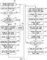
- Fig. 5illustrates a flow diagram of various operations to determine NUC terms in accordance with an embodiment of the disclosure.
- the operations of Fig. 5may be performed by processing module 160 or processor 195 (both also generally referred to as a processor) operating on image frames captured by infrared sensors 132.
- infrared sensors 132begin capturing image frames of a scene.
- the scenewill be the real world environment in which host device 102 is currently located.
- shutter 105if optionally provided
- Infrared sensors 132may continue capturing image frames during all operations shown in Fig. 5 .
- the continuously captured image framesmay be used for various operations as further discussed.
- the captured image framesmay be temporally filtered (e.g., in accordance with the process of block 826 further described herein with regard to Fig.
- a NUC process initiating eventis detected.
- the NUC processmay be initiated in response to physical movement of host device 102.
- Such movementmay be detected, for example, by motion sensors 194 which may be polled by a processor.
- a usermay move host device 102 in a particular manner, such as by intentionally waving host device 102 back and forth in an "erase” or "swipe" movement.
- the usermay move host device 102 in accordance with a predetermined speed and direction (velocity), such as in an up and down, side to side, or other pattern to initiate the NUC process.
- the use of such movementsmay permit the user to intuitively operate host device 102 to simulate the "erasing" of noise in captured image frames.
- a NUC processmay be initiated by host device 102 if motion exceeding a threshold value is exceeded (e.g., motion greater than expected for ordinary use). It is contemplated that any desired type of spatial translation of host device 102 may be used to initiate the NUC process.
- a threshold valuee.g., motion greater than expected for ordinary use. It is contemplated that any desired type of spatial translation of host device 102 may be used to initiate the NUC process.
- a NUC processmay be initiated by host device 102 if a minimum time has elapsed since a previously performed NUC process.
- a NUC processmay be initiated by host device 102 if infrared imaging module 100 has experienced a minimum temperature change since a previously performed NUC process.
- a NUC processmay be continuously initiated and repeated.
- the NUC processmay be selectively initiated based on whether one or more additional conditions are met. For example, in one embodiment, the NUC process may not be performed unless a minimum time has elapsed since a previously performed NUC process. In another embodiment, the NUC process may not be performed unless infrared imaging module 100 has experienced a minimum temperature change since a previously performed NUC process. Other criteria or conditions may be used in other embodiments. If appropriate criteria or conditions have been met, then the flow diagram continues to block 520. Otherwise, the flow diagram returns to block 505.
- blurred image framesmay be used to determine NUC terms which may be applied to captured image frames to correct for FPN.
- the blurred image framesmay be obtained by accumulating multiple image frames of a moving scene (e.g., captured while the scene and/or the thermal imager is in motion).
- the blurred image framesmay be obtained by defocusing an optical element or other component of the thermal imager.
- block 520a choice of either approach is provided. If the motion-based approach is used, then the flow diagram continues to block 525. If the defocus-based approach is used, then the flow diagram continues to block 530.
- motionis detected.
- motionmay be detected based on the image frames captured by infrared sensors 132.
- an appropriate motion detection processe.g., an image registration process, a frame-to-frame difference calculation, or other appropriate process
- itcan be determined whether pixels or regions around the pixels of consecutive image frames have changed more than a user defined amount (e.g., a percentage and/or threshold value). If at least a given percentage of pixels have changed by at least the user defined amount, then motion will be detected with sufficient certainty to proceed to block 535.
- a user defined amounte.g., a percentage and/or threshold value
- motionmay be determined on a per pixel basis, wherein only pixels that exhibit significant changes are accumulated to provide the blurred image frame.
- countersmay be provided for each pixel and used to ensure that the same number of pixel values are accumulated for each pixel, or used to average the pixel values based on the number of pixel values actually accumulated for each pixel.
- Other types of image-based motion detectionmay be performed such as performing a Radon transform.
- motionmay be detected based on data provided by motion sensors 194.
- motion detectionmay include detecting whether host device 102 is moving along a relatively straight trajectory through space. For example, if host device 102 is moving along a relatively straight trajectory, then it is possible that certain objects appearing in the imaged scene may not be sufficiently blurred (e.g., objects in the scene that may be aligned with or moving substantially parallel to the straight trajectory).
- the motion detected by motion sensors 194may be conditioned on host device 102 exhibiting, or not exhibiting, particular trajectories.
- both a motion detection process and motion sensors 194may be used.
- a determinationcan be made as to whether or not each image frame was captured while at least a portion of the scene and host device 102 were in motion relative to each other (e.g., which may be caused by host device 102 moving relative to the scene, at least a portion of the scene moving relative to host device 102, or both).
- the image frames for which motion was detectedmay exhibit some secondary blurring of the captured scene (e.g., blurred thermal image data associated with the scene) due to the thermal time constants of infrared sensors 132 (e.g., microbolometer thermal time constants) interacting with the scene movement.
- some secondary blurring of the captured scenee.g., blurred thermal image data associated with the scene
- thermal time constants of infrared sensors 132e.g., microbolometer thermal time constants
- image frames for which motion was detectedare accumulated. For example, if motion is detected for a continuous series of image frames, then the image frames of the series may be accumulated. As another example, if motion is detected for only some image frames, then the non-moving image frames may be skipped and not included in the accumulation. Thus, a continuous or discontinuous set of image frames may be selected to be accumulated based on the detected motion.
- the accumulated image framesare averaged to provide a blurred image frame. Because the accumulated image frames were captured during motion, it is expected that actual scene information will vary between the image frames and thus cause the scene information to be further blurred in the resulting blurred image frame (block 545).
- FPNe.g., caused by one or more components of infrared imaging module 100
- FPNwill remain fixed over at least short periods of time and over at least limited changes in scene irradiance during motion.
- image frames captured in close proximity in time and space during motionwill suffer from identical or at least very similar FPN.
- scene informationmay change in consecutive image frames, the FPN will stay essentially constant.
- multiple image frames captured during motionwill blur the scene information, but will not blur the FPN.
- FPNwill remain more clearly defined in the blurred image frame provided in block 545 than the scene information.
- 32 or more image framesare accumulated and averaged in blocks 535 and 540.
- any desired number of image framesmay be used in other embodiments, but with generally decreasing correction accuracy as frame count is decreased.
- a defocus operationmay be performed to intentionally defocus the image frames captured by infrared sensors 132.
- one or more actuators 199may be used to adjust, move, or otherwise translate optical element 180, infrared sensor assembly 128, and/or other components of infrared imaging module 100 to cause infrared sensors 132 to capture a blurred (e.g., unfocused) image frame of the scene.
- Other non-actuator based techniquesare also contemplated for intentionally defocusing infrared image frames such as, for example, manual (e.g., user-initiated) defocusing.
- FPNe.g., caused by one or more components of infrared imaging module 100
- FPNwill remain unaffected by the defocusing operation.
- a blurred image frame of the scenewill be provided (block 545) with FPN remaining more clearly defined in the blurred image than the scene information.
- the defocus-based approachhas been described with regard to a single captured image frame.
- the defocus-based approachmay include accumulating multiple image frames while the infrared imaging module 100 has been defocused and averaging the defocused image frames to remove the effects of temporal noise and provide a blurred image frame in block 545.
- a blurred image framemay be provided in block 545 by either the motion-based approach or the defocus-based approach. Because much of the scene information will be blurred by either motion, defocusing, or both, the blurred image frame may be effectively considered a low pass filtered version of the original captured image frames with respect to scene information.
- the blurred image frameis processed to determine updated row and column FPN terms (e.g., if row and column FPN terms have not been previously determined then the updated row and column FPN terms may be new row and column FPN terms in the first iteration of block 550).
- updated row and column FPN termse.g., if row and column FPN terms have not been previously determined then the updated row and column FPN terms may be new row and column FPN terms in the first iteration of block 550.
- the terms row and columnmay be used interchangeably depending on the orientation of infrared sensors 132 and/or other components of infrared imaging module 100.
- block 550includes determining a spatial FPN correction term for each row of the blurred image frame (e.g., each row may have its own spatial FPN correction term), and also determining a spatial FPN correction term for each column of the blurred image frame (e.g., each column may have its own spatial FPN correction term).
- Such processingmay be used to reduce the spatial and slowly varying (1/f) row and column FPN inherent in thermal imagers caused by, for example, 1/f noise characteristics of amplifiers in ROIC 402 which may manifest as vertical and horizontal stripes in image frames.
- row and column FPN termsmay be determined by considering differences between neighboring pixels of the blurred image frame.
- Fig. 6illustrates differences between neighboring pixels in accordance with an embodiment of the disclosure. Specifically, in Fig. 6 a pixel 610 is compared to its 8 nearest horizontal neighbors: d0-d3 on one side and d4-d7 on the other side. Differences between the neighbor pixels can be averaged to obtain an estimate of the offset error of the illustrated group of pixels. An offset error may be calculated for each pixel in a row or column and the average result may be used to correct the entire row or column.
- threshold valuesmay be used (thPix and -thPix). Pixel values falling outside these threshold values (pixels d1 and d4 in this example) are not used to obtain the offset error.
- the maximum amount of row and column FPN correctionmay be limited by these threshold values.
- the updated row and column FPN terms determined in block 550are stored (block 552) and applied (block 555) to the blurred image frame provided in block 545. After these terms are applied, some of the spatial row and column FPN in the blurred image frame may be reduced. However, because such terms are applied generally to rows and columns, additional FPN may remain such as spatially uncorrelated FPN associated with pixel to pixel drift or other causes. Neighborhoods of spatially correlated FPN may also remain which may not be directly associated with individual rows and columns. Accordingly, further processing may be performed as discussed below to determine NUC terms.
- local contrast valuese.g., edges or absolute values of gradients between adjacent or small groups of pixels
- scene information in the blurred image frameincludes contrasting areas that have not been significantly blurred (e.g., high contrast edges in the original scene data)
- contrasting arease.g., high contrast edges in the original scene data
- local contrast values in the blurred image framemay be calculated, or any other desired type of edge detection process may be applied to identify certain pixels in the blurred image as being part of an area of local contrast. Pixels that are marked in this manner may be considered as containing excessive high spatial frequency scene information that would be interpreted as FPN (e.g., such regions may correspond to portions of the scene that have not been sufficiently blurred). As such, these pixels may be excluded from being used in the further determination of NUC terms.
- contrast detection processingmay rely on a threshold that is higher than the expected contrast value associated with FPN (e.g., pixels exhibiting a contrast value higher than the threshold may be considered to be scene information, and those lower than the threshold may be considered to be exhibiting FPN).
- the contrast determination of block 560may be performed on the blurred image frame after row and column FPN terms have been applied to the blurred image frame (e.g., as shown in Fig. 5 ). In another embodiment, block 560 may be performed prior to block 550 to determine contrast before row and column FPN terms are determined (e.g., to prevent scene based contrast from contributing to the determination of such terms).
- any high spatial frequency content remaining in the blurred image framemay be generally attributed to spatially uncorrelated FPN.
- much of the other noise or actual desired scene based informationhas been removed or excluded from the blurred image frame due to: intentional blurring of the image frame (e.g., by motion or defocusing in blocks 520 through 545), application of row and column FPN terms (block 555), and contrast determination (block 560).
- any remaining high spatial frequency contentmay be attributed to spatially uncorrelated FPN.
- the blurred image frameis high pass filtered. In one embodiment, this may include applying a high pass filter to extract the high spatial frequency content from the blurred image frame. In another embodiment, this may include applying a low pass filter to the blurred image frame and taking a difference between the low pass filtered image frame and the unfiltered blurred image frame to obtain the high spatial frequency content.
- a high pass filtermay be implemented by calculating a mean difference between a sensor signal (e.g., a pixel value) and its neighbors.
- a flat field correction processis performed on the high pass filtered blurred image frame to determine updated NUC terms (e.g., if a NUC process has not previously been performed then the updated NUC terms may be new NUC terms in the first iteration of block 570).
- Fig. 7illustrates a flat field correction technique 700 in accordance with an embodiment of the disclosure.
- a NUC termmay be determined for each pixel 710 of the blurred image frame using the values of its neighboring pixels 712 to 726.
- several gradientsmay be determined based on the absolute difference between the values of various adjacent pixels. For example, absolute value differences may be determined between: pixels 712 and 714 (a left to right diagonal gradient), pixels 716 and 718 (a top to bottom vertical gradient), pixels 720 and 722 (a right to left diagonal gradient), and pixels 724 and 726 (a left to right horizontal gradient).
- a weight valuemay be determined for pixel 710 that is inversely proportional to the summed gradient. This process may be performed for all pixels 710 of the blurred image frame until a weight value is provided for each pixel 710. For areas with low gradients (e.g., areas that are blurry or have low contrast), the weight value will be close to one. Conversely, for areas with high gradients, the weight value will be zero or close to zero. The update to the NUC term as estimated by the high pass filter is multiplied with the weight value.
- the risk of introducing scene information into the NUC termscan be further reduced by applying some amount of temporal damping to the NUC term determination process.
- a temporal damping factor ⁇ between 0 and 1may be chosen such that the new NUC term (NUC NEW ) stored is a weighted average of the old NUC term (NUC OLD ) and the estimated updated NUC term (NUC UPDATE ).
- block 570may include additional processing of the NUC terms. For example, in one embodiment, to preserve the scene signal mean, the sum of all NUC terms may be normalized to zero by subtracting the NUC term mean from each NUC term.
- the mean value of each row and columnmay be subtracted from the NUC terms for each row and column.
- row and column FPN filters using the row and column FPN terms determined in block 550may be better able to filter out row and column noise in further iterations (e.g., as further shown in Fig. 8 ) after the NUC terms are applied to captured images (e.g., in block 580 further discussed herein).
- the row and column FPN filtersmay in general use more data to calculate the per row and per column offset coefficients (e.g., row and column FPN terms) and may thus provide a more robust alternative for reducing spatially correlated FPN than the NUC terms which are based on high pass filtering to capture spatially uncorrelated noise.
- additional high pass filtering and further determinations of updated NUC termsmay be optionally performed to remove spatially correlated FPN with lower spatial frequency than previously removed by row and column FPN terms.
- some variability in infrared sensors 132 or other components of infrared imaging module 100may result in spatially correlated FPN noise that cannot be easily modeled as row or column noise.
- Such spatially correlated FPNmay include, for example, window defects on a sensor package or a cluster of infrared sensors 132 that respond differently to irradiance than neighboring infrared sensors 132.
- such spatially correlated FPNmay be mitigated with an offset correction.
- the noisemay also be detectable in the blurred image frame. Since this type of noise may affect a neighborhood of pixels, a high pass filter with a small kernel may not detect the FPN in the neighborhood (e.g., all values used in high pass filter may be taken from the neighborhood of affected pixels and thus may be affected by the same offset error). For example, if the high pass filtering of block 565 is performed with a small kernel (e.g., considering only immediately adjacent pixels that fall within a neighborhood of pixels affected by spatially correlated FPN), then broadly distributed spatially correlated FPN may not be detected.
- a small kernele.g., considering only immediately adjacent pixels that fall within a neighborhood of pixels affected by spatially correlated FPN
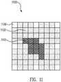
- Fig. 11illustrates spatially correlated FPN in a neighborhood of pixels in accordance with an embodiment of the disclosure.
- a neighborhood of pixels 1110may exhibit spatially correlated FPN that is not precisely correlated to individual rows and columns and is distributed over a neighborhood of several pixels (e.g., a neighborhood of approximately 4 by 4 pixels in this example).
- Sample image frame 1100also includes a set of pixels 1120 exhibiting substantially uniform response that are not used in filtering calculations, and a set of pixels 1130 that are used to estimate a low pass value for the neighborhood of pixels 1110.
- pixels 1130may be a number of pixels divisible by two in order to facilitate efficient hardware or software calculations.
- additional high pass filtering and further determinations of updated NUC termsmay be optionally performed to remove spatially correlated FPN such as exhibited by pixels 1110.
- the updated NUC terms determined in block 570are applied to the blurred image frame.
- the blurred image framewill have been initially corrected for spatially correlated FPN (e.g., by application of the updated row and column FPN terms in block 555), and also initially corrected for spatially uncorrelated FPN (e.g., by application of the updated NUC terms applied in block 571).
- a further high pass filteris applied with a larger kernel than was used in block 565, and further updated NUC terms may be determined in block 573.
- the high pass filter applied in block 572may include data from a sufficiently large enough neighborhood of pixels such that differences can be determined between unaffected pixels (e.g., pixels 1120) and affected pixels (e.g., pixels 1110).
- a low pass filter with a large kernelcan be used (e.g., an N by N kernel that is much greater than 3 by 3 pixels) and the results may be subtracted to perform appropriate high pass filtering.
- a sparse kernelmay be used such that only a small number of neighboring pixels inside an N by N neighborhood are used.
- the temporal damping factor ⁇may be set close to 1 for updated NUC terms determined in block 573.
- blocks 571-573may be repeated (e.g., cascaded) to iteratively perform high pass filtering with increasing kernel sizes to provide further updated NUC terms further correct for spatially correlated FPN of desired neighborhood sizes.
- the decision to perform such iterationsmay be determined by whether spatially correlated FPN has actually been removed by the updated NUC terms of the previous performance of blocks 571-573.
- thresholding criteriamay be applied to individual pixels to determine which pixels receive updated NUC terms.
- the threshold valuesmay correspond to differences between the newly calculated NUC terms and previously calculated NUC terms.
- the threshold valuesmay be independent of previously calculated NUC terms. Other tests may be applied (e.g., spatial correlation tests) to determine whether the NUC terms should be applied.
- the flow diagramreturns to block 505. Otherwise, the newly determined NUC terms are stored (block 575) to replace previous NUC terms (e.g., determined by a previously performed iteration of Fig. 5 ) and applied (block 580) to captured image frames.
- Fig. 8illustrates various image processing techniques of Fig. 5 and other operations applied in an image processing pipeline 800 in accordance with an embodiment of the disclosure.
- pipeline 800identifies various operations of Fig. 5 in the context of an overall iterative image processing scheme for correcting image frames provided by infrared imaging module 100.
- pipeline 800may be provided by processing module 160 or processor 195 (both also generally referred to as a processor) operating on image frames captured by infrared sensors 132.
- Image frames captured by infrared sensors 132may be provided to a frame averager 804 that integrates multiple image frames to provide image frames 802 with an improved signal to noise ratio.
- Frame averager 804may be effectively provided by infrared sensors 132, ROIC 402, and other components of infrared sensor assembly 128 that are implemented to support high image capture rates.
- infrared sensor assembly 128may capture infrared image frames at a frame rate of 240 Hz (e.g., 240 images per second).
- such a high frame ratemay be implemented, for example, by operating infrared sensor assembly 128 at relatively low voltages (e.g., compatible with mobile telephone voltages) and by using a relatively small array of infrared sensors 132 (e.g., an array of 64 by 64 infrared sensors in one embodiment).
- relatively low voltagese.g., compatible with mobile telephone voltages
- infrared sensors 132e.g., an array of 64 by 64 infrared sensors in one embodiment
- such infrared image framesmay be provided from infrared sensor assembly 128 to processing module 160 at a high frame rate (e.g., 240 Hz or other frame rates).
- infrared sensor assembly 128may integrate over longer time periods, or multiple time periods, to provide integrated (e.g., averaged) infrared image frames to processing module 160 at a lower frame rate (e.g., 30 Hz, 9 Hz, or other frame rates). Further information regarding implementations that may be used to provide high image capture rates may be found in U.S. Provisional Patent Application No. 61/495,879 previously referenced herein.
- Image frames 802proceed through pipeline 800 where they are adjusted by various terms, temporally filtered, used to determine the various adjustment terms, and gain compensated.
- factory gain terms 812 and factory offset terms 816are applied to image frames 802 to compensate for gain and offset differences, respectively, between the various infrared sensors 132 and/or other components of infrared imaging module 100 determined during manufacturing and testing.
- NUC terms 817are applied to image frames 802 to correct for FPN as discussed.
- block 580may not be performed or initialization values may be used for NUC terms 817 that result in no alteration to the image data (e.g., offsets for every pixel would be equal to zero).
- column FPN terms 820 and row FPN terms 824are applied to image frames 802.
- Column FPN terms 820 and row FPN terms 824may be determined in accordance with block 550 as discussed. In one embodiment, if the column FPN terms 820 and row FPN terms 824 have not yet been determined (e.g., before a NUC process has been initiated), then blocks 818 and 822 may not be performed or initialization values may be used for the column FPN terms 820 and row FPN terms 824 that result in no alteration to the image data (e.g., offsets for every pixel would be equal to zero).
- temporal filteringis performed on image frames 802 in accordance with a temporal noise reduction (TNR) process.
- Fig. 9illustrates a TNR process in accordance with an embodiment of the disclosure.
- Image frames 802a and 802binclude local neighborhoods of pixels 803a and 803b centered around pixels 805a and 805b, respectively. Neighborhoods 803a and 803b correspond to the same locations within image frames 802a and 802b and are subsets of the total pixels in image frames 802a and 802b.
- neighborhoods 803a and 803binclude areas of 5 by 5 pixels. Other neighborhood sizes may be used in other embodiments.
- Averaged delta value 805cmay be used to determine weight values in block 807 to be applied to pixels 805a and 805b of image frames 802a and 802b.
- the weight values determined in block 807may be inversely proportional to averaged delta value 805c such that weight values drop rapidly towards zero when there are large differences between neighborhoods 803a and 803b.
- large differences between neighborhoods 803a and 803bmay indicate that changes have occurred within the scene (e.g., due to motion) and pixels 802a and 802b may be appropriately weighted, in one embodiment, to avoid introducing blur across frame-to-frame scene changes.
- Other associations between weight values and averaged delta value 805cmay be used in various embodiments.
- the weight values determined in block 807may be applied to pixels 805a and 805b to determine a value for corresponding pixel 805e of image frame 802e (block 811).
- pixel 805emay have a value that is a weighted average (or other combination) of pixels 805a and 805b, depending on averaged delta value 805c and the weight values determined in block 807.
- pixel 805e of temporally filtered image frame 802emay be a weighted sum of pixels 805a and 805b of image frames 802a and 802b. If the average difference between pixels 805a and 805b is due to noise, then it may be expected that the average change between neighborhoods 805a and 805b will be close to zero (e.g., corresponding to the average of uncorrelated changes). Under such circumstances, it may be expected that the sum of the differences between neighborhoods 805a and 805b will be close to zero. In this case, pixel 805a of image frame 802a may both be appropriately weighted so as to contribute to the value of pixel 805e.
- averaged delta value 805chas been described as being determined based on neighborhoods 805a and 805b, in other embodiments averaged delta value 805c may be determined based on any desired criteria (e.g., based on individual pixels or other types of groups of sets of pixels).
- image frame 802ahas been described as a presently received image frame and image frame 802b has been described as a previously temporally filtered image frame.
- image frames 802a and 802bmay be first and second image frames captured by infrared imaging module 100 that have not been temporally filtered.
- Fig. 10illustrates further implementation details in relation to the TNR process of block 826.
- image frames 802a and 802bmay be read into line buffers 1010a and 1010b, respectively, and image frame 802b (e.g., the previous image frame) may be stored in a frame buffer 1020 before being read into line buffer 1010b.
- line buffers 1010a-b and frame buffer 1020may be implemented by a block of random access memory (RAM) provided by any appropriate component of infrared imaging module 100 and/or host device 102.
- RAMrandom access memory
- image frame 802emay be passed to an automatic gain compensation block 828 for further processing to provide a result image frame 830 that may be used by host device 102 as desired.
- Fig. 8further illustrates various operations that may be performed to determine row and column FPN terms and NUC terms as discussed.
- these operationsmay use image frames 802e as shown in Fig. 8 . Because image frames 802e have already been temporally filtered, at least some temporal noise may be removed and thus will not inadvertently affect the determination of row and column FPN terms 824 and 820 and NUC terms 817.
- non-temporally filtered image frames 802may be used.
- a NUC processmay be selectively initiated and performed in response to various NUC process initiating events and based on various criteria or conditions.
- the NUC processmay be performed in accordance with a motion-based approach (blocks 525, 535, and 540) or a defocus-based approach (block 530) to provide a blurred image frame (block 545).
- Fig. 8further illustrates various additional blocks 550, 552, 555, 560, 565, 570, 571, 572, 573, and 575 previously discussed with regard to Fig. 5 .
- row and column FPN terms 824 and 820 and NUC terms 817may be determined and applied in an iterative fashion such that updated terms are determined using image frames 802 to which previous terms have already been applied. As a result, the overall process of Fig. 8 may repeatedly update and apply such terms to continuously reduce the noise in image frames 830 to be used by host device 102.
- blocks 525, 535, and 540are shown as operating at the normal frame rate of image frames 802 received by pipeline 800.
- the determination made in block 525is represented as a decision diamond used to determine whether a given image frame 802 has sufficiently changed such that it may be considered an image frame that will enhance the blur if added to other image frames and is therefore accumulated (block 535 is represented by an arrow in this embodiment) and averaged (block 540).
- column FPN terms 820(block 550) is shown as operating at an update rate that in this example is 1/32 of the sensor frame rate (e.g., normal frame rate) due to the averaging performed in block 540. Other update rates may be used in other embodiments. Although only column FPN terms 820 are identified in Fig. 10 , row FPN terms 824 may be implemented in a similar fashion at the reduced frame rate.
- Fig. 10also illustrates further implementation details in relation to the NUC determination process of block 570.
- the blurred image framemay be read to a line buffer 1030 (e.g., implemented by a block of RAM provided by any appropriate component of infrared imaging module 100 and/or host device 102).
- the flat field correction technique 700 of Fig. 7may be performed on the blurred image frame.
- FPNFPN
- techniques described hereinmay be used to remove various types of FPN (e.g., including very high amplitude FPN) such as spatially correlated row and column FPN and spatially uncorrelated FPN.
- the rate at which row and column FPN terms and/or NUC terms are updatedcan be inversely proportional to the estimated amount of blur in the blurred image frame and/or inversely proportional to the magnitude of local contrast values (e.g., determined in block 560).
- the described techniquesmay provide advantages over conventional shutter-based noise correction techniques.
- a shuttere.g., such as shutter 105
- Power and maximum voltage supplied to, or generated by, infrared imaging module 100may also be reduced if a shutter does not need to be mechanically operated. Reliability will be improved by removing the shutter as a potential point of failure.
- a shutterless processalso eliminates potential image interruption caused by the temporary blockage of the imaged scene by a shutter.
- noise correctionmay be performed on image frames that have irradiance levels similar to those of the actual scene desired to be imaged. This can improve the accuracy and effectiveness of noise correction terms determined in accordance with the various described techniques.
- infrared imaging module 100may be configured to operate at low voltage levels.
- infrared imaging module 100may be implemented with circuitry configured to operate at low power and/or in accordance with other parameters that permit infrared imaging module 100 to be conveniently and effectively implemented in various types of host devices 102, such as mobile devices and other devices.
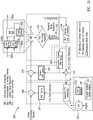
- Fig. 12illustrates a block diagram of another implementation of infrared sensor assembly 128 including infrared sensors 132 and an LDO 1220 in accordance with an embodiment of the disclosure.
- Fig. 12also illustrates various components 1202, 1204, 1205, 1206, 1208, and 1210 which may implemented in the same or similar manner as corresponding components previously described with regard to Fig. 4 .
- Fig. 12also illustrates bias correction circuitry 1212 which may be used to adjust one or more bias voltages provided to infrared sensors 132 (e.g., to compensate for temperature changes, self-heating, and/or other factors).
- LDO 1220may be provided as part of infrared sensor assembly 128 (e.g., on the same chip and/or wafer level package as the ROIC).
- LDO 1220may be provided as part of an FPA with infrared sensor assembly 128.
- such implementationsmay reduce power supply noise introduced to infrared sensor assembly 128 and thus provide an improved PSRR.
- by implementing the LDO with the ROICless die area may be consumed and fewer discrete die (or chips) are needed.
- LDO 1220receives an input voltage provided by a power source 1230 over a supply line 1232.
- LDO 1220provides an output voltage to various components of infrared sensor assembly 128 over supply lines 1222.
- LDO 1220may provide substantially identical regulated output voltages to various components of infrared sensor assembly 128 in response to a single input voltage received from power source 1230.
- power source 1230may provide an input voltage in a range of approximately 2.8 volts to approximately 11 volts (e.g., approximately 2.8 volts in one embodiment), and LDO 1220 may provide an output voltage in a range of approximately 1.5 volts to approximately 2.8 volts (e.g., approximately 2.5 volts in one embodiment).
- LDO 1220may be used to provide a consistent regulated output voltage, regardless of whether power source 1230 is implemented with a conventional voltage range of approximately 9 volts to approximately 11 volts, or a low voltage such as approximately 2.8 volts.
- the output voltage of LDO 1220will remain fixed despite changes in the input voltage.
- LDO 1220as part of infrared sensor assembly 128 provides various advantages over conventional power implementations for FPAs.
- conventional FPAstypically rely on multiple power sources, each of which may be provided separately to the FPA, and separately distributed to the various components of the FPA.
- appropriate voltagesmay be separately provided (e.g., to reduce possible noise) to all components of infrared sensor assembly 128 with reduced complexity.
- LDO 1220also allows infrared sensor assembly 128 to operate in a consistent manner, even if the input voltage from power source 1230 changes (e.g., if the input voltage increases or decreases as a result of charging or discharging a battery or other type of device used for power source 1230).
- LDO 1220may be implemented to provide a low voltage (e.g., approximately 2.5 volts). This contrasts with the multiple higher voltages typically used to power conventional FPAs, such as: approximately 3.3 volts to approximately 5 volts used to power digital circuitry; approximately 3.3 volts used to power analog circuitry; and approximately 9 volts to approximately 11 volts used to power loads. Also, in some embodiments, the use of LDO 1220 may reduce or eliminate the need for a separate negative reference voltage to be provided to infrared sensor assembly 128.
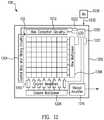
- Fig. 13illustrates a circuit diagram of a portion of infrared sensor assembly 128 of Fig. 12 in accordance with an embodiment of the disclosure.
- Fig. 13illustrates additional components of bias correction circuitry 1212 (e.g., components 1326, 1330, 1332, 1334, 1336, 1338, and 1341) connected to LDO 1220 and infrared sensors 132.
- bias correction circuitry 1212may be used to compensate for temperature-dependent changes in bias voltages in accordance with an embodiment of the present disclosure.
- the operation of such additional componentsmay be further understood with reference to similar components identified in U.S. Patent No.
- Infrared sensor assembly 128may also be implemented in accordance with the various components identified in U.S. Patent No. 6,812,465 issued November 2, 2004 .
- some or all of the bias correction circuitry 1212may be implemented on a global array basis as shown in Fig. 13 (e.g., used for all infrared sensors 132 collectively in an array).
- some or all of the bias correction circuitry 1212may be implemented an individual sensor basis (e.g., entirely or partially duplicated for each infrared sensor 132).
- bias correction circuitry 1212 and other components of Fig. 13may be implemented as part of ROIC 1202.
- LDO 1220provides a load voltage Vload to bias correction circuitry 1212 along one of supply lines 1222.
- Vloadmay be approximately 2.5 volts which contrasts with larger voltages of approximately 9 volts to approximately 11 volts that may be used as load voltages in conventional infrared imaging devices.
- bias correction circuitry 1212Based on Vload, bias correction circuitry 1212 provides a sensor bias voltage Vbolo at a node 1360.
- Vbolomay be distributed to one or more infrared sensors 132 through appropriate switching circuitry 1370 (e.g., represented by broken lines in Fig. 13 ).
- switching circuitry 1370may be implemented in accordance with appropriate components identified in U.S. Patent Nos. 6,812,465 and 7,679,048 previously referenced herein.
- Each infrared sensor 132includes a node 1350 which receives Vbolo through switching circuitry 1370, and another node 1352 which may be connected to ground, a substrate, and/or a negative reference voltage.
- the voltage at node 1360may be substantially the same as Vbolo provided at nodes 1350. In other embodiments, the voltage at node 1360 may be adjusted to compensate for possible voltage drops associated with switching circuitry 1370 and/or other factors.
- Vbolomay be implemented with lower voltages than are typically used for conventional infrared sensor biasing. In one embodiment, Vbolo may be in a range of approximately 0.2 volts to approximately 0.7 volts. In another embodiment, Vbolo may be in a range of approximately 0.4 volts to approximately 0.6 volts. In another embodiment, Vbolo may be approximately 0.5 volts. In contrast, conventional infrared sensors typically use bias voltages of approximately 1 volt.
- infrared sensor assembly 128permits infrared sensor assembly 128 to exhibit significantly reduced power consumption in comparison with conventional infrared imaging devices.
- the power consumption of each infrared sensor 132is reduced by the square of the bias voltage.
- a reduction from, for example, 1.0 volt to 0.5 voltsprovides a significant reduction in power, especially when applied to many infrared sensors 132 in an infrared sensor array. This reduction in power may also result in reduced self-heating of infrared sensor assembly 128.
- various techniquesare provided for reducing the effects of noise in image frames provided by infrared imaging devices operating at low voltages.
- noise, self-heating, and/or other phenomenamay, if uncorrected, become more pronounced in image frames provided by infrared sensor assembly 128.
- Vbolowhen LDO 1220 maintains Vload at a low voltage in the manner described herein, Vbolo will also be maintained at its corresponding low voltage and the relative size of its output signals may be reduced. As a result, noise, self-heating, and/or other phenomena may have a greater effect on the smaller output signals read out from infrared sensors 132, resulting in variations (e.g., errors) in the output signals. If uncorrected, these variations may be exhibited as noise in the image frames.
- low voltage operationmay reduce the overall amount of certain phenomena (e.g., self-heating)
- the smaller output signalsmay permit the remaining error sources (e.g., residual self-heating) to have a disproportionate effect on the output signals during low voltage operation.
- infrared sensor assembly 128, infrared imaging module 100, and/or host device 102may be implemented with various array sizes, frame rates, and/or frame averaging techniques.
- infrared sensors 132may be implemented with array sizes ranging from 32 by 32 to 160 by 120 infrared sensors 132.
- Other example array sizesinclude 80 by 64, 80 by 60, 64 by 64, and 64 by 32. Any desired array size may be used.
- infrared sensor assembly 128may provide image frames at relatively high frame rates without requiring significant changes to ROIC and related circuitry.
- frame ratesmay range from approximately 120 Hz to approximately 480 Hz.
- the array size and the frame ratemay be scaled relative to each other (e.g., in an inversely proportional manner or otherwise) such that larger arrays are implemented with lower frame rates, and smaller arrays are implemented with higher frame rates.
- an array of 160 by 120may provide a frame rate of approximately 120 Hz.
- an array of 80 by 60may provide a correspondingly higher frame rate of approximately 240 Hz.
- Other frame ratesare also contemplated.
- the particular readout timing of rows and/or columns of the FPA arraymay remain consistent, regardless of the actual FPA array size or frame rate.
- the readout timingmay be approximately 63 microseconds per row or column.
- the image frames captured by infrared sensors 132may be provided to a frame averager 804 that integrates multiple image frames to provide image frames 802 (e.g., processed image frames) with a lower frame rate (e.g., approximately 30 Hz, approximately 60 Hz, or other frame rates) and with an improved signal to noise ratio.
- image frames 802e.g., processed image frames
- a lower frame ratee.g., approximately 30 Hz, approximately 60 Hz, or other frame rates
- image noise attributable to low voltage operationmay be effectively averaged out and/or substantially reduced in image frames 802.
- infrared sensor assembly 128may be operated at relatively low voltages provided by LDO 1220 as discussed without experiencing additional noise and related side effects in the resulting image frames 802 after processing by frame averager 804.
- infrared sensors 132may be used together to provide higher resolution image frames (e.g., a scene may be imaged across multiple such arrays).
- Such arraysmay be provided in multiple infrared sensor assemblies 128 and/or provided in the same infrared sensor assembly 128. Each such array may be operated at low voltages as described, and also may be provided with associated ROIC circuitry such that each array may still be operated at a relatively high frame rate.
- the high frame rate image frames provided by such arraysmay be averaged by shared or dedicated frame averagers 804 to reduce and/or eliminate noise associated with low voltage operation. As a result, high resolution infrared images may be obtained while still operating at low voltages.
- infrared sensor assembly 128may be implemented with appropriate dimensions to permit infrared imaging module 100 to be used with a small form factor socket 104, such as a socket used for mobile devices.
- infrared sensor assembly 128may be implemented with a chip size in a range of approximately 4.0 mm by approximately 4.0 mm to approximately 5.5 mm by approximately 5.5 mm (e.g., approximately 4.0 mm by approximately 5.5 mm in one example).
- Infrared sensor assembly 128may be implemented with such sizes or other appropriate sizes to permit use with socket 104 implemented with various sizes such as: 8.5 mm by 8.5 mm, 8.5 mm by 5.9 mm, 6.0 mm by 6.0 mm, 5.5 mm by 5.5 mm, 4.5 mm by 4.5 mm, and/or other socket sizes such as, for example, those identified in Table 1 of U.S. Provisional Patent Application No. 61/495,873 previously referenced herein.
- Non-transitory instructions, program code, and/or datacan be stored on one or more non-transitory machine readable mediums. It is also contemplated that software identified herein can be implemented using one or more general purpose or specific purpose computers and/or computer systems, networked and/or otherwise. Where applicable, the ordering of various steps described herein can be changed, combined into composite steps, and/or separated into sub-steps to provide features described herein.
Landscapes
- Engineering & Computer Science (AREA)
- Multimedia (AREA)
- Signal Processing (AREA)
- Transforming Light Signals Into Electric Signals (AREA)
- Studio Devices (AREA)
- Photometry And Measurement Of Optical Pulse Characteristics (AREA)
- Solid State Image Pick-Up Elements (AREA)
Description
- One or more embodiments of the invention relate generally to thermal imaging devices and more particularly, for example, to the implementation and operation of such devices in a manner appropriate for low power and small form factor applications.
- Infrared imaging devices, such as infrared cameras or other devices, are typically implemented with an array of infrared sensors. However, existing infrared sensors and related circuitry are typically sensitive to noise and other phenomena. Because of such sensitivity, infrared sensors and related circuitry are often implemented with power supply arrangements wherein multiple voltage supply paths provide different voltages to various circuit components. However, such implementations are typically complex and may be relatively inefficient.
- In addition, during operation at conventional voltages and currents, infrared imaging devices may experience significant self-heating which may cause various undesirable thermal effects. Nevertheless, conventional techniques to reduce such effects are also less than ideal and may rely on active cooling or other measures that increase the cost and complexity of infrared imaging devices.
- Document
US 2002/058352 A1 discloses a two-dimensional array of Lead-Salt detector elements monolithically formed and mounted on an integrated circuit that includes an integrated circuit having a passivation layer and a plurality of electrical contacts. The system also includes a delineated, sensitized Lead-Salt layer upon the passivation layer, the delineations forming a plurality of detector elements. The system additionally includes vias through the passivation layer to the electrical contacts and electrical couplers between the electrical contacts and the detector elements. DocumentUS 6444983 B1 discloses a common structure of a FPA comprising an array of microbolometers, a bias voltage circuit and a ROIC. A bias voltage of the similar system of document XP055345084 is 1,6 V while the bias voltage range used by the similar system of document XP055345096 is 2-8 V. - Various techniques are provided for implementing and operating infrared imaging devices, especially for low power and small form factor applications. In one embodiment, a system includes a focal plane array (FPA) comprising: an array of infrared sensors adapted to image a scene; a bias circuit adapted to provide a bias voltage to the infrared sensors, wherein the bias voltage is selected from a range of approximately 0.2 volts to approximately 0.7 volts; and a read out integrated circuit (ROIC) adapted to provide signals from the infrared sensors corresponding to captured image frames.
- In another embodiment, a system includes a focal plane array (FPA) comprising: an array of infrared sensors adapted to image a scene, wherein a size of the array of infrared sensors is less than approximately 160 by 120; and a read out integrated circuit (ROIC) adapted to provide signals from the infrared sensors corresponding to captured image frames, wherein the ROIC is adapted to provide the captured image frames at a frame rate selected from a range of approximately 120 Hz to approximately 480 Hz.
- In another embodiment, a method includes providing a bias voltage from a bias circuit of a focal plane array (FPA) to an array of infrared sensors of the FPA, wherein the bias voltage is selected from a range of approximately 0.2 volts to approximately 0.7 volts; imaging the scene using the infrared sensors; and providing signals from the infrared sensors corresponding to captured image frames of the scene using a read out integrated circuit (ROIC) of the FPA.
- In another embodiment, a method includes imaging a scene using an array of infrared sensors of a focal plane array (FPA), wherein a size of the array of infrared sensors is less than approximately 160 by 120; and providing signals from the infrared sensors corresponding to captured image frames using a read out integrated circuit (ROIC) of the FPA, wherein the ROIC provides the captured image frames at a frame rate selected from a range of approximately 120 Hz to approximately 480 Hz.
- In another embodiment, a system includes a focal plane array (FPA) comprising: a low-dropout regulator (LDO) integrated with the FPA and adapted to provide a regulated voltage in response to an external supply voltage; an array of infrared sensors adapted to image a scene; a bias circuit adapted to provide a bias voltage to the infrared sensors in response to the regulated voltage; and a read out integrated circuit (ROIC) adapted to provide signals from the infrared sensors corresponding to captured image frames.
- In another embodiment, a method includes receiving an external supply voltage at a focal plane array (FPA); providing a regulated voltage in response to the external supply voltage using a low-dropout regulator (LDO) integrated with the FPA; providing a bias voltage to an array infrared sensors of the FPA in response to the regulated voltage using the bias circuit of the FPA; imaging a scene using the infrared sensors; and providing signals from the infrared sensors corresponding to captured image frames using a read out integrated circuit (ROIC) of the FPA.
- The scope of the invention is defined by the appended claims. A more complete understanding of embodiments of the invention will be afforded to those skilled in the art, as well as a realization of additional advantages thereof, by a consideration of the following detailed description of one or more embodiments. Reference will be made to the appended sheets of drawings that will first be described briefly.
Fig. 1 illustrates an infrared imaging module configured to be implemented in a host device in accordance with an embodiment of the disclosure.Fig. 2 illustrates an assembled infrared imaging module in accordance with an embodiment of the disclosure.Fig. 3 illustrates an exploded view of an infrared imaging module juxtaposed over a socket in accordance with an embodiment of the disclosure.Fig. 4 illustrates a block diagram of an infrared sensor assembly including an array of infrared sensors in accordance with an embodiment of the disclosure.Fig. 5 illustrates a flow diagram of various operations to determine NUC terms in accordance with an embodiment of the disclosure.Fig. 6 illustrates differences between neighboring pixels in accordance with an embodiment of the disclosure.Fig. 7 illustrates a flat field correction technique in accordance with an embodiment of the disclosure.Fig. 8 illustrates various image processing techniques ofFig. 5 and other operations applied in an image processing pipeline in accordance with an embodiment of the disclosure.Fig. 9 illustrates a temporal noise reduction process in accordance with an embodiment of the disclosure.Fig. 10 illustrates particular implementation details of several processes of the image processing pipeline ofFig. 6 in accordance with an embodiment of the disclosure.Fig. 11 illustrates spatially correlated FPN in a neighborhood of pixels in accordance with an embodiment of the disclosure.Fig. 12 illustrates a block diagram of another implementation of an infrared sensor assembly including an array of infrared sensors and a low-dropout regulator in accordance with an embodiment of the disclosure.Fig. 13 illustrates a circuit diagram of a portion of the infrared sensor assembly ofFig. 12 in accordance with an embodiment of the disclosure.- Embodiments of the invention and their advantages are best understood by referring to the detailed description that follows. It should be appreciated that like reference numerals are used to identify like elements illustrated in one or more of the figures.
Fig. 1 illustrates an infrared imaging module 100 (e.g., an infrared camera or an infrared imaging device) configured to be implemented in ahost device 102 in accordance with an embodiment of the disclosure.Infrared imaging module 100 may be implemented, for one or more embodiments, with a small form factor and in accordance with wafer level packaging techniques or other packaging techniques.- In one embodiment,
infrared imaging module 100 may be configured to be implemented in a smallportable host device 102, such as a mobile telephone, a tablet computing device, a laptop computing device, a personal digital assistant, a visible light camera, a music player, or any other appropriate mobile device. In this regard,infrared imaging module 100 may be used to provide infrared imaging features tohost device 102. For example,infrared imaging module 100 may be configured to capture, process, and/or otherwise manage infrared images and provide such infrared images tohost device 102 for use in any desired fashion (e.g., for further processing, to store in memory, to display, to use by various applications running onhost device 102, to export to other devices, or other uses). - In various embodiments,
infrared imaging module 100 may be configured to operate at low voltage levels and over a wide temperature range. For example, in one embodiment,infrared imaging module 100 may operate using a power supply of approximately 2.4 volts, 2.5 volts, 2.8 volts, or lower voltages, and operate over a temperature range of approximately -20 degrees C to approximately +60 degrees C (e.g., providing a suitable dynamic range and performance over an environmental temperature range of approximately 80 degrees C). In one embodiment, by operatinginfrared imaging module 100 at low voltage levels,infrared imaging module 100 may experience reduced amounts of self heating in comparison with other types of infrared imaging devices. As a result,infrared imaging module 100 may be operated with reduced measures to compensate for such self heating. - As shown in
Fig. 1 ,host device 102 may include asocket 104, ashutter 105,motion sensors 194, aprocessor 195, a memory 196, adisplay 197, and/orother components 198.Socket 104 may be configured to receiveinfrared imaging module 100 as identified byarrow 101. In this regard,Fig. 2 illustratesinfrared imaging module 100 assembled insocket 104 in accordance with an embodiment of the disclosure. Motion sensors 194 may be implemented by one or more accelerometers, gyroscopes, or other appropriate devices that may be used to detect movement ofhost device 102.Motion sensors 194 may be monitored by and provide information to processingmodule 160 orprocessor 195 to detect motion. In various embodiments,motion sensors 194 may be implemented as part of host device 102 (as shown inFig. 1 ),infrared imaging module 100, or other devices attached to or otherwise interfaced withhost device 102.Processor 195 may be implemented as any appropriate processing device (e.g., logic device, microcontroller, processor, application specific integrated circuit (ASIC), or other device) that may be used byhost device 102 to execute appropriate instructions, such as software instructions provided in memory 196.Display 197 may be used to display captured and/or processed infrared images and/or other images, data, and information.Other components 198 may be used to implement any features ofhost device 102 as may be desired for various applications (e.g., clocks, temperature sensors, a visible light camera, or other components). In addition, a machinereadable medium 193 may be provided for storing non-transitory instructions for loading into memory 196 and execution byprocessor 195.- In various embodiments,
infrared imaging module 100 andsocket 104 may be implemented for mass production to facilitate high volume applications, such as for implementation in mobile telephones or other devices (e.g., requiring small form factors). In one embodiment, the combination ofinfrared imaging module 100 andsocket 104 may exhibit overall dimensions of approximately 8.5 mm by 8.5 mm by 5.9 mm whileinfrared imaging module 100 is installed insocket 104. Fig. 3 illustrates an exploded view ofinfrared imaging module 100 juxtaposed oversocket 104 in accordance with an embodiment of the disclosure.Infrared imaging module 100 may include alens barrel 110, ahousing 120, aninfrared sensor assembly 128, acircuit board 170, abase 150, and aprocessing module 160.Lens barrel 110 may at least partially enclose an optical element 180 (e.g., a lens) which is partially visible inFig. 3 through anaperture 112 inlens barrel 110.Lens barrel 110 may include a substantiallycylindrical extension 114 which may be used to interfacelens barrel 110 with anaperture 122 inhousing 120.Infrared sensor assembly 128 may be implemented, for example, with a cap 130 (e.g., a lid) mounted on asubstrate 140.Infrared sensor assembly 128 may include a plurality of infrared sensors 132 (e.g., infrared detectors) implemented in an array or other fashion onsubstrate 140 and covered by cap 130. For example, in one embodiment,infrared sensor assembly 128 may be implemented as a focal plane array (FPA). Such a focal plane array may be implemented, for example, as a vacuum package assembly (e.g., sealed by cap 130 and substrate 140). In one embodiment,infrared sensor assembly 128 may be implemented as a wafer level package (e.g.,infrared sensor assembly 128 may be singulated from a set of vacuum package assemblies provided on a wafer). In one embodiment,infrared sensor assembly 128 may be implemented to operate using a power supply of approximately 2.4 volts, 2.5 volts, 2.8 volts, or similar voltages.Infrared sensors 132 may be configured to detect infrared radiation (e.g., infrared energy) from a target scene including, for example, mid wave infrared wave bands (MWIR), long wave infrared wave bands (LWIR), and/or other thermal imaging bands as may be desired in particular implementations. In one embodiment,infrared sensor assembly 128 may be provided in accordance with wafer level packaging techniques.Infrared sensors 132 may be implemented, for example, as microbolometers or other types of thermal imaging infrared sensors arranged in any desired array pattern to provide a plurality of pixels. In one embodiment,infrared sensors 132 may be implemented as vanadium oxide (VOx) detectors with a 17 µm pixel pitch. In various embodiments, arrays of approximately 32 by 32infrared sensors 132, approximately 64 by 64infrared sensors 132, approximately 80 by 64infrared sensors 132, or other array sizes may be used.Substrate 140 may include various circuitry including, for example, a read out integrated circuit (ROIC) with dimensions less than approximately 5.5 mm by 5.5 mm in one embodiment.Substrate 140 may also includebond pads 142 that may be used to contact complementary connections positioned on inside surfaces ofhousing 120 wheninfrared imaging module 100 is assembled as shown inFigs. 5A, 5B, and 5C . In one embodiment, the ROIC may be implemented with low-dropout regulators (LDO) to perform voltage regulation to reduce power supply noise introduced toinfrared sensor assembly 128 and thus provide an improved power supply rejection ratio (PSRR). Moreover, by implementing the LDO with the ROIC (e.g., within a wafer level package), less die area may be consumed and fewer discrete die (or chips) are needed.Fig. 4 illustrates a block diagram ofinfrared sensor assembly 128 including an array ofinfrared sensors 132 in accordance with an embodiment of the disclosure. In the illustrated embodiment,infrared sensors 132 are provided as part of a unit cell array of aROIC 402.ROIC 402 includes bias generation andtiming control circuitry 404,column amplifiers 405, acolumn multiplexer 406, arow multiplexer 408, and anoutput amplifier 410. Image frames (e.g., thermal images) captured byinfrared sensors 132 may be provided byoutput amplifier 410 toprocessing module 160,processor 195, and/or any other appropriate components to perform various processing techniques described herein. Although an 8 by 8 array is shown inFig. 4 , any desired array configuration may be used in other embodiments. Further descriptions of ROICs and infrared sensors (e.g., microbolometer circuits) may be found inU.S. Patent No. 6,028,309 issued February 22, 2000 .Infrared sensor assembly 128 may capture images (e.g., image frames) and provide such images from its ROIC at various rates.Processing module 160 may be used to perform appropriate processing of captured infrared images and may be implemented in accordance with any appropriate architecture. In one embodiment,processing module 160 may be implemented as an ASIC. In this regard, such an ASIC may be configured to perform image processing with high performance and/or high efficiency. In another embodiment,processing module 160 may be implemented with a general purpose central processing unit (CPU) which may be configured to execute appropriate software instructions to perform image processing, coordinate and perform image processing with various image processing blocks, coordinate interfacing betweenprocessing module 160 andhost device 102, and/or other operations. In yet another embodiment,processing module 160 may be implemented with a field programmable gate array (FPGA).Processing module 160 may be implemented with other types of processing and/or logic circuits in other embodiments as would be understood by one skilled in the art.- In these and other embodiments,
processing module 160 may also be implemented with other components where appropriate, such as, volatile memory, non-volatile memory, and/or one or more interfaces (e.g., infrared detector interfaces, inter-integrated circuit (I2C) interfaces, mobile industry processor interfaces (MIPI), joint test action group (JTAG) interfaces (e.g., IEEE 1149.1 standard test access port and boundary-scan architecture), and/or other interfaces). - In some embodiments,
infrared imaging module 100 may further include one ormore actuators 199 which may be used to adjust the focus of infrared image frames captured byinfrared sensor assembly 128. For example,actuators 199 may be used to moveoptical element 180,infrared sensors 132, and/or other components relative to each other to selectively focus and defocus infrared image frames in accordance with techniques described herein.Actuators 199 may be implemented in accordance with any type of motion-inducing apparatus or mechanism, and may positioned at any location within or external toinfrared imaging module 100 as appropriate for different applications. - When
infrared imaging module 100 is assembled,housing 120 may substantially encloseinfrared sensor assembly 128,base 150, andprocessing module 160.Housing 120 may facilitate connection of various components ofinfrared imaging module 100. For example, in one embodiment,housing 120 may provideelectrical connections 126 to connect various components as further described. - Electrical connections 126 (e.g., conductive electrical paths, traces, or other types of connections) may be electrically connected with
bond pads 142 wheninfrared imaging module 100 is assembled. In various embodiments,electrical connections 126 may be embedded inhousing 120, provided on inside surfaces ofhousing 120, and/or otherwise provided byhousing 120.Electrical connections 126 may terminate inconnections 124 protruding from the bottom surface ofhousing 120 as shown inFig. 3 .Connections 124 may connect withcircuit board 170 wheninfrared imaging module 100 is assembled (e.g.,housing 120 may rest atopcircuit board 170 in various embodiments).Processing module 160 may be electrically connected withcircuit board 170 through appropriate electrical connections. As a result,infrared sensor assembly 128 may be electrically connected withprocessing module 160 through, for example, conductive electrical paths provided by:bond pads 142, complementary connections on inside surfaces ofhousing 120,electrical connections 126 ofhousing 120,connections 124, andcircuit board 170. Advantageously, such an arrangement may be implemented without requiring wire bonds to be provided betweeninfrared sensor assembly 128 andprocessing module 160. - In various embodiments,
electrical connections 126 inhousing 120 may be made from any desired material (e.g., copper or any other appropriate conductive material). In one embodiment,electrical connections 126 may aid in dissipating heat frominfrared imaging module 100. - Other connections may be used in other embodiments. For example, in one embodiment,
sensor assembly 128 may be attached toprocessing module 160 through a ceramic board that connects tosensor assembly 128 by wire bonds and toprocessing module 160 by a ball grid array (BGA). In another embodiment,sensor assembly 128 may be mounted directly on a rigid flexible board and electrically connected with wire bonds, andprocessing module 160 may be mounted and connected to the rigid flexible board with wire bonds or a BGA. - The various implementations of
infrared imaging module 100 andhost device 102 set forth herein are provided for purposes of example, rather than limitation. In this regard, any of the various techniques described herein may be applied to any infrared camera system, infrared imager, or other device for performing infrared/thermal imaging. Substrate 140 ofinfrared sensor assembly 128 may be mounted onbase 150. In various embodiments, base 150 (e.g., a pedestal) may be made, for example, of copper formed by metal injection molding (MIM) and provided with a black oxide or nickel-coated finish. In various embodiments,base 150 may be made of any desired material, such as for example zinc, aluminum, or magnesium, as desired for a given application and may be formed by any desired applicable process, such as for example aluminum casting, MIM, or zinc rapid casting, as may be desired for particular applications. In various embodiments,base 150 may be implemented to provide structural support, various circuit paths, thermal heat sink properties, and other features where appropriate. In one embodiment,base 150 may be a multi-layer structure implemented at least in part using ceramic material.- In various embodiments,
circuit board 170 may receivehousing 120 and thus may physically support the various components ofinfrared imaging module 100. In various embodiments,circuit board 170 may be implemented as a printed circuit board (e.g., an FR4 circuit board or other types of circuit boards), a rigid or flexible interconnect (e.g., tape or other type of interconnects), a flexible circuit substrate, a flexible plastic substrate, or other appropriate structures. In various embodiments,base 150 may be implemented with the various features and attributes described forcircuit board 170, and vice versa. Socket 104 may include acavity 106 configured to receive infrared imaging module 100 (e.g., as shown in the assembled view ofFig. 2 ).Infrared imaging module 100 and/orsocket 104 may include appropriate tabs, arms, pins, fasteners, or any other appropriate engagement members which may be used to secureinfrared imaging module 100 to or withinsocket 104 using friction, tension, adhesion, and/or any other appropriate manner.Socket 104 may includeengagement members 107 that may engagesurfaces 109 ofhousing 120 wheninfrared imaging module 100 is inserted into acavity 106 ofsocket 104. Other types of engagement members may be used in other embodiments.Infrared imaging module 100 may be electrically connected withsocket 104 through appropriate electrical connections (e.g., contacts, pins, wires, or any other appropriate connections). For example,socket 104 may includeelectrical connections 108 which may contact corresponding electrical connections of infrared imaging module 100 (e.g., interconnect pads, contacts, or other electrical connections on side or bottom surfaces ofcircuit board 170,bond pads 142 or other electrical connections onbase 150, or other connections).Electrical connections 108 may be made from any desired material (e.g., copper or any other appropriate conductive material). In one embodiment,electrical connections 108 may be mechanically biased to press against electrical connections ofinfrared imaging module 100 wheninfrared imaging module 100 is inserted intocavity 106 ofsocket 104. In one embodiment,electrical connections 108 may at least partially secureinfrared imaging module 100 insocket 104. Other types of electrical connections may be used in other embodiments.Socket 104 may be electrically connected withhost device 102 through similar types of electrical connections. For example, in one embodiment,host device 102 may include electrical connections (e.g., soldered connections, snap-in connections, or other connections) that connect withelectrical connections 108 passing throughapertures 190. In various embodiments, such electrical connections may be made to the sides and/or bottom ofsocket 104.- Various components of
infrared imaging module 100 may be implemented with flip chip technology which may be used to mount components directly to circuit boards without the additional clearances typically needed for wire bond connections. Flip chip connections may be used, as an example, to reduce the overall size ofinfrared imaging module 100 for use in compact small form factor applications. For example, in one embodiment,processing module 160 may be mounted tocircuit board 170 using flip chip connections. For example,infrared imaging module 100 may be implemented with such flip chip configurations. - In various embodiments,
infrared imaging module 100 and/or associated components may be implemented in accordance with various techniques (e.g., wafer level packaging techniques) as set forth inU.S. Patent Application No. 12/844,124 filed July 27, 2010 U.S. Provisional Patent Application No. 61/469,651 filed March 30, 2011 infrared imaging module 100 and/or associated components may be implemented, calibrated, tested, and/or used in accordance with various techniques, such as for example as set forth inU.S. Patent No. 7,470,902 issued December 30, 2008 ,U.S. Patent No. 6,028,309 issued February 22, 2000 ,U.S. Patent No. 6,812,465 issued November 2, 2004 ,U.S. Patent No. 7,034,301 issued April 25, 2006 ,U.S. Patent No. 7,679,048 issued March 16, 2010 ,U.S. Patent No. 7,470,904 issued December 30, 2008 ,U.S. Patent Application No. 12/202,880 filed September 2, 2008 U.S. Patent Application No. 12/202,896 filed September 2, 2008 Fig. 1 , in various embodiments,host device 102 may includeshutter 105. In this regard,shutter 105 may be selectively positioned over socket 104 (e.g., as identified by arrows 103) whileinfrared imaging module 100 is installed therein. In this regard,shutter 105 may be used, for example, to protectinfrared imaging module 100 when not in use. Shutter 105 may also be used as a temperature reference as part of a calibration process (e.g., a NUC process or other calibration processes) forinfrared imaging module 100 as would be understood by one skilled in the art. - In various embodiments,
shutter 105 may be made from various materials such as, for example, polymers, glass, aluminum (e.g., painted or anodized) or other materials. In various embodiments,shutter 105 may include one or more coatings to selectively filter electromagnetic radiation and/or adjust various optical properties of shutter 105 (e.g., a uniform blackbody coating or a reflective gold coating). - In another embodiment,
shutter 105 may be fixed in place to protectinfrared imaging module 100 at all times. In this case, shutter 105 or a portion ofshutter 105 may be made from appropriate materials (e.g., polymers or infrared transmitting materials such as silicon, germanium, zinc selenide, or chalcogenide glasses) that do not substantially filter desired infrared wavelengths. In another embodiment, a shutter may be implemented as part of infrared imaging module 100 (e.g., within or as part of a lens barrel or other components of infrared imaging module 100), as would be understood by one skilled in the art. - Alternatively, in another embodiment, a shutter (e.g., shutter 105 or other type of external or internal shutter) need not be provided, but rather a NUC process or other type of calibration may be performed using shutterless techniques. In another embodiment, a NUC process or other type of calibration using shutterless techniques may be performed in combination with shutter-based techniques.
Infrared imaging module 100 andhost device 102 may be implemented in accordance with any of the various techniques set forth inU.S. Provisional Patent Application No. 61/495,873 filed June 10, 2011 U.S. Provisional Patent Application No. 61/495,879 filed June 10, 2011 U.S. Provisional Patent Application No. 61/495,888 filed June 10, 2011 host device 102 and/orinfrared imaging module 100 may be implemented as a local or distributed system with components in communication with each other over wired and/or wireless networks. Accordingly, the various operations identified in this disclosure may be performed by local and/or remote components as may be desired in particular implementations.Fig. 5 illustrates a flow diagram of various operations to determine NUC terms in accordance with an embodiment of the disclosure. In some embodiments, the operations ofFig. 5 may be performed byprocessing module 160 or processor 195 (both also generally referred to as a processor) operating on image frames captured byinfrared sensors 132.- In
block 505,infrared sensors 132 begin capturing image frames of a scene. Typically, the scene will be the real world environment in whichhost device 102 is currently located. In this regard, shutter 105 (if optionally provided) may be opened to permit infrared imaging module to receive infrared radiation from the scene.Infrared sensors 132 may continue capturing image frames during all operations shown inFig. 5 . In this regard, the continuously captured image frames may be used for various operations as further discussed. In one embodiment, the captured image frames may be temporally filtered (e.g., in accordance with the process ofblock 826 further described herein with regard toFig. 8 ) and be processed by other terms (e.g.,factory gain terms 812, factory offsetterms 816, previously determinedNUC terms 817,column FPN terms 820, and rowFPN terms 824 as further described herein with regard toFig. 8 ) before they are used in the operations shown inFig. 5 . - In
block 510, a NUC process initiating event is detected. In one embodiment, the NUC process may be initiated in response to physical movement ofhost device 102. Such movement may be detected, for example, bymotion sensors 194 which may be polled by a processor. In one example, a user may movehost device 102 in a particular manner, such as by intentionally wavinghost device 102 back and forth in an "erase" or "swipe" movement. In this regard, the user may movehost device 102 in accordance with a predetermined speed and direction (velocity), such as in an up and down, side to side, or other pattern to initiate the NUC process. In this example, the use of such movements may permit the user to intuitively operatehost device 102 to simulate the "erasing" of noise in captured image frames. - In another example, a NUC process may be initiated by
host device 102 if motion exceeding a threshold value is exceeded (e.g., motion greater than expected for ordinary use). It is contemplated that any desired type of spatial translation ofhost device 102 may be used to initiate the NUC process. - In yet another example, a NUC process may be initiated by
host device 102 if a minimum time has elapsed since a previously performed NUC process. In a further example, a NUC process may be initiated byhost device 102 ifinfrared imaging module 100 has experienced a minimum temperature change since a previously performed NUC process. In a still further example, a NUC process may be continuously initiated and repeated. - In
block 515, after a NUC process initiating event is detected, it is determined whether the NUC process should actually be performed. In this regard, the NUC process may be selectively initiated based on whether one or more additional conditions are met. For example, in one embodiment, the NUC process may not be performed unless a minimum time has elapsed since a previously performed NUC process. In another embodiment, the NUC process may not be performed unlessinfrared imaging module 100 has experienced a minimum temperature change since a previously performed NUC process. Other criteria or conditions may be used in other embodiments. If appropriate criteria or conditions have been met, then the flow diagram continues to block 520. Otherwise, the flow diagram returns to block 505. - In the NUC process, blurred image frames may be used to determine NUC terms which may be applied to captured image frames to correct for FPN. As discussed, in one embodiment, the blurred image frames may be obtained by accumulating multiple image frames of a moving scene (e.g., captured while the scene and/or the thermal imager is in motion). In another embodiment, the blurred image frames may be obtained by defocusing an optical element or other component of the thermal imager.
- Accordingly, in block 520 a choice of either approach is provided. If the motion-based approach is used, then the flow diagram continues to block 525. If the defocus-based approach is used, then the flow diagram continues to block 530.
- Referring now to the motion-based approach, in
block 525 motion is detected. For example, in one embodiment, motion may be detected based on the image frames captured byinfrared sensors 132. In this regard, an appropriate motion detection process (e.g., an image registration process, a frame-to-frame difference calculation, or other appropriate process) may be applied to captured image frames to determine whether motion is present (e.g., whether static or moving image frames have been captured). For example, in one embodiment, it can be determined whether pixels or regions around the pixels of consecutive image frames have changed more than a user defined amount (e.g., a percentage and/or threshold value). If at least a given percentage of pixels have changed by at least the user defined amount, then motion will be detected with sufficient certainty to proceed to block 535. - In another embodiment, motion may be determined on a per pixel basis, wherein only pixels that exhibit significant changes are accumulated to provide the blurred image frame. For example, counters may be provided for each pixel and used to ensure that the same number of pixel values are accumulated for each pixel, or used to average the pixel values based on the number of pixel values actually accumulated for each pixel. Other types of image-based motion detection may be performed such as performing a Radon transform.
- In another embodiment, motion may be detected based on data provided by
motion sensors 194. In one embodiment, such motion detection may include detecting whetherhost device 102 is moving along a relatively straight trajectory through space. For example, ifhost device 102 is moving along a relatively straight trajectory, then it is possible that certain objects appearing in the imaged scene may not be sufficiently blurred (e.g., objects in the scene that may be aligned with or moving substantially parallel to the straight trajectory). Thus, in such an embodiment, the motion detected bymotion sensors 194 may be conditioned onhost device 102 exhibiting, or not exhibiting, particular trajectories. - In yet another embodiment, both a motion detection process and
motion sensors 194 may be used. Thus, using any of these various embodiments, a determination can be made as to whether or not each image frame was captured while at least a portion of the scene andhost device 102 were in motion relative to each other (e.g., which may be caused byhost device 102 moving relative to the scene, at least a portion of the scene moving relative tohost device 102, or both). - It is expected that the image frames for which motion was detected may exhibit some secondary blurring of the captured scene (e.g., blurred thermal image data associated with the scene) due to the thermal time constants of infrared sensors 132 (e.g., microbolometer thermal time constants) interacting with the scene movement.
- In
block 535, image frames for which motion was detected are accumulated. For example, if motion is detected for a continuous series of image frames, then the image frames of the series may be accumulated. As another example, if motion is detected for only some image frames, then the non-moving image frames may be skipped and not included in the accumulation. Thus, a continuous or discontinuous set of image frames may be selected to be accumulated based on the detected motion. - In
block 540, the accumulated image frames are averaged to provide a blurred image frame. Because the accumulated image frames were captured during motion, it is expected that actual scene information will vary between the image frames and thus cause the scene information to be further blurred in the resulting blurred image frame (block 545). - In contrast, FPN (e.g., caused by one or more components of infrared imaging module 100) will remain fixed over at least short periods of time and over at least limited changes in scene irradiance during motion. As a result, image frames captured in close proximity in time and space during motion will suffer from identical or at least very similar FPN. Thus, although scene information may change in consecutive image frames, the FPN will stay essentially constant. By averaging, multiple image frames captured during motion will blur the scene information, but will not blur the FPN. As a result, FPN will remain more clearly defined in the blurred image frame provided in
block 545 than the scene information. - In one embodiment, 32 or more image frames are accumulated and averaged in
blocks - Referring now to the defocus-based approach, in
block 530, a defocus operation may be performed to intentionally defocus the image frames captured byinfrared sensors 132. For example, in one embodiment, one ormore actuators 199 may be used to adjust, move, or otherwise translateoptical element 180,infrared sensor assembly 128, and/or other components ofinfrared imaging module 100 to causeinfrared sensors 132 to capture a blurred (e.g., unfocused) image frame of the scene. Other non-actuator based techniques are also contemplated for intentionally defocusing infrared image frames such as, for example, manual (e.g., user-initiated) defocusing. - Although the scene may appear blurred in the image frame, FPN (e.g., caused by one or more components of infrared imaging module 100) will remain unaffected by the defocusing operation. As a result, a blurred image frame of the scene will be provided (block 545) with FPN remaining more clearly defined in the blurred image than the scene information.
- In the above discussion, the defocus-based approach has been described with regard to a single captured image frame. In another embodiment, the defocus-based approach may include accumulating multiple image frames while the
infrared imaging module 100 has been defocused and averaging the defocused image frames to remove the effects of temporal noise and provide a blurred image frame inblock 545. - Thus, it will be appreciated that a blurred image frame may be provided in
block 545 by either the motion-based approach or the defocus-based approach. Because much of the scene information will be blurred by either motion, defocusing, or both, the blurred image frame may be effectively considered a low pass filtered version of the original captured image frames with respect to scene information. - In
block 550, the blurred image frame is processed to determine updated row and column FPN terms (e.g., if row and column FPN terms have not been previously determined then the updated row and column FPN terms may be new row and column FPN terms in the first iteration of block 550). As used in this disclosure, the terms row and column may be used interchangeably depending on the orientation ofinfrared sensors 132 and/or other components ofinfrared imaging module 100. - In one embodiment, block 550 includes determining a spatial FPN correction term for each row of the blurred image frame (e.g., each row may have its own spatial FPN correction term), and also determining a spatial FPN correction term for each column of the blurred image frame (e.g., each column may have its own spatial FPN correction term). Such processing may be used to reduce the spatial and slowly varying (1/f) row and column FPN inherent in thermal imagers caused by, for example, 1/f noise characteristics of amplifiers in
ROIC 402 which may manifest as vertical and horizontal stripes in image frames. - Advantageously, by determining spatial row and column FPN terms using the blurred image frame, there will be a reduced risk of vertical and horizontal objects in the actual imaged scene from being mistaken for row and column noise (e.g., real scene content will be blurred while FPN remains unblurred).
- In one embodiment, row and column FPN terms may be determined by considering differences between neighboring pixels of the blurred image frame. For example,
Fig. 6 illustrates differences between neighboring pixels in accordance with an embodiment of the disclosure. Specifically, inFig. 6 apixel 610 is compared to its 8 nearest horizontal neighbors: d0-d3 on one side and d4-d7 on the other side. Differences between the neighbor pixels can be averaged to obtain an estimate of the offset error of the illustrated group of pixels. An offset error may be calculated for each pixel in a row or column and the average result may be used to correct the entire row or column. - To prevent real scene data from being interpreted as noise, upper and lower threshold values may be used (thPix and -thPix). Pixel values falling outside these threshold values (pixels d1 and d4 in this example) are not used to obtain the offset error. In addition, the maximum amount of row and column FPN correction may be limited by these threshold values.
- Further techniques for performing spatial row and column FPN correction processing are set forth in
U.S. Patent Application No. 12/396,340 filed March 2, 2009 Fig. 5 , the updated row and column FPN terms determined inblock 550 are stored (block 552) and applied (block 555) to the blurred image frame provided inblock 545. After these terms are applied, some of the spatial row and column FPN in the blurred image frame may be reduced. However, because such terms are applied generally to rows and columns, additional FPN may remain such as spatially uncorrelated FPN associated with pixel to pixel drift or other causes. Neighborhoods of spatially correlated FPN may also remain which may not be directly associated with individual rows and columns. Accordingly, further processing may be performed as discussed below to determine NUC terms. - In
block 560, local contrast values (e.g., edges or absolute values of gradients between adjacent or small groups of pixels) in the blurred image frame are determined. If scene information in the blurred image frame includes contrasting areas that have not been significantly blurred (e.g., high contrast edges in the original scene data), then such features may be identified by a contrast determination process inblock 560. - For example, local contrast values in the blurred image frame may be calculated, or any other desired type of edge detection process may be applied to identify certain pixels in the blurred image as being part of an area of local contrast. Pixels that are marked in this manner may be considered as containing excessive high spatial frequency scene information that would be interpreted as FPN (e.g., such regions may correspond to portions of the scene that have not been sufficiently blurred). As such, these pixels may be excluded from being used in the further determination of NUC terms. In one embodiment, such contrast detection processing may rely on a threshold that is higher than the expected contrast value associated with FPN (e.g., pixels exhibiting a contrast value higher than the threshold may be considered to be scene information, and those lower than the threshold may be considered to be exhibiting FPN).
- In one embodiment, the contrast determination of
block 560 may be performed on the blurred image frame after row and column FPN terms have been applied to the blurred image frame (e.g., as shown inFig. 5 ). In another embodiment, block 560 may be performed prior to block 550 to determine contrast before row and column FPN terms are determined (e.g., to prevent scene based contrast from contributing to the determination of such terms). - Following
block 560, it is expected that any high spatial frequency content remaining in the blurred image frame may be generally attributed to spatially uncorrelated FPN. In this regard, followingblock 560, much of the other noise or actual desired scene based information has been removed or excluded from the blurred image frame due to: intentional blurring of the image frame (e.g., by motion or defocusing inblocks 520 through 545), application of row and column FPN terms (block 555), and contrast determination (block 560). - Thus, it can be expected that following
block 560, any remaining high spatial frequency content (e.g., exhibited as areas of contrast or differences in the blurred image frame) may be attributed to spatially uncorrelated FPN. Accordingly, inblock 565, the blurred image frame is high pass filtered. In one embodiment, this may include applying a high pass filter to extract the high spatial frequency content from the blurred image frame. In another embodiment, this may include applying a low pass filter to the blurred image frame and taking a difference between the low pass filtered image frame and the unfiltered blurred image frame to obtain the high spatial frequency content. In accordance with various embodiments of the present disclosure, a high pass filter may be implemented by calculating a mean difference between a sensor signal (e.g., a pixel value) and its neighbors. - In
block 570, a flat field correction process is performed on the high pass filtered blurred image frame to determine updated NUC terms (e.g., if a NUC process has not previously been performed then the updated NUC terms may be new NUC terms in the first iteration of block 570). - For example,
Fig. 7 illustrates a flatfield correction technique 700 in accordance with an embodiment of the disclosure. InFig. 7 , a NUC term may be determined for eachpixel 710 of the blurred image frame using the values of its neighboringpixels 712 to 726. For eachpixel 710, several gradients may be determined based on the absolute difference between the values of various adjacent pixels. For example, absolute value differences may be determined between:pixels 712 and 714 (a left to right diagonal gradient),pixels 716 and 718 (a top to bottom vertical gradient),pixels 720 and 722 (a right to left diagonal gradient), andpixels 724 and 726 (a left to right horizontal gradient). - These absolute differences may be summed to provide a summed gradient for
pixel 710. A weight value may be determined forpixel 710 that is inversely proportional to the summed gradient. This process may be performed for allpixels 710 of the blurred image frame until a weight value is provided for eachpixel 710. For areas with low gradients (e.g., areas that are blurry or have low contrast), the weight value will be close to one. Conversely, for areas with high gradients, the weight value will be zero or close to zero. The update to the NUC term as estimated by the high pass filter is multiplied with the weight value. - In one embodiment, the risk of introducing scene information into the NUC terms can be further reduced by applying some amount of temporal damping to the NUC term determination process. For example, a temporal damping factor λ between 0 and 1 may be chosen such that the new NUC term (NUCNEW) stored is a weighted average of the old NUC term (NUCOLD) and the estimated updated NUC term (NUCUPDATE). In one embodiment, this can be expressed as NUCNEW = λ·NUCOLD + (1-λ)·(NUCOLD+NUCUPDATE).
- Although the determination of NUC terms has been described with regard to gradients, local contrast values may be used instead where appropriate. Other techniques may also be used such as, for example, standard deviation calculations. Other types flat field correction processes may be performed to determine NUC terms including, for example, various processes identified in
U.S. Patent No. 6,028,309 issued February 22, 2000 ,U.S. Patent No. 6,812,465 issued November 2, 2004 , andU.S. Patent Application No. 12/114,865 filed May 5, 2008 Fig. 5 , block 570 may include additional processing of the NUC terms. For example, in one embodiment, to preserve the scene signal mean, the sum of all NUC terms may be normalized to zero by subtracting the NUC term mean from each NUC term. Also inblock 570, to avoid row and column noise from affecting the NUC terms, the mean value of each row and column may be subtracted from the NUC terms for each row and column. As a result, row and column FPN filters using the row and column FPN terms determined inblock 550 may be better able to filter out row and column noise in further iterations (e.g., as further shown inFig. 8 ) after the NUC terms are applied to captured images (e.g., inblock 580 further discussed herein). In this regard, the row and column FPN filters may in general use more data to calculate the per row and per column offset coefficients (e.g., row and column FPN terms) and may thus provide a more robust alternative for reducing spatially correlated FPN than the NUC terms which are based on high pass filtering to capture spatially uncorrelated noise. - In blocks 571-573, additional high pass filtering and further determinations of updated NUC terms may be optionally performed to remove spatially correlated FPN with lower spatial frequency than previously removed by row and column FPN terms. In this regard, some variability in
infrared sensors 132 or other components ofinfrared imaging module 100 may result in spatially correlated FPN noise that cannot be easily modeled as row or column noise. Such spatially correlated FPN may include, for example, window defects on a sensor package or a cluster ofinfrared sensors 132 that respond differently to irradiance than neighboringinfrared sensors 132. In one embodiment, such spatially correlated FPN may be mitigated with an offset correction. If the amount of such spatially correlated FPN is significant, then the noise may also be detectable in the blurred image frame. Since this type of noise may affect a neighborhood of pixels, a high pass filter with a small kernel may not detect the FPN in the neighborhood (e.g., all values used in high pass filter may be taken from the neighborhood of affected pixels and thus may be affected by the same offset error). For example, if the high pass filtering ofblock 565 is performed with a small kernel (e.g., considering only immediately adjacent pixels that fall within a neighborhood of pixels affected by spatially correlated FPN), then broadly distributed spatially correlated FPN may not be detected. - For example,
Fig. 11 illustrates spatially correlated FPN in a neighborhood of pixels in accordance with an embodiment of the disclosure. As shown in asample image frame 1100, a neighborhood ofpixels 1110 may exhibit spatially correlated FPN that is not precisely correlated to individual rows and columns and is distributed over a neighborhood of several pixels (e.g., a neighborhood of approximately 4 by 4 pixels in this example).Sample image frame 1100 also includes a set ofpixels 1120 exhibiting substantially uniform response that are not used in filtering calculations, and a set ofpixels 1130 that are used to estimate a low pass value for the neighborhood ofpixels 1110. In one embodiment,pixels 1130 may be a number of pixels divisible by two in order to facilitate efficient hardware or software calculations. - Referring again to
Fig. 5 , in blocks 571-573, additional high pass filtering and further determinations of updated NUC terms may be optionally performed to remove spatially correlated FPN such as exhibited bypixels 1110. Inblock 571, the updated NUC terms determined inblock 570 are applied to the blurred image frame. Thus, at this time, the blurred image frame will have been initially corrected for spatially correlated FPN (e.g., by application of the updated row and column FPN terms in block 555), and also initially corrected for spatially uncorrelated FPN (e.g., by application of the updated NUC terms applied in block 571). - In
block 572, a further high pass filter is applied with a larger kernel than was used inblock 565, and further updated NUC terms may be determined inblock 573. For example, to detect the spatially correlated FPN present inpixels 1110, the high pass filter applied inblock 572 may include data from a sufficiently large enough neighborhood of pixels such that differences can be determined between unaffected pixels (e.g., pixels 1120) and affected pixels (e.g., pixels 1110). For example, a low pass filter with a large kernel can be used (e.g., an N by N kernel that is much greater than 3 by 3 pixels) and the results may be subtracted to perform appropriate high pass filtering. - In one embodiment, for computational efficiency, a sparse kernel may be used such that only a small number of neighboring pixels inside an N by N neighborhood are used. For any given high pass filter operation using distant neighbors (e.g., a large kernel), there is a risk of modeling actual (potentially blurred) scene information as spatially correlated FPN. Accordingly, in one embodiment, the temporal damping factor λ may be set close to 1 for updated NUC terms determined in
block 573. - In various embodiments, blocks 571-573 may be repeated (e.g., cascaded) to iteratively perform high pass filtering with increasing kernel sizes to provide further updated NUC terms further correct for spatially correlated FPN of desired neighborhood sizes. In one embodiment, the decision to perform such iterations may be determined by whether spatially correlated FPN has actually been removed by the updated NUC terms of the previous performance of blocks 571-573.
- After blocks 571-573 are finished, a decision is made regarding whether to apply the updated NUC terms to captured image frames (block 574). For example, if an average of the absolute value of the NUC terms for the entire image frame is less than a minimum threshold value, or greater than a maximum threshold value, the NUC terms may be deemed spurious or unlikely to provide meaningful correction. Alternatively, thresholding criteria may be applied to individual pixels to determine which pixels receive updated NUC terms. In one embodiment, the threshold values may correspond to differences between the newly calculated NUC terms and previously calculated NUC terms. In another embodiment, the threshold values may be independent of previously calculated NUC terms. Other tests may be applied (e.g., spatial correlation tests) to determine whether the NUC terms should be applied.
- If the NUC terms are deemed spurious or unlikely to provide meaningful correction, then the flow diagram returns to block 505. Otherwise, the newly determined NUC terms are stored (block 575) to replace previous NUC terms (e.g., determined by a previously performed iteration of
Fig. 5 ) and applied (block 580) to captured image frames. Fig. 8 illustrates various image processing techniques ofFig. 5 and other operations applied in animage processing pipeline 800 in accordance with an embodiment of the disclosure. In this regard,pipeline 800 identifies various operations ofFig. 5 in the context of an overall iterative image processing scheme for correcting image frames provided byinfrared imaging module 100. In some embodiments,pipeline 800 may be provided byprocessing module 160 or processor 195 (both also generally referred to as a processor) operating on image frames captured byinfrared sensors 132.- Image frames captured by
infrared sensors 132 may be provided to aframe averager 804 that integrates multiple image frames to provide image frames 802 with an improved signal to noise ratio.Frame averager 804 may be effectively provided byinfrared sensors 132,ROIC 402, and other components ofinfrared sensor assembly 128 that are implemented to support high image capture rates. For example, in one embodiment,infrared sensor assembly 128 may capture infrared image frames at a frame rate of 240 Hz (e.g., 240 images per second). In this embodiment, such a high frame rate may be implemented, for example, by operatinginfrared sensor assembly 128 at relatively low voltages (e.g., compatible with mobile telephone voltages) and by using a relatively small array of infrared sensors 132 (e.g., an array of 64 by 64 infrared sensors in one embodiment). - In one embodiment, such infrared image frames may be provided from
infrared sensor assembly 128 toprocessing module 160 at a high frame rate (e.g., 240 Hz or other frame rates). In another embodiment,infrared sensor assembly 128 may integrate over longer time periods, or multiple time periods, to provide integrated (e.g., averaged) infrared image frames toprocessing module 160 at a lower frame rate (e.g., 30 Hz, 9 Hz, or other frame rates). Further information regarding implementations that may be used to provide high image capture rates may be found inU.S. Provisional Patent Application No. 61/495,879 - Image frames 802 proceed through
pipeline 800 where they are adjusted by various terms, temporally filtered, used to determine the various adjustment terms, and gain compensated. - In blocks 810 and 814,
factory gain terms 812 and factory offsetterms 816 are applied to imageframes 802 to compensate for gain and offset differences, respectively, between the variousinfrared sensors 132 and/or other components ofinfrared imaging module 100 determined during manufacturing and testing. - In
block 580,NUC terms 817 are applied to imageframes 802 to correct for FPN as discussed. In one embodiment, ifNUC terms 817 have not yet been determined (e.g., before a NUC process has been initiated), then block 580 may not be performed or initialization values may be used forNUC terms 817 that result in no alteration to the image data (e.g., offsets for every pixel would be equal to zero). - In blocks 818 and 822,
column FPN terms 820 and rowFPN terms 824, respectively, are applied to image frames 802.Column FPN terms 820 and rowFPN terms 824 may be determined in accordance withblock 550 as discussed. In one embodiment, if thecolumn FPN terms 820 and rowFPN terms 824 have not yet been determined (e.g., before a NUC process has been initiated), then blocks 818 and 822 may not be performed or initialization values may be used for thecolumn FPN terms 820 and rowFPN terms 824 that result in no alteration to the image data (e.g., offsets for every pixel would be equal to zero). - In
block 826, temporal filtering is performed on image frames 802 in accordance with a temporal noise reduction (TNR) process.Fig. 9 illustrates a TNR process in accordance with an embodiment of the disclosure. InFig. 9 , a presently receivedimage frame 802a and a previously temporally filteredimage frame 802b are processed to determine a new temporally filteredimage frame 802e.Image frames pixels pixels Neighborhoods neighborhoods - Differences between corresponding pixels of
neighborhoods delta value 805c for the location corresponding topixels Averaged delta value 805c may be used to determine weight values inblock 807 to be applied topixels - In one embodiment, as shown in
graph 809, the weight values determined inblock 807 may be inversely proportional to averageddelta value 805c such that weight values drop rapidly towards zero when there are large differences betweenneighborhoods neighborhoods pixels delta value 805c may be used in various embodiments. - The weight values determined in
block 807 may be applied topixels pixel 805e ofimage frame 802e (block 811). In this regard,pixel 805e may have a value that is a weighted average (or other combination) ofpixels delta value 805c and the weight values determined inblock 807. - For example,
pixel 805e of temporally filteredimage frame 802e may be a weighted sum ofpixels pixels neighborhoods neighborhoods pixel 805a ofimage frame 802a may both be appropriately weighted so as to contribute to the value ofpixel 805e. - However, if the sum of such differences is not zero (e.g., even differing from zero by a small amount in one embodiment), then the changes may be interpreted as being attributed to motion instead of noise. Thus, motion may be detected based on the average change exhibited by
neighborhoods pixel 805a ofimage frame 802a may be weighted heavily, whilepixel 805b ofimage frame 802b may be weighted lightly. - Other embodiments are also contemplated. For example, although averaged
delta value 805c has been described as being determined based onneighborhoods delta value 805c may be determined based on any desired criteria (e.g., based on individual pixels or other types of groups of sets of pixels). - In the above embodiments,
image frame 802a has been described as a presently received image frame andimage frame 802b has been described as a previously temporally filtered image frame. In another embodiment, image frames 802a and 802b may be first and second image frames captured byinfrared imaging module 100 that have not been temporally filtered. Fig. 10 illustrates further implementation details in relation to the TNR process ofblock 826. As shown inFig. 10 , image frames 802a and 802b may be read intoline buffers image frame 802b (e.g., the previous image frame) may be stored in aframe buffer 1020 before being read intoline buffer 1010b. In one embodiment, line buffers 1010a-b andframe buffer 1020 may be implemented by a block of random access memory (RAM) provided by any appropriate component ofinfrared imaging module 100 and/orhost device 102.- Referring again to
Fig. 8 ,image frame 802e may be passed to an automaticgain compensation block 828 for further processing to provide aresult image frame 830 that may be used byhost device 102 as desired. Fig. 8 further illustrates various operations that may be performed to determine row and column FPN terms and NUC terms as discussed. In one embodiment, these operations may useimage frames 802e as shown inFig. 8 . Becauseimage frames 802e have already been temporally filtered, at least some temporal noise may be removed and thus will not inadvertently affect the determination of row andcolumn FPN terms NUC terms 817. In another embodiment, non-temporally filtered image frames 802 may be used.- In
Fig. 8 , blocks 510, 515, and 520 ofFig. 5 are collectively represented together. As discussed, a NUC process may be selectively initiated and performed in response to various NUC process initiating events and based on various criteria or conditions. As also discussed, the NUC process may be performed in accordance with a motion-based approach (blocks 525, 535, and 540) or a defocus-based approach (block 530) to provide a blurred image frame (block 545).Fig. 8 further illustrates variousadditional blocks Fig. 5 . - As shown in
Fig. 8 , row andcolumn FPN terms NUC terms 817 may be determined and applied in an iterative fashion such that updated terms are determined using image frames 802 to which previous terms have already been applied. As a result, the overall process ofFig. 8 may repeatedly update and apply such terms to continuously reduce the noise in image frames 830 to be used byhost device 102. - Referring again to
Fig. 10 , further implementation details are illustrated for various blocks ofFigs. 5 and8 in relation topipeline 800. For example, blocks 525, 535, and 540 are shown as operating at the normal frame rate of image frames 802 received bypipeline 800. In the embodiment shown inFig. 10 , the determination made inblock 525 is represented as a decision diamond used to determine whether a givenimage frame 802 has sufficiently changed such that it may be considered an image frame that will enhance the blur if added to other image frames and is therefore accumulated (block 535 is represented by an arrow in this embodiment) and averaged (block 540). - Also in
Fig. 10 , the determination of column FPN terms 820 (block 550) is shown as operating at an update rate that in this example is 1/32 of the sensor frame rate (e.g., normal frame rate) due to the averaging performed inblock 540. Other update rates may be used in other embodiments. Although onlycolumn FPN terms 820 are identified inFig. 10 ,row FPN terms 824 may be implemented in a similar fashion at the reduced frame rate. Fig. 10 also illustrates further implementation details in relation to the NUC determination process ofblock 570. In this regard, the blurred image frame may be read to a line buffer 1030 (e.g., implemented by a block of RAM provided by any appropriate component ofinfrared imaging module 100 and/or host device 102). The flatfield correction technique 700 ofFig. 7 may be performed on the blurred image frame.- In view of the present disclosure, it will be appreciated that techniques described herein may be used to remove various types of FPN (e.g., including very high amplitude FPN) such as spatially correlated row and column FPN and spatially uncorrelated FPN.
- Other embodiments are also contemplated. For example, in one embodiment, the rate at which row and column FPN terms and/or NUC terms are updated can be inversely proportional to the estimated amount of blur in the blurred image frame and/or inversely proportional to the magnitude of local contrast values (e.g., determined in block 560).
- In various embodiments, the described techniques may provide advantages over conventional shutter-based noise correction techniques. For example, by using a shutterless process, a shutter (e.g., such as shutter 105) need not be provided, thus permitting reductions in size, weight, cost, and mechanical complexity. Power and maximum voltage supplied to, or generated by,
infrared imaging module 100 may also be reduced if a shutter does not need to be mechanically operated. Reliability will be improved by removing the shutter as a potential point of failure. A shutterless process also eliminates potential image interruption caused by the temporary blockage of the imaged scene by a shutter. - Also, by correcting for noise using intentionally blurred image frames captured from a real world scene (not a uniform scene provided by a shutter), noise correction may be performed on image frames that have irradiance levels similar to those of the actual scene desired to be imaged. This can improve the accuracy and effectiveness of noise correction terms determined in accordance with the various described techniques.
- As discussed, in various embodiments,
infrared imaging module 100 may be configured to operate at low voltage levels. In particular,infrared imaging module 100 may be implemented with circuitry configured to operate at low power and/or in accordance with other parameters that permitinfrared imaging module 100 to be conveniently and effectively implemented in various types ofhost devices 102, such as mobile devices and other devices. - For example,
Fig. 12 illustrates a block diagram of another implementation ofinfrared sensor assembly 128 includinginfrared sensors 132 and anLDO 1220 in accordance with an embodiment of the disclosure. As shown,Fig. 12 also illustratesvarious components Fig. 4 .Fig. 12 also illustratesbias correction circuitry 1212 which may be used to adjust one or more bias voltages provided to infrared sensors 132 (e.g., to compensate for temperature changes, self-heating, and/or other factors). - In some embodiments,
LDO 1220 may be provided as part of infrared sensor assembly 128 (e.g., on the same chip and/or wafer level package as the ROIC). For example,LDO 1220 may be provided as part of an FPA withinfrared sensor assembly 128. As discussed, such implementations may reduce power supply noise introduced toinfrared sensor assembly 128 and thus provide an improved PSRR. In addition, by implementing the LDO with the ROIC, less die area may be consumed and fewer discrete die (or chips) are needed. LDO 1220 receives an input voltage provided by apower source 1230 over asupply line 1232.LDO 1220 provides an output voltage to various components ofinfrared sensor assembly 128 oversupply lines 1222. In this regard,LDO 1220 may provide substantially identical regulated output voltages to various components ofinfrared sensor assembly 128 in response to a single input voltage received frompower source 1230.- For example, in some embodiments,
power source 1230 may provide an input voltage in a range of approximately 2.8 volts to approximately 11 volts (e.g., approximately 2.8 volts in one embodiment), andLDO 1220 may provide an output voltage in a range of approximately 1.5 volts to approximately 2.8 volts (e.g., approximately 2.5 volts in one embodiment). In this regard,LDO 1220 may be used to provide a consistent regulated output voltage, regardless of whetherpower source 1230 is implemented with a conventional voltage range of approximately 9 volts to approximately 11 volts, or a low voltage such as approximately 2.8 volts. As such, although various voltage ranges are provided for the input and output voltages, it is contemplated that the output voltage ofLDO 1220 will remain fixed despite changes in the input voltage. - The implementation of
LDO 1220 as part ofinfrared sensor assembly 128 provides various advantages over conventional power implementations for FPAs. For example, conventional FPAs typically rely on multiple power sources, each of which may be provided separately to the FPA, and separately distributed to the various components of the FPA. By regulating asingle power source 1230 byLDO 1220, appropriate voltages may be separately provided (e.g., to reduce possible noise) to all components ofinfrared sensor assembly 128 with reduced complexity. The use ofLDO 1220 also allowsinfrared sensor assembly 128 to operate in a consistent manner, even if the input voltage frompower source 1230 changes (e.g., if the input voltage increases or decreases as a result of charging or discharging a battery or other type of device used for power source 1230). - The various components of
infrared sensor assembly 128 shown inFig. 12 may also be implemented to operate at lower voltages than conventional devices. For example, as discussed,LDO 1220 may be implemented to provide a low voltage (e.g., approximately 2.5 volts). This contrasts with the multiple higher voltages typically used to power conventional FPAs, such as: approximately 3.3 volts to approximately 5 volts used to power digital circuitry; approximately 3.3 volts used to power analog circuitry; and approximately 9 volts to approximately 11 volts used to power loads. Also, in some embodiments, the use ofLDO 1220 may reduce or eliminate the need for a separate negative reference voltage to be provided toinfrared sensor assembly 128. - Additional aspects of the low voltage operation of
infrared sensor assembly 128 may be further understood with reference toFig. 13. Fig. 13 illustrates a circuit diagram of a portion ofinfrared sensor assembly 128 ofFig. 12 in accordance with an embodiment of the disclosure. In particular,Fig. 13 illustrates additional components of bias correction circuitry 1212 (e.g.,components LDO 1220 andinfrared sensors 132. For example,bias correction circuitry 1212 may be used to compensate for temperature-dependent changes in bias voltages in accordance with an embodiment of the present disclosure. The operation of such additional components may be further understood with reference to similar components identified inU.S. Patent No. 7,679,048 issued March 16, 2010 which is hereby incorporated by reference in its entirety.Infrared sensor assembly 128 may also be implemented in accordance with the various components identified inU.S. Patent No. 6,812,465 issued November 2, 2004 . In various embodiments, some or all of thebias correction circuitry 1212 may be implemented on a global array basis as shown inFig. 13 (e.g., used for allinfrared sensors 132 collectively in an array). In other embodiments, some or all of thebias correction circuitry 1212 may be implemented an individual sensor basis (e.g., entirely or partially duplicated for each infrared sensor 132). In some embodiments,bias correction circuitry 1212 and other components ofFig. 13 may be implemented as part ofROIC 1202. - As shown in
Fig. 13 ,LDO 1220 provides a load voltage Vload to biascorrection circuitry 1212 along one ofsupply lines 1222. As discussed, in some embodiments, Vload may be approximately 2.5 volts which contrasts with larger voltages of approximately 9 volts to approximately 11 volts that may be used as load voltages in conventional infrared imaging devices. - Based on Vload,
bias correction circuitry 1212 provides a sensor bias voltage Vbolo at anode 1360. Vbolo may be distributed to one or moreinfrared sensors 132 through appropriate switching circuitry 1370 (e.g., represented by broken lines inFig. 13 ). In some examples, switchingcircuitry 1370 may be implemented in accordance with appropriate components identified inU.S. Patent Nos. 6,812,465 and7,679,048 previously referenced herein. - Each
infrared sensor 132 includes anode 1350 which receives Vbolo through switchingcircuitry 1370, and anothernode 1352 which may be connected to ground, a substrate, and/or a negative reference voltage. In some embodiments, the voltage atnode 1360 may be substantially the same as Vbolo provided atnodes 1350. In other embodiments, the voltage atnode 1360 may be adjusted to compensate for possible voltage drops associated with switchingcircuitry 1370 and/or other factors. - Vbolo may be implemented with lower voltages than are typically used for conventional infrared sensor biasing. In one embodiment, Vbolo may be in a range of approximately 0.2 volts to approximately 0.7 volts. In another embodiment, Vbolo may be in a range of approximately 0.4 volts to approximately 0.6 volts. In another embodiment, Vbolo may be approximately 0.5 volts. In contrast, conventional infrared sensors typically use bias voltages of approximately 1 volt.
- The use of a lower bias voltage for
infrared sensors 132 in accordance with the present disclosure permitsinfrared sensor assembly 128 to exhibit significantly reduced power consumption in comparison with conventional infrared imaging devices. In particular, the power consumption of eachinfrared sensor 132 is reduced by the square of the bias voltage. As a result, a reduction from, for example, 1.0 volt to 0.5 volts provides a significant reduction in power, especially when applied to manyinfrared sensors 132 in an infrared sensor array. This reduction in power may also result in reduced self-heating ofinfrared sensor assembly 128. - In accordance with additional embodiments of the present disclosure, various techniques are provided for reducing the effects of noise in image frames provided by infrared imaging devices operating at low voltages. In this regard, when
infrared sensor assembly 128 is operated with low voltages as described, noise, self-heating, and/or other phenomena may, if uncorrected, become more pronounced in image frames provided byinfrared sensor assembly 128. - For example, referring to
Fig. 13 , whenLDO 1220 maintains Vload at a low voltage in the manner described herein, Vbolo will also be maintained at its corresponding low voltage and the relative size of its output signals may be reduced. As a result, noise, self-heating, and/or other phenomena may have a greater effect on the smaller output signals read out frominfrared sensors 132, resulting in variations (e.g., errors) in the output signals. If uncorrected, these variations may be exhibited as noise in the image frames. Moreover, although low voltage operation may reduce the overall amount of certain phenomena (e.g., self-heating), the smaller output signals may permit the remaining error sources (e.g., residual self-heating) to have a disproportionate effect on the output signals during low voltage operation. - To compensate for such phenomena,
infrared sensor assembly 128,infrared imaging module 100, and/orhost device 102 may be implemented with various array sizes, frame rates, and/or frame averaging techniques. For example, as discussed, a variety of different array sizes are contemplated forinfrared sensors 132. In some embodiments,infrared sensors 132 may be implemented with array sizes ranging from 32 by 32 to 160 by 120infrared sensors 132. Other example array sizes include 80 by 64, 80 by 60, 64 by 64, and 64 by 32. Any desired array size may be used. - Advantageously, when implemented with such relatively small array sizes,
infrared sensor assembly 128 may provide image frames at relatively high frame rates without requiring significant changes to ROIC and related circuitry. For example, in some embodiments, frame rates may range from approximately 120 Hz to approximately 480 Hz. - In some embodiments, the array size and the frame rate may be scaled relative to each other (e.g., in an inversely proportional manner or otherwise) such that larger arrays are implemented with lower frame rates, and smaller arrays are implemented with higher frame rates. For example, in one embodiment, an array of 160 by 120 may provide a frame rate of approximately 120 Hz. In another embodiment, an array of 80 by 60 may provide a correspondingly higher frame rate of approximately 240 Hz. Other frame rates are also contemplated.
- By scaling the array size and the frame rate relative to each other, the particular readout timing of rows and/or columns of the FPA array may remain consistent, regardless of the actual FPA array size or frame rate. In one embodiment, the readout timing may be approximately 63 microseconds per row or column.
- As previously discussed with regard to
Fig. 8 , the image frames captured byinfrared sensors 132 may be provided to aframe averager 804 that integrates multiple image frames to provide image frames 802 (e.g., processed image frames) with a lower frame rate (e.g., approximately 30 Hz, approximately 60 Hz, or other frame rates) and with an improved signal to noise ratio. In particular, by averaging the high frame rate image frames provided by a relatively small FPA array, image noise attributable to low voltage operation may be effectively averaged out and/or substantially reduced in image frames 802. Accordingly,infrared sensor assembly 128 may be operated at relatively low voltages provided byLDO 1220 as discussed without experiencing additional noise and related side effects in the resulting image frames 802 after processing byframe averager 804. - Other embodiments are also contemplated. For example, although a single array of
infrared sensors 132 is illustrated, it is contemplated that multiple such arrays may be used together to provide higher resolution image frames (e.g., a scene may be imaged across multiple such arrays). Such arrays may be provided in multipleinfrared sensor assemblies 128 and/or provided in the sameinfrared sensor assembly 128. Each such array may be operated at low voltages as described, and also may be provided with associated ROIC circuitry such that each array may still be operated at a relatively high frame rate. The high frame rate image frames provided by such arrays may be averaged by shared or dedicatedframe averagers 804 to reduce and/or eliminate noise associated with low voltage operation. As a result, high resolution infrared images may be obtained while still operating at low voltages. - In various embodiments,
infrared sensor assembly 128 may be implemented with appropriate dimensions to permitinfrared imaging module 100 to be used with a smallform factor socket 104, such as a socket used for mobile devices. For example, in some embodiments,infrared sensor assembly 128 may be implemented with a chip size in a range of approximately 4.0 mm by approximately 4.0 mm to approximately 5.5 mm by approximately 5.5 mm (e.g., approximately 4.0 mm by approximately 5.5 mm in one example).Infrared sensor assembly 128 may be implemented with such sizes or other appropriate sizes to permit use withsocket 104 implemented with various sizes such as: 8.5 mm by 8.5 mm, 8.5 mm by 5.9 mm, 6.0 mm by 6.0 mm, 5.5 mm by 5.5 mm, 4.5 mm by 4.5 mm, and/or other socket sizes such as, for example, those identified in Table 1 ofU.S. Provisional Patent Application No. 61/495,873 - Where applicable, various embodiments provided by the present disclosure can be implemented using hardware, software, or combinations of hardware and software. In addition, where applicable, it is contemplated that software components can be implemented as hardware components, and vice-versa.
- Software in accordance with the present disclosure, such as non-transitory instructions, program code, and/or data, can be stored on one or more non-transitory machine readable mediums. It is also contemplated that software identified herein can be implemented using one or more general purpose or specific purpose computers and/or computer systems, networked and/or otherwise. Where applicable, the ordering of various steps described herein can be changed, combined into composite steps, and/or separated into sub-steps to provide features described herein.
- Embodiments described above illustrate but do not limit the invention. It should also be understood that numerous modifications and variations are possible in accordance with the principles of the invention. Accordingly, the scope of the invention is defined only by the following claims.
Claims (15)
- A system comprising a focal plane array (FPA) (128) comprising:an array of microbolometer infrared sensors (132) adapted to image a scene;a bias circuit adapted to provide a bias voltage to the microbolometer infrared sensors (132), wherein the bias voltage is selected from a range of approximately 0.2 volts to approximately 0.7 volts; anda read out integrated circuit (ROIC) (402) adapted to provide signals from the infrared sensors (132) corresponding to captured image frames.
- The system of claim 1, wherein a size of the array of infrared sensors (132) is equal to or less than 160 infrared sensors by 120 infrared sensors.
- The system of claim 2, wherein the size is one of 80 infrared sensors by 64 infrared sensors, 80 infrared sensors by 60 infrared sensors, 64 infrared sensors by 64 infrared sensors, 64 infrared sensors by 32 infrared sensors, or 32 infrared sensors by 32 infrared sensors.
- The system of claim 1, wherein the ROIC (402) is adapted to provide the captured image frames at a first frame rate selected from a range of approximately 120 Hz to approximately 480 Hz, wherein the system further comprises a processor (195, 160) adapted to combine at least a subset of the captured image frames to provide processed image frames at a second frame rate selected from a range of approximately 30 Hz to approximately 60 Hz with reduced noise in comparison with the captured image frame.
- The system of claim 1, wherein the bias circuit is adapted to provide the bias voltage to the infrared sensors in response to a regulated voltage selected from a range of approximately 1.5 volts to approximately 2.8 volts, the system further comprising a low-dropout regulator (LDO) (1220) integrated with the FPA (128) and adapted to provide the regulated voltage to the bias circuit in response to an external supply voltage selected from a range of approximately 2.8 volts to approximately 11 volts.
- The system of claim 1, wherein the FPA (128) is a first FPA, wherein the array of infrared sensors is a first array, the system further comprising a second FPA (128) comprising a second array of infrared sensors adapted to image the scene.
- The system of claim 1, wherein the system is an infrared imaging module (100) adapted to be inserted into a socket (104) having a size less than approximately 8.5 mm by 8.5 mm.
- The system of claim 1, further comprising a processor (195, 160) adapted to process an intentionally blurred image frame, wherein the blurred image frame comprises blurred thermal image data associated with the scene and noise introduced by the system, wherein the processor (195, 160) is adapted to:use the blurred image frame to determine a plurality of non-uniformity correction (NUC) terms to reduce at least a portion of the noise; andapply the NUC terms to the captured image frames.
- A method comprising:providing a bias voltage from a bias circuit of a focal plane array (FPA) to an array of microbolometer infrared sensors of the FPA, wherein the bias voltage is selected from a range of approximately 0.2 volts to approximately 0.7 volts;imaging the scene using the infrared sensors; andproviding signals from the infrared sensors corresponding to captured image frames of the scene using a read out integrated circuit (ROIC) of the FPA.
- The method of claim 9, wherein the captured image frames are provided at a first frame rate selected from a range of approximately 120 Hz to approximately 480 Hz, wherein the method further comprises combining at least a subset of the captured image frames to provide processed image frames at a second frame rate selected from a range of approximately 30 Hz to approximately 60 Hz with reduced noise in comparison with the captured image frames.
- The method of claim 9, further comprising receiving a regulated voltage at the bias circuit selected from a range of approximately 1.5 volts to approximately 2.8 volts, wherein the bias voltage is provided from the bias circuit to the infrared sensors in response to the regulated voltage, the method further comprising providing the regulated voltage from a low-dropout regulator (LDO) integrated with the FPA to the bias circuit in response to an external supply voltage selected from a range of approximately 2.8 volts to approximately 11 volts.
- The method of claim 9, wherein the FPA is a first FPA, wherein the array of infrared sensors is a first array, the method further comprising imaging the scene using a second FPA comprising a second array of infrared sensors.
- The method of claim 9, wherein the FPA is part of an infrared imaging module adapted to be inserted into a socket having a size less than approximately 8.5 mm by 8.5 mm.
- The method of claim 9, further comprising:receiving an intentionally blurred one of the captured image frames, wherein the blurred image frame comprises blurred thermal image data associated with the scene and noise introduced by an infrared imaging system;processing the blurred image frame to determine a plurality of non-uniformity correction (NUC) terms to reduce at least a portion of the noise; andapplying the NUC terms to the captured image frames.
- The system of claim 1 wherein the system is a small form factor mobile device configured to receive the FPA.
Applications Claiming Priority (6)
| Application Number | Priority Date | Filing Date | Title |
|---|---|---|---|
| US201161495879P | 2011-06-10 | 2011-06-10 | |
| US201161495888P | 2011-06-10 | 2011-06-10 | |
| US201161495873P | 2011-06-10 | 2011-06-10 | |
| US201161545056P | 2011-10-07 | 2011-10-07 | |
| US201261656889P | 2012-06-07 | 2012-06-07 | |
| PCT/US2012/041744WO2012170946A2 (en) | 2011-06-10 | 2012-06-08 | Low power and small form factor infrared imaging |
Publications (2)
| Publication Number | Publication Date |
|---|---|
| EP2719167A2 EP2719167A2 (en) | 2014-04-16 |
| EP2719167B1true EP2719167B1 (en) | 2018-08-08 |
Family
ID=46545878
Family Applications (1)
| Application Number | Title | Priority Date | Filing Date |
|---|---|---|---|
| EP12737632.5AActiveEP2719167B1 (en) | 2011-06-10 | 2012-06-08 | Low power and small form factor infrared imaging |
Country Status (5)
| Country | Link |
|---|---|
| US (3) | US9706139B2 (en) |
| EP (1) | EP2719167B1 (en) |
| KR (1) | KR101808375B1 (en) |
| CN (2) | CN109618084B (en) |
| WO (1) | WO2012170946A2 (en) |
Families Citing this family (45)
| Publication number | Priority date | Publication date | Assignee | Title |
|---|---|---|---|---|
| US9208542B2 (en) | 2009-03-02 | 2015-12-08 | Flir Systems, Inc. | Pixel-wise noise reduction in thermal images |
| US9451183B2 (en) | 2009-03-02 | 2016-09-20 | Flir Systems, Inc. | Time spaced infrared image enhancement |
| US10757308B2 (en) | 2009-03-02 | 2020-08-25 | Flir Systems, Inc. | Techniques for device attachment with dual band imaging sensor |
| US9235876B2 (en) | 2009-03-02 | 2016-01-12 | Flir Systems, Inc. | Row and column noise reduction in thermal images |
| US9843742B2 (en) | 2009-03-02 | 2017-12-12 | Flir Systems, Inc. | Thermal image frame capture using de-aligned sensor array |
| US10091439B2 (en) | 2009-06-03 | 2018-10-02 | Flir Systems, Inc. | Imager with array of multiple infrared imaging modules |
| CA2838992C (en) | 2011-06-10 | 2018-05-01 | Flir Systems, Inc. | Non-uniformity correction techniques for infrared imaging devices |
| EP2719167B1 (en) | 2011-06-10 | 2018-08-08 | Flir Systems, Inc. | Low power and small form factor infrared imaging |
| US9143703B2 (en) | 2011-06-10 | 2015-09-22 | Flir Systems, Inc. | Infrared camera calibration techniques |
| CN104995910B (en)* | 2012-12-21 | 2018-07-13 | 菲力尔系统公司 | Enhanced with fused infrared images |
| WO2014100786A1 (en)* | 2012-12-21 | 2014-06-26 | Flir Systems, Inc. | Selective image correction for infrared imaging devices |
| US20140196131A1 (en)* | 2013-01-07 | 2014-07-10 | Salutron, Inc. | User authentication based on a wrist vein pattern |
| EP3094073B1 (en)* | 2013-02-28 | 2019-07-31 | Raytheon Company | Method and apparatus for gain and level correction of multi-tap ccd cameras |
| WO2014159758A1 (en) | 2013-03-14 | 2014-10-02 | Drs Rsta, Inc. | System architecture for thermal imaging and thermography cameras |
| US11297264B2 (en) | 2014-01-05 | 2022-04-05 | Teledyne Fur, Llc | Device attachment with dual band imaging sensor |
| US10602082B2 (en) | 2014-09-17 | 2020-03-24 | Fluke Corporation | Triggered operation and/or recording of test and measurement or imaging tools |
| CN107079114B (en)* | 2014-09-29 | 2020-11-27 | 富士胶片株式会社 | Infrared camera device and fixed pattern noise calculation method |
| US10271020B2 (en) | 2014-10-24 | 2019-04-23 | Fluke Corporation | Imaging system employing fixed, modular mobile, and portable infrared cameras with ability to receive, communicate, and display data and images with proximity detection |
| JP2016151523A (en)* | 2015-02-18 | 2016-08-22 | 浜松ホトニクス株式会社 | Infrared detection device |
| EP3289758A1 (en) | 2015-04-27 | 2018-03-07 | Flir Systems, Inc. | Moisture measurement device with thermal imaging capabilities and related methods |
| WO2016197010A1 (en) | 2015-06-05 | 2016-12-08 | Flir Systems, Inc. | Systems and methods for enhanced dynamic range infrared imaging |
| US10530977B2 (en) | 2015-09-16 | 2020-01-07 | Fluke Corporation | Systems and methods for placing an imaging tool in a test and measurement tool |
| WO2017070629A1 (en) | 2015-10-23 | 2017-04-27 | Fluke Corporation | Imaging tool for vibration and/or misalignment analysis |
| EP3403062B1 (en) | 2016-01-11 | 2023-01-04 | Carrier Corporation | Infrared presence detector system |
| US10518900B2 (en) | 2016-06-14 | 2019-12-31 | Micasense, Inc. | Thermal calibration of an infrared image sensor |
| US11113791B2 (en) | 2017-01-03 | 2021-09-07 | Flir Systems, Inc. | Image noise reduction using spectral transforms |
| CN110476416B (en) | 2017-01-26 | 2021-08-17 | 菲力尔系统公司 | System and method for infrared imaging in multiple imaging modalities |
| JP6866655B2 (en)* | 2017-01-31 | 2021-04-28 | 株式会社Jvcケンウッド | Thermal image processing device, infrared imaging device, thermal image processing method, and thermal image processing program |
| CN110476118B (en)* | 2017-04-01 | 2021-10-15 | 深圳市大疆创新科技有限公司 | Low profile multiband hyperspectral imaging for machine vision |
| US10504221B2 (en) | 2017-09-28 | 2019-12-10 | Intel Corporation | Methods, apparatus and systems for monitoring devices |
| WO2019087522A1 (en) | 2017-10-31 | 2019-05-09 | ソニーセミコンダクタソリューションズ株式会社 | Image pickup device |
| CN107920142B (en)* | 2017-11-22 | 2019-10-25 | Oppo广东移动通信有限公司 | electronic device |
| US10896492B2 (en) | 2018-11-09 | 2021-01-19 | Qwake Technologies, Llc | Cognitive load reducing platform having image edge enhancement |
| US10417497B1 (en) | 2018-11-09 | 2019-09-17 | Qwake Technologies | Cognitive load reducing platform for first responders |
| US11890494B2 (en) | 2018-11-09 | 2024-02-06 | Qwake Technologies, Inc. | Retrofittable mask mount system for cognitive load reducing platform |
| US11931207B2 (en) | 2018-12-11 | 2024-03-19 | Eko.Ai Pte. Ltd. | Artificial intelligence (AI) recognition of echocardiogram images to enhance a mobile ultrasound device |
| US12400762B2 (en) | 2018-12-11 | 2025-08-26 | Eko.Ai Pte. Ltd. | Automatic clinical workflow that recognizes and analyzes 2D and doppler modality echocardiogram images for automated cardiac measurements and diagnosis of cardiac amyloidosis and hypertrophic cardiomyopathy |
| US11446009B2 (en) | 2018-12-11 | 2022-09-20 | Eko.Ai Pte. Ltd. | Clinical workflow to diagnose heart disease based on cardiac biomarker measurements and AI recognition of 2D and doppler modality echocardiogram images |
| US12001939B2 (en) | 2018-12-11 | 2024-06-04 | Eko.Ai Pte. Ltd. | Artificial intelligence (AI)-based guidance for an ultrasound device to improve capture of echo image views |
| US12322100B2 (en) | 2018-12-11 | 2025-06-03 | Eko.Ai Pte. Ltd. | Automatic clinical workflow that recognizes and analyzes 2D and doppler modality echocardiogram images for automated cardiac measurements and grading of aortic stenosis severity |
| US11301996B2 (en) | 2018-12-11 | 2022-04-12 | Eko.Ai Pte. Ltd. | Training neural networks of an automatic clinical workflow that recognizes and analyzes 2D and doppler modality echocardiogram images |
| CN109979909A (en)* | 2019-04-30 | 2019-07-05 | 烟台艾睿光电科技有限公司 | A kind of WLP device |
| US11915376B2 (en) | 2019-08-28 | 2024-02-27 | Qwake Technologies, Inc. | Wearable assisted perception module for navigation and communication in hazardous environments |
| CN111447382B (en)* | 2020-04-08 | 2021-09-21 | 电子科技大学 | Focal plane array non-uniformity correction method and correction circuit |
| US12166959B2 (en) | 2020-12-30 | 2024-12-10 | Teledyne Flir Commercial Systems, Inc. | Anomalous pixel detection systems and methods |
Citations (2)
| Publication number | Priority date | Publication date | Assignee | Title |
|---|---|---|---|---|
| US6028309A (en)* | 1997-02-11 | 2000-02-22 | Indigo Systems Corporation | Methods and circuitry for correcting temperature-induced errors in microbolometer focal plane array |
| US6444983B1 (en)* | 1999-10-07 | 2002-09-03 | Infrared Solutions, Inc. | Microbolometer focal plane array with controlled bias |
Family Cites Families (450)
| Publication number | Priority date | Publication date | Assignee | Title |
|---|---|---|---|---|
| US2764055A (en) | 1953-03-03 | 1956-09-25 | John E Clemens | Interferometer light system |
| US5021663B1 (en) | 1988-08-12 | 1997-07-01 | Texas Instruments Inc | Infrared detector |
| US5128796A (en) | 1989-03-31 | 1992-07-07 | The United States Of America As Represented By The Administrator Of The National Aeronautics And Space Administration | Cryogenic shutter |
| DE69011199T2 (en) | 1989-05-18 | 1995-03-02 | Murata Manufacturing Co | Pyroelectric IR sensor. |
| US5997829A (en) | 1995-05-26 | 1999-12-07 | Hitachi Chemical Company, Ltd. | Environment purifying material |
| US5763885A (en) | 1995-12-19 | 1998-06-09 | Loral Infrared & Imaging Systems, Inc. | Method and apparatus for thermal gradient stabilization of microbolometer focal plane arrays |
| US7495220B2 (en) | 1995-10-24 | 2009-02-24 | Bae Systems Information And Electronics Systems Integration Inc. | Uncooled infrared sensor |
| JPH09275518A (en) | 1996-04-05 | 1997-10-21 | Nippon Avionics Co Ltd | Visible image camera mounting angle adjustment mechanism in infrared camera |
| US6507018B2 (en) | 1996-08-30 | 2003-01-14 | Raytheon Company | Ditherless non-uniformity compensation for infrared detector arrays with recursive spatial low pass filtering |
| US5994701A (en) | 1996-10-15 | 1999-11-30 | Nippon Avonics Co., Ltd. | Infrared sensor device with temperature correction function |
| US5721427A (en) | 1996-12-19 | 1998-02-24 | Hughes Electronics | Scene-based nonuniformity correction processor incorporating motion triggering |
| US6681120B1 (en) | 1997-03-26 | 2004-01-20 | Minerva Industries, Inc., | Mobile entertainment and communication device |
| FI111892B (en) | 1997-04-22 | 2003-09-30 | Nokia Oy Ab | Multifunctional communication device |
| US7321783B2 (en) | 1997-04-25 | 2008-01-22 | Minerva Industries, Inc. | Mobile entertainment and communication device |
| US20040157612A1 (en) | 1997-04-25 | 2004-08-12 | Minerva Industries, Inc. | Mobile communication and stethoscope system |
| KR100272582B1 (en) | 1997-10-10 | 2000-11-15 | 구자홍 | Scan converter |
| KR100285817B1 (en) | 1997-12-26 | 2001-04-16 | 이중구 | Digital still camera capable of photographing objects with infra red rays and ultraviloet ray |
| US6330371B1 (en) | 1998-10-19 | 2001-12-11 | Raytheon Company | Adaptive non-uniformity compensation using feedforward shunting and min-mean filter |
| KR20000026757A (en) | 1998-10-22 | 2000-05-15 | 국필종 | Motiom detection system and method |
| KR100282397B1 (en) | 1998-12-31 | 2001-02-15 | 구자홍 | Deinterlacing device of digital image data |
| KR100539520B1 (en) | 1999-03-02 | 2005-12-29 | 엘지전자 주식회사 | apparatus for displaying caption in digital TV |
| KR20000073381A (en) | 1999-05-10 | 2000-12-05 | 정선종 | Management method for shared virtual reality space |
| AUPQ056099A0 (en) | 1999-05-25 | 1999-06-17 | Silverbrook Research Pty Ltd | A method and apparatus (pprint01) |
| KR100294925B1 (en) | 1999-06-03 | 2001-07-12 | 윤종용 | 3-D graphic image manufacturing method and binocular visual disparity adjustment method therefor |
| JP2000347836A (en) | 1999-06-04 | 2000-12-15 | Sony Corp | High-order radix divider and method therefor |
| US6633231B1 (en) | 1999-06-07 | 2003-10-14 | Horiba, Ltd. | Communication device and auxiliary device for communication |
| KR20010002462A (en) | 1999-06-15 | 2001-01-15 | 전철현 | Video tape case |
| US7035475B1 (en) | 1999-06-17 | 2006-04-25 | Raytheon Company | Non-traditional adaptive non-uniformity compensation (ADNUC) system employing adaptive feedforward shunting and operating methods therefor |
| KR20010010010A (en) | 1999-07-15 | 2001-02-05 | 윤종용 | Vacuum chamber for metal deposition |
| JP2001065629A (en) | 1999-08-31 | 2001-03-16 | Toyoda Gosei Co Ltd | Liquid sealed vibration control device |
| JP2001251542A (en) | 1999-12-28 | 2001-09-14 | Casio Comput Co Ltd | Portable imaging equipment |
| KR100423439B1 (en) | 1999-12-28 | 2004-03-19 | 주식회사 포스코 | Anti finger resin solution and method for manufacturing anti finger steel sheet using the solution |
| JP4622028B2 (en) | 2000-03-17 | 2011-02-02 | ソニー株式会社 | Content processing apparatus and content processing system |
| US6911652B2 (en) | 2000-03-22 | 2005-06-28 | Jonathan A. Walkenstein | Low light imaging device |
| JP4635403B2 (en) | 2000-04-04 | 2011-02-23 | ソニー株式会社 | Stereoscopic image creation method and apparatus |
| KR100865598B1 (en) | 2000-05-29 | 2008-10-27 | 브이케이비 인코포레이티드 | Virtual data input device and method for inputting alphanumeric characters and other data |
| KR100454599B1 (en) | 2000-06-29 | 2004-11-03 | 신종식 | Method for distance lecturing using cyber-character |
| JP4081965B2 (en) | 2000-07-07 | 2008-04-30 | 株式会社豊田自動織機 | Capacity control mechanism of variable capacity compressor |
| KR100412781B1 (en) | 2000-07-14 | 2003-12-31 | 주식회사 케이티프리텔 | Wireless Commnication Terminal Lending Method and System Using Internet |
| IL155223A0 (en)* | 2000-10-13 | 2003-11-23 | Litton Systems Inc | Monolithic lead-salt infrared detectors |
| US6567099B1 (en) | 2000-11-15 | 2003-05-20 | Sony Corporation | Method and system for dynamically allocating a frame buffer for efficient anti-aliasing |
| KR20020044339A (en) | 2000-12-05 | 2002-06-15 | 구자홍 | Multimedia Synthesis System And Method For Image |
| KR100387445B1 (en) | 2000-12-19 | 2003-06-18 | 기아자동차주식회사 | Fuse with relay box for automobil |
| US6833822B2 (en) | 2000-12-21 | 2004-12-21 | Raytheon Company | Method and apparatus for generating a visible image with an infrared transmissive window |
| KR100747497B1 (en) | 2001-01-16 | 2007-08-08 | 삼성전자주식회사 | Digital Cameras and Image Processing Methods |
| KR20020061920A (en) | 2001-01-18 | 2002-07-25 | 김영희 | wire and wireless type camera muti release |
| JP3635051B2 (en) | 2001-02-01 | 2005-03-30 | 株式会社ソニー・コンピュータエンタテインメント | Image generation method and apparatus, recording medium storing image processing program, and image processing program |
| KR20020069690A (en) | 2001-02-27 | 2002-09-05 | 주식회사 컴텍멀티미디어 | Internet photo system using digital photo kiosk and management system thereof |
| KR20010044756A (en) | 2001-03-22 | 2001-06-05 | 김종명 | Method for processing digital photo image by one-touch |
| US6850147B2 (en) | 2001-04-02 | 2005-02-01 | Mikos, Ltd. | Personal biometric key |
| KR20020078469A (en) | 2001-04-03 | 2002-10-19 | 김봉환 | Apparatus for Removing Slag from Cutting Die |
| WO2002082378A1 (en) | 2001-04-09 | 2002-10-17 | Koninklijke Philips Electronics N.V. | Method of blending digital pictures |
| US6901173B2 (en) | 2001-04-25 | 2005-05-31 | Lockheed Martin Corporation | Scene-based non-uniformity correction for detector arrays |
| US7016550B2 (en) | 2002-04-19 | 2006-03-21 | Lockheed Martin Corporation | Scene-based non-uniformity offset correction for staring arrays |
| KR100382008B1 (en) | 2001-04-27 | 2003-04-26 | 삼성테크윈 주식회사 | A digital camera which can improve a picture quality and the picture quality improving method using the digital camera |
| KR100600479B1 (en) | 2001-05-04 | 2006-07-13 | 고등기술연구원연구조합 | Vehicle object presence and motion detection / alarm device |
| US6707044B2 (en) | 2001-05-07 | 2004-03-16 | Flir Systems Ab | Infrared camera system |
| US7034300B2 (en)* | 2001-05-07 | 2006-04-25 | Flir Systems Ab | Infrared camera sensitive for infrared radiation |
| KR100437873B1 (en) | 2001-05-08 | 2004-06-26 | 연성정밀화학(주) | Process for preparing prostaglandin derivatives and stereospecific starting material thereof |
| KR20010074565A (en) | 2001-05-08 | 2001-08-04 | 오성택 | Virtual Reality System for Screen/Vibration/Sound |
| KR100411875B1 (en) | 2001-06-15 | 2003-12-24 | 한국전자통신연구원 | Method for Stereo Image Disparity Map Fusion And Method for Display 3-Dimension Image By Using it |
| KR100402780B1 (en) | 2001-06-23 | 2003-10-22 | 기아자동차주식회사 | Rail-roof side part structure of vehicle |
| JP4177568B2 (en) | 2001-07-10 | 2008-11-05 | 株式会社東芝 | Semiconductor device |
| US6816552B2 (en) | 2001-07-11 | 2004-11-09 | Dolby Laboratories Licensing Corporation | Interpolation of video compression frames |
| US7050107B1 (en) | 2001-07-13 | 2006-05-23 | Indigo Systems Corporation | Interface device for extending camcorder use over the electromagnetic spectrum |
| KR100719130B1 (en) | 2001-08-01 | 2007-05-17 | 인벤텍 어플라이언시스 코퍼레이션 | Dialing method of making international call in artificial intelligence cellular phone |
| KR100400167B1 (en) | 2001-08-21 | 2003-10-01 | 삼성전자주식회사 | Portable terminal equipment having image capture function and implementation method thereof |
| JP3741014B2 (en) | 2001-09-18 | 2006-02-01 | 株式会社日立製作所 | Control method and compressor system for a plurality of compressors |
| US6821625B2 (en) | 2001-09-27 | 2004-11-23 | International Business Machines Corporation | Thermal spreader using thermal conduits |
| KR100459124B1 (en) | 2001-11-02 | 2004-12-03 | 엘지전자 주식회사 | Apparatus for Displaying Twin Picture of Display and Method of The Same |
| US20030093805A1 (en) | 2001-11-15 | 2003-05-15 | Gin J.M. Jack | Dual camera surveillance and control system |
| KR20020023719A (en) | 2001-12-12 | 2002-03-29 | 남현정 | Portable apparatus for correcting golf swing posture |
| KR100415582B1 (en) | 2001-12-27 | 2004-01-24 | 한국전자통신연구원 | The connection and release method for reduction of network load of RSVP for the internet QoS |
| KR20030056667A (en) | 2001-12-28 | 2003-07-04 | 동부전자 주식회사 | Method for manufacturing a buried junction of the flat cell memory device |
| US20030122957A1 (en) | 2001-12-31 | 2003-07-03 | Emme Niels Peter | Mobile terminal with digital camera and method of capturing images |
| GB0202506D0 (en) | 2002-02-02 | 2002-03-20 | Qinetiq Ltd | Reconfigurable detector array |
| KR100407158B1 (en) | 2002-02-07 | 2003-11-28 | 삼성탈레스 주식회사 | Method for correcting time variant defect in thermal image system |
| KR100454447B1 (en) | 2002-02-07 | 2004-10-28 | 주식회사 네오콤 | All in one ccd camera |
| US7034301B2 (en) | 2002-02-27 | 2006-04-25 | Indigo Systems Corporation | Microbolometer focal plane array systems and methods |
| US6812465B2 (en) | 2002-02-27 | 2004-11-02 | Indigo Systems Corporation | Microbolometer focal plane array methods and circuitry |
| KR20030085742A (en) | 2002-05-01 | 2003-11-07 | 엘지전자 주식회사 | Carmera focusing method for image communication terminal |
| US20050277447A1 (en) | 2002-05-03 | 2005-12-15 | Buil Vincentius P | Mobile hand-held device |
| KR100463988B1 (en) | 2002-05-15 | 2004-12-30 | 주식회사 스타트이십일 | Transact a civil appeal system and method for permission of put up a placard |
| US6759949B2 (en) | 2002-05-23 | 2004-07-06 | Visteon Global Technologies, Inc. | Image enhancement in far infrared camera |
| US20030223623A1 (en) | 2002-06-03 | 2003-12-04 | Srinivas Gutta | Face-recognition using half-face images |
| KR100478251B1 (en) | 2002-06-28 | 2005-03-22 | 한국기계연구원 | Apparatus for measuring corrosion thickness of insulated pipeline |
| KR20040001684A (en) | 2002-06-28 | 2004-01-07 | 강경식 | A couple table for events |
| US7477309B2 (en) | 2002-07-10 | 2009-01-13 | Lockheed Martin Corporation | Infrared camera system and method |
| JP2004048571A (en) | 2002-07-15 | 2004-02-12 | Ik System:Kk | Cellular phone capable of transmitting/receiving video, and remote monitoring system using portable communication terminal such as phs |
| KR20020083961A (en) | 2002-08-19 | 2002-11-04 | 박민수 | A contact approach acting generation cellular phone |
| US6898331B2 (en) | 2002-08-28 | 2005-05-24 | Bae Systems Aircraft Controls, Inc. | Image fusion system and method |
| KR100491708B1 (en) | 2002-09-12 | 2005-05-27 | 주식회사 캐쉬빌 | The remote security system and program thereof |
| WO2004027459A2 (en) | 2002-09-20 | 2004-04-01 | Bae Systems Information And Electronic Systems Integration Inc | Front lens shutter mount for uniformity correction |
| MXPA05003310A (en) | 2002-09-26 | 2005-10-18 | Yoshida Kenji | Information reproduction/i/o method using dot pattern, information reproduction device, mobile information i/o device, and electronic toy. |
| KR20040033223A (en) | 2002-10-11 | 2004-04-21 | 엘지전자 주식회사 | Portable computer system |
| KR100899120B1 (en) | 2002-10-15 | 2009-05-27 | 한국항공우주산업 주식회사 | Unmanned video surveillance system |
| KR100492148B1 (en) | 2002-10-16 | 2005-06-02 | 박동윤 | The Artificial Intelligence Image Security System using the distance and direction of Moving Object |
| KR20040033993A (en) | 2002-10-16 | 2004-04-28 | (주)씨앤에스 테크놀로지 | Alpha blending apparatus and thereof method |
| US20040101298A1 (en) | 2002-10-18 | 2004-05-27 | Sarnoff Corporation | Method for arranging cameras and mirrors to allow panoramic visualization |
| JP3993813B2 (en) | 2002-10-31 | 2007-10-17 | 有限会社リムテック | Molten metal material injection equipment |
| KR20040039868A (en) | 2002-11-05 | 2004-05-12 | 주식회사 만도 | Flange bolt |
| KR20040042475A (en) | 2002-11-14 | 2004-05-20 | 엘지전자 주식회사 | Image calling mobile phone having detachable folder |
| KR100490702B1 (en) | 2002-11-21 | 2005-05-19 | 주성엔지니어링(주) | Multi cluster module |
| KR100517979B1 (en) | 2002-12-10 | 2005-10-04 | 엘지전자 주식회사 | Video overlay apparatus for mobile communication device |
| KR100480076B1 (en) | 2002-12-18 | 2005-04-07 | 엘지전자 주식회사 | Method for processing still video image |
| US7263379B1 (en) | 2002-12-23 | 2007-08-28 | Sti Licensing Corp. | Communications network for emergency services personnel |
| KR100502709B1 (en) | 2002-12-27 | 2005-07-22 | 주식회사 아이큐브 | Method and apparatus for synchoronizing caption text with image screen |
| US6885939B2 (en) | 2002-12-31 | 2005-04-26 | Robert Bosch Gmbh | System and method for advanced 3D visualization for mobile navigation units |
| KR20040062802A (en) | 2003-01-03 | 2004-07-09 | 엘지전자 주식회사 | apparatus and method for instituting mode of screen change function |
| KR100466368B1 (en) | 2003-01-10 | 2005-01-13 | 김영순 | Analyzing apparatus of Golf player's playing information and Method using thereof |
| US7230741B2 (en) | 2003-01-13 | 2007-06-12 | Bae Systems Information And Electronic Systems Integration, Inc., Reconnaissance And Surveillance Systems | Optimum non-uniformity correction for imaging sensors |
| US20040140758A1 (en) | 2003-01-17 | 2004-07-22 | Eastman Kodak Company | Organic light emitting device (OLED) display with improved light emission using a metallic anode |
| US7148484B2 (en) | 2003-01-24 | 2006-12-12 | The Regents Of The University Of California | Cellular telephone-based radiation sensor and wide-area detection network |
| JP2004226873A (en) | 2003-01-27 | 2004-08-12 | Sanyo Electric Co Ltd | Camera module and manufacturing method thereof |
| JP2004241491A (en)* | 2003-02-04 | 2004-08-26 | Seiko Epson Corp | Solid-state imaging device |
| KR20040070840A (en) | 2003-02-04 | 2004-08-11 | 주식회사 비젼하이텍 | Infrared camera having auto-focusing in day and night, and method for auto-focusing thereof |
| DE10304703B4 (en) | 2003-02-06 | 2023-03-16 | Bayerische Motoren Werke Aktiengesellschaft | Method and device for visualizing the environment of a vehicle with environment-dependent fusion of an infrared and a visual image |
| KR20040076308A (en) | 2003-02-25 | 2004-09-01 | 전환표 | A Multi-screen video clip replaying device using A beam Projector |
| US6856705B2 (en) | 2003-02-25 | 2005-02-15 | Microsoft Corporation | Image blending by guided interpolation |
| KR100477803B1 (en) | 2003-02-27 | 2005-03-22 | 한국전자통신연구원 | Optical alignment apparatus and method by using visual optical source and image |
| JP2004304545A (en)* | 2003-03-31 | 2004-10-28 | Mitsubishi Electric Corp | Infrared camera |
| KR20040086994A (en) | 2003-04-04 | 2004-10-13 | (주)코모콤 | A blog system and a method for uploading a document on a blog page by using e-mail |
| JP4490074B2 (en) | 2003-04-17 | 2010-06-23 | ソニー株式会社 | Stereoscopic image processing apparatus, stereoscopic image display apparatus, stereoscopic image providing method, and stereoscopic image processing system |
| KR100437890B1 (en) | 2003-04-18 | 2004-06-30 | (주)충청측량설계공사 | Three dimensional map producing device and method |
| US7002154B2 (en) | 2003-04-25 | 2006-02-21 | Raytheon Company | Optical system for a wide field of view staring infrared sensor having improved optical symmetry |
| KR20040102386A (en) | 2003-05-27 | 2004-12-08 | 에스케이 텔레콤주식회사 | Club management system using mobile communication system and method thereof |
| US7667717B2 (en) | 2003-06-12 | 2010-02-23 | Microsoft Corporation | System and method for displaying images utilizing multi-blending |
| US20040256561A1 (en) | 2003-06-17 | 2004-12-23 | Allyson Beuhler | Wide band light sensing pixel array |
| KR100511227B1 (en) | 2003-06-27 | 2005-08-31 | 박상래 | Portable surveillance camera and personal surveillance system using the same |
| KR20050008245A (en) | 2003-07-14 | 2005-01-21 | (주)워치비젼 | An apparatus and method for inserting 3D graphic images in video |
| KR100497399B1 (en) | 2003-07-22 | 2005-06-23 | 삼성전자주식회사 | Method and apparatus for quantizing a image by parallel handling |
| KR101046820B1 (en) | 2003-07-25 | 2011-07-06 | 일동제약주식회사 | Identification method of Bifidobacterium spp. |
| KR20050014448A (en) | 2003-07-31 | 2005-02-07 | 김홍원 | a shower head with multi function |
| KR20050015293A (en) | 2003-08-05 | 2005-02-21 | 삼성전자주식회사 | Memory cell access circuit of semiconductor memory device |
| KR20050015526A (en) | 2003-08-06 | 2005-02-21 | 엘지전자 주식회사 | Temperature measurement apparatus using mobile terminal |
| KR100540834B1 (en) | 2003-08-07 | 2006-01-10 | 주식회사 팬택 | Location tracking method of mobile communication terminal |
| IL157344A0 (en) | 2003-08-11 | 2004-06-20 | Opgal Ltd | Internal temperature reference source and mtf inverse filter for radiometry |
| KR100548402B1 (en) | 2003-08-12 | 2006-02-02 | 엘지전자 주식회사 | Sticker photo production system using mobile communication terminal |
| KR100547739B1 (en) | 2003-08-16 | 2006-01-31 | 삼성전자주식회사 | How to edit an image on your mobile device |
| KR100641603B1 (en) | 2003-09-04 | 2006-11-02 | 주식회사 소디프신소재 | Manufacturing method of high purity fluorine |
| JP3824237B2 (en) | 2003-09-05 | 2006-09-20 | ソニー株式会社 | Image processing apparatus and method, recording medium, and program |
| KR100981803B1 (en) | 2003-09-18 | 2010-09-13 | 엘지전자 주식회사 | Mobile communication terminal with camera security |
| JP2005100177A (en) | 2003-09-25 | 2005-04-14 | Sony Corp | Image processor and its method |
| JP2005107780A (en) | 2003-09-30 | 2005-04-21 | Sony Corp | Image blending method and blended image data generation device |
| KR100520774B1 (en) | 2003-09-30 | 2005-10-12 | 기아자동차주식회사 | Detachable seat for vehicles |
| KR20050033308A (en) | 2003-10-06 | 2005-04-12 | 삼성전기주식회사 | Zoom camera using the liquid lens for mobile phone, control system and method thereof |
| JP4556107B2 (en) | 2003-10-30 | 2010-10-06 | ソニー株式会社 | Imaging apparatus and method, and communication terminal apparatus |
| US20080297614A1 (en) | 2003-10-31 | 2008-12-04 | Klony Lieberman | Optical Apparatus for Virtual Interface Projection and Sensing |
| CN1259796C (en)* | 2003-12-12 | 2006-06-14 | 北京大学 | A focal plane array readout circuit and its readout method |
| US7506267B2 (en) | 2003-12-23 | 2009-03-17 | Intel Corporation | Compose rate reduction for displays |
| US20050219249A1 (en) | 2003-12-31 | 2005-10-06 | Feng Xie | Integrating particle rendering and three-dimensional geometry rendering |
| JP4386262B2 (en) | 2004-02-04 | 2009-12-16 | キヤノン株式会社 | Image forming apparatus |
| EP1566773B1 (en) | 2004-02-18 | 2007-12-19 | Harman Becker Automotive Systems GmbH | Alpha blending based on a look-up table |
| KR20040027692A (en) | 2004-02-21 | 2004-04-01 | 양기해 | Pump that unuse axis of rotation |
| US7868890B2 (en) | 2004-02-24 | 2011-01-11 | Qualcomm Incorporated | Display processor for a wireless device |
| FI20045078L (en) | 2004-03-16 | 2005-09-17 | Myorigo Oy | Mobile device with wide-angle optics and radiation sensor |
| KR20050093052A (en) | 2004-03-18 | 2005-09-23 | 김치경 | Phone for unmanned guard and method of preventing crimes using the same |
| US7450754B2 (en) | 2004-03-23 | 2008-11-11 | Microsoft Corporation | Radiometric calibration from a single image |
| KR101006660B1 (en) | 2004-03-26 | 2011-01-10 | 엘지전자 주식회사 | Infrared Photography Apparatus and Method for Camera-Mounted Mobile Terminal |
| US7296747B2 (en) | 2004-04-20 | 2007-11-20 | Michael Rohs | Visual code system for camera-equipped mobile devices and applications thereof |
| US7294817B2 (en) | 2004-05-06 | 2007-11-13 | Siemens Power Generation, Inc. | System and methods for determining nonuniformity correction parameters in detector-array imaging |
| KR20050107206A (en) | 2004-05-08 | 2005-11-11 | 삼성전자주식회사 | Monitor |
| JP2005341132A (en) | 2004-05-26 | 2005-12-08 | Toshiba Corp | Video data processing apparatus and processing method |
| US7370932B2 (en) | 2004-05-27 | 2008-05-13 | Silverbrook Research Pty Ltd | Cartridge having integrated circuit for enabling validation thereof by a mobile device |
| US8073895B2 (en) | 2004-06-01 | 2011-12-06 | Globaltel Media, Inc. | System and method for delivering web content to a mobile device |
| JP2007263563A (en) | 2004-06-03 | 2007-10-11 | Matsushita Electric Ind Co Ltd | The camera module |
| US7333832B2 (en) | 2004-06-03 | 2008-02-19 | Inventec Appliances Corporation | Cellular phone capable of measuring temperature by IR means |
| US8153975B2 (en) | 2004-12-01 | 2012-04-10 | White Box, Inc. | Interfacing devices and systems |
| CN2706974Y (en) | 2004-06-18 | 2005-06-29 | 鸿富锦精密工业(深圳)有限公司 | Cellphone with night visual function |
| EP1762089A1 (en) | 2004-06-21 | 2007-03-14 | Koninklijke Philips Electronics N.V. | Device and method of downscaling and blending two high resolution images |
| KR20070026806A (en) | 2004-06-25 | 2007-03-08 | 신세다이 가부시끼가이샤 | Image synthesizer and pixel mixer |
| CN2708281Y (en) | 2004-06-25 | 2005-07-06 | 黄立 | Thermal imaging system |
| JP4214961B2 (en) | 2004-06-28 | 2009-01-28 | セイコーエプソン株式会社 | Superdirective sound system and projector |
| WO2006003835A1 (en) | 2004-06-30 | 2006-01-12 | Vodafone K.K. | Linkage operation method and mobile communication terminal |
| JP4349232B2 (en) | 2004-07-30 | 2009-10-21 | ソニー株式会社 | Semiconductor module and MOS solid-state imaging device |
| KR100601963B1 (en) | 2004-08-23 | 2006-07-14 | 삼성전자주식회사 | Authentication apparatus and method using gaze |
| US7208733B2 (en) | 2004-08-24 | 2007-04-24 | International Electronic Machines Corp. | Non-visible radiation imaging and inspection |
| SE0402082L (en) | 2004-08-25 | 2006-04-18 | Sandvik Intellectual Property | Metal product, method of manufacturing a metal product and its use |
| KR20060019715A (en) | 2004-08-30 | 2006-03-06 | 주식회사 팬택 | Mobile phone with infrared camera and method for alerting danger using the same |
| US7463753B2 (en) | 2004-09-15 | 2008-12-09 | Raytheon Company | FLIR-to-missile boresight correlation and non-uniformity compensation of the missile seeker |
| JP4003780B2 (en) | 2004-09-17 | 2007-11-07 | カシオ計算機株式会社 | Semiconductor device and manufacturing method thereof |
| JP2006098098A (en) | 2004-09-28 | 2006-04-13 | Sanyo Electric Co Ltd | Cellular phone having moisture sensing function |
| JP2006105655A (en) | 2004-10-01 | 2006-04-20 | Nippon Telegr & Teleph Corp <Ntt> | Total food calorie checker and check method |
| US20060078215A1 (en) | 2004-10-12 | 2006-04-13 | Eastman Kodak Company | Image processing based on direction of gravity |
| JP4777029B2 (en) | 2004-10-13 | 2011-09-21 | キヤノン株式会社 | Information processing apparatus and control method thereof |
| KR100682898B1 (en) | 2004-11-09 | 2007-02-15 | 삼성전자주식회사 | Imaging device using infrared and its image identification method |
| NO323926B1 (en) | 2004-11-12 | 2007-07-23 | New Index As | Visual system and control object and apparatus for use in the system. |
| KR100645746B1 (en) | 2004-11-16 | 2006-11-15 | 주식회사 팬택 | Wireless communication terminal having infrared signal reception function using camera module and method |
| US8531562B2 (en) | 2004-12-03 | 2013-09-10 | Fluke Corporation | Visible light and IR combined image camera with a laser pointer |
| KR20060063265A (en) | 2004-12-07 | 2006-06-12 | 삼성전자주식회사 | Image processing method and device |
| KR100689465B1 (en) | 2004-12-21 | 2007-03-08 | 삼성전자주식회사 | Camera phone with infrared sensor and method |
| JP4534756B2 (en) | 2004-12-22 | 2010-09-01 | ソニー株式会社 | Image processing apparatus, image processing method, imaging apparatus, program, and recording medium |
| US7471844B2 (en) | 2004-12-27 | 2008-12-30 | Intel Corporation | Method, apparatus and system for multi-feature programmable tap filter image processing |
| KR20060077519A (en) | 2004-12-30 | 2006-07-05 | 삼성전자주식회사 | Camera lens unit of mobile terminal |
| KR100707174B1 (en) | 2004-12-31 | 2007-04-13 | 삼성전자주식회사 | Apparatus and method for highband speech encoding and decoding in wideband speech encoding and decoding system |
| KR100729280B1 (en) | 2005-01-08 | 2007-06-15 | 아이리텍 잉크 | Iris Identification System and Method using Mobile Device with Stereo Camera |
| USD524785S1 (en) | 2005-02-07 | 2006-07-11 | Li Huang | Mobile-phone thermal imager |
| KR100612890B1 (en) | 2005-02-17 | 2006-08-14 | 삼성전자주식회사 | Method and apparatus for expressing multiple special effects of 3D images |
| US20090297062A1 (en) | 2005-03-04 | 2009-12-03 | Molne Anders L | Mobile device with wide-angle optics and a radiation sensor |
| KR101155224B1 (en) | 2005-03-09 | 2012-06-13 | 삼성전자주식회사 | Method and system for poc compatible terminal split-off by media attribute in poc multimedia session |
| JP4126663B2 (en) | 2005-03-16 | 2008-07-30 | ソニー株式会社 | 3D image visual effect confirmation device and 3D image visual effect confirmation method |
| CA2604476A1 (en) | 2005-04-13 | 2006-10-26 | Scanbuy, Inc. | Visual code system for camera-equipped mobile devices and applications thereof |
| TW200638739A (en) | 2005-04-26 | 2006-11-01 | Novatek Microelectronics Corp | Mobile phone with a monitoring function, system thereof and monitoring method |
| US7595904B2 (en) | 2005-05-09 | 2009-09-29 | Silverbrook Research Pty Ltd | Method of using a mobile device to determine a first rotational orientation of coded data on a print medium |
| US7284921B2 (en) | 2005-05-09 | 2007-10-23 | Silverbrook Research Pty Ltd | Mobile device with first and second optical pathways |
| TWI279924B (en) | 2005-05-17 | 2007-04-21 | Unimems Mfg Co Ltd | Dual band reflective thermal imaging system |
| KR100673427B1 (en) | 2005-05-18 | 2007-01-24 | 학교법인연세대학교 | Portable communication terminal with iris recognition |
| KR100761027B1 (en) | 2005-05-19 | 2007-10-01 | 강원 | Mobile communication terminal having wireless mouse and home network terminal function and its network control system |
| KR101121716B1 (en) | 2005-05-19 | 2012-03-09 | 서울반도체 주식회사 | Mobile terminal having an auto-focusing camera |
| US7420663B2 (en) | 2005-05-24 | 2008-09-02 | Bwt Property Inc. | Spectroscopic sensor on mobile phone |
| KR20060121595A (en) | 2005-05-24 | 2006-11-29 | 브이케이 주식회사 | Mobile communication terminal with unattended surveillance camera location information display method and method for displaying unmanned surveillance camera location information using it |
| KR100672377B1 (en) | 2005-05-31 | 2007-01-24 | 엘지전자 주식회사 | Method and device for changing image of digital receiver |
| KR100717925B1 (en) | 2005-06-01 | 2007-05-11 | 주식회사 엘지화학 | Method for producing acrylic ester polymer syrup for pressure sensitive adhesive |
| JP5018476B2 (en) | 2005-06-06 | 2012-09-05 | 旭硝子株式会社 | GLASS MANUFACTURING APPARATUS, ITS COMPONENTS, AND METHOD FOR ELECTRIC HEATING THE COMPONENTS |
| EP1732308A2 (en) | 2005-06-08 | 2006-12-13 | Canon Kabushiki Kaisha | Imaging device, control method, and program |
| GB0511883D0 (en) | 2005-06-10 | 2005-07-20 | Boc Group Plc | Manufacture of ferroalloys |
| KR100811165B1 (en) | 2005-06-21 | 2008-03-07 | 삼성전자주식회사 | Print position error reduction method and image forming apparatus |
| KR100581241B1 (en) | 2005-06-22 | 2006-05-22 | 강신홍 | Camera module of mobile communication device |
| KR100722974B1 (en) | 2005-06-27 | 2007-05-30 | 엠텍비젼 주식회사 | Method and apparatus for environmental information measurement using camera module |
| US20070004449A1 (en) | 2005-06-29 | 2007-01-04 | Sham John C | Mobile communication device with environmental sensors |
| KR100745894B1 (en) | 2005-06-30 | 2007-08-02 | 주식회사 하이닉스반도체 | Recess gate formation method of semiconductor device |
| KR100683220B1 (en) | 2005-07-05 | 2007-02-15 | 현대모비스 주식회사 | Flow structure of car defrost duct |
| KR100646966B1 (en) | 2005-07-06 | 2006-11-23 | 주식회사 팬택앤큐리텔 | Camera auto focusing device in mobile communication terminal |
| WO2007006242A1 (en) | 2005-07-07 | 2007-01-18 | Jaromir Pech | Method for verifying the authenticity of objects |
| KR100766554B1 (en) | 2005-07-14 | 2007-10-17 | 크루셜텍 (주) | Ultra Thin Optical Pointing Device and Personal Portable Device Having the Same |
| KR100677913B1 (en) | 2005-07-18 | 2007-02-05 | 삼성탈레스 주식회사 | Moving object tracking device by fusion of multi-sensor video signal |
| US20070019103A1 (en) | 2005-07-25 | 2007-01-25 | Vkb Inc. | Optical apparatus for virtual interface projection and sensing |
| US20070019099A1 (en) | 2005-07-25 | 2007-01-25 | Vkb Inc. | Optical apparatus for virtual interface projection and sensing |
| KR100777428B1 (en) | 2005-07-26 | 2007-11-20 | 한국원자력연구원 | Image processing apparatus and method |
| EP1748389A1 (en) | 2005-07-28 | 2007-01-31 | Microsoft Corporation | Image blending |
| JP3934658B2 (en) | 2005-07-28 | 2007-06-20 | 株式会社コナミデジタルエンタテインメント | Position detection system |
| KR100586043B1 (en) | 2005-08-03 | 2006-06-08 | 주식회사 네오엠텔 | Content display method using a plug-in in a swap browser of a mobile terminal and its device |
| US8126243B2 (en) | 2005-08-23 | 2012-02-28 | Nihon Medi-Physics Co., Ltd. | Image processing method, image processing program, and image processing device |
| WO2007029454A1 (en) | 2005-09-07 | 2007-03-15 | Pioneer Corporation | Scene analysis device and method |
| KR100746405B1 (en) | 2005-09-07 | 2007-08-03 | 쿠쿠전자주식회사 | Cooking menu information processing system of a electrical rice pot |
| JP4622763B2 (en) | 2005-09-14 | 2011-02-02 | 日本電気株式会社 | Mobile communication terminal device and authentication method |
| US7403796B2 (en) | 2005-09-19 | 2008-07-22 | Silverbrook Research Pty Ltd | Printing dating information using a mobile device |
| US7407092B2 (en) | 2005-09-19 | 2008-08-05 | Silverbrook Research Pty Ltd | Printing gaming information using a mobile device |
| US9166823B2 (en) | 2005-09-21 | 2015-10-20 | U Owe Me, Inc. | Generation of a context-enriched message including a message component and a contextual attribute |
| KR100633792B1 (en) | 2005-09-21 | 2006-10-16 | 주식회사 팬택 | Camera control device and method of mobile communication terminal |
| JP4630781B2 (en) | 2005-09-26 | 2011-02-09 | キヤノン株式会社 | Wavelength component ratio detection apparatus and imaging apparatus using the same |
| JP4293174B2 (en) | 2005-09-28 | 2009-07-08 | ソニー株式会社 | Imaging apparatus and image processing apparatus |
| KR101205842B1 (en) | 2005-10-12 | 2012-11-28 | 액티브 옵틱스 피티와이 리미티드 | Method of forming an image based on a plurality of image frames, image processing system and digital camera |
| WO2007047685A2 (en) | 2005-10-17 | 2007-04-26 | I2Ic Corporation | Combined video display and camera system |
| KR100714672B1 (en) | 2005-11-09 | 2007-05-07 | 삼성전자주식회사 | Depth-based image rendering method using split and system employing the method |
| KR100791375B1 (en) | 2005-12-19 | 2008-01-07 | 삼성전자주식회사 | Color correction device and method |
| KR20070068501A (en) | 2005-12-27 | 2007-07-02 | 박현 | Automatic Noise Reduction Using Iterative Principal Component Reconstruction on 2D Color Face Images |
| KR100663528B1 (en) | 2006-01-03 | 2007-01-02 | 삼성전자주식회사 | How to Display Pop-ups on a Portable Terminal |
| KR100724134B1 (en) | 2006-01-09 | 2007-06-04 | 삼성전자주식회사 | Method and apparatus for providing panorama image with improved image matching speed and blending method |
| CN2874947Y (en) | 2006-01-18 | 2007-02-28 | 秦川 | Cell phone with body temperature testing function |
| KR100729813B1 (en) | 2006-01-20 | 2007-06-18 | (주)자이리스 | Terminal equipped with iris authentication device, iris authentication module and iris authentication device |
| US7462831B2 (en) | 2006-01-26 | 2008-12-09 | L-3 Communications Corporation | Systems and methods for bonding |
| KR100752556B1 (en) | 2006-01-27 | 2007-08-29 | 삼성토탈 주식회사 | High Rigidity Polypropylene Resin Composition for Drum Washing Machine Reservoir with Excellent Antibacterial Activity |
| US7872574B2 (en) | 2006-02-01 | 2011-01-18 | Innovation Specialists, Llc | Sensory enhancement systems and methods in personal electronic devices |
| US20070183343A1 (en) | 2006-02-03 | 2007-08-09 | Liliana Grajales | Method and system for facilitating command of a group |
| KR100660125B1 (en) | 2006-02-10 | 2006-12-20 | 주식회사 엠씨넥스 | Pointing device using camera |
| KR20070081773A (en) | 2006-02-13 | 2007-08-17 | 스마트 와이어레스 가부시키가이샤 | Infrared face authentication device, portable terminal and security device having same |
| US20100066809A1 (en) | 2006-02-15 | 2010-03-18 | Cdm Optics, Inc. | Deployable Image Sensor |
| KR20070082960A (en) | 2006-02-20 | 2007-08-23 | 삼성전자주식회사 | Cleaning agent and manufacturing method of display panel using same |
| JP4562668B2 (en) | 2006-02-20 | 2010-10-13 | ソニー・エリクソン・モバイルコミュニケーションズ株式会社 | Imaging device and biometric authentication device |
| JP5214151B2 (en) | 2006-02-23 | 2013-06-19 | Jx日鉱日石エネルギー株式会社 | Refrigerating machine oil for hydrocarbon refrigerant and refrigerating machine system using the same |
| KR101402592B1 (en) | 2006-03-06 | 2014-06-17 | 에스케이바이오팜 주식회사 | Transdermal Composition Using Piroxicam-Inorganic Complex and Patch System Comprising the Same |
| US20070211965A1 (en) | 2006-03-07 | 2007-09-13 | Helbing Rene P | Hand-held diagnostic systems and methods of use thereof |
| US7470904B1 (en) | 2006-03-20 | 2008-12-30 | Flir Systems, Inc. | Infrared camera packaging |
| US7470902B1 (en) | 2006-03-20 | 2008-12-30 | Flir Systems, Inc. | Infrared camera electronic architectures |
| JP2007258873A (en) | 2006-03-22 | 2007-10-04 | Toshiba Corp | Playback apparatus and playback method |
| CN2899321Y (en) | 2006-04-05 | 2007-05-09 | 乐金电子(中国)研究开发中心有限公司 | Infrared alarming cell phone |
| KR100743171B1 (en) | 2006-04-18 | 2007-07-27 | 대성전기공업 주식회사 | Rear obstacle distance display device using ultrasonic sensor |
| KR100784107B1 (en) | 2006-04-24 | 2007-12-10 | 주식회사 하이닉스반도체 | Driving method of flash memory device |
| DE102006020374A1 (en) | 2006-04-28 | 2007-10-31 | Uhdenora S.P.A. | Insulating frame for an electrolysis cell for producing chlorine, hydrogen and/or caustic soda comprises an edge region directly connected to an inner front surface and structured so that an electrolyte can pass through it |
| US9031853B2 (en) | 2006-05-06 | 2015-05-12 | Irody, Inc. | Apparatus and method for obtaining an identification of drugs for enhanced safety |
| DE102006025291B3 (en) | 2006-05-31 | 2007-12-13 | Infineon Technologies Ag | Integrated electrical module with regular and redundant elements |
| US8018472B2 (en) | 2006-06-08 | 2011-09-13 | Qualcomm Incorporated | Blending multiple display layers |
| JP2007325842A (en) | 2006-06-09 | 2007-12-20 | Nec Corp | Personal digital assistant with health care function |
| US7697962B2 (en) | 2006-06-09 | 2010-04-13 | International Business Machines Corporation | Cellphone usage and mode detection and automatic speakerphone toggle |
| KR100808610B1 (en) | 2006-06-13 | 2008-02-28 | 중앙대학교 산학협력단 | Multi-Focus Digital Image Restoration Method and Device Using Image Fusion Technology |
| KR100766953B1 (en) | 2006-06-14 | 2007-10-18 | 서울전자통신(주) | Camera module |
| KR20070005553A (en) | 2006-06-23 | 2007-01-10 | 나이루스 가부시키가이샤 | Imaging system |
| JP2008000534A (en) | 2006-06-26 | 2008-01-10 | Sophia Co Ltd | Game machine |
| KR100846497B1 (en) | 2006-06-26 | 2008-07-17 | 삼성전자주식회사 | Input device with display button and portable electronic device having the same |
| KR100846192B1 (en) | 2006-07-18 | 2008-07-14 | 주식회사 비젼하이텍 | Image Saturation Prevention Circuit of Infrared Camera |
| US8189050B1 (en) | 2006-07-19 | 2012-05-29 | Flir Systems, Inc. | Filtering systems and methods for infrared image processing |
| US7805020B2 (en) | 2006-07-25 | 2010-09-28 | Itt Manufacturing Enterprises, Inc. | Motion compensated image registration for overlaid/fused video |
| KR20080013314A (en) | 2006-08-08 | 2008-02-13 | 김순동 | Card payment system and method |
| US7947222B2 (en) | 2006-08-15 | 2011-05-24 | Infopia Co., Ltd. | Mobile communication terminal equipped with temperature compensation function for use in bio-information measurement |
| KR101224819B1 (en) | 2006-08-17 | 2013-01-21 | 엘지이노텍 주식회사 | Carmera Module |
| KR100771364B1 (en) | 2006-08-22 | 2007-10-30 | 엘지이노텍 주식회사 | Camera module |
| KR20080018407A (en) | 2006-08-24 | 2008-02-28 | 한국문화콘텐츠진흥원 | Computer-readable recording medium recording character deformation program providing deformation of three-dimensional character |
| US7684634B2 (en)* | 2006-08-29 | 2010-03-23 | Raytheon Company | System and method for adaptive non-uniformity compensation for a focal plane array |
| KR100796849B1 (en) | 2006-09-04 | 2008-01-22 | 삼성전자주식회사 | How to take panoramic mosaic photos for mobile devices |
| KR100743254B1 (en) | 2006-09-20 | 2007-07-27 | 김인균 | Infrared dimmer |
| KR100883653B1 (en) | 2006-10-02 | 2009-02-18 | 삼성전자주식회사 | Terminal having a shooting function and a display method therefor |
| US7859720B2 (en) | 2006-11-13 | 2010-12-28 | Canon Kabushiki Kaisha | Image forming apparatus and method thereof |
| KR100822053B1 (en) | 2006-11-17 | 2008-04-15 | 주식회사 엠씨넥스 | Image Acquisition Device and Image Acquisition Method |
| KR100836400B1 (en) | 2006-11-20 | 2008-06-09 | 현대자동차주식회사 | Viscous damper of crank shaft for vehicle |
| US7575077B2 (en) | 2006-11-22 | 2009-08-18 | Cnh America Llc | Lever connect PTO module for three-point hitch quick coupler |
| US8153980B1 (en) | 2006-11-30 | 2012-04-10 | L-3 Communications Corp. | Color correction for radiation detectors |
| KR20080050279A (en) | 2006-12-02 | 2008-06-05 | 한국전자통신연구원 | Apparatus and method for mitigating image of multi-level resolution terrain |
| DE102006057431A1 (en) | 2006-12-06 | 2008-06-12 | Robert Bosch Gmbh | Mobile telephone for collection and transmission of medical relevant data, has integrated radiation temperature sensor with evaluation electronics for preparing temperature data for transmission over mobile telephone |
| KR20080053057A (en) | 2006-12-08 | 2008-06-12 | 주식회사 메디슨 | Ultrasound Imaging System and Method for Forming and Displaying Mixed Image of Ultrasound Image and External Medical Image |
| KR20080054596A (en) | 2006-12-13 | 2008-06-18 | 삼성전자주식회사 | Inspection device and method of flat panel display |
| US20080151056A1 (en) | 2006-12-20 | 2008-06-26 | Chukwu Ahamefula | Automatic camera with inbuilt smoke and motion detectors that can send picture/pictures with audio or text |
| KR20080059882A (en) | 2006-12-26 | 2008-07-01 | (주)네오와인 | Chipset circuit and its control method which can output multiple video signals simultaneously on one screen |
| US7725141B2 (en) | 2007-01-08 | 2010-05-25 | Wang Su | Multi-functional detached mobile phone |
| KR101282973B1 (en) | 2007-01-09 | 2013-07-08 | 삼성전자주식회사 | Apparatus and method for displaying overlaid image |
| KR101349171B1 (en) | 2007-01-17 | 2014-01-09 | 삼성전자주식회사 | 3-dimensional graphics accelerator and method of distributing pixel thereof |
| GB0700917D0 (en) | 2007-01-17 | 2007-02-28 | Queen Mary & Westfield College | Structures with improved properties |
| KR20080069007A (en) | 2007-01-22 | 2008-07-25 | 엘지이노텍 주식회사 | Wireless terminal capable of infrared photography |
| JP4317879B2 (en) | 2007-01-29 | 2009-08-19 | 三菱重工業株式会社 | Positioning method of moving body |
| SE531942C2 (en) | 2007-02-01 | 2009-09-15 | Flir Systems Ab | Method for image processing of infrared images including contrast enhancing filtering |
| CN101241028A (en)* | 2007-02-07 | 2008-08-13 | 南京理工大学 | Infrared Focal Plane Array Imaging Demonstration System |
| KR20080078315A (en) | 2007-02-23 | 2008-08-27 | (주)케이나인 | Camera module allowing filter selection |
| US8212877B2 (en) | 2007-03-02 | 2012-07-03 | Fujifilm Corporation | Image capturing system, image capturing method, and computer program product at which an image is captured at a predetermined time |
| TWI376650B (en) | 2007-04-23 | 2012-11-11 | Siemens Industry Inc | Methods for emergency communication within a fire safety system |
| US8149109B2 (en) | 2007-04-23 | 2012-04-03 | Siemens Industry, Inc. | Mobile emergency device for emergency personnel |
| KR100888554B1 (en) | 2007-04-26 | 2009-03-11 | 벽산건설 주식회사 | Recognition system |
| KR100841243B1 (en) | 2007-04-27 | 2008-06-25 | 주식회사 쏠리테크 | Video call terminal system and video providing method using same |
| KR100802525B1 (en) | 2007-04-27 | 2008-02-13 | 주식회사 세다스미디어 | Real Time Multiband Camera |
| KR101361359B1 (en) | 2007-04-30 | 2014-02-12 | 엘지이노텍 주식회사 | Camera Module |
| KR100897170B1 (en) | 2007-05-10 | 2009-05-14 | 주식회사 대우일렉트로닉스 | Alpha blending system and method |
| JP4341695B2 (en) | 2007-05-17 | 2009-10-07 | ソニー株式会社 | Image input processing device, imaging signal processing circuit, and imaging signal noise reduction method |
| KR100870724B1 (en) | 2007-05-25 | 2008-11-27 | 인하대학교 산학협력단 | Image recognition system using t―test and method |
| KR20090003899A (en) | 2007-07-05 | 2009-01-12 | 엘지이노텍 주식회사 | Video signal processing device |
| US8724895B2 (en) | 2007-07-23 | 2014-05-13 | Nvidia Corporation | Techniques for reducing color artifacts in digital images |
| KR100854932B1 (en) | 2007-08-06 | 2008-08-29 | (주)씨앤에스 테크놀로지 | Image synthesizer with image conversion function |
| KR100977516B1 (en) | 2007-08-17 | 2010-08-23 | 한국 고덴시 주식회사 | Camera module for day and night shooting |
| DE102007039788A1 (en) | 2007-08-23 | 2009-02-26 | Testo Ag | detector |
| KR101361857B1 (en) | 2007-08-24 | 2014-02-21 | 삼성전자주식회사 | Method and apparatus photographing using infrared in portable terminal |
| KR100866475B1 (en) | 2007-09-05 | 2008-11-03 | 크라제비나(주) | Camera module and portable terminal having same |
| KR100866476B1 (en) | 2007-09-05 | 2008-11-03 | 크라제비나(주) | Camera module and portable terminal having same |
| KR20090036734A (en) | 2007-10-10 | 2009-04-15 | 삼성전자주식회사 | Video communication terminal and video camera tracking method of video communication terminal |
| KR100858034B1 (en) | 2007-10-18 | 2008-09-10 | (주)실리콘화일 | Single chip vitality image sensor |
| FR2923339B1 (en) | 2007-11-05 | 2009-12-11 | Commissariat Energie Atomique | METHOD FOR READING A TWO-DIMENSIONAL PIXEL MATRIX AND DEVICE FOR IMPLEMENTING SUCH A METHOD |
| KR101437849B1 (en) | 2007-11-21 | 2014-09-04 | 삼성전자주식회사 | A portable terminal and its shooting mode performing method |
| KR100958030B1 (en) | 2007-11-28 | 2010-05-17 | 중앙대학교 산학협력단 | Decision Fusion Based Emotion Recognition Method and System |
| KR100903348B1 (en) | 2007-11-28 | 2009-06-23 | 중앙대학교 산학협력단 | Emotion recognition mothod and system based on feature fusion |
| US20110279673A1 (en) | 2007-11-28 | 2011-11-17 | Flir Systems, Inc. | Maritime controls systems and methods |
| US8345226B2 (en) | 2007-11-30 | 2013-01-01 | Jingyun Zhang | Spectrometers miniaturized for working with cellular phones and other portable electronic devices |
| US8086266B2 (en) | 2008-01-08 | 2011-12-27 | Block Engineering, Llc | Cell phone based MEMS fourier transform infrared (FTIR) gas sensors |
| US7734171B2 (en)* | 2008-01-29 | 2010-06-08 | Autoliv Asp, Inc. | Snap-in retainer for a sensor system |
| KR100935495B1 (en) | 2008-02-14 | 2010-01-06 | 중앙대학교 산학협력단 | Automatic Focus Restoration Apparatus and Method Based on Repeated Restoration and Fusion of Images |
| CN100565140C (en)* | 2008-02-19 | 2009-12-02 | 东南大学 | The element circuit of infrared focal plane read-out circuit |
| KR100932752B1 (en) | 2008-02-20 | 2009-12-21 | 유넷웨어(주) | Real-time composite video output device with hot spot tracking |
| KR20090089931A (en) | 2008-02-20 | 2009-08-25 | 유넷웨어(주) | Real time composite video output device |
| KR100866573B1 (en) | 2008-02-22 | 2008-11-03 | 인하대학교 산학협력단 | Point-based Rendering Method Using Visibility Map |
| KR100922497B1 (en) | 2008-02-27 | 2009-10-20 | 주식회사 비츠로시스 | Traffic Violation Enforcement System Using Image Fusion |
| CN201203922Y (en) | 2008-03-25 | 2009-03-04 | 中兴通讯股份有限公司 | Mobile phone used as alarm |
| WO2009122114A1 (en) | 2008-03-31 | 2009-10-08 | H-Icheck Limited | Apparatus for monitoring a human or animal subject's bodily function |
| KR100962607B1 (en) | 2008-04-02 | 2010-06-11 | 주식회사 엠비젼 | Security print authenticity identifier using mobile phone |
| US7679048B1 (en) | 2008-04-18 | 2010-03-16 | Flir Systems, Inc. | Systems and methods for selecting microbolometers within microbolometer focal plane arrays |
| KR101475464B1 (en) | 2008-05-09 | 2014-12-22 | 삼성전자 주식회사 | Stacked Image Sensor |
| KR100871916B1 (en) | 2008-05-13 | 2008-12-05 | 아람휴비스(주) | Portable thermometer that can provide visual information |
| US8629398B2 (en) | 2008-05-30 | 2014-01-14 | The Regents Of The University Of Minnesota | Detection beyond the standard radiation noise limit using spectrally selective absorption |
| US7995125B2 (en)* | 2008-06-10 | 2011-08-09 | Sensors Unlimited, Inc. | Apparatus and method for extending the dynamic range of a read out integrated circuit of an image sensor |
| KR100968137B1 (en) | 2008-07-09 | 2010-07-06 | 안태웅 | Security system and method |
| KR101004930B1 (en) | 2008-07-10 | 2010-12-28 | 성균관대학교산학협력단 | Full Browsing Method Using Gaze Recognition and Portable Terminal Using the Same |
| US7723686B2 (en) | 2008-08-14 | 2010-05-25 | Hanvision Co., Ltd. | Image sensor for detecting wide spectrum and method of manufacturing the same |
| KR101499960B1 (en) | 2008-08-19 | 2015-03-06 | 엘지이노텍 주식회사 | Camera module package and method of valuable the same |
| US8049163B1 (en) | 2008-09-02 | 2011-11-01 | Flir Systems, Inc. | Calibration systems and methods for infrared cameras |
| KR101441589B1 (en) | 2008-10-07 | 2014-09-29 | 삼성전자 주식회사 | Apparatus for combining visible images and far-infrared images optically |
| US9323410B2 (en) | 2008-10-13 | 2016-04-26 | Sony Ericsson Mobile Communications Ab | User input displays for mobile devices |
| US8446389B2 (en) | 2008-10-15 | 2013-05-21 | Lenovo (Singapore) Pte. Ltd | Techniques for creating a virtual touchscreen |
| US8525776B2 (en) | 2008-10-27 | 2013-09-03 | Lenovo (Singapore) Pte. Ltd | Techniques for controlling operation of a device with a virtual touchscreen |
| US20100113068A1 (en) | 2008-11-06 | 2010-05-06 | Lmr Inventions, Llc | Hosted imagery capture in an ad hoc for mobile computing |
| KR100901784B1 (en) | 2008-11-11 | 2009-06-11 | 주식회사 창성에이스산업 | Fire occurrence detection system and method |
| KR100990904B1 (en) | 2008-11-12 | 2010-11-01 | 한국과학기술원 | Image correction device and its method through generation and synthesis of multiple images |
| KR101056168B1 (en) | 2008-11-25 | 2011-08-11 | 크라제비전(주) | Camera module and portable terminal having same |
| US20100131268A1 (en) | 2008-11-26 | 2010-05-27 | Alcatel-Lucent Usa Inc. | Voice-estimation interface and communication system |
| CN101751714A (en) | 2008-12-05 | 2010-06-23 | 深圳富泰宏精密工业有限公司 | Multifunctional portable electronic device |
| KR20100070116A (en) | 2008-12-17 | 2010-06-25 | 크루셜텍 (주) | Mobile communication device having optical joystick module |
| KR20100070119A (en) | 2008-12-17 | 2010-06-25 | 크루셜텍 (주) | Mobile communication device having optical joystick module |
| KR101241865B1 (en) | 2008-12-22 | 2013-03-12 | 한국전자통신연구원 | In-vehicle terminal for control forward looking infrared camera and method thereof |
| US9442019B2 (en) | 2008-12-26 | 2016-09-13 | Fluke Corporation | Infrared imaging probe |
| CN102224736A (en) | 2009-02-03 | 2011-10-19 | 松下电器产业株式会社 | camera device |
| KR20100089125A (en) | 2009-02-03 | 2010-08-12 | 라인식 | Image sensor for unmanned surveillance sensor |
| KR20100090521A (en) | 2009-02-06 | 2010-08-16 | 크라제비전(주) | Camera module having flash wide-angle extension structure and portable terminal unit having the same |
| JP2010181324A (en) | 2009-02-06 | 2010-08-19 | Sanyo Electric Co Ltd | Temperature measuring/display device and mobile information communication terminal |
| KR20100091758A (en) | 2009-02-11 | 2010-08-19 | 삼성전자주식회사 | Mobile communication termnial with surveillance function and method for executing the surveillance function |
| CN105717989B (en) | 2009-02-27 | 2020-02-21 | 艾卡姆有限公司 | Headset-based telecom platform |
| US8520970B2 (en) | 2010-04-23 | 2013-08-27 | Flir Systems Ab | Infrared resolution and contrast enhancement with fusion |
| US8208026B2 (en) | 2009-03-02 | 2012-06-26 | Flir Systems, Inc. | Systems and methods for processing infrared images |
| US9208542B2 (en)* | 2009-03-02 | 2015-12-08 | Flir Systems, Inc. | Pixel-wise noise reduction in thermal images |
| KR20100098958A (en) | 2009-03-02 | 2010-09-10 | 크라제비전(주) | Portable terminal with mouse-pen |
| US9171361B2 (en) | 2010-04-23 | 2015-10-27 | Flir Systems Ab | Infrared resolution and contrast enhancement with fusion |
| US20100245582A1 (en) | 2009-03-25 | 2010-09-30 | Syclipse Technologies, Inc. | System and method of remote surveillance and applications therefor |
| US20120276954A1 (en) | 2009-04-29 | 2012-11-01 | Jerry Kowalsky | Portable camera and surveillance device |
| KR101016420B1 (en) | 2009-05-14 | 2011-02-21 | 동국대학교 산학협력단 | Non-contact Finger Vein Image Acquisition Device and Portable Mobile Device Having the Same |
| CN101635754A (en) | 2009-05-22 | 2010-01-27 | 吴江市江南工贸有限公司 | Key of mobile phone for blind |
| US8766808B2 (en) | 2010-03-09 | 2014-07-01 | Flir Systems, Inc. | Imager with multiple sensor arrays |
| KR101048768B1 (en) | 2009-06-10 | 2011-07-15 | (주)실리콘화일 | Image sensor for measuring illuminance, proximity and color temperature |
| CN201481406U (en) | 2009-06-19 | 2010-05-26 | 中卫莱康科技发展(北京)有限公司 | Mobile terminal |
| US8428385B2 (en)* | 2009-06-24 | 2013-04-23 | Flir Systems, Inc. | Non-uniformity error correction with a bilateral filter |
| KR101599435B1 (en) | 2009-07-14 | 2016-03-03 | 엘지이노텍 주식회사 | Camera module and manufacturing method thereof |
| KR101038879B1 (en) | 2009-07-28 | 2011-06-03 | 삼성전기주식회사 | Camera module |
| JP2011065133A (en) | 2009-08-20 | 2011-03-31 | Toppan Printing Co Ltd | Liquid crystal display device, black matrix substrate and color filter substrate |
| KR20110019994A (en) | 2009-08-21 | 2011-03-02 | 삼성전기주식회사 | Camera module |
| KR101038830B1 (en) | 2009-09-01 | 2011-06-03 | 삼성전기주식회사 | Day and night camera module |
| US20110063446A1 (en) | 2009-09-14 | 2011-03-17 | Mcmordie David | Saccadic dual-resolution video analytics camera |
| CN201550169U (en) | 2009-09-22 | 2010-08-11 | 陈章华 | Infrared night-vision zoom camera mobile phone |
| CN102045423A (en) | 2009-10-16 | 2011-05-04 | 英华达(上海)电子有限公司 | Mobile terminal and method for detecting temperatures by using same |
| TW201116030A (en) | 2009-10-23 | 2011-05-01 | Inventec Appliances Corp | A thermal imaging mobile phone |
| KR101111167B1 (en) | 2009-10-23 | 2012-02-24 | (주)이지템 | Apparatus and method for photographing temperature picture in mobile communication device |
| KR20110046941A (en) | 2009-10-29 | 2011-05-06 | 삼성전자주식회사 | Mobile terminal with projector and control method thereof |
| CN102055836B (en) | 2009-11-04 | 2013-12-11 | Tcl集团股份有限公司 | Mobile terminal with action recognition function and action recognition method thereof |
| JP5742722B2 (en) | 2009-11-05 | 2015-07-01 | 日本電気株式会社 | Image target identification device, image target identification method, and image target identification program |
| US8837855B2 (en) | 2009-11-16 | 2014-09-16 | Verizon Patent And Licensing Inc. | Image compositing via multi-spectral detection |
| US8153971B2 (en) | 2009-11-23 | 2012-04-10 | Flir Systems Ab | Camera with two visual imaging subsystems for determining parallax and for focusing an IR imaging subsystem |
| KR20110056892A (en) | 2009-11-23 | 2011-05-31 | 삼성전자주식회사 | Multi-touch sensing device of LCD display device and multi-touch sensing method using same |
| US8848059B2 (en) | 2009-12-02 | 2014-09-30 | Apple Inc. | Systems and methods for receiving infrared data with a camera designed to detect images based on visible light |
| CN201628839U (en) | 2010-01-19 | 2010-11-10 | 柯名会 | Infrared monitoring camera mobile phone |
| EP2533226A4 (en) | 2010-03-17 | 2014-01-22 | Honda Motor Co Ltd | DEVICE FOR CONTROLLING THE SURROUNDINGS OF A VEHICLE |
| KR100985816B1 (en) | 2010-03-25 | 2010-10-08 | 주식회사 창성에이스산업 | System and method for detecting and automatically breaking fire and emergency in tunnel |
| US8781420B2 (en) | 2010-04-13 | 2014-07-15 | Apple Inc. | Adjustable wireless circuitry with antenna-based proximity detector |
| CN101825516A (en)* | 2010-05-04 | 2010-09-08 | 电子科技大学 | Device and method for testing infrared focal plane array device |
| CN101859209A (en) | 2010-05-28 | 2010-10-13 | 程宇航 | Infrared detection device and method, infrared input device and figure user equipment |
| US20120007987A1 (en) | 2010-07-06 | 2012-01-12 | American Technologies Network Corporation | Optical system with automatic switching between operation in daylight and thermovision modes |
| EP2608713A4 (en) | 2010-08-27 | 2014-01-08 | Milwaukee Electric Tool Corp | THERMAL DETECTION SYSTEMS, METHODS AND DEVICES |
| CN101945154A (en) | 2010-08-31 | 2011-01-12 | 上海酷吧信息技术有限公司 | Mobile phone with infrared safety device |
| US9237401B2 (en)* | 2010-08-31 | 2016-01-12 | Apple Inc. | Electronic devices with adjustable bias impedances and adjustable bias voltages for accessories |
| US20120083314A1 (en) | 2010-09-30 | 2012-04-05 | Ng Hock M | Multimedia Telecommunication Apparatus With Motion Tracking |
| CN201897853U (en) | 2010-10-25 | 2011-07-13 | 山东神戎电子股份有限公司 | Monitor device with overtemperature alarm function |
| US8305577B2 (en) | 2010-11-04 | 2012-11-06 | Nokia Corporation | Method and apparatus for spectrometry |
| JP5625833B2 (en) | 2010-12-02 | 2014-11-19 | 株式会社島津製作所 | Radiation detector and radiography apparatus |
| CN201869255U (en) | 2010-12-08 | 2011-06-15 | 河海大学 | Novel multifunctional mobile phone |
| CN102564601A (en) | 2010-12-22 | 2012-07-11 | 精工爱普生株式会社 | Thermal detector, thermal detection device, electronic instrument, and thermal detector manufacturing method |
| CN102045448A (en) | 2010-12-30 | 2011-05-04 | 广州宝胆医疗器械科技有限公司 | Mobile phone with infrared thermal scanning function |
| CN202261481U (en) | 2010-12-30 | 2012-05-30 | 广州宝胆医疗器械科技有限公司 | Mobile phone combining infrared thermal scanning and color Doppler ultrasonic scanning functions |
| US8760509B2 (en) | 2010-12-31 | 2014-06-24 | Fluke Corporation | Thermal imager with non-uniformity correction |
| EP2477391A1 (en) | 2011-01-17 | 2012-07-18 | Research In Motion Limited | Thermographic augmented reality display in an electronic device |
| US20120184252A1 (en) | 2011-01-17 | 2012-07-19 | Alexander Samson Hirsch | Thermographic augmented reality display in an electronic device |
| US9167179B2 (en) | 2011-02-21 | 2015-10-20 | Vectronix, Inc. | On-board non-uniformity correction calibration methods for microbolometer focal plane arrays |
| US9245332B2 (en) | 2011-03-09 | 2016-01-26 | Alcatel Lucent | Method and apparatus for image production |
| CN102178510A (en) | 2011-03-25 | 2011-09-14 | 清华大学 | Mobile phone infrared imaging system |
| JP5680475B2 (en) | 2011-04-26 | 2015-03-04 | 日本アビオニクス株式会社 | Portable wireless terminal |
| TWI443362B (en) | 2011-04-29 | 2014-07-01 | Nat Applied Res Laboratoires | Non-visible particle detection device |
| US9018576B2 (en) | 2011-05-10 | 2015-04-28 | Stmicroelectronics Asia Pacific Pte Ltd | Low drop-out regulator with distributed output network |
| US9069083B2 (en) | 2011-05-19 | 2015-06-30 | Danimar Ltd. | Portable radiation detector |
| EP2719167B1 (en)* | 2011-06-10 | 2018-08-08 | Flir Systems, Inc. | Low power and small form factor infrared imaging |
| CN103828343B (en) | 2011-06-10 | 2017-07-11 | 菲力尔系统公司 | Based on capable image procossing and flexible storage system |
| CA2838992C (en) | 2011-06-10 | 2018-05-01 | Flir Systems, Inc. | Non-uniformity correction techniques for infrared imaging devices |
| US9143703B2 (en) | 2011-06-10 | 2015-09-22 | Flir Systems, Inc. | Infrared camera calibration techniques |
| CN103931172A (en) | 2011-06-10 | 2014-07-16 | 菲力尔系统公司 | System and method for intelligently monitoring streets using thermal imaging |
| JP5772272B2 (en) | 2011-06-16 | 2015-09-02 | 富士通株式会社 | Information processing apparatus and information processing method |
| US8275413B1 (en) | 2011-09-17 | 2012-09-25 | Fraden Corp. | Wireless communication device with integrated electromagnetic radiation sensors |
| US20130204570A1 (en) | 2012-02-06 | 2013-08-08 | Tzila Mendelson | Cellular telephone and camera thermometers |
| US20130320220A1 (en) | 2012-06-05 | 2013-12-05 | Michelle Donowsky | Portable Radiation Detector |
| KR101499081B1 (en) | 2012-06-20 | 2015-03-05 | 엘시스템 주식회사 | Thermal imaging camera module and smart phone |
| CN102880289B (en) | 2012-08-20 | 2016-03-30 | 广东步步高电子工业有限公司 | Detect control system and method that eyeball fixes point can realize video playback and time-out |
| CN202998279U (en) | 2012-11-15 | 2013-06-12 | 郭家接 | Intelligent human body heat releasing infrared ray supervising device |
| US8825112B1 (en) | 2014-02-26 | 2014-09-02 | Jacob Fraden | Mobile communication device with electromagnetic radiation sensors |
- 2012
- 2012-06-08EPEP12737632.5Apatent/EP2719167B1/enactiveActive
- 2012-06-08CNCN201811582716.1Apatent/CN109618084B/enactiveActive
- 2012-06-08CNCN201280038760.0Apatent/CN103748867B/enactiveActive
- 2012-06-08WOPCT/US2012/041744patent/WO2012170946A2/enunknown
- 2012-06-08KRKR1020147000703Apatent/KR101808375B1/enactiveActive
- 2013
- 2013-12-09USUS14/101,245patent/US9706139B2/enactiveActive
- 2013-12-18USUS14/133,095patent/US9716844B2/enactiveActive
- 2017
- 2017-07-10USUS15/645,949patent/US10122944B2/enactiveActive
Patent Citations (2)
| Publication number | Priority date | Publication date | Assignee | Title |
|---|---|---|---|---|
| US6028309A (en)* | 1997-02-11 | 2000-02-22 | Indigo Systems Corporation | Methods and circuitry for correcting temperature-induced errors in microbolometer focal plane array |
| US6444983B1 (en)* | 1999-10-07 | 2002-09-03 | Infrared Solutions, Inc. | Microbolometer focal plane array with controlled bias |
Non-Patent Citations (2)
| Title |
|---|
| A TORRES: "Uncooled micro-bolometer based on amorphous germanium film", JOURNAL OF NON-CRYSTALLINE SOLIDS., vol. 329, no. 1-3, 1 November 2003 (2003-11-01), NL, pages 179 - 183, XP055345096, ISSN: 0022-3093, DOI: 10.1016/j.jnoncrysol.2003.08.037* |
| BRUNO FIEQUE ET AL: "320x240 uncooled microbolometer 2D array for radiometric and process control applications", SPIE - INTERNATIONAL SOCIETY FOR OPTICAL ENGINEERING. PROCEEDINGS, vol. 5251, 30 September 2003 (2003-09-30), US, pages 114, XP055345084, ISSN: 0277-786X, ISBN: 978-1-5106-0753-8, DOI: 10.1117/12.515961* |
Also Published As
| Publication number | Publication date |
|---|---|
| WO2012170946A3 (en) | 2013-05-23 |
| WO2012170946A2 (en) | 2012-12-13 |
| KR20140035491A (en) | 2014-03-21 |
| US9706139B2 (en) | 2017-07-11 |
| CN103748867B (en) | 2019-01-18 |
| KR101808375B1 (en) | 2017-12-12 |
| US20160366345A1 (en) | 2016-12-15 |
| WO2012170946A9 (en) | 2013-04-04 |
| US9716844B2 (en) | 2017-07-25 |
| CN109618084A (en) | 2019-04-12 |
| CN109618084B (en) | 2021-03-05 |
| EP2719167A2 (en) | 2014-04-16 |
| CN103748867A (en) | 2014-04-23 |
| US20140139685A1 (en) | 2014-05-22 |
| US20170318237A1 (en) | 2017-11-02 |
| US10122944B2 (en) | 2018-11-06 |
Similar Documents
| Publication | Publication Date | Title |
|---|---|---|
| US10122944B2 (en) | Low power and small form factor infrared imaging | |
| EP2719165B1 (en) | Non-uniformity correction techniques for infrared imaging devices | |
| US9900526B2 (en) | Techniques to compensate for calibration drifts in infrared imaging devices | |
| US10051210B2 (en) | Infrared detector array with selectable pixel binning systems and methods | |
| US9521289B2 (en) | Line based image processing and flexible memory system | |
| US10079982B2 (en) | Determination of an absolute radiometric value using blocked infrared sensors | |
| US9948878B2 (en) | Abnormal clock rate detection in imaging sensor arrays | |
| US9961277B2 (en) | Infrared focal plane array heat spreaders | |
| WO2014106210A1 (en) | Techniques to compensate for calibration drifts in infrared imaging devices | |
| CN205157061U (en) | Infrared sensor module and infrared imaging equipment | |
| WO2013052196A1 (en) | Determination of an absolute radiometric value using blocked infrared sensors | |
| EP2932529B1 (en) | Segmented focal plane array architecture | |
| CN204991709U (en) | System of infrared imaging ware with have integrated metal level | |
| US9848134B2 (en) | Infrared imager with integrated metal layers | |
| WO2014105897A1 (en) | Infrared detector array with selectable pixel binning systems and methods |
Legal Events
| Date | Code | Title | Description |
|---|---|---|---|
| PUAI | Public reference made under article 153(3) epc to a published international application that has entered the european phase | Free format text:ORIGINAL CODE: 0009012 | |
| 17P | Request for examination filed | Effective date:20131219 | |
| AK | Designated contracting states | Kind code of ref document:A2 Designated state(s):AL AT BE BG CH CY CZ DE DK EE ES FI FR GB GR HR HU IE IS IT LI LT LU LV MC MK MT NL NO PL PT RO RS SE SI SK SM TR | |
| DAX | Request for extension of the european patent (deleted) | ||
| STAA | Information on the status of an ep patent application or granted ep patent | Free format text:STATUS: EXAMINATION IS IN PROGRESS | |
| 17Q | First examination report despatched | Effective date:20170612 | |
| GRAP | Despatch of communication of intention to grant a patent | Free format text:ORIGINAL CODE: EPIDOSNIGR1 | |
| STAA | Information on the status of an ep patent application or granted ep patent | Free format text:STATUS: GRANT OF PATENT IS INTENDED | |
| INTG | Intention to grant announced | Effective date:20180329 | |
| RIN1 | Information on inventor provided before grant (corrected) | Inventor name:NUSSMEIER, MARK Inventor name:SHARP, BARBARA Inventor name:HOEGASTEN, NICHOLAS Inventor name:KURTH, ERIC A. Inventor name:STRANDEMAR, KATRIN Inventor name:BOULANGER, PIERRE Inventor name:HOELTER, THEODORE R. | |
| GRAS | Grant fee paid | Free format text:ORIGINAL CODE: EPIDOSNIGR3 | |
| GRAA | (expected) grant | Free format text:ORIGINAL CODE: 0009210 | |
| STAA | Information on the status of an ep patent application or granted ep patent | Free format text:STATUS: THE PATENT HAS BEEN GRANTED | |
| AK | Designated contracting states | Kind code of ref document:B1 Designated state(s):AL AT BE BG CH CY CZ DE DK EE ES FI FR GB GR HR HU IE IS IT LI LT LU LV MC MK MT NL NO PL PT RO RS SE SI SK SM TR | |
| REG | Reference to a national code | Ref country code:GB Ref legal event code:FG4D | |
| REG | Reference to a national code | Ref country code:CH Ref legal event code:EP Ref country code:AT Ref legal event code:REF Ref document number:1028402 Country of ref document:AT Kind code of ref document:T Effective date:20180815 | |
| REG | Reference to a national code | Ref country code:IE Ref legal event code:FG4D | |
| REG | Reference to a national code | Ref country code:DE Ref legal event code:R096 Ref document number:602012049465 Country of ref document:DE | |
| REG | Reference to a national code | Ref country code:NL Ref legal event code:MP Effective date:20180808 | |
| REG | Reference to a national code | Ref country code:LT Ref legal event code:MG4D | |
| REG | Reference to a national code | Ref country code:AT Ref legal event code:MK05 Ref document number:1028402 Country of ref document:AT Kind code of ref document:T Effective date:20180808 | |
| PG25 | Lapsed in a contracting state [announced via postgrant information from national office to epo] | Ref country code:GR Free format text:LAPSE BECAUSE OF FAILURE TO SUBMIT A TRANSLATION OF THE DESCRIPTION OR TO PAY THE FEE WITHIN THE PRESCRIBED TIME-LIMIT Effective date:20181109 Ref country code:BG Free format text:LAPSE BECAUSE OF FAILURE TO SUBMIT A TRANSLATION OF THE DESCRIPTION OR TO PAY THE FEE WITHIN THE PRESCRIBED TIME-LIMIT Effective date:20181108 Ref country code:SE Free format text:LAPSE BECAUSE OF FAILURE TO SUBMIT A TRANSLATION OF THE DESCRIPTION OR TO PAY THE FEE WITHIN THE PRESCRIBED TIME-LIMIT Effective date:20180808 Ref country code:NL Free format text:LAPSE BECAUSE OF FAILURE TO SUBMIT A TRANSLATION OF THE DESCRIPTION OR TO PAY THE FEE WITHIN THE PRESCRIBED TIME-LIMIT Effective date:20180808 Ref country code:LT Free format text:LAPSE BECAUSE OF FAILURE TO SUBMIT A TRANSLATION OF THE DESCRIPTION OR TO PAY THE FEE WITHIN THE PRESCRIBED TIME-LIMIT Effective date:20180808 Ref country code:PL Free format text:LAPSE BECAUSE OF FAILURE TO SUBMIT A TRANSLATION OF THE DESCRIPTION OR TO PAY THE FEE WITHIN THE PRESCRIBED TIME-LIMIT Effective date:20180808 Ref country code:FI Free format text:LAPSE BECAUSE OF FAILURE TO SUBMIT A TRANSLATION OF THE DESCRIPTION OR TO PAY THE FEE WITHIN THE PRESCRIBED TIME-LIMIT Effective date:20180808 Ref country code:RS Free format text:LAPSE BECAUSE OF FAILURE TO SUBMIT A TRANSLATION OF THE DESCRIPTION OR TO PAY THE FEE WITHIN THE PRESCRIBED TIME-LIMIT Effective date:20180808 Ref country code:AT Free format text:LAPSE BECAUSE OF FAILURE TO SUBMIT A TRANSLATION OF THE DESCRIPTION OR TO PAY THE FEE WITHIN THE PRESCRIBED TIME-LIMIT Effective date:20180808 Ref country code:NO Free format text:LAPSE BECAUSE OF FAILURE TO SUBMIT A TRANSLATION OF THE DESCRIPTION OR TO PAY THE FEE WITHIN THE PRESCRIBED TIME-LIMIT Effective date:20181108 Ref country code:IS Free format text:LAPSE BECAUSE OF FAILURE TO SUBMIT A TRANSLATION OF THE DESCRIPTION OR TO PAY THE FEE WITHIN THE PRESCRIBED TIME-LIMIT Effective date:20181208 | |
| PG25 | Lapsed in a contracting state [announced via postgrant information from national office to epo] | Ref country code:AL Free format text:LAPSE BECAUSE OF FAILURE TO SUBMIT A TRANSLATION OF THE DESCRIPTION OR TO PAY THE FEE WITHIN THE PRESCRIBED TIME-LIMIT Effective date:20180808 Ref country code:HR Free format text:LAPSE BECAUSE OF FAILURE TO SUBMIT A TRANSLATION OF THE DESCRIPTION OR TO PAY THE FEE WITHIN THE PRESCRIBED TIME-LIMIT Effective date:20180808 Ref country code:LV Free format text:LAPSE BECAUSE OF FAILURE TO SUBMIT A TRANSLATION OF THE DESCRIPTION OR TO PAY THE FEE WITHIN THE PRESCRIBED TIME-LIMIT Effective date:20180808 | |
| PG25 | Lapsed in a contracting state [announced via postgrant information from national office to epo] | Ref country code:RO Free format text:LAPSE BECAUSE OF FAILURE TO SUBMIT A TRANSLATION OF THE DESCRIPTION OR TO PAY THE FEE WITHIN THE PRESCRIBED TIME-LIMIT Effective date:20180808 Ref country code:IT Free format text:LAPSE BECAUSE OF FAILURE TO SUBMIT A TRANSLATION OF THE DESCRIPTION OR TO PAY THE FEE WITHIN THE PRESCRIBED TIME-LIMIT Effective date:20180808 Ref country code:EE Free format text:LAPSE BECAUSE OF FAILURE TO SUBMIT A TRANSLATION OF THE DESCRIPTION OR TO PAY THE FEE WITHIN THE PRESCRIBED TIME-LIMIT Effective date:20180808 Ref country code:CZ Free format text:LAPSE BECAUSE OF FAILURE TO SUBMIT A TRANSLATION OF THE DESCRIPTION OR TO PAY THE FEE WITHIN THE PRESCRIBED TIME-LIMIT Effective date:20180808 Ref country code:ES Free format text:LAPSE BECAUSE OF FAILURE TO SUBMIT A TRANSLATION OF THE DESCRIPTION OR TO PAY THE FEE WITHIN THE PRESCRIBED TIME-LIMIT Effective date:20180808 | |
| REG | Reference to a national code | Ref country code:DE Ref legal event code:R097 Ref document number:602012049465 Country of ref document:DE | |
| PG25 | Lapsed in a contracting state [announced via postgrant information from national office to epo] | Ref country code:SK Free format text:LAPSE BECAUSE OF FAILURE TO SUBMIT A TRANSLATION OF THE DESCRIPTION OR TO PAY THE FEE WITHIN THE PRESCRIBED TIME-LIMIT Effective date:20180808 Ref country code:DK Free format text:LAPSE BECAUSE OF FAILURE TO SUBMIT A TRANSLATION OF THE DESCRIPTION OR TO PAY THE FEE WITHIN THE PRESCRIBED TIME-LIMIT Effective date:20180808 Ref country code:SM Free format text:LAPSE BECAUSE OF FAILURE TO SUBMIT A TRANSLATION OF THE DESCRIPTION OR TO PAY THE FEE WITHIN THE PRESCRIBED TIME-LIMIT Effective date:20180808 | |
| PLBE | No opposition filed within time limit | Free format text:ORIGINAL CODE: 0009261 | |
| STAA | Information on the status of an ep patent application or granted ep patent | Free format text:STATUS: NO OPPOSITION FILED WITHIN TIME LIMIT | |
| 26N | No opposition filed | Effective date:20190509 | |
| PG25 | Lapsed in a contracting state [announced via postgrant information from national office to epo] | Ref country code:SI Free format text:LAPSE BECAUSE OF FAILURE TO SUBMIT A TRANSLATION OF THE DESCRIPTION OR TO PAY THE FEE WITHIN THE PRESCRIBED TIME-LIMIT Effective date:20180808 | |
| PG25 | Lapsed in a contracting state [announced via postgrant information from national office to epo] | Ref country code:MC Free format text:LAPSE BECAUSE OF FAILURE TO SUBMIT A TRANSLATION OF THE DESCRIPTION OR TO PAY THE FEE WITHIN THE PRESCRIBED TIME-LIMIT Effective date:20180808 | |
| REG | Reference to a national code | Ref country code:CH Ref legal event code:PL | |
| REG | Reference to a national code | Ref country code:BE Ref legal event code:MM Effective date:20190630 | |
| PG25 | Lapsed in a contracting state [announced via postgrant information from national office to epo] | Ref country code:TR Free format text:LAPSE BECAUSE OF FAILURE TO SUBMIT A TRANSLATION OF THE DESCRIPTION OR TO PAY THE FEE WITHIN THE PRESCRIBED TIME-LIMIT Effective date:20180808 | |
| PG25 | Lapsed in a contracting state [announced via postgrant information from national office to epo] | Ref country code:IE Free format text:LAPSE BECAUSE OF NON-PAYMENT OF DUE FEES Effective date:20190608 | |
| PG25 | Lapsed in a contracting state [announced via postgrant information from national office to epo] | Ref country code:LU Free format text:LAPSE BECAUSE OF NON-PAYMENT OF DUE FEES Effective date:20190608 Ref country code:CH Free format text:LAPSE BECAUSE OF NON-PAYMENT OF DUE FEES Effective date:20190630 Ref country code:LI Free format text:LAPSE BECAUSE OF NON-PAYMENT OF DUE FEES Effective date:20190630 Ref country code:BE Free format text:LAPSE BECAUSE OF NON-PAYMENT OF DUE FEES Effective date:20190630 | |
| PG25 | Lapsed in a contracting state [announced via postgrant information from national office to epo] | Ref country code:PT Free format text:LAPSE BECAUSE OF FAILURE TO SUBMIT A TRANSLATION OF THE DESCRIPTION OR TO PAY THE FEE WITHIN THE PRESCRIBED TIME-LIMIT Effective date:20181208 | |
| PG25 | Lapsed in a contracting state [announced via postgrant information from national office to epo] | Ref country code:CY Free format text:LAPSE BECAUSE OF FAILURE TO SUBMIT A TRANSLATION OF THE DESCRIPTION OR TO PAY THE FEE WITHIN THE PRESCRIBED TIME-LIMIT Effective date:20180808 | |
| PG25 | Lapsed in a contracting state [announced via postgrant information from national office to epo] | Ref country code:HU Free format text:LAPSE BECAUSE OF FAILURE TO SUBMIT A TRANSLATION OF THE DESCRIPTION OR TO PAY THE FEE WITHIN THE PRESCRIBED TIME-LIMIT; INVALID AB INITIO Effective date:20120608 Ref country code:MT Free format text:LAPSE BECAUSE OF FAILURE TO SUBMIT A TRANSLATION OF THE DESCRIPTION OR TO PAY THE FEE WITHIN THE PRESCRIBED TIME-LIMIT Effective date:20180808 | |
| PG25 | Lapsed in a contracting state [announced via postgrant information from national office to epo] | Ref country code:MK Free format text:LAPSE BECAUSE OF FAILURE TO SUBMIT A TRANSLATION OF THE DESCRIPTION OR TO PAY THE FEE WITHIN THE PRESCRIBED TIME-LIMIT Effective date:20180808 | |
| PGFP | Annual fee paid to national office [announced via postgrant information from national office to epo] | Ref country code:DE Payment date:20250617 Year of fee payment:14 | |
| PGFP | Annual fee paid to national office [announced via postgrant information from national office to epo] | Ref country code:GB Payment date:20250625 Year of fee payment:14 | |
| PGFP | Annual fee paid to national office [announced via postgrant information from national office to epo] | Ref country code:FR Payment date:20250630 Year of fee payment:14 |