EP2703969B1 - Capacitive in-cell touch screen panel and display device - Google Patents
Capacitive in-cell touch screen panel and display deviceDownload PDFInfo
- Publication number
- EP2703969B1 EP2703969B1EP13182825.3AEP13182825AEP2703969B1EP 2703969 B1EP2703969 B1EP 2703969B1EP 13182825 AEP13182825 AEP 13182825AEP 2703969 B1EP2703969 B1EP 2703969B1
- Authority
- EP
- European Patent Office
- Prior art keywords
- touch control
- electrodes
- control driving
- screen panel
- gate lines
- Prior art date
- Legal status (The legal status is an assumption and is not a legal conclusion. Google has not performed a legal analysis and makes no representation as to the accuracy of the status listed.)
- Not-in-force
Links
Images


Classifications
- G—PHYSICS
- G06—COMPUTING OR CALCULATING; COUNTING
- G06F—ELECTRIC DIGITAL DATA PROCESSING
- G06F3/00—Input arrangements for transferring data to be processed into a form capable of being handled by the computer; Output arrangements for transferring data from processing unit to output unit, e.g. interface arrangements
- G06F3/01—Input arrangements or combined input and output arrangements for interaction between user and computer
- G06F3/03—Arrangements for converting the position or the displacement of a member into a coded form
- G06F3/041—Digitisers, e.g. for touch screens or touch pads, characterised by the transducing means
- G06F3/0412—Digitisers structurally integrated in a display
- G—PHYSICS
- G02—OPTICS
- G02F—OPTICAL DEVICES OR ARRANGEMENTS FOR THE CONTROL OF LIGHT BY MODIFICATION OF THE OPTICAL PROPERTIES OF THE MEDIA OF THE ELEMENTS INVOLVED THEREIN; NON-LINEAR OPTICS; FREQUENCY-CHANGING OF LIGHT; OPTICAL LOGIC ELEMENTS; OPTICAL ANALOGUE/DIGITAL CONVERTERS
- G02F1/00—Devices or arrangements for the control of the intensity, colour, phase, polarisation or direction of light arriving from an independent light source, e.g. switching, gating or modulating; Non-linear optics
- G02F1/01—Devices or arrangements for the control of the intensity, colour, phase, polarisation or direction of light arriving from an independent light source, e.g. switching, gating or modulating; Non-linear optics for the control of the intensity, phase, polarisation or colour
- G02F1/13—Devices or arrangements for the control of the intensity, colour, phase, polarisation or direction of light arriving from an independent light source, e.g. switching, gating or modulating; Non-linear optics for the control of the intensity, phase, polarisation or colour based on liquid crystals, e.g. single liquid crystal display cells
- G02F1/133—Constructional arrangements; Operation of liquid crystal cells; Circuit arrangements
- G02F1/1333—Constructional arrangements; Manufacturing methods
- G02F1/13338—Input devices, e.g. touch panels
- G—PHYSICS
- G06—COMPUTING OR CALCULATING; COUNTING
- G06F—ELECTRIC DIGITAL DATA PROCESSING
- G06F3/00—Input arrangements for transferring data to be processed into a form capable of being handled by the computer; Output arrangements for transferring data from processing unit to output unit, e.g. interface arrangements
- G06F3/01—Input arrangements or combined input and output arrangements for interaction between user and computer
- G06F3/03—Arrangements for converting the position or the displacement of a member into a coded form
- G06F3/041—Digitisers, e.g. for touch screens or touch pads, characterised by the transducing means
- G06F3/0416—Control or interface arrangements specially adapted for digitisers
- G06F3/04166—Details of scanning methods, e.g. sampling time, grouping of sub areas or time sharing with display driving
- G—PHYSICS
- G06—COMPUTING OR CALCULATING; COUNTING
- G06F—ELECTRIC DIGITAL DATA PROCESSING
- G06F3/00—Input arrangements for transferring data to be processed into a form capable of being handled by the computer; Output arrangements for transferring data from processing unit to output unit, e.g. interface arrangements
- G06F3/01—Input arrangements or combined input and output arrangements for interaction between user and computer
- G06F3/03—Arrangements for converting the position or the displacement of a member into a coded form
- G06F3/041—Digitisers, e.g. for touch screens or touch pads, characterised by the transducing means
- G06F3/044—Digitisers, e.g. for touch screens or touch pads, characterised by the transducing means by capacitive means
- G06F3/0443—Digitisers, e.g. for touch screens or touch pads, characterised by the transducing means by capacitive means using a single layer of sensing electrodes
- G—PHYSICS
- G06—COMPUTING OR CALCULATING; COUNTING
- G06F—ELECTRIC DIGITAL DATA PROCESSING
- G06F2203/00—Indexing scheme relating to G06F3/00 - G06F3/048
- G06F2203/041—Indexing scheme relating to G06F3/041 - G06F3/045
- G06F2203/04112—Electrode mesh in capacitive digitiser: electrode for touch sensing is formed of a mesh of very fine, normally metallic, interconnected lines that are almost invisible to see. This provides a quite large but transparent electrode surface, without need for ITO or similar transparent conductive material
Definitions
- the present disclosurerelates to a field of a display technology, and in particular to a capacitive in-cell touch screen panel and display device.
- the current touch screen panelcan be classified into add-on mode touch panel, on-cell touch panel and in-cell touch panel in accordance with the composing structure.
- the touch screen and the liquid crystal display (LCD) of the add-on mode touch panelare produced separately and then jointed together to be a liquid crystal display with touch functions.
- the add-on mode touch panelhas the disadvantage of high fabricating cost, low optical transmittance, thick module, etc.
- the touch control electrode of the touch screen panelis embedded inside the liquid crystal display, thus thinning the thickness of the entire module and significantly reducing the fabricating cost of the touch screen panel, which is favored by various panel manufacturers.
- the existing capacitive in-cell touch screen panelis implemented by adding touch control scanning lines and touch control inducting lines directly on the existing an array substrate of Thin Film Transistors (TFT). That is, two layers of intersecting strip-shaped Indium Tin Oxides (ITO) electrodes in different planes are made on the surface of the TFT array substrate.
- ITOIndium Tin Oxides
- the two layers of ITO electrodesare used as a touch control driving line and a touch control inducting line of the touch screen panel, respectively, and an inducting capacitance is generated at the intersection of the two ITO electrodes in different planes.
- the working flow thereofis as follows.
- An inducting signal generated by the coupling of the touch control inducting line through the inducting capacitanceis detected when touch control driving signal is loaded to an ITO electrode acting as the touch control driving line.
- touch control driving signalis loaded to an ITO electrode acting as the touch control driving line.
- a human electric fieldwill effect on the inducting capacitance such that the capacitance value of the inducting capacitance changes, thereby changing the inducting signal generated by the coupling of the touch control inducting line.
- a position of the touch pointcan be determined based on the change of the voltage signal.
- the present applicantdesigns a capacitive in-cell touch screen panel in which a display driving signal of some of the gate lines are loaded to the corresponding touch control driving line as a touch control driving signal and there is no need to additionally set the touch control driving line.
- the requirement of the precision for the coordinate position of the touch pointsis usually much lower than that of the displaying precision for the display panel, and thus one touch control scanning line usually corresponds to a plurality of rows of pixel.
- the frequency of the corresponding touch control driving signalis designed as high as possible.
- Embodiments of the present disclosureprovide a capacitive in-cell touch screen panel and a display apparatus for increasing the frequency of the touch control driving signal loaded on the touch control driving electrodes when the display driving signal of the gate lines is taken as the touch control driving signal.
- Embodiments of the present disclosureprovide a capacitive in-cell touch screen panel comprising a color film substrate, a thin film transistor TFT array substrate and a liquid crystal layer between the color film substrate and the TFT array substrate, a plurality of pixel units being disposed in a matrix arrangement on the capacitive in-cell touch screen panel, the capacitive in-cell touch screen panel further comprising:
- Embodiments of the present disclosureprovide a display apparatus comprising the capacitive in-cell touch screen panel provided in the embodiments of present disclosure.
- Embodiments of the present disclosureprovide the capacitive in-cell touch screen panel and the display apparatus, at least one touch control inducting electrode is disposed on the color film substrate and at least one touch control driving electrode is disposed on the TFT array substrate, each of the touch control driving electrodes overlap with multiple sets of gate lines in the TFT array substrate, respectively, a set of gate lines comprises at least two adjacent gate lines, each of the touch control driving electrodes comprises touch control driving sub-electrodes disposed along the row direction and a driving control unit is disposed at the connection of each of the touch control driving sub-electrodes and each set of gate lines, the driving control unit being configured for delivering a display driving signal delivered by a gate line of the set connected with the driving control unit to the touch control driving sub-electrodes as a touch control driving signal and then outputting the touch control driving signal of the touch control driving sub-electrodes.
- the driving control unitSince the driving control unit is able to release the display driving signal delivered by the gate line after it is loaded to the touch control driving sub-electrodes, which is equivalent to the situation where a driving pulse is loaded on the touch control driving sub-electrodes, the multiple sets of gate lines overlapping with the touch control driving electrodes input the touch control driving signal sequentially to the touch control driving electrodes through the driving control unit, and thus a plurality of driving pulses can be loaded on the same touch control driving sub-electrodes, increasing the frequency of the touch control driving signal loaded on the touch control driving electrodes when the display driving signal of the gate lines is taken as the touch control driving signal.
- the film thickness and region size of the layers in the drawingsdo not reflect the real scale of the TFT array substrate or the color film substrate but are only for the purpose of illustrating the content of the present disclosure.
- a capacitive in-cell touch screen panelprovided in an embodiment of the present disclosure comprises a color film substrate1, a TFT array substrate2 and a liquid crystal layer 3 between the color film substrate1and the TFT array substrate2, a plurality of pixel units 4 being disposed in a matrix arrangement on the TFT array substrate2, and further comprises:
- the driving control unitsare able to load the display driving signal delivered by the gate lines to the touch control driving sub-electrodes and then release it, which is equivalent to loading a driving pulse on the touch control driving sub-electrodes, so that the multiple sets of gate lines overlapping the touch control driving electrodes input touch control driving signals to the touch control driving electrodes sequentially through the driving control units, thereby a plurality of driving pulses can be loaded on the touch control driving sub-electrodes, increasing the frequency of the touch control driving signals loaded on the touch control driving electrodes when the display driving signals of the gate lines are taken as the touch control driving signals.
- each set of the gate linesincludes two adjacent gate lines, for example, taking gate line n and gate line n+1 shown in Fig.3 as one set, and so on there are four sets of gate lines connected with the touch control driving sub-electrodes 51, and then the driving control unit 7 comprises a signal input device 71 and a signal output device 72, wherein, the signal input device 71 is connected with the touch control driving sub-electrodes 51 and the first gate line of the set of gate lines (e.g.
- gate line n, gate line m, gate line a or gate line b as shown in Fig.3so as to deliver the display driving signal delivered by the first gate line to the touch control driving sub-electrodes 51 as the touch control driving signal; and the signal output device 72 is connected with the touch control driving sub-electrodes 51 and two gate lines of the set of gate lines (e.g. gate lines n and n+1, gate lines m and m+1, gate lines a and a+1, or gate lines b and b+1 as shown in Fig.3 ) so as to output the touch control driving signal of the touch control driving sub-electrodes to the first gate line of the set of gate lines, when the second gate line of the set of gate lines (e.g.
- gate line n+1, gate line m+1, gate line a+1, or gate line b+1 as shown in Fig.3is delivering the display driving signal.
- the first gate lineis at a constant low level (Vgl) when the second gate line is opened.
- Vglthe current of the touch control driving signal input to the first gate line will be conducted away, which will not cause a notable fluctuation on the low level (Vgl) of the first gate line, that is, the current will not make the TFT connected with the first gate line turn on such that the signal disturbance will not occur.
- the number of gate lines in each setis not limited to the two gate lines as illustrated above, and can be for example three gate lines wherein there is not any connection at the overlap of the last gate line and the touch control driving sub-electrode, and the last gate line can be connected with the touch control driving sub-electrode through the driving control unit 7.
- the driving control unit 7may include another signal output device which is connected with the touch control driving sub-electrode and the second and the last gate lines of the set of gate lines so as to output the touch control driving signal of the touch control driving sub-electrode to the second gate line of the set of gate lines when the last gate line of the set is delivering the display driving signal.
- the frequency of the touch control signal loaded on the touch control driving sub-electrode 51is lower in the implementation with three gate lines as one set than that in the implementation with two gate lines as one set. Therefore the implementation with two gate lines as one set is usually employed in order to increase the frequency of the touch control driving signal as much as possible.
- the signal input device 71 and signal output device 72may be two TFT switches, that is, the signal input device 71 may be a first TFT device and the signal output device 72 may be a second TFT device; wherein, a gate and a source of the first TFT device are connected with the first gate line of the set of gate lines (e.g.
- a drain thereofis connected with the touch control driving sub-electrode 51; as such, when the display driving signal is loaded on the first gate line, the first TFT device is turned on such that the display driving signal of the first gate line is loaded to the touch control driving sub-electrode 51 as the touch control driving signal, making the touch control driving sub-electrode 51 at a high level; a gate of the second TFT device is connected with the second gate line of the set of gate lines (e.g.
- a source thereofis connected with the touch control driving sub-electrode, and the drain thereof is connected with the first gate line of the set of gate lines; as such, after the display driving signal is loaded on the first gate line and when the display driving signal is loaded on the second gate line, the second TFT device is turned on such that the touch control driving signal loaded on the touch control driving sub-electrode 51 by the first gate line is released on the first gate line, making the touch control driving sub-electrode 51 at a low level.
- the touch control driving sub-electrode and the source and drain in the TFT array substratecan be disposed in the same layer. That is, the patterns of the source and drain of the TFT and the touch control driving sub-electrode are fabricated simultaneously in a patterning process, and thus no new patterning process will be added in the fabricating process for the TFT array substrate, and the cost for manufacturing the TFT array substrate as the touch screen panel will not be increased, either.
- the width of each of the touch control driving sub-electrode in each of the touch control driving electrodesis disposed at the gaps between the pixel units, the width of each of the touch control driving sub-electrode will not be larger than the gap between the adjacent columns of pixel units.
- the width of each of the touch control driving sub-electrodemay be set to be substantially the same as the width of the RGB sub-pixels.
- the precision of the touch screen panelis usually in the order of millimeter, while the precision of the liquid crystal is usually in the order of micrometer.
- the precision of the touch screen panelrelies on the length of the touch control driving sub-electrode, that is, the length of touch control driving sub-electrode can be selected in accordance with the required touch control precision. Consequently, the length of each of touch control driving sub-electrodes will span multiple columns of pixel units of the liquid crystal display, and is usually above 2mm.
- each of the touch control driving sub-electrodesoverlaps with multiple gate lines providing the display driving signal for the TFT in the TFT array substrate, and a parasitic capacitance is generated at the overlap thereof. The larger the area of the overlap is, the larger the parasitic capacitance is.
- the parasitic capacitancemay incur the bad quality defects such as green pictures, line residual images and so on, which will be more obvious as the size of the panel increases.
- each of the touch control driving sub-electrodes 51may be a plurality of driving point electrodes which are electrically connected and are adjacent to each other in the column direction.
- the driving point electrodesare positioned between the adjacent column pixel units in each of the rows and are connected with each other through leads.
- Fig.4illustrates an example of a touch control driving sub-electrode 51 being consisted of four driving point electrodes. In this case, the area of the overlap of the leads and the gate lines is small and thus the generated parasitic capacitance can be reduced as much as possible.
- the touch control inducting electrode on the color film substratecan be positioned between the substrate and the colored resin of the colore film substrate or positioned on the side of the colored resin of the color film substrate facing the liquid crystal layer.
- the touch control inducting electrodesare wired along the column direction of the pixel units, in specific, the region of the projection of the touch control inducting electrodes on the TFT array substrate can be entirely covered between the adjacent columns of the pixel units or partially cover this gap; that is, the touch control inducting electrodes on the color film substrate exactly corresponds to the gap region between the adjacent columns of the pixel units on the TFT array substrate, or to a part of this gap region in spatial positions.
- the touch control inducting electrodes 6can be entirely disposed between the color filtering units 8 of the adjacent columns on the color film substrate, or in option, can be disposed between part of the adjacent columns of the color filtering units 8 as shown in Fig.5b .
- a touch control inducting electrodes 6is disposed at a gap of every other column of the color filtering units 8, details omitted here.
- the distribution density of the touch control inducting electrodes 6can be set in accordance with the requirement of the touch control precision.
- the shielding electrodeswhich are fabricated on the side of the color film substrate backing against the liquid crystal layer in the prior art, can be fabricated on the side of the color film substrate facing the liquid crystal layer, which facilitates the thinning process performed on the coupled board after the color film substrate and the TFT array substrate are coupled, that is, the substrate exposed outside is etched with particular liquid.
- the shielding electrodescan be disposed between the substrate and the colored resin of the color film substrate, or disposed at the side of the colored resin facing the liquid crystal layer in the color film substrate.
- the common electrode signalis input to the shielding electrode through the common electrode line electrically connected to the shielding electrode so as to shield the interference from the external signals.
- manufacturing the shielding electrode between the substrate and the colored resin of the color film substrateis more advantageous for the shielding electrode to shield the interference from the external signals.
- the shielding electrodeswhich are fabricated entirely in a layer in the prior art is optimized into the strip-shaped shielding electrodes, and the projection area of one shielding electrode strip on the TFT array substrate entirely covers a column of pixel units. That is, as shown in Figs.5a and 5b , on the color film substrate, a shielding electrode strip 9 covers a column of color filtering units 8 consisted of RGB.
- the shielding electrodes and the touch control inducting electrodescan also be disposed in the same layer.
- the shielding electrodes and the touch control inducting electrodescan be disposed in different layers of the color film substrate and the present disclosure is not limited thereto.
- the projection area of each of the touch control inducting electrode strips on the TFT array substratecan also cover a column of pixel units. That is, as shown in Fig.5c , a touch control inducting electrode 6 covers a column of color filtering units in which case the common electrode signal can be loaded to the touch control inducting electrode 6 at the same time, serving as shielding electrodes and omitting the shielding electrodes.
- a plurality of adjacent touch control inducting electrodescan be used as a touch control inducting electrode strip.
- M adjacent touch control inducting linescan be connected at either end through leads according to the required touch control pricision so as to be used as a touch control inducting electrode strip.
- An example in which three touch control inducting strips 6 are connected at one end through the leadsis shown in Fig.6 . After the three touch control inducting strips 6 are conducted to be one touch control inducting electrode strip, it is connected with the Touch FPC by using the sealant in the fanout area of the color film substrate, thereby reducing the wiring in the fanout area.
- a display apparatus in an embodiment of present disclosurecomprising the capacitive in-cell touch screen panel provided in the above embodiments. Please refer to the embodiments of the capacitive in-cell touch screen described above for those of the display apparatus and the repetition is omitted.
- At least one touch control inducting electrodeis disposed on the color film substrate and at least one touch control driving electrode is disposed on the TFT array substrate.
- Each of the touch control driving electrodesoverlaps with multiple sets of gate lines in the TFT array substrate, respectively, wherein a set of gate lines comprises at least two adjacent gate lines, each of the touch control driving electrodes comprises touch control driving sub-electrodes disposed along the row direction and a driving control unit is disposed at the connection of each of the touch control driving sub-electrodes and each set of gate lines.
- the driving control unitis configured for delivering a display driving signal delivered by a gate line of the set connected with the driving control unit to the touch control driving sub-electrodes as a touch control driving signal and then outputting the touch control driving signal of the touch control driving sub-electrodes.
- the driving control unitSince the driving control unit is able to release the display driving signal delivered by the gate line after it is loaded to the touch control driving sub-electrodes, which is equivalent to the situation where a driving pulse is loaded on the touch control driving sub-electrodes, the multiple sets of gate lines overlapping with the touch control driving electrodes input the touch control driving signal sequentially to the touch control driving electrodes through the driving control unit, and thus a plurality of driving pulses can be loaded on the touch control driving sub-electrodes, increasing the frequency of the touch control driving signal loaded on the touch control driving electrodes when the display driving signal of the gate lines is taken as the touch control driving signal.
Landscapes
- Engineering & Computer Science (AREA)
- Physics & Mathematics (AREA)
- General Engineering & Computer Science (AREA)
- Theoretical Computer Science (AREA)
- General Physics & Mathematics (AREA)
- Human Computer Interaction (AREA)
- Nonlinear Science (AREA)
- Crystallography & Structural Chemistry (AREA)
- Chemical & Material Sciences (AREA)
- Mathematical Physics (AREA)
- Optics & Photonics (AREA)
- Liquid Crystal (AREA)
- Control Of Indicators Other Than Cathode Ray Tubes (AREA)
- Position Input By Displaying (AREA)
- Devices For Indicating Variable Information By Combining Individual Elements (AREA)
- Liquid Crystal Display Device Control (AREA)
Description
- The present disclosure relates to a field of a display technology, and in particular to a capacitive in-cell touch screen panel and display device.
- As the display technology is in a fast development, the touch screen panel has been gradually widespread in people's life. The current touch screen panel can be classified into add-on mode touch panel, on-cell touch panel and in-cell touch panel in accordance with the composing structure. Among these, the touch screen and the liquid crystal display (LCD) of the add-on mode touch panel are produced separately and then jointed together to be a liquid crystal display with touch functions. The add-on mode touch panel has the disadvantage of high fabricating cost, low optical transmittance, thick module, etc. While in the in-cell touch panel, the touch control electrode of the touch screen panel is embedded inside the liquid crystal display, thus thinning the thickness of the entire module and significantly reducing the fabricating cost of the touch screen panel, which is favored by various panel manufacturers.
- In present, the existing capacitive in-cell touch screen panel is implemented by adding touch control scanning lines and touch control inducting lines directly on the existing an array substrate of Thin Film Transistors (TFT). That is, two layers of intersecting strip-shaped Indium Tin Oxides (ITO) electrodes in different planes are made on the surface of the TFT array substrate. The two layers of ITO electrodes are used as a touch control driving line and a touch control inducting line of the touch screen panel, respectively, and an inducting capacitance is generated at the intersection of the two ITO electrodes in different planes. The working flow thereof is as follows. An inducting signal generated by the coupling of the touch control inducting line through the inducting capacitance is detected when touch control driving signal is loaded to an ITO electrode acting as the touch control driving line. During this process, if a human body contacts the touch screen panel, a human electric field will effect on the inducting capacitance such that the capacitance value of the inducting capacitance changes, thereby changing the inducting signal generated by the coupling of the touch control inducting line. A position of the touch point can be determined based on the change of the voltage signal.
- In order to save the cost, the present applicant designs a capacitive in-cell touch screen panel in which a display driving signal of some of the gate lines are loaded to the corresponding touch control driving line as a touch control driving signal and there is no need to additionally set the touch control driving line. The requirement of the precision for the coordinate position of the touch points is usually much lower than that of the displaying precision for the display panel, and thus one touch control scanning line usually corresponds to a plurality of rows of pixel. However, in order to insure that an inducting signal can be detected by the touch control inducting line, the frequency of the corresponding touch control driving signal is designed as high as possible. As a result, if a display driving signal of some of the gate lines is selected as the touch control driving signal, there is a problem that the frequency of the touch control driving signal loaded on the touch control driving line is low, which renders that it is difficult for the ITO electrode acting as the touch control inducting line to detect the inducting signal.
- From
US 2010/182273 A1 it is known a display device with a touch sensor. - Embodiments of the present disclosure provide a capacitive in-cell touch screen panel and a display apparatus for increasing the frequency of the touch control driving signal loaded on the touch control driving electrodes when the display driving signal of the gate lines is taken as the touch control driving signal.
- Embodiments of the present disclosure provide a capacitive in-cell touch screen panel comprising a color film substrate, a thin film transistor TFT array substrate and a liquid crystal layer between the color film substrate and the TFT array substrate, a plurality of pixel units being disposed in a matrix arrangement on the capacitive in-cell touch screen panel, the capacitive in-cell touch screen panel further comprising:
- at least one touch control driving electrode disposed on the TFT array substrate which extends along a row direction of the pixel units and overlaps with multiple sets of gate lines for providing display driving signal in the TFT array substrate, respectively, a set of gate lines including at least
two adjacent gate lines; each of the touch control driving electrodes comprising touch control driving sub-electrodes disposed along the row direction; - a driving control unit disposed at the connection of each of the touch control driving sub-electrodes and each set of gate lines, the driving control unit being configured for delivering a display driving signal delivered by a gate line of the set of gate lines connected with the driving control unit to the touch control driving sub-electrodes as a touch control driving signal, and then outputting the touch control driving signal of the touch control driving sub-electrodes; and
- at least one touch control inducting electrode disposed on the color film substrate which extends along a column direction of the pixel units.
- Embodiments of the present disclosure provide a display apparatus comprising the capacitive in-cell touch screen panel provided in the embodiments of present disclosure.
- The beneficial effect of the present embodiments includes that:
- Embodiments of the present disclosure provide the capacitive in-cell touch screen panel and the display apparatus, at least one touch control inducting electrode is disposed on the color film substrate and at least one touch control driving electrode is disposed on the TFT array substrate, each of the touch control driving electrodes overlap with multiple sets of gate lines in the TFT array substrate, respectively, a set of gate lines comprises at least two adjacent gate lines, each of the touch control driving electrodes comprises touch control driving sub-electrodes disposed along the row direction and a driving control unit is disposed at the connection of each of the touch control driving sub-electrodes and each set of gate lines, the driving control unit being configured for delivering a display driving signal delivered by a gate line of the set connected with the driving control unit to the touch control driving sub-electrodes as a touch control driving signal and then outputting the touch control driving signal of the touch control driving sub-electrodes. Since the driving control unit is able to release the display driving signal delivered by the gate line after it is loaded to the touch control driving sub-electrodes, which is equivalent to the situation where a driving pulse is loaded on the touch control driving sub-electrodes, the multiple sets of gate lines overlapping with the touch control driving electrodes input the touch control driving signal sequentially to the touch control driving electrodes through the driving control unit, and thus a plurality of driving pulses can be loaded on the same touch control driving sub-electrodes, increasing the frequency of the touch control driving signal loaded on the touch control driving electrodes when the display driving signal of the gate lines is taken as the touch control driving signal.
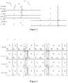
Fig.1 is a structural schematic diagram of a capacitive in-cell touch screen panel provided in the embodiments of present disclosure;Fig.2 is a structural schematic diagram of a TFT array substrate for the touch screen panel provided in the embodiments of present disclosure;Fig.3 is one of the structural schematic diagrams of a driving control unit of the touch screen panel provided in the embodiments of present disclosure;Fig.4 is the other one of the structural schematic diagrams of a driving control unit of the touch screen panel provided in the embodiments of present disclosure;Figs.5a-5c are structural schematic diagrams of color film substrate of the touch screen panel provided in the embodiments of present disclosure; andFig.6 is a schematic diagram of the connection relationship of the touch control inducting lines provided in the embodiments of present disclosure.- The capacitive in-cell touch screen panel and the display device provided by the embodiments of the present disclosure will be described below in detail in combination with the drawings.
- The film thickness and region size of the layers in the drawings do not reflect the real scale of the TFT array substrate or the color film substrate but are only for the purpose of illustrating the content of the present disclosure.
- As shown in
Fig.1 , a capacitive in-cell touch screen panel provided in an embodiment of the present disclosure comprises a color film substrate1, a TFT array substrate2 and aliquid crystal layer 3 between the color film substrate1and the TFT array substrate2, a plurality ofpixel units 4 being disposed in a matrix arrangement on the TFT array substrate2, and further comprises: - at least one touch
control driving electrode 5 on the TFT array substrate2, a top view of the TFT array substrate2 being shown inFig.2 from which it can be seen that apixel unit 4 is consisted of three sub-pixel units RGB (that is, apixel unit 4 on the TFT array substrate2 corresponds to three sub-pixel units RGB) on the color film substrate, the touchcontrol driving electrode 5 extends along the row direction of thepixel unit 4 and overlaps with multiple sets of gate lines in the TFT array substrate, each set of gate lines comprising at least two adjacent gate lines (Fig.2 takes a set of gate lines being consisted of two adjacent gate lines as an example, such as a set of gate line n and gate line n+1); each touchcontrol driving electrode 5 comprising touchcontrol driving sub-electrodes 51 disposed along the row direction which are positioned between theadjacent pixel units 4, respectively; driving control units 7 each positioned at the connection of each touchcontrol driving electrode 51 and each set of gate lines, thedriving control units 7 being used for delivering a display driving signal delivered by one gate line of the set of gate lines connected with thedriving control unit 7 to the touchcontrol driving sub-electrodes 51 as a touch control driving signal, and then outputting the touch control driving signal of the touchcontrol driving sub-electrodes 51; and- at least one touch control inducting electrode disposed 6 on the color film substrate1, the touch
control inducting electrode 6 extending along a column direction of thepixel units 4 as shown inFig.1 . - In the touch screen panel provided in the embodiment of the present disclosure, since the driving control units are able to load the display driving signal delivered by the gate lines to the touch control driving sub-electrodes and then release it, which is equivalent to loading a driving pulse on the touch control driving sub-electrodes, so that the multiple sets of gate lines overlapping the touch control driving electrodes input touch control driving signals to the touch control driving electrodes sequentially through the driving control units, thereby a plurality of driving pulses can be loaded on the touch control driving sub-electrodes, increasing the frequency of the touch control driving signals loaded on the touch control driving electrodes when the display driving signals of the gate lines are taken as the touch control driving signals.
- In particular, as shown in
Fig.3 , if each set of the gate lines includes two adjacent gate lines, for example, taking gate line n and gate line n+1 shown inFig.3 as one set, and so on there are four sets of gate lines connected with the touchcontrol driving sub-electrodes 51, and then thedriving control unit 7 comprises asignal input device 71 and asignal output device 72, wherein,
thesignal input device 71 is connected with the touchcontrol driving sub-electrodes 51 and the first gate line of the set of gate lines (e.g. gate line n, gate line m, gate line a or gate line b as shown inFig.3 ) so as to deliver the display driving signal delivered by the first gate line to the touchcontrol driving sub-electrodes 51 as the touch control driving signal; and
thesignal output device 72 is connected with the touchcontrol driving sub-electrodes 51 and two gate lines of the set of gate lines (e.g. gate lines n and n+1, gate lines m and m+1, gate lines a and a+1, or gate lines b and b+1 as shown inFig.3 ) so as to output the touch control driving signal of the touch control driving sub-electrodes to the first gate line of the set of gate lines, when the second gate line of the set of gate lines (e.g. gate line n+1, gate line m+1, gate line a+1, or gate line b+1 as shown inFig.3 ) is delivering the display driving signal. The first gate line is at a constant low level (Vgl) when the second gate line is opened. At the same time, the current of the touch control driving signal input to the first gate line will be conducted away, which will not cause a notable fluctuation on the low level (Vgl) of the first gate line, that is, the current will not make the TFT connected with the first gate line turn on such that the signal disturbance will not occur. - In implementations, however, the number of gate lines in each set is not limited to the two gate lines as illustrated above, and can be for example three gate lines wherein there is not any connection at the overlap of the last gate line and the touch control driving sub-electrode, and the last gate line can be connected with the touch control driving sub-electrode through the
driving control unit 7. For example, in addition to thesignal input device 71 andsignal output device 72, thedriving control unit 7 may include another signal output device which is connected with the touch control driving sub-electrode and the second and the last gate lines of the set of gate lines so as to output the touch control driving signal of the touch control driving sub-electrode to the second gate line of the set of gate lines when the last gate line of the set is delivering the display driving signal. It can be seen that the frequency of the touch control signal loaded on the touchcontrol driving sub-electrode 51 is lower in the implementation with three gate lines as one set than that in the implementation with two gate lines as one set. Therefore the implementation with two gate lines as one set is usually employed in order to increase the frequency of the touch control driving signal as much as possible. - In implementations, as shown in
Fig.4 , thesignal input device 71 andsignal output device 72 may be two TFT switches, that is, thesignal input device 71 may be a first TFT device and thesignal output device 72 may be a second TFT device; wherein,
a gate and a source of the first TFT device are connected with the first gate line of the set of gate lines (e.g. gate line n or gate line n+2 as shown inFig.4 ), and a drain thereof is connected with the touchcontrol driving sub-electrode 51; as such, when the display driving signal is loaded on the first gate line, the first TFT device is turned on such that the display driving signal of the first gate line is loaded to the touchcontrol driving sub-electrode 51 as the touch control driving signal, making the touchcontrol driving sub-electrode 51 at a high level;
a gate of the second TFT device is connected with the second gate line of the set of gate lines (e.g. gate line n+1 or gate line n+3 as shown inFig.4 ), a source thereof is connected with the touch control driving sub-electrode, and the drain thereof is connected with the first gate line of the set of gate lines; as such, after the display driving signal is loaded on the first gate line and when the display driving signal is loaded on the second gate line, the second TFT device is turned on such that the touch control driving signal loaded on the touchcontrol driving sub-electrode 51 by the first gate line is released on the first gate line, making the touchcontrol driving sub-electrode 51 at a low level. - In implementations, the touch control driving sub-electrode and the source and drain in the TFT array substrate can be disposed in the same layer. That is, the patterns of the source and drain of the TFT and the touch control driving sub-electrode are fabricated simultaneously in a patterning process, and thus no new patterning process will be added in the fabricating process for the TFT array substrate, and the cost for manufacturing the TFT array substrate as the touch screen panel will not be increased, either.
- In particular, since the touch control driving sub-electrode in each of the touch control driving electrodes is disposed at the gaps between the pixel units, the width of each of the touch control driving sub-electrode will not be larger than the gap between the adjacent columns of pixel units. In implementations, the width of each of the touch control driving sub-electrode may be set to be substantially the same as the width of the RGB sub-pixels.
- In general, the precision of the touch screen panel is usually in the order of millimeter, while the precision of the liquid crystal is usually in the order of micrometer. The precision of the touch screen panel relies on the length of the touch control driving sub-electrode, that is, the length of touch control driving sub-electrode can be selected in accordance with the required touch control precision. Consequently, the length of each of touch control driving sub-electrodes will span multiple columns of pixel units of the liquid crystal display, and is usually above 2mm. As such, each of the touch control driving sub-electrodes overlaps with multiple gate lines providing the display driving signal for the TFT in the TFT array substrate, and a parasitic capacitance is generated at the overlap thereof. The larger the area of the overlap is, the larger the parasitic capacitance is. The parasitic capacitance may incur the bad quality defects such as green pictures, line residual images and so on, which will be more obvious as the size of the panel increases.
- Accordingly, in the implementations, in order to reduce the area of the overlap of the touch control driving sub-electrodes and the gate lines, the parasitic capacitance is reduced. As shown in
Fig.4 , each of the touchcontrol driving sub-electrodes 51 may be a plurality of driving point electrodes which are electrically connected and are adjacent to each other in the column direction. The driving point electrodes are positioned between the adjacent column pixel units in each of the rows and are connected with each other through leads.Fig.4 illustrates an example of a touchcontrol driving sub-electrode 51 being consisted of four driving point electrodes. In this case, the area of the overlap of the leads and the gate lines is small and thus the generated parasitic capacitance can be reduced as much as possible. - In specific implementations, the touch control inducting electrode on the color film substrate can be positioned between the substrate and the colored resin of the colore film substrate or positioned on the side of the colored resin of the color film substrate facing the liquid crystal layer.
- In general, there are color filtering units on the color film substrate corresponding to the pixel units of the TFT array substrate, which are also consisted of three sub color filtering units R, G and B. Since the touch control inducting electrodes are wired along the column direction of the pixel units, in specific, the region of the projection of the touch control inducting electrodes on the TFT array substrate can be entirely covered between the adjacent columns of the pixel units or partially cover this gap; that is, the touch control inducting electrodes on the color film substrate exactly corresponds to the gap region between the adjacent columns of the pixel units on the TFT array substrate, or to a part of this gap region in spatial positions. As shown in
Fig.5a , the touchcontrol inducting electrodes 6 can be entirely disposed between thecolor filtering units 8 of the adjacent columns on the color film substrate, or in option, can be disposed between part of the adjacent columns of thecolor filtering units 8 as shown inFig.5b . For example, a touchcontrol inducting electrodes 6 is disposed at a gap of every other column of thecolor filtering units 8, details omitted here. In the practical manufacturing process, the distribution density of the touchcontrol inducting electrodes 6 can be set in accordance with the requirement of the touch control precision. - Furthermore, the shielding electrodes, which are fabricated on the side of the color film substrate backing against the liquid crystal layer in the prior art, can be fabricated on the side of the color film substrate facing the liquid crystal layer, which facilitates the thinning process performed on the coupled board after the color film substrate and the TFT array substrate are coupled, that is, the substrate exposed outside is etched with particular liquid. In specific, the shielding electrodes can be disposed between the substrate and the colored resin of the color film substrate, or disposed at the side of the colored resin facing the liquid crystal layer in the color film substrate. In implementations, the common electrode signal is input to the shielding electrode through the common electrode line electrically connected to the shielding electrode so as to shield the interference from the external signals. Preferably, manufacturing the shielding electrode between the substrate and the colored resin of the color film substrate is more advantageous for the shielding electrode to shield the interference from the external signals.
- Furthermore, the shielding electrodes which are fabricated entirely in a layer in the prior art is optimized into the strip-shaped shielding electrodes, and the projection area of one shielding electrode strip on the TFT array substrate entirely covers a column of pixel units. That is, as shown in
Figs.5a and5b , on the color film substrate, a shieldingelectrode strip 9 covers a column ofcolor filtering units 8 consisted of RGB. As such, when the projection area of each of the touch control inducting electrode strips on the TFT array substrate entirely or partially covers the gap between the adjacent columns of the pixel units, since the patterns of the shieldingelectrodes 9 and the touchcontrol inducting electrodes 6 are not overlapped with each other as shown inFig.5a andFig.5b , the shielding electrodes and the touch control inducting electrodes can also be disposed in the same layer. Of course, the shielding electrodes and the touch control inducting electrodes can be disposed in different layers of the color film substrate and the present disclosure is not limited thereto. - Furthermore, in addition to the disposition wherein the projection area of each of the touch control inducting electrode strips on the TFT array substrate entirely or partially covers the gap between the adjacent columns of the pixel units, the projection area of each of the touch control inducting electrode strips can also cover a column of pixel units. That is, as shown in
Fig.5c , a touchcontrol inducting electrode 6 covers a column of color filtering units in which case the common electrode signal can be loaded to the touchcontrol inducting electrode 6 at the same time, serving as shielding electrodes and omitting the shielding electrodes. - Accordingly, since the precision of the touch screen panel is usually in the order of millimeter and that of the liquid crystal display is usually in the order of micrometer, a plurality of adjacent touch control inducting electrodes can be used as a touch control inducting electrode strip. In implementations, M adjacent touch control inducting lines can be connected at either end through leads according to the required touch control pricision so as to be used as a touch control inducting electrode strip. An example in which three touch
control inducting strips 6 are connected at one end through the leads is shown inFig.6 . After the three touchcontrol inducting strips 6 are conducted to be one touch control inducting electrode strip, it is connected with the Touch FPC by using the sealant in the fanout area of the color film substrate, thereby reducing the wiring in the fanout area. - Base on the same inventive conception, there is also provided a display apparatus in an embodiment of present disclosure comprising the capacitive in-cell touch screen panel provided in the above embodiments. Please refer to the embodiments of the capacitive in-cell touch screen described above for those of the display apparatus and the repetition is omitted.
- In the capacitive in-cell touch screen panel and the display apparatus provided in the embodiments of present disclosure, at least one touch control inducting electrode is disposed on the color film substrate and at least one touch control driving electrode is disposed on the TFT array substrate. Each of the touch control driving electrodes overlaps with multiple sets of gate lines in the TFT array substrate, respectively, wherein a set of gate lines comprises at least two adjacent gate lines, each of the touch control driving electrodes comprises touch control driving sub-electrodes disposed along the row direction and a driving control unit is disposed at the connection of each of the touch control driving sub-electrodes and each set of gate lines. The driving control unit is configured for delivering a display driving signal delivered by a gate line of the set connected with the driving control unit to the touch control driving sub-electrodes as a touch control driving signal and then outputting the touch control driving signal of the touch control driving sub-electrodes. Since the driving control unit is able to release the display driving signal delivered by the gate line after it is loaded to the touch control driving sub-electrodes, which is equivalent to the situation where a driving pulse is loaded on the touch control driving sub-electrodes, the multiple sets of gate lines overlapping with the touch control driving electrodes input the touch control driving signal sequentially to the touch control driving electrodes through the driving control unit, and thus a plurality of driving pulses can be loaded on the touch control driving sub-electrodes, increasing the frequency of the touch control driving signal loaded on the touch control driving electrodes when the display driving signal of the gate lines is taken as the touch control driving signal.
- It is obvious that various changes and variations can be made to the present embodiments by those skilled in the art without departing from the scope of present disclosure. As such, it is intended such changes or variations are included in the present disclosure if they belongs to the scope of the present claims.
Claims (12)
- A capacitive in-cell touch screen panel, comprising: a color film substrate (1), a thin film transistor TFT array substrate (2) and a liquid crystal layer (3) between the color film substrate (1) and the TFT array substrate (2), a plurality of pixel units (4) being disposed in a matrix arrangement in the capacitive in-cell touch screen panel; at least one touch control driving electrode (5) disposed on the TFT array substrate (2) which extends along a row direction of the pixel units (4) and overlaps with multiple sets of gate lines (n,n+1,m,m+1,a,a+1,b,b+1) for providing display driving signal in the TFT array substrate (2), respectively, a set of gate lines including at least two adjacent gate lines (n,n+1), each of the touch control driving electrodes (5) comprising touch control driving sub-electrodes (51) disposed along the row direction;
a driving control unit (7) disposed at the connection of each of the touch control driving sub-electrodes (51) and each set of gate lines, the driving control unit (7) being configured for delivering a display driving signal delivered by a gate line of the set of gate lines connected with the driving control unit (7) to the touch control driving sub-electrodes (51) as a touch control driving signal and then outputting the touch control driving signal of the touch control driving sub-electrodes (51); and
at least one touch control inducting electrode (6) disposed on the color film substrate (1) which extends along a column direction of the pixel units (4). - The touch screen panel according to claim 1,characterized in that each set of the gate lines comprises two adjacent gate lines (n,n+1), and the driving control unit (7) comprises a signal input device (71) and a signal output device (72), wherein,
the signal input device (71) is configured for delivering a display driving signal delivered by a first gate line (n) to the touch control driving sub-electrodes (51) as a touch control driving signal; and
the signal output device (72) is configured for outputting the touch control driving signal of the touch control driving sub-electrodes to the first gate line of said set of gate lines when a second gate line (n+1) of said set of gate lines (n,n+1) delivers the display driving signal. - The touch screen panel according to claim 2,characterized in that the signal input device (71) is a first TFT device and the signal output device (72) is a second TFT device, wherein,
a gate and a source of the first TFT device are connected with the first gate line (n) of said set of gate lines (n,n+1) and a drain thereof is connected with the touch control driving sub-electrode (51);
a gate of the second TFT device is connected with the second gate line (n+1) of said set of gate lines (n,n+1), a source thereof is connected with the touch control driving sub-electrode, and a drain thereof is connected with the first gate line (n) of said set of gate lines. - The touch screen panel according to any one of claims 1-3,characterized in that the touch control driving sub-electrode (51) and the sources and the drains of the TFTs in the TFT array substrate are disposed in the same layer.
- The touch screen panel according to any one of claims 1-3,characterized in that each of the touch control driving sub-electrodes (51) comprises a plurality of driving point electrodes which are electrically connected and are adjacent to each other in the column direction, the driving point electrodes being positioned between the adjacent columns of pixel units in each of the rows.
- The touch screen panel according to claim 1,characterized in that the touch control inducting electrode (6) is positioned between the substrate of the color film substrate and the colored resin thereof, or positioned on a side of a colored resin of the color film substrate facing the liquid crystal layer.
- The touch screen panel according to claim 6,characterized in that a projection area of each of the touch control inducting electrodes (6) on the TFT array substrate covers a column of pixel units.
- The touch screen panel according to claim 6,characterized in that a projection area of each of the touch control inducting electrodes on the TFT array substrate entirely or partially covers a gap between the adjacent columns of the pixel units.
- The touch screen panel according to claim 8,characterized in that the color film substrate further comprises shielding electrodes (9) which are positioned between a substrate of the color film substrate and a colored resin thereof, or positioned on a side of the colored resin of the color film substrate facing the liquid crystal layer,
wherein a projection area of one shielding electrode on the TFT array substrate entirely covers a column of pixel units. - The touch screen panel according to claim 9,characterized in that the shielding electrodes (9) and the touch control driving electrodes (6) are disposed in the same layer.
- The touch screen panel according to any one of claims 6-10,characterized in that a plurality of adjacent touch control inducting lines are connected at either end through leads.
- A display apparatuscharacterized in comprising the capacitive in-cell touch screen panel according to any one of claims 1-11.
Applications Claiming Priority (1)
| Application Number | Priority Date | Filing Date | Title |
|---|---|---|---|
| CN201210321910.0ACN102866815B (en) | 2012-09-03 | 2012-09-03 | Capacitance type embedded touch screen and display device |
Publications (3)
| Publication Number | Publication Date |
|---|---|
| EP2703969A2 EP2703969A2 (en) | 2014-03-05 |
| EP2703969A3 EP2703969A3 (en) | 2016-08-03 |
| EP2703969B1true EP2703969B1 (en) | 2018-04-04 |
Family
ID=47445710
Family Applications (1)
| Application Number | Title | Priority Date | Filing Date |
|---|---|---|---|
| EP13182825.3ANot-in-forceEP2703969B1 (en) | 2012-09-03 | 2013-09-03 | Capacitive in-cell touch screen panel and display device |
Country Status (3)
| Country | Link |
|---|---|
| US (1) | US9292139B2 (en) |
| EP (1) | EP2703969B1 (en) |
| CN (1) | CN102866815B (en) |
Families Citing this family (42)
| Publication number | Priority date | Publication date | Assignee | Title |
|---|---|---|---|---|
| KR101602199B1 (en)* | 2012-12-11 | 2016-03-10 | 엘지디스플레이 주식회사 | Display device with integrated touch screen and method for driving the same |
| CN104035699A (en)* | 2013-03-05 | 2014-09-10 | 中兴通讯股份有限公司 | Capacitive touch screen terminal and input method thereof |
| CN103257769B (en)* | 2013-03-25 | 2016-01-27 | 合肥京东方光电科技有限公司 | A kind of electric capacity In-cell touch panel and display device |
| CN103226412A (en)* | 2013-04-10 | 2013-07-31 | 北京京东方光电科技有限公司 | In-cell touch panel and display device |
| CN103294317B (en) | 2013-05-31 | 2016-03-30 | 京东方科技集团股份有限公司 | A kind of array base palte, contact panel and display device |
| WO2015131308A1 (en)* | 2014-03-03 | 2015-09-11 | Nokia Technologies Oy | Capacitive touch sensor circuit, method of forming circuit, and touch screen and mobile device comprising the same |
| CN103984456A (en)* | 2014-04-28 | 2014-08-13 | 惠州市德帮实业有限公司 | Capacitive touch screen-based gesture sensing device and capacitive touch screen-based gesture recognition method |
| CN103995633B (en) | 2014-05-06 | 2017-03-22 | 京东方科技集团股份有限公司 | Touch display device and drive method thereof |
| CN104020906B (en)* | 2014-05-30 | 2016-09-07 | 京东方科技集团股份有限公司 | A kind of In-cell touch panel and display device |
| US9444015B2 (en) | 2014-06-18 | 2016-09-13 | X-Celeprint Limited | Micro assembled LED displays and lighting elements |
| US9799261B2 (en) | 2014-09-25 | 2017-10-24 | X-Celeprint Limited | Self-compensating circuit for faulty display pixels |
| US9991163B2 (en) | 2014-09-25 | 2018-06-05 | X-Celeprint Limited | Small-aperture-ratio display with electrical component |
| US9799719B2 (en) | 2014-09-25 | 2017-10-24 | X-Celeprint Limited | Active-matrix touchscreen |
| CN104298404B (en) | 2014-10-28 | 2017-05-31 | 上海天马微电子有限公司 | Array substrate and manufacturing method thereof, display device and driving method thereof |
| CN104571695A (en)* | 2014-12-24 | 2015-04-29 | 深圳莱宝高科技股份有限公司 | Touch display device |
| CN104699353B (en)* | 2015-04-01 | 2018-02-06 | 上海天马微电子有限公司 | Array substrate, driving method, display panel and display device |
| US9871345B2 (en) | 2015-06-09 | 2018-01-16 | X-Celeprint Limited | Crystalline color-conversion device |
| US10133426B2 (en)* | 2015-06-18 | 2018-11-20 | X-Celeprint Limited | Display with micro-LED front light |
| US11061276B2 (en) | 2015-06-18 | 2021-07-13 | X Display Company Technology Limited | Laser array display |
| CN104898892B (en) | 2015-07-09 | 2017-11-17 | 京东方科技集团股份有限公司 | A kind of touch-control display panel and preparation method thereof, touch control display apparatus |
| US10255834B2 (en) | 2015-07-23 | 2019-04-09 | X-Celeprint Limited | Parallel redundant chiplet system for controlling display pixels |
| WO2017060487A2 (en)* | 2015-10-08 | 2017-04-13 | X-Celeprint Limited | Display with integrated electrodes |
| US10380930B2 (en) | 2015-08-24 | 2019-08-13 | X-Celeprint Limited | Heterogeneous light emitter display system |
| KR102381130B1 (en) | 2015-08-31 | 2022-03-30 | 엘지디스플레이 주식회사 | And Touch Display Device And Method Of Driving The Same, And Display Panel |
| CN105117088B (en) | 2015-09-16 | 2018-03-23 | 京东方科技集团股份有限公司 | A kind of touch-control display panel and preparation method thereof, driving method |
| CN105159516B (en)* | 2015-09-18 | 2018-01-12 | 深圳市华星光电技术有限公司 | Touch-control display panel and touch control display apparatus |
| US10230048B2 (en) | 2015-09-29 | 2019-03-12 | X-Celeprint Limited | OLEDs for micro transfer printing |
| US10066819B2 (en) | 2015-12-09 | 2018-09-04 | X-Celeprint Limited | Micro-light-emitting diode backlight system |
| CN105629597B (en)* | 2016-01-14 | 2019-06-21 | 京东方科技集团股份有限公司 | Array substrate and display driving method, manufacturing method and display device thereof |
| US10193025B2 (en) | 2016-02-29 | 2019-01-29 | X-Celeprint Limited | Inorganic LED pixel structure |
| US10153257B2 (en) | 2016-03-03 | 2018-12-11 | X-Celeprint Limited | Micro-printed display |
| US10153256B2 (en) | 2016-03-03 | 2018-12-11 | X-Celeprint Limited | Micro-transfer printable electronic component |
| TWI740908B (en)* | 2016-03-11 | 2021-10-01 | 南韓商三星顯示器有限公司 | Display apparatus |
| US10199546B2 (en) | 2016-04-05 | 2019-02-05 | X-Celeprint Limited | Color-filter device |
| US10008483B2 (en) | 2016-04-05 | 2018-06-26 | X-Celeprint Limited | Micro-transfer printed LED and color filter structure |
| US9997501B2 (en) | 2016-06-01 | 2018-06-12 | X-Celeprint Limited | Micro-transfer-printed light-emitting diode device |
| US11137641B2 (en) | 2016-06-10 | 2021-10-05 | X Display Company Technology Limited | LED structure with polarized light emission |
| US9980341B2 (en) | 2016-09-22 | 2018-05-22 | X-Celeprint Limited | Multi-LED components |
| US10782002B2 (en) | 2016-10-28 | 2020-09-22 | X Display Company Technology Limited | LED optical components |
| US10347168B2 (en) | 2016-11-10 | 2019-07-09 | X-Celeprint Limited | Spatially dithered high-resolution |
| CN110376814B (en)* | 2019-07-29 | 2022-08-26 | 昆山龙腾光电股份有限公司 | Array substrate and embedded touch display panel |
| CN119065523A (en)* | 2023-06-02 | 2024-12-03 | 北京京东方显示技术有限公司 | Display panel and display device |
Family Cites Families (10)
| Publication number | Priority date | Publication date | Assignee | Title |
|---|---|---|---|---|
| US20090079707A1 (en)* | 2007-09-24 | 2009-03-26 | Motorola, Inc. | Integrated capacitive sensing devices and methods |
| JP4816668B2 (en)* | 2008-03-28 | 2011-11-16 | ソニー株式会社 | Display device with touch sensor |
| CN102436107B (en)* | 2009-03-26 | 2014-06-18 | 友达光电股份有限公司 | Liquid crystal display device and control method thereof |
| CN102289093B (en)* | 2010-06-17 | 2013-10-09 | 北京京东方光电科技有限公司 | Base board, manufacturing method thereof, LCD (Liquid Crystal Display) and touch addressing method |
| KR101761580B1 (en)* | 2010-09-08 | 2017-07-27 | 엘지디스플레이 주식회사 | Display device having touch sensor |
| TWI439050B (en)* | 2010-10-27 | 2014-05-21 | Au Optronics Corp | Shift register and touch device |
| KR101503103B1 (en)* | 2011-03-25 | 2015-03-17 | 엘지디스플레이 주식회사 | Touch sensor integrated type display and driving method therefrom |
| CN102830879B (en)* | 2012-08-17 | 2015-09-09 | 北京京东方光电科技有限公司 | A kind of In-cell touch panel |
| CN202736016U (en)* | 2012-09-03 | 2013-02-13 | 北京京东方光电科技有限公司 | Capacitive embedded touch screen and display device |
| KR102004924B1 (en)* | 2012-12-09 | 2019-10-01 | 엘지디스플레이 주식회사 | Display Device and Method for touch sencing of the same |
- 2012
- 2012-09-03CNCN201210321910.0Apatent/CN102866815B/ennot_activeExpired - Fee Related
- 2013
- 2013-08-12USUS13/964,557patent/US9292139B2/ennot_activeExpired - Fee Related
- 2013-09-03EPEP13182825.3Apatent/EP2703969B1/ennot_activeNot-in-force
Non-Patent Citations (1)
| Title |
|---|
| None* |
Also Published As
| Publication number | Publication date |
|---|---|
| EP2703969A3 (en) | 2016-08-03 |
| CN102866815B (en) | 2015-07-01 |
| US20140062944A1 (en) | 2014-03-06 |
| EP2703969A2 (en) | 2014-03-05 |
| CN102866815A (en) | 2013-01-09 |
| US9292139B2 (en) | 2016-03-22 |
Similar Documents
| Publication | Publication Date | Title |
|---|---|---|
| EP2703969B1 (en) | Capacitive in-cell touch screen panel and display device | |
| CN102841716B (en) | A kind of capacitance type in-cell touch panel and display device | |
| JP6130501B2 (en) | Capacitive in-cell touch screen panel, touch positioning method thereof, and display device | |
| US10042490B2 (en) | Array substrate, display device and driving method | |
| EP2889674B1 (en) | Built-in capacitive touch screen crystal display module and driving method thereof | |
| US9170691B2 (en) | Capacitive in cell touch panel and driving method thereof, display device | |
| US9772723B2 (en) | Capacitive in-cell touch panel and display device | |
| US20160011688A1 (en) | In-cell touch screen and display apparatus | |
| CN102968231B (en) | A kind of capacitance type in-cell touch panel, its driving method and display device | |
| US20160026291A1 (en) | In-cell touch panel and display device | |
| EP2720124A2 (en) | A capacitive in cell touch panel and display device | |
| US20140125626A1 (en) | Capacitive in-cell touch screen, driving method for the same, and display apparatus | |
| US20160283009A1 (en) | In-cell touch panel and display device | |
| US10338710B2 (en) | In-cell touch panel and display device | |
| US20180275809A1 (en) | In-cell touch screen and display device | |
| CN104570446B (en) | A kind of touch-control display panel and its control method | |
| WO2010029662A1 (en) | Display device | |
| CN103019492A (en) | Embedded capacitive touch control display panel, display equipment, control device and control method | |
| EP3236342B1 (en) | Touch display panel and driving method therefor, and touch display device | |
| TWI588577B (en) | Subpixel structure of display device and touch screen-integrated display device having the same | |
| US20170277329A1 (en) | Touch Screen and Driving Method Thereof, and Display Apparatus | |
| CN202711227U (en) | Capacitive in-cell touch panel and display device | |
| CN202976052U (en) | Embedded capacitive touch display panel, display equipment and control device | |
| JP2011170784A (en) | Display device with touch panel | |
| CN202736016U (en) | Capacitive embedded touch screen and display device |
Legal Events
| Date | Code | Title | Description |
|---|---|---|---|
| AK | Designated contracting states | Kind code of ref document:A2 Designated state(s):AL AT BE BG CH CY CZ DE DK EE ES FI FR GB GR HR HU IE IS IT LI LT LU LV MC MK MT NL NO PL PT RO RS SE SI SK SM TR | |
| AX | Request for extension of the european patent | Extension state:BA ME | |
| PUAI | Public reference made under article 153(3) epc to a published international application that has entered the european phase | Free format text:ORIGINAL CODE: 0009012 | |
| PUAL | Search report despatched | Free format text:ORIGINAL CODE: 0009013 | |
| AK | Designated contracting states | Kind code of ref document:A3 Designated state(s):AL AT BE BG CH CY CZ DE DK EE ES FI FR GB GR HR HU IE IS IT LI LT LU LV MC MK MT NL NO PL PT RO RS SE SI SK SM TR | |
| AX | Request for extension of the european patent | Extension state:BA ME | |
| RIC1 | Information provided on ipc code assigned before grant | Ipc:G02F 1/1333 20060101ALI20160628BHEP Ipc:G06F 3/044 20060101AFI20160628BHEP Ipc:G06F 3/041 20060101ALI20160628BHEP | |
| 17P | Request for examination filed | Effective date:20170202 | |
| RBV | Designated contracting states (corrected) | Designated state(s):AL AT BE BG CH CY CZ DE DK EE ES FI FR GB GR HR HU IE IS IT LI LT LU LV MC MK MT NL NO PL PT RO RS SE SI SK SM TR | |
| GRAP | Despatch of communication of intention to grant a patent | Free format text:ORIGINAL CODE: EPIDOSNIGR1 | |
| INTG | Intention to grant announced | Effective date:20171011 | |
| GRAS | Grant fee paid | Free format text:ORIGINAL CODE: EPIDOSNIGR3 | |
| GRAA | (expected) grant | Free format text:ORIGINAL CODE: 0009210 | |
| AK | Designated contracting states | Kind code of ref document:B1 Designated state(s):AL AT BE BG CH CY CZ DE DK EE ES FI FR GB GR HR HU IE IS IT LI LT LU LV MC MK MT NL NO PL PT RO RS SE SI SK SM TR | |
| REG | Reference to a national code | Ref country code:GB Ref legal event code:FG4D | |
| REG | Reference to a national code | Ref country code:CH Ref legal event code:EP | |
| REG | Reference to a national code | Ref country code:AT Ref legal event code:REF Ref document number:986262 Country of ref document:AT Kind code of ref document:T Effective date:20180415 | |
| REG | Reference to a national code | Ref country code:DE Ref legal event code:R096 Ref document number:602013035315 Country of ref document:DE | |
| REG | Reference to a national code | Ref country code:IE Ref legal event code:FG4D | |
| REG | Reference to a national code | Ref country code:NL Ref legal event code:FP | |
| REG | Reference to a national code | Ref country code:FR Ref legal event code:PLFP Year of fee payment:6 | |
| REG | Reference to a national code | Ref country code:LT Ref legal event code:MG4D | |
| PG25 | Lapsed in a contracting state [announced via postgrant information from national office to epo] | Ref country code:PL Free format text:LAPSE BECAUSE OF FAILURE TO SUBMIT A TRANSLATION OF THE DESCRIPTION OR TO PAY THE FEE WITHIN THE PRESCRIBED TIME-LIMIT Effective date:20180404 Ref country code:SE Free format text:LAPSE BECAUSE OF FAILURE TO SUBMIT A TRANSLATION OF THE DESCRIPTION OR TO PAY THE FEE WITHIN THE PRESCRIBED TIME-LIMIT Effective date:20180404 Ref country code:ES Free format text:LAPSE BECAUSE OF FAILURE TO SUBMIT A TRANSLATION OF THE DESCRIPTION OR TO PAY THE FEE WITHIN THE PRESCRIBED TIME-LIMIT Effective date:20180404 Ref country code:AL Free format text:LAPSE BECAUSE OF FAILURE TO SUBMIT A TRANSLATION OF THE DESCRIPTION OR TO PAY THE FEE WITHIN THE PRESCRIBED TIME-LIMIT Effective date:20180404 Ref country code:LT Free format text:LAPSE BECAUSE OF FAILURE TO SUBMIT A TRANSLATION OF THE DESCRIPTION OR TO PAY THE FEE WITHIN THE PRESCRIBED TIME-LIMIT Effective date:20180404 Ref country code:FI Free format text:LAPSE BECAUSE OF FAILURE TO SUBMIT A TRANSLATION OF THE DESCRIPTION OR TO PAY THE FEE WITHIN THE PRESCRIBED TIME-LIMIT Effective date:20180404 Ref country code:BG Free format text:LAPSE BECAUSE OF FAILURE TO SUBMIT A TRANSLATION OF THE DESCRIPTION OR TO PAY THE FEE WITHIN THE PRESCRIBED TIME-LIMIT Effective date:20180704 Ref country code:NO Free format text:LAPSE BECAUSE OF FAILURE TO SUBMIT A TRANSLATION OF THE DESCRIPTION OR TO PAY THE FEE WITHIN THE PRESCRIBED TIME-LIMIT Effective date:20180704 | |
| PG25 | Lapsed in a contracting state [announced via postgrant information from national office to epo] | Ref country code:GR Free format text:LAPSE BECAUSE OF FAILURE TO SUBMIT A TRANSLATION OF THE DESCRIPTION OR TO PAY THE FEE WITHIN THE PRESCRIBED TIME-LIMIT Effective date:20180705 Ref country code:LV Free format text:LAPSE BECAUSE OF FAILURE TO SUBMIT A TRANSLATION OF THE DESCRIPTION OR TO PAY THE FEE WITHIN THE PRESCRIBED TIME-LIMIT Effective date:20180404 Ref country code:HR Free format text:LAPSE BECAUSE OF FAILURE TO SUBMIT A TRANSLATION OF THE DESCRIPTION OR TO PAY THE FEE WITHIN THE PRESCRIBED TIME-LIMIT Effective date:20180404 Ref country code:RS Free format text:LAPSE BECAUSE OF FAILURE TO SUBMIT A TRANSLATION OF THE DESCRIPTION OR TO PAY THE FEE WITHIN THE PRESCRIBED TIME-LIMIT Effective date:20180404 | |
| REG | Reference to a national code | Ref country code:AT Ref legal event code:MK05 Ref document number:986262 Country of ref document:AT Kind code of ref document:T Effective date:20180404 | |
| PG25 | Lapsed in a contracting state [announced via postgrant information from national office to epo] | Ref country code:PT Free format text:LAPSE BECAUSE OF FAILURE TO SUBMIT A TRANSLATION OF THE DESCRIPTION OR TO PAY THE FEE WITHIN THE PRESCRIBED TIME-LIMIT Effective date:20180806 | |
| REG | Reference to a national code | Ref country code:DE Ref legal event code:R097 Ref document number:602013035315 Country of ref document:DE | |
| PG25 | Lapsed in a contracting state [announced via postgrant information from national office to epo] | Ref country code:DK Free format text:LAPSE BECAUSE OF FAILURE TO SUBMIT A TRANSLATION OF THE DESCRIPTION OR TO PAY THE FEE WITHIN THE PRESCRIBED TIME-LIMIT Effective date:20180404 Ref country code:SK Free format text:LAPSE BECAUSE OF FAILURE TO SUBMIT A TRANSLATION OF THE DESCRIPTION OR TO PAY THE FEE WITHIN THE PRESCRIBED TIME-LIMIT Effective date:20180404 Ref country code:RO Free format text:LAPSE BECAUSE OF FAILURE TO SUBMIT A TRANSLATION OF THE DESCRIPTION OR TO PAY THE FEE WITHIN THE PRESCRIBED TIME-LIMIT Effective date:20180404 Ref country code:CZ Free format text:LAPSE BECAUSE OF FAILURE TO SUBMIT A TRANSLATION OF THE DESCRIPTION OR TO PAY THE FEE WITHIN THE PRESCRIBED TIME-LIMIT Effective date:20180404 Ref country code:EE Free format text:LAPSE BECAUSE OF FAILURE TO SUBMIT A TRANSLATION OF THE DESCRIPTION OR TO PAY THE FEE WITHIN THE PRESCRIBED TIME-LIMIT Effective date:20180404 Ref country code:AT Free format text:LAPSE BECAUSE OF FAILURE TO SUBMIT A TRANSLATION OF THE DESCRIPTION OR TO PAY THE FEE WITHIN THE PRESCRIBED TIME-LIMIT Effective date:20180404 | |
| PLBE | No opposition filed within time limit | Free format text:ORIGINAL CODE: 0009261 | |
| STAA | Information on the status of an ep patent application or granted ep patent | Free format text:STATUS: NO OPPOSITION FILED WITHIN TIME LIMIT | |
| PG25 | Lapsed in a contracting state [announced via postgrant information from national office to epo] | Ref country code:IT Free format text:LAPSE BECAUSE OF FAILURE TO SUBMIT A TRANSLATION OF THE DESCRIPTION OR TO PAY THE FEE WITHIN THE PRESCRIBED TIME-LIMIT Effective date:20180404 Ref country code:SM Free format text:LAPSE BECAUSE OF FAILURE TO SUBMIT A TRANSLATION OF THE DESCRIPTION OR TO PAY THE FEE WITHIN THE PRESCRIBED TIME-LIMIT Effective date:20180404 | |
| 26N | No opposition filed | Effective date:20190107 | |
| PG25 | Lapsed in a contracting state [announced via postgrant information from national office to epo] | Ref country code:MC Free format text:LAPSE BECAUSE OF FAILURE TO SUBMIT A TRANSLATION OF THE DESCRIPTION OR TO PAY THE FEE WITHIN THE PRESCRIBED TIME-LIMIT Effective date:20180404 | |
| REG | Reference to a national code | Ref country code:CH Ref legal event code:PL | |
| PG25 | Lapsed in a contracting state [announced via postgrant information from national office to epo] | Ref country code:SI Free format text:LAPSE BECAUSE OF FAILURE TO SUBMIT A TRANSLATION OF THE DESCRIPTION OR TO PAY THE FEE WITHIN THE PRESCRIBED TIME-LIMIT Effective date:20180404 | |
| REG | Reference to a national code | Ref country code:BE Ref legal event code:MM Effective date:20180930 | |
| REG | Reference to a national code | Ref country code:IE Ref legal event code:MM4A | |
| PG25 | Lapsed in a contracting state [announced via postgrant information from national office to epo] | Ref country code:LU Free format text:LAPSE BECAUSE OF NON-PAYMENT OF DUE FEES Effective date:20180903 | |
| PG25 | Lapsed in a contracting state [announced via postgrant information from national office to epo] | Ref country code:IE Free format text:LAPSE BECAUSE OF NON-PAYMENT OF DUE FEES Effective date:20180903 | |
| PG25 | Lapsed in a contracting state [announced via postgrant information from national office to epo] | Ref country code:CH Free format text:LAPSE BECAUSE OF NON-PAYMENT OF DUE FEES Effective date:20180930 Ref country code:LI Free format text:LAPSE BECAUSE OF NON-PAYMENT OF DUE FEES Effective date:20180930 Ref country code:BE Free format text:LAPSE BECAUSE OF NON-PAYMENT OF DUE FEES Effective date:20180930 | |
| PG25 | Lapsed in a contracting state [announced via postgrant information from national office to epo] | Ref country code:MT Free format text:LAPSE BECAUSE OF NON-PAYMENT OF DUE FEES Effective date:20180903 | |
| PG25 | Lapsed in a contracting state [announced via postgrant information from national office to epo] | Ref country code:TR Free format text:LAPSE BECAUSE OF FAILURE TO SUBMIT A TRANSLATION OF THE DESCRIPTION OR TO PAY THE FEE WITHIN THE PRESCRIBED TIME-LIMIT Effective date:20180404 | |
| PG25 | Lapsed in a contracting state [announced via postgrant information from national office to epo] | Ref country code:HU Free format text:LAPSE BECAUSE OF FAILURE TO SUBMIT A TRANSLATION OF THE DESCRIPTION OR TO PAY THE FEE WITHIN THE PRESCRIBED TIME-LIMIT; INVALID AB INITIO Effective date:20130903 | |
| PG25 | Lapsed in a contracting state [announced via postgrant information from national office to epo] | Ref country code:CY Free format text:LAPSE BECAUSE OF FAILURE TO SUBMIT A TRANSLATION OF THE DESCRIPTION OR TO PAY THE FEE WITHIN THE PRESCRIBED TIME-LIMIT Effective date:20180404 Ref country code:MK Free format text:LAPSE BECAUSE OF NON-PAYMENT OF DUE FEES Effective date:20180404 | |
| PG25 | Lapsed in a contracting state [announced via postgrant information from national office to epo] | Ref country code:IS Free format text:LAPSE BECAUSE OF FAILURE TO SUBMIT A TRANSLATION OF THE DESCRIPTION OR TO PAY THE FEE WITHIN THE PRESCRIBED TIME-LIMIT Effective date:20180804 | |
| PGFP | Annual fee paid to national office [announced via postgrant information from national office to epo] | Ref country code:NL Payment date:20220922 Year of fee payment:10 Ref country code:GB Payment date:20220714 Year of fee payment:10 Ref country code:DE Payment date:20220920 Year of fee payment:10 | |
| PGFP | Annual fee paid to national office [announced via postgrant information from national office to epo] | Ref country code:FR Payment date:20220709 Year of fee payment:10 | |
| REG | Reference to a national code | Ref country code:DE Ref legal event code:R119 Ref document number:602013035315 Country of ref document:DE | |
| REG | Reference to a national code | Ref country code:NL Ref legal event code:MM Effective date:20231001 | |
| GBPC | Gb: european patent ceased through non-payment of renewal fee | Effective date:20230903 | |
| PG25 | Lapsed in a contracting state [announced via postgrant information from national office to epo] | Ref country code:NL Free format text:LAPSE BECAUSE OF NON-PAYMENT OF DUE FEES Effective date:20231001 | |
| PG25 | Lapsed in a contracting state [announced via postgrant information from national office to epo] | Ref country code:NL Free format text:LAPSE BECAUSE OF NON-PAYMENT OF DUE FEES Effective date:20231001 | |
| PG25 | Lapsed in a contracting state [announced via postgrant information from national office to epo] | Ref country code:GB Free format text:LAPSE BECAUSE OF NON-PAYMENT OF DUE FEES Effective date:20230903 | |
| PG25 | Lapsed in a contracting state [announced via postgrant information from national office to epo] | Ref country code:GB Free format text:LAPSE BECAUSE OF NON-PAYMENT OF DUE FEES Effective date:20230903 Ref country code:FR Free format text:LAPSE BECAUSE OF NON-PAYMENT OF DUE FEES Effective date:20230930 Ref country code:DE Free format text:LAPSE BECAUSE OF NON-PAYMENT OF DUE FEES Effective date:20240403 |